US11652288B2 - Antenna - Google Patents
Antenna Download PDFInfo
- Publication number
- US11652288B2 US11652288B2 US17/233,897 US202117233897A US11652288B2 US 11652288 B2 US11652288 B2 US 11652288B2 US 202117233897 A US202117233897 A US 202117233897A US 11652288 B2 US11652288 B2 US 11652288B2
- Authority
- US
- United States
- Prior art keywords
- metal ring
- antenna
- radiating elements
- antenna according
- ring
- Prior art date
- Legal status (The legal status is an assumption and is not a legal conclusion. Google has not performed a legal analysis and makes no representation as to the accuracy of the status listed.)
- Active, expires
Links
Images


Classifications
-
- H—ELECTRICITY
- H01—ELECTRIC ELEMENTS
- H01Q—ANTENNAS, i.e. RADIO AERIALS
- H01Q1/00—Details of, or arrangements associated with, antennas
- H01Q1/36—Structural form of radiating elements, e.g. cone, spiral, umbrella; Particular materials used therewith
-
- H—ELECTRICITY
- H01—ELECTRIC ELEMENTS
- H01Q—ANTENNAS, i.e. RADIO AERIALS
- H01Q1/00—Details of, or arrangements associated with, antennas
- H01Q1/50—Structural association of antennas with earthing switches, lead-in devices or lightning protectors
-
- H—ELECTRICITY
- H01—ELECTRIC ELEMENTS
- H01Q—ANTENNAS, i.e. RADIO AERIALS
- H01Q1/00—Details of, or arrangements associated with, antennas
- H01Q1/52—Means for reducing coupling between antennas; Means for reducing coupling between an antenna and another structure
-
- H—ELECTRICITY
- H01—ELECTRIC ELEMENTS
- H01Q—ANTENNAS, i.e. RADIO AERIALS
- H01Q1/00—Details of, or arrangements associated with, antennas
- H01Q1/52—Means for reducing coupling between antennas; Means for reducing coupling between an antenna and another structure
- H01Q1/521—Means for reducing coupling between antennas; Means for reducing coupling between an antenna and another structure reducing the coupling between adjacent antennas
-
- H—ELECTRICITY
- H01—ELECTRIC ELEMENTS
- H01Q—ANTENNAS, i.e. RADIO AERIALS
- H01Q19/00—Combinations of primary active antenna elements and units with secondary devices, e.g. with quasi-optical devices, for giving the antenna a desired directional characteristic
- H01Q19/10—Combinations of primary active antenna elements and units with secondary devices, e.g. with quasi-optical devices, for giving the antenna a desired directional characteristic using reflecting surfaces
-
- H—ELECTRICITY
- H01—ELECTRIC ELEMENTS
- H01Q—ANTENNAS, i.e. RADIO AERIALS
- H01Q21/00—Antenna arrays or systems
- H01Q21/06—Arrays of individually energised antenna units similarly polarised and spaced apart
-
- H—ELECTRICITY
- H01—ELECTRIC ELEMENTS
- H01Q—ANTENNAS, i.e. RADIO AERIALS
- H01Q21/00—Antenna arrays or systems
- H01Q21/24—Combinations of antenna units polarised in different directions for transmitting or receiving circularly and elliptically polarised waves or waves linearly polarised in any direction
- H01Q21/26—Turnstile or like antennas comprising arrangements of three or more elongated elements disposed radially and symmetrically in a horizontal plane about a common centre
-
- H—ELECTRICITY
- H01—ELECTRIC ELEMENTS
- H01Q—ANTENNAS, i.e. RADIO AERIALS
- H01Q5/00—Arrangements for simultaneous operation of antennas on two or more different wavebands, e.g. dual-band or multi-band arrangements
- H01Q5/20—Arrangements for simultaneous operation of antennas on two or more different wavebands, e.g. dual-band or multi-band arrangements characterised by the operating wavebands
-
- H—ELECTRICITY
- H01—ELECTRIC ELEMENTS
- H01Q—ANTENNAS, i.e. RADIO AERIALS
- H01Q1/00—Details of, or arrangements associated with, antennas
- H01Q1/12—Supports; Mounting means
- H01Q1/22—Supports; Mounting means by structural association with other equipment or articles
- H01Q1/24—Supports; Mounting means by structural association with other equipment or articles with receiving set
- H01Q1/241—Supports; Mounting means by structural association with other equipment or articles with receiving set used in mobile communications, e.g. GSM
- H01Q1/246—Supports; Mounting means by structural association with other equipment or articles with receiving set used in mobile communications, e.g. GSM specially adapted for base stations
-
- H—ELECTRICITY
- H01—ELECTRIC ELEMENTS
- H01Q—ANTENNAS, i.e. RADIO AERIALS
- H01Q1/00—Details of, or arrangements associated with, antennas
- H01Q1/42—Housings not intimately mechanically associated with radiating elements, e.g. radome
Definitions
- the present invention relates to a communication system, and more particularly, to an antenna suitable for use in a communication system.
- a geographic area is divided into a series of regions that are referred to as “cells” which are served by respective base stations.
- the base station may include one or more base station antennas that are configured to provide two-way radio frequency (“RF”) communications with mobile subscribers that are within the cell served by the base station.
- RF radio frequency
- each base station is divided into “sectors.” In perhaps the most common configuration, a hexagonally shaped cell is divided into three 120° sectors, and each sector is served by one or more base station antennas that have an azimuth Half Power Beam width (HPBW) of approximately 65°.
- HPBW azimuth Half Power Beam width
- the base station antennas are mounted on a tower, with the radiation patterns (also referred to herein as “antenna beams”) that are generated by the base station antennas directed outwardly.
- Base station antennas are often implemented as linear or planar phased arrays of radiating elements.
- Parasitic elements are typically used in the base station antennas to tune the radiation pattern of the arrays of radiating elements to thereby improve the shape of the antenna beams that are formed by the arrays.
- a proper arrangement of the parasitic elements may enhance radiation in a desired direction and attenuate radiation in undesired directions.
- the spacings between adjacent arrays are typically decreased, which results in increased coupling interference between the arrays. The increased coupling interference degrades the isolation performance of the radiating elements, which may negatively affect the performance the antenna.
- parasitic elements may be provided between adjacent radiating elements to improve the degree of isolation therebetween to thereby improve the radiation patterns of the base station antenna.
- antennas comprising a reflector, first and second arrays of first radiating elements mounted on the reflector, and a parasitic element that includes a metal ring.
- the metal ring of the parasitic element is arranged between a first radiating element of the first array and a first radiating element of the second array.
- the antennas according to the embodiments of the present invention may effectively improve the isolation between the first and second arrays, thereby improving the radiation patterns generated by the first and second arrays.
- arrays of first radiating elements are configured to generate first antenna beams in a first frequency band that includes at least a portion of a 1695-2690 MHz frequency band or a portion of a 3.1-4.2 GHz frequency band.
- a perimeter of the metal ring is between 80% and 120% of a reference wavelength, where the reference wavelength is equal to the wavelength corresponding to a reference frequency point in the first frequency band.
- the perimeter of the metal ring is an outer perimeter, an inner perimeter or an equivalent perimeter of the metal ring.
- the reference frequency point is a frequency point of an array of first radiating elements within the first frequency band with the worst degree of isolation, or the reference frequency point is set to be an average value of a plurality of frequency points of an array of first radiating elements within the first frequency band with worst degrees of isolation.
- the antenna array further comprises an array of second radiating elements, where the array of second radiating elements is configured to generate a second antenna beam in a second frequency band that includes at least a portion of the 694-960 MHz frequency band.
- the metal ring has an outer perimeter with at least 60%, or at least 80%, of the interior of the outer perimeter is free of metal.
- the metal ring is configured as a circular ring, a polygonal ring or an elliptical ring.
- the metal ring is configured as a closed ring.
- the metal ring is configured as an open ring with at least one slot.
- the metal ring is configured as a trace printed on a PCB board.
- the metal ring is constructed based on a magnetic dipole model
- the first radiating element is constructed based on an electric dipole model, such that the metal ring and the first radiating element have complementary characteristics in terms of radiation pattern, so as to at least partially compensate for the distortion of the radiation patterns of arrays of first radiating elements.
- the metal ring and the first radiating elements have complementary characteristics in terms of far field radiation pattern.
- the metal ring of the parasitic element extends farther from the reflector than the first radiating elements.
- the metal ring is configured to at least partially reduce the coupling interference to the first radiating element caused by reflections from a radome of the antenna.
- an antenna provided that comprises a reflector and first and second arrays of radiating elements mounted on the reflector, where each first radiating element is constructed based on an electric dipole model.
- the antenna further comprises a parasitic element, which is constructed based on a magnetic dipole model, so as to at least partially compensate for the distortion of the radiation pattern of the first array of first radiating elements.
- the parasitic element comprises a metal ring.
- the metal ring of the parasitic element acts an isolator arranged between a first radiating element of the first array and a first radiating element of the second array.
- the parasitic element and the array of first radiating elements have complementary characteristics in terms of far-field radiation pattern.
- the array of first radiating elements is configured to generate a first antenna beam in a first frequency band that includes at least a portion of a 1695-2690 MHz frequency band or a portion of a 3.1-4.2 GHz frequency band.
- the metal ring of the parasitic element extends farther from the reflector than the first radiating elements.
- the metal ring has an outer perimeter, and at least 80% of the interior of the outer perimeter is free of metal.
- the antenna comprises a reflector, first and second arrays of radiating elements mounted on the reflector, and a parasitic element including a metal ring, where the metal ring has an outer perimeter with at least 50% of the interior of the outer perimeter free of metal.
- the metal ring of the parasitic element is arranged between a first radiating element of the first array and a first radiating element of the second array.
- the metal ring of the parasitic element extends farther from the reflector than the first radiating element of the first array and the first radiating element of the second array.
- FIG. 1 is a schematic perspective view of a portion of an antenna according to some embodiments of the present invention.
- FIG. 2 is a schematic front view showing the portion of the antenna in FIG.
- FIG. 3 is a schematic end view showing the portion of the antenna in FIG. 1 .
- FIG. 4 is an enlarged schematic view of a parasitic element mounted within the antenna in FIG. 1 .
- FIG. 5 is shows a comparison diagram of the inter-band isolation of the antenna of FIG. 1 with and without the parasitic element of FIG. 4 .
- Coupled means that one element may be mechanically, electrically, logically or otherwise joined to another element in either a direct or indirect manner to permit interaction even though the two features may not be directly connected. That is, “coupled” is intended to encompass both direct and indirect joining of elements or other features, including connection with one or more intervening elements.
- a or B used through the specification refers to “A and B” and “A or B” rather than meaning that A and B are exclusive, unless otherwise specified.
- the term “substantially” is intended to encompass any slight variations due to design or manufacturing imperfections, device or component tolerances, environmental effects and/or other factors.
- the term “substantially” also allows for variation from a perfect or ideal case due to parasitic effects, noise, and other practical considerations that may be present in an actual implementation.
- the term “at least a portion” may be a portion of any proportion, for example, may be greater than 10%, 20%, 30%, 40%, 50%, 60%, 70%, 80%, 90%, or even 100%.
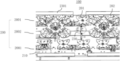
- FIG. 1 is a schematic perspective view showing a portion of an antenna 100 according to some embodiments of the present invention.
- FIG. 2 is a schematic front view showing the portion of the antenna 100 in FIG. 1 .
- FIG. 3 is a schematic end view showing the portion of the antenna 100 in FIG. 1 .
- the antenna 100 may be mounted on a raised structure, such as antenna towers, utility poles, buildings, water towers and the like, with its longitudinal axis extending substantially perpendicular to the ground for convenient operation.
- the antenna 100 is usually mounted within a radome 240 (the radome is only shown in FIG. 3 ) that provides environmental protection.
- the antenna 100 includes a reflector 210 .
- the reflector 210 may include a metal surface that provides a ground plane and reflects electromagnetic waves reaching it, for example, the metal surface redirects the electromagnetic waves for forward propagation.
- the antenna 100 further includes mechanical and electronic components 250 , such as a connector, a cable, a phase shifter, a remote electronic tilt (RET) unit, a duplexer and the like, which are often disposed on a rear side of the reflector 210 .
- mechanical and electronic components 250 such as a connector, a cable, a phase shifter, a remote electronic tilt (RET) unit, a duplexer and the like, which are often disposed on a rear side of the reflector 210 .
- the antenna 100 may further include an antenna array 200 disposed on a front side of the reflector 210 .
- the antenna array 200 may include an array or arrays 2001 of first radiating elements 201 and an array or arrays 2002 of second radiating elements 202 .
- the antenna 100 may be a multi-band antenna.
- the operating frequency band of the first radiating elements 201 may be, for example, V band (1695-2690 MHz) or sub-bands thereof (for example, H band (1695-2200 MHz), T band (2200-2690 MHz), or the like).
- the arrays 2001 of first radiating elements 201 may be configured to generate first antenna beams in the V band or a portion thereof.
- the operating frequency band of the second radiating elements 202 may be, for example, R band (694-960 MHz) or sub-bands thereof.
- the array 2002 of second radiating elements 202 may be configured to generate second antenna beams in the R band or a portion thereof.
- the antenna array 200 may further include an array or arrays of third radiating elements (not shown).
- the operating frequency band of the third radiating elements may be, for example, S band (3.1-4.2 GHz) or sub-bands thereof.
- the array(s) of third radiating elements may be configured to generate third antenna beams in the S band or a portion thereof.
- the antenna 100 may be configured as a so-called RVVSS multi-band antenna. That is, two arrays 2001 of first radiating elements 201 , one array 2002 of second radiating elements 202 and two arrays of third radiating elements are provided.
- the antenna 100 may be any type of antennas (such as beamforming antennas) and is not limited to the current embodiment.
- the antenna array 200 may only include an array or arrays of first radiating elements 2001 .
- the spacing between radiating elements of different arrays 200 typically decreases, which results in increased coupling interference between the arrays 200 .
- This increased coupling interference may degrade the isolation (particularly the Co-polarization or “Co-pol” isolation) of the of radiating elements.
- the coupling interference between the arrays 200 may affect the radiation patterns in both the azimuth and elevation planes. Excessive coupling may affect not only the gain (due to coupling loss), but also may distort the shapes of the radiation patterns, thereby degrading the RF performance, such as the beamforming performance, of the antenna 100 .
- parasitic elements 230 for the antenna array 200 may be mounted on the reflector 210 .
- the parasitic elements 230 may comprise, for example, conductive elements that are mounted forwardly of the reflector 210 and are adjacent to one or more of the radiating elements.
- the parasitic elements 230 may be configured to shape the radiation pattern of the one or more adjacent radiating elements.
- parasitic elements 230 may be designed to narrow or widen the beamwidth of the radiation pattern(s) of the one or more adjacent radiating elements in the azimuth plane.
- the parasitic elements 230 may include fences 2301 that are placed around the antenna array 200 or between adjacent radiating elements.
- parasitic elements 230 may be positioned to act as isolators between adjacent radiating elements to increase the isolation and thereby reduce the coupling interference between the adjacent radiating elements.
- Other parasitic elements 230 may be placed around the antenna array 200 and may interact with the respective radiating elements. For example, in operation, the parasitic elements 230 may receive radio waves emitted by the respective radiating elements and then radiate the radio waves outward in different phases so as to adjust characteristics of the antenna beam of the antenna array 200 , such as the beam width.
- a parasitic element 230 based on a magnetic dipole model is provided. Further, the parasitic element 230 based on the magnetic dipole model may interact with the radiating elements based on an electric dipole model to at least partially compensate for distortion of the radiation pattern of the antenna array 200 caused, for example, by radiating elements of another nearby array.
- a magnetic dipole refers to a physical model established by analogy to the electric dipole.
- a system composed of two points of magnetic charges of equal magnitude and opposite polarity is called a magnetic dipole.
- a commonly used magnetic dipole model may be equivalent to a current loop.
- the electromagnetic properties of the current loop may be represented by an equivalent magnetic current and an equivalent magnetic charge similar to the current element.
- the direction of the equivalent magnetic current and the current direction of the current loop conform to the right-hand screw rule.
- the electric dipole and the magnetic dipole may have good complementary characteristics in the radiation pattern, such as the far-field radiation pattern.
- the far-field radiation pattern in the elevation plane may be approximately circular, and the far-field radiation pattern in the azimuth plane may be approximated to the shape of “8”.
- the far-field radiation pattern in the elevation plane may be approximated to the shape of “8”, and the far-field radiation pattern in the azimuth plane may be approximately circular. Therefore, the selective combination of the electric dipole and the magnetic dipole may improve the symmetry and balance of the radiation pattern in the azimuth plane.
- the parasitic element 230 mounted on the reflector 210 may include a metal ring 231 , thereby forming an equivalent current loop. As shown in FIGS. 1 to 3 , the metal ring 231 of the parasitic element 230 may be arranged between adjacent radiating elements (for example, adjacent first radiating elements 201 ) to function as an isolator for reducing the coupling interference between the adjacent radiating elements.
- adjacent radiating elements for example, adjacent first radiating elements 201
- FIG. 4 is an enlarged schematic view of a parasitic element 230 according to embodiments of the present invention that functions as an isolator.
- the parasitic element 230 may include a support leg 232 and a metal ring 231 mounted on the support leg 232 .
- the support leg 232 is mounted on the reflector 210 .
- the metal ring 231 may be a metal structure or a sheet metal part, such as a copper ring, an aluminum ring or an alloy ring.
- the support leg 232 may be made of a non-conductive material, such as plastic, so that the metal ring 231 may be electrically floating.
- the support leg 232 may be made of metal material, so that the metal ring 231 may be galvanically (or alternatively, capacitively) coupled to the reflector 210 .
- the parasitic element 230 may be mounted on the reflector 210 by means of bayonet connection, screw connection, rivet connection, welding, and/or bonding, for example.
- the parasitic element 230 with a metal ring 231 may be cost-effective; second, may be of any desired thickness; and may have a low level of surface roughness and exhibit improved passive intermodulation (“PIM”) distortion performance.
- PIM passive intermodulation
- the metal ring 231 may also be configured as a trace ring printed on a printed circuit board.
- the parasitic element 230 with a PCB-based metal ring 231 may also be advantageous, because it is easy to print various conductive sections on a printed circuit board, and the implementation of the conductive sections is flexible and diverse so that the conductive sections can be better adapted to the actual application situation.
- the metal ring 231 may be configured as a ring structure of various shapes, such as a circular ring, a polygonal ring, an elliptical ring, or the like.
- the ring may also include both curved and straight segments.
- the specific shape of the metal ring 231 is not limited in this application.
- the metal ring 231 may be configured as a closed ring. In other words, the metal ring 231 has a continuous conductive path. In other embodiments, the metal ring 231 may also be configured as an open ring with a slot. In other words, the metal ring 231 has an intermittent conductive path. For example, when the metal ring 231 is configured as a trace ring printed on a printed circuit board, it is relatively easy and efficient to provide a slot on the metal ring 231 .
- the metal ring 231 may be understood as a metal structure having a metal-free region inside.
- the metal ring 231 may have an outer perimeter 233 with at least 20%, 30%, 40%, 50%, 60%, 70%, 80%, 90% or 95% of the interior of the outer perimeter free of metal.
- the RF performance of the metal ring 231 may be related to the perimeter (outer perimeter, inner perimeter or equivalent perimeter) of the metal ring 231 , particularly to the inner perimeter of metal ring 231 .
- a reference frequency point may be selected so that the perimeter of the metal ring 231 is substantially equal to the reference wavelength corresponding to the reference frequency point.
- the perimeter of the metal ring 231 of the parasitic element 230 may be between 80% and 120% of the reference wavelength.
- the RF performance such as the degree of isolation (inter-band isolation and/or intra-band isolation) at some frequency points, of the radiating element (such as the first radiating element 201 ) within its operating frequency band may be firstly considered. Then, a frequency point with the worst isolation or several frequency points with poor isolation is/are selected. The selected frequency point itself or a frequency point obtained by numerically processing (such as filtering and/or averaging) of the selected several frequency points may be selected as the final reference frequency point.
- the isolation degree (such as the inter-band isolation) of the radiating element within its operating frequency band may be advantageously kept at a good level, for example, below ⁇ 28 dB.
- the dotted line exemplarily shows a characteristic curve of an inter-band isolation of an antenna without a parasitic element according to some embodiments of the present invention
- the solid line exemplarily shows a characteristic curve of an inter-band isolation of an antenna with a parasitic element according to some embodiments of the present invention.
- the operating frequency band of the array of radiating elements includes 1695 MHz to 2690 MHz.
- the worst inter-band isolation degree of the antenna is located at the frequency point of 1915.8 MHz, and by means of the parasitic element of present invention can effectively improve the inter-band isolation in this worst case from ⁇ 26.79 to ⁇ 29.5 dB. It should be understood that in order to obtain a higher isolation, more parasitic elements can be installed appropriately.
- the metal ring 231 of the parasitic element 230 can not only effectively reduce the coupling interference between adjacent radiating elements, but also effectively reduce the coupling interference caused by the reflection of the radome 240 .
- the coupling interference caused by the reflection of the radome 240 is related to the arched configuration of the radome 240 itself, the short distance between the radiating element and the radome 240 , and/or the operating frequency band of the radiating element.
- the metal ring 231 of the parasitic element 230 may extend further from the reflector 210 than the first radiating element 201 (refer to FIG. 3 ).
- the metal ring 231 may be located forwardly of the adjacent first radiating elements 201 , so that the RF signal reflected by the radome 240 may be first absorbed by the metal ring 231 , and then re-radiated outwards with different phases and some extent of attenuation, thereby reducing coupling interference to the radiating element caused by the reflection of the radome 240 .
- the specific arrangement of the parasitic element 230 is not limited in this application.
- the parasitic element 230 with the metal ring 231 may also be arranged at other positions, for example, around the antenna array 200 .
- the first radiating element 201 may extend farther to the front of the reflector 210 than the metal ring 231 of the parasitic element 230 .
Abstract
Description
Claims (20)
Applications Claiming Priority (2)
| Application Number | Priority Date | Filing Date | Title |
|---|---|---|---|
| CN202010417635.7A CN113690581A (en) | 2020-05-18 | 2020-05-18 | Antenna with a shield |
| CN202010417635.7 | 2020-05-18 |
Publications (2)
| Publication Number | Publication Date |
|---|---|
| US20210359406A1 US20210359406A1 (en) | 2021-11-18 |
| US11652288B2 true US11652288B2 (en) | 2023-05-16 |
Family
ID=78511923
Family Applications (1)
| Application Number | Title | Priority Date | Filing Date |
|---|---|---|---|
| US17/233,897 Active 2041-09-10 US11652288B2 (en) | 2020-05-18 | 2021-04-19 | Antenna |
Country Status (2)
| Country | Link |
|---|---|
| US (1) | US11652288B2 (en) |
| CN (1) | CN113690581A (en) |
Families Citing this family (9)
| Publication number | Priority date | Publication date | Assignee | Title |
|---|---|---|---|---|
| WO2022046531A1 (en) | 2020-08-28 | 2022-03-03 | Isco International, Llc | Method and system for mitigating passive intermodulation (pim) by performing polarization adjusting |
| US11502404B1 (en) | 2022-03-31 | 2022-11-15 | Isco International, Llc | Method and system for detecting interference and controlling polarization shifting to mitigate the interference |
| US11476574B1 (en) | 2022-03-31 | 2022-10-18 | Isco International, Llc | Method and system for driving polarization shifting to mitigate interference |
| US11476585B1 (en) | 2022-03-31 | 2022-10-18 | Isco International, Llc | Polarization shifting devices and systems for interference mitigation |
| US11509072B1 (en) | 2022-05-26 | 2022-11-22 | Isco International, Llc | Radio frequency (RF) polarization rotation devices and systems for interference mitigation |
| US11515652B1 (en) | 2022-05-26 | 2022-11-29 | Isco International, Llc | Dual shifter devices and systems for polarization rotation to mitigate interference |
| US11509071B1 (en) | 2022-05-26 | 2022-11-22 | Isco International, Llc | Multi-band polarization rotation for interference mitigation |
| US11949489B1 (en) | 2022-10-17 | 2024-04-02 | Isco International, Llc | Method and system for improving multiple-input-multiple-output (MIMO) beam isolation via alternating polarization |
| US11956058B1 (en) | 2022-10-17 | 2024-04-09 | Isco International, Llc | Method and system for mobile device signal to interference plus noise ratio (SINR) improvement via polarization adjusting/optimization |
Citations (8)
| Publication number | Priority date | Publication date | Assignee | Title |
|---|---|---|---|---|
| US6734829B1 (en) | 1999-07-08 | 2004-05-11 | Kathrein-Werke Kg | Antenna |
| US20040263392A1 (en) * | 2003-06-26 | 2004-12-30 | Bisiules Peter John | Antenna element, feed probe; dielectric spacer, antenna and method of communicating with a plurality of devices |
| US20070146225A1 (en) * | 2005-12-28 | 2007-06-28 | Kathrein-Werke Kg | Dual polarized antenna |
| US20140139387A1 (en) * | 2012-11-22 | 2014-05-22 | Andrew Llc | Ultra-Wideband Dual-Band Cellular Basestation Antenna |
| CN205069883U (en) | 2015-10-27 | 2016-03-02 | 广东健博通科技股份有限公司 | Antenna is transferred to multifrequency section multisystem electricity |
| US20170125917A1 (en) * | 2015-11-02 | 2017-05-04 | Wha Yu Industrial Co., Ltd. | Antenna device and its dipole element with group of loading metal patches |
| US20170346191A1 (en) * | 2014-12-09 | 2017-11-30 | Communication Components Antenna Inc. | Dipole antenna with beamforming ring |
| CN209183753U (en) | 2018-12-29 | 2019-07-30 | 京信通信技术(广州)有限公司 | Mimo antenna array and its antenna-reflected plate |
-
2020
- 2020-05-18 CN CN202010417635.7A patent/CN113690581A/en active Pending
-
2021
- 2021-04-19 US US17/233,897 patent/US11652288B2/en active Active
Patent Citations (8)
| Publication number | Priority date | Publication date | Assignee | Title |
|---|---|---|---|---|
| US6734829B1 (en) | 1999-07-08 | 2004-05-11 | Kathrein-Werke Kg | Antenna |
| US20040263392A1 (en) * | 2003-06-26 | 2004-12-30 | Bisiules Peter John | Antenna element, feed probe; dielectric spacer, antenna and method of communicating with a plurality of devices |
| US20070146225A1 (en) * | 2005-12-28 | 2007-06-28 | Kathrein-Werke Kg | Dual polarized antenna |
| US20140139387A1 (en) * | 2012-11-22 | 2014-05-22 | Andrew Llc | Ultra-Wideband Dual-Band Cellular Basestation Antenna |
| US20170346191A1 (en) * | 2014-12-09 | 2017-11-30 | Communication Components Antenna Inc. | Dipole antenna with beamforming ring |
| CN205069883U (en) | 2015-10-27 | 2016-03-02 | 广东健博通科技股份有限公司 | Antenna is transferred to multifrequency section multisystem electricity |
| US20170125917A1 (en) * | 2015-11-02 | 2017-05-04 | Wha Yu Industrial Co., Ltd. | Antenna device and its dipole element with group of loading metal patches |
| CN209183753U (en) | 2018-12-29 | 2019-07-30 | 京信通信技术(广州)有限公司 | Mimo antenna array and its antenna-reflected plate |
Also Published As
| Publication number | Publication date |
|---|---|
| US20210359406A1 (en) | 2021-11-18 |
| CN113690581A (en) | 2021-11-23 |
Similar Documents
| Publication | Publication Date | Title |
|---|---|---|
| US11652288B2 (en) | Antenna | |
| US11108135B2 (en) | Base station antennas having parasitic coupling units | |
| EP3955383B1 (en) | Multi-band base station antennas having broadband decoupling radiating elements and related radiating elements | |
| US10601120B2 (en) | Base station antennas having reflector assemblies with RF chokes | |
| CN109066073B (en) | Plane end-fire directional diagram reconfigurable antenna | |
| US11575197B2 (en) | Multi-band antenna having passive radiation-filtering elements therein | |
| US20200127389A1 (en) | Antennas including multi-resonance cross-dipole radiating elements and related radiating elements | |
| CN113748572B (en) | Radiating element with angled feed stalk and base station antenna including the same | |
| JP5143911B2 (en) | Dual-polarized radiating element for cellular base station antenna | |
| CN108321535B (en) | Miniaturized low-profile dual-polarized omnidirectional antenna | |
| US20230017375A1 (en) | Radiating element, antenna assembly and base station antenna | |
| JP2003174317A (en) | Multi-band patch antenna and skeleton slot radiator | |
| CN110957569A (en) | Broadband radiation unit and antenna | |
| Zhao et al. | 5G mm-wave antenna array based on T-slot antenna for mobile terminals | |
| US8193997B2 (en) | Directional planar log-spiral slot antenna | |
| Morshed et al. | Dielectric loaded planar inverted-F antenna for millimeter-wave 5G hand held devices | |
| Alieldin et al. | Design of broadband dual-polarized oval-shaped base station antennas for mobile systems | |
| CN113764871A (en) | Low-profile dual-band dual-polarization common-caliber conformal phased array antenna | |
| Morshed et al. | Wideband slotted planar inverted-F antenna for millimeter-wave 5G mobile devices | |
| Ta et al. | A cavity-backed angled-dipole antenna array for low millimeter-wave bands | |
| CN212182536U (en) | Multiband antenna | |
| EP3893328A1 (en) | Multi-band antenna having passive radiation-filtering elements therein | |
| US11437714B2 (en) | Radiating elements having parasitic elements for increased isolation and base station antennas including such radiating elements | |
| CN212182537U (en) | Antenna with a shield | |
| WO2021162961A1 (en) | Patch antenna assembly with grounded posts |
Legal Events
| Date | Code | Title | Description |
|---|---|---|---|
| AS | Assignment |
Owner name: COMMSCOPE TECHNOLOGIES LLC, NORTH CAROLINA Free format text: ASSIGNMENT OF ASSIGNORS INTEREST;ASSIGNORS:YANG, LEI;AI, BIN;LV, FUSHENG;AND OTHERS;REEL/FRAME:055959/0135 Effective date: 20210416 |
|
| FEPP | Fee payment procedure |
Free format text: ENTITY STATUS SET TO UNDISCOUNTED (ORIGINAL EVENT CODE: BIG.); ENTITY STATUS OF PATENT OWNER: LARGE ENTITY |
|
| STPP | Information on status: patent application and granting procedure in general |
Free format text: DOCKETED NEW CASE - READY FOR EXAMINATION |
|
| AS | Assignment |
Owner name: JPMORGAN CHASE BANK, N.A., NEW YORK Free format text: ABL SECURITY AGREEMENT;ASSIGNORS:ARRIS ENTERPRISES LLC;COMMSCOPE TECHNOLOGIES LLC;COMMSCOPE, INC. OF NORTH CAROLINA;REEL/FRAME:058843/0712 Effective date: 20211112 Owner name: JPMORGAN CHASE BANK, N.A., NEW YORK Free format text: TERM LOAN SECURITY AGREEMENT;ASSIGNORS:ARRIS ENTERPRISES LLC;COMMSCOPE TECHNOLOGIES LLC;COMMSCOPE, INC. OF NORTH CAROLINA;REEL/FRAME:058875/0449 Effective date: 20211112 |
|
| AS | Assignment |
Owner name: WILMINGTON TRUST, DELAWARE Free format text: SECURITY INTEREST;ASSIGNORS:ARRIS SOLUTIONS, INC.;ARRIS ENTERPRISES LLC;COMMSCOPE TECHNOLOGIES LLC;AND OTHERS;REEL/FRAME:060752/0001 Effective date: 20211115 |
|
| STPP | Information on status: patent application and granting procedure in general |
Free format text: NON FINAL ACTION MAILED |
|
| STCF | Information on status: patent grant |
Free format text: PATENTED CASE |
|
| CC | Certificate of correction |