US11651613B2 - Fingerprint recognition circuit, driving method therefor, display panel, and display device - Google Patents
Fingerprint recognition circuit, driving method therefor, display panel, and display device Download PDFInfo
- Publication number
- US11651613B2 US11651613B2 US17/288,669 US202017288669A US11651613B2 US 11651613 B2 US11651613 B2 US 11651613B2 US 202017288669 A US202017288669 A US 202017288669A US 11651613 B2 US11651613 B2 US 11651613B2
- Authority
- US
- United States
- Prior art keywords
- signal line
- terminal
- fingerprint recognition
- control
- coupled
- Prior art date
- Legal status (The legal status is an assumption and is not a legal conclusion. Google has not performed a legal analysis and makes no representation as to the accuracy of the status listed.)
- Active, expires
Links
Images


Classifications
-
- G—PHYSICS
- G06—COMPUTING; CALCULATING OR COUNTING
- G06V—IMAGE OR VIDEO RECOGNITION OR UNDERSTANDING
- G06V40/00—Recognition of biometric, human-related or animal-related patterns in image or video data
- G06V40/10—Human or animal bodies, e.g. vehicle occupants or pedestrians; Body parts, e.g. hands
- G06V40/12—Fingerprints or palmprints
- G06V40/13—Sensors therefor
- G06V40/1306—Sensors therefor non-optical, e.g. ultrasonic or capacitive sensing
-
- G—PHYSICS
- G06—COMPUTING; CALCULATING OR COUNTING
- G06V—IMAGE OR VIDEO RECOGNITION OR UNDERSTANDING
- G06V40/00—Recognition of biometric, human-related or animal-related patterns in image or video data
- G06V40/10—Human or animal bodies, e.g. vehicle occupants or pedestrians; Body parts, e.g. hands
- G06V40/12—Fingerprints or palmprints
- G06V40/13—Sensors therefor
- G06V40/1318—Sensors therefor using electro-optical elements or layers, e.g. electroluminescent sensing
Definitions
- the present disclosure relates to the technical field of fingerprint recognition, in particular to a fingerprint recognition circuit, a method for driving the fingerprint recognition circuit, a display panel, and a display device.
- Fingerprint recognition plays a huge role in protecting personal privacy as a biometric recognition method, and almost all current electronic products on the market, such as automobiles, cell phones, and time recorders, are equipped with fingerprint recognition systems.
- the fingerprint recognition technology mainly includes under-screen infrared fingerprint recognition, in-screen capacitive fingerprint recognition, and in-screen optical fingerprint recognition.
- an optical sensor needs to be integrated inside a display device, resulting in a complex circuit structure of the display device and poor fingerprint recognition effects.
- a photosensitive detection circuit coupled to a bias control signal terminal and configured to receive light reflected from a fingerprint and generate a control signal
- a reset control circuit coupled to a reset signal terminal, a first control terminal, and the photosensitive detection circuit respectively, and configured to provide a signal of the reset signal terminal to the photosensitive detection circuit under control of the first control terminal;
- a signal reading circuit coupled to the photosensitive detection circuit, a power supply terminal, a second control terminal, and a signal output terminal respectively, and configured to output a corresponding fingerprint recognition signal based on the control signal under control of the second control terminal.
- the photosensitive detection circuit includes a first capacitor and a photosensitive diode.
- a first electrode of the first capacitor is coupled to a first electrode of the photosensitive diode, and a second electrode of the first capacitor is coupled to a second electrode of the photosensitive diode.
- the second electrode of the photosensitive diode is coupled to the bias control signal terminal.
- the reset control circuit includes a first switch transistor.
- a control terminal of the first switch transistor is coupled to the first control terminal, a first pole of the first switch transistor is coupled to the reset signal terminal, and a second pole of the first switch transistor is coupled to the photosensitive detection circuit.
- the signal reading circuit includes a second switch transistor and a third switch transistor.
- a control terminal of the second switch transistor is coupled to the photosensitive detection circuit, a first pole of the second switch transistor is coupled to the power supply terminal, and a second pole of the second switch transistor is coupled to a first pole of the third switch transistor.
- a control terminal of the third switch transistor is coupled to the second control terminal, and a second pole of the third switch transistor is coupled to the signal output terminal.
- inventions of the present disclosure further provide a display panel.
- the display panel includes a base substrate, a plurality of sub-pixels arranged in an array on the base substrate, and the above-described fingerprint recognition circuit.
- the fingerprint recognition circuit is located in a row gap between adjacent sub-pixels.
- one fingerprint recognition circuit corresponds to one sub-pixel group.
- the sub-pixel group includes two rows and six columns of sub-pixels, and the fingerprint recognition circuit is located in the row gap between the two rows of the sub-pixels in the corresponding sub-pixel group.
- the display panel further includes: a plurality of data signal lines, a reading signal line, a power supply signal line, and a reset signal line.
- the data signal lines, the reading signal line, the power supply signal line, and the reset signal line are extending in a sub-pixel column direction.
- the reading signal line is coupled to the signal output terminal of the fingerprint recognition circuit
- the power supply signal line is coupled to the power supply terminal of the fingerprint recognition circuit
- the reset signal line is coupled to the reset signal terminal of the fingerprint recognition circuit.
- Extension directions of the reading signal line, the power supply signal line and reset signal line coincide with extension directions of the data signal lines.
- the sub-pixel group is provided with six column gaps, and the column gaps each is located on a same side of a respective one of the columns of the sub-pixels.
- the data signal lines, the reading signal line, the power supply signal line, and the reset signal line are all located in the column gaps of the sub-pixel group corresponding to the coupled fingerprint recognition circuit.
- each of the data signal lines is arranged in a respective one of the column gaps in the sub-pixel group.
- the reading signal line, the power supply signal line, and the reset signal line are respectively located in different column gaps.
- only one of the data signal lines is arranged in the second column gap in the sub-pixel group, and only one of the data signal lines is arranged in the fifth column gap in the sub-pixel group.
- each of line widths of the data signal lines in the second and fifth column gaps in the sub-pixel group is larger than each of line widths of the data signal lines in the remaining column gaps.
- the display panel further includes: a suspended signal line located in a column gap.
- the suspended signal line is located in a different column gap from the reading signal line, the power supply signal line, and the reset signal line.
- the display panel further includes: a bias control signal line, a first control signal line, and a second control signal line, the bias control signal line, the first control signal line, and the second control signal line extend in a pixel row direction.
- the bias control signal line is coupled to the bias control signal terminal of the fingerprint recognition circuit, the first control signal line is coupled to the first control terminal of the fingerprint recognition circuit, and the second control signal line is coupled to the second control terminal of the fingerprint recognition circuit.
- the bias control signal line, the first control signal line, and the second control signal line are located in the row gap in the sub-pixel group corresponding to the coupled fingerprint recognition circuit and are arranged on two sides of the fingerprint recognition circuit.
- the bias control signal line and the second control signal line are on a same side of the fingerprint recognition circuit of the row gap, and the first control signal line is on the other side of the fingerprint recognition circuit in the row gap.
- the bias control signal line and the second control signal line are on different film layers.
- embodiments of the present disclosure further provide a display device, and the display device includes the above-described display panel.
- embodiments of the present disclosure further provide a method for driving the fingerprint recognition circuit, and the driving method includes:
- FIG. 1 is a schematic structural diagram of a fingerprint recognition circuit provided by an embodiment of the present disclosure
- FIG. 2 is a timing diagram corresponding to the fingerprint recognition circuit shown in FIG. 1 ;
- FIG. 3 is a schematic structural diagram of a film layer of a display panel provided by an embodiment of the present disclosure
- FIG. 4 is a schematic top view of a stacked structure of a semiconductor layer and a gate conductive layer in an embodiment of the present disclosure
- FIG. 5 a schematic top view of a first conductive layer in an embodiment of the present disclosure
- FIG. 6 is a schematic top view of a stacked structure of a first conductive layer and a second conductive layer in an embodiment of the present disclosure
- FIG. 7 is a schematic top view of a stacked structure of a second conductive layer, a photosensitive detection layer, and a third conductive layer in an embodiment of the present disclosure.
- FIG. 8 is a flow diagram of a method for driving the fingerprint recognition circuit provided by an embodiment of the present disclosure.
- embodiments of the present disclosure provide a fingerprint recognition circuit, a method for driving the fingerprint recognition circuit, a display panel, and a display device.
- Embodiments of the present disclosure provide a fingerprint recognition circuit. As shown in FIG. 1 , the fingerprint recognition circuit includes:
- a photosensitive detection circuit 101 coupled to a bias control signal terminal VB and configured to receive light reflected from a fingerprint and generate a control signal;
- a reset control circuit 102 coupled to a reset signal terminal VR, a first control terminal V 1 , and the photosensitive detection circuit 101 respectively, and configured to provide a signal of the reset signal terminal VR to the photosensitive detection circuit 101 under control of the first control terminal V 1 ;
- a signal reading circuit 103 coupled to the photosensitive detection circuit 101 , a power supply terminal VD, a second control terminal V 2 , and a signal output terminal VO respectively, and configured to output a corresponding fingerprint recognition signal according to the control signal under control of the second control terminal V 2 .
- the photosensitive detection circuit, the reset control circuit, and the signal reading circuit are arranged. Through mutual cooperation of these three circuits, fingerprint recognition with higher detection accuracy can be achieved. Besides, the structure of the fingerprint recognition circuit is simple, thus a fingerprint recognition sensor integrated into a display device will not increase the complexity of a circuit structure in the display device.
- the fingerprint recognition circuit provided by the embodiments of the present disclosure may be integrated in a liquid crystal display device, and in some embodiments, the fingerprint recognition circuit may be arranged in an array substrate of the liquid crystal display device.
- the structure of the fingerprint recognition circuit is simple, the complexity of a circuit structure in the array substrate will not be increased.
- the fingerprint recognition circuit may also be integrated in other display devices, for example, an organic electroluminescent display device, which is not limited here.
- a plurality of fingerprint recognition circuits may be arranged in a display device.
- the fingerprint recognition circuits may convert optical signals into electrical signals after receiving reflected light from a finger, and because the intensity of the reflected light of fingerprint valleys and fingerprint ridges of the finger is different, a fingerprint image may be obtained by detecting fingerprint recognition signals output from the fingerprint recognition circuits.
- FIG. 2 is a timing diagram corresponding to the fingerprint recognition circuit shown in FIG. 1 .
- the operating principle of the fingerprint recognition circuit provided by the embodiments of the present disclosure will now be explained in details with reference to FIGS. 1 and 2 .
- a first control signal v 1 is input to the first control terminal V 1 to provide the signal of the reset signal terminal VR to the photosensitive detection circuit 101
- a bias control signal vb is input to the bias control signal terminal VB so that the photosensitive detection circuit 101 is in a reverse bias state.
- v denotes the control signal generated by the photosensitive detection circuit
- the photosensitive detection circuit 101 converts the received light reflected from the fingerprint into the electrical signal, thereby causing changes of the control signal v.
- the control signal v is reduced by ⁇ v in the figure. Due to the difference in reflectivity between the fingerprint valleys and the fingerprint ridges, the light received by different photosensitive detection circuits 101 is different in intensity, so the changes ⁇ v of the control signals v generated by the different photosensitive detection circuits 101 are different.
- a second control signal v 2 is input to the second control terminal V 2 , and the signal reading circuit 103 outputs a corresponding fingerprint recognition signal based on the control signal v under control of the second control signal v 2 .
- the fingerprint recognition signal is an output signal vo of the signal reading circuit 103 . Due to the difference in reflectivity between the fingerprint valleys and the fingerprint ridges, the control signals v generated by the different photosensitive detection circuits 101 are different, so the fingerprint recognition signals output by the signal reading circuits 103 are different. Therefore, a fingerprint pattern may be obtained based on the fingerprint recognition signals output by the signal reading circuits 103 .
- the photosensitive detection circuit 101 in the fingerprint recognition circuit may include: a first capacitor C and a photosensitive diode E.
- a first electrode c 1 of the first capacitor C is coupled to a first electrode e 1 of the photosensitive diode E, and a second electrode c 2 of the first capacitor C is coupled to a second electrode e 2 of the photosensitive diode E.
- the second electrode e 2 of the photosensitive diode E is coupled to the bias control signal terminal VB.
- the reset control circuit 102 may provide the signal of the reset signal terminal VR to the photosensitive detection circuit 101 under the control of the first control terminal V 1 , so the first capacitor C is charged.
- the reset control circuit 102 stops providing the signal of the reset signal terminal VR to the photosensitive detection circuit 101 , so charging of the first capacitor C is stopped.
- the photosensitive detection circuit 101 receives the light reflected from the fingerprint, the photosensitive diode E converts the optical signal into the electrical signal, changing the current in a loop of the first capacitor C and the photosensitive diode E, and the first capacitor C is enabled to discharge, so the photosensitive detection circuit 101 is enabled to generate the control signal.
- the photosensitive diode E since for the photosensitive diode E in the reverse bias state, a reverse current is greatly increased to form a photocurrent when the photosensitive diode E is illuminated by the light. The greater the intensity of the received light is, the greater the photocurrent formed by the photosensitive diode E is. Therefore, the photosensitive diode E may be controlled to detect the intensity of the light reflected from the fingerprint in the state of reverse bias. Magnitudes of the signals applied to the reset signal terminal VR and the bias control signal terminal VB in the reset time period may be determined based on a specific structure of the photosensitive diode E.
- the signal applied to the reset signal terminal VR is larger than the signal applied to the bias control signal terminal VB.
- an 8V signal may be applied to the reset signal terminal VR and a 3V signal may be applied to the bias control signal terminal VB, thereby maintaining the photosensitive diode E in the reverse bias state.
- the signal applied to the reset signal terminal VR is smaller than the signal applied to the bias control signal terminal VB.
- a 3V signal may be applied to the reset signal terminal VR and an 8V signal may be applied to the bias control signal terminal VB, thereby maintaining the photosensitive diode E in the reverse bias state.
- the photosensitive detection circuit 101 including the first capacitor C and the photosensitive diode E as an example.
- the photosensitive detection circuit 101 may also be composed of other components, which is not limited here.
- the reset control circuit 102 may include: a first switch transistor TFT 1 .
- a control terminal g 1 of the first switch transistor TFT 1 is coupled to the first control terminal V 1 , a first pole s 1 is coupled to the reset signal terminal VR and a second pole d 1 is coupled to the photosensitive detection circuit 101 .
- the second pole d 1 of the first switch transistor TFT 1 may be coupled to the first electrode e 1 of the photosensitive diode E.
- the control terminal g 1 of the above-mentioned first switch transistor TFT 1 is coupled to the first control terminal V 1 , so under control of the first control terminal V 1 , the first pole s 1 and the second pole d 1 of the first switch transistor TFT 1 may be conducted, thereby providing the signal of the reset signal terminal VR to the photosensitive detection circuit 101 .
- the first switch transistor TFT 1 is an N-type transistor, a high level signal may be applied to the control terminal g 1 of the first switch transistor TFT 1 to enable the first pole s 1 and the second pole d 1 of the first switch transistor TFT 1 to be conducted.
- the reset control circuit 102 including the first switch transistor TFT 1 as an example.
- the reset control circuit 102 may also be composed of other components, which is not limited here.
- the signal reading circuit 103 may include: a second switch transistor TFT 2 , and a third switch transistor TFT 3 .
- a control terminal g 2 of the second switch transistor TFT 2 is coupled to the photosensitive detection circuit 101 , a first pole s 2 is coupled to the power supply terminal VD and a second pole d 2 is coupled to a first pole s 3 of the third switch transistor TFT 3 .
- a control terminal g 3 of the third switch transistor TFT 3 is coupled to the second control terminal V 2 and a second pole d 3 is coupled to the signal output terminal VO.
- the control terminal g 2 of the second switch transistor TFT 2 is coupled to the photosensitive detection circuit 101 .
- the control terminal g 2 of the second switch transistor TFT 2 is coupled to the first electrode e 1 of the photosensitive diode E, that is to say, the conduction state of the second switch transistor TFT 2 is controlled by the control signal generated by the photosensitive detection circuit 101 .
- the drain current may be an output current of the second switch transistor TFT 2 at the second pole d 2 and the gate current may be a control current of the second switch transistor TFT 2 at the control terminal g 2 , the control signal generated by the photosensitive detection circuit 101 eventually affects the drain current of the second switch transistor TFT 2 .
- the intensity of the light reflected from the fingerprint received by the photosensitive detection circuit 101 may be obtained, and by reading drain currents of second switch transistors TFT 2 of a plurality of fingerprint recognition circuits, the fingerprint pattern of the finger may be obtained.
- the control terminal g 3 of the third switch transistor TFT 3 is coupled to the second control terminal V 2 and the second pole d 3 is coupled to the signal output terminal VO.
- the third switch transistor TFT 3 may be conducted by inputting the second control signal v 2 to the second control terminal V 2 , thereby conducting the second pole d 2 of the second switch transistor TFT 2 and the signal output terminal VO, and the signal output terminal VO outputs the fingerprint recognition signal corresponding to the control signal.
- the signal reading circuit 103 including the second switch transistor TFT 2 and the third switch transistor TFT 3 as an example.
- the signal reading circuit 103 may also be composed of other components, which is not limited here.
- embodiments of the present disclosure further provide a display panel. Since the problem solving principle of the display panel is similar to that of the above-described fingerprint recognition circuit, implementation of the display device can be referred to the implementation of the fingerprint recognition circuit, and the repetition thereof will not be described.
- the display panel provided by the embodiments of the present disclosure may include: a base substrate (not shown), a plurality of sub-pixels arranged in an array (e.g., P_ 11 , P_ 12 , P_ 13 , etc. in the figure) on the base substrate, and the fingerprint recognition circuit 10 described above.
- the fingerprint recognition circuit 10 is located in a row gap X between the adjacent sub-pixels.
- the fingerprint recognition circuit is arranged on the base substrate and is integrated into the display panel, so a fingerprint pattern of a finger touching the display panel may be obtained through a fingerprint recognition signal output by the fingerprint recognition circuit.
- the fingerprint recognition circuit is simple in structure, so the complexity of a circuit structure in the display panel will not be increased.
- the fingerprint recognition circuit is arranged in the row gap between the adjacent sub-pixels so it does not occupy opening areas of the sub-pixels, i.e., the display effect of the display panel is not affected.
- Signal lines coupled to the fingerprint recognition circuit may be arranged in column gaps between the sub-pixels, which facilitates routing design of the signal lines.
- a plurality of fingerprint recognition circuits may be arranged in a fingerprint recognition area of the display panel, and through fingerprint recognition signals output from the fingerprint recognition circuits, a complete fingerprint pattern may be obtained by using an image splicing technology.
- the fingerprint recognition area may be a part of a display area of the display panel, or the fingerprint recognition area may coincide with the display area, i.e., the display panel in the embodiments of the present disclosure may realize a partial-area fingerprint recognition function or may realize a full-screen fingerprint recognition function, where the size of the fingerprint recognition area is not defined.
- one fingerprint recognition circuit 10 corresponds to one sub-pixel group, and the sub-pixels in FIG. 3 , i.e. P_ 11 , P_ 12 , P_ 13 , P_ 14 , P_ 15 , P_ 16 , P_ 21 , P_ 22 , P_ 23 , P_ 24 , P_ 25 , and P_ 26 , may constitute one sub-pixel group.
- the sub-pixel group includes two rows and six columns of sub-pixels (each sub-pixel being distributed in the two rows and six columns as shown in FIG. 3 ) and the fingerprint recognition circuit 10 is located in the row gap X between the two rows of sub-pixels in the corresponding sub-pixel group.
- the display panel may include at least three colors of sub-pixels.
- the display panel may include sub-pixels of three colors of red, green, and blue.
- each sub-pixel group may correspond to 2 ⁇ 2 pixel units. As shown in FIG.
- the first row of sub-pixels P_ 11 , P_ 12 , P_ 13 , P_ 14 , P_ 15 , and P_ 16 may be arranged in the order of red, green, blue, red, green, and blue
- the second row of sub-pixels P_ 21 , P_ 22 , P_ 23 , P_ 24 , P_ 25 , and P_ 26 may be arranged in the order of red, green, blue, red, green, and blue.
- the embodiments of the present disclosure further include a plurality of pixel electrodes W.
- each fingerprint recognition circuit 10 corresponds to 2 ⁇ 2 pixel units, so fingerprint recognition accuracy may be satisfied, and a clear fingerprint pattern may be obtained. Furthermore, the fingerprint recognition circuit 10 is arranged in the row gap X between two rows of sub-pixels in the corresponding sub-pixel group, so it does not occupy opening areas of the sub-pixels, i.e., the display effect of the display panel is not affected. Besides, signal lines coupled to the fingerprint recognition circuit may be arranged in column gaps between the sub-pixels, which facilitates routing design of the signal lines.
- the above-described display panel provided by the embodiments of the present disclosure may further include: a plurality of data signal lines (shown as D 1 , D 2 , D 3 , D 4 , D 5 , and D 6 in FIG. 3 ) extending in the column direction of the sub-pixels, a reading signal line 401 , a power supply signal line 402 , and a reset signal line 403 .
- the reading signal line 401 is coupled to the signal output terminal VO of the fingerprint recognition circuit 10
- the power supply signal line 402 is coupled to the power supply terminal VD of the fingerprint recognition circuit 10
- the reset signal line 403 is coupled to the reset signal terminal VR of the fingerprint recognition circuit 10 .
- the extension directions of the reading signal line 401 , the power supply signal line 402 , and the reset signal line 403 coincide with the extension directions of the data signal lines.
- the sub-pixel group has six column gaps (column gaps Y 1 , Y 2 , Y 3 , Y 4 , Y 5 , and Y 6 in FIG. 3 ) which are located on the same side of the columns of sub-pixels, and as shown in the figure, each column gap is located on the left side of the corresponding column of sub-pixels.
- the data signal lines, the reading signal line 401 , the power supply signal line 402 , and the reset signal line 403 are positioned in the column gaps of the sub-pixel group corresponding to the coupled fingerprint recognition circuit 10 .
- the reading signal line 401 , the power supply signal line 402 , and the reset signal line 403 are arranged in the column gaps of the sub-pixel group corresponding to the coupled fingerprint recognition circuit 10 , thereby facilitating coupling with the corresponding fingerprint recognition circuit 10 , and they do not occupy the opening areas of the sub-pixels, i.e., the display effect of the display panel is not affected.
- the data signal lines, the reading signal line 401 , the power supply signal line 402 , and the reset signal line 403 may be located on a same film layer. For example, they may be all located on a first conductive layer 40 .
- FIG. 5 is a schematic structural diagram of the first conductive layer 40 . As shown in FIGS. 3 and 5 , one data signal line is arranged in each column gap in the sub-pixel group. As shown in FIG.
- a data signal line D 1 is located in the column gap Y 1
- a data signal line D 2 is located in the column gap Y 2
- a data signal line D 3 is located in the column gap Y 3
- a data signal line D 4 is located in the column gap Y 4
- a data signal line D 5 is located in the column gap Y 5
- a data signal line D 6 is located in the column gap Y 6 , thereby facilitating coupling of the data signal lines to the sub-pixels in the corresponding sub-pixel columns. Therefore, the data signal lines provide data signals to the coupled sub-pixels, and signal crosstalk between the adjacent data signal lines may be avoided, thereby ensuring the good display effect of the display panel.
- the reading signal line 401 , the power supply signal line 402 , and the reset signal line 403 are located in different column gaps, which can avoid signal crosstalk between the reading signal line 401 , the power supply signal line 402 , and the reset signal line 403 and guarantee high fingerprint recognition accuracy of the fingerprint recognition circuit.
- only one data signal line is arranged in each of the second and fifth column gaps (i.e., the column gap Y 2 and the column gap Y 5 ) in the sub-pixel group, that is, no signal line except the data signal line D 2 is arranged in the column gap Y 2 and no signal line except the data signal line D 5 is arranged in the column gap Y 5 .
- the reading signal line 401 , the power supply signal line 402 , and the reset signal line 403 are distributed in the column gaps Y 1 , Y 4 , and Y 6 , so that the reading signal line 401 , the power supply signal line 402 , and the reset signal line 403 are evenly distributed in the column gaps of the corresponding sub-pixel group.
- line widths of the data signal lines in the second and fifth column gaps in the sub-pixel group are larger than line widths of the data signal lines in the remaining column gaps, i.e., the line widths of the data signal lines D 2 and D 5 are larger than those of the data signal lines D 1 , D 3 , D 4 , and D 6 . Since only one data signal line is arranged in the column gap Y 2 and in the column gap Y 5 respectively, there is sufficient space in the column gap Y 2 and the column gap Y 5 , and the line widths of the data signal lines D 2 and D 5 are large, thereby achieving small resistance of the data signal lines D 2 and D 5 .
- the total width of the vertical signal line in each of the column gaps Y 2 and Y 5 may be consistent with the total width of the vertical signal line in each of the remaining column gaps, thereby improving the uniformity of the vertical signal lines in the column gaps corresponding to the sub-pixel group, resulting in good display uniformity of the display panel.
- the above-described display panel provided by the embodiments of the present disclosure may further include: a suspended signal line 404 located in a column gap.
- the suspended signal line 404 is located in the column gap different from those of the reading signal line 401 , the power supply signal line 402 , and the reset signal line 403 .
- the reading signal line 401 is located in the column gap Y 1
- the suspended signal line 404 is located in the column gap Y 3
- the power supply signal line 402 is located in the column gap Y 4
- the reset signal line 403 is located in the column gap Y 6 .
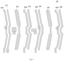
- FIG. 4 is a schematic top view of a stacked structure of a semiconductor layer 20 and a gate conductive layer 30
- FIG. 5 is a schematic top view of the first conductive layer 40
- FIG. 6 is a schematic top view of a stacked structure of the first conductive layer 40 and a second conductive layer 50
- FIG. 7 is a schematic top view of a stacked structure of the second conductive layer 50 , a photosensitive detection layer 60 , and a third conductive layer 70 .
- FIGS. 4 is a schematic top view of a stacked structure of a semiconductor layer 20 and a gate conductive layer 30
- FIG. 5 is a schematic top view of the first conductive layer 40
- FIG. 6 is a schematic top view of a stacked structure of the first conductive layer 40 and a second conductive layer 50
- FIG. 7 is a schematic top view of a stacked structure of the second conductive layer 50 , a photosensitive detection layer 60 , and a third conductive layer 70 .
- the stacking order of the respective film layers in the display panel is the semiconductor layer 20 , the gate conductive layer 30 , the first conductive layer 40 , the second conductive layer 50 , the photosensitive detection layer 60 , and the third conductive layer 70 from bottom to top in sequence.
- the above-described display panel provided by the embodiments of the present disclosure may further include: a first control signal line 301 , and a second control signal line 302 , and a bias control signal line 701 extending in the pixel row direction.
- the bias control signal line 701 is coupled to the bias control signal terminal VB of the fingerprint recognition circuit 10
- the first control signal line 301 is coupled to the first control terminal of the fingerprint recognition circuit 10
- the second control signal line 302 is coupled to the second control terminal of the fingerprint recognition circuit 10 .
- the first control signal line 301 and the second control signal line 302 are both located in the gate conductive layer 30 , and the gate conductive layer 30 may further include: the control terminal g 1 of the first switch transistor TFT 1 , the control terminal g 2 of the second switch transistor TFT 2 , and the control terminal g 3 of the third switch transistor TFT 3 .
- the region where the control terminal g 1 overlaps the semiconductor layer 20 is a channel region of the first switch transistor TFT 1 , conductive regions on both sides of the channel region of the first switch transistor TFT 1 are the first pole s 1 and the second pole d 1 respectively, the region where the control terminal g 2 overlaps the semiconductor layer 20 is a channel region of the second switch transistor TFT 2 , conductive regions on both sides of the channel region of the second switch transistor TFT 2 are the first pole s 2 and the second pole d 2 respectively, the region where the control terminal g 3 overlaps the semiconductor layer 20 is a channel region of the third switch transistor TFT 3 , and conductive regions on both sides of the channel region of the third switch transistor TFT 3 are the first pole s 3 and the second pole d 3 respectively.
- the first control signal line 301 is coupled to the first control terminal of the fingerprint recognition circuit 10 , i.e. the first control signal line 301 is coupled to the control terminal g 1 of the first switch transistor TFT 1 .
- the second control signal line 302 is coupled to the second control terminal of the fingerprint recognition circuit 10 , i.e. the second control signal line 302 is coupled to the control terminal g 3 of the third switch transistor TFT 3 .
- the first pole s 3 of the third switch transistor TFT 3 is coupled to the second pole d 2 of the second switch transistor TFT 2
- the control terminal g 2 of the second switch transistor TFT 2 is coupled to the second pole d 1 of the first switch transistor TFT 1 .
- the control terminal g 1 , the control terminal g 2 , and the control terminal g 3 may be of a dual gate structure.
- the second conductive layer 50 may include: a first conductive part 501 and a touch signal line 502 .
- the first conductive part 501 can serve as the first electrode c 1 of the first capacitor C and the first electrode e 1 of the photosensitive diode E.
- the first conductive part 501 is located in the row gap between the sub-pixels and the touch signal line 502 is located in the column gaps between the sub-pixels, which will not affect the opening ratio of the sub-pixels and can guarantee the display effect of the display panel.
- an area 601 in the photosensitive detection layer 60 represents the position where a photosensitive semiconductor layer in the photosensitive diode E is located.
- the photosensitive semiconductor layer 601 may include a first semiconductor layer, an intrinsic semiconductor layer, and a second semiconductor layer which are stacked.
- the first semiconductor layer is an N-type semiconductor layer and the second semiconductor layer is a P-type semiconductor layer, or the first semiconductor layer is a P-type semiconductor layer and the second semiconductor layer is an N-type semiconductor layer.
- a transparent conductive layer may also be arranged on the photosensitive semiconductor layer 601 .
- the transparent conductive layer may be made of a transparent conductive oxide such as indium tin oxide (ITO).
- ITO indium tin oxide
- a pattern of the transparent conductive layer may coincide with the photosensitive semiconductor layer 601 in position.
- the pattern of the transparent conductive layer may serve as the second electrode c 2 of the first capacitor C and the second electrode e 2 of the photosensitive diode E.
- the arrangement of the transparent conductive layer on the photosensitive semiconductor layer 601 does not affect the photosensitive detection circuit in receiving the reflected light from the fingerprint, so the fingerprint detection effect is not affected.
- the third conductive layer 70 includes the bias control signal line 701 which is coupled to the pattern of the transparent conductive layer, i.e., the bias control signal line 701 is coupled to the photosensitive detection circuit so that a bias control signal may be provided to the photosensitive detection circuit.
- the bias control signal line 701 , the first control signal line 301 , and the second control signal line 302 are located in the row gap X in the sub-pixel group corresponding to the coupled fingerprint recognition circuit 10 and arranged on two sides of the fingerprint recognition circuit 10 .
- the bias control signal line 701 , the first control signal line 301 , and the second control signal line 302 do not occupy the opening areas of the sub-pixels, so the display effect of the display panel is not affected.
- the bias control signal line 701 , the first control signal line 301 , and the second control signal line 302 are arranged on the two sides of the fingerprint recognition circuit 10 to facilitate coupling to a signal terminal in the fingerprint recognition circuit 10 , thereby allowing reasonable utilization of space in the display area.
- the bias control signal line 701 and the second control signal line 302 are located on the same side in the row gap X, and the first control signal line 301 is located on the other side in the row gap X, so that three signal lines extending in the sub-pixel row direction are distributed on both sides in the row gap X and the space in the row gap X may be reasonably utilized. Besides, the three signal lines may be easily coupled to the signal terminal in the fingerprint recognition circuit 10 .
- the bias control signal line 701 and the second control signal line 302 are on different film layers to avoid shorting between the bias control signal line 701 and the second control signal line 302 .
- the first control signal line 301 and the second control signal line 302 may be on the same layer, e.g., they can both be located in the gate conductive layer 30 and the bias control signal line 701 may be located in the third conductive layer 70 .
- embodiments of the present disclosure further provide a display device including the above-described display panel.
- the display device may be applied to any product or component having a display function, such as a mobile phone, a tablet, a television, a display, a laptop, a digital photo frame, and a navigator. Since the problem solving principle of the display device is similar to that of the above-described display panel, implementation of the display device may be referred to the implementation of the above-described display panel, and the repetition thereof will not be described.
- embodiments of the present disclosure further provide a method for driving the above fingerprint recognition circuit. Since the problem solving principle of the driving method is similar to that of the above-described fingerprint recognition circuit, implementation of the driving method may be referred to the implementation of the above-described fingerprint recognition circuit, and the repetition thereof will not be described.
- the method for driving the fingerprint recognition circuit includes the following steps.
- a first control signal is input to a first control terminal to provide a signal of a reset signal terminal to a photosensitive detection circuit, and a bias control signal is input to a bias control signal terminal so the photosensitive detection circuit is in a state of reverse bias.
- a second control signal is input to a second control terminal so that a signal reading circuit outputs a corresponding fingerprint recognition signal based on the control signal under control of the second control signal.
- step S 801 in the reset time period T 1 , the first control signal v 1 is input to the first control terminal V 1 , the bias control signal vb is input to the bias control signal terminal VB, and the reset signal vr is input to the reset signal terminal VR, such that the reset control circuit 102 provides the reset signal vr to the photosensitive detection circuit 101 under the control of the first control signal v 1 , thereby bringing the photosensitive detection circuit 101 into the state of reverse bias.
- step S 802 in the detection time period T 2 , inputting of the first control signal v 1 to the first control terminal V 1 is stopped so each photosensitive detection circuit 101 in a display device receives the light reflected from the fingerprint at the same bias reference.
- v denotes the control signal generated by the photosensitive detection circuit
- the photosensitive detection circuit 101 converts the received light reflected from the fingerprint into an electrical signal, thereby causing changes of the control signal v.
- the control signal v is reduced by ⁇ v in the figure. Due to the difference in reflectivity between fingerprint valleys and fingerprint ridges, the light received by different photosensitive detection circuits 101 is different in intensity, so the changes ⁇ v of the control signals v generated by the different photosensitive detection circuits 101 are different.
- step S 803 in the signal output time period T 3 , the second control signal v 2 is input to the second control terminal V 2 , and the signal reading circuit 103 outputs the corresponding fingerprint recognition signal based on the control signal v under control of the second control signal v 2 .
- the fingerprint recognition signal is an output signal vo of the signal reading circuit 103 . Due to the difference in reflectivity between the fingerprint valleys and the fingerprint ridges, the control signals v generated by the different photosensitive detection circuits 101 are different, so the fingerprint recognition signals output by the signal reading circuits 103 are different. Therefore, a fingerprint pattern may be obtained based on the fingerprint recognition signals output by the signal reading circuits 103 .
- the method for driving the fingerprint recognition circuit, the display panel and the displace device provided by the embodiments of the present disclosure, the photosensitive detection circuit, the reset control circuit, and the signal reading circuit are arranged. Through mutual cooperation of these three circuits, fingerprint recognition with high detection accuracy may be achieved. Besides, the structure of the fingerprint recognition circuit is simple, thus a fingerprint recognition sensor integrated into the display device will not increase the complexity of the circuit structure in the display device.
Abstract
Description
Claims (13)
Applications Claiming Priority (1)
| Application Number | Priority Date | Filing Date | Title |
|---|---|---|---|
| PCT/CN2020/114884 WO2022052061A1 (en) | 2020-09-11 | 2020-09-11 | Fingerprint recognition circuit, driving method therefor, display panel, and display device |
Publications (2)
| Publication Number | Publication Date |
|---|---|
| US20220309820A1 US20220309820A1 (en) | 2022-09-29 |
| US11651613B2 true US11651613B2 (en) | 2023-05-16 |
Family
ID=80630236
Family Applications (1)
| Application Number | Title | Priority Date | Filing Date |
|---|---|---|---|
| US17/288,669 Active 2041-02-14 US11651613B2 (en) | 2020-09-11 | 2020-09-11 | Fingerprint recognition circuit, driving method therefor, display panel, and display device |
Country Status (3)
| Country | Link |
|---|---|
| US (1) | US11651613B2 (en) |
| CN (1) | CN114616601A (en) |
| WO (1) | WO2022052061A1 (en) |
Citations (10)
| Publication number | Priority date | Publication date | Assignee | Title |
|---|---|---|---|---|
| JP2013069201A (en) | 2011-09-26 | 2013-04-18 | Seiko Epson Corp | Optical sensor, driving method thereof, vein sensor and fingerprint sensor |
| CN106250888A (en) | 2016-09-19 | 2016-12-21 | 汕头超声显示器(二厂)有限公司 | A kind of fingerprint recognition induction apparatus with large area identification region and application thereof |
| CN106971172A (en) | 2017-04-13 | 2017-07-21 | 京东方科技集团股份有限公司 | A kind of fingerprint recognition detection circuit, touch-screen and display device |
| CN108062540A (en) | 2018-01-05 | 2018-05-22 | 京东方科技集团股份有限公司 | fingerprint recognition detection circuit and its driving method, display panel and display device |
| CN108280432A (en) | 2018-01-25 | 2018-07-13 | 京东方科技集团股份有限公司 | Fingerprint recognition detection circuit and its driving method, display device |
| US20180300527A1 (en) | 2017-04-13 | 2018-10-18 | Boe Technology Group Co., Ltd. | Fingerprint identification detection circuit, touch screen and display device |
| CN110929667A (en) | 2019-11-29 | 2020-03-27 | 厦门天马微电子有限公司 | Display panel and display device |
| CN111553325A (en) | 2020-05-26 | 2020-08-18 | 上海天马微电子有限公司 | Fingerprint identification circuit, driving method and display device |
| US20220050984A1 (en) * | 2020-08-14 | 2022-02-17 | Samsung Display Co., Ltd. | Input sensing method and input sensing device including the same |
| US20220320050A1 (en) * | 2020-06-16 | 2022-10-06 | Wuhan China Star Optoelectronics Technology Co., Ltd. | Display panel and display device |
-
2020
- 2020-09-11 US US17/288,669 patent/US11651613B2/en active Active
- 2020-09-11 WO PCT/CN2020/114884 patent/WO2022052061A1/en active Application Filing
- 2020-09-11 CN CN202080001925.1A patent/CN114616601A/en active Pending
Patent Citations (10)
| Publication number | Priority date | Publication date | Assignee | Title |
|---|---|---|---|---|
| JP2013069201A (en) | 2011-09-26 | 2013-04-18 | Seiko Epson Corp | Optical sensor, driving method thereof, vein sensor and fingerprint sensor |
| CN106250888A (en) | 2016-09-19 | 2016-12-21 | 汕头超声显示器(二厂)有限公司 | A kind of fingerprint recognition induction apparatus with large area identification region and application thereof |
| CN106971172A (en) | 2017-04-13 | 2017-07-21 | 京东方科技集团股份有限公司 | A kind of fingerprint recognition detection circuit, touch-screen and display device |
| US20180300527A1 (en) | 2017-04-13 | 2018-10-18 | Boe Technology Group Co., Ltd. | Fingerprint identification detection circuit, touch screen and display device |
| CN108062540A (en) | 2018-01-05 | 2018-05-22 | 京东方科技集团股份有限公司 | fingerprint recognition detection circuit and its driving method, display panel and display device |
| CN108280432A (en) | 2018-01-25 | 2018-07-13 | 京东方科技集团股份有限公司 | Fingerprint recognition detection circuit and its driving method, display device |
| CN110929667A (en) | 2019-11-29 | 2020-03-27 | 厦门天马微电子有限公司 | Display panel and display device |
| CN111553325A (en) | 2020-05-26 | 2020-08-18 | 上海天马微电子有限公司 | Fingerprint identification circuit, driving method and display device |
| US20220320050A1 (en) * | 2020-06-16 | 2022-10-06 | Wuhan China Star Optoelectronics Technology Co., Ltd. | Display panel and display device |
| US20220050984A1 (en) * | 2020-08-14 | 2022-02-17 | Samsung Display Co., Ltd. | Input sensing method and input sensing device including the same |
Also Published As
| Publication number | Publication date |
|---|---|
| WO2022052061A1 (en) | 2022-03-17 |
| CN114616601A (en) | 2022-06-10 |
| US20220309820A1 (en) | 2022-09-29 |
Similar Documents
| Publication | Publication Date | Title |
|---|---|---|
| US11009747B2 (en) | Backlight module and display device | |
| US10705648B2 (en) | Pixel circuit, array substrate, display panel, display device and display driving method | |
| US10714506B2 (en) | Photodetector and driving method thereof, display panel and display device | |
| US5446564A (en) | Liquid crystal display device having photosensor at each pixel | |
| US11974462B2 (en) | Display panel and display device | |
| US20210167134A1 (en) | Photosensitive touch substrate, fabrication method thereof and display apparatus | |
| CN104914602B (en) | Display device and array substrate | |
| US10627940B2 (en) | Touch substrate and display device | |
| US11100304B2 (en) | Display panel, driving method, and display device | |
| JP2014099216A (en) | Device having touch sensor, and display device | |
| CN105720037A (en) | Semiconductor device and display device | |
| US10025416B2 (en) | Display panel and method for forming the same | |
| US20210405410A1 (en) | Display substrate and display device | |
| US11296155B2 (en) | Display panel and operation method thereof | |
| EP4002480A1 (en) | Display substrate, and display device | |
| WO2020238839A1 (en) | Texture detection circuit, charging circuit, driving method and touch control display panel | |
| WO2021243880A1 (en) | Display substrate and display apparatus | |
| US10719153B2 (en) | Display panel including touch circuit, touch detection method thereof and display device | |
| CN109983528B (en) | Shift register circuit, driving circuit, display device and driving method | |
| CN108878481B (en) | Display panel and display device | |
| US20230252922A1 (en) | Display module, crack detection method, and display apparatus | |
| US10705646B2 (en) | Touch display panel, method for driving the same, and display device | |
| US11651613B2 (en) | Fingerprint recognition circuit, driving method therefor, display panel, and display device | |
| KR20100009213A (en) | Electro-phoresis display device and the array substrate | |
| US8664581B2 (en) | Input/output device and driving method thereof |
Legal Events
| Date | Code | Title | Description |
|---|---|---|---|
| AS | Assignment |
Owner name: BOE TECHNOLOGY GROUP CO., LTD., CHINA Free format text: ASSIGNMENT OF ASSIGNORS INTEREST;ASSIGNORS:MU, WENKAI;LIU, YI;YANG, XINLAN;AND OTHERS;REEL/FRAME:056038/0149 Effective date: 20210402 Owner name: BEIJING BOE DISPLAY TECHNOLOGY CO., LTD., CHINA Free format text: ASSIGNMENT OF ASSIGNORS INTEREST;ASSIGNORS:MU, WENKAI;LIU, YI;YANG, XINLAN;AND OTHERS;REEL/FRAME:056038/0149 Effective date: 20210402 |
|
| FEPP | Fee payment procedure |
Free format text: ENTITY STATUS SET TO UNDISCOUNTED (ORIGINAL EVENT CODE: BIG.); ENTITY STATUS OF PATENT OWNER: LARGE ENTITY |
|
| STPP | Information on status: patent application and granting procedure in general |
Free format text: DOCKETED NEW CASE - READY FOR EXAMINATION |
|
| STPP | Information on status: patent application and granting procedure in general |
Free format text: NON FINAL ACTION MAILED |
|
| STPP | Information on status: patent application and granting procedure in general |
Free format text: RESPONSE TO NON-FINAL OFFICE ACTION ENTERED AND FORWARDED TO EXAMINER |
|
| STCF | Information on status: patent grant |
Free format text: PATENTED CASE |