EP4002480A1 - Display substrate, and display device - Google Patents
Display substrate, and display device Download PDFInfo
- Publication number
- EP4002480A1 EP4002480A1 EP21773274.2A EP21773274A EP4002480A1 EP 4002480 A1 EP4002480 A1 EP 4002480A1 EP 21773274 A EP21773274 A EP 21773274A EP 4002480 A1 EP4002480 A1 EP 4002480A1
- Authority
- EP
- European Patent Office
- Prior art keywords
- signal line
- light
- display region
- pixel circuit
- display
- Prior art date
- Legal status (The legal status is an assumption and is not a legal conclusion. Google has not performed a legal analysis and makes no representation as to the accuracy of the status listed.)
- Pending
Links
- 239000000758 substrate Substances 0.000 title claims abstract description 179
- 238000005452 bending Methods 0.000 claims abstract description 35
- 238000004804 winding Methods 0.000 claims abstract description 34
- 238000007667 floating Methods 0.000 claims abstract description 4
- 229910052751 metal Inorganic materials 0.000 claims description 66
- 239000002184 metal Substances 0.000 claims description 66
- 239000010409 thin film Substances 0.000 claims description 21
- 239000010408 film Substances 0.000 claims description 10
- 241001270131 Agaricus moelleri Species 0.000 claims description 6
- 239000010410 layer Substances 0.000 description 140
- 239000003990 capacitor Substances 0.000 description 20
- 238000010586 diagram Methods 0.000 description 11
- 238000009826 distribution Methods 0.000 description 10
- 238000003860 storage Methods 0.000 description 10
- 238000005538 encapsulation Methods 0.000 description 9
- 238000002834 transmittance Methods 0.000 description 9
- 239000000463 material Substances 0.000 description 8
- 238000004519 manufacturing process Methods 0.000 description 7
- 238000000034 method Methods 0.000 description 7
- 239000010936 titanium Substances 0.000 description 6
- 239000002096 quantum dot Substances 0.000 description 5
- 101100041125 Arabidopsis thaliana RST1 gene Proteins 0.000 description 4
- 101100443250 Saccharomyces cerevisiae (strain ATCC 204508 / S288c) DIG1 gene Proteins 0.000 description 4
- 101100443251 Saccharomyces cerevisiae (strain ATCC 204508 / S288c) DIG2 gene Proteins 0.000 description 4
- 101100041128 Schizosaccharomyces pombe (strain 972 / ATCC 24843) rst2 gene Proteins 0.000 description 4
- RTAQQCXQSZGOHL-UHFFFAOYSA-N Titanium Chemical compound [Ti] RTAQQCXQSZGOHL-UHFFFAOYSA-N 0.000 description 4
- 229910052782 aluminium Inorganic materials 0.000 description 4
- XAGFODPZIPBFFR-UHFFFAOYSA-N aluminium Chemical compound [Al] XAGFODPZIPBFFR-UHFFFAOYSA-N 0.000 description 4
- 239000011229 interlayer Substances 0.000 description 4
- 229910052719 titanium Inorganic materials 0.000 description 4
- 230000000694 effects Effects 0.000 description 3
- 239000007769 metal material Substances 0.000 description 3
- 230000003287 optical effect Effects 0.000 description 3
- 230000002093 peripheral effect Effects 0.000 description 3
- 239000004065 semiconductor Substances 0.000 description 3
- 101100301524 Drosophila melanogaster Reg-5 gene Proteins 0.000 description 2
- ZOKXTWBITQBERF-UHFFFAOYSA-N Molybdenum Chemical compound [Mo] ZOKXTWBITQBERF-UHFFFAOYSA-N 0.000 description 2
- XLOMVQKBTHCTTD-UHFFFAOYSA-N Zinc monoxide Chemical compound [Zn]=O XLOMVQKBTHCTTD-UHFFFAOYSA-N 0.000 description 2
- 239000000956 alloy Substances 0.000 description 2
- 238000005516 engineering process Methods 0.000 description 2
- 238000005530 etching Methods 0.000 description 2
- 238000002347 injection Methods 0.000 description 2
- 239000007924 injection Substances 0.000 description 2
- 239000011810 insulating material Substances 0.000 description 2
- 239000002346 layers by function Substances 0.000 description 2
- 239000011777 magnesium Substances 0.000 description 2
- 229910052750 molybdenum Inorganic materials 0.000 description 2
- 239000011733 molybdenum Substances 0.000 description 2
- 239000011368 organic material Substances 0.000 description 2
- -1 polyphthalimide Polymers 0.000 description 2
- 238000002360 preparation method Methods 0.000 description 2
- 230000000750 progressive effect Effects 0.000 description 2
- VYPSYNLAJGMNEJ-UHFFFAOYSA-N silicon dioxide Inorganic materials O=[Si]=O VYPSYNLAJGMNEJ-UHFFFAOYSA-N 0.000 description 2
- 239000002356 single layer Substances 0.000 description 2
- 239000000243 solution Substances 0.000 description 2
- KXGFMDJXCMQABM-UHFFFAOYSA-N 2-methoxy-6-methylphenol Chemical compound [CH]OC1=CC=CC([CH])=C1O KXGFMDJXCMQABM-UHFFFAOYSA-N 0.000 description 1
- MARUHZGHZWCEQU-UHFFFAOYSA-N 5-phenyl-2h-tetrazole Chemical class C1=CC=CC=C1C1=NNN=N1 MARUHZGHZWCEQU-UHFFFAOYSA-N 0.000 description 1
- 239000004925 Acrylic resin Substances 0.000 description 1
- 229920000178 Acrylic resin Polymers 0.000 description 1
- 102100023882 Endoribonuclease ZC3H12A Human genes 0.000 description 1
- 101710112715 Endoribonuclease ZC3H12A Proteins 0.000 description 1
- GYHNNYVSQQEPJS-UHFFFAOYSA-N Gallium Chemical compound [Ga] GYHNNYVSQQEPJS-UHFFFAOYSA-N 0.000 description 1
- 101001096074 Homo sapiens Regenerating islet-derived protein 4 Proteins 0.000 description 1
- 101000639970 Homo sapiens Sodium- and chloride-dependent GABA transporter 1 Proteins 0.000 description 1
- 101001094079 Homo sapiens Sodium- and chloride-dependent GABA transporter 2 Proteins 0.000 description 1
- GPXJNWSHGFTCBW-UHFFFAOYSA-N Indium phosphide Chemical class [In]#P GPXJNWSHGFTCBW-UHFFFAOYSA-N 0.000 description 1
- WHXSMMKQMYFTQS-UHFFFAOYSA-N Lithium Chemical compound [Li] WHXSMMKQMYFTQS-UHFFFAOYSA-N 0.000 description 1
- FYYHWMGAXLPEAU-UHFFFAOYSA-N Magnesium Chemical compound [Mg] FYYHWMGAXLPEAU-UHFFFAOYSA-N 0.000 description 1
- 239000004952 Polyamide Substances 0.000 description 1
- 239000004642 Polyimide Substances 0.000 description 1
- 108700012361 REG2 Proteins 0.000 description 1
- 101150108637 REG2 gene Proteins 0.000 description 1
- 108091058543 REG3 Proteins 0.000 description 1
- 101100120298 Rattus norvegicus Flot1 gene Proteins 0.000 description 1
- 101100412403 Rattus norvegicus Reg3b gene Proteins 0.000 description 1
- 102100027336 Regenerating islet-derived protein 3-alpha Human genes 0.000 description 1
- 102100037889 Regenerating islet-derived protein 4 Human genes 0.000 description 1
- 229910052581 Si3N4 Inorganic materials 0.000 description 1
- XUIMIQQOPSSXEZ-UHFFFAOYSA-N Silicon Chemical compound [Si] XUIMIQQOPSSXEZ-UHFFFAOYSA-N 0.000 description 1
- BQCADISMDOOEFD-UHFFFAOYSA-N Silver Chemical compound [Ag] BQCADISMDOOEFD-UHFFFAOYSA-N 0.000 description 1
- 102100033927 Sodium- and chloride-dependent GABA transporter 1 Human genes 0.000 description 1
- 102100035242 Sodium- and chloride-dependent GABA transporter 2 Human genes 0.000 description 1
- 238000003491 array Methods 0.000 description 1
- UMIVXZPTRXBADB-UHFFFAOYSA-N benzocyclobutene Chemical compound C1=CC=C2CCC2=C1 UMIVXZPTRXBADB-UHFFFAOYSA-N 0.000 description 1
- FRLJSGOEGLARCA-UHFFFAOYSA-N cadmium sulfide Chemical class [S-2].[Cd+2] FRLJSGOEGLARCA-UHFFFAOYSA-N 0.000 description 1
- UHYPYGJEEGLRJD-UHFFFAOYSA-N cadmium(2+);selenium(2-) Chemical class [Se-2].[Cd+2] UHYPYGJEEGLRJD-UHFFFAOYSA-N 0.000 description 1
- 239000000969 carrier Substances 0.000 description 1
- 239000003086 colorant Substances 0.000 description 1
- 230000000295 complement effect Effects 0.000 description 1
- 238000005520 cutting process Methods 0.000 description 1
- 230000007423 decrease Effects 0.000 description 1
- 229910052733 gallium Inorganic materials 0.000 description 1
- 150000002290 germanium Chemical class 0.000 description 1
- 239000011521 glass Substances 0.000 description 1
- 230000005525 hole transport Effects 0.000 description 1
- 229910052738 indium Inorganic materials 0.000 description 1
- RPQDHPTXJYYUPQ-UHFFFAOYSA-N indium arsenide Chemical class [In]#[As] RPQDHPTXJYYUPQ-UHFFFAOYSA-N 0.000 description 1
- APFVFJFRJDLVQX-UHFFFAOYSA-N indium atom Chemical compound [In] APFVFJFRJDLVQX-UHFFFAOYSA-N 0.000 description 1
- AMGQUBHHOARCQH-UHFFFAOYSA-N indium;oxotin Chemical compound [In].[Sn]=O AMGQUBHHOARCQH-UHFFFAOYSA-N 0.000 description 1
- XCAUINMIESBTBL-UHFFFAOYSA-N lead(ii) sulfide Chemical compound [Pb]=S XCAUINMIESBTBL-UHFFFAOYSA-N 0.000 description 1
- 229910052744 lithium Inorganic materials 0.000 description 1
- 238000004020 luminiscence type Methods 0.000 description 1
- 229910052749 magnesium Inorganic materials 0.000 description 1
- 229910044991 metal oxide Inorganic materials 0.000 description 1
- 150000004706 metal oxides Chemical class 0.000 description 1
- 239000002245 particle Substances 0.000 description 1
- QGVYYLZOAMMKAH-UHFFFAOYSA-N pegnivacogin Chemical compound COCCOC(=O)NCCCCC(NC(=O)OCCOC)C(=O)NCCCCCCOP(=O)(O)O QGVYYLZOAMMKAH-UHFFFAOYSA-N 0.000 description 1
- 239000005011 phenolic resin Substances 0.000 description 1
- 229920001568 phenolic resin Polymers 0.000 description 1
- 229920002647 polyamide Polymers 0.000 description 1
- 229910021420 polycrystalline silicon Inorganic materials 0.000 description 1
- 229920001721 polyimide Polymers 0.000 description 1
- 229920000642 polymer Polymers 0.000 description 1
- 229920005591 polysilicon Polymers 0.000 description 1
- 239000010453 quartz Substances 0.000 description 1
- 239000011347 resin Substances 0.000 description 1
- 229920005989 resin Polymers 0.000 description 1
- GGYFMLJDMAMTAB-UHFFFAOYSA-N selanylidenelead Chemical class [Pb]=[Se] GGYFMLJDMAMTAB-UHFFFAOYSA-N 0.000 description 1
- 238000000926 separation method Methods 0.000 description 1
- 150000003376 silicon Chemical class 0.000 description 1
- 229910052710 silicon Inorganic materials 0.000 description 1
- 239000010703 silicon Substances 0.000 description 1
- HQVNEWCFYHHQES-UHFFFAOYSA-N silicon nitride Chemical compound N12[Si]34N5[Si]62N3[Si]51N64 HQVNEWCFYHHQES-UHFFFAOYSA-N 0.000 description 1
- 229910052814 silicon oxide Inorganic materials 0.000 description 1
- 229910052709 silver Inorganic materials 0.000 description 1
- 239000004332 silver Substances 0.000 description 1
- 239000011787 zinc oxide Substances 0.000 description 1
- GTLQJUQHDTWYJC-UHFFFAOYSA-N zinc;selenium(2-) Chemical class [Zn+2].[Se-2] GTLQJUQHDTWYJC-UHFFFAOYSA-N 0.000 description 1
Images


Classifications
-
- H—ELECTRICITY
- H10—SEMICONDUCTOR DEVICES; ELECTRIC SOLID-STATE DEVICES NOT OTHERWISE PROVIDED FOR
- H10K—ORGANIC ELECTRIC SOLID-STATE DEVICES
- H10K59/00—Integrated devices, or assemblies of multiple devices, comprising at least one organic light-emitting element covered by group H10K50/00
- H10K59/10—OLED displays
- H10K59/12—Active-matrix OLED [AMOLED] displays
- H10K59/121—Active-matrix OLED [AMOLED] displays characterised by the geometry or disposition of pixel elements
-
- H—ELECTRICITY
- H10—SEMICONDUCTOR DEVICES; ELECTRIC SOLID-STATE DEVICES NOT OTHERWISE PROVIDED FOR
- H10K—ORGANIC ELECTRIC SOLID-STATE DEVICES
- H10K59/00—Integrated devices, or assemblies of multiple devices, comprising at least one organic light-emitting element covered by group H10K50/00
- H10K59/60—OLEDs integrated with inorganic light-sensitive elements, e.g. with inorganic solar cells or inorganic photodiodes
-
- H—ELECTRICITY
- H10—SEMICONDUCTOR DEVICES; ELECTRIC SOLID-STATE DEVICES NOT OTHERWISE PROVIDED FOR
- H10K—ORGANIC ELECTRIC SOLID-STATE DEVICES
- H10K59/00—Integrated devices, or assemblies of multiple devices, comprising at least one organic light-emitting element covered by group H10K50/00
- H10K59/10—OLED displays
- H10K59/12—Active-matrix OLED [AMOLED] displays
- H10K59/121—Active-matrix OLED [AMOLED] displays characterised by the geometry or disposition of pixel elements
- H10K59/1213—Active-matrix OLED [AMOLED] displays characterised by the geometry or disposition of pixel elements the pixel elements being TFTs
-
- H—ELECTRICITY
- H10—SEMICONDUCTOR DEVICES; ELECTRIC SOLID-STATE DEVICES NOT OTHERWISE PROVIDED FOR
- H10K—ORGANIC ELECTRIC SOLID-STATE DEVICES
- H10K59/00—Integrated devices, or assemblies of multiple devices, comprising at least one organic light-emitting element covered by group H10K50/00
- H10K59/10—OLED displays
- H10K59/12—Active-matrix OLED [AMOLED] displays
- H10K59/131—Interconnections, e.g. wiring lines or terminals
-
- H—ELECTRICITY
- H10—SEMICONDUCTOR DEVICES; ELECTRIC SOLID-STATE DEVICES NOT OTHERWISE PROVIDED FOR
- H10K—ORGANIC ELECTRIC SOLID-STATE DEVICES
- H10K59/00—Integrated devices, or assemblies of multiple devices, comprising at least one organic light-emitting element covered by group H10K50/00
- H10K59/60—OLEDs integrated with inorganic light-sensitive elements, e.g. with inorganic solar cells or inorganic photodiodes
- H10K59/65—OLEDs integrated with inorganic image sensors
-
- H—ELECTRICITY
- H10—SEMICONDUCTOR DEVICES; ELECTRIC SOLID-STATE DEVICES NOT OTHERWISE PROVIDED FOR
- H10K—ORGANIC ELECTRIC SOLID-STATE DEVICES
- H10K59/00—Integrated devices, or assemblies of multiple devices, comprising at least one organic light-emitting element covered by group H10K50/00
- H10K59/80—Constructional details
- H10K59/88—Dummy elements, i.e. elements having non-functional features
-
- H—ELECTRICITY
- H10—SEMICONDUCTOR DEVICES; ELECTRIC SOLID-STATE DEVICES NOT OTHERWISE PROVIDED FOR
- H10K—ORGANIC ELECTRIC SOLID-STATE DEVICES
- H10K59/00—Integrated devices, or assemblies of multiple devices, comprising at least one organic light-emitting element covered by group H10K50/00
- H10K59/10—OLED displays
- H10K59/12—Active-matrix OLED [AMOLED] displays
- H10K59/123—Connection of the pixel electrodes to the thin film transistors [TFT]
Definitions
- Embodiments of the present disclosure relate to a display substrate and a display device.
- OLED display devices have characteristics such as wide viewing angle, high contrast, fast response speed, wide color gamut, high screen-to-body ratio, self-luminescence, lightness and thinness, and the like. Due to the above-described characteristics and advantages, the OLED display devices gradually receive widespread attention and can be applied to devices having a display function, such as mobile phones, monitors, laptops, smart watches, digital cameras, instruments and meters, flexible wearable devices, etc. With further development of the display technology, display devices having a high screen-to-body ratio can no longer meet people' needs, and display devices having a full screen have become a development trend of the future display technology.
- At least one embodiment of the present disclosure provides a display substrate, and the display substrate has a first side for display and a second side opposite to the first side, and comprises a display region.
- the display region comprises a first display region, a second display region, and a third display region, the second display region at least partially surrounds the first display region, the third display region at least partially surrounds the second display region, and the first display region, the second display region, and the third display region do not overlap with each other;
- the first display region comprises at least one first light-emitting element, and the first display region allows light from the first side to be at least partially transmitted to the second side;
- the second display region comprises at least one first pixel circuit, at least one second light-emitting element, and at least one second pixel circuit, the first light-emitting element is electrically connected with the first pixel circuit, and the second light-emitting element is electrically connected with the second pixel circuit;
- the third display region comprises at least one third light-emitting element and at least one
- the display substrate provided by an embodiment of the present disclosure further comprises at least one fourth signal line.
- the fourth signal line is in the third display region and extends along the first direction, the fourth signal line is electrically connected with the third pixel circuit, and the fourth signal line is configured to transmit a third driving signal to the third pixel circuit, so that the third pixel circuit drives the third light-emitting element to emit light; and the third signal line and the fourth signal line are located on a same extension line, and there is a gap between the third signal line and the fourth signal line, so that the third signal line and the fourth signal line are insulated from each other.
- the extension line is a straight line.
- the first main body portion of the first signal line comprises a first sub-portion and a second sub-portion, the first sub-portion is in the third display region, and the second sub-portion is in the second display region; the first sub-portion is electrically connected with the third pixel circuit, and the second sub-portion is electrically connected with the second pixel circuit; and the first signal line is further configured to transmit the first driving signal to the second pixel circuit and the third pixel circuit, so that the second pixel circuit drives the second light-emitting element to emit light and the third pixel circuit drives the third light-emitting element to emit light.
- the at least one second pixel circuit comprises a plurality of second pixel circuits, and the plurality of second pixel circuits are arranged in a plurality of columns along the first direction; and second pixel circuits connected with the first signal line and second pixel circuits connected with the second signal line are located in different columns.
- the at least one third pixel circuit comprises a plurality of third pixel circuits, and the plurality of third pixel circuits are arranged in a plurality of columns along the first direction; and third pixel circuits connected with the first signal line, third pixel circuits connected with the second signal line, and third pixel circuits connected with the fourth signal line are located in different columns.
- the first winding portion has a distance from an edge of the first display region, and the first winding portion extends along an extension direction of the edge of the first display region.
- a shape of the first display region is a circle or an ellipse, and the first winding portion extends along an arc.
- the at least one second signal line comprises a plurality of second signal lines
- the at least one third signal line comprises a plurality of third signal lines
- the plurality of second signal lines and the plurality of third signal lines are arranged at intervals.
- the at least one second signal line comprises a plurality of second signal lines
- the at least one first signal line comprises a plurality of first signal lines
- the plurality of second signal lines and first connecting portions of the plurality of first signal lines are arranged at intervals.
- the first driving signal, the second driving signal, and the third driving signal are different data signals or same data signals, and the data signals correspond to display gray scales.
- each of the first pixel circuit, the second pixel circuit, and the third pixel circuit comprises a switching thin film transistor, and the switching thin film transistor comprises a gate electrode, a first electrode and a second electrode; and the first signal line, the second signal line, or the fourth signal line is electrically connected with the first electrode or the second electrode of the switching thin film transistor.
- the first main body portion, the first winding portion, the first connecting portion, the second signal line, and the third signal line are in a same layer.
- the display substrate provided by an embodiment of the present disclosure further comprises a source-drain metal layer.
- the first electrode and the second electrode of the switching thin film transistor are in the source-drain metal layer, and the first main body portion, the first winding portion, the first connecting portion, the second signal line, and the third signal line are in the source-drain metal layer.
- the first bending portion and the first connecting portion are in different layers.
- the display substrate provided by an embodiment of the present disclosure further comprises a gate metal layer.
- the gate electrode of the switching thin film transistor is in the gate metal layer, and the first bending portion of at least one of the first signal lines is in the gate metal layer.
- the display substrate provided by an embodiment of the present disclosure further comprises a first metal layer.
- the first metal layer is a film layer different from the gate metal layer, and is insulated from the gate metal layer, the at least one first signal line comprises a plurality of first signal lines, first bending portions of part of the first signal lines are in the gate metal layer, and first bending portions of other part of the first signal lines are in the first metal layer.
- the first signal line, the second signal line, and the third signal line comprise a metal trace or a transparent conductive trace.
- the first light-emitting element, the second light-emitting element, and the third light-emitting element comprise an organic light-emitting diode.
- pixels per inch of second light-emitting elements in the second display region is less than pixels per inch of third light-emitting elements in the third display region.
- At least one embodiment of the present disclosure further provides a display device, which comprises the display substrate provided by any one of the embodiments of the present disclosure.
- the display device provided by an embodiment of the present disclosure further comprises a sensor.
- the sensor is provided on the second side of the display substrate, and the sensor is configured to receive the light from the first side.
- an orthogonal projection of the sensor on the display substrate at least partially overlaps with the first display region.
- connection is not intended to define a physical connection or mechanical connection, but may include an electrical connection, directly or indirectly.
- "On,” “under,” “right,” “left” and the like are only used to indicate relative position relationship, and when the position of the object which is described is changed, the relative position relationship may be changed accordingly.
- pixels per inch (PPI) of the light-emitting elements of the display region corresponding to the under-screen sensor (e.g., camera) may be less than PPI of the light-emitting elements of other display region of the display substrate.
- the traditional wiring mode is difficult to adapt to variety of different driving requirements, and is difficult to improve the circuit environment, and the traditional wiring mode may also affect light transmittance of the display region corresponding to the under-screen sensor (e.g., camera), which makes wiring design difficult and affects performance of the display device adopting the display substrate.
- the under-screen sensor e.g., camera
- At least one embodiment of the present disclosure provides a display substrate and a display device.
- the display substrate can meet driving requirements of different display regions, and can balance the circuit environment, optimize wiring design, improve rationality of layout, and ensure normal display, which helps improve performance of full-screen display devices.
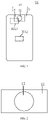
- FIG. 1 is a schematic plane view of a display substrate provided by at least one embodiment of the present disclosure.
- a display substrate 01 includes a display region 10; and the display region 10 includes a first display region 11, a second display region 12 and a third display region 13.
- the first display region 11, the second display region 12 and the third display region 13 do not overlap with each other.
- the third display region 13 at least partially surrounds (e.g., partially surrounds) the second display region 12, and the second display region 12 at least partially surrounds (e.g., completely surrounds) the first display region 11.
- the display substrate 01 may further include a peripheral region; and the peripheral region at least partially surrounds the third display region 13.
- the display substrate 01 has a first side for display and a second side opposite to the first side.
- the first side is a front side of the display substrate 01 (i.e., the plane shown in FIG. 1 ); and the second side is a back side of the display substrate.
- a sensor may be provided in the position on the second side of the display substrate 01 that corresponds to the first display region 11; and the sensor may be, for example, an image sensor or an infrared sensor, etc.
- the sensor is configured to receive light from the first side of the display substrate 01, so that operations such as image shooting, distance sensing, light intensity sensing and the like may be performed.
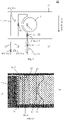
- FIG. 2 is a schematic plane view of the first display region and the second display region of the display substrate shown in FIG. 1 .
- the second display region 12 at least partially surrounds (e.g., completely surrounds) the first display region 11.
- a shape of the first display region 11 may be a circle or an ellipse; and a shape of the second display region 12 may be a rectangle, but the embodiments of the present disclosure are not limited thereto.
- the shapes of the first display region 11 and the second display region 12 may both be rectangles or other suitable shapes.
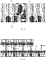
- FIG. 3 is an example of the first display region and the second display region of the display substrate shown in FIG. 2 .
- FIG. 4 is an enlarged view of a partial region REG1 of FIG. 3
- FIG. 5 is an enlarged view of a partial region REG2 of the third display region 13 of the display substrate shown in FIG. 1 .
- the first display region 11 includes at least one (e.g., a plurality of) first light-emitting elements 411.
- first light-emitting elements 411 e.g., a plurality of first light-emitting elements 411 arranged in an array; and the first light-emitting elements 411 are configured to emit light.
- the pixel circuit for driving the first light-emitting element 411 is provided in the second display region 12, so as to reduce a metal coverage area of the first display region 11 and increase light transmittance of the first display region 11.
- the pixel circuit for driving the first light-emitting element 411 will be described below, and no details will be repeated here.
- the plurality of first light-emitting elements 411 may be arranged in a plurality of light-emitting units; and these light-emitting units are arranged in an array.
- each light-emitting unit may include one or more first light-emitting elements 411.
- the plurality of first light-emitting elements 411 may emit light of a same color or may emit light of different colors, for example, may emit white light, red light, blue light, green light, etc., which may be determined according to actual needs, and is not limited in the embodiments of the present disclosure.
- the conventional arrangement mode of pixel units may be referred to, for example, GGRB, RGBG, RGB, etc., which may not be limited in the embodiments of the present disclosure.
- the first display region 11 allows light from the first side of the display substrate 01 to be at least partially transmitted to the second side of the display substrate 01.
- a sensor in the position, on the second side of the display substrate 01, corresponding to the first display region 11; and the sensor may receive light from the first side, so that operations such as image shooting, distance sensing, light intensity sensing and the like may be performed.
- the second display region 12 includes at least one (e.g., a plurality of) first pixel circuit(s) 412.
- the first light-emitting elements 411 are electrically connected with the first pixel circuits 412 in one-to-one correspondence; and the plurality of first pixel circuits 412 are used to drive the plurality of first light-emitting elements 411 in one-to-one correspondence.
- the rectangular box shown in FIG. 3 and FIG. 4 (a black-frame white-filled region indicated by reference sign 412) represents a first pixel driving unit; and each first pixel driving unit includes a first pixel circuit 412.
- the first pixel circuits 412 are configured to drive the plurality of first light-emitting elements 411 to emit light in one-to-one correspondence. That is, one first pixel circuit 412 drives one corresponding first light-emitting element 411; and different first pixel circuits 412 drive different first light-emitting elements 411.
- not all rectangular boxes represent the first pixel driving unit; when distribution density of the first pixel circuits 412 and the first light-emitting elements 411 changes (e.g., the distribution density decreases), it is possible that only some of the rectangular boxes represent the first pixel driving unit, and the other of the rectangular boxes are no longer provided therein with the first pixel driving unit.
- the first pixel driving unit may include one or more first pixel circuits 412.
- the first pixel driving unit also includes one first pixel circuit 412.
- the first pixel driving unit also includes a plurality of first pixel circuits 412.
- the amount of the first light-emitting elements 411 in each light-emitting unit is, for example, equal to the amount of the first pixel circuits 412 in each first pixel driving unit, thereby implementing driving in one-to-one correspondence.
- the plurality of first light-emitting elements 411 are arranged in an array; and the plurality of first pixel circuits 412 are also arranged in an array.
- “being arranged in an array” may refer to a plurality of devices constituting a group and a plurality of groups of devices being arranged in an array; or may also refer to the plurality of devices themselves being arranged in an array, which is not limited in the embodiments of the present disclosure.
- every 4 first light-emitting elements 411 constitute a group; and a plurality of groups of first light-emitting elements 411 are arranged in an array.
- every 4 first pixel circuits 412 constitute a group; and a plurality of groups of first pixel circuits 412 are arranged in an array.
- each first pixel driving unit includes 4 first pixel circuits 412.
- the second display region 12 further includes at least one (e.g., a plurality of) second light-emitting element(s) 421 and at least one (e.g., a plurality of) second pixel circuit(s) 422.
- the second light-emitting elements 421 are electrically connected with the second pixel circuits 422 in one-to-one correspondence; and the second pixel circuit 422 is configured to drive the second light-emitting element 421 to emit light.
- a plurality of second light-emitting elements 421 are arranged in an array; and a plurality of second pixel circuits 422 are also arranged in an array.
- at least one second light-emitting element 421 and a second pixel circuit 422 corresponding thereto constitute a second pixel driving unit 42.
- the second pixel driving unit 42 may include one second pixel circuit 422 and one second light-emitting element 421, or may include a plurality of second pixel circuits 422 and a plurality of second light-emitting elements 421.
- the amount of the second pixel circuits 422 is, for example, equal to the amount of the second light-emitting elements 421, thereby implementing driving in one-to-one correspondence.
- a plurality of second light-emitting elements 421 are arranged in an array; and a plurality of second pixel circuits 422 are also arranged in an array.
- “being arranged in an array” may refer to a plurality of devices constituting a group and a plurality of groups of devices being arranged in an array; or may also refer to a plurality of devices themselves being arranged in an array, which is not be limited in the embodiments of the present disclosure.
- every 4 second light-emitting elements 421 constitute a group; and a plurality of groups of second light-emitting elements 421 are arranged in an array.
- each second pixel driving unit 42 includes 4 second pixel circuits 422 and 4 second light-emitting elements 421.
- the third display region 13 includes at least one (e.g., a plurality of) third light-emitting element(s) 431 and at least one (e.g., a plurality of) third pixel circuit(s) 432.
- the third light-emitting elements 431 are electrically connected with the third pixel circuits 432 in one-to-one correspondence; and the third pixel circuit 432 is used to drive the third light-emitting element 431 to emit light.
- the rectangular box indicated by reference sign 432 in FIG. 5 is only used to show an approximate position of the third pixel circuit 432, and does not indicate the specific shape of the third pixel circuit 432 and the specific boundary of the third pixel circuit 432.
- a plurality of third light-emitting elements 431 are arranged in an array; and a plurality of third pixel circuits 432 are also arranged in an array.
- at least one third light-emitting element 431 and a third pixel circuit 432 corresponding thereto constitute one third pixel driving unit 43.
- the third pixel driving unit 43 may include one third pixel circuit 432 and one third light-emitting element 431, or may include a plurality of third pixel circuits 432 and a plurality of third light-emitting elements 431.
- the third pixel driving unit 43 includes a plurality of third pixel circuits 432 and a plurality of third light-emitting elements 431
- the amount of the third pixel circuits 432 is, for example, equal to the amount of the third light-emitting elements 431, thereby implementing driving in one-to-one correspondence.
- the plurality of third light-emitting elements 431 are arranged in an array; and the plurality of third pixel circuits 432 are also arranged in an array.
- “being arranged in an array” may refer to a plurality of devices constitute a group and a plurality of groups of devices being arranged in an array; or may also refer to a plurality of devices themselves being arranged in an array, which is not limited in the embodiments of the present disclosure.
- every 4 third light-emitting elements 431 constitute a group; and a plurality of groups of third light-emitting elements 431 are arranged in an array.
- each third pixel driving unit 43 includes 4 third pixel circuits 432 and 4 third light-emitting elements 431.
- PPI of the plurality of first light-emitting elements 411 in the first display region 11 is less than PPI of the plurality of second light-emitting elements 421 in the second display region 12; and PPI of the plurality of second light-emitting elements 421 in the second display region 12 is less than PPI of the plurality of third light-emitting elements 431 in the third display region 13.
- the first display region 11 and the second display region 12 may be referred to as a low-resolution region of the display substrate 01; and accordingly, the third display region 13 may be referred to as a high-resolution region of the display substrate 01.
- the sum of pixel light-emission area of the second display region 12 and pixel light-emission area of the first display region 11 may be 1/8 to 1/2 of the pixel light-emission area of the third display region 13.
- the PPI of the plurality of first light-emitting elements 411 in the first display region 11 may also be equal to the PPI of the plurality of second light-emitting elements 421 in the second display region 12, which may be determined according to actual needs, and is not limited in the embodiments of the present disclosure.
- the third display region 13 By sequentially increasing the PPI of the light-emitting elements in the first display region 11, the second display region 12, and the third display region 13, it may ensure the three display regions to emit light normally so as to display images, and at a same time, facilitate light on the first side of the display substrate 01 to pass through the first display region 11 to reach the second side, and further facilitate the sensor provided on the second side of the display substrate 01 to sense light.
- FIG. 6A is a schematic plane view I of a partial region of a display substrate provided by at least one embodiment of the present disclosure
- FIG. 6B is a schematic plane view II of a partial region of a display substrate provided by at least one embodiment of the present disclosure
- FIG. 6C is a schematic plane view III of a partial region of a display substrate provided by at least one embodiment of the present disclosure.
- the display substrate 01 is provided thereon with at least one first signal line 21, at least one second signal line 22, and at least one third signal line 23.
- the first signal line 21 includes a first main body portion 211, a first winding portion 212, a first bending portion 213, and a first connecting portion 214 that are connected in sequence.
- Both the first main body portion 211 and the first connecting portion 214 extend along a first direction; and the first direction is, for example, a column direction in which the foregoing plurality of pixel circuits or light-emitting elements are arranged in arrays.
- the embodiments of the present disclosure are not limited thereto, and the first direction may also have a certain included angle with the column direction, which may be determined according to actual needs.
- both the first main body portion 211 and the first connecting portion 214 are straight lines extending along the first direction.
- a dummy extension line of the first main body portion 211 along the first direction does not overlap with a dummy extension line of the first connecting portion 214 along the first direction, that is, the first main body portion 211 and the first connecting portion 214 are staggered from each other in a direction perpendicular to the first direction.
- the embodiments of the present disclosure are not limited thereto, and the first main body portion 211 and the first connecting portion 214 may also be a curve having a certain radian, and the curve substantially extends along the first direction.
- the first winding portion 212 extends along a curve.
- the first winding portion 212 has a distance from an edge of the first display region 11; and the first winding portion 212 extends along an extension direction of the edge of the first display region 11. That is, the first winding portion 212 does not pass through the first display region 11; and the first winding portion 212 is distributed at least partially around the first display region 11.
- a shape of the first display region 11 is a circle or an ellipse. Accordingly, the first winding portion 212 extends along an arc, and a radian of the arc is less than or equal to ⁇ .
- a separation distance between the first winding portion 212 and the edge of the first display region 11 may be set to any value, which is not limited in the embodiments of the present disclosure.
- the first bending portion 213 is, for example, composed of a plurality of folding lines for connecting the first winding portion 212 and the first connecting portion 214.
- the first winding portion 212, the first bending portion 213, and the first connecting portion 214 are all located in the second display region 12; the first main body portion 211 is at least partially located in the second display region 12; and a dummy extension line of the first main body portion 211 along the first direction passes through the first display region 11.
- none of the first main body portion 211, the first winding portion 212, the first bending portion 213, and the first connecting portion 214 is located in the first display region 11, which, thus, may avoid affecting light transmittance of the first display region 11.
- the first connecting portion 214 is electrically connected with the first pixel circuit 412.
- the first signal line 21 is configured to transmit a first driving signal to the first pixel circuit 412, so that the first pixel circuit 412 drives the first light-emitting element 411 to emit light.
- the first pixel circuit 412 is electrically connected with the first light-emitting element 411 through a connecting line 60, so that the first light-emitting element 411 may be driven to emit light.
- the connecting line 60 may be provided in a same layer as an anode of the first light-emitting element 411, and formed integrally with the anode of the first light-emitting element 411.
- an ITO layer may be separately provided to form the connecting line 60; the ITO layer is, for example, located between a source-drain metal layer (SD layer) and an anode layer of the first light-emitting element 411, and makes the connecting line 60 to be respectively electrically connected with the first pixel circuit 412 and the first light-emitting element 411 through via holes.
- SD layer source-drain metal layer
- the second signal line 22 extends along the first direction and includes a first portion 221 and a second portion 222.
- the first portion 221 is located in the third display region 13; and the second portion 222 is located in the second display region 12.
- the first portion 221 is electrically connected with the third pixel circuit 432; and the second portion 222 is electrically connected with the second pixel circuit 422.
- the second signal line 22 is configured to transmit a second driving signal to the second pixel circuit 422 and the third pixel circuit 432, so that the second pixel circuit 422 drives the second light-emitting element 421 to emit light and the third pixel circuit 432 drives the third light-emitting element 431 to emit light.
- the second signal line 22 is electrically connected with both the second pixel circuit 422 and the third pixel circuit 432, but this does not mean that the second driving signal supplied to the second pixel circuit 42 is the same as the second driving signal supplied to the third pixel circuit 432.
- progressive scanning or time-sharing scanning may be adopted, so that the second driving signal supplied to the second pixel circuit 422 is different from the second driving signal supplied to the third pixel circuit 432, so as to facilitate the corresponding second light-emitting element 421 and third light-emitting element 431 to respectively display required gray scales.
- the third signal line 23 is located in the second display region 12 and extends along the first direction; and the third signal line 23 is floating.
- the third signal line 23 is a straight line extending along the first direction.
- the third signal line 23 is a dummy line and is not electrically connected with any pixel circuit. Because the PPI of the plurality of second light-emitting elements 421 in the second display region 12 is less than the PPI of the plurality of third light-emitting elements 431 in the third display region 13, distribution density of signal lines supplying driving signals (e.g., data signals corresponding to display gray scales) in the second display region 12 is also less than distribution density thereof in the third display region 13.
- driving signals e.g., data signals corresponding to display gray scales
- the signal line supplying the driving signal (e.g., the data signal corresponding to the display gray scale) usually extends along the first direction (column direction), so, by providing the third signal line 23 extending along the first direction in the second display region 12, the difference between the distribution density of the signal lines in the second display region 12 and the distribution density of the signal lines in the third display region 13 may be effectively reduced, the circuit environment in the second display region 12 may be effectively balanced, and etching uniformity may be improved.
- the first signal line 21, the second signal line 22, and the third signal line 23 exist in the display region (e.g., the second display region 12) at the same time, and a variety of different wiring modes are provided, which, thus, may meet driving requirements of different display regions, for example, may meet the driving requirements of the first display region 11, the second display region 12, and the third display region 13 at the same time.
- the third signal line 23 and allowing the third signal line 23 to extend along the first direction the circuit environment may be effectively balanced.
- the display substrate 01 may optimize wiring design, improve rationality of layout, ensure normal display, and help improve performance of the full-screen display device.
- the display substrate 01 may also improve performance of a display device having an under-screen sensor.
- the display substrate 01 further includes at least one fourth signal line 24.
- the fourth signal line 24 is located in the third display region 13 and extends along the first direction.
- the fourth signal line 24 is a straight line extending along the first direction.
- the fourth signal line 24 is electrically connected with the third pixel circuit 432; and the fourth signal line 24 is configured to transmit a third driving signal to the third pixel circuit 432, so that the third pixel circuit 432 drives the third light-emitting element 431 to emit light.
- the third signal line 23 and the fourth signal line 24 are located on a same extension line; and there is a gap between the third signal line 23 and the fourth signal line 24, so that the third signal line 23 and the fourth signal line 24 are insulated from each other.
- the extension line is a straight line.
- the third signal line 23 and the fourth signal line 24 may be regarded as two insulated portions formed after cutting off a same signal line.
- distribution density of the third signal lines 23 in the second display region 12 may be substantially equal to distribution density of the fourth signal lines 24 in the third display region 13, so that overall signal line distribution density of the second display region 12 is not much different from overall signal line distribution density of the third display region 13, which, thus, may effectively balance the circuit environment in the display region (e.g., the second display region 12 and the third display region 13).
- the third signal line 23 and the fourth signal line 24 may be formed in a same process, thereby improving etching uniformity, simplifying the production process, improving production efficiency, and reducing production costs.
- a signal line running through the third display region 13 and the second display region 12 may be formed firstly, and then the signal line is cut off at a junction between the third display region 13 and the second display region 12, thereby forming the third signal line 23 and the fourth signal line 24, so as to be compatible with the usual panel fabrication process.
- FIG. 7 is a schematic plane view of a partial region of another display substrate provided by at least one embodiment of the present disclosure. Except for that an arrangement mode of the first signal line 21 is different, the display substrate 01 provided by this embodiment is substantially the same as the display substrate 01 shown in FIG. 6A to FIG. 6C .
- the first main body portion 211 of the first signal line 21 includes a first sub-portion 211a and a second sub-portion 211b; the first sub-portion 211a is located in the third display region 13; and the second sub-portion 211b is located in the second display region 12.
- the first sub-portion 211a is electrically connected with the third pixel circuit 432; and the second sub-portion 211b is electrically connected with the second pixel circuit 422.
- the first signal line 21 is further configured to transmit a first driving signal to the second pixel circuit 422 and the third pixel circuit 432, so that the second pixel circuit 422 drives the second light-emitting element 421 to emit light and the third pixel circuit 432 drives the third light-emitting element 431 to emit light.
- the first signal line 21 is electrically connected with the first pixel circuit 412, the second pixel circuit 422, and the third pixel circuit 432, but this does not mean that the first driving signal supplied to the first pixel circuit 412, the first driving signal supplied to the second pixel circuit 422, and the first driving signal supplied to the third pixel circuit 432 are the same.
- progressive scanning or time-sharing scanning may be used, so that the first driving signal supplied to the first pixel circuit 412, the first driving signal supplied to the second pixel circuit 422, and the first driving signal supplied to the third pixel circuit 432 are different from each other, so as to facilitate the corresponding first light-emitting element 411, the second light-emitting element 421, and the third light-emitting element 431 to respectively display required gray scales.
- the display substrate 01 includes a plurality of second pixel circuits 422 and a plurality of third pixel circuits 432.
- the plurality of second pixel circuits 422 are arranged in plurality of columns along the first direction; and the plurality of third pixel circuits 432 are arranged in plurality of columns along the first direction.
- the second pixel circuit 422 connected with the first signal line 21 and the second pixel circuit 422 connected with the second signal line 22 are located in different columns.
- the third pixel circuit 432 connected with the first signal line 21, the third pixel circuit 432 connected with the second signal line 22, and the third pixel circuit 432 connected with the fourth signal line 24 are located in different columns.
- FIG. 7 does not show the plurality of columns of pixel circuits completely, but only shows a few pixel circuits electrically connected with the first signal line 21, the second signal line 22, and the fourth signal line 24; and this does not constitute a limitation to the embodiments of the present disclosure.
- the structure shown in FIG. 3 to FIG 5 and the conventional design may be referred to, and no details will be repeated here.
- FIG. 8A is a schematic layout I of a display substrate provided by at least one embodiment of the present disclosure; and FIG. 8A is, for example, an enlarged view of a partial region REG3 in FIG. 1 .
- FIG. 8B is a schematic layout II of a display substrate provided by at least one embodiment of the present disclosure; and FIG. 8B is, for example, an enlarged view of a partial region REG4 in FIG. 8A .
- FIG. 8C is a schematic layout III of a display substrate provided by at least one embodiment of the present disclosure; and FIG. 8C is, for example, an enlarged view of a partial region REG5 in FIG. 8A .
- FIG. 8D is a schematic layout IV of a display substrate provided by at least one embodiment of the present disclosure; and FIG. 8D is, for example, another enlarged view of the partial region REG5 in FIG. 8A .
- the PPI of the plurality of first light-emitting elements 411 in the first display region 11 is substantially equal to the PPI of the plurality of second light-emitting elements 421 in the second display region 12; and the PPI of the plurality of second light-emitting elements 421 in the second display region 12 is less than the PPI of the plurality of third light-emitting elements 431 in the third display region 13.
- the first signal line 21 may supply a driving signal to the first light-emitting element 411 in the first display region 11 with lower PPI through the first pixel circuit 412; and for example, a sensor (e.g., a camera) is provided in a position corresponding to the first display region 11. Because there is no pixel circuit in the first display region 11, it is necessary to use the first signal line 21 to transmit the driving signal to the first pixel circuit 412 in the second display region 12, so that the first pixel circuit 412 drives the first light-emitting element 411 to emit light. Therefore, the first signal line 21 needs to be led in from the third display region 13 and extend around the first display region 11; and the first signal line 21 ends in position S1 in FIG. 8B .
- a sensor e.g., a camera
- the second signal line 22 may extend from the third display region 13 to the second display region 12 along the first direction (e.g., the column direction), and end in position S2 shown in FIG. 8C .
- the second signal line 22 passes through the third display region 13 and the second display region 12.
- the third signal line 23 and the fourth signal line 24 are located on a same extension line; and there is a gap between the third signal line 23 and the fourth signal line 24, so that the third signal line 23 and the fourth signal line 24 are insulated from each other. Therefore, the third signal line 23 and the fourth signal line 24 may be regarded as being disconnected from each other, for example, disconnected in position S3 in FIG. 8B .
- the third signal line 23 functions as a dummy line, so that the circuit environment in the second display region 12 may be balanced.
- the trace of the third signal line 23 is reserved, and the third signal line 23 and the fourth signal line 24 are disconnected from each other, so that uniformity of the circuit environment of the second display region 12 may be maintained.
- first bending portions 213 of different first signal lines 21 may be alternately arranged in different metal layers.
- first bending portions 213_1, 213_2, 213_3, and 213_4 respectively belong to 4 different first signal lines 21;
- the first bending portions 213_1, 213_2 may be arranged in a gate metal layer;
- the first bending portions 213_3, 213_4 may be arranged in a first metal layer, which, thus, may facilitate wiring and avoid short circuits at overlapping lines.
- the first metal layer may be any film layer different from the gate metal layer in the display substrate 01, which is not limited in the embodiments of the present disclosure.
- FIG. 9 is a schematic plane view of a partial region of a display substrate provided by at least one embodiment of the present disclosure.
- the display substrate 01 includes a plurality of first signal lines 21, a plurality of second signal lines 22, and a plurality of third signal lines 23.
- the plurality of second signal lines 22 and the plurality of third signal lines 23 are arranged at intervals, so as to more effectively balance the circuit environment of the second display region 12.
- the plurality of second signal lines 22 and the first connecting portions 214 of the plurality of first signal lines 21 are arranged at intervals, which, thus, may effectively utilize wiring space of the second display region 12, optimize wiring design, and improve rationality of layout.
- Other structures of the display substrate 01 are substantially the same as the display substrate 01 provided by the foregoing embodiments, and no details will be repeated here.
- the second signal lines 22 and the third signal lines 23 may be arranged at intervals according to a quantity ratio of 1:1, or may also be arranged at intervals according to any quantity ratio such as 2:1, 3:1, etc.
- the second signal lines 22 and the first connecting portions 214 may be arranged at intervals according to a quantity ratio of 1:1, or may also be arranged at intervals according to any quantity ratio such as 2:1, 3:1, etc., which may be determined according to actual needs, and is not limited in the embodiments of the present disclosure.
- the respective amounts of the first signal lines 21, the second signal lines 22, and the third signal lines 23 are not limited, and may be determined according to actual needs, for example, according to factors such as the size of the display substrate 01, PPI, etc., which is not limited in the embodiments of the present disclosure.
- the driving signals transmitted by the first signal line 21, the second signal line 22, and the fourth signal line 24 are data signals, that is, the first signal line 21, the second signal line 22, and the fourth signal line 24 may be data lines; and the first driving signal, the second driving signal, and the third driving signal are all data signals.
- the data signals correspond to display gray scales.
- the first driving signal, the second driving signal, and the third driving signal may be different data signals or a same data signal, which is not limited in the embodiments of the present disclosure.
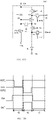
- FIG. 10A is a schematic structural diagram of a 7T1C pixel circuit.
- the foregoing first pixel circuit 412, the foregoing second pixel circuit 422, and the foregoing third pixel circuit 432 may all adopt the 7T1C pixel circuit.
- the 7T1C pixel circuit 100 includes a first transistor CT1, a second transistor CT2, a third transistor CT3, a fourth transistor CT4, a fifth transistor CT5, a sixth transistor CT6, a seventh transistor CT7, and a storage capacitor Cst.
- the first transistor CT1 to the seventh transistor CT7 are all P-type transistors.
- a first terminal of the storage capacitor Cst is connected with a first power supply voltage terminal VDD to receive a first power supply voltage VI; and a second terminal of the storage capacitor Cst is connected with a first node N1.
- a first terminal of a light-emitting element EL is connected with a fourth node N4; and a second terminal of the light-emitting element EL is connected with a second power supply voltage terminal VSS to receive a second power supply voltage V2.
- a control terminal of the first transistor CT1 is connected with the first node N1; a first terminal of the first transistor CT1 is connected with a second node N2; and a second terminal of the first transistor CT1 is connected with a third node N3.
- a first terminal of the second transistor CT2 is connected with the second node N2; and a second terminal of the second transistor CT2 is connected with a data signal terminal DAT to receive a data signal (e.g., a data voltage) Vdata.
- a first terminal of the third transistor CT3 is connected with the first node N1; and a second terminal of the third transistor CT3 is connected with the third node N3.
- a first terminal of the fourth transistor CT4 is connected with the first node N1; and a second terminal of the fourth transistor CT4 is connected with a first reset signal terminal Init1 to receive a first reset signal Vinit1 supplied by the first reset signal terminal Init1.
- a first terminal of the fifth transistor CT5 is connected with the first power supply voltage terminal VDD; and the second terminal of the fifth transistor CT5 is connected with the second node N2.
- a first terminal of the sixth transistor CT6 is connected with the fourth node N4; and a second terminal of the sixth transistor CT6 is connected with a second reset signal terminal Init2 to receive a second reset signal Vinit2.
- a first terminal of the seventh transistor CT7 is connected with the third node N3; and a second terminal of the seventh transistor CT7 is connected with the fourth node N4.
- a control terminal GAT1 of the second transistor CT2 and a control terminal GAT2 of the third transistor CT3 are both coupled to a scan signal terminal GAT (not shown in the figure);
- a control terminal EM1 of the fifth transistor CT5 and a control terminal EM2 of the seventh transistor CT7 are both coupled to a light emission control terminal EM (not shown in the figure);
- a control terminal of the fourth transistor CT4 is connected with a first reset control terminal RST1; and a control terminal of the sixth transistor CT6 is connected with a second reset control terminal RST2.
- FIG. 10A also shows the first node N1, the second node N2, the third node N3, the fourth node N4, and the light-emitting element EL.
- FIG. 10B is a driving timing diagram of the 7T1C pixel circuit shown in FIG. 10A .
- each driving cycle of the 7T1C pixel circuit 100 includes a first phase t1, a second phase t2, and a third phase t3.
- the first reset control terminal RST1 receives an active level; and the scan signal terminal GAT, the second reset control terminal RST2 and the light emission control terminal EM all receive an inactive level.
- the fourth transistor CT4 is turned on, the second transistor CT2, the third transistor CT3, the fifth transistor CT5, the sixth transistor CT6, and the seventh transistor CT7 are turned off; the fourth transistor CT4 is configured to receive the first reset signal (e.g., a reset voltage) Vinit1, and write the first reset signal Vinit1 to the storage capacitor Cst to reset the storage capacitor Cst; a voltage of the first node N1 is Vinit1, and Vinit1 is, for example, a negative value.
- the first transistor CT1 is turned on.
- the scan signal terminal GAT and the second reset control terminal RST2 receive an active level
- the first reset control terminal RST1 and the light emission control terminal EM receive an inactive level
- the first transistor CT1 to the third transistor CT3 and the sixth transistor CT6 are turned on, the fourth transistor CT4, the fifth transistor CT5 and the seventh transistor CT7 are turned off;
- the second transistor CT2 receives the data signal Vdata, and the data signal Vdata is written by the turned-on first transistor CT1 and the turned-on third transistor CT3 to the control terminal of the first transistor CT1,
- the storage capacitor Cst stores the data signal Vdata written to the control terminal of the first transistor CT1 at the control terminal of the first transistor CT1, a voltage of the first node N1 is Vdata+Vth;
- the sixth transistor CT6 is configured to receive a second reset signal (e.g., a reset voltage) Vinit2, and write the second reset signal Vinit2 to the first terminal of the light-emitting element EL, so as to reset the first terminal of the light-emitting element EL.
- a voltage of the fourth node N4 is Vinit2, and Vinit2 is, for example, a negative value.
- the light emission control terminal EM receives an active level
- the first reset control terminal RST1 receives an active level
- the scan signal terminal GAT receives an inactive level
- the first transistor CT1, the fifth transistor CT5, and the seventh transistor CT7 are turned on, the second transistor CT2, the third transistor CT3, the fourth transistor CT4, and the sixth transistor CT6 are turned off;
- the first transistor CT1 is configured to control a driving current that flows through the first transistor CT1 and from the first power supply voltage terminal VDD to the light-emitting element EL and is used to drive the light-emitting element EL, based on the data signal (e.g., data voltage) Vdata stored in the storage capacitor Cst and the received first power supply voltage VI;
- a voltage of the first node N1 is Vdata+Vth, a voltage of the second node N2 is VDD;
- k ⁇ Cox ⁇ W/L; ⁇ is mobility of carriers in the first transistor CT1, Cox is capacitance of a gate oxide layer of the first transistor CT1, W/L is a width-to-length ratio of a channel of the first transistor CT1, Vth is a threshold voltage of the first transistor CT1, Vth is a gate-source voltage of the first transistor CT1, Vg is a gate voltage of the first transistor CT1, and Vs is a source voltage of the first transistor CT1.
- the driving current Id generated by the first transistor CT1 is irrelevant to the threshold voltage of the first transistor CT1, so the 7T1C pixel circuit 100 shown in FIG. 10A and FIG. 10B has a threshold compensation function.
- the first pixel circuit 412, the second pixel circuit 422, and the third pixel circuit 432 are not limited to adopting the above-described 7T1C pixel circuit, and other applicable pixel circuits may also be used, which is not limited in the embodiments of the present disclosure.
- Specific circuit structures of the first pixel circuit 412, the second pixel circuit 422, and the third pixel circuit 432 may be the same or different from each other, which may be determined according to actual needs, and is not limited in the embodiments of the present disclosure.
- each of the first pixel circuit 412, the second pixel circuit 422, and the third pixel circuit 432 includes a switching thin film transistor; and the switching thin film transistor is, for example, the second transistor CT2 in FIG. 10A .
- the switching thin film transistor e.g., the second transistor CT2
- the switching thin film transistor includes a gate electrode, a first electrode and a second electrode; the first signal line 21, the second signal line 22 or the fourth signal line 24 is electrically connected with the first electrode or the second electrode of the switching thin film transistor. That is, the first signal line 21, the second signal line 22, or the fourth signal line 24 may be electrically connected with the data signal terminal DAT in FIG. 10A to supply the data signal.
- the foregoing first light-emitting element 411, the foregoing second light-emitting element 421, and the foregoing third light-emitting element 431 include an organic light-emitting diode (OLED). That is, the first light-emitting element 411, the second light-emitting element 421, or the third light-emitting element 431 may be the light-emitting element EL in FIG. 10A ; and the light-emitting element EL may be an OLED.
- OLED organic light-emitting diode
- the embodiments of the present disclosure are not limited thereto; and the first light-emitting element 411, the second light-emitting element 421, and the third light-emitting element 431 may also be quantum dot light-emitting diodes (QLEDs) or other applicable light-emitting devices, which may not be limited in the embodiments of the present disclosure.
- QLEDs quantum dot light-emitting diodes
- FIG. 11 is a schematic diagram of a laminated structure of a display substrate provided by at least one embodiment of the present disclosure; and the schematic diagram of the laminated structure mainly schematically shows the first pixel circuit 412 and the first light-emitting element 411.
- the first pixel circuit 412 includes structures such as a switching thin film transistor 412T and a storage capacitor 412C.
- the first light-emitting element 411 includes a first anode structure 4111, a first cathode structure 4113, and a first light emitting layer 4112 located between the first anode structure 4111 and the first cathode structure 4113; and the first anode structure 4111 is electrically connected with the switching thin film transistor 412T included in the first pixel circuit 412 through a via hole.
- the first anode structure 4111 may be integrally formed with the foregoing connecting line 60, that is, the connecting line 60 may be regarded as a portion of the first anode structure 4111.
- an ITO layer may be separately provided to form the connecting line 60; and the ITO layer is, for example, located between the source-drain metal layer (SD layer) and a film layer where the first anode structure 4111 is located, and implements required electrical connection through a via hole.
- the first anode structure 4111 may include a plurality of anode sub-layers, for example, may include an ITO/Ag/ITO three-layer structure (not shown in the figure), etc.; and the specific form of the first anode structure 4111 is not limited in the embodiments of the present disclosure.
- the first cathode structure 4113 may be a structure formed on an entire surface of the display substrate 01; and the first cathode structure 4113, for example, may include metal materials such as lithium (Li), aluminum (Al), magnesium (Mg), silver (Ag), etc.
- the first cathode structure 4113 may be formed as a very thin layer, the first cathode structure 4113 has good light transmittance.
- the switching thin film transistor 412T includes an active layer 4121, a gate electrode 4122, and a source-drain electrode (i.e., a source electrode 4123 and a drain electrode 4124); and the storage capacitor 412C includes a first capacitor plate 4125 and a second capacitor plate 4126.
- the active layer 4121 is provided on a base substrate 74; and a first gate insulating layer 741 is provided on a side of the active layer 4121 away from the base substrate 74.
- the gate electrode 4122 is provided in a same layer as the first capacitor plate 4125 and is located on a side of the first gate insulating layer 741 away from the base substrate 74; and a second gate insulating layer 742 is provided on a side of the gate electrode 4122 and the first capacitor plate 4125 away from the base substrate 74.
- the second capacitor plate 4126 is provided on a side of the second gate insulating layer 742 away from the base substrate 74, and an interlayer insulating layer 743 is provided on a side of the second capacitor plate 4126 away from the base substrate 74.
- the source-drain electrode is provided on a side of the interlayer insulating layer 743 away from the base substrate 74, and is electrically connected with the active layer 4121 through via holes located in the first gate insulating layer 741, the second gate insulating layer 742, and the interlayer insulating layer 743.
- a planarization layer 744 is provided on a side of the source-drain electrode away from the base substrate 74 to planarize the first pixel circuit 412.
- the planarization layer 744 has a via hole; and the first anode structure 4111 is electrically connected with the source electrode 4123 or the drain electrode 4124 of the switching thin film transistor 412T through the via hole in the planarization layer 744.
- the first display region 11 further includes a transparent support layer 78 located on the base substrate 74; and the first light-emitting element 411 is located on a side of the transparent support layer 78 away from the base substrate 74.
- the first light-emitting element 411 in the first display region 11 may be located at a height substantially the same as the second light-emitting element 421 in the second display region 12 and the third light-emitting element 431 in the third display region 13, so that the display effect of the display substrate 01 may be improved.
- the first main body portion 211, the first winding portion 212, the first connecting portion 214, the second signal line 22, and the third signal line 23 may be located in a same layer.
- the film layer where the source-drain electrode i.e., the source electrode 4123 and the drain electrode 4124
- SD layer source-drain metal layer
- the first main body portion 211, the first winding portion 212, the first connecting portion 214, the second signal line 22, and the third signal line 23 are located in the source-drain metal layer, that is, arranged in a same layer as the source electrode 4123 and the drain electrode 4124.
- the first bending portion 213 and the first connecting portion 214 are located in different layers; and in the case where the first main body portion 211, the first winding portion 212, the first connecting portion 214, the second signal line 22 and the third signal line 23 are arranged in a same layer, the first bending portion 213 is located in a layer different from any one of the first main body portion 211, the first winding portion 212, the first connecting portion 214, the second signal line 22, and the third signal line 23.
- the film layer where the gate electrode 4122 is located is referred to as a gate metal layer, that is, as shown in FIG.
- the gate electrode 4122 of the switching thin film transistor 412T is located in the gate metal layer.
- the first bending portion 213 of at least one of the first signal lines 21 is located in the gate metal layer, that is, the first bending portion 213 of at least one of the first signal lines 21 is provided in a same layer as the gate electrode 4122.
- the display substrate 01 may further include a first metal layer; the first metal layer and the gate metal layer are different film layers; and the first metal layer is insulated from the gate metal layer.
- the first metal layer is any other metal layer different from the gate metal layer in the display substrate 01.
- first bending portions 213 of some first signal lines 21 are located in the gate metal layer, and first bending portions 213 of the other first signal lines 21 are located in the first metal layer.
- first bending portions 213 of different first signal lines 21 may be alternately arranged in the gate metal layer and the first metal layer. For example, as shown in FIG.
- first bending portions 213 of different first signal lines 21 may be alternately arranged in a same layer as the gate electrode 4122 and the second capacitor plate 4126, that is, first bending portions 213 of some first signal lines 21 are arranged in a same layer as the gate electrode 4122, and first bending portions 213 of the other first signal lines 21 are arranged in a same layer as the second capacitor plate 4126.
- the above-described arrangement mode can be compatible with the existing process, make minor changes to the process, facilitate wiring, and may reduce difficulties in wiring design.
- the embodiments of the present disclosure are not limited thereto; in some other examples, the first signal line 21, the second signal line 22, and the third signal line 23 may also be located in a same layer, that is, located in a same film layer in the display substrate 01, which, thus, may reduce the thickness of the display substrate 01, facilitate preparation in a same process, and simplify the preparation process.
- the film layer relationship of the first signal line 21, the second signal line 22, and the third signal line 23 may be determined according to actual needs, and the three may be located in a same layer or different layers, which is not limited in the embodiments of the present disclosure.
- any two of the first signal line 21, the second signal line 22, and the third signal line 23 may be located in a same layer, and the rest may be located in a different layer; or, all the three may be located in different layers.
- the fourth signal line 24 may be located in a same layer as any one or more of the first signal line 21, the second signal line 22, and the third signal line 23, or may be located in a layer different from the first signal line 21, the second signal line 22 and the third signal line 23, which is not limited in the embodiments of the present disclosure.
- the first signal line 21, the second signal line 22, and the third signal line 23 include a metal trace; and at least a portion of the metal trace, for example, is located in the source-drain metal layer of the display substrate 01.
- a portion of the metal trace except for the first bending portion 213 is entirely located in the source-drain metal layer. Therefore, when preparing the source electrode and the drain electrode in the source-drain metal layer, the second signal line 22, the third signal line 23, as well as the first main body portion 211, the first winding portion 212 and the first connecting portion 214 of the first signal line 21 may be prepared together, which, thus, may simplify the production process, improve production efficiency, and reduce production costs. In this case, when preparing the gate electrode in the gate metal layer, the metal trace serving as the first bending portion 213 may be prepared together.
- the first signal line 21, the second signal line 22, and the third signal line 23 may include a transparent conductive trace, which is made of, for example, indium tin oxide (ITO).
- the transparent conductive trace may be provided in any suitable film layer, which is not limited in the embodiments of the present disclosure.
- the display substrate 01 further includes structures such as a pixel defining layer 746, an encapsulation layer 747, etc.
- the pixel defining layer 746 is provided on the first anode structure 4111 (e.g., a portion of the first anode structure 4111), and includes a plurality of openings to define different pixels or sub-pixels; and the first light emitting layer 4112 is formed in the openings of the pixel defining layer 746.
- the encapsulation layer 747 may include a single-layer or multi-layer encapsulation structure, for example, the multi-layer encapsulation structure includes a laminate of an inorganic encapsulation layer and an organic encapsulation layer, thereby improving the encapsulation effect on the display substrate 01.
- the pixel defining layers 746 in the first display region 11, the second display region 12, and the third display region 13 are arranged in a same layer; and the encapsulation layers 747 in the first display region 11, the second display region 12 and the third display region 13 are arranged in a same layer, or may also be integrally connected in some embodiments, which is not limited in the embodiments of the present disclosure.
- the base substrate 74 may be a glass substrate, a quartz substrate, a metal substrate, or a resin substrate, etc., and may be a rigid substrate or a flexible substrate, which is not limited in the embodiments of the present disclosure.
- the first gate insulating layer 741, the second gate insulating layer 742, the interlayer insulating layer 743 as well as the planarization layer 744, the insulating layer 745, the pixel defining layer 746, and the encapsulation layer 747 may include inorganic insulating materials such as silicon oxide, silicon nitride, silicon oxynitride, or may include organic insulating materials such as polyimide, polyphthalimide, polyamide, acrylic resin, benzocyclobutene, or phenolic resin. Materials of the above-described respective functional layers are not specifically limited in the embodiments of the present disclosure.
- a material of the active layer 4121 may include semiconductor materials such as polysilicon or oxide semiconductor (e.g., indium gallium zinc oxide).
- semiconductor materials such as polysilicon or oxide semiconductor (e.g., indium gallium zinc oxide).
- a portion of the active layer 4121 may be conductorized by a conductorization process such as doping, so as to have higher conductivity.
- materials of the gate electrode 4122, the first capacitor plate 4125, and the second capacitor plate 4126 may include metal materials or alloy materials, for example, include molybdenum, aluminum, and titanium, etc.
- materials of the source electrode 4123 and the drain electrode 4124 may include metal materials or alloy materials, for example, a metal single-layer or multi-layer structure formed of molybdenum, aluminum, titanium, etc.
- the multi-layer structure is a multi-metal laminated layer, for example, titanium, aluminum, titanium (Ti/Al/Ti) metal laminated layer, etc.
- the display substrate 01 provided by the embodiments of the present disclosure may be an organic light-emitting diode (OLED) display substrate or a quantum dot light-emitting diode (QLED) display substrate, etc.; and the specific type of the display substrate is not limited in the embodiments of the present disclosure.
- OLED organic light-emitting diode
- QLED quantum dot light-emitting diode
- the light emitting layer may include small molecular organic materials or polymer molecular organic materials, which may be fluorescent light-emitting materials or phosphorescent light-emitting materials, and may emit red light, green light, blue light, or white light.
- the light emitting layer may further include functional layers such as an electron injection layer, an electron transport layer, a hole injection layer, and a hole transport layer according to different actual needs.
- the light emitting layer may include quantum dot materials, for example, silicon quantum dots, germanium quantum dots, cadmium sulfide quantum dots, cadmium selenide quantum dots, cadmium telluride quantum dots, zinc selenide quantum dots, lead sulfide quantum dots, lead selenide quantum dots, indium phosphide quantum dots and indium arsenide quantum dots, etc. and a particle size of a quantum dot ranges, for example, from 2 nm to 20 nm.
- quantum dot materials for example, silicon quantum dots, germanium quantum dots, cadmium sulfide quantum dots, cadmium selenide quantum dots, cadmium telluride quantum dots, zinc selenide quantum dots, lead sulfide quantum dots, lead selenide quantum dots, indium phosphide quantum dots and indium arsenide quantum dots, etc.
- a particle size of a quantum dot ranges, for example, from 2 nm to 20 nm.
- At least one embodiment of the present disclosure further provides a display device; and the display device includes the display substrate provided by any one embodiment of the present disclosure.
- the display device can meet driving requirements of different display regions, and can balance the circuit environment, optimize wiring design, improve rationality of layout, ensure normal display, and help improve performance of a full-screen display device.
- FIG. 12 is a schematic block diagram of a display device provided by at least one embodiment of the present disclosure.
- a display device 30 includes a display substrate 310; and the display substrate 310 is the display substrate provided by any one embodiment of the present disclosure, for example, the foregoing display substrate 01.
- the display device 30 may be any electronic device having a display function, for example, a smart phone, a laptop, a tablet personal computer, a television, etc.
- the smart phone or the tablet personal computer may have full-screen design, that is, there is no peripheral region surrounding the third display region 13.
- the smart phone or the tablet personal computer also has an under-screen sensor (e.g., a camera, an infrared sensor, etc.), which may perform operations such as image shooting, distance sensing, light intensity sensing, etc.
- an under-screen sensor e.g., a camera, an infrared sensor, etc.
- FIG. 13 is a schematic diagram of a laminated structure of a display device provided by at least one embodiment of the present disclosure.
- the display device 30 includes a display substrate 310; and the display substrate 310 is the display substrate provided by any one embodiment of the present disclosure, for example, the foregoing display substrate 01.
- the display device 30 further includes a sensor 320.
- the display substrate 01 includes a first side F1 for display and a second side F2 opposite to the first side F1. That is, the first side F1 is a display side, and the second side F2 is a non-display side.
- the display substrate 01 is configured to perform a display operation on the first side F1, that is, the first side F1 of the display substrate 01 is a light emergent side of the display substrate 01, and the first side F1 faces the user.
- the first side F1 and the second side F2 are opposed to each other in a normal line direction of a display surface of the display substrate 01.
- the sensor 320 is provided on the second side F2 of the display substrate 01; and the sensor 320 is configured to receive light from the first side F1.
- the sensor 320 and the first display region 11 are stacked in the normal line direction of the display surface of the display substrate 01 (e.g., a direction perpendicular to the display substrate 01); the sensor 320 may receive and process a light signal passing through the first display region 11; and the light signal may be visible light, infrared light, etc.
- the first display region 11 allows light from the first side F1 to be at least partially transmitted to the second side F2.
- the first display region 11 is not provided with a pixel circuit, and in this case, light transmittance of the first display region 11 can be improved.
- an orthogonal projection of the sensor 320 on the display substrate 01 at least partially overlaps with the first display region 11.
- the orthogonal projection of the sensor 320 on the display substrate 01 is located within the first display region 11.
- the orthogonal projection of the sensor 320 on the display substrate 01 partially overlaps with the first display region 11. In this case, because light can propagate laterally to the sensor 320, the sensor 320 does not need to be completely located in a position corresponding to the first display region 11.
- the first display region 11 may be referred to as a high light-transmittance region of a low-resolution region of the display substrate 01.
- the senor 320 may be an image sensor, which may be used to acquire an image of an external environment facing a light-collecting surface of the sensor 320, and may be, for example, a complementary metal oxide semiconductor (CMOS) image sensor or a charge coupled device (CCD) image sensor.
- CMOS complementary metal oxide semiconductor
- CCD charge coupled device
- the sensor 320 may also be an infrared sensor, a distance sensor, or the like.
- the sensor 320 may be implemented as a camera of a mobile terminal such as a mobile phone, a laptop, etc., and may also include, for example, an optical device such as a lens, a mirror, or an optical waveguide according to needs, so as to modulate the optical path.
- the sensor 320 may include photosensitive pixels arranged in an array.
- each photosensitive pixel may include a photosensitive detector (e.g., a photodiode, a phototransistor) and a switch transistor (e.g., a switching thin film transistor).
- the photodiode may convert a light signal irradiated thereon into an electrical signal; and the switch transistor may be electrically connected with the photodiode to control whether the photodiode is in a state of collecting a light signal and the time for collecting the light signal.
- the anode of the first light-emitting element 411 adopts a ITO/Ag/ITO laminated structure, then in the first display region 11, only the anode of the first light-emitting element 411 is opaque, that is, a trace used for driving the first light-emitting element 411 bypasses the first display region 11 or is set as a transparent trace. In this case, not only can light transmittance of the first display region 11 be further improved, but also diffraction caused by various elements in the first display region 11 may be reduced.
- the display device 30 may further include more components and structures, which are not limited in the embodiments of the present disclosure.
- the above description about the display substrate 01 may be referred to, and no details will be repeated here.
Abstract
Description
- The present application claims priority of
Chinese Patent Application No. 202010479767.2, filed on May 29, 2020 - Embodiments of the present disclosure relate to a display substrate and a display device.
- Organic light-emitting diode (OLED) display devices have characteristics such as wide viewing angle, high contrast, fast response speed, wide color gamut, high screen-to-body ratio, self-luminescence, lightness and thinness, and the like. Due to the above-described characteristics and advantages, the OLED display devices gradually receive widespread attention and can be applied to devices having a display function, such as mobile phones, monitors, laptops, smart watches, digital cameras, instruments and meters, flexible wearable devices, etc. With further development of the display technology, display devices having a high screen-to-body ratio can no longer meet people' needs, and display devices having a full screen have become a development trend of the future display technology.
- At least one embodiment of the present disclosure provides a display substrate, and the display substrate has a first side for display and a second side opposite to the first side, and comprises a display region. The display region comprises a first display region, a second display region, and a third display region, the second display region at least partially surrounds the first display region, the third display region at least partially surrounds the second display region, and the first display region, the second display region, and the third display region do not overlap with each other; the first display region comprises at least one first light-emitting element, and the first display region allows light from the first side to be at least partially transmitted to the second side; the second display region comprises at least one first pixel circuit, at least one second light-emitting element, and at least one second pixel circuit, the first light-emitting element is electrically connected with the first pixel circuit, and the second light-emitting element is electrically connected with the second pixel circuit; the third display region comprises at least one third light-emitting element and at least one third pixel circuit, and the third light-emitting element is electrically connected with the third pixel circuit; the display substrate is provided with at least one first signal line, at least one second signal line, and at least one third signal line; the first signal line comprises a first main body portion, a first winding portion, a first bending portion, and a first connecting portion that are connected in sequence; the first main body portion and the first connecting portion both extend along a first direction, a dummy extension line of the first main body portion along the first direction does not overlap with a dummy extension line of the first connecting portion along the first direction, and the first winding portion extends along a curve; the first winding portion, the first bending portion, and the first connecting portion are all in the second display region, the first main body portion is at least partially in the second display region, and the dummy extension line of the first main body portion along the first direction passes through the first display region; the first connecting portion is electrically connected with the first pixel circuit, the first signal line is configured to transmit a first driving signal to the first pixel circuit, so that the first pixel circuit drives the first light-emitting element to emit light; the second signal line extends along the first direction and comprises a first portion and a second portion, the first portion is in the third display region, and the second portion is in the second display region; the first portion is electrically connected with the third pixel circuit, the second portion is electrically connected with the second pixel circuit, the second signal line is configured to transmit a second driving signal to the second pixel circuit and the third pixel circuit, so that the second pixel circuit drives the second light-emitting element to emit light and the third pixel circuit drives the third light-emitting element to emit light; and the third signal line is in the second display region and extends along the first direction, and the third signal line is floating.
- For example, the display substrate provided by an embodiment of the present disclosure further comprises at least one fourth signal line. The fourth signal line is in the third display region and extends along the first direction, the fourth signal line is electrically connected with the third pixel circuit, and the fourth signal line is configured to transmit a third driving signal to the third pixel circuit, so that the third pixel circuit drives the third light-emitting element to emit light; and the third signal line and the fourth signal line are located on a same extension line, and there is a gap between the third signal line and the fourth signal line, so that the third signal line and the fourth signal line are insulated from each other.
- For example, in the display substrate provided by an embodiment of the present disclosure, the extension line is a straight line.
- For example, in the display substrate provided by an embodiment of the present disclosure, the first main body portion of the first signal line comprises a first sub-portion and a second sub-portion, the first sub-portion is in the third display region, and the second sub-portion is in the second display region; the first sub-portion is electrically connected with the third pixel circuit, and the second sub-portion is electrically connected with the second pixel circuit; and the first signal line is further configured to transmit the first driving signal to the second pixel circuit and the third pixel circuit, so that the second pixel circuit drives the second light-emitting element to emit light and the third pixel circuit drives the third light-emitting element to emit light.
- For example, in the display substrate provided by an embodiment of the present disclosure, the at least one second pixel circuit comprises a plurality of second pixel circuits, and the plurality of second pixel circuits are arranged in a plurality of columns along the first direction; and second pixel circuits connected with the first signal line and second pixel circuits connected with the second signal line are located in different columns.
- For example, in the display substrate provided by an embodiment of the present disclosure, the at least one third pixel circuit comprises a plurality of third pixel circuits, and the plurality of third pixel circuits are arranged in a plurality of columns along the first direction; and third pixel circuits connected with the first signal line, third pixel circuits connected with the second signal line, and third pixel circuits connected with the fourth signal line are located in different columns.
- For example, in the display substrate provided by an embodiment of the present disclosure, the first winding portion has a distance from an edge of the first display region, and the first winding portion extends along an extension direction of the edge of the first display region.
- For example, in the display substrate provided by an embodiment of the present disclosure, a shape of the first display region is a circle or an ellipse, and the first winding portion extends along an arc.
- For example, in the display substrate provided by an embodiment of the present disclosure, the at least one second signal line comprises a plurality of second signal lines, the at least one third signal line comprises a plurality of third signal lines, and the plurality of second signal lines and the plurality of third signal lines are arranged at intervals.
- For example, in the display substrate provided by an embodiment of the present disclosure, the at least one second signal line comprises a plurality of second signal lines, the at least one first signal line comprises a plurality of first signal lines, and the plurality of second signal lines and first connecting portions of the plurality of first signal lines are arranged at intervals.
- For example, in the display substrate provided by an embodiment of the present disclosure, the first driving signal, the second driving signal, and the third driving signal are different data signals or same data signals, and the data signals correspond to display gray scales.
- For example, in the display substrate provided by an embodiment of the present disclosure, each of the first pixel circuit, the second pixel circuit, and the third pixel circuit comprises a switching thin film transistor, and the switching thin film transistor comprises a gate electrode, a first electrode and a second electrode; and the first signal line, the second signal line, or the fourth signal line is electrically connected with the first electrode or the second electrode of the switching thin film transistor.
- For example, in the display substrate provided by an embodiment of the present disclosure, the first main body portion, the first winding portion, the first connecting portion, the second signal line, and the third signal line are in a same layer.
- For example, the display substrate provided by an embodiment of the present disclosure further comprises a source-drain metal layer. The first electrode and the second electrode of the switching thin film transistor are in the source-drain metal layer, and the first main body portion, the first winding portion, the first connecting portion, the second signal line, and the third signal line are in the source-drain metal layer.
- For example, in the display substrate provided by an embodiment of the present disclosure, the first bending portion and the first connecting portion are in different layers.
- For example, the display substrate provided by an embodiment of the present disclosure further comprises a gate metal layer. The gate electrode of the switching thin film transistor is in the gate metal layer, and the first bending portion of at least one of the first signal lines is in the gate metal layer.
- For example, the display substrate provided by an embodiment of the present disclosure further comprises a first metal layer. The first metal layer is a film layer different from the gate metal layer, and is insulated from the gate metal layer, the at least one first signal line comprises a plurality of first signal lines, first bending portions of part of the first signal lines are in the gate metal layer, and first bending portions of other part of the first signal lines are in the first metal layer.
- For example, in the display substrate provided by an embodiment of the present disclosure, the first signal line, the second signal line, and the third signal line comprise a metal trace or a transparent conductive trace.
- For example, in the display substrate provided by an embodiment of the present disclosure, the first light-emitting element, the second light-emitting element, and the third light-emitting element comprise an organic light-emitting diode.
- For example, in the display substrate provided by an embodiment of the present disclosure, pixels per inch of second light-emitting elements in the second display region is less than pixels per inch of third light-emitting elements in the third display region.
- At least one embodiment of the present disclosure further provides a display device, which comprises the display substrate provided by any one of the embodiments of the present disclosure.
- For example, the display device provided by an embodiment of the present disclosure further comprises a sensor. The sensor is provided on the second side of the display substrate, and the sensor is configured to receive the light from the first side.
- For example, in the display device provided by an embodiment of the present disclosure, an orthogonal projection of the sensor on the display substrate at least partially overlaps with the first display region.
- In order to clearly illustrate the technical solution of the embodiments of the present disclosure, the drawings of the embodiments will be briefly described in the following. It is obvious that the described drawings in the following are only related to some embodiments of the present disclosure and thus are not limitative of the present disclosure.
-
FIG. 1 is a schematic plane view of a display substrate provided by at least one embodiment of the present disclosure; -
FIG. 2 is a schematic plane view of a first display region and a second display region of the display substrate shown inFIG.1 ; -
FIG. 3 is an example of the first display region and the second display region of the display substrate shown inFIG.2 ; -
FIG. 4 is an enlarged view of a partial region ofFIG.3 ; -
FIG. 5 is an enlarged view of a partial region of a third display region of the display substrate shown inFIG.1 ; -
FIG. 6A is a schematic plane view I of a partial region of a display substrate provided by at least one embodiment of the present disclosure; -
FIG. 6B is a schematic plane view II of a partial region of a display substrate provided by at least one embodiment of the present disclosure; -
FIG. 6C is a schematic plane view III of a partial region of a display substrate provided by at least one embodiment of the present disclosure; -
FIG. 7 is a schematic plane view of a partial region of another display substrate provided by at least one embodiment of the present disclosure; -
FIG. 8A is a schematic layout I of a display substrate provided by at least one embodiment of the present disclosure; -
FIG. 8B is a schematic layout II of a display substrate provided by at least one embodiment of the present disclosure; -
FIG. 8C is a schematic layout III of a display substrate provided by at least one embodiment of the present disclosure; -
FIG. 8D is a schematic layout IV of a display substrate provided by at least one embodiment of the present disclosure; -
FIG. 9 is a schematic plane view of a partial region of a display substrate provided by at least one embodiment of the present disclosure; -
FIG. 10A is a schematic structural diagram of a 7T1C pixel circuit; -
FIG. 10B is a driving timing diagram of the 7T1C pixel circuit shown inFIG. 10A ; -
FIG. 11 is a schematic diagram of a laminated structure of a display substrate provided by at least one embodiment of the present disclosure; -
FIG. 12 is a schematic block diagram of a display device provided by at least one embodiment of the present disclosure; and -
FIG. 13 is a schematic diagram of a laminated structure of a display device provided by at least one embodiment of the present disclosure. - In order to make objects, technical details and advantages of the embodiments of the disclosure apparent, the technical solutions of the embodiments will be described in a clearly and fully understandable way in connection with the drawings related to the embodiments of the disclosure. Apparently, the described embodiments are just a part but not all of the embodiments of the disclosure. Based on the described embodiments herein, those skilled in the art can obtain other embodiment(s), without any inventive work, which should be within the scope of the disclosure.
- Unless otherwise defined, all the technical and scientific terms used herein have the same meanings as commonly understood by one of ordinary skill in the art to which the present disclosure belongs. The terms "first," "second," etc., which are used in the description and the claims of the present application for disclosure, are not intended to indicate any sequence, amount or importance, but distinguish various components. Also, the terms such as "a," "an," etc., are not intended to limit the amount, but indicate the existence of at least one. The terms "comprise," "comprising," "include," "including," etc., are intended to specify that the elements or the objects stated before these terms encompass the elements or the objects and equivalents thereof listed after these terms, but do not preclude the other elements or objects. The phrases "connect", "connected", "coupled", etc., are not intended to define a physical connection or mechanical connection, but may include an electrical connection, directly or indirectly. "On," "under," "right," "left" and the like are only used to indicate relative position relationship, and when the position of the object which is described is changed, the relative position relationship may be changed accordingly.
- With respect to current display substrates having under-screen sensors (e.g., cameras), in order to increase the light transmittance of the display region corresponding to the under-screen sensor (e.g., camera) of the display substrate, pixels per inch (PPI) of the light-emitting elements of the display region corresponding to the under-screen sensor (e.g., camera) may be less than PPI of the light-emitting elements of other display region of the display substrate.
- However, because light-emitting elements in different regions on the display substrate are different in PPI, arrangement modes of the light-emitting elements and corresponding pixel circuits in different regions are different, which may generate different driving requirements and may reduce uniformity of the circuit environment, thereby affecting loaded signals. The traditional wiring mode is difficult to adapt to variety of different driving requirements, and is difficult to improve the circuit environment, and the traditional wiring mode may also affect light transmittance of the display region corresponding to the under-screen sensor (e.g., camera), which makes wiring design difficult and affects performance of the display device adopting the display substrate.
- At least one embodiment of the present disclosure provides a display substrate and a display device. The display substrate can meet driving requirements of different display regions, and can balance the circuit environment, optimize wiring design, improve rationality of layout, and ensure normal display, which helps improve performance of full-screen display devices.
- Hereinafter, the embodiments of the present disclosure will be explained in detail with reference to the accompanying drawings. It should be noted that, same reference signs in different drawings are used for denoting same elements that have been described.
-
FIG. 1 is a schematic plane view of a display substrate provided by at least one embodiment of the present disclosure. As shown inFIG. 1 , adisplay substrate 01 includes adisplay region 10; and thedisplay region 10 includes afirst display region 11, asecond display region 12 and athird display region 13. For example, thefirst display region 11, thesecond display region 12 and thethird display region 13 do not overlap with each other. For example, thethird display region 13 at least partially surrounds (e.g., partially surrounds) thesecond display region 12, and thesecond display region 12 at least partially surrounds (e.g., completely surrounds) thefirst display region 11. It should be noted that, in some examples, thedisplay substrate 01 may further include a peripheral region; and the peripheral region at least partially surrounds thethird display region 13. - For example, the
display substrate 01 has a first side for display and a second side opposite to the first side. For example, in some examples, as shown inFIG. 1 , the first side is a front side of the display substrate 01 (i.e., the plane shown inFIG. 1 ); and the second side is a back side of the display substrate. For example, a sensor may be provided in the position on the second side of thedisplay substrate 01 that corresponds to thefirst display region 11; and the sensor may be, for example, an image sensor or an infrared sensor, etc. The sensor is configured to receive light from the first side of thedisplay substrate 01, so that operations such as image shooting, distance sensing, light intensity sensing and the like may be performed. -
FIG. 2 is a schematic plane view of the first display region and the second display region of the display substrate shown inFIG. 1 . For example, as shown inFIG. 1 and FIG. 2 , thesecond display region 12 at least partially surrounds (e.g., completely surrounds) thefirst display region 11. - For example, a shape of the
first display region 11 may be a circle or an ellipse; and a shape of thesecond display region 12 may be a rectangle, but the embodiments of the present disclosure are not limited thereto. For another example, the shapes of thefirst display region 11 and thesecond display region 12 may both be rectangles or other suitable shapes. -
FIG. 3 is an example of the first display region and the second display region of the display substrate shown inFIG. 2 .FIG. 4 is an enlarged view of a partial region REG1 ofFIG. 3 , andFIG. 5 is an enlarged view of a partial region REG2 of thethird display region 13 of the display substrate shown inFIG. 1 . - For example, as shown in
FIG. 3 and FIG. 4 , thefirst display region 11 includes at least one (e.g., a plurality of) first light-emittingelements 411. It should be noted that, for clarity, the related drawings use an anode structure of the first light-emittingelement 411 to schematically represent the first light-emittingelement 411. For example, thefirst display region 11 includes a plurality of first light-emittingelements 411 arranged in an array; and the first light-emittingelements 411 are configured to emit light. For example, there is no pixel circuit in thefirst display region 11; and the pixel circuit for driving the first light-emittingelement 411 is provided in thesecond display region 12, so as to reduce a metal coverage area of thefirst display region 11 and increase light transmittance of thefirst display region 11. The pixel circuit for driving the first light-emittingelement 411 will be described below, and no details will be repeated here. - For example, the plurality of first light-emitting
elements 411 may be arranged in a plurality of light-emitting units; and these light-emitting units are arranged in an array. For example, each light-emitting unit may include one or more first light-emittingelements 411. For example, the plurality of first light-emittingelements 411 may emit light of a same color or may emit light of different colors, for example, may emit white light, red light, blue light, green light, etc., which may be determined according to actual needs, and is not limited in the embodiments of the present disclosure. For example, for the arrangement mode of the plurality of first light-emittingelements 411, the conventional arrangement mode of pixel units may be referred to, for example, GGRB, RGBG, RGB, etc., which may not be limited in the embodiments of the present disclosure. - For example, the
first display region 11 allows light from the first side of thedisplay substrate 01 to be at least partially transmitted to the second side of thedisplay substrate 01. In this way, it is convenient to provide a sensor in the position, on the second side of thedisplay substrate 01, corresponding to thefirst display region 11; and the sensor may receive light from the first side, so that operations such as image shooting, distance sensing, light intensity sensing and the like may be performed. - For example, as shown in
FIG. 3 and FIG. 4 , thesecond display region 12 includes at least one (e.g., a plurality of) first pixel circuit(s) 412. For example, the first light-emittingelements 411 are electrically connected with thefirst pixel circuits 412 in one-to-one correspondence; and the plurality offirst pixel circuits 412 are used to drive the plurality of first light-emittingelements 411 in one-to-one correspondence. For example, the rectangular box shown inFIG. 3 and FIG. 4 (a black-frame white-filled region indicated by reference sign 412) represents a first pixel driving unit; and each first pixel driving unit includes afirst pixel circuit 412. For example, thefirst pixel circuits 412 are configured to drive the plurality of first light-emittingelements 411 to emit light in one-to-one correspondence. That is, onefirst pixel circuit 412 drives one corresponding first light-emittingelement 411; and differentfirst pixel circuits 412 drive different first light-emittingelements 411. - It should be noted that, in
FIG. 3 and FIG. 4 , not all rectangular boxes represent the first pixel driving unit; when distribution density of thefirst pixel circuits 412 and the first light-emittingelements 411 changes (e.g., the distribution density decreases), it is possible that only some of the rectangular boxes represent the first pixel driving unit, and the other of the rectangular boxes are no longer provided therein with the first pixel driving unit. - It should be noted that, in
FIG. 3 and FIG. 4 , the first pixel driving unit may include one or morefirst pixel circuits 412. When the light-emitting unit in thefirst display region 11 includes one first light-emittingelement 411, the first pixel driving unit also includes onefirst pixel circuit 412. When the light-emitting unit in thefirst display region 11 includes a plurality of first light-emittingelements 411, the first pixel driving unit also includes a plurality offirst pixel circuits 412. The amount of the first light-emittingelements 411 in each light-emitting unit is, for example, equal to the amount of thefirst pixel circuits 412 in each first pixel driving unit, thereby implementing driving in one-to-one correspondence. - For example, the plurality of first light-emitting
elements 411 are arranged in an array; and the plurality offirst pixel circuits 412 are also arranged in an array. Here, "being arranged in an array" may refer to a plurality of devices constituting a group and a plurality of groups of devices being arranged in an array; or may also refer to the plurality of devices themselves being arranged in an array, which is not limited in the embodiments of the present disclosure. For example, in some examples, as shown inFIG. 3 and FIG. 4 , every 4 first light-emittingelements 411 constitute a group; and a plurality of groups of first light-emittingelements 411 are arranged in an array. Accordingly, every 4first pixel circuits 412 constitute a group; and a plurality of groups offirst pixel circuits 412 are arranged in an array. In this case, each first pixel driving unit includes 4first pixel circuits 412. - For example, as shown in
FIG. 3 and FIG. 4 , thesecond display region 12 further includes at least one (e.g., a plurality of) second light-emitting element(s) 421 and at least one (e.g., a plurality of) second pixel circuit(s) 422. The second light-emittingelements 421 are electrically connected with thesecond pixel circuits 422 in one-to-one correspondence; and thesecond pixel circuit 422 is configured to drive the second light-emittingelement 421 to emit light. It should be noted that, the rectangular box indicated byreference sign 422 inFIG. 4 is only used to show an approximate position of thesecond pixel circuit 422, and does not indicate the specific shape of thesecond pixel circuit 422 and the specific boundary of thesecond pixel circuit 422. For example, a plurality of second light-emittingelements 421 are arranged in an array; and a plurality ofsecond pixel circuits 422 are also arranged in an array. For example, at least one second light-emittingelement 421 and asecond pixel circuit 422 corresponding thereto constitute a secondpixel driving unit 42. - It should be noted that, in
FIG. 3 and FIG. 4 , the secondpixel driving unit 42 may include onesecond pixel circuit 422 and one second light-emittingelement 421, or may include a plurality ofsecond pixel circuits 422 and a plurality of second light-emittingelements 421. In the case where the secondpixel driving unit 42 includes a plurality ofsecond pixel circuits 422 and a plurality of second light-emittingelements 421, in each secondpixel driving unit 42, the amount of thesecond pixel circuits 422 is, for example, equal to the amount of the second light-emittingelements 421, thereby implementing driving in one-to-one correspondence. - For example, a plurality of second light-emitting
elements 421 are arranged in an array; and a plurality ofsecond pixel circuits 422 are also arranged in an array. Here, "being arranged in an array" may refer to a plurality of devices constituting a group and a plurality of groups of devices being arranged in an array; or may also refer to a plurality of devices themselves being arranged in an array, which is not be limited in the embodiments of the present disclosure. For example, in some examples, as shown inFIG. 3 and FIG. 4 , every 4 second light-emittingelements 421 constitute a group; and a plurality of groups of second light-emittingelements 421 are arranged in an array. Accordingly, every 4second pixel circuits 422 constitute a group, and a plurality of groups ofsecond pixel circuits 422 are arranged in an array. In this case, each secondpixel driving unit 42 includes 4second pixel circuits elements 421. - For example, as shown in
FIG. 5 , thethird display region 13 includes at least one (e.g., a plurality of) third light-emitting element(s) 431 and at least one (e.g., a plurality of) third pixel circuit(s) 432. The third light-emittingelements 431 are electrically connected with thethird pixel circuits 432 in one-to-one correspondence; and thethird pixel circuit 432 is used to drive the third light-emittingelement 431 to emit light. It should be noted that, the rectangular box indicated byreference sign 432 inFIG. 5 is only used to show an approximate position of thethird pixel circuit 432, and does not indicate the specific shape of thethird pixel circuit 432 and the specific boundary of thethird pixel circuit 432. For example, a plurality of third light-emittingelements 431 are arranged in an array; and a plurality ofthird pixel circuits 432 are also arranged in an array. For example, at least one third light-emittingelement 431 and athird pixel circuit 432 corresponding thereto constitute one thirdpixel driving unit 43. - It should be noted that, in
FIG. 5 , the thirdpixel driving unit 43 may include onethird pixel circuit 432 and one third light-emittingelement 431, or may include a plurality ofthird pixel circuits 432 and a plurality of third light-emittingelements 431. In the case where the thirdpixel driving unit 43 includes a plurality ofthird pixel circuits 432 and a plurality of third light-emittingelements 431, in each thirdpixel driving unit 43, the amount of thethird pixel circuits 432 is, for example, equal to the amount of the third light-emittingelements 431, thereby implementing driving in one-to-one correspondence. - For example, the plurality of third light-emitting
elements 431 are arranged in an array; and the plurality ofthird pixel circuits 432 are also arranged in an array. Here, "being arranged in an array" may refer to a plurality of devices constitute a group and a plurality of groups of devices being arranged in an array; or may also refer to a plurality of devices themselves being arranged in an array, which is not limited in the embodiments of the present disclosure. For example, in some examples, as shown inFIG. 5 , every 4 third light-emittingelements 431 constitute a group; and a plurality of groups of third light-emittingelements 431 are arranged in an array. Accordingly, every 4third pixel circuits 432 constitute a group, and a plurality of groups ofthird pixel circuits 432 are arranged in an array. In this case, each thirdpixel driving unit 43 includes 4third pixel circuits elements 431. - For example, PPI of the plurality of first light-emitting
elements 411 in thefirst display region 11 is less than PPI of the plurality of second light-emittingelements 421 in thesecond display region 12; and PPI of the plurality of second light-emittingelements 421 in thesecond display region 12 is less than PPI of the plurality of third light-emittingelements 431 in thethird display region 13. For example, thefirst display region 11 and thesecond display region 12 may be referred to as a low-resolution region of thedisplay substrate 01; and accordingly, thethird display region 13 may be referred to as a high-resolution region of thedisplay substrate 01. For example, the sum of pixel light-emission area of thesecond display region 12 and pixel light-emission area of thefirst display region 11 may be 1/8 to 1/2 of the pixel light-emission area of thethird display region 13. - It should be noted that, in some examples, the PPI of the plurality of first light-emitting
elements 411 in thefirst display region 11 may also be equal to the PPI of the plurality of second light-emittingelements 421 in thesecond display region 12, which may be determined according to actual needs, and is not limited in the embodiments of the present disclosure. - By sequentially increasing the PPI of the light-emitting elements in the
first display region 11, thesecond display region 12, and thethird display region 13, it may ensure the three display regions to emit light normally so as to display images, and at a same time, facilitate light on the first side of thedisplay substrate 01 to pass through thefirst display region 11 to reach the second side, and further facilitate the sensor provided on the second side of thedisplay substrate 01 to sense light. -
FIG. 6A is a schematic plane view I of a partial region of a display substrate provided by at least one embodiment of the present disclosure;FIG. 6B is a schematic plane view II of a partial region of a display substrate provided by at least one embodiment of the present disclosure; andFIG. 6C is a schematic plane view III of a partial region of a display substrate provided by at least one embodiment of the present disclosure. For example, as shown inFIG. 6A to FIG. 6C , thedisplay substrate 01 is provided thereon with at least onefirst signal line 21, at least onesecond signal line 22, and at least onethird signal line 23. - For example, as shown in
FIG. 6A to FIG. 6C , thefirst signal line 21 includes a firstmain body portion 211, a first winding portion 212, afirst bending portion 213, and a first connectingportion 214 that are connected in sequence. Both the firstmain body portion 211 and the first connectingportion 214 extend along a first direction; and the first direction is, for example, a column direction in which the foregoing plurality of pixel circuits or light-emitting elements are arranged in arrays. Of course, the embodiments of the present disclosure are not limited thereto, and the first direction may also have a certain included angle with the column direction, which may be determined according to actual needs. - For example, in some examples, both the first
main body portion 211 and the first connectingportion 214 are straight lines extending along the first direction. For example, a dummy extension line of the firstmain body portion 211 along the first direction does not overlap with a dummy extension line of the first connectingportion 214 along the first direction, that is, the firstmain body portion 211 and the first connectingportion 214 are staggered from each other in a direction perpendicular to the first direction. Of course, the embodiments of the present disclosure are not limited thereto, and the firstmain body portion 211 and the first connectingportion 214 may also be a curve having a certain radian, and the curve substantially extends along the first direction. - For example, the first winding portion 212 extends along a curve. For example, the first winding portion 212 has a distance from an edge of the
first display region 11; and the first winding portion 212 extends along an extension direction of the edge of thefirst display region 11. That is, the first winding portion 212 does not pass through thefirst display region 11; and the first winding portion 212 is distributed at least partially around thefirst display region 11. For example, in some examples, a shape of thefirst display region 11 is a circle or an ellipse. Accordingly, the first winding portion 212 extends along an arc, and a radian of the arc is less than or equal to π. For example, a separation distance between the first winding portion 212 and the edge of thefirst display region 11 may be set to any value, which is not limited in the embodiments of the present disclosure. Thefirst bending portion 213 is, for example, composed of a plurality of folding lines for connecting the first winding portion 212 and the first connectingportion 214. - For example, the first winding portion 212, the
first bending portion 213, and the first connectingportion 214 are all located in thesecond display region 12; the firstmain body portion 211 is at least partially located in thesecond display region 12; and a dummy extension line of the firstmain body portion 211 along the first direction passes through thefirst display region 11. For example, none of the firstmain body portion 211, the first winding portion 212, thefirst bending portion 213, and the first connectingportion 214 is located in thefirst display region 11, which, thus, may avoid affecting light transmittance of thefirst display region 11. - For example, the first connecting
portion 214 is electrically connected with thefirst pixel circuit 412. Thefirst signal line 21 is configured to transmit a first driving signal to thefirst pixel circuit 412, so that thefirst pixel circuit 412 drives the first light-emittingelement 411 to emit light. For example, in some examples, thefirst pixel circuit 412 is electrically connected with the first light-emittingelement 411 through a connectingline 60, so that the first light-emittingelement 411 may be driven to emit light. For example, in some examples, the connectingline 60 may be provided in a same layer as an anode of the first light-emittingelement 411, and formed integrally with the anode of the first light-emittingelement 411. Of course, the embodiments of the present disclosure are not limited thereto, and any applicable mode may be adopted to electrically connect thefirst pixel circuit 412 and the first light-emittingelement 411, which may be determined according to actual needs. For example, in some other examples, an ITO layer may be separately provided to form the connectingline 60; the ITO layer is, for example, located between a source-drain metal layer (SD layer) and an anode layer of the first light-emittingelement 411, and makes the connectingline 60 to be respectively electrically connected with thefirst pixel circuit 412 and the first light-emittingelement 411 through via holes. - For example, as shown in
FIG. 6A to FIG. 6B , thesecond signal line 22 extends along the first direction and includes a first portion 221 and a second portion 222. The first portion 221 is located in thethird display region 13; and the second portion 222 is located in thesecond display region 12. The first portion 221 is electrically connected with thethird pixel circuit 432; and the second portion 222 is electrically connected with thesecond pixel circuit 422. Thesecond signal line 22 is configured to transmit a second driving signal to thesecond pixel circuit 422 and thethird pixel circuit 432, so that thesecond pixel circuit 422 drives the second light-emittingelement 421 to emit light and thethird pixel circuit 432 drives the third light-emittingelement 431 to emit light. - It should be noted that, in the embodiments of the present disclosure, the
second signal line 22 is electrically connected with both thesecond pixel circuit 422 and thethird pixel circuit 432, but this does not mean that the second driving signal supplied to thesecond pixel circuit 42 is the same as the second driving signal supplied to thethird pixel circuit 432. For example, progressive scanning or time-sharing scanning may be adopted, so that the second driving signal supplied to thesecond pixel circuit 422 is different from the second driving signal supplied to thethird pixel circuit 432, so as to facilitate the corresponding second light-emittingelement 421 and third light-emittingelement 431 to respectively display required gray scales. - For example, as shown in
FIG. 6A to FIG. 6B , thethird signal line 23 is located in thesecond display region 12 and extends along the first direction; and thethird signal line 23 is floating. For example, thethird signal line 23 is a straight line extending along the first direction. For example, thethird signal line 23 is a dummy line and is not electrically connected with any pixel circuit. Because the PPI of the plurality of second light-emittingelements 421 in thesecond display region 12 is less than the PPI of the plurality of third light-emittingelements 431 in thethird display region 13, distribution density of signal lines supplying driving signals (e.g., data signals corresponding to display gray scales) in thesecond display region 12 is also less than distribution density thereof in thethird display region 13. The signal line supplying the driving signal (e.g., the data signal corresponding to the display gray scale) usually extends along the first direction (column direction), so, by providing thethird signal line 23 extending along the first direction in thesecond display region 12, the difference between the distribution density of the signal lines in thesecond display region 12 and the distribution density of the signal lines in thethird display region 13 may be effectively reduced, the circuit environment in thesecond display region 12 may be effectively balanced, and etching uniformity may be improved. - In the embodiments of the present disclosure, the
first signal line 21, thesecond signal line 22, and thethird signal line 23 exist in the display region (e.g., the second display region 12) at the same time, and a variety of different wiring modes are provided, which, thus, may meet driving requirements of different display regions, for example, may meet the driving requirements of thefirst display region 11, thesecond display region 12, and thethird display region 13 at the same time. In addition, by providing thethird signal line 23 and allowing thethird signal line 23 to extend along the first direction, the circuit environment may be effectively balanced. Thedisplay substrate 01 may optimize wiring design, improve rationality of layout, ensure normal display, and help improve performance of the full-screen display device. Thedisplay substrate 01 may also improve performance of a display device having an under-screen sensor. - For example, in some examples, as shown in
FIG. 6A andFIG. 6B , thedisplay substrate 01 further includes at least onefourth signal line 24. Thefourth signal line 24 is located in thethird display region 13 and extends along the first direction. For example, thefourth signal line 24 is a straight line extending along the first direction. For example, thefourth signal line 24 is electrically connected with thethird pixel circuit 432; and thefourth signal line 24 is configured to transmit a third driving signal to thethird pixel circuit 432, so that thethird pixel circuit 432 drives the third light-emittingelement 431 to emit light. - For example, the
third signal line 23 and thefourth signal line 24 are located on a same extension line; and there is a gap between thethird signal line 23 and thefourth signal line 24, so that thethird signal line 23 and thefourth signal line 24 are insulated from each other. For example, the extension line is a straight line. For example, thethird signal line 23 and thefourth signal line 24 may be regarded as two insulated portions formed after cutting off a same signal line. Thus, distribution density of thethird signal lines 23 in thesecond display region 12 may be substantially equal to distribution density of thefourth signal lines 24 in thethird display region 13, so that overall signal line distribution density of thesecond display region 12 is not much different from overall signal line distribution density of thethird display region 13, which, thus, may effectively balance the circuit environment in the display region (e.g., thesecond display region 12 and the third display region 13). Moreover, thethird signal line 23 and thefourth signal line 24 may be formed in a same process, thereby improving etching uniformity, simplifying the production process, improving production efficiency, and reducing production costs. For example, in some examples, a signal line running through thethird display region 13 and thesecond display region 12 may be formed firstly, and then the signal line is cut off at a junction between thethird display region 13 and thesecond display region 12, thereby forming thethird signal line 23 and thefourth signal line 24, so as to be compatible with the usual panel fabrication process. -
FIG. 7 is a schematic plane view of a partial region of another display substrate provided by at least one embodiment of the present disclosure. Except for that an arrangement mode of thefirst signal line 21 is different, thedisplay substrate 01 provided by this embodiment is substantially the same as thedisplay substrate 01 shown inFIG. 6A to FIG. 6C . - For example, in some embodiments, as shown in
FIG. 7 , the firstmain body portion 211 of thefirst signal line 21 includes afirst sub-portion 211a and asecond sub-portion 211b; thefirst sub-portion 211a is located in thethird display region 13; and thesecond sub-portion 211b is located in thesecond display region 12. Thefirst sub-portion 211a is electrically connected with thethird pixel circuit 432; and thesecond sub-portion 211b is electrically connected with thesecond pixel circuit 422. For example, thefirst signal line 21 is further configured to transmit a first driving signal to thesecond pixel circuit 422 and thethird pixel circuit 432, so that thesecond pixel circuit 422 drives the second light-emittingelement 421 to emit light and thethird pixel circuit 432 drives the third light-emittingelement 431 to emit light. - It should be noted that, in this embodiment, the
first signal line 21 is electrically connected with thefirst pixel circuit 412, thesecond pixel circuit 422, and thethird pixel circuit 432, but this does not mean that the first driving signal supplied to thefirst pixel circuit 412, the first driving signal supplied to thesecond pixel circuit 422, and the first driving signal supplied to thethird pixel circuit 432 are the same. For example, progressive scanning or time-sharing scanning may be used, so that the first driving signal supplied to thefirst pixel circuit 412, the first driving signal supplied to thesecond pixel circuit 422, and the first driving signal supplied to thethird pixel circuit 432 are different from each other, so as to facilitate the corresponding first light-emittingelement 411, the second light-emittingelement 421, and the third light-emittingelement 431 to respectively display required gray scales. - For example, as shown in
FIG. 7 , thedisplay substrate 01 includes a plurality ofsecond pixel circuits 422 and a plurality ofthird pixel circuits 432. The plurality ofsecond pixel circuits 422 are arranged in plurality of columns along the first direction; and the plurality ofthird pixel circuits 432 are arranged in plurality of columns along the first direction. For example, thesecond pixel circuit 422 connected with thefirst signal line 21 and thesecond pixel circuit 422 connected with thesecond signal line 22 are located in different columns. For example, thethird pixel circuit 432 connected with thefirst signal line 21, thethird pixel circuit 432 connected with thesecond signal line 22, and thethird pixel circuit 432 connected with thefourth signal line 24 are located in different columns. - It should be noted that,
FIG. 7 does not show the plurality of columns of pixel circuits completely, but only shows a few pixel circuits electrically connected with thefirst signal line 21, thesecond signal line 22, and thefourth signal line 24; and this does not constitute a limitation to the embodiments of the present disclosure. For the mode in which the pixel circuits are arranged in a plurality of columns, the structure shown inFIG. 3 to FIG 5 and the conventional design may be referred to, and no details will be repeated here. -
FIG. 8A is a schematic layout I of a display substrate provided by at least one embodiment of the present disclosure; andFIG. 8A is, for example, an enlarged view of a partial region REG3 inFIG. 1 .FIG. 8B is a schematic layout II of a display substrate provided by at least one embodiment of the present disclosure; andFIG. 8B is, for example, an enlarged view of a partial region REG4 inFIG. 8A .FIG. 8C is a schematic layout III of a display substrate provided by at least one embodiment of the present disclosure; andFIG. 8C is, for example, an enlarged view of a partial region REG5 inFIG. 8A .FIG. 8D is a schematic layout IV of a display substrate provided by at least one embodiment of the present disclosure; andFIG. 8D is, for example, another enlarged view of the partial region REG5 inFIG. 8A . - For example, as shown in
FIG. 8A , in this example, the PPI of the plurality of first light-emittingelements 411 in thefirst display region 11 is substantially equal to the PPI of the plurality of second light-emittingelements 421 in thesecond display region 12; and the PPI of the plurality of second light-emittingelements 421 in thesecond display region 12 is less than the PPI of the plurality of third light-emittingelements 431 in thethird display region 13. - The
first signal line 21 may supply a driving signal to the first light-emittingelement 411 in thefirst display region 11 with lower PPI through thefirst pixel circuit 412; and for example, a sensor (e.g., a camera) is provided in a position corresponding to thefirst display region 11. Because there is no pixel circuit in thefirst display region 11, it is necessary to use thefirst signal line 21 to transmit the driving signal to thefirst pixel circuit 412 in thesecond display region 12, so that thefirst pixel circuit 412 drives the first light-emittingelement 411 to emit light. Therefore, thefirst signal line 21 needs to be led in from thethird display region 13 and extend around thefirst display region 11; and thefirst signal line 21 ends in position S1 inFIG. 8B . - The
second signal line 22 may extend from thethird display region 13 to thesecond display region 12 along the first direction (e.g., the column direction), and end in position S2 shown inFIG. 8C . Thesecond signal line 22 passes through thethird display region 13 and thesecond display region 12. - The
third signal line 23 and thefourth signal line 24 are located on a same extension line; and there is a gap between thethird signal line 23 and thefourth signal line 24, so that thethird signal line 23 and thefourth signal line 24 are insulated from each other. Therefore, thethird signal line 23 and thefourth signal line 24 may be regarded as being disconnected from each other, for example, disconnected in position S3 inFIG. 8B . Thethird signal line 23 functions as a dummy line, so that the circuit environment in thesecond display region 12 may be balanced. Because thesecond display region 12 and thethird display region 13 are not consistent in PPI, in the pixel position in thesecond display region 12 where the pixel circuit is not needed, the trace of thethird signal line 23 is reserved, and thethird signal line 23 and thefourth signal line 24 are disconnected from each other, so that uniformity of the circuit environment of thesecond display region 12 may be maintained. - For example, as shown in
FIG. 8D , in the case where thedisplay substrate 01 includes a plurality offirst signal lines 21, first bendingportions 213 of differentfirst signal lines 21 may be alternately arranged in different metal layers. For example, first bending portions 213_1, 213_2, 213_3, and 213_4 respectively belong to 4 differentfirst signal lines 21; the first bending portions 213_1, 213_2 may be arranged in a gate metal layer; and the first bending portions 213_3, 213_4 may be arranged in a first metal layer, which, thus, may facilitate wiring and avoid short circuits at overlapping lines. Here, the first metal layer may be any film layer different from the gate metal layer in thedisplay substrate 01, which is not limited in the embodiments of the present disclosure. -
FIG. 9 is a schematic plane view of a partial region of a display substrate provided by at least one embodiment of the present disclosure. For example, as shown inFIG. 9 , in some examples, thedisplay substrate 01 includes a plurality offirst signal lines 21, a plurality ofsecond signal lines 22, and a plurality of third signal lines 23. For example, the plurality ofsecond signal lines 22 and the plurality ofthird signal lines 23 are arranged at intervals, so as to more effectively balance the circuit environment of thesecond display region 12. For example, the plurality ofsecond signal lines 22 and the first connectingportions 214 of the plurality offirst signal lines 21 are arranged at intervals, which, thus, may effectively utilize wiring space of thesecond display region 12, optimize wiring design, and improve rationality of layout. Other structures of thedisplay substrate 01 are substantially the same as thedisplay substrate 01 provided by the foregoing embodiments, and no details will be repeated here. - It should be noted that, the
second signal lines 22 and thethird signal lines 23 may be arranged at intervals according to a quantity ratio of 1:1, or may also be arranged at intervals according to any quantity ratio such as 2:1, 3:1, etc. Similarly, thesecond signal lines 22 and the first connectingportions 214 may be arranged at intervals according to a quantity ratio of 1:1, or may also be arranged at intervals according to any quantity ratio such as 2:1, 3:1, etc., which may be determined according to actual needs, and is not limited in the embodiments of the present disclosure. - It should be noted that, in the embodiments of the present disclosure, the respective amounts of the
first signal lines 21, thesecond signal lines 22, and thethird signal lines 23 are not limited, and may be determined according to actual needs, for example, according to factors such as the size of thedisplay substrate 01, PPI, etc., which is not limited in the embodiments of the present disclosure. - For example, the driving signals transmitted by the
first signal line 21, thesecond signal line 22, and thefourth signal line 24 are data signals, that is, thefirst signal line 21, thesecond signal line 22, and thefourth signal line 24 may be data lines; and the first driving signal, the second driving signal, and the third driving signal are all data signals. For example, the data signals correspond to display gray scales. For example, the first driving signal, the second driving signal, and the third driving signal may be different data signals or a same data signal, which is not limited in the embodiments of the present disclosure. -
FIG. 10A is a schematic structural diagram of a 7T1C pixel circuit. For example, the foregoingfirst pixel circuit 412, the foregoingsecond pixel circuit 422, and the foregoingthird pixel circuit 432 may all adopt the 7T1C pixel circuit. - For example, as shown in
FIG. 10A , the7T1C pixel circuit 100 includes a first transistor CT1, a second transistor CT2, a third transistor CT3, a fourth transistor CT4, a fifth transistor CT5, a sixth transistor CT6, a seventh transistor CT7, and a storage capacitor Cst. For example, the first transistor CT1 to the seventh transistor CT7 are all P-type transistors. - As shown in
FIG. 10A , a first terminal of the storage capacitor Cst is connected with a first power supply voltage terminal VDD to receive a first power supply voltage VI; and a second terminal of the storage capacitor Cst is connected with a first node N1. A first terminal of a light-emitting element EL is connected with a fourth node N4; and a second terminal of the light-emitting element EL is connected with a second power supply voltage terminal VSS to receive a second power supply voltage V2. A control terminal of the first transistor CT1 is connected with the first node N1; a first terminal of the first transistor CT1 is connected with a second node N2; and a second terminal of the first transistor CT1 is connected with a third node N3. A first terminal of the second transistor CT2 is connected with the second node N2; and a second terminal of the second transistor CT2 is connected with a data signal terminal DAT to receive a data signal (e.g., a data voltage) Vdata. A first terminal of the third transistor CT3 is connected with the first node N1; and a second terminal of the third transistor CT3 is connected with the third node N3. - A first terminal of the fourth transistor CT4 is connected with the first node N1; and a second terminal of the fourth transistor CT4 is connected with a first reset signal terminal Init1 to receive a first reset signal Vinit1 supplied by the first reset signal terminal Init1. A first terminal of the fifth transistor CT5 is connected with the first power supply voltage terminal VDD; and the second terminal of the fifth transistor CT5 is connected with the second node N2. A first terminal of the sixth transistor CT6 is connected with the fourth node N4; and a second terminal of the sixth transistor CT6 is connected with a second reset signal terminal Init2 to receive a second reset signal Vinit2. A first terminal of the seventh transistor CT7 is connected with the third node N3; and a second terminal of the seventh transistor CT7 is connected with the fourth node N4.
- For example, a control terminal GAT1 of the second transistor CT2 and a control terminal GAT2 of the third transistor CT3 are both coupled to a scan signal terminal GAT (not shown in the figure); a control terminal EM1 of the fifth transistor CT5 and a control terminal EM2 of the seventh transistor CT7 are both coupled to a light emission control terminal EM (not shown in the figure); a control terminal of the fourth transistor CT4 is connected with a first reset control terminal RST1; and a control terminal of the sixth transistor CT6 is connected with a second reset control terminal RST2. For convenience of description,
FIG. 10A also shows the first node N1, the second node N2, the third node N3, the fourth node N4, and the light-emitting element EL. -
FIG. 10B is a driving timing diagram of the 7T1C pixel circuit shown inFIG. 10A . As shown inFIG. 10B , each driving cycle of the7T1C pixel circuit 100 includes a first phase t1, a second phase t2, and a third phase t3. - As shown in
FIG. 10A and FIG. 10B , in the first phase t1, the first reset control terminal RST1 receives an active level; and the scan signal terminal GAT, the second reset control terminal RST2 and the light emission control terminal EM all receive an inactive level. In this case, the fourth transistor CT4 is turned on, the second transistor CT2, the third transistor CT3, the fifth transistor CT5, the sixth transistor CT6, and the seventh transistor CT7 are turned off; the fourth transistor CT4 is configured to receive the first reset signal (e.g., a reset voltage) Vinit1, and write the first reset signal Vinit1 to the storage capacitor Cst to reset the storage capacitor Cst; a voltage of the first node N1 is Vinit1, and Vinit1 is, for example, a negative value. For example, after resetting the storage capacitor Cst, the first transistor CT1 is turned on. - As shown in
FIG. 10A and FIG. 10B , in the second phase t2, the scan signal terminal GAT and the second reset control terminal RST2 receive an active level, and the first reset control terminal RST1 and the light emission control terminal EM receive an inactive level. In this case, the first transistor CT1 to the third transistor CT3 and the sixth transistor CT6 are turned on, the fourth transistor CT4, the fifth transistor CT5 and the seventh transistor CT7 are turned off; the second transistor CT2 receives the data signal Vdata, and the data signal Vdata is written by the turned-on first transistor CT1 and the turned-on third transistor CT3 to the control terminal of the first transistor CT1, the storage capacitor Cst stores the data signal Vdata written to the control terminal of the first transistor CT1 at the control terminal of the first transistor CT1, a voltage of the first node N1 is Vdata+Vth; the sixth transistor CT6 is configured to receive a second reset signal (e.g., a reset voltage) Vinit2, and write the second reset signal Vinit2 to the first terminal of the light-emitting element EL, so as to reset the first terminal of the light-emitting element EL. A voltage of the fourth node N4 is Vinit2, and Vinit2 is, for example, a negative value. - As shown in
FIG. 10A and FIG. 10B , in the third phase t3, the light emission control terminal EM receives an active level, and the first reset control terminal RST1, the scan signal terminal GAT, and the second reset control terminal RST2 receive an inactive level. In this case, the first transistor CT1, the fifth transistor CT5, and the seventh transistor CT7 are turned on, the second transistor CT2, the third transistor CT3, the fourth transistor CT4, and the sixth transistor CT6 are turned off; the first transistor CT1 is configured to control a driving current that flows through the first transistor CT1 and from the first power supply voltage terminal VDD to the light-emitting element EL and is used to drive the light-emitting element EL, based on the data signal (e.g., data voltage) Vdata stored in the storage capacitor Cst and the received first power supply voltage VI; a voltage of the first node N1 is Vdata+Vth, a voltage of the second node N2 is VDD; and the driving current Id may be expressed by a formula below:
- Here, k=µ×Cox×W/L; µ is mobility of carriers in the first transistor CT1, Cox is capacitance of a gate oxide layer of the first transistor CT1, W/L is a width-to-length ratio of a channel of the first transistor CT1, Vth is a threshold voltage of the first transistor CT1, Vth is a gate-source voltage of the first transistor CT1, Vg is a gate voltage of the first transistor CT1, and Vs is a source voltage of the first transistor CT1.
- It can be seen from the above-described formula that, the driving current Id generated by the first transistor CT1 is irrelevant to the threshold voltage of the first transistor CT1, so the
7T1C pixel circuit 100 shown inFIG. 10A and FIG. 10B has a threshold compensation function. - It should be noted that, in the embodiments of the present disclosure, the
first pixel circuit 412, thesecond pixel circuit 422, and thethird pixel circuit 432 are not limited to adopting the above-described 7T1C pixel circuit, and other applicable pixel circuits may also be used, which is not limited in the embodiments of the present disclosure. Specific circuit structures of thefirst pixel circuit 412, thesecond pixel circuit 422, and thethird pixel circuit 432 may be the same or different from each other, which may be determined according to actual needs, and is not limited in the embodiments of the present disclosure. - For example, each of the
first pixel circuit 412, thesecond pixel circuit 422, and thethird pixel circuit 432 includes a switching thin film transistor; and the switching thin film transistor is, for example, the second transistor CT2 inFIG. 10A . For example, the switching thin film transistor (e.g., the second transistor CT2) includes a gate electrode, a first electrode and a second electrode; thefirst signal line 21, thesecond signal line 22 or thefourth signal line 24 is electrically connected with the first electrode or the second electrode of the switching thin film transistor. That is, thefirst signal line 21, thesecond signal line 22, or thefourth signal line 24 may be electrically connected with the data signal terminal DAT inFIG. 10A to supply the data signal. - For example, the foregoing first light-emitting
element 411, the foregoing second light-emittingelement 421, and the foregoing third light-emittingelement 431 include an organic light-emitting diode (OLED). That is, the first light-emittingelement 411, the second light-emittingelement 421, or the third light-emittingelement 431 may be the light-emitting element EL inFIG. 10A ; and the light-emitting element EL may be an OLED. Of course, the embodiments of the present disclosure are not limited thereto; and the first light-emittingelement 411, the second light-emittingelement 421, and the third light-emittingelement 431 may also be quantum dot light-emitting diodes (QLEDs) or other applicable light-emitting devices, which may not be limited in the embodiments of the present disclosure. -
FIG. 11 is a schematic diagram of a laminated structure of a display substrate provided by at least one embodiment of the present disclosure; and the schematic diagram of the laminated structure mainly schematically shows thefirst pixel circuit 412 and the first light-emittingelement 411. - For example, the
first pixel circuit 412 includes structures such as a switchingthin film transistor 412T and astorage capacitor 412C. The first light-emittingelement 411 includes afirst anode structure 4111, afirst cathode structure 4113, and a firstlight emitting layer 4112 located between thefirst anode structure 4111 and thefirst cathode structure 4113; and thefirst anode structure 4111 is electrically connected with the switchingthin film transistor 412T included in thefirst pixel circuit 412 through a via hole. For example, in some examples, thefirst anode structure 4111 may be integrally formed with the foregoing connectingline 60, that is, the connectingline 60 may be regarded as a portion of thefirst anode structure 4111. For example, in some other examples, an ITO layer may be separately provided to form the connectingline 60; and the ITO layer is, for example, located between the source-drain metal layer (SD layer) and a film layer where thefirst anode structure 4111 is located, and implements required electrical connection through a via hole. For example, thefirst anode structure 4111 may include a plurality of anode sub-layers, for example, may include an ITO/Ag/ITO three-layer structure (not shown in the figure), etc.; and the specific form of thefirst anode structure 4111 is not limited in the embodiments of the present disclosure. - For example, the
first cathode structure 4113 may be a structure formed on an entire surface of thedisplay substrate 01; and thefirst cathode structure 4113, for example, may include metal materials such as lithium (Li), aluminum (Al), magnesium (Mg), silver (Ag), etc. For example, because thefirst cathode structure 4113 may be formed as a very thin layer, thefirst cathode structure 4113 has good light transmittance. - For example, the switching
thin film transistor 412T includes anactive layer 4121, agate electrode 4122, and a source-drain electrode (i.e., asource electrode 4123 and a drain electrode 4124); and thestorage capacitor 412C includes afirst capacitor plate 4125 and asecond capacitor plate 4126. For example, theactive layer 4121 is provided on abase substrate 74; and a firstgate insulating layer 741 is provided on a side of theactive layer 4121 away from thebase substrate 74. Thegate electrode 4122 is provided in a same layer as thefirst capacitor plate 4125 and is located on a side of the firstgate insulating layer 741 away from thebase substrate 74; and a secondgate insulating layer 742 is provided on a side of thegate electrode 4122 and thefirst capacitor plate 4125 away from thebase substrate 74. Thesecond capacitor plate 4126 is provided on a side of the secondgate insulating layer 742 away from thebase substrate 74, and an interlayer insulatinglayer 743 is provided on a side of thesecond capacitor plate 4126 away from thebase substrate 74. The source-drain electrode is provided on a side of the interlayer insulatinglayer 743 away from thebase substrate 74, and is electrically connected with theactive layer 4121 through via holes located in the firstgate insulating layer 741, the secondgate insulating layer 742, and the interlayer insulatinglayer 743. Aplanarization layer 744 is provided on a side of the source-drain electrode away from thebase substrate 74 to planarize thefirst pixel circuit 412. - For example, the
planarization layer 744 has a via hole; and thefirst anode structure 4111 is electrically connected with thesource electrode 4123 or thedrain electrode 4124 of the switchingthin film transistor 412T through the via hole in theplanarization layer 744. - For example, the
first display region 11 further includes atransparent support layer 78 located on thebase substrate 74; and the first light-emittingelement 411 is located on a side of thetransparent support layer 78 away from thebase substrate 74. Thus, with respect to thebase substrate 74, the first light-emittingelement 411 in thefirst display region 11 may be located at a height substantially the same as the second light-emittingelement 421 in thesecond display region 12 and the third light-emittingelement 431 in thethird display region 13, so that the display effect of thedisplay substrate 01 may be improved. - For example, in the embodiments of the present disclosure, the first
main body portion 211, the first winding portion 212, the first connectingportion 214, thesecond signal line 22, and thethird signal line 23 may be located in a same layer. For example, in thedisplay substrate 01, the film layer where the source-drain electrode (i.e., thesource electrode 4123 and the drain electrode 4124) is located is referred to as a source-drain metal layer (SD layer), that is, as shown inFIG. 11 , the first electrode and the second electrode (i.e., thesource electrode 4123 and the drain electrode 4124) of the switchingthin film transistor 412T are located in the source-drain metal layer. For example, the firstmain body portion 211, the first winding portion 212, the first connectingportion 214, thesecond signal line 22, and thethird signal line 23 are located in the source-drain metal layer, that is, arranged in a same layer as thesource electrode 4123 and thedrain electrode 4124. - For example, in the embodiments of the present disclosure, the
first bending portion 213 and the first connectingportion 214 are located in different layers; and in the case where the firstmain body portion 211, the first winding portion 212, the first connectingportion 214, thesecond signal line 22 and thethird signal line 23 are arranged in a same layer, thefirst bending portion 213 is located in a layer different from any one of the firstmain body portion 211, the first winding portion 212, the first connectingportion 214, thesecond signal line 22, and thethird signal line 23. For example, in thedisplay substrate 01, the film layer where thegate electrode 4122 is located is referred to as a gate metal layer, that is, as shown inFIG. 11 , thegate electrode 4122 of the switchingthin film transistor 412T is located in the gate metal layer. For example, thefirst bending portion 213 of at least one of thefirst signal lines 21 is located in the gate metal layer, that is, thefirst bending portion 213 of at least one of thefirst signal lines 21 is provided in a same layer as thegate electrode 4122. For example, it may be thatfirst bending portions 213 of all thefirst signal lines 21 are located in the gate metal layer, or may also be that first bendingportions 213 of only somefirst signal lines 21 are located in the gate metal layer, which is not limited in the embodiments of the present disclosure. - For example, the
display substrate 01 may further include a first metal layer; the first metal layer and the gate metal layer are different film layers; and the first metal layer is insulated from the gate metal layer. For example, the first metal layer is any other metal layer different from the gate metal layer in thedisplay substrate 01. For example, in some examples, among the plurality offirst signal lines 21, first bendingportions 213 of somefirst signal lines 21 are located in the gate metal layer, and first bendingportions 213 of the otherfirst signal lines 21 are located in the first metal layer. For example, first bendingportions 213 of differentfirst signal lines 21 may be alternately arranged in the gate metal layer and the first metal layer. For example, as shown inFIG. 11 , first bendingportions 213 of differentfirst signal lines 21 may be alternately arranged in a same layer as thegate electrode 4122 and thesecond capacitor plate 4126, that is,first bending portions 213 of somefirst signal lines 21 are arranged in a same layer as thegate electrode 4122, and first bendingportions 213 of the otherfirst signal lines 21 are arranged in a same layer as thesecond capacitor plate 4126. - The above-described arrangement mode can be compatible with the existing process, make minor changes to the process, facilitate wiring, and may reduce difficulties in wiring design.
- Of course, the embodiments of the present disclosure are not limited thereto; in some other examples, the
first signal line 21, thesecond signal line 22, and thethird signal line 23 may also be located in a same layer, that is, located in a same film layer in thedisplay substrate 01, which, thus, may reduce the thickness of thedisplay substrate 01, facilitate preparation in a same process, and simplify the preparation process. The film layer relationship of thefirst signal line 21, thesecond signal line 22, and thethird signal line 23 may be determined according to actual needs, and the three may be located in a same layer or different layers, which is not limited in the embodiments of the present disclosure. For example, any two of thefirst signal line 21, thesecond signal line 22, and thethird signal line 23 may be located in a same layer, and the rest may be located in a different layer; or, all the three may be located in different layers. For example, thefourth signal line 24 may be located in a same layer as any one or more of thefirst signal line 21, thesecond signal line 22, and thethird signal line 23, or may be located in a layer different from thefirst signal line 21, thesecond signal line 22 and thethird signal line 23, which is not limited in the embodiments of the present disclosure. - For example, in some examples, the
first signal line 21, thesecond signal line 22, and thethird signal line 23 include a metal trace; and at least a portion of the metal trace, for example, is located in the source-drain metal layer of thedisplay substrate 01. For example, a portion of the metal trace except for thefirst bending portion 213 is entirely located in the source-drain metal layer. Therefore, when preparing the source electrode and the drain electrode in the source-drain metal layer, thesecond signal line 22, thethird signal line 23, as well as the firstmain body portion 211, the first winding portion 212 and the first connectingportion 214 of thefirst signal line 21 may be prepared together, which, thus, may simplify the production process, improve production efficiency, and reduce production costs. In this case, when preparing the gate electrode in the gate metal layer, the metal trace serving as thefirst bending portion 213 may be prepared together. - For example, in some other examples, the
first signal line 21, thesecond signal line 22, and thethird signal line 23 may include a transparent conductive trace, which is made of, for example, indium tin oxide (ITO). For example, the transparent conductive trace may be provided in any suitable film layer, which is not limited in the embodiments of the present disclosure. By setting thefirst signal line 21, thesecond signal line 22, and thethird signal line 23 as a transparent conductive trace, the light transmittance of thedisplay substrate 01 can be improved. - For example, in some embodiments, as shown in
FIG. 11 , thedisplay substrate 01 further includes structures such as apixel defining layer 746, anencapsulation layer 747, etc. For example, thepixel defining layer 746 is provided on the first anode structure 4111 (e.g., a portion of the first anode structure 4111), and includes a plurality of openings to define different pixels or sub-pixels; and the firstlight emitting layer 4112 is formed in the openings of thepixel defining layer 746. For example, theencapsulation layer 747 may include a single-layer or multi-layer encapsulation structure, for example, the multi-layer encapsulation structure includes a laminate of an inorganic encapsulation layer and an organic encapsulation layer, thereby improving the encapsulation effect on thedisplay substrate 01. - For example, the
pixel defining layers 746 in thefirst display region 11, thesecond display region 12, and thethird display region 13 are arranged in a same layer; and the encapsulation layers 747 in thefirst display region 11, thesecond display region 12 and thethird display region 13 are arranged in a same layer, or may also be integrally connected in some embodiments, which is not limited in the embodiments of the present disclosure. - For example, in various embodiments of the present disclosure, the
base substrate 74 may be a glass substrate, a quartz substrate, a metal substrate, or a resin substrate, etc., and may be a rigid substrate or a flexible substrate, which is not limited in the embodiments of the present disclosure. - For example, the first
gate insulating layer 741, the secondgate insulating layer 742, theinterlayer insulating layer 743 as well as theplanarization layer 744, the insulating layer 745, thepixel defining layer 746, and theencapsulation layer 747 may include inorganic insulating materials such as silicon oxide, silicon nitride, silicon oxynitride, or may include organic insulating materials such as polyimide, polyphthalimide, polyamide, acrylic resin, benzocyclobutene, or phenolic resin. Materials of the above-described respective functional layers are not specifically limited in the embodiments of the present disclosure. - For example, a material of the
active layer 4121 may include semiconductor materials such as polysilicon or oxide semiconductor (e.g., indium gallium zinc oxide). For example, a portion of theactive layer 4121 may be conductorized by a conductorization process such as doping, so as to have higher conductivity. - For example, materials of the
gate electrode 4122, thefirst capacitor plate 4125, and thesecond capacitor plate 4126 may include metal materials or alloy materials, for example, include molybdenum, aluminum, and titanium, etc. - For example, materials of the
source electrode 4123 and thedrain electrode 4124 may include metal materials or alloy materials, for example, a metal single-layer or multi-layer structure formed of molybdenum, aluminum, titanium, etc., for example, the multi-layer structure is a multi-metal laminated layer, for example, titanium, aluminum, titanium (Ti/Al/Ti) metal laminated layer, etc. - For example, the
display substrate 01 provided by the embodiments of the present disclosure may be an organic light-emitting diode (OLED) display substrate or a quantum dot light-emitting diode (QLED) display substrate, etc.; and the specific type of the display substrate is not limited in the embodiments of the present disclosure. - For example, in the case where the display substrate is an organic light-emitting diode display substrate, the light emitting layer (e.g., the foregoing first light emitting layer 4112) may include small molecular organic materials or polymer molecular organic materials, which may be fluorescent light-emitting materials or phosphorescent light-emitting materials, and may emit red light, green light, blue light, or white light. In addition, in different examples, the light emitting layer may further include functional layers such as an electron injection layer, an electron transport layer, a hole injection layer, and a hole transport layer according to different actual needs.
- For example, in the case where the display substrate is a quantum dot light-emitting diode (QLED) display substrate, the light emitting layer (e.g., the foregoing first light emitting layer 4112) may include quantum dot materials, for example, silicon quantum dots, germanium quantum dots, cadmium sulfide quantum dots, cadmium selenide quantum dots, cadmium telluride quantum dots, zinc selenide quantum dots, lead sulfide quantum dots, lead selenide quantum dots, indium phosphide quantum dots and indium arsenide quantum dots, etc. and a particle size of a quantum dot ranges, for example, from 2 nm to 20 nm.
- At least one embodiment of the present disclosure further provides a display device; and the display device includes the display substrate provided by any one embodiment of the present disclosure. The display device can meet driving requirements of different display regions, and can balance the circuit environment, optimize wiring design, improve rationality of layout, ensure normal display, and help improve performance of a full-screen display device.
-
FIG. 12 is a schematic block diagram of a display device provided by at least one embodiment of the present disclosure. For example, as shown inFIG. 12 , adisplay device 30 includes adisplay substrate 310; and thedisplay substrate 310 is the display substrate provided by any one embodiment of the present disclosure, for example, the foregoingdisplay substrate 01. Thedisplay device 30 may be any electronic device having a display function, for example, a smart phone, a laptop, a tablet personal computer, a television, etc. For example, in the case where thedisplay device 30 is a smart phone or a tablet personal computer, the smart phone or the tablet personal computer may have full-screen design, that is, there is no peripheral region surrounding thethird display region 13. In addition, the smart phone or the tablet personal computer also has an under-screen sensor (e.g., a camera, an infrared sensor, etc.), which may perform operations such as image shooting, distance sensing, light intensity sensing, etc. - It should be noted that, with respect to the
display substrate 310 and other components of the display device 30 (e.g., an image data encoding/decoding device, a clock circuit, etc.), applicable components may be used, which should be understood by those ordinarily skilled in the art, no details will be repeated here, and this should not constitute a limitation to the embodiments of the present disclosure. -
FIG. 13 is a schematic diagram of a laminated structure of a display device provided by at least one embodiment of the present disclosure. For example, as shown inFIG. 13 , thedisplay device 30 includes adisplay substrate 310; and thedisplay substrate 310 is the display substrate provided by any one embodiment of the present disclosure, for example, the foregoingdisplay substrate 01. For example, thedisplay device 30 further includes asensor 320. - For example, the
display substrate 01 includes a first side F1 for display and a second side F2 opposite to the first side F1. That is, the first side F1 is a display side, and the second side F2 is a non-display side. Thedisplay substrate 01 is configured to perform a display operation on the first side F1, that is, the first side F1 of thedisplay substrate 01 is a light emergent side of thedisplay substrate 01, and the first side F1 faces the user. The first side F1 and the second side F2 are opposed to each other in a normal line direction of a display surface of thedisplay substrate 01. - As shown in
FIG. 13 , thesensor 320 is provided on the second side F2 of thedisplay substrate 01; and thesensor 320 is configured to receive light from the first side F1. For example, thesensor 320 and thefirst display region 11 are stacked in the normal line direction of the display surface of the display substrate 01 (e.g., a direction perpendicular to the display substrate 01); thesensor 320 may receive and process a light signal passing through thefirst display region 11; and the light signal may be visible light, infrared light, etc. For example, thefirst display region 11 allows light from the first side F1 to be at least partially transmitted to the second side F2. For example, thefirst display region 11 is not provided with a pixel circuit, and in this case, light transmittance of thefirst display region 11 can be improved. - For example, an orthogonal projection of the
sensor 320 on thedisplay substrate 01 at least partially overlaps with thefirst display region 11. For example, in some examples, in the case where a direct-lit arrangement mode is adopted, the orthogonal projection of thesensor 320 on thedisplay substrate 01 is located within thefirst display region 11. For example, in some other examples, in the case where other light guide element (e.g., a light guide plates, a light guide tube, etc.) is adopted to make light incident on thesensor 320 from a side face, the orthogonal projection of thesensor 320 on thedisplay substrate 01 partially overlaps with thefirst display region 11. In this case, because light can propagate laterally to thesensor 320, thesensor 320 does not need to be completely located in a position corresponding to thefirst display region 11. - For example, by providing the
first pixel circuit 412 in thesecond display region 12, and making thesensor 320 and thefirst display region 11 stack in the normal line direction of the display surface of thedisplay substrate 01, shielding by the element in thefirst display region 11 with respect to the light signal incident to thefirst display region 11 and irradiated to thesensor 320 can be reduced, which, thus, may improve the signal-to-noise ratio of image output by thesensor 320. For example, thefirst display region 11 may be referred to as a high light-transmittance region of a low-resolution region of thedisplay substrate 01. - For example, the
sensor 320 may be an image sensor, which may be used to acquire an image of an external environment facing a light-collecting surface of thesensor 320, and may be, for example, a complementary metal oxide semiconductor (CMOS) image sensor or a charge coupled device (CCD) image sensor. Thesensor 320 may also be an infrared sensor, a distance sensor, or the like. For example, in the case where thedisplay device 30 is a mobile terminal such as a mobile phone, a laptop, etc., thesensor 320 may be implemented as a camera of a mobile terminal such as a mobile phone, a laptop, etc., and may also include, for example, an optical device such as a lens, a mirror, or an optical waveguide according to needs, so as to modulate the optical path. For example, thesensor 320 may include photosensitive pixels arranged in an array. For example, each photosensitive pixel may include a photosensitive detector (e.g., a photodiode, a phototransistor) and a switch transistor (e.g., a switching thin film transistor). For example, the photodiode may convert a light signal irradiated thereon into an electrical signal; and the switch transistor may be electrically connected with the photodiode to control whether the photodiode is in a state of collecting a light signal and the time for collecting the light signal. - In some examples, the anode of the first light-emitting
element 411 adopts a ITO/Ag/ITO laminated structure, then in thefirst display region 11, only the anode of the first light-emittingelement 411 is opaque, that is, a trace used for driving the first light-emittingelement 411 bypasses thefirst display region 11 or is set as a transparent trace. In this case, not only can light transmittance of thefirst display region 11 be further improved, but also diffraction caused by various elements in thefirst display region 11 may be reduced. - It should be noted that, in the embodiments of the present disclosure, the
display device 30 may further include more components and structures, which are not limited in the embodiments of the present disclosure. For the technical effects and detailed description of thedisplay device 30, the above description about thedisplay substrate 01 may be referred to, and no details will be repeated here. - The following statements need to be noted.
- (1) The drawings of the embodiments of the present disclosure involve only the structures related to the embodiments of the present disclosure, and other structures may be referred to general design.
- (2) In case of no conflict, the embodiments of the present disclosure and the features in the embodiments can be combined with each other to obtain new embodiments.
- What have been described above merely are specific implementations of the present disclosure, but the protection scope of the present disclosure is not limited to this. The protection scope of the present disclosure is determined by the appended claims.
Claims (23)
- A display substrate, having a first side for display and a second side opposite to the first side, and comprising a display region,wherein the display region comprises a first display region, a second display region, and a third display region, the second display region at least partially surrounds the first display region, the third display region at least partially surrounds the second display region, and the first display region, the second display region, and the third display region do not overlap with each other;the first display region comprises at least one first light-emitting element, and the first display region allows light from the first side to be at least partially transmitted to the second side;the second display region comprises at least one first pixel circuit, at least one second light-emitting element, and at least one second pixel circuit, the first light-emitting element is electrically connected with the first pixel circuit, and the second light-emitting element is electrically connected with the second pixel circuit;the third display region comprises at least one third light-emitting element and at least one third pixel circuit, and the third light-emitting element is electrically connected with the third pixel circuit;the display substrate is provided with at least one first signal line, at least one second signal line, and at least one third signal line;the first signal line comprises a first main body portion, a first winding portion, a first bending portion, and a first connecting portion that are connected in sequence;the first main body portion and the first connecting portion both extend along a first direction, a dummy extension line of the first main body portion along the first direction does not overlap with a dummy extension line of the first connecting portion along the first direction, and the first winding portion extends along a curve;the first winding portion, the first bending portion, and the first connecting portion are all in the second display region, the first main body portion is at least partially in the second display region, and the dummy extension line of the first main body portion along the first direction passes through the first display region;the first connecting portion is electrically connected with the first pixel circuit, the first signal line is configured to transmit a first driving signal to the first pixel circuit, so that the first pixel circuit drives the first light-emitting element to emit light;the second signal line extends along the first direction and comprises a first portion and a second portion, the first portion is in the third display region, and the second portion is in the second display region;the first portion is electrically connected with the third pixel circuit, the second portion is electrically connected with the second pixel circuit, the second signal line is configured to transmit a second driving signal to the second pixel circuit and the third pixel circuit, so that the second pixel circuit drives the second light-emitting element to emit light and the third pixel circuit drives the third light-emitting element to emit light; andthe third signal line is in the second display region and extends along the first direction, and the third signal line is floating.
- The display substrate according to claim 1, further comprising at least one fourth signal line,wherein the fourth signal line is in the third display region and extends along the first direction, the fourth signal line is electrically connected with the third pixel circuit, and the fourth signal line is configured to transmit a third driving signal to the third pixel circuit, so that the third pixel circuit drives the third light-emitting element to emit light; andthe third signal line and the fourth signal line are located on a same extension line, and there is a gap between the third signal line and the fourth signal line, so that the third signal line and the fourth signal line are insulated from each other.
- The display substrate according to claim 2, wherein the extension line is a straight line.
- The display substrate according to claim 2 or 3, wherein the first main body portion of the first signal line comprises a first sub-portion and a second sub-portion, the first sub-portion is in the third display region, and the second sub-portion is in the second display region;the first sub-portion is electrically connected with the third pixel circuit, and the second sub-portion is electrically connected with the second pixel circuit; andthe first signal line is further configured to transmit the first driving signal to the second pixel circuit and the third pixel circuit, so that the second pixel circuit drives the second light-emitting element to emit light and the third pixel circuit drives the third light-emitting element to emit light.
- The display substrate according to claim 4, wherein the at least one second pixel circuit comprises a plurality of second pixel circuits, and the plurality of second pixel circuits are arranged in a plurality of columns along the first direction; and
second pixel circuits connected with the first signal line and second pixel circuits connected with the second signal line are located in different columns. - The display substrate according to claim 4 or 5, wherein the at least one third pixel circuit comprises a plurality of third pixel circuits, and the plurality of third pixel circuits are arranged in a plurality of columns along the first direction; and
third pixel circuits connected with the first signal line, third pixel circuits connected with the second signal line, and third pixel circuits connected with the fourth signal line are located in different columns. - The display substrate according to any one of claims 1 to 6, wherein the first winding portion has a distance from an edge of the first display region, and the first winding portion extends along an extension direction of the edge of the first display region.
- The display substrate according to claim 7, wherein a shape of the first display region is a circle or an ellipse, and the first winding portion extends along an arc.
- The display substrate according to any one of claims 1 to 6, wherein the at least one second signal line comprises a plurality of second signal lines, the at least one third signal line comprises a plurality of third signal lines, and the plurality of second signal lines and the plurality of third signal lines are arranged at intervals.
- The display substrate according to any one of claims 1 to 6, wherein the at least one second signal line comprises a plurality of second signal lines, the at least one first signal line comprises a plurality of first signal lines, and the plurality of second signal lines and first connecting portions of the plurality of first signal lines are arranged at intervals.
- The display substrate according to any one of claims 2 to 6, wherein the first driving signal, the second driving signal, and the third driving signal are different data signals or same data signals, and the data signals correspond to display gray scales.
- The display substrate according to any one of claims 2 to 6, wherein each of the first pixel circuit, the second pixel circuit, and the third pixel circuit comprises a switching thin film transistor, and the switching thin film transistor comprises a gate electrode, a first electrode and a second electrode; and
the first signal line, the second signal line, or the fourth signal line is electrically connected with the first electrode or the second electrode of the switching thin film transistor. - The display substrate according to claim 12, wherein the first main body portion, the first winding portion, the first connecting portion, the second signal line, and the third signal line are in a same layer.
- The display substrate according to claim 13, further comprising a source-drain metal layer,wherein the first electrode and the second electrode of the switching thin film transistor are in the source-drain metal layer, andthe first main body portion, the first winding portion, the first connecting portion, the second signal line, and the third signal line are in the source-drain metal layer.
- The display substrate according to claim 13 or 14, wherein the first bending portion and the first connecting portion are in different layers.
- The display substrate according to claim 15, further comprising a gate metal layer,wherein the gate electrode of the switching thin film transistor is in the gate metal layer, andthe first bending portion of at least one of the first signal lines is in the gate metal layer.
- The display substrate according to claim 16, further comprising a first metal layer,wherein the first metal layer is a film layer different from the gate metal layer, and is insulated from the gate metal layer,the at least one first signal line comprises a plurality of first signal lines, first bending portions of part of the first signal lines are in the gate metal layer, and first bending portions of other part of the first signal lines are in the first metal layer.
- The display substrate according to any one of claims 1 to 17, wherein the first signal line, the second signal line, and the third signal line comprise a metal trace or a transparent conductive trace.
- The display substrate according to any one of claims 1 to 18, wherein the first light-emitting element, the second light-emitting element, and the third light-emitting element comprise an organic light-emitting diode.
- The display substrate according to any one of claims 1 to 19, wherein pixels per inch of second light-emitting elements in the second display region is less than pixels per inch of third light-emitting elements in the third display region.
- A display device, comprising the display substrate according to any one of claims 1 to 20.
- The display device according to claim 21, further comprising a sensor, wherein the sensor is provided on the second side of the display substrate, and the sensor is configured to receive the light from the first side.
- The display device according to claim 22, wherein an orthogonal projection of the sensor on the display substrate at least partially overlaps with the first display region.
Applications Claiming Priority (2)
| Application Number | Priority Date | Filing Date | Title |
|---|---|---|---|
| CN202010479767.2A CN113745274A (en) | 2020-05-29 | 2020-05-29 | Display substrate and display device |
| PCT/CN2021/087457 WO2021238484A1 (en) | 2020-05-29 | 2021-04-15 | Display substrate, and display device |
Publications (2)
| Publication Number | Publication Date |
|---|---|
| EP4002480A1 true EP4002480A1 (en) | 2022-05-25 |
| EP4002480A4 EP4002480A4 (en) | 2022-11-09 |
Family
ID=78725125
Family Applications (1)
| Application Number | Title | Priority Date | Filing Date |
|---|---|---|---|
| EP21773274.2A Pending EP4002480A4 (en) | 2020-05-29 | 2021-04-15 | Display substrate, and display device |
Country Status (4)
| Country | Link |
|---|---|
| US (1) | US20220320251A1 (en) |
| EP (1) | EP4002480A4 (en) |
| CN (1) | CN113745274A (en) |
| WO (1) | WO2021238484A1 (en) |
Families Citing this family (4)
| Publication number | Priority date | Publication date | Assignee | Title |
|---|---|---|---|---|
| CN114442354B (en) * | 2020-10-30 | 2023-10-20 | 京东方科技集团股份有限公司 | Array substrate, manufacturing method thereof and display device |
| CN117280892A (en) * | 2022-04-19 | 2023-12-22 | 京东方科技集团股份有限公司 | Display substrate and display device |
| CN114843327A (en) * | 2022-04-26 | 2022-08-02 | 武汉华星光电半导体显示技术有限公司 | Display panel and display device |
| CN115346486A (en) * | 2022-07-13 | 2022-11-15 | 武汉天马微电子有限公司 | Display panel and display device |
Family Cites Families (20)
| Publication number | Priority date | Publication date | Assignee | Title |
|---|---|---|---|---|
| CN102243404B (en) * | 2010-05-14 | 2016-05-11 | 北京京东方光电科技有限公司 | Array base palte and manufacture method thereof |
| US11600234B2 (en) * | 2015-10-15 | 2023-03-07 | Ordos Yuansheng Optoelectronics Co., Ltd. | Display substrate and driving method thereof |
| WO2017068454A1 (en) * | 2015-10-23 | 2017-04-27 | Semiconductor Energy Laboratory Co., Ltd. | Display panel, input/output device, and data processing device |
| CN106125408A (en) * | 2016-08-31 | 2016-11-16 | 京东方科技集团股份有限公司 | The driving method of array base palte, display device and display device |
| CN107037926B (en) * | 2017-04-13 | 2020-02-07 | 京东方科技集团股份有限公司 | Substrate, display device, driving method of display device and touch display system |
| CN107994060B (en) * | 2017-11-28 | 2021-07-20 | 武汉天马微电子有限公司 | Organic light-emitting display panel and display device |
| CN112419904B (en) * | 2017-11-30 | 2022-03-29 | 武汉天马微电子有限公司 | Display panel, manufacturing method thereof and display device |
| US10707281B2 (en) * | 2018-08-10 | 2020-07-07 | Au Optronics Corporation | Display apparatus |
| CN109037298B (en) * | 2018-08-15 | 2021-06-29 | 武汉天马微电子有限公司 | Organic light-emitting display panel and organic light-emitting display device |
| CN110896089A (en) * | 2018-09-12 | 2020-03-20 | 三星显示有限公司 | Display device |
| CN109300953B (en) * | 2018-09-30 | 2021-02-02 | 武汉天马微电子有限公司 | Display panel and display device |
| CN109560089B (en) * | 2018-12-24 | 2020-11-03 | 武汉天马微电子有限公司 | Display panel and display device |
| KR20200083700A (en) * | 2018-12-28 | 2020-07-09 | 삼성디스플레이 주식회사 | Display apparatus and method of manufacturing the same |
| CN110323257B (en) * | 2019-04-12 | 2021-05-14 | 武汉天马微电子有限公司 | Array substrate, display panel and display device |
| CN110767717B (en) * | 2019-04-30 | 2022-04-05 | 昆山国显光电有限公司 | Array substrate, display panel and display device |
| CN110649080B (en) * | 2019-09-30 | 2021-10-15 | 武汉天马微电子有限公司 | Display panel and display device |
| CN114203792A (en) * | 2019-11-29 | 2022-03-18 | 武汉天马微电子有限公司 | Display panel and display device |
| CN114550604A (en) * | 2019-12-02 | 2022-05-27 | 武汉天马微电子有限公司 | Display panel and display device |
| CN110992884B (en) * | 2019-12-24 | 2021-07-09 | 武汉天马微电子有限公司 | Display panel, display device and detection compensation method of display panel |
| CN111180494B (en) * | 2020-01-03 | 2023-05-26 | 武汉天马微电子有限公司 | Display panel and display device |
-
2020
- 2020-05-29 CN CN202010479767.2A patent/CN113745274A/en active Pending
-
2021
- 2021-04-15 EP EP21773274.2A patent/EP4002480A4/en active Pending
- 2021-04-15 US US17/599,258 patent/US20220320251A1/en active Pending
- 2021-04-15 WO PCT/CN2021/087457 patent/WO2021238484A1/en unknown
Also Published As
| Publication number | Publication date |
|---|---|
| CN113745274A (en) | 2021-12-03 |
| US20220320251A1 (en) | 2022-10-06 |
| EP4002480A4 (en) | 2022-11-09 |
| WO2021238484A1 (en) | 2021-12-02 |
Similar Documents
| Publication | Publication Date | Title |
|---|---|---|
| US11968865B2 (en) | Display substrate and display device | |
| EP4002480A1 (en) | Display substrate, and display device | |
| EP4068384A1 (en) | Display substrate and display apparatus | |
| US11961471B2 (en) | Display substrate and display device | |
| CN111554727B (en) | Display panel and display device | |
| US11749688B2 (en) | Light emitting display panel | |
| US11790847B2 (en) | Display substrate and display device | |
| US11574593B2 (en) | Light emitting display panel | |
| US20210142734A1 (en) | Light emitting display panel | |
| WO2023202586A9 (en) | Pixel driving circuit, display module, display apparatus and intelligent watch | |
| US20220376029A1 (en) | Display substrate and display device | |
| US11749178B2 (en) | Display device for providing test data signals of different voltage levels to different areas of a display panel in a test mode | |
| US20220158130A1 (en) | Light emitting display apparatus and multi-screen display apparatus including the same | |
| US11974462B2 (en) | Display panel and display device | |
| CN115039062B (en) | Touch display substrate and touch display device | |
| US20230209923A1 (en) | Light emitting display device and method for manufacturing the same | |
| US20210384275A1 (en) | Display panel and display device | |
| US20240130161A1 (en) | Display panel | |
| CN117751704A (en) | Display panel and display device | |
| CN117461074A (en) | Display substrate and display device | |
| KR20230013689A (en) | Display panel and electronic apparatus including the same |
Legal Events
| Date | Code | Title | Description |
|---|---|---|---|
| STAA | Information on the status of an ep patent application or granted ep patent |
Free format text: STATUS: UNKNOWN |
|
| STAA | Information on the status of an ep patent application or granted ep patent |
Free format text: STATUS: THE INTERNATIONAL PUBLICATION HAS BEEN MADE |
|
| PUAI | Public reference made under article 153(3) epc to a published international application that has entered the european phase |
Free format text: ORIGINAL CODE: 0009012 |
|
| STAA | Information on the status of an ep patent application or granted ep patent |
Free format text: STATUS: REQUEST FOR EXAMINATION WAS MADE |
|
| 17P | Request for examination filed |
Effective date: 20210929 |
|
| AK | Designated contracting states |
Kind code of ref document: A1 Designated state(s): AL AT BE BG CH CY CZ DE DK EE ES FI FR GB GR HR HU IE IS IT LI LT LU LV MC MK MT NL NO PL PT RO RS SE SI SK SM TR |
|
| A4 | Supplementary search report drawn up and despatched |
Effective date: 20221007 |
|
| RIC1 | Information provided on ipc code assigned before grant |
Ipc: H01L 27/32 20060101AFI20220930BHEP |
|
| DAV | Request for validation of the european patent (deleted) | ||
| DAX | Request for extension of the european patent (deleted) |