US11602029B2 - Automotive lamp - Google Patents
Automotive lamp Download PDFInfo
- Publication number
- US11602029B2 US11602029B2 US17/402,941 US202117402941A US11602029B2 US 11602029 B2 US11602029 B2 US 11602029B2 US 202117402941 A US202117402941 A US 202117402941A US 11602029 B2 US11602029 B2 US 11602029B2
- Authority
- US
- United States
- Prior art keywords
- voltage
- circuit
- abnormal state
- current
- state detection
- Prior art date
- Legal status (The legal status is an assumption and is not a legal conclusion. Google has not performed a legal analysis and makes no representation as to the accuracy of the status listed.)
- Active
Links
Images


Classifications
-
- H—ELECTRICITY
- H05—ELECTRIC TECHNIQUES NOT OTHERWISE PROVIDED FOR
- H05B—ELECTRIC HEATING; ELECTRIC LIGHT SOURCES NOT OTHERWISE PROVIDED FOR; CIRCUIT ARRANGEMENTS FOR ELECTRIC LIGHT SOURCES, IN GENERAL
- H05B45/00—Circuit arrangements for operating light-emitting diodes [LED]
- H05B45/30—Driver circuits
- H05B45/37—Converter circuits
- H05B45/3725—Switched mode power supply [SMPS]
- H05B45/375—Switched mode power supply [SMPS] using buck topology
-
- H—ELECTRICITY
- H05—ELECTRIC TECHNIQUES NOT OTHERWISE PROVIDED FOR
- H05B—ELECTRIC HEATING; ELECTRIC LIGHT SOURCES NOT OTHERWISE PROVIDED FOR; CIRCUIT ARRANGEMENTS FOR ELECTRIC LIGHT SOURCES, IN GENERAL
- H05B45/00—Circuit arrangements for operating light-emitting diodes [LED]
- H05B45/30—Driver circuits
-
- B—PERFORMING OPERATIONS; TRANSPORTING
- B60—VEHICLES IN GENERAL
- B60Q—ARRANGEMENT OF SIGNALLING OR LIGHTING DEVICES, THE MOUNTING OR SUPPORTING THEREOF OR CIRCUITS THEREFOR, FOR VEHICLES IN GENERAL
- B60Q1/00—Arrangement of optical signalling or lighting devices, the mounting or supporting thereof or circuits therefor
- B60Q1/02—Arrangement of optical signalling or lighting devices, the mounting or supporting thereof or circuits therefor the devices being primarily intended to illuminate the way ahead or to illuminate other areas of way or environments
- B60Q1/04—Arrangement of optical signalling or lighting devices, the mounting or supporting thereof or circuits therefor the devices being primarily intended to illuminate the way ahead or to illuminate other areas of way or environments the devices being headlights
- B60Q1/14—Arrangement of optical signalling or lighting devices, the mounting or supporting thereof or circuits therefor the devices being primarily intended to illuminate the way ahead or to illuminate other areas of way or environments the devices being headlights having dimming means
- B60Q1/1407—General lighting circuits comprising dimming circuits
-
- B—PERFORMING OPERATIONS; TRANSPORTING
- B60—VEHICLES IN GENERAL
- B60Q—ARRANGEMENT OF SIGNALLING OR LIGHTING DEVICES, THE MOUNTING OR SUPPORTING THEREOF OR CIRCUITS THEREFOR, FOR VEHICLES IN GENERAL
- B60Q1/00—Arrangement of optical signalling or lighting devices, the mounting or supporting thereof or circuits therefor
- B60Q1/02—Arrangement of optical signalling or lighting devices, the mounting or supporting thereof or circuits therefor the devices being primarily intended to illuminate the way ahead or to illuminate other areas of way or environments
- B60Q1/04—Arrangement of optical signalling or lighting devices, the mounting or supporting thereof or circuits therefor the devices being primarily intended to illuminate the way ahead or to illuminate other areas of way or environments the devices being headlights
- B60Q1/14—Arrangement of optical signalling or lighting devices, the mounting or supporting thereof or circuits therefor the devices being primarily intended to illuminate the way ahead or to illuminate other areas of way or environments the devices being headlights having dimming means
- B60Q1/1415—Dimming circuits
- B60Q1/1423—Automatic dimming circuits, i.e. switching between high beam and low beam due to change of ambient light or light level in road traffic
-
- B—PERFORMING OPERATIONS; TRANSPORTING
- B60—VEHICLES IN GENERAL
- B60Q—ARRANGEMENT OF SIGNALLING OR LIGHTING DEVICES, THE MOUNTING OR SUPPORTING THEREOF OR CIRCUITS THEREFOR, FOR VEHICLES IN GENERAL
- B60Q11/00—Arrangement of monitoring devices for devices provided for in groups B60Q1/00 - B60Q9/00
- B60Q11/005—Arrangement of monitoring devices for devices provided for in groups B60Q1/00 - B60Q9/00 for lighting devices, e.g. indicating if lamps are burning or not
-
- F—MECHANICAL ENGINEERING; LIGHTING; HEATING; WEAPONS; BLASTING
- F21—LIGHTING
- F21S—NON-PORTABLE LIGHTING DEVICES; SYSTEMS THEREOF; VEHICLE LIGHTING DEVICES SPECIALLY ADAPTED FOR VEHICLE EXTERIORS
- F21S41/00—Illuminating devices specially adapted for vehicle exteriors, e.g. headlamps
- F21S41/10—Illuminating devices specially adapted for vehicle exteriors, e.g. headlamps characterised by the light source
- F21S41/14—Illuminating devices specially adapted for vehicle exteriors, e.g. headlamps characterised by the light source characterised by the type of light source
- F21S41/141—Light emitting diodes [LED]
-
- F—MECHANICAL ENGINEERING; LIGHTING; HEATING; WEAPONS; BLASTING
- F21—LIGHTING
- F21S—NON-PORTABLE LIGHTING DEVICES; SYSTEMS THEREOF; VEHICLE LIGHTING DEVICES SPECIALLY ADAPTED FOR VEHICLE EXTERIORS
- F21S41/00—Illuminating devices specially adapted for vehicle exteriors, e.g. headlamps
- F21S41/60—Illuminating devices specially adapted for vehicle exteriors, e.g. headlamps characterised by a variable light distribution
- F21S41/65—Illuminating devices specially adapted for vehicle exteriors, e.g. headlamps characterised by a variable light distribution by acting on light sources
- F21S41/663—Illuminating devices specially adapted for vehicle exteriors, e.g. headlamps characterised by a variable light distribution by acting on light sources by switching light sources
-
- H—ELECTRICITY
- H05—ELECTRIC TECHNIQUES NOT OTHERWISE PROVIDED FOR
- H05B—ELECTRIC HEATING; ELECTRIC LIGHT SOURCES NOT OTHERWISE PROVIDED FOR; CIRCUIT ARRANGEMENTS FOR ELECTRIC LIGHT SOURCES, IN GENERAL
- H05B45/00—Circuit arrangements for operating light-emitting diodes [LED]
- H05B45/30—Driver circuits
- H05B45/34—Voltage stabilisation; Maintaining constant voltage
-
- H—ELECTRICITY
- H05—ELECTRIC TECHNIQUES NOT OTHERWISE PROVIDED FOR
- H05B—ELECTRIC HEATING; ELECTRIC LIGHT SOURCES NOT OTHERWISE PROVIDED FOR; CIRCUIT ARRANGEMENTS FOR ELECTRIC LIGHT SOURCES, IN GENERAL
- H05B45/00—Circuit arrangements for operating light-emitting diodes [LED]
- H05B45/30—Driver circuits
- H05B45/345—Current stabilisation; Maintaining constant current
-
- H—ELECTRICITY
- H05—ELECTRIC TECHNIQUES NOT OTHERWISE PROVIDED FOR
- H05B—ELECTRIC HEATING; ELECTRIC LIGHT SOURCES NOT OTHERWISE PROVIDED FOR; CIRCUIT ARRANGEMENTS FOR ELECTRIC LIGHT SOURCES, IN GENERAL
- H05B45/00—Circuit arrangements for operating light-emitting diodes [LED]
- H05B45/30—Driver circuits
- H05B45/395—Linear regulators
- H05B45/397—Current mirror circuits
-
- H—ELECTRICITY
- H05—ELECTRIC TECHNIQUES NOT OTHERWISE PROVIDED FOR
- H05B—ELECTRIC HEATING; ELECTRIC LIGHT SOURCES NOT OTHERWISE PROVIDED FOR; CIRCUIT ARRANGEMENTS FOR ELECTRIC LIGHT SOURCES, IN GENERAL
- H05B45/00—Circuit arrangements for operating light-emitting diodes [LED]
- H05B45/40—Details of LED load circuits
- H05B45/44—Details of LED load circuits with an active control inside an LED matrix
- H05B45/46—Details of LED load circuits with an active control inside an LED matrix having LEDs disposed in parallel lines
-
- H—ELECTRICITY
- H05—ELECTRIC TECHNIQUES NOT OTHERWISE PROVIDED FOR
- H05B—ELECTRIC HEATING; ELECTRIC LIGHT SOURCES NOT OTHERWISE PROVIDED FOR; CIRCUIT ARRANGEMENTS FOR ELECTRIC LIGHT SOURCES, IN GENERAL
- H05B45/00—Circuit arrangements for operating light-emitting diodes [LED]
- H05B45/50—Circuit arrangements for operating light-emitting diodes [LED] responsive to malfunctions or undesirable behaviour of LEDs; responsive to LED life; Protective circuits
- H05B45/52—Circuit arrangements for operating light-emitting diodes [LED] responsive to malfunctions or undesirable behaviour of LEDs; responsive to LED life; Protective circuits in a parallel array of LEDs
-
- H—ELECTRICITY
- H05—ELECTRIC TECHNIQUES NOT OTHERWISE PROVIDED FOR
- H05B—ELECTRIC HEATING; ELECTRIC LIGHT SOURCES NOT OTHERWISE PROVIDED FOR; CIRCUIT ARRANGEMENTS FOR ELECTRIC LIGHT SOURCES, IN GENERAL
- H05B45/00—Circuit arrangements for operating light-emitting diodes [LED]
- H05B45/50—Circuit arrangements for operating light-emitting diodes [LED] responsive to malfunctions or undesirable behaviour of LEDs; responsive to LED life; Protective circuits
- H05B45/56—Circuit arrangements for operating light-emitting diodes [LED] responsive to malfunctions or undesirable behaviour of LEDs; responsive to LED life; Protective circuits involving measures to prevent abnormal temperature of the LEDs
-
- H—ELECTRICITY
- H05—ELECTRIC TECHNIQUES NOT OTHERWISE PROVIDED FOR
- H05B—ELECTRIC HEATING; ELECTRIC LIGHT SOURCES NOT OTHERWISE PROVIDED FOR; CIRCUIT ARRANGEMENTS FOR ELECTRIC LIGHT SOURCES, IN GENERAL
- H05B47/00—Circuit arrangements for operating light sources in general, i.e. where the type of light source is not relevant
- H05B47/10—Controlling the light source
- H05B47/175—Controlling the light source by remote control
- H05B47/18—Controlling the light source by remote control via data-bus transmission
-
- B—PERFORMING OPERATIONS; TRANSPORTING
- B60—VEHICLES IN GENERAL
- B60Q—ARRANGEMENT OF SIGNALLING OR LIGHTING DEVICES, THE MOUNTING OR SUPPORTING THEREOF OR CIRCUITS THEREFOR, FOR VEHICLES IN GENERAL
- B60Q2300/00—Indexing codes for automatically adjustable headlamps or automatically dimmable headlamps
- B60Q2300/05—Special features for controlling or switching of the light beam
-
- F—MECHANICAL ENGINEERING; LIGHTING; HEATING; WEAPONS; BLASTING
- F21—LIGHTING
- F21S—NON-PORTABLE LIGHTING DEVICES; SYSTEMS THEREOF; VEHICLE LIGHTING DEVICES SPECIALLY ADAPTED FOR VEHICLE EXTERIORS
- F21S41/00—Illuminating devices specially adapted for vehicle exteriors, e.g. headlamps
- F21S41/10—Illuminating devices specially adapted for vehicle exteriors, e.g. headlamps characterised by the light source
- F21S41/14—Illuminating devices specially adapted for vehicle exteriors, e.g. headlamps characterised by the light source characterised by the type of light source
- F21S41/141—Light emitting diodes [LED]
- F21S41/151—Light emitting diodes [LED] arranged in one or more lines
-
- F—MECHANICAL ENGINEERING; LIGHTING; HEATING; WEAPONS; BLASTING
- F21—LIGHTING
- F21W—INDEXING SCHEME ASSOCIATED WITH SUBCLASSES F21K, F21L, F21S and F21V, RELATING TO USES OR APPLICATIONS OF LIGHTING DEVICES OR SYSTEMS
- F21W2102/00—Exterior vehicle lighting devices for illuminating purposes
- F21W2102/10—Arrangement or contour of the emitted light
- F21W2102/13—Arrangement or contour of the emitted light for high-beam region or low-beam region
- F21W2102/135—Arrangement or contour of the emitted light for high-beam region or low-beam region the light having cut-off lines, i.e. clear borderlines between emitted regions and dark regions
-
- F—MECHANICAL ENGINEERING; LIGHTING; HEATING; WEAPONS; BLASTING
- F21—LIGHTING
- F21Y—INDEXING SCHEME ASSOCIATED WITH SUBCLASSES F21K, F21L, F21S and F21V, RELATING TO THE FORM OR THE KIND OF THE LIGHT SOURCES OR OF THE COLOUR OF THE LIGHT EMITTED
- F21Y2115/00—Light-generating elements of semiconductor light sources
- F21Y2115/10—Light-emitting diodes [LED]
-
- H—ELECTRICITY
- H05—ELECTRIC TECHNIQUES NOT OTHERWISE PROVIDED FOR
- H05B—ELECTRIC HEATING; ELECTRIC LIGHT SOURCES NOT OTHERWISE PROVIDED FOR; CIRCUIT ARRANGEMENTS FOR ELECTRIC LIGHT SOURCES, IN GENERAL
- H05B47/00—Circuit arrangements for operating light sources in general, i.e. where the type of light source is not relevant
- H05B47/10—Controlling the light source
- H05B47/17—Operational modes, e.g. switching from manual to automatic mode or prohibiting specific operations
-
- Y—GENERAL TAGGING OF NEW TECHNOLOGICAL DEVELOPMENTS; GENERAL TAGGING OF CROSS-SECTIONAL TECHNOLOGIES SPANNING OVER SEVERAL SECTIONS OF THE IPC; TECHNICAL SUBJECTS COVERED BY FORMER USPC CROSS-REFERENCE ART COLLECTIONS [XRACs] AND DIGESTS
- Y02—TECHNOLOGIES OR APPLICATIONS FOR MITIGATION OR ADAPTATION AGAINST CLIMATE CHANGE
- Y02B—CLIMATE CHANGE MITIGATION TECHNOLOGIES RELATED TO BUILDINGS, e.g. HOUSING, HOUSE APPLIANCES OR RELATED END-USER APPLICATIONS
- Y02B20/00—Energy efficient lighting technologies, e.g. halogen lamps or gas discharge lamps
- Y02B20/30—Semiconductor lamps, e.g. solid state lamps [SSL] light emitting diodes [LED] or organic LED [OLED]
Definitions
- the present disclosure relates to a lighting circuit.
- Typical automotive lamps are capable of switching between a low-beam mode and a high-beam mode.
- the low-beam mode is used to illuminate a close range in the vicinity of the user's vehicle with a predetermined light intensity.
- light distribution is determined so as to prevent glare being imparted to an oncoming vehicle or a leading vehicle.
- the low-beam mode is mainly used when the vehicle is traveling in an urban area.
- the high-beam mode is used to illuminate a distant range over a wide area ahead of the vehicle with a relatively high light intensity.
- the high-beam mode is mainly used when the vehicle is traveling at high speed along a road where there are a small number of oncoming vehicles and leading vehicles.
- the high-beam mode provides the driver with high visibility, which is an advantage, as compared with the low-beam mode.
- the high-beam mode has a problem of imparting glare to a pedestrian or a driver of a vehicle ahead of the vehicle.
- the Adaptive Driving Beam (ADB) technique has been proposed in which a high-beam distribution pattern is dynamically and adaptively controlled based on the state of the surroundings of a vehicle.
- ADB Adaptive Driving Beam
- the presence or absence of a leading vehicle, an oncoming vehicle, or a pedestrian ahead of the vehicle is detected, and the illumination is reduced or turned off for a region that corresponds to such a vehicle or pedestrian thus detected, thereby reducing glare imparted to such a vehicle or pedestrian.
- FIG. 1 is a block diagram showing a lamp system 1001 having an ADB function.
- the lamp system 1001 includes a battery 1002 , a switch 1004 , a switching converter 1006 , multiple light-emitting units 1008 _ 1 through 1008 _N, multiple current sources 1010 _ 1 through 1010 _N, a converter controller 1012 , and a light distribution controller 1014 .
- the multiple light-emitting units 1008 _ 1 through 1008 _N are each configured as a semiconductor light source such as a light-emitting diode (LED), laser diode (LD), or the like, which are associated with multiple different regions on a virtual vertical screen ahead of the vehicle.
- the multiple current sources 1010 _ 1 through 1010 _N are arranged in series with the multiple corresponding light-emitting units 1008 _ 1 through 1008 _N.
- a driving current I LEDi generated by the current source 1010 _ i flows through the i-th (1 ⁇ i ⁇ N) light-emitting unit 1008 _ i.
- the multiple current sources 1010 _ 1 through 1010 _N are each configured to be capable of turning on and off (or adjusting the amount of current) independently.
- the light distribution controller 1014 controls the on/off state (or the amount of current) for each of the multiple current sources 1010 _ 1 through 1010 _N so as to provide a desired light distribution pattern.
- the switching converter 1006 configured to provide a constant voltage output generates a driving voltage V OUT that is sufficient for the multiple light-emitting units 1008 _ 1 through 1008 _N to provide light emission with a desired luminance. Description will be made directing attention to the i-th channel.
- a voltage drop (forward voltage) V Fi occurs in the light-emitting unit 1008 _ i .
- the voltage across the current source 1010 _ i is required to be larger than a particular voltage (which will be referred to as “saturation voltage V SATi ” hereafter). Accordingly, the following inequality expression must hold true for the i-th channel.
- the output voltage V OUT may preferably be employed as the control target for the feedback control.
- a target value V OUT (REF) of the output voltage V OUT is set to a higher value giving consideration to a margin.
- the output voltage V OUT may preferably be feedback controlled such that the output voltage V OUT of the switching converter 1006 matches the target value V OUT (REF).
- V OUT(REF) V F(MARGIN) +V SAT(MARGIN) (2)
- V F(TYP) represents the maximum value (or typical value) of V F with a margin added.
- V SAT(MARGIN) represents a saturation voltage V SAT with a margin added.
- the difference between the saturation voltage V SAT(MARGIN) and the actual saturation voltage V SAT is applied to the current source 1010 , which leads to the occurrence of unnecessary power loss.
- the actual forward voltage V F is lower than V F(MARGIN)
- voltage drop that occurs across the current source 1010 includes the voltage difference between them, leading to the occurrence of unnecessary power loss.
- the spatial resolution of the light distribution pattern generated by the lamp system 1001 is determined by the number N of the light-emitting units 1008 .
- N the number of the light-emitting units 1008 .
- FIG. 22 is a diagram showing another example configuration of the lamp system 1001 .
- the multiple current sources 1010 _ 1 through 1010 _N are integrated on a single semiconductor chip (driving IC) 1020 .
- An interface/decoder circuit 1022 is mounted on the driving IC 1020 .
- control signals for the N current sources 1010 _ 1 through 1010 _N are transmitted in a time-sharing manner. This allows the number of lines that couple the driving IC 1020 and the light distribution controller 1014 to be reduced. In a case in which high-speed serial communication is employed, such an arrangement requires only several lines.
- all the light-emitting units 1008 are controlled via several lines 1030 . Accordingly, even when only a single line 1030 comes to be in an abnormal state, this leads to the occurrence of an out-of-control state in all the light-emitting elements 1008 . This leads to a situation in which an oncoming vehicle or a leading vehicle is disturbed, or a situation in which a necessary area cannot be illuminated.
- FIG. 23 is another example configuration of an automotive lamp.
- An automotive lamp 2001 includes a lamp ECU 2002 , an interface 2010 , a local controller 2020 , a variable light distribution device 2030 , a light source 2040 , and a lighting circuit 2050 .
- the lighting circuit 2050 turns on the light source 2040 .
- the variable light distribution device 2030 includes multiple independently controllable elements. A light distribution pattern is generated according to the state of the multiple controllable elements.
- the variable light distribution device 2030 is configured as a Digital Mirror Device (DMD) configured to reflect the output light of the light source 2040 .
- DMD Digital Mirror Device
- the variable light distribution device 2030 is configured such that a reflection on/off state is controllable for each pixel.
- the light source 2040 includes multiple LEDs coupled in series.
- the variable light distribution device 2030 includes multiple bypass switches respectively coupled in parallel with the multiple LEDs. The light distribution pattern is generated according to the on/off states of the multiple bypass switches.
- variable light distribution device 2030 and the local controller 2020 are mounted on a circuit board 2006 that is separate from that on which the lamp ECU 2002 is mounted, the lamp ECU 2002 and the local controller 2020 are coupled via a communication line 2004 instead of wiring provided on a printed circuit board.
- the circuit board 2006 includes the interface circuit 2010 that receives a control signal S 1 from the lamp ECU 2002 .
- the local controller 2020 converts the control signal S 1 received by the interface circuit 2010 into individual control signals S 2 for indicating the states of the multiple controllable elements included in the variable light distribution device 2030 .
- a lighting circuit relates to a lighting circuit structured to turn on and off multiple semiconductor light sources.
- the lighting circuit includes: multiple current sources each of which is to be coupled in series with a corresponding one from among the multiple semiconductor light sources; a switching converter structured to supply a driving voltage across each of multiple series connection circuits each of which includes one of the multiple semiconductor light sources and one of the multiple current sources; and a converter controller structured to control the switching converter based on a relation between the voltage across one of the multiple current sources and a reference voltage having a positive correlation with temperature.
- the driver circuit includes: multiple current sources each of which is to be coupled in series with a corresponding one from among the multiple semiconductor light sources; an interface circuit coupled to a processor, and structured to receive a control signal for indicating the on/off state of each of the multiple semiconductor light sources, to generate multiple individual control signals based on the control signal so as to set the on/off state of each of the multiple current sources; and a protection circuit structured to monitor communication between the processor and the interface circuit, and to forcibly set each of the multiple current sources to a predetermined state when an abnormal state has been detected.
- the automotive lamp includes: a higher-level controller; an interface circuit structured to receive a control signal from the controller; a variable light distribution device; a local controller structured to control the variable light distribution device based on the control signal received by the interface circuit; and a protection circuit structured to monitor communication between the processor and the interface circuit, and to forcibly set a predetermined pattern for the variable light distribution device when an abnormal state has been detected.
- any combination of the components described above, any component of the present disclosure, or any manifestation thereof, may be mutually substituted between a method, apparatus, system, and so forth, which are also effective as one embodiment of the present disclosure.
- FIG. 1 is a block diagram showing a lamp system having an ADB function
- FIG. 2 is a block diagram showing a lamp system including an automotive lamp according to an embodiment 1;
- FIG. 3 is an operation waveform diagram showing the operation of the automotive lamp shown in FIG. 2 ;
- FIG. 4 A is a waveform diagram showing the cathode voltage V LED in the embodiment 1
- FIG. 4 B is a waveform diagram showing the cathode voltage V LED in a comparison technique
- FIG. 5 is a circuit diagram showing an example configuration of multiple current sources
- FIG. 6 A is a diagram showing the I-V characteristics of a MOS transistor
- FIG. 6 B is a diagram showing a relation between the temperature and the overdrive voltage.
- FIG. 7 is a circuit diagram showing a converter controller according to an example 1-1;
- FIG. 8 is a circuit diagram showing an example of a voltage generating circuit that generates the bottom limit voltage V BOTTOM ;
- FIG. 9 is another example of the voltage generating circuit that generates the bottom limit voltage V BOTTOM ;
- FIG. 10 is a circuit diagram showing a converter controller according to an example 1-2;
- FIG. 11 is a circuit diagram showing a converter controller according to an example 1-3;
- FIG. 12 is a circuit diagram showing a converter controller according to an example 1-4;
- FIG. 13 is a circuit diagram showing a converter controller according to an example 1-5;
- FIG. 14 is a circuit diagram showing a converter controller according to an example 1-6;
- FIG. 15 is a circuit diagram showing a specific configuration of the converter controller shown in FIG. 14 ;
- FIG. 16 is a circuit diagram showing a modification of an on signal generating circuit
- FIG. 17 A through 17 C are circuit diagrams each showing an example configuration of the current source
- FIG. 18 is a circuit diagram showing a current driver IC and a peripheral circuit thereof according to an embodiment 2;
- FIG. 19 is an operation waveform diagram showing the operation of the current driver IC
- FIG. 20 shows a plan view and a cross-sectional view of an integrated-driver light source.
- FIG. 21 is a circuit diagram showing an automotive lamp according to a modification 1-3;
- FIG. 22 is a diagram showing another example configuration of the lamp system
- FIG. 23 is a diagram showing another example configuration of the automotive lamp.
- FIG. 24 is a block diagram showing a lamp system including the automotive lamp according to an embodiment 3;
- FIG. 25 is a circuit diagram showing an example configuration of multiple current sources
- FIG. 26 is a plan view of an LED chip
- FIG. 27 is a block diagram showing an example configuration of an interface circuit and a protection circuit
- FIGS. 28 A and 28 B are circuit diagrams each showing an example configuration of a data replacement circuit
- FIG. 29 shows a plan view and a cross-sectional view of the integrated-driver light source
- FIG. 30 is a circuit diagram showing the automotive lamp according to a modification 3.1.
- FIG. 31 is a block diagram showing an automotive lamp according to an embodiment 4.
- FIG. 32 is a block diagram showing the automotive lamp according to a modification 4.1.
- FIG. 33 is a block diagram showing the automotive lamp according to a modification 4.2.
- the lighting circuit includes: multiple current sources each of which is to be coupled in series with a corresponding one from among the multiple semiconductor light sources; a switching converter structured to supply a driving voltage across each of multiple series connection circuits configured of the multiple semiconductor light sources and the multiple current sources; and a converter controller structured to control the switching converter based on a relation between the voltage across one from among the multiple current sources and a reference voltage having a positive correlation with temperature.
- the reference voltage is designed to be a minimum level that ensures that the current sources are each able to generate a predetermined amount of driving current in a sure manner, thereby allowing power loss in the current sources to be reduced.
- the reference voltage is maintained at a constant value that is independent of the temperature
- (i) when the reference voltage is set to a high voltage such an arrangement is able to maintain the driving current at a predetermined amount even in a high-temperature state.
- such an arrangement has a problem of increased power loss when the temperature becomes low.
- (ii) when the reference voltage is set to a low voltage such an arrangement allows the power loss to be reduced in a low-temperature state.
- the converter controller may turn on a switching transistor of the switching converter in response to a reduction to the reference voltage in the voltage across one from among the multiple current sources.
- the current source may include a current mirror circuit.
- the reference voltage is adjusted based on the temperature dependence of the pinch-off voltage (overdrive voltage) of the MOS transistors or the collector saturation voltage V CE(sat) of bipolar transistors that form the current mirror circuit, this arrangement allows the power consumption to be reduced.
- the converter controller may include: a constant voltage source structured to generate a constant voltage; and a correction current source structured to generate a correction current having a positive correlation with temperature.
- the reference voltage may match the voltage obtained by adding the constant voltage to an offset voltage that is proportional to the correction current.
- the correction current may be generated using a temperature dependence of a forward voltage provided by a PN junction.
- the correction current source may include: at least one diode and a resistor coupled in series; and a current mirror circuit structured to copy a current that flows through the diode, so as to generate the correction current.
- the multiple semiconductor light sources may be integrated on a first semiconductor chip.
- the multiple current sources may be integrated on a second semiconductor chip.
- the first semiconductor chip and the second semiconductor chip may be arranged such that surfaces thereof are coupled to each other so as to form a module housed in a single package.
- the lighting circuit may be provided to an automotive lamp.
- the driver circuit includes: multiple current sources each of which is to be coupled in series with a corresponding one from among the multiple semiconductor light sources; an interface circuit coupled to a processor, and structured to receive a control signal for indicating the on/off state of each of the multiple semiconductor light sources, to generate multiple individual control signals based on the control signal so as to set the on/off state of each of the multiple current sources; and a protection circuit structured to monitor communication between the processor and the interface circuit, and to forcibly set each of the multiple current sources to a predetermined state when an abnormal state has been detected.
- the multiple current sources are each set to a predetermined state, thereby allowing a predetermined light distribution pattern to be generated.
- This ensures a safety function that supports a situation in which an abnormal state has occurred in the lamp. More specifically, such an arrangement suppresses disturbance of leading vehicles or oncoming vehicles while securing a light distribution required for driving the user's vehicle. That is to say, this arrangement provides both high resolution and high safety.
- the predetermined state may correspond to a low-beam light distribution.
- the protection circuit may include: an abnormal state detection circuit structured to assert an abnormal state detection signal when an abnormal state has been detected; and a data replacement circuit structured such that, when the abnormal state detection signal is negated, the data replacement circuit outputs the multiple individual control signals as they are, and such that, when the abnormal state detection signal is asserted, the data replacement circuit outputs a set of predetermined values.
- the data replacement circuit may include: an inverter structured to invert the abnormal state detection signal so as to generate an inverted abnormal state detection signal; multiple first logic gates that correspond to multiple current sources to be turned on when an abnormal state has been detected, from among the multiple current sources; and multiple second logic gates that correspond to multiple current sources to be turned off when an abnormal state has been detected, from among the multiple current sources.
- the first logic gates may each be structured to receive a corresponding individual control signal and one from among the abnormal state detection signal and the inverted abnormal state detection signal, and to supply an output thereof to the corresponding current source.
- the second logic gates may each be structured to receive a corresponding individual control signal and the other one from among the abnormal state detection signal and the inverted abnormal state detection signal, and to supply an output thereof to the corresponding current source.
- the protection circuit may judge that an abnormal state has occurred. This requires only a simple circuit configuration to detect the occurrence of an abnormal state in communication.
- the automotive lamp includes: a higher-level controller; an interface circuit structured to receive a control signal from the higher-level controller; a variable light distribution device; a local controller structured to control the variable light distribution device based on the control signal received by the interface circuit; and an abnormal state detection unit structured to monitor communication between the higher-level controller and the interface circuit so as to detect an abnormal state.
- the automotive lamp is configured such that, when an abnormal state has been detected, a predetermined pattern is forcibly set for the variable light distribution device.
- a desired light distribution pattern can be generated according to a pattern set for the variable light distribution device. This suppresses disturbance of leading vehicles or oncoming vehicles while securing a light distribution required for driving the user's vehicle.
- the abnormal state detection unit may monitor an output of the local controller so as to detect an abnormal state.
- This arrangement provides a safety function for handling a situation in which an abnormal state has occurred in the local controller or a situation in which an abnormal state has occurred in communication between the local controller and the variable light distribution device.
- the state represented by the phrase “the member A is coupled to the member B” includes a state in which the member A is indirectly coupled to the member B via another member that does not substantially affect the electric connection between them, or that does not damage the functions or effects of the connection between them, in addition to a state in which they are physically and directly coupled.
- the state represented by the phrase “the member C is provided between the member A and the member B” includes a state in which the member A is indirectly coupled to the member C, or the member B is indirectly coupled to the member C via another member that does not substantially affect the electric connection between them, or that does not damage the functions or effects of the connection between them, in addition to a state in which they are directly coupled.
- the reference symbols denoting electric signals such as a voltage signal, current signal, or the like, and the reference symbols denoting circuit elements such as a resistor, capacitor, or the like, also represent the corresponding voltage value, current value, resistance value, or capacitance value as necessary.
- FIG. 2 is a block diagram showing a lamp system 1 including an automotive lamp 100 according to an embodiment 1.
- the lamp system 1 includes a battery 2 , an in-vehicle Electronic Control Unit (ECU) 4 , and an automotive lamp 100 .
- the automotive lamp 100 is configured as a variable light distribution headlamp having an ADB function.
- the automotive lamp 100 generates a light distribution according to a control signal received from the in-vehicle ECU 4 .
- the automotive lamp 100 includes multiple (N ⁇ 2) semiconductor light sources 102 _ 1 through 102 _N, a lamp ECU 110 , and a lighting circuit 200 .
- Each semiconductor light source 102 may preferably be configured using an LED. Also, various kinds of light-emitting elements such as an LD, organic EL, or the like, may be employed.
- Each semiconductor light source 102 may include multiple light-emitting elements coupled in series and/or coupled in parallel. It should be noted that the number of channels, i.e., N, is not restricted in particular. Also, N may be 1.
- the lamp ECU 110 includes a switch 112 and a microcontroller 114 .
- the microcontroller (processor) 114 is coupled to the in-vehicle ECU 4 via a bus such as a Controller Area Network (CAN) or Local Interconnect Network (LIN) or the like. This allows the microcontroller 114 to receive various kinds of information such as a turn-on/turn-off instruction, etc.
- the microcontroller 114 turns on the switch 112 according to a turn-on instruction received from the in-vehicle ECU 4 . In this state, a power supply voltage (battery voltage V BAT ) is supplied from the battery 2 to the lighting circuit 200 .
- a power supply voltage battery voltage V BAT
- the microcontroller 114 receives a control signal for indicating the light distribution pattern from the in-vehicle ECU 4 , and controls the lighting circuit 200 . Also, the microcontroller 114 may receive information that indicates the situation ahead of the vehicle from the in-vehicle ECU 4 , and may autonomously generate the light distribution pattern based on the information thus received.
- the lighting circuit 200 supplies the driving currents I LED1 through I LEDN to the multiple semiconductor light sources 102 _ 1 through 102 _N so as to provide a desired light distribution pattern.
- the lighting circuit 200 includes multiple current sources 210 _ 1 through 210 _N, a switching converter 220 , and a converter controller 230 .
- the current source 210 _ i functions as a constant current driver that stabilizes the driving current I LED1 that flows through the semiconductor light source 102 _ i to a predetermined current amount.
- the multiple current sources 210 _ 1 through 210 _N are each configured to be capable of controlling their on/off states independently according to PWM signals S PWM1 through S PWMN generated by the light distribution controller 116 .
- the PWM signal S PWM1 is set to the on level (e.g., high level)
- the driving current I LEDi flows, thereby turning on the semiconductor light source 102 _ i .
- the PWM signal S PWM1 is set to the off level (e.g., low level)
- the driving current I LEDi is set to zero, thereby turning off the semiconductor light source 102 _ i .
- the switching converter 220 supplies a driving voltage V OUT across a series connection circuit of the semiconductor light source 102 and the current source 210 .
- the switching converter 220 is configured as a step-down converter (Buck converter) including a switching transistor M 1 , a rectification diode D 1 , an inductor L 1 , and an output capacitor C 1 .
- the voltage V CS across the current source 210 is required to be higher than a predetermined threshold value (which will be referred to as a “saturation voltage V SAT ”).
- the converter controller 230 monitors the temperature T 1 , and controls the switching converter 220 based on a relation between the voltage V CS across any one from among the multiple current sources 210 and a reference voltage (which will be referred to as a “bottom limit voltage V BOTTOM ” hereafter) having a positive correlation with the temperature T j .
- the bottom limit voltage V BOTTOM is set such that it is substantially the same as the saturation voltage V SAT or such that it is slightly higher than the saturation voltage V SAT .
- the converter controller 230 employs a ripple control method.
- the converter controller 230 turns on the switching transistor M 1 of the switching converter 220 when the voltage V CS across any one of the multiple current sources 210 decreases to the bottom limit voltage V BOTTOM .
- V BOTTOM bottom limit voltage
- one end of each current source 210 is grounded. Accordingly, the voltage V LED at a connection node that couples each current source 210 and the corresponding semiconductor light source 102 is set to the voltage V CS across the current source 210 .
- the converter controller 230 switches a control pulse S 1 to the off level (high level), thereby turning off the switching transistor M 1 .
- the turn-off condition may be that the output voltage V OUT of the switching converter 220 has reached a predetermined upper limit voltage V UPPER .
- the above is the configuration of the automotive lamp 100 . Next, description will be made regarding the operation thereof.
- FIG. 3 is an operation waveform diagram showing the operation of the automotive lamp 100 shown in FIG. 2 .
- N 3.
- description will be made assuming that there is only negligible element variation between the multiple current sources 210 _ 1 through 210 _N.
- description will be made assuming that the relation V F1 >V F2 >V F3 holds true due to element variation between the semiconductor light sources 102 .
- description will be made regarding the operation without involving PWM dimming.
- the output capacitor C 1 of the switching converter 220 is discharged due to a load current I OUT which is the sum total of the driving currents I LED1 through I LED3 , which lowers the output voltage V OUT with time.
- the output capacitor C 1 is charged or discharged by the difference between the coil current I L that flows through the inductor L 1 and the load current. Accordingly, the increase/decrease of the output voltage V OUT does not necessarily match the on/off state of the switching transistor M 1 on the time axis.
- V LED1 V OUT ⁇ V F1
- V LED2 V OUT ⁇ V F2
- V LED3 V OUT ⁇ V F3
- the voltages V LED1 through V LED3 each change while maintaining a constant voltage difference with respect to the output voltage V OUT .
- the forward voltage V F1 at the first channel is the largest value. Accordingly, the cathode voltage V LED1 at the first channel is the smallest value.
- the above is the operation of the lighting circuit 200 .
- the lighting circuit 200 is capable of maintaining the voltage across each current source 210 at a level in the vicinity of the minimum level that ensures that each lighting circuit 200 is able to generate a predetermined driving current I LED . This arrangement provides reduced power consumption.
- FIG. 4 A is a waveform diagram showing the cathode voltage V LED provided by the embodiment 1.
- FIG. 4 B is a waveform diagram showing the cathode voltage V LED provided by a comparison technique.
- the cathode voltages V LED shown in these drawings are each the lowest voltage V MIN from among the multiple cathode voltages.
- the average of the minimum voltage V MIN from among the cathode voltages V LED1 through V LEDN approaches the target voltage V REF due to the response characteristics of a phase compensation filter provided to a feedback loop. That is to say, the bottom level V MIN_BOTTOM of the minimum voltage V MIN is lower than the target voltage V REF .
- the difference between the bottom level V MIN_BOTTOM and the target voltage V REF changes in an unstable manner depending on the situation.
- Each current source 210 includes a transistor provided in series with the corresponding semiconductor light source 102 . By adjusting the voltage and current applied to a control terminal (gate or base) of the transistor, this arrangement allows the driving current I LED to be maintained at a constant level.
- FIG. 5 shows an example configuration of the multiple current sources 210 _ 1 through 210 _N.
- the input-side transistor M 31 is coupled to a reference current source 218 .
- a driving current I LED flows through the output-side transistor M 32 with an amount of current obtained by multiplying the reference current I REF by a mirror ratio (K).
- a transistor M 33 is provided in order to control the on/off state of the current source 210 .
- the transistor M 33 is arranged between the ground and a connection node that couples the gate and the drain of the transistor M 31 .
- the S PWM # signal is set to the high level
- the transistor M 33 is turned on, which turns off the current source 210 .
- the current source 210 is turned off, and accordingly, the driving current I LED becomes zero.
- the S PWM # signal is set to the low level
- the transistor M 33 is turned off, which turns on the current source 210 .
- the current source 210 is turned on, and accordingly, the driving current I LED flows.
- FIG. 6 A is a diagram showing the I-V characteristics of a MOS transistor.
- FIG. 6 B is a diagram showing a relation between the temperature and the overdrive voltage.
- the threshold voltage V GS(th) has a negative correlation with the temperature. Accordingly, the overdrive voltage V OD has a positive correlation with the temperature as shown in FIG. 6 B .
- the overdrive voltage V OD corresponds to a collector-emitter saturation voltage V CE(sat) .
- the current source 210 configured as the current mirror circuit shown in FIG. 5 is required to be designed to have an operation point in a range where the voltage V CS across the current source 210 is higher than the overdrive voltage V OD .
- the saturation voltage V SAT of the current source 210 shown in FIG. 5 matches the overdrive voltage V OD .
- the bottom limit voltage V BOTTOM is changed such that it has a positive correlation with the temperature T j .
- This arrangement allows the bottom limit voltage V BOTTOM to follow the change in the saturation voltage V SAT (i.e., the overdrive voltage V OD ) due to temperature variation.
- the bottom limit voltage V BOTTOM is set to the overdrive voltage V 150 at the temperature T j of 150° C.
- this allows a predetermined amount of driving current to be maintained even in a case of a high temperature of up to 150° C.
- the junction temperature of the current source 210 is lower than 150° C. Accordingly, with the difference between the overdrive voltage V OP at the junction temperature in the actual operation and the overdrive voltage V 150 at the temperature of 150° C. as ⁇ V LOSS , this leads to the occurrence of excess power loss of (I LED ⁇ V LOSS ). This leads to large heat generation.
- the bottom limit voltage V BOTTOM can be set to an optimum value for each temperature. This allows the power loss to be reduced in a low-temperature state. In addition, this arrangement is capable of suppressing a reduction of the luminance in a high-temperature state.
- the present disclosure encompasses various kinds of apparatuses, circuits, and methods that can be regarded as a block configuration or a circuit configuration shown in FIG. 2 , or otherwise that can be derived from the aforementioned description. That is to say, the present disclosure is not restricted to a specific configuration. More specific description will be made below regarding an example configuration or a modification for clarification and ease of understanding of the essence of the present disclosure and the circuit operation. That is to say, the following description will by no means be intended to restrict the technical scope of the present disclosure.
- FIG. 7 is a circuit diagram showing a converter controller 230 F according to an example 1-1.
- An on signal generating circuit 240 F includes multiple comparators 252 _ 1 through 252 _N, and a logic gate 254 .
- Each comparator 252 _ i compares the corresponding cathode voltage V LEDi with the bottom limit voltage V BOTTOM .
- the comparator 252 _ i generates a comparison signal that is asserted (e.g., set to the high level) when V LEDi ⁇ V BOTTOM .
- the logic gate 254 performs a logical operation on the outputs (comparison signals) S CMP1 through S CMPN of the multiple comparators 252 _ 1 through 252 _N. When at least one comparison signal is asserted, the logic gate 254 asserts the on signal S ON .
- the logic gate 254 is configured as an OR gate.
- An off signal generating circuit 260 F generates an off signal S OFF which determines the timing at which the switching transistor M 1 is to be turned off.
- a voltage dividing circuit 261 divides the output voltage V OUT such that it is scaled to an appropriate voltage level.
- a comparator 262 compares the output voltage V OUT ′ thus divided with a threshold value V UPPER ′ obtained by scaling the upper limit voltage V UPPER . When the relation V OUT >V UPPER is detected, the comparator 262 asserts the off signal S OFF (e.g., set to the high level).
- the logic circuit 234 is configured as an SR flip-flop, for example.
- the logic circuit 234 switches its output Q to the on level (e.g., high level) in response to the assertion of the on signal S ON .
- the logic circuit 234 switches its output Q to the off level (e.g., low level) in response to the assertion of the off signal S OFF .
- the logic circuit 234 is preferably configured as a reset-priority flip-flop in order to set the switching converter to a safer state (i.e., off state of the switching transistor M 1 ) when the assertion of the on signal S ON and the assertion of the off signal S OFF occur at the same time.
- a driver 232 drives the switching transistor M 1 according to the output Q of the logic circuit 234 .
- the switching transistor M 1 is configured as a P-channel MOSFET
- the control pulse S 1 when the output Q is set to the on level, the control pulse S 1 , which is configured as the output of the driver 232 , is set to a low voltage (V BAT ⁇ V G ).
- V BAT the high voltage
- FIG. 8 is a circuit diagram showing an example of a voltage generating circuit 280 that generates the bottom limit voltage V BOTTOM .
- the voltage generating circuit 280 includes a constant voltage source 282 , a correction current source 284 , and a resistor R 51 .
- the constant voltage source 282 generates a constant voltage V CONST .
- the correction current source 284 generates a correction current I COMP having a positive correlation with the junction temperature T 1 .
- the bottom limit voltage V BOTTOM is generated as a voltage obtained by adding the constant voltage V CONST to an offset voltage V OFS that is proportional to the correction current I COMP .
- one end of a resistor R 51 may be coupled to an output of the constant voltage source 282 .
- a correction current I COMP is applied to the one end of the resistor R 51 so as to generate a voltage drop (I COMP ⁇ R 51 ) across the resistor R 51 .
- the bottom limit voltage V BOTTOM may be output as a voltage that occurs at the other end of the resistor R 51 .
- V BOTTOM V CONST +I COMP ⁇ R 51
- the source-type correction current source 284 is coupled to a high electrical potential side of the resistor R 51 .
- the correction current source 284 configured as a sink-type current source may be coupled to a low electric potential side of the resistor R 51 .
- the correction current I COMP may be generated using the temperature dependence of the forward voltage Vf of a PN junction.
- the correction current source 284 includes multiple diodes D 51 through D 53 and a resistor R 52 coupled in series, and a current mirror circuit 286 that copies a current It that flows through the multiple diodes D 51 through D 53 .
- Vf is approximately equal to V BE
- V BE has a negative correlation with the temperature. Accordingly, the current It has a positive correlation with the temperature.
- FIG. 9 is a circuit diagram showing another example of the voltage generating circuit 280 that generates the bottom limit voltage V BOTTOM .
- the voltage generating circuit 280 includes a current source 288 , a MOS transistor M 61 , an emitter follower circuit 290 , and a resistor network 292 .
- the MOS transistor M 61 is provided on a path of the current I C generated by the current source 288 .
- the gate of the MOS transistor M 61 is biased such that the MOS transistor M 61 operates in a linear region.
- the power supply voltage V CC is applied to the gate via the resistor R 61 .
- the drain voltage V D is proportional to the on resistance R ON .
- V D R ON ⁇ I C
- the on resistance R ON of a MOS transistor has a positive correlation with the temperature. Accordingly, the drain voltage V D also has a positive correlation with the temperature.
- the drain voltage V D is input to an emitter follower circuit 290 .
- the emitter follower circuit 290 has a two-stage configuration including a PNP stage and an NPN stage. Such a configuration cancels out the base-emitter voltages V BE . Accordingly, the output voltage of the emitter follower circuit 290 is equal to the drain voltage V D of the transistor M 61 .
- the resistor network 292 generates a weighted sum (average) of the constant voltage V CONST and the drain voltage V D having a positive temperature coefficient so as to generate the bottom limit voltage V BOTTOM .
- the bottom limit voltage V BOTTOM has a positive temperature coefficient.
- FIG. 10 is a circuit diagram showing a comparator controller 230 G according to an example 1-2.
- An on signal generating circuit 240 G includes a minimum value circuit 256 and a comparator 258 .
- the minimum value circuit 256 outputs a voltage V MIN that corresponds to the minimum value from among the multiple cathode voltages V LED1 through V LEDN .
- the minimum value circuit 256 may preferably be configured using known techniques.
- the comparator 258 compares the voltage V MIN with a threshold value V BOTTOM ′ that corresponds to the bottom limit voltage V BOTTOM . When the relation V MIN ⁇ V BOTTOM ′ holds true, the comparator 258 asserts the on signal S ON (e.g., set to the high level).
- the bottom limit voltage V BOTTOM ′ has a positive correlation with the temperature.
- V MIN f(Va)
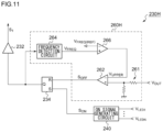
- FIG. 11 is a circuit diagram showing a converter controller 230 H according to an example 1-3.
- the upper limit voltage V UPPER is feedback controlled so as to maintain the switching frequency of the switching transistor M 1 at a constant value.
- An off signal generating circuit 260 H includes a frequency detection circuit 264 and an error amplifier 266 in addition to the comparator 262 .
- the frequency detection circuit 264 monitors the output Q of the logic circuit 234 or the control pulse S 1 , and generates a frequency detection signal V FREQ that indicates the switching frequency.
- the error amplifier 266 amplifies the difference between the frequency detection signal V FREQ and the reference voltage V FREQ(REF) that defines a target value of the switching frequency, and generates the upper limit voltage V UPPER that corresponds to the difference thus amplified.
- this arrangement is capable of stabilizing the switching frequency to a target value. This allows the noise countermeasures to be provided in a simple manner.
- FIG. 12 is a circuit diagram showing a converter controller 230 I according to an example 1-4.
- the converter controller 230 I may turn off the switching transistor M 1 after the on time T ON elapses after the switching transistor M 1 is turned on. That is to say, as the turn-off condition, a condition that the on time T ON elapses after the switching transistor M 1 is turned off may be employed.
- An off signal generating circuit 260 I includes a timer circuit 268 .
- the timer circuit 268 starts the measurement of the predetermined on time T ON in response to the on signal S ON . After the on time T ON elapses, the timer circuit 268 asserts (e.g., sets to the high level) the off signal S OFF .
- the timer circuit 268 may be configured as a monostable multivibrator (one-shot pulse generator), for example. Also, the timer circuit 268 may be configured as a digital counter or an analog timer. In order to detect the timing at which the switching transistor M 1 is turned on, the timer circuit 268 may receive the output Q of the logic circuit 234 or the control pulse S 1 as its input signal instead of the on signal S ON .
- FIG. 13 is a circuit diagram showing a converter controller 230 J according to an example 1-5.
- the converter controller 230 J turns off the switching transistor M 1 after the on time T ON elapses after the switching transistor M 1 is turned on.
- An OR gate 241 corresponds to the on signal generating circuit, and generates the on signal S ON .
- the timer circuit 268 is configured as a monostable multivibrator or the like. The timer circuit 268 generates the pulse signal S P that is set to the high level for a predetermined on time T ON after the assertion of the on signal S ON , and supplies the pulse signal S P to the driver 232 .
- an OR gate 231 is provided as an additional component. With such an arrangement, the logical OR S P ′ of the on signal S ON and the output S P of the timer circuit 268 is supplied to the driver 232 .
- FIG. 14 is a circuit diagram showing a converter controller 230 K according to an example 1-6.
- An off signal generating circuit 260 K feedback controls the on time T ON so as to maintain the switching frequency at a constant value.
- a variable timer circuit 270 is configured as a monostable multivibrator that generates the pulse signal S P that is set to the high level during a period of the on time T ON after the assertion of the on signal S ON .
- the variable timer circuit 270 is configured to change the on time T ON according to a control voltage V CTRL .
- variable timer circuit 270 may include a capacitor, a current source that charges the capacitor, and a comparator that compares the voltage across the capacitor with a threshold value.
- the variable timer circuit 270 is configured such that at least one from among the current amount generated by the current source and the threshold value can be changed according to the control voltage V CTRL .
- the frequency detection circuit 272 monitors the output Q of the logic circuit 234 or the control pulse S 1 , and generates a frequency detection signal V FREQ that indicates the switching frequency.
- An error amplifier 274 amplifiers the difference between the frequency detection signal V FREQ and the reference voltage V FREQ(REF) that defines a target value of the switching frequency, and generates the control voltage V CTRL that corresponds to the difference thus amplified.
- this arrangement is capable of stabilizing the switching frequency to the target value, thereby allowing the noise countermeasures to be provided in a simple manner.
- FIG. 15 is a circuit diagram showing a specific configuration of the converter controller 230 K shown in FIG. 14 . Description will be made regarding the operation of the frequency detection circuit 272 .
- a combination of a capacitor C 11 and a resistor R 11 functions as a high-pass filter, which can be regarded as a differentiating circuit that differentiates the output of the OR gate 231 (or the control pulse S 1 ).
- Such a high-pass filter can also be regarded as an edge detection circuit that detects an edge of the pulse signal S P ′.
- a transistor Tr 11 turns on so as to discharge the capacitor C 12 .
- the capacitor C 12 is charged via a resistor R 12 .
- the voltage V C12 across the capacitor C 12 is configured as a ramp wave in synchronization with the pulse signal S P ′.
- the time length of the slope portion thereof, and the wave height that corresponds to the time length of the slope portion, change according to the period of the pulse signal S P ′.
- a combination of the transistors Tr 12 and Tr 13 , the resistors R 13 and R 14 , and a capacitor C 13 is configured as a peak hold circuit.
- the peak hold circuit holds the peak value of the voltage V C12 across the capacitor C 12 .
- the output V FREQ of the peak hold circuit has a correlation with the period of the pulse signal S P ′, i.e., the frequency thereof.
- a comparator COMP 1 compares the frequency detection signal V FREQ with the reference signal V FREQ(REF) that indicates the target frequency.
- a combination of a resistor R 15 and a capacitor C 14 is configured as a low-pass filter.
- the low-pass filter smooths the output of the comparator COMP 1 so as to generate the control voltage V CTRL .
- the control signal V CTRL is output via a buffer BUF 1 .
- variable timer circuit 270 Description will be made regarding the variable timer circuit 270 .
- the on signal S ON is inverted by an inverter 273 .
- the inverted on signal #S ON becomes lower than a threshold value V TH1 , i.e., when the on signal S ON is set to the high level, the output of a comparator COMP 2 is set to the high level. This sets a flip-flop SREF, thereby setting the pulse signal S P to the high level.
- the transistor M 21 is turned off.
- a current source 271 generates a variable current I VAR that corresponds to the control voltage V CTRL so as to charge a capacitor C 12 .
- the output of the comparator COMP 3 is set to the high level. This resets the flip-flop SREF, thereby switching the pulse signal S P to the low level.
- the transistor M 21 is turned on, thereby initializing the voltage V C15 of the capacitor C 15 .
- FIG. 16 is a circuit diagram showing a modification of the on signal generating circuit 240 .
- the comparator 252 is employed as shown in FIG. 7 .
- this arrangement supports high-precision voltage comparison.
- such an arrangement has a tradeoff problem of a large circuit area and high costs.
- a voltage comparison unit having a simple configuration including a transistor may be employed.
- a voltage comparison unit 253 includes an emitter follower circuit 255 including a PNP bipolar transistor Tr 21 and a comparison circuit 257 .
- the output (V LED +V BE ) of the emitter follower circuit 255 configured as an upstream stage is voltage divided by means of resistors R 21 and R 22 , and then input to the base of a transistor Tr 22 .
- the voltage V LED to be monitored decreases, the base voltage of the transistor Tr 22 decreases.
- the current that flows through the transistor Tr 22 is cut off, which sets the output of the voltage comparison unit 253 to the high level.
- FIG. 16 shows an example in which the outputs of the multiple voltage comparison units 253 are input to the OR gate 254 .
- the present disclosure is not restricted to such an example.
- such an OR gate 254 may be omitted.
- the collectors of the transistors Tr 22 of the multiple voltage comparison units 253 may be coupled so as to form a common collector.
- a common resistor may be provided between the common collector and the power supply line V CC .
- FIGS. 17 A through 17 C are circuit diagrams each showing an example configuration of the current source 210 .
- the current source 210 shown in FIG. 17 A includes a series transistor M 2 , a sensing resistor R S , and an error amplifier 212 .
- the series transistor M 2 and the sensing resistor R S are provided in series on a path of the driving current I LEDi .
- the error amplifier 212 adjusts the voltage V G at a control electrode (gate in this example) of the series transistor M 2 such that the voltage drop V CS that occurs across the sensing resistor R S approaches a target voltage V ADIM .
- the series transistor M 2 is configured as an N-type (N-channel) MOS transistor.
- the error amplifier 212 is arranged such that the reference voltage V ADIM is input to one input thereof (non-inverting input terminal) and such that the voltage V CS (voltage drop that occurs across the sensing resistor R S ) at a connection node that couples the series transistor M 2 and the sensing resistor R S is input to the other input thereof (inverting input terminal).
- the current source 210 further includes a switch (dimming switch) 214 for PWM dimming.
- the dimming switch 214 is controlled according to a PWM signal S PWM generated by the dimming controller 116 .
- the dimming switch 214 is turned off, the driving current I LED flows through the current source 210 .
- the dimming switch 214 is turned on, the series transistor M 2 is turned off, which disconnects the driving current I LED .
- the dimming switch 214 is switched at a high speed at a PWM frequency of 60 Hz or more. Furthermore, by adjusting the duty ratio of the PWM frequency, the semiconductor light source 102 is subjected to PWM dimming control.
- the series transistor is configured as a P-channel MOSFET.
- the error amplifier 212 is configured to have an input polarity that is the reverse of that shown in FIG. 17 A .
- the bottom limit voltage V BOTTOM may preferably be determined as represented by the following Expression.
- ⁇ V represents an appropriate margin.
- V BOTTOM R S ⁇ I LED +V SAT + ⁇ V
- the current source 210 shown in FIG. 17 C has the same configuration as that shown in FIG. 5 , including a current mirror circuit 216 and a reference current source 218 .
- the current mirror circuit 216 multiplies the reference current I REF generated by the reference current source 218 by a predetermined coefficient determined by a mirror ratio, so as to generate the driving current I LED .
- the bottom limit voltage V BOTTOM may preferably be determined as represented by the following Expression.
- V BOTTOM V SAT + ⁇ V
- V SAT represents the saturation voltage of the current mirror circuit
- ⁇ V represents an appropriate margin
- FIG. 18 is a circuit diagram showing a current driver IC 300 and a peripheral circuit thereof according to an embodiment 2.
- the current driver IC 300 includes an interface circuit 320 and a dimming pulse generator 330 .
- the multiple current sources 310 _ 1 through 310 _N are configured to switch independently between the on state and the off state according to PWM signals S PWM1 through S PWMN , respectively.
- the current sources 310 _ 1 through 310 _N are respectively coupled to the corresponding semiconductor light sources 102 _ 1 through 102 _N in series via cathode pins LED 1 through LEDN.
- the interface circuit 320 receives multiple items of control data D 1 through D N from an external microcontroller (processor) 114 .
- the kind of the interface is not restricted in particular.
- a Serial Peripheral Interface (SPI) or I 2 C interface may be employed.
- the multiple items of control data D 1 through D N respectively indicate the on/off duty ratios of the multiple current sources 310 _ 1 through 310 _N, which are updated at a first time interval T 1 .
- the first time interval T 1 is set to on the order of 20 ms to 200 ms. For example, the first time interval T 1 is set to 100 ms.
- the dimming pulse generator 330 generates the multiple PWM signals S PWM1 through S PWMN for the multiple current sources 310 _ 1 through 310 _N based on the multiple items of control data D 1 through D N .
- the microcontroller 114 generates the multiple PWM signals S PWM1 through S PWN .
- the current driver IC 300 has a built-in function of generating the multiple PWM signals S PWM1 through S PWMN .
- the duty ratio of the i-th PWM signal S PWM1 is gradually changed at a second time interval T 2 that is shorter than the first time interval T 1 from the corresponding control data D 1 value before updating to the updated value thereof (which will be referred to as the “gradual-change mode”).
- the second time interval T 2 is set to a value on the order of 1 ms to 10 ms. For example, the second time interval T 2 is set to 5 ms.
- the dimming pulse generator 330 is capable of supporting a non-gradual-change mode in addition to the gradual-change mode.
- the duty ratio of the i-th PWM signal S PWM1 is allowed to be immediately changed from the corresponding control data D i value before updating to the updated value thereof.
- the dimming pulse generator 330 may preferably be configured to dynamically switch its mode between the non-gradual-change mode and the gradual-change mode according to the settings received from the microcontroller 114 .
- the dimming pulse generator 330 is configured to dynamically switch its mode between the non-gradual-change mode and the gradual-change mode for each channel (for each dimming pulse).
- the setting data that indicates the mode may be appended to the control data D i .
- a part of or the whole of the on signal generating circuit 240 may be integrated on the current driver IC 300 .
- the part of the on signal generating circuit 240 to be integrated may preferably be determined according to the circuit configuration of the on signal generating circuit 240 , and specifically, may preferably be determined so as to reduce the number of lines that couple the converter controller 230 and the current driver IC 300 .
- FIG. 18 in a case in which the entire on signal generating circuit 240 is integrated on the current driver IC 300 , such an arrangement requires only a single line between the converter controller 230 and the current driver IC 300 , which is used to transmit the on signal S ON .
- the minimum value circuit 256 is integrated on the current driver IC 300
- such an arrangement requires only a single line between the converter controller 230 and the current driver IC 300 , through which the minimum voltage V MIN propagates.
- FIG. 19 is an operation waveform diagram showing the operation of the current driver IC 300 .
- the duty ratio of the PWM signal is changed linearly.
- the duty ratio may preferably be changed in a stepwise manner with 20 steps.
- the microcontroller 114 must update the control data D 1 through D N that each indicate the duty ratio at the second time interval T 2 .
- the microcontroller 114 In a case in which the number of channels N of the semiconductor light sources 102 exceeds several dozen to 100, such an arrangement requires a high-performance microcontroller, i.e., a high-cost microcontroller, configured as the microcontroller 114 .
- a high-performance microcontroller i.e., a high-cost microcontroller, configured as the microcontroller 114 .
- such an arrangement requires high-speed communication between the microcontroller 114 and the current driver IC 300 , thereby leading to the occurrence of a noise problem.
- this arrangement allows the rate at which the microcontroller 114 updates the control data D 1 through D N to be reduced. This allows the performance required for the microcontroller 114 to be reduced. Furthermore, this allows the communication speed between the microcontroller 114 and the current driver IC 300 to be reduced, thereby solving the noise problem.
- the first time interval T 1 may preferably be configured to be variable. In a situation in which there is only a small change in the duty ratio, the first time interval T 1 is increased so as to reduce the data communication amount, thereby allowing power consumption and noise to be reduced.
- FIG. 19 shows an example in which the duty ratio is changed linearly. Also, the duty ratio may be changed according to a curve function such as a quadratic function or an exponential function. In a case of employing such a quadratic function, this arrangement provides natural dimming control with less discomfort.
- a curve function such as a quadratic function or an exponential function.
- the multiple semiconductor light sources 102 _ 1 through 102 _N may be integrated on a single semiconductor chip (die) 402 .
- the semiconductor chip 402 and the current driver IC 300 may be housed in a single package in the form of a module.
- FIG. 20 shows a plan view and a cross-sectional view of the integrated-driver light source 400 .
- the multiple semiconductor light sources 102 are formed in a matrix on the front face of the semiconductor chip 402 .
- the back face of the semiconductor chip 402 is provided with pairs of back-face electrodes A and K that each correspond to a pair of an anode electrode and a cathode electrode of each of the multiple semiconductor light sources 102 .
- pairs of back-face electrodes A and K that each correspond to a pair of an anode electrode and a cathode electrode of each of the multiple semiconductor light sources 102 .
- only a single connection relation is shown for the semiconductor light source 102 _ 1 .
- the semiconductor chip 402 and the current driver IC 300 are mechanically joined and electrically coupled.
- the front face of the current driver IC 300 is provided with front-face electrodes 410 (LED 1 through LEDN in FIG. 18 ) to be respectively coupled to the cathode electrodes K of the multiple semiconductor light sources 102 and front-face electrodes 412 to be respectively coupled to the anode electrodes A of the multiple semiconductor light sources 102 .
- Each front-face electrode 412 is coupled to a corresponding bump (or pad) 414 provided to a package substrate configured as a back face of the current driver IC 300 .
- an unshown interposer may be arranged between the semiconductor chip 402 and the current driver IC 300 .
- the kind of the package of the integrated-driver light source 400 is not restricted in particular.
- a Ball Grid Array (BAG), Pin Grid Array (PGA), Land Grid Array (LGA), Quad Flat Package (QFP), or the like may be employed.
- a countermeasure may preferably be provided in which a heat dissipation structure or the like is attached to each module.
- the integrated-driver light source 400 as shown in FIG. 20 , there is a need to release the sum total of heat generated by the light sources 102 and the current sources 210 . Accordingly, such an arrangement has the potential to require a very large heat dissipation structure.
- this arrangement is capable of suppressing heat generated by the current sources 210 . This allows the size of the heat dissipation structure to be attached to the integrated-driver light source 400 to be reduced.
- a desired transistor such as the series transistor M 2 may be configured as a bipolar transistor.
- the base corresponds to the gate
- the emitter corresponds to the source
- the collector corresponds to the drain.
- the switching transistor M 1 is configured as a P-channel MOSFET.
- an N-channel MOSFET may be employed.
- a bootstrap circuit may be provided as an additional component.
- an Insulated Gate Bipolar Transistor (IGBT) or a bipolar transistor may be employed.
- FIG. 21 is a circuit diagram showing an automotive lamp 100 according to a modification 1-3.
- the cathodes of the semiconductor light sources 102 are coupled so as to form a common cathode.
- each current source 210 configured as a source circuit is coupled to the anode side of the corresponding semiconductor light source 102 .
- Each current source 210 may be configured by geometrically reversing the configuration of the current source shown in FIG. 5 or 17 .
- the converter controller 230 controls the switching converter 220 based on the relation between the voltages V CS that occur across each current source 210 and the bottom limit voltage V BOTTOM .
- FIG. 24 is a block diagram showing a lamp system 1 including the automotive lamp 100 according to an embodiment 3.
- the lamp system 1 includes a battery 2 , an in-vehicle Electronic Control Unit (ECU) 4 , and an automotive lamp 100 .
- the automotive lamp 100 is configured as a variable light distribution headlamp having an ADB function.
- the automotive lamp 100 generates a light distribution according to a control signal received from the in-vehicle ECU 4 .
- the automotive lamp 100 includes multiple (N ⁇ 2) semiconductor light sources 102 _ 1 through 102 _N, a lamp ECU 110 , a lighting circuit 200 , and a current driver IC 300 .
- Each semiconductor light source 102 may preferably be configured using an LED. Also, various kinds of light-emitting elements such as an LD, organic EL, or the like, may be employed.
- Each semiconductor light source 102 may include multiple light-emitting elements coupled in series and/or coupled in parallel. It should be noted that the number of the semiconductor light sources 102 , i.e., N, is not restricted in particular. Specifically, the number N is at least several dozen or more, and is preferably several hundred to several thousand. Also, the number of channels, i.e., N, may be on the order of tens of thousands.
- the multiple semiconductor light sources 102 _ 1 through 102 _N are integrated on a single semiconductor chip (LED chip 103 ).
- the lamp ECU 110 includes a switch 112 and a microcontroller 114 .
- the microcontroller (processor) 114 is coupled to the in-vehicle ECU 4 via a bus such as a Controller Area Network (CAN) or Local Interconnect Network (LIN) or the like. This allows the microcontroller 114 to receive various kinds of information such as a turn-on/turn-off instruction, etc.
- the microcontroller 114 turns on the switch 112 in response to a turn-on instruction received from the in-vehicle ECU 4 . In this state, a power supply voltage (battery voltage V BAT ) is supplied from the battery 2 to the lighting circuit 200 .
- a power supply voltage battery voltage V BAT
- the microcontroller 114 receives a control signal for indicating the light distribution pattern from the in-vehicle ECU 4 , and controls the lighting circuit 200 . Also, the microcontroller 114 may receive information that indicates the situation ahead of the vehicle from the in-vehicle ECU 4 , and may autonomously generate the light distribution pattern based on the information thus received.
- the current driver IC 300 supplies the driving currents I LED1 through I LEDN to the multiple semiconductor light sources 102 _ 1 through 102 _N.
- the current driver IC 300 is configured to capable of independently turning on and off the driving current I LED for each semiconductor light source 102 .
- the lighting circuit 200 supplies the driving voltage V OUT to the LED chip 103 and the current driver IC 300 .
- the lighting circuit 200 may include the switching converter 220 and the converter controller 230 .
- the switching converter 220 is configured as a step-down converter.
- the topology of the switching converter 220 is not restricted in particular.
- the current driver IC 300 includes multiple current sources 310 _ 1 through 310 _N, an interface circuit 320 , a protection circuit 340 , and a feedback circuit 360 .
- the current source 310 _# (“#” represents 1 through N) is coupled in series with the corresponding one 102 _# from among the multiple semiconductor light sources 102 _ 1 through 102 _N.
- the current source 310 _# is configured to be capable of switching its on/off state according to a control input Sp_#.
- the current source 310 _# When the current source 310 _# is set to the on state, the current source 310 _# generates a driving current I LED# .
- the current source 310 _# When the current source 310 _# is set to the off state, the driving current I LED# is disconnected. For example, when the control input Sp_# is set to the high level, the current source 310 _# is set to the on state. Conversely, when the control input Sp_# is set to the low level, the current source 310 _# is set to the off state.
- FIG. 25 is a circuit diagram showing an example configuration of the multiple current sources 310 .
- Each current source 310 includes a current mirror circuit 312 , a reference current source 314 , and a dimming switch 316 .
- the reference current source 314 generates a reference current I REF .
- the current mirror circuit 312 copies the reference current I REF , so as to generate a driving current I LED .
- the dimming switch 316 is arranged between the gate and the source of the current mirror circuit 312 . When the dimming switch 316 is turned on, the operation of the current mirror circuit 312 is suspended, thereby disconnecting the driving current I LED .
- An inverter 318 inverts the control input Sp, and inputs the inverted control input to the gate of the dimming switch 316 . It should be noted that, in a case of employing a negative logic system, the inverter 318 may be omitted, and the semiconductor light source 102 may be turned on when the control input Sp is set to the low level.
- the feedback circuit 360 outputs a feedback signal S FB to the converter controller 230 according to the voltages V LED1 through V LEDN that respectively occur across the multiple current sources 310 _ 1 through 310 _N.
- the feedback circuit 360 is designed according to a control method of the converter controller 230 .
- the converter controller 230 may support a ripple control operation.
- the feedback circuit 360 may assert the feedback signal S FB .
- the converter controller 230 may turn on the switching transistor M 1 in response to the assertion of the feedback signal S FB .
- the converter controller 230 may support a Pulse Width Modulation (PWM) control operation.
- the feedback circuit 360 may amplify the difference between a predetermined reference voltage V REF and the lowest voltage from among the voltages V LED1 through V LEDN that respectively occur across the current sources 310 _ 1 through 310 _N, so as to generate the feedback signal S FB in the form of an analog signal.
- the converter controller 230 may generate a PWM signal having a duty ratio that corresponds to the voltage level of the feedback signal S FB , so as to drive the switching transistor M 1 .
- the interface circuit 320 is coupled to the microcontroller (processor) 114 , and receives a control signal S 1 that indicates the on/off state of each of the multiple semiconductor light sources 102 _ 1 through 102 _N.
- the interface circuit 320 has a decoder function of converting the control signal S 1 thus received into multiple individual control signals S 2 _ 1 through S 2 _N.
- the multiple individual control signals S 2 _ 1 through S 2 _N determine the on/off state of each of the multiple current sources 310 _ 1 through 310 _N.
- the protection circuit 340 monitors the communication between the microcontroller 114 and the interface circuit 320 .
- the individual control signals S 2 _ 1 through S 2 _N which are generated based on the control signal S 1 , are supplied to the respective current sources 310 _ 1 through 310 _N as they are.
- the protection circuit 340 forcibly sets the multiple current sources 310 _ 1 through 310 _N to a predetermined state.
- the protection circuit 340 replaces the control inputs Sp_ 1 through Sp_N, which are to be supplied to the current sources 310 _ 1 through 310 _N, with a set of predetermined values independent of the control signal S 1 (individual control signals S 2 _ 1 through S 2 _N).
- the predetermined state may correspond to a low-beam light distribution.
- FIG. 26 is a plan view of the LED chip 103 .
- the LED chip 103 is configured as an array of the multiple semiconductor light sources 102 arranged in a matrix form. Each semiconductor light source 102 corresponds to a pixel.
- a region RGN ON to be turned on so as to generate the low-beam light distribution is surrounded by the heavy line.
- the multiple semiconductor light sources 102 included in the region RGN ON are forcibly turned on.
- the multiple semiconductor light sources 102 included in a region to be turned off for the low-beam light distribution are forcibly turned off when judgement has been made that an abnormal state has occurred.
- FIG. 27 is a block diagram showing an example configuration of the interface circuit 320 and the protection circuit 340 .
- the interface circuit 320 may include a shift register 322 with an output latch.
- the interface circuit 320 and the light distribution controller 116 are coupled via three lines, i.e., an SDATA line, SCK line, and RCK line.
- the shift register 322 with an output latch includes an N-bit shift register configured as an input stage and an N-bit storage register configured as an output stage.
- the input-stage shift register acquires serial data SDATA in synchronization with the SCK signal. Furthermore, the value acquired by the shift register is copied to the storage register, and the value is updated, in response to a positive edge of the RCK signal.
- the values stored in the storage register are output as the individual control signals S 2 _ 1 through S 2 _N.
- the protection circuit 340 includes an abnormal state detection circuit 342 and a data replacement circuit 344 .
- the abnormal state detection circuit 342 monitors at least one from among the input signals of the interface circuit 320 (SDATA, SCK, RCK, in this example), in order to detect the occurrence of an abnormal state in the communication. For example, when there is no change in a signal to be monitored for a predetermined period of time, the interface circuit 320 may judge that an abnormal state has occurred. When judgement has been made that an abnormal state has occurred, an abnormal state detection signal S 3 is asserted.
- the data replacement circuit 344 When the abnormal state detection signal S 3 is negated, the data replacement circuit 344 outputs the individual control signals S 2 _ 1 through S 2 _N as they are. When the abnormal state detection signal S 3 is asserted, the data replacement circuit 344 replaces the control inputs Sp_ 1 through Sp_N for respectively controlling the multiple current sources 310 _ 1 through 310 _N with predetermined values specified for the respective semiconductor light sources. Specifically, the input control Sp is set to “H” for each semiconductor light source 102 to be turned on in the abnormal state. On the other hand, for each semiconductor light source 102 to be turned off in the abnormal state, the input control Sp is set to “L”.
- FIGS. 28 A and 28 B are circuit diagrams each showing an example configuration of the data replacement circuit 344 .
- the data replacement circuit 344 shown in FIG. 28 A includes an inverter 346 , multiple first logic gates 348 , and multiple second logic gates 350 .
- the inverter 346 inverts the abnormal state detection signal S 3 so as to generate an inverted abnormal state detection signal S 3 b .
- the multiple first logic gates 348 respectively correspond to multiple current sources to be turned on in the abnormal state from among the multiple current sources 310 .
- Each first logic gate 348 _ i receives the corresponding individual control signal S 2 _ i and one (S 3 in this example) from among the abnormal state detection signal S 3 and the inverted abnormal state detection signal S 3 b , and supplies its output to the corresponding current source 310 _ i .
- the first logic gate 348 is configured as an OR gate.
- the multiple second logic gates 350 correspond to multiple current sources to be turned off in the abnormal state from among the multiple current sources 310 .
- Each second logic gate 350 _ j receives the corresponding individual control signal S 2 _ j and the other one (S 3 b in this example) from among the abnormal state detection signal S 3 and the inverted abnormal state detection signal S 3 b , and supplies its output to the corresponding current source 310 _ j .
- the second logic gate 350 is configured as an AND gate.
- FIG. 28 B shows another example configuration of the data replacement circuit 344 .
- the data replacement circuit 344 includes multiple selectors 352 _ 1 through 352 _N that correspond to the multiple current sources 310 _ 1 through 310 _N.
- Each selector 352 _# receives the corresponding individual control signal S 2 _# and a predetermined value a# as its input signals.
- the predetermined value a# is set to 1 for each of the current sources 310 _ i to be turned on in the abnormal state.
- the predetermined value a# is set to 0.
- the selector 352 _# selects the individual control signal S 2 _#. Conversely, when the abnormal state detection signal S 3 is asserted (1), the selector 352 _# selects the predetermined value a#.
- Such an arrangement shown in FIG. 28 B requires memory for storing the predetermined values al through a#. However, such an arrangement has an advantage of allowing the light distribution pattern to be generated in the abnormal state to be changed according to the value stored in the memory. In contrast, an arrangement shown in FIG. 28 A has no function of changing the light distribution pattern to be generated in the abnormal state. However, such an arrangement does not require memory, thereby allowing the circuit area to be reduced.
- FIG. 29 shows a plan view and a cross-sectional view of the integrated-driver light source 400 .
- the multiple semiconductor light sources 102 are formed in a matrix on the front face of the semiconductor chip 402 (LED chip in FIG. 24 ).
- the back face of the semiconductor chip 402 is provided with pairs of back-face electrodes A and K that each correspond to a pair of an anode electrode and a cathode electrode of each of the multiple semiconductor light sources 102 .
- the semiconductor light source 102 _ 1 only a single connection relation is shown for the semiconductor light source 102 _ 1 .
- the semiconductor chip 402 and the current driver IC 300 are mechanically joined and electrically coupled.
- the front face of the current driver IC 300 is provided with front-face electrodes 410 to be respectively coupled to the cathode electrodes K of the multiple semiconductor light sources 102 and front-face electrodes 412 to be respectively coupled to the anode electrodes A of the multiple semiconductor light sources 102 .
- Each front-face electrode 412 is coupled to a corresponding bump (or pad) 414 provided to a package substrate configured as a back face of the current driver IC 300 .
- an unshown interposer may be arranged between the semiconductor chip 402 and the current driver IC 300 .
- the kind of the package of the integrated-driver light source 400 is not restricted in particular.
- a Ball Grid Array (BAG), Pin Grid Array (PGA), Land Grid Array (LGA), Quad Flat Package (QFP), or the like may be employed.
- FIG. 30 is a circuit diagram showing an automotive lamp 100 according to a modification 3.1.
- the cathodes of the semiconductor light sources 102 are coupled so as to form a common cathode.
- the current sources 310 configured as source circuits are coupled to the anode sides of the corresponding semiconductor light sources 102 .
- the difference between V OUT and V LED# matches the voltage across the current source 310 _#.
- V MIN represents a minimum value of the voltage across the current source 310 which enables the operation of the current source 310 .
- the converter controller 230 may turn on the switching transistor M 1 in response to assertion of the feedback signal S FB .
- the switching transistor M 1 is configured as a P-channel MOSFET.
- the switching transistor M 1 may be configured as an N-channel MOSFET.
- a bootstrap circuit may be provided as an additional circuit.
- an Insulated Gate Bipolar Transistor (IGBT) or a bipolar transistor may be employed.
- the configuration of the current source 310 is not restricted to such an arrangement employing a current mirror circuit. Also, various kinds of known configurations may be employed.
- FIG. 31 is a block diagram showing an automotive lamp 500 according to an embodiment 4.
- a lighting circuit 570 turns on a light source 560 .
- a variable light distribution device 530 includes multiple elements that can be controlled independently. The light distribution pattern is generated according to a state of the multiple controllable elements.
- the variable light distribution device 530 is configured as a Digital Mirror Device (DMD) that reflects the output light of the light source 560 or multiple bypass switches.
- DMD Digital Mirror Device
- a lamp ECU 510 is configured as a higher-level controller that controls the light distribution pattern based on a control signal received from the in-vehicle ECU 4 via the communication line 5 and various kinds of information.
- a local controller 540 and the variable light distribution device 530 are mounted on a single substrate 504 .
- An interface circuit 520 is coupled to the lamp ECU 510 via a communication line 502 .
- the interface circuit 520 receives the control signal S 1 that indicates the light distribution pattern.
- the local controller 540 controls the variable light distribution device 530 based on the control signal S 1 received by the interface circuit 520 .
- the local controller 540 may have a decoder function of converting the control signal S 1 received from the lamp ECU 510 into a control signal S 4 for controlling the variable light distribution device 530 .
- the control signal S 4 may include multiple individual control signals that indicate the respective states of the multiple controllable elements that form the variable light distribution device 530 .
- An abnormal state detection unit 550 monitors communication between the lamp ECU 510 and the interface circuit 520 , and detects an abnormal state based on the monitoring results.
- the automotive lamp 500 is configured such that, when an abnormal state has been detected by the abnormal state detection unit 550 , a predetermined pattern is forcibly set for the variable light distribution device 530 .
- the abnormal state detection unit 550 Upon detecting an abnormal state, the abnormal state detection unit 550 asserts an abnormal state detection signal S 5 . For example, when there is no change in the control signal S 1 transmitted via the communication line 502 for a predetermined period of time, the abnormal state detection unit 550 may judge that an abnormal state has occurred. In response to the assertion of the abnormal state detection signal S 5 , the local controller 540 sets the multiple individual control signals S 2 to a set of predetermined values.
- the interface circuit 520 , the local controller 540 , and the abnormal state detection unit 550 may be configured as a single microcontroller. Also, the interface circuit 520 , the local controller 540 , and the abnormal state detection unit 550 may be configured as a combination of multiple hardware components.
- the embodiment 3 can be regarded as a form of the embodiment 4, and there is the following correspondence between them.
- the interface circuit 320 shown in FIG. 24 corresponds to the interface circuit 520 and the local controller 540 shown in FIG. 31 .
- the multiple current sources 310 _ 1 through 310 _N (or the multiple dimming switches 316 included in the current sources 310 _ 1 through 310 _M) shown in FIG. 24 correspond to the variable light distribution device 530 shown in FIG. 31 .
- the abnormal state detection circuit 342 shown in FIG. 27 corresponds to the abnormal state detection unit 550 shown in FIG. 31 .
- the data replacement circuit 344 shown in FIG. 27 corresponds to a part of the local controller 540 shown in FIG. 31 .
- FIG. 32 is a block diagram showing an automotive lamp 500 A according to a modification 4.1.
- the automotive lamp 500 A further includes a selector 552 and a fixed light distribution instruction unit 554 in addition to the components of the automotive lamp 500 shown in FIG. 31 .
- the fixed light distribution instruction unit 554 generates a control signal S 6 for determining a light distribution pattern to be used in an abnormal state.
- the selector 552 selects the control signal S 4 generated by the local controller 540 .
- the selector 552 selects the control signal S 6 generated by the fixed light distribution instruction unit 554 .
- FIG. 33 is a block diagram showing an automotive lamp 500 B according to a modification 4.2.
- the automotive lamp 500 B further includes a second abnormal state detection unit 556 in addition to the components included in the automotive lamp 500 shown in FIG. 32 .
- the second abnormal state detection unit 556 monitors the output S 4 of the local controller 540 . Upon detecting an abnormal state, the second abnormal state detection unit 556 asserts an abnormal state detection signal S 7 .
- the local controller 540 In response to the assertion of the abnormal state detection signal S 5 , the local controller 540 replaces the control signal S 4 with a signal to be used in the abnormal state.
- the abnormal state detection signal S 7 when the abnormal state detection signal S 7 is asserted, this means that the local controller 540 is not operating normally, or that an abnormal state has occurred in the communication line between the local controller 540 and the variable light distribution device 530 . In this state, such an arrangement is not able to supply the control signal S 4 to be used in the abnormal state to the variable light distribution device 530 . Accordingly, when the abnormal state detection signal S 7 is asserted, the selector 552 selects the control signal S 6 generated by the fixed light distribution instruction unit 554 . This allows a suitable control signal to be supplied to the variable light distribution device 530 .
Abstract
Description
V OUT >V Fi +V SATi (1)
V OUT(REF) =V F(MARGIN) +V SAT(MARGIN) (2)
V LED1 =V OUT −V F1
V LED2 =V OUT −V F2
V LED3 =V OUT −V F3
V OD =V GS −V GS(th)
V BOTTOM =V CONST +I COMP ×R 51
V D =R ON ×I C
V BOTTOM =R S ×I LED +V SAT +ΔV
V BOTTOM =V SAT +ΔV
Claims (4)
Priority Applications (1)
| Application Number | Priority Date | Filing Date | Title |
|---|---|---|---|
| US17/402,941 US11602029B2 (en) | 2018-04-10 | 2021-08-16 | Automotive lamp |
Applications Claiming Priority (9)
| Application Number | Priority Date | Filing Date | Title |
|---|---|---|---|
| JPJP2018-075581 | 2018-04-10 | ||
| JP2018-075581 | 2018-04-10 | ||
| JP2018075581 | 2018-04-10 | ||
| JP2018078332 | 2018-04-16 | ||
| JP2018-078332 | 2018-04-16 | ||
| JPJP2018-078332 | 2018-04-16 | ||
| PCT/JP2019/014888 WO2019198604A1 (en) | 2018-04-10 | 2019-04-03 | Vehicle lamp, lighting circuit therefor, driver circuit, and driver-integrated light source |
| US17/064,695 US11612034B2 (en) | 2018-04-10 | 2020-10-07 | Automotive lamp |
| US17/402,941 US11602029B2 (en) | 2018-04-10 | 2021-08-16 | Automotive lamp |
Related Parent Applications (1)
| Application Number | Title | Priority Date | Filing Date |
|---|---|---|---|
| US17/064,695 Division US11612034B2 (en) | 2018-04-10 | 2020-10-07 | Automotive lamp |
Publications (2)
| Publication Number | Publication Date |
|---|---|
| US20210378070A1 US20210378070A1 (en) | 2021-12-02 |
| US11602029B2 true US11602029B2 (en) | 2023-03-07 |
Family
ID=68164130
Family Applications (2)
| Application Number | Title | Priority Date | Filing Date |
|---|---|---|---|
| US17/064,695 Active US11612034B2 (en) | 2018-04-10 | 2020-10-07 | Automotive lamp |
| US17/402,941 Active US11602029B2 (en) | 2018-04-10 | 2021-08-16 | Automotive lamp |
Family Applications Before (1)
| Application Number | Title | Priority Date | Filing Date |
|---|---|---|---|
| US17/064,695 Active US11612034B2 (en) | 2018-04-10 | 2020-10-07 | Automotive lamp |
Country Status (4)
| Country | Link |
|---|---|
| US (2) | US11612034B2 (en) |
| JP (1) | JP7237938B2 (en) |
| CN (2) | CN115529691A (en) |
| WO (1) | WO2019198604A1 (en) |
Families Citing this family (7)
| Publication number | Priority date | Publication date | Assignee | Title |
|---|---|---|---|---|
| CN115529691A (en) | 2018-04-10 | 2022-12-27 | 株式会社小糸制作所 | Vehicle lamp, drive circuit, and drive integrated light source |
| EP3997962B1 (en) * | 2019-07-09 | 2024-02-28 | Signify Holding B.V. | A method of controlling a lighting arrangement, a lighting control circuit and a lighting system |
| EP4164342A4 (en) * | 2020-06-09 | 2024-01-03 | Koito Mfg Co Ltd | Light fixture system for vehicle, and light distribution controller |
| WO2022270415A1 (en) * | 2021-06-22 | 2022-12-29 | 株式会社小糸製作所 | Light distribution controller and vehicle light system |
| JP2023043322A (en) * | 2021-09-16 | 2023-03-29 | ローム株式会社 | Light-emitting element drive device |
| FR3129639A1 (en) * | 2021-11-26 | 2023-06-02 | Grupo Antolin Besancon | Automotive vehicle ambient lighting system |
| EP4245606A1 (en) | 2022-03-16 | 2023-09-20 | ZKW Group GmbH | Method for controlling an adaptive motor vehicle headlamp |
Citations (22)
| Publication number | Priority date | Publication date | Assignee | Title |
|---|---|---|---|---|
| JP2007200828A (en) | 2006-01-27 | 2007-08-09 | Okazumi Kogyo Kk | Light-emitting diode lighting circuit |
| US20070195025A1 (en) | 2006-02-23 | 2007-08-23 | Powerdsine, Ltd. - Microsemi Corporation | Voltage Controlled Backlight Driver |
| CN101069339A (en) | 2004-12-03 | 2007-11-07 | 罗姆股份有限公司 | Power supply device, light emitting device using such power supply device, and electronic device |
| US20090009088A1 (en) | 2007-07-06 | 2009-01-08 | Koito Manufacturing Co., Ltd. | Lighting control device of lighting device for vehicle |
| JP2010177531A (en) | 2009-01-30 | 2010-08-12 | Texas Instr Japan Ltd | Light emitting diode control device |
| EP2244537A2 (en) | 2009-04-24 | 2010-10-27 | Koito Manufacturing Co., Ltd. | Light source lighting circuit |
| US20110109231A1 (en) | 2009-11-12 | 2011-05-12 | Green Solution Technology Co., Ltd. | Led current control circuit, current balancer and driving apparatus |
| US20110109243A1 (en) | 2009-11-09 | 2011-05-12 | Yong-Hun Kim | Circuit and method of driving light emitting diodes, and light emitting diode system having the same |
| CN102869155A (en) | 2012-09-06 | 2013-01-09 | 上海晶丰明源半导体有限公司 | LED (light-emitting diode) driving source control circuit and control method thereof |
| US20130038819A1 (en) | 2010-02-26 | 2013-02-14 | Rohm Co., Ltd. | Driving circuit for light emitting element, light emitting device using same, and display apparatus |
| US20130062936A1 (en) * | 2011-09-13 | 2013-03-14 | Omron Automotive Electronics Co., Ltd. | Load control device |
| US20140167630A1 (en) * | 2012-12-17 | 2014-06-19 | Power Forest Technology Corporation | Light emitting diode backlight system the driving apparatus and driving method thereof |
| US20140354188A1 (en) | 2013-05-31 | 2014-12-04 | Toshiba Lighting & Technology Corporation | Remote Monitoring Systems |
| US20150032329A1 (en) * | 2013-07-25 | 2015-01-29 | Yazaki Corporation | In-vehicle load control system |
| JP2015138763A (en) | 2014-01-24 | 2015-07-30 | 株式会社小糸製作所 | Vehicular lamp fitting |
| US20160381748A1 (en) | 2015-06-23 | 2016-12-29 | Rohm Co., Ltd. | Control circuit and control method for illumination apparatus |
| US20170359868A1 (en) * | 2014-12-30 | 2017-12-14 | Silicon Works Co., Ltd. | Lamp control device |
| JP2018019025A (en) | 2016-07-29 | 2018-02-01 | 株式会社デンソーテン | Voltage conversion circuit, LED drive circuit and control method of voltage conversion circuit |
| US20180070416A1 (en) * | 2016-09-08 | 2018-03-08 | Panasonic Intellectual Property Management Co., Ltd. | Lighting device, luminaire, vehicle with same, and control method |
| US20180317292A1 (en) | 2017-04-26 | 2018-11-01 | Rohm Co., Ltd. | Light emitting element driving apparatus and driving method thereof |
| US20210016706A1 (en) | 2018-04-10 | 2021-01-21 | Koito Manufacturing Co., Ltd. | Automotive lamp |
| US20210373070A1 (en) | 2020-05-28 | 2021-12-02 | Samsung Electronics Co., Ltd. | Burn in board test device and system |
Family Cites Families (3)
| Publication number | Priority date | Publication date | Assignee | Title |
|---|---|---|---|---|
| JP5730520B2 (en) * | 2010-09-03 | 2015-06-10 | スパンション エルエルシー | Switching regulator |
| JP5367883B2 (en) * | 2011-08-11 | 2013-12-11 | シャープ株式会社 | Illumination device and display device including the same |
| DE102013216155A1 (en) * | 2013-08-14 | 2015-02-19 | Osram Gmbh | Electronic ballast for operating at least a first cascade of LEDs |
-
2019
- 2019-04-03 CN CN202211183907.7A patent/CN115529691A/en active Pending
- 2019-04-03 CN CN201980024538.7A patent/CN111955055B/en active Active
- 2019-04-03 JP JP2020513228A patent/JP7237938B2/en active Active
- 2019-04-03 WO PCT/JP2019/014888 patent/WO2019198604A1/en active Application Filing
-
2020
- 2020-10-07 US US17/064,695 patent/US11612034B2/en active Active
-
2021
- 2021-08-16 US US17/402,941 patent/US11602029B2/en active Active
Patent Citations (28)
| Publication number | Priority date | Publication date | Assignee | Title |
|---|---|---|---|---|
| CN101069339A (en) | 2004-12-03 | 2007-11-07 | 罗姆股份有限公司 | Power supply device, light emitting device using such power supply device, and electronic device |
| JP2007200828A (en) | 2006-01-27 | 2007-08-09 | Okazumi Kogyo Kk | Light-emitting diode lighting circuit |
| US20070195025A1 (en) | 2006-02-23 | 2007-08-23 | Powerdsine, Ltd. - Microsemi Corporation | Voltage Controlled Backlight Driver |
| US20090009088A1 (en) | 2007-07-06 | 2009-01-08 | Koito Manufacturing Co., Ltd. | Lighting control device of lighting device for vehicle |
| JP2009012669A (en) | 2007-07-06 | 2009-01-22 | Koito Mfg Co Ltd | Lighting control device for vehicular light |
| US20100219773A1 (en) | 2009-01-30 | 2010-09-02 | Texas Instruments Incorporated | Light-emitting diode controller |
| JP2010177531A (en) | 2009-01-30 | 2010-08-12 | Texas Instr Japan Ltd | Light emitting diode control device |
| EP2244537A2 (en) | 2009-04-24 | 2010-10-27 | Koito Manufacturing Co., Ltd. | Light source lighting circuit |
| US20110109243A1 (en) | 2009-11-09 | 2011-05-12 | Yong-Hun Kim | Circuit and method of driving light emitting diodes, and light emitting diode system having the same |
| US20110109231A1 (en) | 2009-11-12 | 2011-05-12 | Green Solution Technology Co., Ltd. | Led current control circuit, current balancer and driving apparatus |
| JP2016029665A (en) | 2010-02-26 | 2016-03-03 | ローム株式会社 | Semiconductor chip and light emitting device using the same, and display device |
| US20130038819A1 (en) | 2010-02-26 | 2013-02-14 | Rohm Co., Ltd. | Driving circuit for light emitting element, light emitting device using same, and display apparatus |
| US20130062936A1 (en) * | 2011-09-13 | 2013-03-14 | Omron Automotive Electronics Co., Ltd. | Load control device |
| CN102869155A (en) | 2012-09-06 | 2013-01-09 | 上海晶丰明源半导体有限公司 | LED (light-emitting diode) driving source control circuit and control method thereof |
| US20140167630A1 (en) * | 2012-12-17 | 2014-06-19 | Power Forest Technology Corporation | Light emitting diode backlight system the driving apparatus and driving method thereof |
| US20140354188A1 (en) | 2013-05-31 | 2014-12-04 | Toshiba Lighting & Technology Corporation | Remote Monitoring Systems |
| JP2014236302A (en) | 2013-05-31 | 2014-12-15 | 東芝ライテック株式会社 | Remote monitoring system |
| US20150032329A1 (en) * | 2013-07-25 | 2015-01-29 | Yazaki Corporation | In-vehicle load control system |
| JP2015138763A (en) | 2014-01-24 | 2015-07-30 | 株式会社小糸製作所 | Vehicular lamp fitting |
| US20150211703A1 (en) | 2014-01-24 | 2015-07-30 | Koito Manufacturing Co., Ltd. | Vehicular lamp |
| US20170359868A1 (en) * | 2014-12-30 | 2017-12-14 | Silicon Works Co., Ltd. | Lamp control device |
| US20160381748A1 (en) | 2015-06-23 | 2016-12-29 | Rohm Co., Ltd. | Control circuit and control method for illumination apparatus |
| JP2017010810A (en) | 2015-06-23 | 2017-01-12 | ローム株式会社 | Luminaire, control circuit for the same, control method and display device using the same |
| JP2018019025A (en) | 2016-07-29 | 2018-02-01 | 株式会社デンソーテン | Voltage conversion circuit, LED drive circuit and control method of voltage conversion circuit |
| US20180070416A1 (en) * | 2016-09-08 | 2018-03-08 | Panasonic Intellectual Property Management Co., Ltd. | Lighting device, luminaire, vehicle with same, and control method |
| US20180317292A1 (en) | 2017-04-26 | 2018-11-01 | Rohm Co., Ltd. | Light emitting element driving apparatus and driving method thereof |
| US20210016706A1 (en) | 2018-04-10 | 2021-01-21 | Koito Manufacturing Co., Ltd. | Automotive lamp |
| US20210373070A1 (en) | 2020-05-28 | 2021-12-02 | Samsung Electronics Co., Ltd. | Burn in board test device and system |
Non-Patent Citations (7)
| Title |
|---|
| Final Official Action issued in corresponding U.S. Appl. No. 17/064,695, dated Nov. 26, 2021 (10 pages). |
| First Office Action dated May 13, 2022, issued in the corresponding Chinese Patent Application No. 201980024538.7, 19 pages including 11 pages of English Translation. |
| International Preliminary Report on Patentability (Form PCT/IB/373) and the Written Opinion of the International Searching Authority (Form PCT/ISA/237) dated Oct. 13, 2020, in International Application No. PCT/JP2019/014888. (14 pages). |
| International Search Report (Form PCT/ISA/210) dated Jun. 18, 2019, in International Application No. PCT/JP2019/014888. (4 pages). |
| Notification of Reasons for Refusal dated Sep. 6, 2022, issued in the corresponding Japanese Patent Application No. 2020-513228, 7 pages including 4 pages of English Translation. |
| Office Action issued by the U.S. Patent and Trademark Office in the U.S. Appl. No. 17/064,695, dated Apr. 5, 2022, U.S. Patent and Trademark Office, Alexandria, VA. (14 pages). |
| Official Action issued in U.S. Appl. No. 17/064,695, dated Jul. 22, 2022 (14 pages). |
Also Published As
| Publication number | Publication date |
|---|---|
| CN111955055B (en) | 2023-02-28 |
| JP7237938B2 (en) | 2023-03-13 |
| CN111955055A (en) | 2020-11-17 |
| US20210378070A1 (en) | 2021-12-02 |
| JPWO2019198604A1 (en) | 2021-04-15 |
| US20210016706A1 (en) | 2021-01-21 |
| US11612034B2 (en) | 2023-03-21 |
| CN115529691A (en) | 2022-12-27 |
| WO2019198604A1 (en) | 2019-10-17 |
Similar Documents
| Publication | Publication Date | Title |
|---|---|---|
| US11602029B2 (en) | Automotive lamp | |
| US11558943B2 (en) | Lighting circuit of automotive lamp | |
| US9277615B2 (en) | LED drive circuit | |
| CN109076676B (en) | L ED current controller | |
| WO2020166451A1 (en) | Vehicle lighting fixture, lighting circuit for same, and dc/dc converter control circuit | |
| JP6916668B2 (en) | Lighting circuit for vehicle lighting equipment and light source | |
| JP2004119422A (en) | Light emitting device drive circuit | |
| US20150069906A1 (en) | Circuit arrangement, lighting unit for a vehicle and method for driving semiconductor lighting elements | |
| CN110278626B (en) | Light emitting diode driver for load change | |
| KR20210123224A (en) | Smart flicker-free pwm generation for multi-channel led drivers | |
| US10568168B1 (en) | Lighting system | |
| US20200120767A1 (en) | Vehicle lamp and lighting circuit | |
| US11906123B2 (en) | Light source module | |
| US9030115B2 (en) | LED driver with diac-based switch control and dimmable LED driver | |
| US20240042862A1 (en) | Automotive lamp | |
| US20230093633A1 (en) | Automotive lamp system | |
| US20230104593A1 (en) | Light source module and lighting circuit | |
| JP2015147445A (en) | Vehicle lighting appliance and its drive device | |
| CN111934764A (en) | Driver of visible light communication system |
Legal Events
| Date | Code | Title | Description |
|---|---|---|---|
| AS | Assignment |
Owner name: KOITO MANUFACTURING CO., LTD., JAPAN Free format text: ASSIGNMENT OF ASSIGNORS INTEREST;ASSIGNORS:ICHIKAWA, TOMOYUKI;KIKUCHI, SATOSHI;MATSUHANA, RYOSUKE;SIGNING DATES FROM 20200928 TO 20200930;REEL/FRAME:057188/0970 |
|
| FEPP | Fee payment procedure |
Free format text: ENTITY STATUS SET TO UNDISCOUNTED (ORIGINAL EVENT CODE: BIG.); ENTITY STATUS OF PATENT OWNER: LARGE ENTITY |
|
| STPP | Information on status: patent application and granting procedure in general |
Free format text: DOCKETED NEW CASE - READY FOR EXAMINATION |
|
| STPP | Information on status: patent application and granting procedure in general |
Free format text: NON FINAL ACTION MAILED |
|
| STPP | Information on status: patent application and granting procedure in general |
Free format text: RESPONSE TO NON-FINAL OFFICE ACTION ENTERED AND FORWARDED TO EXAMINER |
|
| STPP | Information on status: patent application and granting procedure in general |
Free format text: FINAL REJECTION MAILED |
|
| STPP | Information on status: patent application and granting procedure in general |
Free format text: NOTICE OF ALLOWANCE MAILED -- APPLICATION RECEIVED IN OFFICE OF PUBLICATIONS |
|
| STCF | Information on status: patent grant |
Free format text: PATENTED CASE |