US11586364B2 - Memory management method, memory storage device and memory control circuit unit - Google Patents
Memory management method, memory storage device and memory control circuit unit Download PDFInfo
- Publication number
- US11586364B2 US11586364B2 US16/779,675 US202016779675A US11586364B2 US 11586364 B2 US11586364 B2 US 11586364B2 US 202016779675 A US202016779675 A US 202016779675A US 11586364 B2 US11586364 B2 US 11586364B2
- Authority
- US
- United States
- Prior art keywords
- read
- error bit
- control circuit
- memory
- read count
- Prior art date
- Legal status (The legal status is an assumption and is not a legal conclusion. Google has not performed a legal analysis and makes no representation as to the accuracy of the status listed.)
- Active, expires
Links
Images


Classifications
-
- G—PHYSICS
- G11—INFORMATION STORAGE
- G11C—STATIC STORES
- G11C29/00—Checking stores for correct operation ; Subsequent repair; Testing stores during standby or offline operation
- G11C29/52—Protection of memory contents; Detection of errors in memory contents
-
- G—PHYSICS
- G06—COMPUTING OR CALCULATING; COUNTING
- G06F—ELECTRIC DIGITAL DATA PROCESSING
- G06F3/00—Input arrangements for transferring data to be processed into a form capable of being handled by the computer; Output arrangements for transferring data from processing unit to output unit, e.g. interface arrangements
- G06F3/06—Digital input from, or digital output to, record carriers, e.g. RAID, emulated record carriers or networked record carriers
- G06F3/0601—Interfaces specially adapted for storage systems
- G06F3/0602—Interfaces specially adapted for storage systems specifically adapted to achieve a particular effect
- G06F3/0604—Improving or facilitating administration, e.g. storage management
-
- G—PHYSICS
- G06—COMPUTING OR CALCULATING; COUNTING
- G06F—ELECTRIC DIGITAL DATA PROCESSING
- G06F3/00—Input arrangements for transferring data to be processed into a form capable of being handled by the computer; Output arrangements for transferring data from processing unit to output unit, e.g. interface arrangements
- G06F3/06—Digital input from, or digital output to, record carriers, e.g. RAID, emulated record carriers or networked record carriers
- G06F3/0601—Interfaces specially adapted for storage systems
- G06F3/0628—Interfaces specially adapted for storage systems making use of a particular technique
- G06F3/0629—Configuration or reconfiguration of storage systems
- G06F3/0632—Configuration or reconfiguration of storage systems by initialisation or re-initialisation of storage systems
-
- G—PHYSICS
- G06—COMPUTING OR CALCULATING; COUNTING
- G06F—ELECTRIC DIGITAL DATA PROCESSING
- G06F11/00—Error detection; Error correction; Monitoring
- G06F11/07—Responding to the occurrence of a fault, e.g. fault tolerance
- G06F11/16—Error detection or correction of the data by redundancy in hardware
- G06F11/20—Error detection or correction of the data by redundancy in hardware using active fault-masking, e.g. by switching out faulty elements or by switching in spare elements
- G06F11/2053—Error detection or correction of the data by redundancy in hardware using active fault-masking, e.g. by switching out faulty elements or by switching in spare elements where persistent mass storage functionality or persistent mass storage control functionality is redundant
- G06F11/2094—Redundant storage or storage space
-
- G—PHYSICS
- G06—COMPUTING OR CALCULATING; COUNTING
- G06F—ELECTRIC DIGITAL DATA PROCESSING
- G06F3/00—Input arrangements for transferring data to be processed into a form capable of being handled by the computer; Output arrangements for transferring data from processing unit to output unit, e.g. interface arrangements
- G06F3/06—Digital input from, or digital output to, record carriers, e.g. RAID, emulated record carriers or networked record carriers
- G06F3/0601—Interfaces specially adapted for storage systems
- G06F3/0602—Interfaces specially adapted for storage systems specifically adapted to achieve a particular effect
- G06F3/061—Improving I/O performance
-
- G—PHYSICS
- G06—COMPUTING OR CALCULATING; COUNTING
- G06F—ELECTRIC DIGITAL DATA PROCESSING
- G06F3/00—Input arrangements for transferring data to be processed into a form capable of being handled by the computer; Output arrangements for transferring data from processing unit to output unit, e.g. interface arrangements
- G06F3/06—Digital input from, or digital output to, record carriers, e.g. RAID, emulated record carriers or networked record carriers
- G06F3/0601—Interfaces specially adapted for storage systems
- G06F3/0602—Interfaces specially adapted for storage systems specifically adapted to achieve a particular effect
- G06F3/0614—Improving the reliability of storage systems
- G06F3/0619—Improving the reliability of storage systems in relation to data integrity, e.g. data losses, bit errors
-
- G—PHYSICS
- G06—COMPUTING OR CALCULATING; COUNTING
- G06F—ELECTRIC DIGITAL DATA PROCESSING
- G06F3/00—Input arrangements for transferring data to be processed into a form capable of being handled by the computer; Output arrangements for transferring data from processing unit to output unit, e.g. interface arrangements
- G06F3/06—Digital input from, or digital output to, record carriers, e.g. RAID, emulated record carriers or networked record carriers
- G06F3/0601—Interfaces specially adapted for storage systems
- G06F3/0628—Interfaces specially adapted for storage systems making use of a particular technique
- G06F3/0629—Configuration or reconfiguration of storage systems
-
- G—PHYSICS
- G06—COMPUTING OR CALCULATING; COUNTING
- G06F—ELECTRIC DIGITAL DATA PROCESSING
- G06F3/00—Input arrangements for transferring data to be processed into a form capable of being handled by the computer; Output arrangements for transferring data from processing unit to output unit, e.g. interface arrangements
- G06F3/06—Digital input from, or digital output to, record carriers, e.g. RAID, emulated record carriers or networked record carriers
- G06F3/0601—Interfaces specially adapted for storage systems
- G06F3/0628—Interfaces specially adapted for storage systems making use of a particular technique
- G06F3/0653—Monitoring storage devices or systems
-
- G—PHYSICS
- G06—COMPUTING OR CALCULATING; COUNTING
- G06F—ELECTRIC DIGITAL DATA PROCESSING
- G06F3/00—Input arrangements for transferring data to be processed into a form capable of being handled by the computer; Output arrangements for transferring data from processing unit to output unit, e.g. interface arrangements
- G06F3/06—Digital input from, or digital output to, record carriers, e.g. RAID, emulated record carriers or networked record carriers
- G06F3/0601—Interfaces specially adapted for storage systems
- G06F3/0628—Interfaces specially adapted for storage systems making use of a particular technique
- G06F3/0655—Vertical data movement, i.e. input-output transfer; data movement between one or more hosts and one or more storage devices
- G06F3/0659—Command handling arrangements, e.g. command buffers, queues, command scheduling
-
- G—PHYSICS
- G06—COMPUTING OR CALCULATING; COUNTING
- G06F—ELECTRIC DIGITAL DATA PROCESSING
- G06F3/00—Input arrangements for transferring data to be processed into a form capable of being handled by the computer; Output arrangements for transferring data from processing unit to output unit, e.g. interface arrangements
- G06F3/06—Digital input from, or digital output to, record carriers, e.g. RAID, emulated record carriers or networked record carriers
- G06F3/0601—Interfaces specially adapted for storage systems
- G06F3/0668—Interfaces specially adapted for storage systems adopting a particular infrastructure
- G06F3/0671—In-line storage system
- G06F3/0673—Single storage device
- G06F3/0679—Non-volatile semiconductor memory device, e.g. flash memory, one time programmable memory [OTP]
-
- G—PHYSICS
- G06—COMPUTING OR CALCULATING; COUNTING
- G06F—ELECTRIC DIGITAL DATA PROCESSING
- G06F11/00—Error detection; Error correction; Monitoring
- G06F11/004—Error avoidance
-
- G—PHYSICS
- G06—COMPUTING OR CALCULATING; COUNTING
- G06F—ELECTRIC DIGITAL DATA PROCESSING
- G06F11/00—Error detection; Error correction; Monitoring
- G06F11/30—Monitoring
- G06F11/3003—Monitoring arrangements specially adapted to the computing system or computing system component being monitored
- G06F11/3037—Monitoring arrangements specially adapted to the computing system or computing system component being monitored where the computing system component is a memory, e.g. virtual memory, cache
-
- G—PHYSICS
- G06—COMPUTING OR CALCULATING; COUNTING
- G06F—ELECTRIC DIGITAL DATA PROCESSING
- G06F11/00—Error detection; Error correction; Monitoring
- G06F11/30—Monitoring
- G06F11/3055—Monitoring arrangements for monitoring the status of the computing system or of the computing system component, e.g. monitoring if the computing system is on, off, available, not available
-
- G—PHYSICS
- G06—COMPUTING OR CALCULATING; COUNTING
- G06F—ELECTRIC DIGITAL DATA PROCESSING
- G06F2201/00—Indexing scheme relating to error detection, to error correction, and to monitoring
- G06F2201/81—Threshold
-
- G—PHYSICS
- G06—COMPUTING OR CALCULATING; COUNTING
- G06F—ELECTRIC DIGITAL DATA PROCESSING
- G06F2201/00—Indexing scheme relating to error detection, to error correction, and to monitoring
- G06F2201/82—Solving problems relating to consistency
-
- G—PHYSICS
- G06—COMPUTING OR CALCULATING; COUNTING
- G06F—ELECTRIC DIGITAL DATA PROCESSING
- G06F2201/00—Indexing scheme relating to error detection, to error correction, and to monitoring
- G06F2201/88—Monitoring involving counting
-
- G—PHYSICS
- G06—COMPUTING OR CALCULATING; COUNTING
- G06F—ELECTRIC DIGITAL DATA PROCESSING
- G06F2212/00—Indexing scheme relating to accessing, addressing or allocation within memory systems or architectures
- G06F2212/10—Providing a specific technical effect
- G06F2212/1032—Reliability improvement, data loss prevention, degraded operation etc
-
- G—PHYSICS
- G06—COMPUTING OR CALCULATING; COUNTING
- G06F—ELECTRIC DIGITAL DATA PROCESSING
- G06F2212/00—Indexing scheme relating to accessing, addressing or allocation within memory systems or architectures
- G06F2212/72—Details relating to flash memory management
- G06F2212/7201—Logical to physical mapping or translation of blocks or pages
-
- G—PHYSICS
- G06—COMPUTING OR CALCULATING; COUNTING
- G06F—ELECTRIC DIGITAL DATA PROCESSING
- G06F2212/00—Indexing scheme relating to accessing, addressing or allocation within memory systems or architectures
- G06F2212/72—Details relating to flash memory management
- G06F2212/7205—Cleaning, compaction, garbage collection, erase control
-
- G—PHYSICS
- G11—INFORMATION STORAGE
- G11C—STATIC STORES
- G11C29/00—Checking stores for correct operation ; Subsequent repair; Testing stores during standby or offline operation
- G11C29/04—Detection or location of defective memory elements, e.g. cell constructio details, timing of test signals
- G11C2029/0409—Online test
Definitions
- the invention relates to a memory management technology, and in particular to a memory management method, a memory storage device and a memory control circuit unit.
- a rewritable non-volatile memory module (for example, a flash memory) is very suitable for being installed in the above exemplified various portable multimedia devices thanks to the characteristics of non-volatile data, power saving, small volume, no mechanical structure, and the like.
- a read count of a host system for the same data unit in a memory storage device exceeds a certain number, instability of data stored in the data unit may be caused, so that the data unit needs to be scanned and inspected to determine whether the data unit needs to be updated.
- instability of data stored in the data unit may be caused, so that the data unit needs to be scanned and inspected to determine whether the data unit needs to be updated.
- a data unit in a good condition is often scanned, the efficiency of a memory can be affected.
- a data unit in a bad condition is not scanned in time, and the data are removed, data loss can be caused. Therefore, it is necessary to accurately determine the data unit needing to be subjected to data scanning needs.
- the invention provides a memory management method, a memory storage device and a memory control circuit unit, which can determine a data unit needing to be subjected to data scanning.
- An exemplary embodiment of the invention provides a memory management method, applied to a memory storage device.
- the memory management method includes: reading a physical unit and updating a read count of the physical unit; scanning the physical unit if the updated read count is not less than a read count threshold; and adjusting the read count threshold according to the read count and a read error bit.
- the step of adjusting the read count threshold according to the read count and the read error bit includes: determining a first read error related factor according to a read error bit threshold and a max read error bit of the physical unit.
- the step of adjusting the read count threshold according to the read count and the read error bit includes: determining the read count threshold according to a previous read count threshold, a pre-set read count threshold and the first read error related factor.
- the memory management method includes: determining the pre-set read count threshold according to an erase count of the physical unit.
- the step of reading the physical unit and updating the read count of the physical unit further includes: acquiring the read error bit of the physical unit.
- the step of scanning the physical unit if the updated read count is not less than the read count threshold includes: copying data in the physical unit to another physical unit if the read error bit is greater than a read error bit threshold; and recording the updated read count if the read error bit is not greater than the read error bit threshold.
- the step of acquiring the read error bit of the physical unit further includes: updating a max read error bit according to the read error bit if the read error bit is greater than the max read error bit.
- the method further includes: determining a second read error related factor according to a read error bit threshold and the updated max read error bit of the physical unit; determining an updated read count threshold according to a previous read count threshold, a pre-set read count threshold and the second read error related factor; and scanning the physical unit if the updated read count is not less than the updated read count threshold.
- An exemplary embodiment of the invention further provides a memory storage device, including a connection interface unit, a rewritable non-volatile memory module and a memory control circuit unit.
- the connection interface unit is configured to be coupled to a host system.
- the memory control circuit unit is coupled to the connection interface unit and the rewritable non-volatile memory module.
- the memory control circuit unit is configured to read a physical unit and update a read count of the physical unit.
- the memory control circuit unit is also configured to scan the physical unit when the updated read count is not less than a read count threshold.
- the memory control circuit unit is also configured to adjust the read count threshold according to the read count and a read error bit.
- the operation that the memory control circuit unit adjusts the read count threshold according to the read count and the read error bit includes: determining a first read error related factor according to a read error bit threshold and a max read error bit of the physical unit.
- the operation that the memory control circuit unit adjusts the read count threshold according to the read count and the read error bit includes: determining the read count threshold according to a previous read count threshold, a pre-set read count threshold and the first read error related factor.
- the memory control circuit unit determines the pre-set read count threshold according to an erase count of the physical unit.
- the operation that the memory control circuit unit reads the physical unit and updates the read count of the physical unit includes: acquiring the read error bit of the physical unit.
- the operation that the memory control circuit unit scans the physical unit if the updated read count is not less than the read count threshold includes: copying data in the physical unit to another physical unit if the read error bit is greater than a read error bit threshold; and recording the updated read count if the read error bit is not greater than a read error bit threshold.
- the operation of acquiring the read error bit of the physical unit includes: updating a max read error bit according to the read error bit if the read error bit is greater than the max read error bit.
- the memory control circuit unit is also configured to determine a second read error related factor according to a read error bit threshold and the updated max read error bit of the physical unit.
- the memory control circuit unit is also configured to determine an updated read count threshold according to a previous read count threshold, a pre-set read count threshold and the second read error related factor.
- the memory control circuit unit is also configured to scan the physical unit if the updated read count is not less than the updated read count threshold.
- a memory control circuit unit configured to control a memory storage device including a rewritable non-volatile memory module
- the memory control circuit unit includes a host interface, a memory interface and a memory management circuit.
- the host interface is configured to be coupled to a host system.
- the memory interface is configured to be coupled to the rewritable non-volatile memory module.
- the memory management circuit is coupled to the host interface and the memory interface.
- the memory control circuit unit is configured to read a physical unit and update a read count of the physical unit.
- the memory control circuit unit is also configured to scan the physical unit when the updated read count is not less than a read count threshold.
- the memory control circuit unit is also configured to adjust the read count threshold according to the read count and a read error bit.
- the operation that the memory control circuit unit adjusts the read count threshold according to the read count and the read error bit includes: determining a first read error related factor according to a read error bit threshold and a max read error bit of the physical unit.
- the operation that the memory control circuit unit adjusts the read count threshold according to the read count and the read error bit includes: determining the read count threshold according to a previous read count threshold, a pre-set read count threshold and the first read error related factor.
- the memory control circuit unit determines the pre-set read count threshold according to an erase count of the physical unit.
- the operation that the memory control circuit unit reads the physical unit and updates the read count of the physical unit includes: acquiring the read error bit of the physical unit.
- the operation that the memory control circuit unit scans the physical unit if the updated read count is not less than the read count threshold includes: copying data in the physical unit to another physical unit if the read error bit is greater than a read error bit threshold; and recording the updated read count if the read error bit is not greater than the read error bit threshold.
- the operation of acquiring the read error bit of the physical unit includes: updating a max read error bit according to the read error bit if the read error bit is greater than the max read error bit.
- the memory control circuit unit is also configured to determine a second read error related factor according to a read error bit threshold and the updated max read error bit of the physical unit.
- the memory control circuit unit is also configured to determine an updated read count threshold according to a previous read count threshold, a pre-set read count threshold and the second read error related factor.
- the memory control circuit unit is also configured to scan the physical unit if the updated read count is not less than the updated read count threshold.
- the memory management circuit may determine the related read error factors according to the read error bit threshold and the max read error bit of the physical unit, and then determine the read count threshold according to the previous read count threshold, the pre-set read count threshold and the related read error factors. After the read count threshold is calculated, the memory management circuit determines whether the read count of the physical unit is not less than the read count threshold, and scans the physical unit if the read count is not less than the read count threshold. Therefore, unnecessary data scanning may be effectively reduced, and/or the problem of data loss caused by untimely scanning of the physical unit may be avoided.
- FIG. 1 is a schematic diagram of a host system, a memory storage device and an input/output (I/O) device illustrated according to one exemplary embodiment of the invention.
- FIG. 2 is a schematic diagram of a host system, a memory storage device and an I/O device illustrated according to another exemplary embodiment of the invention.
- FIG. 3 is a schematic diagram of a host system and a memory storage device illustrated according to another exemplary embodiment of the invention.
- FIG. 4 is a general block diagram of a memory storage device illustrated according to one exemplary embodiment of the invention.
- FIG. 5 is a general block diagram of a memory control circuit unit illustrated according to one exemplary embodiment of the invention.
- FIG. 6 is a schematic diagram of management of a rewritable non-volatile memory module illustrated according to one exemplary embodiment of the invention.
- FIG. 7 is a flow diagram of a memory management method illustrated according to one exemplary embodiment of the invention.
- FIG. 8 is a flow diagram of a memory management method illustrated according to one exemplary embodiment of the invention.
- a memory storage device (a.k.a. a memory storage system) includes a rewritable non-volatile memory module and a controller (a.k.a. a control circuit).
- the memory storage device usually operates together with a host system so the host system can write data into the memory storage device or read data from the memory storage device.
- FIG. 1 is a schematic diagram illustrating a host system, a memory storage device and an I/O (input/output) device according to an exemplary embodiment of the invention.
- FIG. 2 is a schematic diagram illustrating a host system, a memory storage device and an I/O device according to another exemplary embodiment of the invention.
- a host system 11 generally includes a processor 111 , a RAM (random access memory) 112 , a ROM (read only memory) 113 and a data transmission interface 114 .
- the processor 111 , the RAM 112 , the ROM 113 and the data transmission interface 114 are coupled to a system bus 110 .
- the host system 11 is coupled to a memory storage device 10 through the data transmission interface 114 .
- the host system 11 can store data into the memory storage device 10 or read data from the memory storage device 10 via the data transmission interface 114 .
- the host system 11 is coupled to an I/O device 12 via the system bus 110 .
- the host system 11 can transmit output signals to the I/O device 12 or receive input signals from the I/O device 12 via the system bus 110 .
- the processor 111 , the RAM 112 , the ROM 113 and the data transmission interface 114 may be disposed on a main board 20 of the host system 11 .
- the number of the data transmission interface 114 may be one or more.
- the main board 20 may be coupled to the memory storage device 10 in a wired manner or a wireless manner.
- the memory storage device 10 may be, for example, a flash drive 201 , a memory card 202 , an SSD (Solid State Drive) 203 or a wireless memory storage device 204 .
- the wireless memory storage device 204 may be, for example, a memory storage device based on various wireless communication technologies, such as a NFC (Near Field Communication) memory storage device, a WiFi (Wireless Fidelity) memory storage device, a Bluetooth memory storage device, a BLE (Bluetooth low energy) memory storage device (e.g., iBeacon).
- the main board 20 may also be coupled to various I/O devices including a GPS (Global Positioning System) module 205 , a network interface card 206 , a wireless transmission device 207 , a keyboard 208 , a monitor 209 and a speaker 210 through the system bus 110 .
- the main board 20 can access the wireless memory storage device 204 via the wireless transmission device 207 .
- FIG. 3 is a schematic diagram illustrating a host system and a memory storage device according to another exemplary embodiment of the disclosure.
- a host system 31 may also be a system including a digital camera, a video camera, a communication device, an audio player, a video player or a tablet computer, whereas a memory storage device 30 may be various non-volatile memory storage devices used by the host system, such as a SD card 32 , a CF card 33 or an embedded storage device 34 .
- the embedded storage device 34 includes various embedded storage devices capable of directly coupling a memory module onto a substrate of the host system, such as an eMMC (embedded MMC) 341 and/or an eMCP (embedded Multi Chip Package) 342 .
- eMMC embedded MMC
- eMCP embedded Multi Chip Package
- FIG. 4 is a general block diagram of a memory storage device illustrated according to one exemplary embodiment of the invention.
- the memory storage device 10 includes a connection interface unit 402 , a memory control circuit unit 404 and a rewritable non-volatile memory module 406 .
- connection interface unit 402 is configured to couple the memory storage device 10 to a host system 11 .
- the memory storage device 10 may communicate with the host system 11 through the connection interface unit 402 .
- the connection interface unit 402 is compatible with the serial advanced technology attachment (SATA) standard.
- connection interface unit 402 may also conform to the parallel advanced technology attachment (PATA) standard, the institute of electrical and electronic engineers (IEEE) 1394 standard, the peripheral component interconnect (PCI) express standard, the universal serial bus (USB) standard, the SD interface standard, the ultra high speed-I (UHS-I) interface standard, the ultra high speed-II (UHS-II) interface standard, the memory stick (MS) interface standard, the MCP interface standard, the MMC interface standard, the eMMC interface standard, the universal flash storage (UFS) interface standard, the eMCP interface standard, the CF interface standard, the integrated device electronics (IDE) standard or other suitable standards.
- the connection interface unit 402 and the memory control circuit unit 404 may be packaged in one chip, or the connection interface unit 402 is disposed outside a chip including the memory control circuit unit 404 .
- the memory control circuit unit 404 is configured to execute a plurality of logic gates or control commands implemented in a hardware or firmware form, and perform writing, reading and erasing operations and the like on data in the rewritable non-volatile memory module 406 according to a command of the host system 11 .
- the rewritable non-volatile memory module 406 is coupled to the memory control circuit unit 404 and is configured to store the data written by the host system 11 .
- the rewritable non-volatile memory module 406 may be a single level cell (SLC) NAND-type flash memory module (i.e., a flash memory module with one memory cell that may store one bit), a multi level cell (MLC) NAND-type flash memory module (i.e., a flash memory module with one memory cell that may store two bits), a triple level cell (TLC) NAND-type flash memory module (i.e., a flash memory module with one memory cell that may store three bits), a quad level cell (QLC) NAND-type flash memory module (i.e., a flash memory module with one memory cell that may store four bits), other flash memory modules, or other memory modules with the same characteristic.
- SLC single level cell
- MLC multi level cell
- TLC triple level cell
- QLC quad level cell
- Each of the memory cells in the rewritable non-volatile memory module 406 stores one or more bits in response to a change in voltage (hereinafter also referred to as a threshold voltage).
- a change in voltage hereinafter also referred to as a threshold voltage.
- an amount of electrons in the charge trapping layer may be changed, and then the threshold voltage of the memory cell is changed.
- This operation of changing the threshold voltage of the memory cell is also known as “writing data to the memory cell” or “programming the memory cell”.
- each memory cell of the rewritable non-volatile memory module 406 has a plurality of storage states. By applying a reading voltage, a specific storage state of a specific memory cell can be determined, one or more bits stored by the memory cell may be obtained.
- the memory cells of the rewritable non-volatile memory module 406 may constitute a plurality of physical programmed units, and these physical programmed units may constitute a plurality of physical erasing units.
- the memory cells on a same word line may constitute one or more physical programmed units. If each memory cell may store two or more bits, the physical programmed units on the same word line may be at least classified into a lower physical programmed unit and an upper physical programmed unit. For example, a least significant bit (LSB) of one memory cell belongs to the lower physical programmed unit, and a most significant bit (MSB) of one memory cell belongs to the upper physical programmed unit.
- LSB least significant bit
- MSB most significant bit
- the writing speed of the lower physical programmed unit can be greater than that of the upper physical programmed unit, and/or reliability of the lower physical programmed unit is higher than that of the upper physical programmed unit.
- the physical programmed unit is a programmed smallest unit. That is, the physical programmed unit is the smallest unit that writes data.
- the physical programmed unit may be a physical page or physical sector. If the physical programmed units are physical pages, they may include a data bit region and a redundancy bit region.
- the data bit region contains a plurality of physical sectors configured to store user data, and the redundancy bit region is configured to store system data (such as an error correcting code and other management data).
- the data bit region contains 32 physical sectors, and one physical sector has a size of 512 bytes (B).
- the data bit region may also contain 8, 16, or more or fewer physical sectors, and a size of each of the physical sectors may be larger or smaller.
- the physical erasing units are the smallest units for erasing. That is, each physical erasing unit contains the smallest number of erased memory cells.
- the physical erasing units are physical blocks.
- FIG. 5 is a general block diagram of the memory control circuit unit illustrated according to one exemplary embodiment of the invention.
- the memory control circuit unit 404 includes a memory management circuit 502 , a host interface 504 and a memory interface 506 .
- the memory management circuit 502 is configured to control the overall operation of the memory control circuit unit 404 .
- the memory management circuit 502 has a plurality of control commands, and when the memory storage device 10 is in operation, these control commands are executed to perform operations such as writing, reading and erasing of the data.
- the following description of the operation of the memory management circuit 502 is equivalent to the description of the operation of the memory control circuit unit 404 .
- control commands of the memory management circuit 502 are implemented in a firmware form.
- the memory management circuit 502 has a microprocessor unit (not shown) and an ROM (not shown), and these control commands are recorded into the ROM.
- these control commands may be executed by the microprocessor unit to perform the operations such as writing, reading and erasing of data.
- control commands of the memory management circuit 502 may also be stored in a specific region (such as a system region specially configured to store system data in the memory module) of the rewritable non-volatile memory module 406 in a program code form.
- the memory management circuit 502 has a microprocessor unit (not shown), an ROM (not shown) and an RAM (not shown).
- the ROM has a boot code
- the microprocessor unit may firstly execute the boot code to load the control commands stored in the rewritable non-volatile memory module 406 into the RAM of the memory management circuit 502 . Then, the microprocessor unit may run these control commands to perform the operations such as writing, reading and erasing of the data.
- control commands of the memory management circuit 502 may also be implemented in a hardware form.
- the memory management circuit 502 includes a microcontroller, a memory cell management circuit, a memory writing circuit, a memory reading circuit, a memory erasing circuit and a data processing circuit.
- the memory cell management circuit, the memory writing circuit, the memory reading circuit, the memory erasing circuit and the data processing circuit are coupled to the microcontroller.
- the memory cell management circuit is configured to manage memory cells or memory cell groups of the rewritable non-volatile memory module 406 .
- the memory writing circuit is configured to send a writing command sequence to the rewritable non-volatile memory module 406 to write data into the rewritable non-volatile memory module 406 .
- the memory reading circuit is configured to send a reading command sequence to the rewritable non-volatile memory module 406 to read data from the rewritable non-volatile memory module 406 .
- the memory erasing circuit is configured to send an erasing command sequence to the rewritable non-volatile memory module 406 to erase data from the rewritable non-volatile memory module 406 .
- the data processing circuit is configured to process data to be written to the rewritable non-volatile memory module 406 and data read from the rewritable non-volatile memory module 406 .
- the writing command sequence, the reading command sequence and the erasing command sequence may each include one or more program codes or command codes and are configured to instruct the rewritable non-volatile memory module 406 to perform the corresponding operations such as writing, reading and erasing.
- the memory management circuit 502 may also send other types of command sequences to the rewritable non-volatile memory module 406 to instruct the rewritable non-volatile memory module 406 to perform corresponding operations.
- the host interface 504 is coupled to the memory management circuit 502 .
- the memory management circuit 502 may communicate with the host system 11 through the host interface 504 .
- the host interface 504 may be configured to receive and identify commands and data transmitted by the host system 11 .
- the commands and the data transmitted by the host system 11 may be transmitted to the memory management circuit 502 through the host interface 504 .
- the memory management circuit 502 may transmit data to the host system 11 via the host interface 504 .
- the host interface 504 is compatible with the SATA standard.
- the host interface 504 may be also compatible with the PATA standard, the IEEE 1394 standard, the PCI express standard, the USB standard, the SD standard, the UHS-I standard, the UHS-II standard, the MS standard, the MMC standard, the eMMC standard, the UFS standard, the CF standard, the IDE standard or other suitable data transmission standards.
- the memory interface 506 is coupled to the memory management circuit 502 and is configured to access the rewritable non-volatile memory module 406 . That is, data to be written to the rewritable non-volatile memory module 406 may be converted into a format acceptable to the rewritable non-volatile memory module 406 via the memory interface 506 . Specifically, if the memory management circuit 502 is to access the rewritable non-volatile memory module 406 , the memory interface 506 may transmit corresponding command sequences.
- these command sequences may include a writing command sequence that instructs writing of data, a reading command sequence that instructs reading of data, an erasing command sequence that instructs erasing of data and corresponding command sequences that instruct various memory operations (such as changing of a reading voltage level or performing of a garbage collection operation).
- These command sequences are generated, for example, by the memory management circuit 502 and transmitted to the rewritable non-volatile memory module 406 via the memory interface 506 .
- These command sequences may include one or more signals, or data on a bus. These signals or data may include command codes or program codes.
- the reading command sequence may include information such as a read identification code and memory address.
- the memory control circuit unit 404 further includes an error detecting and correcting circuit 508 , a buffer memory 510 and a power management circuit 512 .
- the error detecting and correcting circuit 508 is coupled to the memory management circuit 502 and is configured to perform an error detecting and correcting operation to ensure the correctness of data. Specifically, when the memory management circuit 502 receives a writing command from the host system 11 , the error detecting and correcting circuit 508 may generate a corresponding error correcting code (ECC) and/or an error detecting code (EDC) for data corresponding to the writing command, and the memory management circuit 502 may write the data corresponding to the writing command and the corresponding ECC and/or EDC to the rewritable non-volatile memory module 406 .
- ECC error correcting code
- EDC error detecting code
- the memory management circuit 502 when the memory management circuit 502 reads the data from the rewritable non-volatile memory module 406 , it may read the ECC and/or the EDC corresponding to the data at the same time, and the error detecting and correcting circuit 508 may perform an error detecting and correcting operation on the read data according to the ECC and/or EDC.
- the buffer memory 510 is coupled to the memory management circuit 502 and is configured to temporarily store the data and the commands from the host system 11 or the data from the rewritable non-volatile memory module 406 .
- the power management circuit 512 is coupled to the memory management circuit 502 and is configured to control a power supply of the memory storage device 10 .
- the rewritable non-volatile memory module 406 of FIG. 4 is also known as a flash memory module
- the memory control circuit unit 404 is also known as a flash memory controller configured to control a flash memory module
- the memory management circuit 502 of FIG. 5 is also known as a flash memory management circuit.
- FIG. 6 is a schematic diagram of management of a rewritable non-volatile memory module illustrated according to one exemplary embodiment of the invention.
- the memory management circuit 502 may logically group physical units 610 ( 0 ) to 610 (B) of the rewritable non-volatile memory module 406 into a storage region 601 and a replacement region 602 .
- the physical units 610 ( 0 ) to 610 (A) in the storage region 601 are configured to store data
- the physical units 610 (A+1) to 610 (B) in the replacement region 602 are configured to replace damaged physical units in the storage region 601 .
- the memory management circuit 502 may possibly declare the entire memory storage device 10 to be in a write protect state, and no data can be written again.
- each physical unit refers to a physical erasing unit.
- a physical unit may also refer to a physical address or a physical programmed unit, or may consist of a plurality of continuous or non-continuous physical addresses.
- the memory management circuit 502 may be configured with logical units 612 ( 0 ) to 612 (C) to map the physical units 610 ( 0 ) to 610 (A) in the storage region 601 .
- each logical unit refers to a logical address.
- a logical unit may also refer to a logical programmed unit or a logical erasing unit, or may consist of a plurality of continuous or non-continuous logical addresses.
- each of the logical units 612 ( 0 ) to 612 (C) may be mapped to one or more physical units.
- the memory management circuit 502 may record a mapping relation (also known as a logical-physical address mapping relation) between the logical unit and the physical unit in at least one logical-physical address mapping table.
- a mapping relation also known as a logical-physical address mapping relation
- the memory management circuit 502 may perform a data access operation on the memory storage device 10 according to the logical-physical address mapping table.
- the memory management circuit 502 may separately calculate a read count threshold associated with a read count of each physical unit. In addition, the memory management circuit 502 compares the calculated read count threshold with a read count accumulated by this physical unit to determine whether to scan this physical unit.
- the memory management circuit 502 may adjust the read count threshold according to the read count and a read error bit of the physical erasing unit. Specifically, the memory management circuit 502 determines a first read error related factor according to a first threshold and a max read error bit of the physical erasing unit. The first threshold (i.e., a read error bit threshold) and the max read error bit are related to the read error bit. For example, the memory management circuit 502 may calculate the first read error related factor according to the following equation (1).
- the factor error bit represents a read error related factor
- the threshold error bit represents the read error bit threshold
- the error bit max represents the max read error bit.
- the read error bit threshold is determined in advance through, for example, a series of experiments, and may be configured to determine whether the physical erasing unit needs to be subjected to a refresh operation. Specifically, the refresh operation is to copy the data in the physical erasing unit to another physical unit, then erase the original physical erasing unit and release the physical erasing unit to a physical unit recycling region.
- the max read error bit is the largest read error bit recorded in the physical erasing unit.
- the memory management circuit 502 may determine a fourth threshold (i.e., a read count threshold) according to a second threshold (i.e., a previous read count threshold), a third threshold (i.e., a pre-set read count threshold) and the first read error related factor.
- the second threshold and the third threshold are related to the read count of the physical unit.
- the memory management circuit 502 may calculate the read count threshold according to the following equation (2).
- threshold next threshold pre +threshold normal ⁇ factor error bit (2)
- threshold next represents a read count threshold
- threshold p re represents the previous read count threshold
- threshold normal represents the pre-set read count threshold
- the factor error bit represents a read error related factor.
- the previous read count threshold is a read count threshold configured to determine whether to perform the scanning when the memory management circuit 502 scans the physical erasing unit at the last time.
- the pre-set read count threshold is determined, for example, by the memory management circuit 502 according to an erase count of the physical erasing unit. If the erase count is larger, the physical erasing unit may have a risk of reduction of an overall space or damage, so that the erase count is in negative correlation with the pre-set read count threshold.
- the pre-set read count threshold may be re-calculated and determined according to the erase count of the physical erasing unit.
- a correspondence between each erase count and the pre-set read count threshold may be, for example, stored in a lookup table, and the memory management circuit 502 may input the erase count into this lookup table and consider an output of this lookup table as the pre-set read count threshold corresponding to the erase count.
- the correspondence between the erase count and the pre-set read count threshold is, for example, as shown in the following table 1 .
- the correspondence between the erase count and the pre-set read count threshold may also be different.
- the pre-set read count threshold may decrease as the erase count increases.
- the pre-set read count threshold may increase and then decrease as the erase count increases.
- each erase count and the pre-set read count threshold may also be calculated by an equation, and the invention is not limited thereto.
- equations (1) and (2) may also be adjusted.
- other variables are added or at least partial logical operational elements are adjusted to meet practical demands, as long as the calculated read count threshold and the max read error bit of the physical erasing unit are in negative correlation.
- the memory management circuit 502 may send a reading command sequence to instruct the rewritable non-volatile memory module 406 to read data from these memory cells.
- the memory management circuit 502 may read a physical programmed unit (also known as a physical page) according to the reading command, and update the read count of the physical erasing unit. Specifically, when the memory management circuit 502 reads the physical programmed unit at each time, the read count of the physical erasing unit can be constantly accumulated and the read count can be updated.
- the memory management circuit 502 determines whether the updated read count is not less than the read count threshold, and scans the physical erasing unit if the updated read count is not less than the read count threshold.
- the memory management circuit 502 continues to receive a reading command from the host system 11 if the updated read count is less than the read count threshold, and continues to accumulate the read count of the physical erasing unit until the read count is greater than or equal to the read count threshold.
- the memory management method provided by the present embodiment may accurately determine whether to scan the physical erasing unit.
- the memory management circuit 502 may also determine operations performed on the physical erasing unit according to other conditions after scanning the physical erasing unit. Specifically, scanning the physical erasing unit may be, for example, reading all the physical programmed units or partial physical programmed units of the physical erasing unit (such as only reading the physical programmed units on odd pages or even pages, or reading the physical programmed units every a fixed number of pages such as three pages or five pages), and the memory management circuit 502 may obtain the read error bit of each physical programmed unit when reading the physical programmed units of the above-mentioned physical erasing unit.
- the memory management circuit 502 determines whether the updated read error bit is greater than the first threshold (i.e., the read error bit threshold).
- the memory management circuit 502 refreshes the above-mentioned physical erasing unit if the memory management circuit 502 determines that the read error bit is greater than the read error bit threshold. In the refresh operation, the memory management circuit 502 copies the data in the physical erasing unit to another physical erasing unit, then erases the above-mentioned physical erasing unit and releases the physical erasing unit to the physical erasing unit recycling region.
- the memory management circuit 502 records the updated read count if the memory management circuit 502 determines that the read error bit is not greater than the read error bit threshold, and step S 803 is performed.
- the memory management circuit 502 continues to receive a reading command from the host system 11 , and updates the read error bit during the reading of the physical erasing unit.
- the memory management circuit 502 may re-calculate a read count threshold according to different conditions. For example, the memory management circuit 502 updates the max read error bit according to the read error bit of the physical unit. Specifically, the memory management circuit 502 may determine whether the read error bit is greater than the max read error bit. The memory management circuit 502 updates the max read error bit according to the read error bit if the memory management circuit 502 determines that the read error bit of the read physical programmed unit is greater than the max read error bit.
- the memory management circuit 502 continues to receive a reading command from the host system 11 , and updates the read error bit during the reading of the physical unit, if the memory management circuit 502 determines that the read error bit of the read physical programmed unit is not greater than the max read error bit.
- the memory management circuit 502 re-calculates a read count threshold after updating the max read error bit. Specifically, the memory management circuit 502 may determine a second read error related factor according to the read error bit threshold and the updated max read error bit of the physical unit, then determine a fifth threshold (i.e., an updated read count threshold) according to a previous read count threshold, a pre-set read count threshold and the second read error related factor, and scan the physical unit if the updated read count is not less than the updated read count threshold.
- a fifth threshold i.e., an updated read count threshold
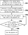
- FIG. 7 is a flow diagram of a memory management method illustrated according to one exemplary embodiment of the invention.
- a first related factor is determined according to a first threshold and a max read error bit of a physical unit.
- a fourth threshold is determined according to a second threshold, a third threshold and the first related factor.
- the physical unit is read according to a reading command, and a read count of the physical unit is updated.
- step S 704 whether the updated read count is not less than the fourth threshold is determined, and the physical unit is scanned (step S 705 ) if the updated read count is not less than the fourth threshold (the determination result in step S 704 is YES).
- Step S 703 may be performed if the updated read count is less than the fourth threshold (the determination result in step S 704 is NO).
- FIG. 8 is a flow diagram of a memory management method illustrated according to one exemplary embodiment of the invention.
- steps S 801 to S 805 for specific contents of steps S 801 to S 805 , reference may be made to the above-mentioned steps S 701 to S 705 . The steps are described above in detail, and descriptions thereof are omitted here.
- step S 803 during the reading of the physical unit, a read error bit of the physical unit is also obtained in addition to updating the read count of the physical unit.
- step S 806 whether the updated read error bit is greater than the first threshold (i.e., a read error bit threshold) is determined.
- the first threshold i.e., a read error bit threshold
- step S 807 The physical unit is refreshed (in step S 807 ) if it is determined that the read error bit is greater than the first threshold (the determination result in step S 806 is YES).
- the updated read count is recorded (in step S 808 ) if it is determined that the read error bit is not greater than the first threshold (the determination result in step S 806 is NO), and step S 803 may be performed.
- step S 809 whether the read error bit is greater than a max read error bit is determined.
- the max read error bit is updated according to the read error bit (in step S 810 ) if it is determined that the read error bit of the physical unit is greater than the max read error bit (the determination result in step S 809 is YES).
- Step S 803 may be performed if it is determined that the read error bit of the physical unit is not greater than the max read error bit (the determination result in step S 809 is NO).
- the memory management circuit 502 stores, for example, all the thresholds, the read counts, the (max) read error bits, calculation results and other data into specific regions of the rewritable non-volatile memory module 406 .
- the memory management method, the memory storage device and the memory control circuit unit provided by the invention take comprehensive consideration of the influence of the erase count and the read error bit on the read count threshold, and can dynamically calculate the read count threshold of each physical unit according to the max read error bit of each physical unit, so as to accurately determine whether the physical unit needs to be subjected to data scanning. Therefore, unnecessary data scanning may be effectively reduced, and/or the problem of data loss caused by untimely scanning of the physical unit may be avoided, and the efficiency of a memory is improved.
Landscapes
- Engineering & Computer Science (AREA)
- Theoretical Computer Science (AREA)
- Physics & Mathematics (AREA)
- General Engineering & Computer Science (AREA)
- General Physics & Mathematics (AREA)
- Human Computer Interaction (AREA)
- Quality & Reliability (AREA)
- Computer Security & Cryptography (AREA)
- Techniques For Improving Reliability Of Storages (AREA)
- Read Only Memory (AREA)
Abstract
Description
thresholdnext=thresholdpre+thresholdnormal×factorerror bit (2)
| TABLE 1 | ||
| Pre-set | ||
| Erase | read count | |
| count | threshold | |
| FULL SLC | 00-50 | 5.0M |
| Erase Count | 51-4000 | 5.0M |
| Group | 4001-10000 | 3.2M |
| 10001-20000 | 2.5M | |
| 20001- | 600k | |
| FULL TLC | 0-50 | 1.0M |
| Erase Count | 51-150 | 2.5M |
| Group | 151-500 | 1.9M |
| 501-1000 | 1.4M | |
| 1001- | 500k | |
| Open SLC | 00-50 | 3.0M |
| Erase Count | 51-4000 | 3.0M |
| Group | 4001-10000 | 2.1M |
| 10001-20000 | 1.6M | |
| 20001- | 400k | |
| Open TLC | 0-50 | 500k |
| Erase Count | 51-150 | 1.4M |
| Group | 151-500 | 1.1M |
| 501-1000 | 800k | |
| 1001- | 250k | |
Claims (21)
Applications Claiming Priority (2)
| Application Number | Priority Date | Filing Date | Title |
|---|---|---|---|
| CN201911310733.4 | 2019-12-18 | ||
| CN201911310733.4A CN111078149B (en) | 2019-12-18 | 2019-12-18 | Memory management method, memory storage device and memory control circuit unit |
Publications (2)
| Publication Number | Publication Date |
|---|---|
| US20210191635A1 US20210191635A1 (en) | 2021-06-24 |
| US11586364B2 true US11586364B2 (en) | 2023-02-21 |
Family
ID=70315668
Family Applications (1)
| Application Number | Title | Priority Date | Filing Date |
|---|---|---|---|
| US16/779,675 Active 2041-04-28 US11586364B2 (en) | 2019-12-18 | 2020-02-03 | Memory management method, memory storage device and memory control circuit unit |
Country Status (2)
| Country | Link |
|---|---|
| US (1) | US11586364B2 (en) |
| CN (1) | CN111078149B (en) |
Families Citing this family (14)
| Publication number | Priority date | Publication date | Assignee | Title |
|---|---|---|---|---|
| US11816043B2 (en) | 2018-06-25 | 2023-11-14 | Alibaba Group Holding Limited | System and method for managing resources of a storage device and quantifying the cost of I/O requests |
| US11061735B2 (en) | 2019-01-02 | 2021-07-13 | Alibaba Group Holding Limited | System and method for offloading computation to storage nodes in distributed system |
| US10860223B1 (en) | 2019-07-18 | 2020-12-08 | Alibaba Group Holding Limited | Method and system for enhancing a distributed storage system by decoupling computation and network tasks |
| US11617282B2 (en) | 2019-10-01 | 2023-03-28 | Alibaba Group Holding Limited | System and method for reshaping power budget of cabinet to facilitate improved deployment density of servers |
| US11449455B2 (en) | 2020-01-15 | 2022-09-20 | Alibaba Group Holding Limited | Method and system for facilitating a high-capacity object storage system with configuration agility and mixed deployment flexibility |
| US11379447B2 (en) | 2020-02-06 | 2022-07-05 | Alibaba Group Holding Limited | Method and system for enhancing IOPS of a hard disk drive system based on storing metadata in host volatile memory and data in non-volatile memory using a shared controller |
| US11449386B2 (en) * | 2020-03-20 | 2022-09-20 | Alibaba Group Holding Limited | Method and system for optimizing persistent memory on data retention, endurance, and performance for host memory |
| US11385833B2 (en) | 2020-04-20 | 2022-07-12 | Alibaba Group Holding Limited | Method and system for facilitating a light-weight garbage collection with a reduced utilization of resources |
| US11507499B2 (en) | 2020-05-19 | 2022-11-22 | Alibaba Group Holding Limited | System and method for facilitating mitigation of read/write amplification in data compression |
| US11556277B2 (en) | 2020-05-19 | 2023-01-17 | Alibaba Group Holding Limited | System and method for facilitating improved performance in ordering key-value storage with input/output stack simplification |
| US11487465B2 (en) | 2020-12-11 | 2022-11-01 | Alibaba Group Holding Limited | Method and system for a local storage engine collaborating with a solid state drive controller |
| US11734115B2 (en) | 2020-12-28 | 2023-08-22 | Alibaba Group Holding Limited | Method and system for facilitating write latency reduction in a queue depth of one scenario |
| US11726699B2 (en) | 2021-03-30 | 2023-08-15 | Alibaba Singapore Holding Private Limited | Method and system for facilitating multi-stream sequential read performance improvement with reduced read amplification |
| CN114327265B (en) * | 2021-12-23 | 2023-05-30 | 群联电子股份有限公司 | Read interference checking method, memory storage device and control circuit unit |
Citations (6)
| Publication number | Priority date | Publication date | Assignee | Title |
|---|---|---|---|---|
| TWI373771B (en) | 2008-06-06 | 2012-10-01 | Phison Electronics Corp | Memory management method for non-volatile memory and controller using the same |
| US20140136883A1 (en) * | 2012-11-15 | 2014-05-15 | Lsi Corporation | Read disturb effect determination |
| US20170075593A1 (en) * | 2015-09-11 | 2017-03-16 | Sandisk Technologies Inc. | System and method for counter flush frequency |
| TWI587304B (en) | 2016-03-09 | 2017-06-11 | 群聯電子股份有限公司 | Memory managing method, memory control circuit unit and mempry storage apparatus |
| US20190130983A1 (en) * | 2017-10-31 | 2019-05-02 | Micron Technology, Inc. | Slc page read |
| US20200210303A1 (en) * | 2019-01-02 | 2020-07-02 | SK Hynix Inc. | Controller and operation method thereof |
Family Cites Families (9)
| Publication number | Priority date | Publication date | Assignee | Title |
|---|---|---|---|---|
| CN101615427B (en) * | 2008-06-24 | 2012-08-08 | 群联电子股份有限公司 | Memory management method of non-volatile memory and controller using the method |
| US20140068378A1 (en) * | 2012-08-31 | 2014-03-06 | Kabushiki Kaisha Toshiba | Semiconductor storage device and memory controller |
| TWI490871B (en) * | 2014-07-11 | 2015-07-01 | Phison Electronics Corp | Method for preventing read-disturb, memory control circuit unit and memory storage apparatus |
| CN105320464B (en) * | 2014-07-21 | 2018-07-31 | 群联电子股份有限公司 | Method for preventing read interference, memory control circuit unit and memory device |
| CN106484308B (en) * | 2015-08-26 | 2019-08-06 | 群联电子股份有限公司 | Data protection method, memory control circuit unit and memory storage device |
| TWI591482B (en) * | 2016-01-30 | 2017-07-11 | 群聯電子股份有限公司 | Data protecting method, memory control circuit unit and memory storage device |
| CN107045890B (en) * | 2016-02-05 | 2020-02-07 | 群联电子股份有限公司 | Data protection method, memory control circuit unit and memory storage device |
| CN107204205B (en) * | 2016-03-16 | 2020-05-26 | 群联电子股份有限公司 | Memory management method, memory control circuit unit and memory storage device |
| CN110333770B (en) * | 2019-07-10 | 2023-05-09 | 合肥兆芯电子有限公司 | Memory management method, memory storage device and memory control circuit unit |
-
2019
- 2019-12-18 CN CN201911310733.4A patent/CN111078149B/en active Active
-
2020
- 2020-02-03 US US16/779,675 patent/US11586364B2/en active Active
Patent Citations (6)
| Publication number | Priority date | Publication date | Assignee | Title |
|---|---|---|---|---|
| TWI373771B (en) | 2008-06-06 | 2012-10-01 | Phison Electronics Corp | Memory management method for non-volatile memory and controller using the same |
| US20140136883A1 (en) * | 2012-11-15 | 2014-05-15 | Lsi Corporation | Read disturb effect determination |
| US20170075593A1 (en) * | 2015-09-11 | 2017-03-16 | Sandisk Technologies Inc. | System and method for counter flush frequency |
| TWI587304B (en) | 2016-03-09 | 2017-06-11 | 群聯電子股份有限公司 | Memory managing method, memory control circuit unit and mempry storage apparatus |
| US20190130983A1 (en) * | 2017-10-31 | 2019-05-02 | Micron Technology, Inc. | Slc page read |
| US20200210303A1 (en) * | 2019-01-02 | 2020-07-02 | SK Hynix Inc. | Controller and operation method thereof |
Non-Patent Citations (1)
| Title |
|---|
| "Office Action of Taiwan Counterpart Application", dated Dec. 29, 2020, p. 1-p. 11. |
Also Published As
| Publication number | Publication date |
|---|---|
| US20210191635A1 (en) | 2021-06-24 |
| CN111078149B (en) | 2023-09-26 |
| CN111078149A (en) | 2020-04-28 |
Similar Documents
| Publication | Publication Date | Title |
|---|---|---|
| US11586364B2 (en) | Memory management method, memory storage device and memory control circuit unit | |
| US11573704B2 (en) | Memory control method, memory storage device and memory control circuit unit | |
| US10782920B2 (en) | Data access method, memory storage apparatus and memory control circuit unit | |
| US10810121B2 (en) | Data merge method for rewritable non-volatile memory storage device and memory control circuit unit | |
| US11797222B2 (en) | Read disturb checking method, memory storage device and memory control circuit unit | |
| US11221791B2 (en) | Memory management method, memory device, and memory control circuit for improving data classification | |
| CN114327265A (en) | Read disturb check method, memory storage device, and control circuit unit | |
| US11301311B2 (en) | Memory control method, memory storage device, and memory control circuit unit | |
| US11010290B2 (en) | Method for reading management information according to updating data reflecting both of host write and data merge, memory storage device and memory control circuit unit | |
| US12124743B2 (en) | Data reading method, memory storage device, and memory control circuit unit | |
| US20240028506A1 (en) | Mapping table re-building method, memory storage device and memory control circuit unit | |
| US11983069B2 (en) | Data rebuilding method, memory storage apparatus, and memory control circuit unit | |
| US11087848B1 (en) | Data arranging method, memory control circuit unit and memory storage device for flash memory for improving the performance of valid data merging operation | |
| US20220164133A1 (en) | Memory control method, memory storage device and memory control circuit unit | |
| US12293792B2 (en) | Voltage prediction method, memory storage device and memory control circuit unit | |
| TWI784224B (en) | Memory management method, memory storage device and memory control circuit unit | |
| US11604586B2 (en) | Data protection method, with disk array tags, memory storage device and memory control circuit unit | |
| US10942680B2 (en) | Data writing method, memory storage device and memory control circuit unit | |
| US10884660B2 (en) | Memory management method, memory storage device and memory control circuit unit | |
| US20220075715A1 (en) | Memory management method, memory storage device and memory control circuit unit | |
| US20210357145A1 (en) | Data writing method, memory storage device and memory control circuit unit | |
| US12148486B2 (en) | Read voltage adjustment method, memory storage device and memory control circuit unit | |
| US12461671B2 (en) | Memory management method for improving the utilization rate, memory storage device, and memory control circuit unit | |
| US20260024598A1 (en) | Wear leveling method, memory storage device and memory control circuit unit | |
| US12561064B2 (en) | Memory management method, memory storage device, and memory control circuit unit |
Legal Events
| Date | Code | Title | Description |
|---|---|---|---|
| AS | Assignment |
Owner name: HEFEI CORE STORAGE ELECTRONIC LIMITED, CHINA Free format text: ASSIGNMENT OF ASSIGNORS INTEREST;ASSIGNORS:HU, XIN;XU, LIANG;ZHANG, XIAOYANG;AND OTHERS;REEL/FRAME:051695/0228 Effective date: 20200131 |
|
| FEPP | Fee payment procedure |
Free format text: ENTITY STATUS SET TO UNDISCOUNTED (ORIGINAL EVENT CODE: BIG.); ENTITY STATUS OF PATENT OWNER: SMALL ENTITY |
|
| STPP | Information on status: patent application and granting procedure in general |
Free format text: DOCKETED NEW CASE - READY FOR EXAMINATION |
|
| STPP | Information on status: patent application and granting procedure in general |
Free format text: NON FINAL ACTION MAILED |
|
| STPP | Information on status: patent application and granting procedure in general |
Free format text: RESPONSE TO NON-FINAL OFFICE ACTION ENTERED AND FORWARDED TO EXAMINER |
|
| STPP | Information on status: patent application and granting procedure in general |
Free format text: FINAL REJECTION MAILED |
|
| STPP | Information on status: patent application and granting procedure in general |
Free format text: RESPONSE AFTER FINAL ACTION FORWARDED TO EXAMINER |
|
| STPP | Information on status: patent application and granting procedure in general |
Free format text: NOTICE OF ALLOWANCE MAILED -- APPLICATION RECEIVED IN OFFICE OF PUBLICATIONS |
|
| FEPP | Fee payment procedure |
Free format text: ENTITY STATUS SET TO SMALL (ORIGINAL EVENT CODE: SMAL); ENTITY STATUS OF PATENT OWNER: SMALL ENTITY |
|
| STCF | Information on status: patent grant |
Free format text: PATENTED CASE |