US11574976B2 - Display device - Google Patents
Display device Download PDFInfo
- Publication number
- US11574976B2 US11574976B2 US17/469,269 US202117469269A US11574976B2 US 11574976 B2 US11574976 B2 US 11574976B2 US 202117469269 A US202117469269 A US 202117469269A US 11574976 B2 US11574976 B2 US 11574976B2
- Authority
- US
- United States
- Prior art keywords
- driving transistor
- display device
- electrode
- voltage
- pixels
- Prior art date
- Legal status (The legal status is an assumption and is not a legal conclusion. Google has not performed a legal analysis and makes no representation as to the accuracy of the status listed.)
- Active
Links
- 239000000758 substrate Substances 0.000 claims abstract description 29
- 239000003990 capacitor Substances 0.000 claims description 36
- 239000010410 layer Substances 0.000 description 96
- 230000015556 catabolic process Effects 0.000 description 8
- 238000006731 degradation reaction Methods 0.000 description 8
- 239000011810 insulating material Substances 0.000 description 8
- 239000010936 titanium Substances 0.000 description 8
- 239000004065 semiconductor Substances 0.000 description 7
- 238000010586 diagram Methods 0.000 description 6
- 239000011347 resin Substances 0.000 description 6
- 229920005989 resin Polymers 0.000 description 6
- RTAQQCXQSZGOHL-UHFFFAOYSA-N Titanium Chemical compound [Ti] RTAQQCXQSZGOHL-UHFFFAOYSA-N 0.000 description 5
- 239000004020 conductor Substances 0.000 description 5
- 229910052719 titanium Inorganic materials 0.000 description 5
- XUIMIQQOPSSXEZ-UHFFFAOYSA-N Silicon Chemical compound [Si] XUIMIQQOPSSXEZ-UHFFFAOYSA-N 0.000 description 4
- 239000011651 chromium Substances 0.000 description 4
- 150000001875 compounds Chemical class 0.000 description 4
- 239000010949 copper Substances 0.000 description 4
- 150000002894 organic compounds Chemical class 0.000 description 4
- 239000002096 quantum dot Substances 0.000 description 4
- 229910052710 silicon Inorganic materials 0.000 description 4
- 239000010703 silicon Substances 0.000 description 4
- 102100031699 Choline transporter-like protein 1 Human genes 0.000 description 3
- 102100035954 Choline transporter-like protein 2 Human genes 0.000 description 3
- 101000940912 Homo sapiens Choline transporter-like protein 1 Proteins 0.000 description 3
- 101000948115 Homo sapiens Choline transporter-like protein 2 Proteins 0.000 description 3
- BQCADISMDOOEFD-UHFFFAOYSA-N Silver Chemical compound [Ag] BQCADISMDOOEFD-UHFFFAOYSA-N 0.000 description 3
- -1 acryl Chemical group 0.000 description 3
- 229910052782 aluminium Inorganic materials 0.000 description 3
- XAGFODPZIPBFFR-UHFFFAOYSA-N aluminium Chemical compound [Al] XAGFODPZIPBFFR-UHFFFAOYSA-N 0.000 description 3
- AMGQUBHHOARCQH-UHFFFAOYSA-N indium;oxotin Chemical compound [In].[Sn]=O AMGQUBHHOARCQH-UHFFFAOYSA-N 0.000 description 3
- BASFCYQUMIYNBI-UHFFFAOYSA-N platinum Chemical compound [Pt] BASFCYQUMIYNBI-UHFFFAOYSA-N 0.000 description 3
- 229910052709 silver Inorganic materials 0.000 description 3
- 239000004332 silver Substances 0.000 description 3
- VYZAMTAEIAYCRO-UHFFFAOYSA-N Chromium Chemical compound [Cr] VYZAMTAEIAYCRO-UHFFFAOYSA-N 0.000 description 2
- RYGMFSIKBFXOCR-UHFFFAOYSA-N Copper Chemical compound [Cu] RYGMFSIKBFXOCR-UHFFFAOYSA-N 0.000 description 2
- 229910052804 chromium Inorganic materials 0.000 description 2
- 229910052802 copper Inorganic materials 0.000 description 2
- 239000011521 glass Substances 0.000 description 2
- 239000010931 gold Substances 0.000 description 2
- 239000011777 magnesium Substances 0.000 description 2
- 239000000463 material Substances 0.000 description 2
- 239000011159 matrix material Substances 0.000 description 2
- 229910052751 metal Inorganic materials 0.000 description 2
- 239000002184 metal Substances 0.000 description 2
- 230000004048 modification Effects 0.000 description 2
- 238000012986 modification Methods 0.000 description 2
- 230000002093 peripheral effect Effects 0.000 description 2
- 239000004033 plastic Substances 0.000 description 2
- 230000003252 repetitive effect Effects 0.000 description 2
- FDRNXKXKFNHNCA-UHFFFAOYSA-N 4-(4-anilinophenyl)-n-phenylaniline Chemical compound C=1C=C(C=2C=CC(NC=3C=CC=CC=3)=CC=2)C=CC=1NC1=CC=CC=C1 FDRNXKXKFNHNCA-UHFFFAOYSA-N 0.000 description 1
- 239000002011 CNT10 Substances 0.000 description 1
- 102100039497 Choline transporter-like protein 3 Human genes 0.000 description 1
- 239000004593 Epoxy Substances 0.000 description 1
- GYHNNYVSQQEPJS-UHFFFAOYSA-N Gallium Chemical compound [Ga] GYHNNYVSQQEPJS-UHFFFAOYSA-N 0.000 description 1
- 101000889279 Homo sapiens Choline transporter-like protein 3 Proteins 0.000 description 1
- 101000685663 Homo sapiens Sodium/nucleoside cotransporter 1 Proteins 0.000 description 1
- 101000821827 Homo sapiens Sodium/nucleoside cotransporter 2 Proteins 0.000 description 1
- 101000822028 Homo sapiens Solute carrier family 28 member 3 Proteins 0.000 description 1
- FYYHWMGAXLPEAU-UHFFFAOYSA-N Magnesium Chemical compound [Mg] FYYHWMGAXLPEAU-UHFFFAOYSA-N 0.000 description 1
- ZOKXTWBITQBERF-UHFFFAOYSA-N Molybdenum Chemical compound [Mo] ZOKXTWBITQBERF-UHFFFAOYSA-N 0.000 description 1
- 229920001609 Poly(3,4-ethylenedioxythiophene) Polymers 0.000 description 1
- 239000004642 Polyimide Substances 0.000 description 1
- 101100328521 Schizosaccharomyces pombe (strain 972 / ATCC 24843) cnt6 gene Proteins 0.000 description 1
- 229910052581 Si3N4 Inorganic materials 0.000 description 1
- VYPSYNLAJGMNEJ-UHFFFAOYSA-N Silicium dioxide Chemical compound O=[Si]=O VYPSYNLAJGMNEJ-UHFFFAOYSA-N 0.000 description 1
- 102100023116 Sodium/nucleoside cotransporter 1 Human genes 0.000 description 1
- 102100021541 Sodium/nucleoside cotransporter 2 Human genes 0.000 description 1
- 102100021470 Solute carrier family 28 member 3 Human genes 0.000 description 1
- ATJFFYVFTNAWJD-UHFFFAOYSA-N Tin Chemical compound [Sn] ATJFFYVFTNAWJD-UHFFFAOYSA-N 0.000 description 1
- 229910045601 alloy Inorganic materials 0.000 description 1
- 239000000956 alloy Substances 0.000 description 1
- 229910021417 amorphous silicon Inorganic materials 0.000 description 1
- QVGXLLKOCUKJST-UHFFFAOYSA-N atomic oxygen Chemical compound [O] QVGXLLKOCUKJST-UHFFFAOYSA-N 0.000 description 1
- 229910052793 cadmium Inorganic materials 0.000 description 1
- BDOSMKKIYDKNTQ-UHFFFAOYSA-N cadmium atom Chemical compound [Cd] BDOSMKKIYDKNTQ-UHFFFAOYSA-N 0.000 description 1
- 239000011258 core-shell material Substances 0.000 description 1
- 230000003247 decreasing effect Effects 0.000 description 1
- KPUWHANPEXNPJT-UHFFFAOYSA-N disiloxane Chemical class [SiH3]O[SiH3] KPUWHANPEXNPJT-UHFFFAOYSA-N 0.000 description 1
- 229910052733 gallium Inorganic materials 0.000 description 1
- 229910052732 germanium Inorganic materials 0.000 description 1
- GNPVGFCGXDBREM-UHFFFAOYSA-N germanium atom Chemical compound [Ge] GNPVGFCGXDBREM-UHFFFAOYSA-N 0.000 description 1
- PCHJSUWPFVWCPO-UHFFFAOYSA-N gold Chemical compound [Au] PCHJSUWPFVWCPO-UHFFFAOYSA-N 0.000 description 1
- 229910052737 gold Inorganic materials 0.000 description 1
- 229910021480 group 4 element Inorganic materials 0.000 description 1
- 229910052735 hafnium Inorganic materials 0.000 description 1
- VBJZVLUMGGDVMO-UHFFFAOYSA-N hafnium atom Chemical compound [Hf] VBJZVLUMGGDVMO-UHFFFAOYSA-N 0.000 description 1
- RBTKNAXYKSUFRK-UHFFFAOYSA-N heliogen blue Chemical compound [Cu].[N-]1C2=C(C=CC=C3)C3=C1N=C([N-]1)C3=CC=CC=C3C1=NC([N-]1)=C(C=CC=C3)C3=C1N=C([N-]1)C3=CC=CC=C3C1=N2 RBTKNAXYKSUFRK-UHFFFAOYSA-N 0.000 description 1
- 229910052738 indium Inorganic materials 0.000 description 1
- APFVFJFRJDLVQX-UHFFFAOYSA-N indium atom Chemical compound [In] APFVFJFRJDLVQX-UHFFFAOYSA-N 0.000 description 1
- 239000004973 liquid crystal related substance Substances 0.000 description 1
- 229910052749 magnesium Inorganic materials 0.000 description 1
- 229910044991 metal oxide Inorganic materials 0.000 description 1
- 150000004706 metal oxides Chemical class 0.000 description 1
- 229910052750 molybdenum Inorganic materials 0.000 description 1
- 239000011733 molybdenum Substances 0.000 description 1
- 150000004767 nitrides Chemical class 0.000 description 1
- 229910052760 oxygen Inorganic materials 0.000 description 1
- 239000001301 oxygen Substances 0.000 description 1
- 230000035515 penetration Effects 0.000 description 1
- 229920002120 photoresistant polymer Polymers 0.000 description 1
- 229910052697 platinum Inorganic materials 0.000 description 1
- 229920002647 polyamide Polymers 0.000 description 1
- 229920000767 polyaniline Polymers 0.000 description 1
- 229910021420 polycrystalline silicon Inorganic materials 0.000 description 1
- 229920002098 polyfluorene Polymers 0.000 description 1
- 229920001721 polyimide Polymers 0.000 description 1
- 239000011241 protective layer Substances 0.000 description 1
- VSZWPYCFIRKVQL-UHFFFAOYSA-N selanylidenegallium;selenium Chemical compound [Se].[Se]=[Ga].[Se]=[Ga] VSZWPYCFIRKVQL-UHFFFAOYSA-N 0.000 description 1
- HQVNEWCFYHHQES-UHFFFAOYSA-N silicon nitride Chemical compound N12[Si]34N5[Si]62N3[Si]51N64 HQVNEWCFYHHQES-UHFFFAOYSA-N 0.000 description 1
- 229910052814 silicon oxide Inorganic materials 0.000 description 1
- 239000000126 substance Substances 0.000 description 1
- JBQYATWDVHIOAR-UHFFFAOYSA-N tellanylidenegermanium Chemical compound [Te]=[Ge] JBQYATWDVHIOAR-UHFFFAOYSA-N 0.000 description 1
- 239000012780 transparent material Substances 0.000 description 1
- TVIVIEFSHFOWTE-UHFFFAOYSA-K tri(quinolin-8-yloxy)alumane Chemical compound [Al+3].C1=CN=C2C([O-])=CC=CC2=C1.C1=CN=C2C([O-])=CC=CC2=C1.C1=CN=C2C([O-])=CC=CC2=C1 TVIVIEFSHFOWTE-UHFFFAOYSA-K 0.000 description 1
- WFKWXMTUELFFGS-UHFFFAOYSA-N tungsten Chemical compound [W] WFKWXMTUELFFGS-UHFFFAOYSA-N 0.000 description 1
- 229910052721 tungsten Inorganic materials 0.000 description 1
- 239000010937 tungsten Substances 0.000 description 1
- LEONUFNNVUYDNQ-UHFFFAOYSA-N vanadium atom Chemical compound [V] LEONUFNNVUYDNQ-UHFFFAOYSA-N 0.000 description 1
Images


Classifications
-
- H—ELECTRICITY
- H01—ELECTRIC ELEMENTS
- H01L—SEMICONDUCTOR DEVICES NOT COVERED BY CLASS H10
- H01L29/00—Semiconductor devices adapted for rectifying, amplifying, oscillating or switching, or capacitors or resistors with at least one potential-jump barrier or surface barrier, e.g. PN junction depletion layer or carrier concentration layer; Details of semiconductor bodies or of electrodes thereof ; Multistep manufacturing processes therefor
- H01L29/66—Types of semiconductor device ; Multistep manufacturing processes therefor
- H01L29/68—Types of semiconductor device ; Multistep manufacturing processes therefor controllable by only the electric current supplied, or only the electric potential applied, to an electrode which does not carry the current to be rectified, amplified or switched
- H01L29/76—Unipolar devices, e.g. field effect transistors
- H01L29/772—Field effect transistors
- H01L29/78—Field effect transistors with field effect produced by an insulated gate
- H01L29/786—Thin film transistors, i.e. transistors with a channel being at least partly a thin film
- H01L29/78606—Thin film transistors, i.e. transistors with a channel being at least partly a thin film with supplementary region or layer in the thin film or in the insulated bulk substrate supporting it for controlling or increasing the safety of the device
- H01L29/78618—Thin film transistors, i.e. transistors with a channel being at least partly a thin film with supplementary region or layer in the thin film or in the insulated bulk substrate supporting it for controlling or increasing the safety of the device characterised by the drain or the source properties, e.g. the doping structure, the composition, the sectional shape or the contact structure
-
- H01L27/3262—
-
- H—ELECTRICITY
- H10—SEMICONDUCTOR DEVICES; ELECTRIC SOLID-STATE DEVICES NOT OTHERWISE PROVIDED FOR
- H10K—ORGANIC ELECTRIC SOLID-STATE DEVICES
- H10K59/00—Integrated devices, or assemblies of multiple devices, comprising at least one organic light-emitting element covered by group H10K50/00
- H10K59/10—OLED displays
- H10K59/12—Active-matrix OLED [AMOLED] displays
- H10K59/131—Interconnections, e.g. wiring lines or terminals
-
- H—ELECTRICITY
- H10—SEMICONDUCTOR DEVICES; ELECTRIC SOLID-STATE DEVICES NOT OTHERWISE PROVIDED FOR
- H10K—ORGANIC ELECTRIC SOLID-STATE DEVICES
- H10K59/00—Integrated devices, or assemblies of multiple devices, comprising at least one organic light-emitting element covered by group H10K50/00
- H10K59/10—OLED displays
- H10K59/12—Active-matrix OLED [AMOLED] displays
- H10K59/122—Pixel-defining structures or layers, e.g. banks
-
- G—PHYSICS
- G09—EDUCATION; CRYPTOGRAPHY; DISPLAY; ADVERTISING; SEALS
- G09G—ARRANGEMENTS OR CIRCUITS FOR CONTROL OF INDICATING DEVICES USING STATIC MEANS TO PRESENT VARIABLE INFORMATION
- G09G3/00—Control arrangements or circuits, of interest only in connection with visual indicators other than cathode-ray tubes
- G09G3/20—Control arrangements or circuits, of interest only in connection with visual indicators other than cathode-ray tubes for presentation of an assembly of a number of characters, e.g. a page, by composing the assembly by combination of individual elements arranged in a matrix no fixed position being assigned to or needed to be assigned to the individual characters or partial characters
- G09G3/22—Control arrangements or circuits, of interest only in connection with visual indicators other than cathode-ray tubes for presentation of an assembly of a number of characters, e.g. a page, by composing the assembly by combination of individual elements arranged in a matrix no fixed position being assigned to or needed to be assigned to the individual characters or partial characters using controlled light sources
- G09G3/30—Control arrangements or circuits, of interest only in connection with visual indicators other than cathode-ray tubes for presentation of an assembly of a number of characters, e.g. a page, by composing the assembly by combination of individual elements arranged in a matrix no fixed position being assigned to or needed to be assigned to the individual characters or partial characters using controlled light sources using electroluminescent panels
- G09G3/32—Control arrangements or circuits, of interest only in connection with visual indicators other than cathode-ray tubes for presentation of an assembly of a number of characters, e.g. a page, by composing the assembly by combination of individual elements arranged in a matrix no fixed position being assigned to or needed to be assigned to the individual characters or partial characters using controlled light sources using electroluminescent panels semiconductive, e.g. using light-emitting diodes [LED]
- G09G3/3208—Control arrangements or circuits, of interest only in connection with visual indicators other than cathode-ray tubes for presentation of an assembly of a number of characters, e.g. a page, by composing the assembly by combination of individual elements arranged in a matrix no fixed position being assigned to or needed to be assigned to the individual characters or partial characters using controlled light sources using electroluminescent panels semiconductive, e.g. using light-emitting diodes [LED] organic, e.g. using organic light-emitting diodes [OLED]
- G09G3/3225—Control arrangements or circuits, of interest only in connection with visual indicators other than cathode-ray tubes for presentation of an assembly of a number of characters, e.g. a page, by composing the assembly by combination of individual elements arranged in a matrix no fixed position being assigned to or needed to be assigned to the individual characters or partial characters using controlled light sources using electroluminescent panels semiconductive, e.g. using light-emitting diodes [LED] organic, e.g. using organic light-emitting diodes [OLED] using an active matrix
- G09G3/3233—Control arrangements or circuits, of interest only in connection with visual indicators other than cathode-ray tubes for presentation of an assembly of a number of characters, e.g. a page, by composing the assembly by combination of individual elements arranged in a matrix no fixed position being assigned to or needed to be assigned to the individual characters or partial characters using controlled light sources using electroluminescent panels semiconductive, e.g. using light-emitting diodes [LED] organic, e.g. using organic light-emitting diodes [OLED] using an active matrix with pixel circuitry controlling the current through the light-emitting element
-
- H—ELECTRICITY
- H01—ELECTRIC ELEMENTS
- H01L—SEMICONDUCTOR DEVICES NOT COVERED BY CLASS H10
- H01L27/00—Devices consisting of a plurality of semiconductor or other solid-state components formed in or on a common substrate
- H01L27/02—Devices consisting of a plurality of semiconductor or other solid-state components formed in or on a common substrate including semiconductor components specially adapted for rectifying, oscillating, amplifying or switching and having at least one potential-jump barrier or surface barrier; including integrated passive circuit elements with at least one potential-jump barrier or surface barrier
- H01L27/12—Devices consisting of a plurality of semiconductor or other solid-state components formed in or on a common substrate including semiconductor components specially adapted for rectifying, oscillating, amplifying or switching and having at least one potential-jump barrier or surface barrier; including integrated passive circuit elements with at least one potential-jump barrier or surface barrier the substrate being other than a semiconductor body, e.g. an insulating body
- H01L27/1214—Devices consisting of a plurality of semiconductor or other solid-state components formed in or on a common substrate including semiconductor components specially adapted for rectifying, oscillating, amplifying or switching and having at least one potential-jump barrier or surface barrier; including integrated passive circuit elements with at least one potential-jump barrier or surface barrier the substrate being other than a semiconductor body, e.g. an insulating body comprising a plurality of TFTs formed on a non-semiconducting substrate, e.g. driving circuits for AMLCDs
- H01L27/124—Devices consisting of a plurality of semiconductor or other solid-state components formed in or on a common substrate including semiconductor components specially adapted for rectifying, oscillating, amplifying or switching and having at least one potential-jump barrier or surface barrier; including integrated passive circuit elements with at least one potential-jump barrier or surface barrier the substrate being other than a semiconductor body, e.g. an insulating body comprising a plurality of TFTs formed on a non-semiconducting substrate, e.g. driving circuits for AMLCDs with a particular composition, shape or layout of the wiring layers specially adapted to the circuit arrangement, e.g. scanning lines in LCD pixel circuits
-
- H01L27/3276—
-
- H—ELECTRICITY
- H10—SEMICONDUCTOR DEVICES; ELECTRIC SOLID-STATE DEVICES NOT OTHERWISE PROVIDED FOR
- H10K—ORGANIC ELECTRIC SOLID-STATE DEVICES
- H10K59/00—Integrated devices, or assemblies of multiple devices, comprising at least one organic light-emitting element covered by group H10K50/00
- H10K59/10—OLED displays
- H10K59/12—Active-matrix OLED [AMOLED] displays
- H10K59/121—Active-matrix OLED [AMOLED] displays characterised by the geometry or disposition of pixel elements
- H10K59/1213—Active-matrix OLED [AMOLED] displays characterised by the geometry or disposition of pixel elements the pixel elements being TFTs
-
- H—ELECTRICITY
- H10—SEMICONDUCTOR DEVICES; ELECTRIC SOLID-STATE DEVICES NOT OTHERWISE PROVIDED FOR
- H10K—ORGANIC ELECTRIC SOLID-STATE DEVICES
- H10K59/00—Integrated devices, or assemblies of multiple devices, comprising at least one organic light-emitting element covered by group H10K50/00
- H10K59/10—OLED displays
- H10K59/12—Active-matrix OLED [AMOLED] displays
- H10K59/121—Active-matrix OLED [AMOLED] displays characterised by the geometry or disposition of pixel elements
- H10K59/1216—Active-matrix OLED [AMOLED] displays characterised by the geometry or disposition of pixel elements the pixel elements being capacitors
-
- H—ELECTRICITY
- H10—SEMICONDUCTOR DEVICES; ELECTRIC SOLID-STATE DEVICES NOT OTHERWISE PROVIDED FOR
- H10K—ORGANIC ELECTRIC SOLID-STATE DEVICES
- H10K59/00—Integrated devices, or assemblies of multiple devices, comprising at least one organic light-emitting element covered by group H10K50/00
- H10K59/10—OLED displays
- H10K59/12—Active-matrix OLED [AMOLED] displays
- H10K59/123—Connection of the pixel electrodes to the thin film transistors [TFT]
-
- H—ELECTRICITY
- H10—SEMICONDUCTOR DEVICES; ELECTRIC SOLID-STATE DEVICES NOT OTHERWISE PROVIDED FOR
- H10K—ORGANIC ELECTRIC SOLID-STATE DEVICES
- H10K59/00—Integrated devices, or assemblies of multiple devices, comprising at least one organic light-emitting element covered by group H10K50/00
- H10K59/10—OLED displays
- H10K59/12—Active-matrix OLED [AMOLED] displays
- H10K59/131—Interconnections, e.g. wiring lines or terminals
- H10K59/1315—Interconnections, e.g. wiring lines or terminals comprising structures specially adapted for lowering the resistance
-
- G—PHYSICS
- G09—EDUCATION; CRYPTOGRAPHY; DISPLAY; ADVERTISING; SEALS
- G09G—ARRANGEMENTS OR CIRCUITS FOR CONTROL OF INDICATING DEVICES USING STATIC MEANS TO PRESENT VARIABLE INFORMATION
- G09G2300/00—Aspects of the constitution of display devices
- G09G2300/04—Structural and physical details of display devices
- G09G2300/0421—Structural details of the set of electrodes
- G09G2300/0426—Layout of electrodes and connections
-
- G—PHYSICS
- G09—EDUCATION; CRYPTOGRAPHY; DISPLAY; ADVERTISING; SEALS
- G09G—ARRANGEMENTS OR CIRCUITS FOR CONTROL OF INDICATING DEVICES USING STATIC MEANS TO PRESENT VARIABLE INFORMATION
- G09G2300/00—Aspects of the constitution of display devices
- G09G2300/04—Structural and physical details of display devices
- G09G2300/0421—Structural details of the set of electrodes
- G09G2300/043—Compensation electrodes or other additional electrodes in matrix displays related to distortions or compensation signals, e.g. for modifying TFT threshold voltage in column driver
-
- G—PHYSICS
- G09—EDUCATION; CRYPTOGRAPHY; DISPLAY; ADVERTISING; SEALS
- G09G—ARRANGEMENTS OR CIRCUITS FOR CONTROL OF INDICATING DEVICES USING STATIC MEANS TO PRESENT VARIABLE INFORMATION
- G09G2300/00—Aspects of the constitution of display devices
- G09G2300/08—Active matrix structure, i.e. with use of active elements, inclusive of non-linear two terminal elements, in the pixels together with light emitting or modulating elements
- G09G2300/0809—Several active elements per pixel in active matrix panels
- G09G2300/0819—Several active elements per pixel in active matrix panels used for counteracting undesired variations, e.g. feedback or autozeroing
-
- G—PHYSICS
- G09—EDUCATION; CRYPTOGRAPHY; DISPLAY; ADVERTISING; SEALS
- G09G—ARRANGEMENTS OR CIRCUITS FOR CONTROL OF INDICATING DEVICES USING STATIC MEANS TO PRESENT VARIABLE INFORMATION
- G09G2300/00—Aspects of the constitution of display devices
- G09G2300/08—Active matrix structure, i.e. with use of active elements, inclusive of non-linear two terminal elements, in the pixels together with light emitting or modulating elements
- G09G2300/0809—Several active elements per pixel in active matrix panels
- G09G2300/0842—Several active elements per pixel in active matrix panels forming a memory circuit, e.g. a dynamic memory with one capacitor
- G09G2300/0861—Several active elements per pixel in active matrix panels forming a memory circuit, e.g. a dynamic memory with one capacitor with additional control of the display period without amending the charge stored in a pixel memory, e.g. by means of additional select electrodes
-
- G—PHYSICS
- G09—EDUCATION; CRYPTOGRAPHY; DISPLAY; ADVERTISING; SEALS
- G09G—ARRANGEMENTS OR CIRCUITS FOR CONTROL OF INDICATING DEVICES USING STATIC MEANS TO PRESENT VARIABLE INFORMATION
- G09G2320/00—Control of display operating conditions
- G09G2320/02—Improving the quality of display appearance
- G09G2320/0233—Improving the luminance or brightness uniformity across the screen
-
- G—PHYSICS
- G09—EDUCATION; CRYPTOGRAPHY; DISPLAY; ADVERTISING; SEALS
- G09G—ARRANGEMENTS OR CIRCUITS FOR CONTROL OF INDICATING DEVICES USING STATIC MEANS TO PRESENT VARIABLE INFORMATION
- G09G2320/00—Control of display operating conditions
- G09G2320/04—Maintaining the quality of display appearance
- G09G2320/043—Preventing or counteracting the effects of ageing
- G09G2320/045—Compensation of drifts in the characteristics of light emitting or modulating elements
-
- G—PHYSICS
- G09—EDUCATION; CRYPTOGRAPHY; DISPLAY; ADVERTISING; SEALS
- G09G—ARRANGEMENTS OR CIRCUITS FOR CONTROL OF INDICATING DEVICES USING STATIC MEANS TO PRESENT VARIABLE INFORMATION
- G09G3/00—Control arrangements or circuits, of interest only in connection with visual indicators other than cathode-ray tubes
- G09G3/20—Control arrangements or circuits, of interest only in connection with visual indicators other than cathode-ray tubes for presentation of an assembly of a number of characters, e.g. a page, by composing the assembly by combination of individual elements arranged in a matrix no fixed position being assigned to or needed to be assigned to the individual characters or partial characters
- G09G3/22—Control arrangements or circuits, of interest only in connection with visual indicators other than cathode-ray tubes for presentation of an assembly of a number of characters, e.g. a page, by composing the assembly by combination of individual elements arranged in a matrix no fixed position being assigned to or needed to be assigned to the individual characters or partial characters using controlled light sources
- G09G3/30—Control arrangements or circuits, of interest only in connection with visual indicators other than cathode-ray tubes for presentation of an assembly of a number of characters, e.g. a page, by composing the assembly by combination of individual elements arranged in a matrix no fixed position being assigned to or needed to be assigned to the individual characters or partial characters using controlled light sources using electroluminescent panels
- G09G3/32—Control arrangements or circuits, of interest only in connection with visual indicators other than cathode-ray tubes for presentation of an assembly of a number of characters, e.g. a page, by composing the assembly by combination of individual elements arranged in a matrix no fixed position being assigned to or needed to be assigned to the individual characters or partial characters using controlled light sources using electroluminescent panels semiconductive, e.g. using light-emitting diodes [LED]
- G09G3/3208—Control arrangements or circuits, of interest only in connection with visual indicators other than cathode-ray tubes for presentation of an assembly of a number of characters, e.g. a page, by composing the assembly by combination of individual elements arranged in a matrix no fixed position being assigned to or needed to be assigned to the individual characters or partial characters using controlled light sources using electroluminescent panels semiconductive, e.g. using light-emitting diodes [LED] organic, e.g. using organic light-emitting diodes [OLED]
- G09G3/3266—Details of drivers for scan electrodes
-
- G—PHYSICS
- G09—EDUCATION; CRYPTOGRAPHY; DISPLAY; ADVERTISING; SEALS
- G09G—ARRANGEMENTS OR CIRCUITS FOR CONTROL OF INDICATING DEVICES USING STATIC MEANS TO PRESENT VARIABLE INFORMATION
- G09G3/00—Control arrangements or circuits, of interest only in connection with visual indicators other than cathode-ray tubes
- G09G3/20—Control arrangements or circuits, of interest only in connection with visual indicators other than cathode-ray tubes for presentation of an assembly of a number of characters, e.g. a page, by composing the assembly by combination of individual elements arranged in a matrix no fixed position being assigned to or needed to be assigned to the individual characters or partial characters
- G09G3/22—Control arrangements or circuits, of interest only in connection with visual indicators other than cathode-ray tubes for presentation of an assembly of a number of characters, e.g. a page, by composing the assembly by combination of individual elements arranged in a matrix no fixed position being assigned to or needed to be assigned to the individual characters or partial characters using controlled light sources
- G09G3/30—Control arrangements or circuits, of interest only in connection with visual indicators other than cathode-ray tubes for presentation of an assembly of a number of characters, e.g. a page, by composing the assembly by combination of individual elements arranged in a matrix no fixed position being assigned to or needed to be assigned to the individual characters or partial characters using controlled light sources using electroluminescent panels
- G09G3/32—Control arrangements or circuits, of interest only in connection with visual indicators other than cathode-ray tubes for presentation of an assembly of a number of characters, e.g. a page, by composing the assembly by combination of individual elements arranged in a matrix no fixed position being assigned to or needed to be assigned to the individual characters or partial characters using controlled light sources using electroluminescent panels semiconductive, e.g. using light-emitting diodes [LED]
- G09G3/3208—Control arrangements or circuits, of interest only in connection with visual indicators other than cathode-ray tubes for presentation of an assembly of a number of characters, e.g. a page, by composing the assembly by combination of individual elements arranged in a matrix no fixed position being assigned to or needed to be assigned to the individual characters or partial characters using controlled light sources using electroluminescent panels semiconductive, e.g. using light-emitting diodes [LED] organic, e.g. using organic light-emitting diodes [OLED]
- G09G3/3275—Details of drivers for data electrodes
-
- H01L27/3265—
Definitions
- Embodiments of the disclosure relate to a display device.
- Flat panel display devices are replacing cathode ray tube display devices as display devices due to their lightweight and thin characteristics.
- As representative examples of such flat panel display devices there are liquid crystal display devices and organic light emitting element display devices.
- Each of pixels included in a display device may include a light emitting element and a driving transistor to drive the light emitting element.
- the driving transistor may be degraded (e.g., by being burned in).
- a driving current provided to the light emitting element may be reduced, so that a luminance of the pixel may be reduced.
- a luminance deviation between the pixels may occur according to a degree of degradation of each of the pixels, so that a display quality of the display device may be decreased.
- Embodiments of the disclosure provide a display device with improved display quality.
- a display device may include a driving transistor disposed on a substrate, a light emitting element disposed on the driving transistor, and a lower electrode disposed between the substrate and the driving transistor.
- the driving transistor may include an active pattern and a gate electrode.
- the active pattern may include a first region, a second region, and a channel region between the first region and the second region.
- the light emitting element may be electrically connected to the second region of the active pattern.
- the lower electrode may overlap the channel region of the active pattern and may provide a back bias voltage to the driving transistor.
- the display device may further include a first power line disposed between the substrate and the driving transistor.
- the first power line may provide a high power voltage to the driving transistor.
- the first power line may overlap the first region of the active pattern and may be electrically connected to the first region of the active pattern.
- the lower electrode and the first power line may be in a same layer.
- the display device may further include a second power line disposed between the substrate and the driving transistor and may provide a low power voltage to the driving transistor.
- the lower electrode and the second power line may be in a same layer.
- the display device may further include a connection pattern electrically connecting the lower electrode and the second power line.
- the back bias voltage may be the low power voltage.
- the low power voltage may be adjusted based on a threshold voltage variation of the driving transistor.
- the display device may further include a first capacitor electrode, the first capacitor electrode and the gate electrode being in a same layer, and a second capacitor electrode disposed on the first capacitor electrode.
- the second capacitor electrode may overlap the first capacitor electrode and may electrically connect the second region of the active pattern and the light emitting element.
- the connection pattern and the second capacitor electrode may be in a same layer.
- the display device may further include a compensation line disposed between the substrate and the driving transistor.
- the compensation line may be electrically connected to the lower electrode and may provide a compensation voltage to the lower electrode.
- the back bias voltage may be the compensation voltage.
- the low compensation voltage may be adjusted based on a threshold voltage variation of the driving transistor.
- the display device may further include a connection pattern electrically connecting the lower electrode and the compensation line.
- the display device may further include a first capacitor electrode, the first capacitor electrode and the gate electrode being in a same layer and a second capacitor electrode disposed on the first capacitor electrode.
- the second capacitor electrode may overlap the first capacitor electrode and may electrically connect the second region of the active pattern and the light emitting element.
- the connection pattern and the second capacitor electrode may be in a same layer.
- the display device may further include a data line disposed between the substrate and the driving transistor.
- the data line may provide a data voltage to the driving transistor.
- the lower electrode and the data line may be in a same layer.
- a display device may include a plurality of pixels, a scan driver, a data driver, a sensing circuit, and a controller.
- Each of the plurality of pixels may include a light emitting element and a driving transistor.
- the driving transistor may generate a driving current to drive the light emitting element.
- the scan driver may provide scan signals to the plurality of pixels.
- the data driver may provide data voltages to the plurality of pixels.
- the sensing circuit may measure a threshold voltage of the driving transistor of each of the plurality of pixels.
- the controller may control the scan driver, the data driver, and the sensing circuit.
- the controller may perform a first compensation for concurrently compensating for the threshold voltage of the driving transistor of each of the plurality of pixels.
- the first compensation may include adjusting a back bias voltage concurrently provided to the driving transistor of each of the plurality of pixels based on a representative value of a measured threshold voltage of the driving transistor of each of the plurality of pixels.
- the controller may perform a second compensation for respectively compensating for the threshold voltage of the driving transistor of each of the plurality of pixels.
- the representative value may be an average value, a maximum value, or a minimum value of the measured threshold voltage of the driving transistor of each of the plurality of pixels.
- the back bias voltage may be a low power voltage.
- the back bias voltage may be a compensation voltage
- the second compensation may include respectively adjusting the data voltages respectively provided to the plurality of pixels based on the measured threshold voltage of the driving transistor of each of the plurality of pixels and adjusted back bias voltage.
- the display device may concurrently compensate for the threshold voltages of the driving transistors for all of the pixels included in the display panel by adjusting the back bias voltage concurrently provided to the driving transistors.
- the display device may respectively compensate for the threshold voltages of the driving transistors for each of the pixels included in the display panel by correcting the data voltage based on a result of the previously performed compensation and the threshold voltage of each of the driving transistors. Therefore, a compensation margin of the threshold voltages of the driving transistors may be improved, so that the display quality of the display device may be improved.
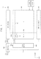
- FIG. 1 is a block diagram schematically illustrating a display device according to embodiments.
- FIG. 2 is an equivalent circuit diagram schematically illustrating a pixel according to an embodiment.
- FIGS. 3 to 9 are layout views schematically illustrating a display panel including the pixel of FIG. 2 .
- FIG. 10 is a schematic cross-sectional view taken along line I-I′ of FIG. 9 .
- FIG. 11 is an equivalent circuit diagram schematically illustrating a pixel according to another embodiment.
- FIG. 12 is a layout view schematically illustrating a display panel including the pixel of FIG. 11 .
- FIG. 13 is a schematic cross-sectional view taken along line II-II′ of FIG. 12 .
- FIG. 1 is a block diagram schematically illustrating a display device according to embodiments.
- a display device 10 may include a display panel 100 , a scan driver 200 , a data driver 300 , a sensing circuit 400 , a power supply, and a controller 500 .
- the display panel 100 may display an image. Pixels PX may be disposed in the display panel 100 .
- the pixels PX may be arranged in a matrix form in a first direction DR 1 and a second direction DR 2 intersecting the first direction DR 1 .
- the second direction DR 2 may be perpendicular to the first direction DR 1 .
- Each of the pixels PX may be electrically connected to a scan line SL, a data line DL, a sensing line SSL, a first power line, and a second power line.
- Each of the pixels PX may receive a voltage and a signal through the above-described lines. As each of the pixels PX emits light based on the voltage and the signal, the image may be displayed on the display panel 100 .
- the scan driver 200 may generate a scan signal based on a first control signal CTL 1 provided from the controller 500 .
- the first control signal CTL 1 may include a vertical start signal, a clock signal, and/or the like.
- the scan signal may include a first scan signal SC and a second scan signal SS.
- the scan signal may be provided to the pixels PX through the scan lines SL.
- the scan driver 200 may be integrated in a peripheral portion of the display panel 100 .
- the scan driver 200 may be implemented with one or more scan integrated circuits (ICs).
- the scan integrated circuits may be mounted directly on the display panel 100 in a chip on glass (COG) manner or a chip on plastic (COP) manner, or may be coupled to the display panel 100 in a chip on film (COF) manner.
- COG chip on glass
- COF chip on film
- the data driver 300 may generate a data voltage DATA based on a second control signal CTL 2 and an output image data ODAT provided from the controller 500 .
- the second control signal CTL 2 may include an output data enable signal, a horizontal start signal, a load signal, and/or the like.
- the data voltage DATA may be provided to the pixels PX through the data lines DL.
- the data driver 300 may be implemented with one or more data ICs.
- the data ICs may be mounted directly on the display panel 100 in the COG manner or the COP manner, or may be coupled to the display panel 100 in the COF manner.
- the sensing circuit 400 may measure threshold voltages of driving transistors (e.g., a driving transistor T 1 of FIG. 2 ) respectively included in the pixels PX based on a third control signal CTL 3 provided from the controller 500 .
- the sensing circuit 400 may measure the threshold voltage of the driving transistor for each of the pixels PX (or each of pixel blocks preset to include at least two pixels PX). Accordingly, a threshold voltage variation indicating a degree of degradation of each of the driving transistors (e.g., a degree of degradation of each of the pixels PX) included in the display panel 100 may be measured for each of the pixels PX (or each of the pixel blocks).
- the sensing circuit 400 may provide an initialization voltage or a reference voltage to the pixels PX. The initialization voltage or the reference voltage may be provided to the pixels PX through the sensing line SSL.
- the data driver 300 and the sensing circuit 400 may be separately configured. In another embodiment, the data driver 300 and the sensing circuit 400 may be integrally configured (or integral with each other).
- the power supply may provide a high power voltage ELVDD and a low power voltage ELVSS to the pixels PX.
- the high power voltage ELVDD may be provided to the pixels PX through the first power line.
- the low power voltage ELVSS may be provided to the pixels PX through the second power line.
- the low power voltage ELVSS may be less than the high power voltage ELVDD.
- the controller 500 may generate the first control signal CTL 1 , the second control signal CTL 2 , and the output image data ODAT based on an input image data IDAT and an input control signal ICTL provided from an external device.
- the input image data IDAT may be RGB data including red image data, green image data, and blue image data.
- the input control signal ICTL may include a master clock signal and an input data enable signal.
- the input control signal ICTL may further include a vertical synchronization signal and a horizontal synchronization signal.
- the controller 500 may calculate a representative value for the display panel 100 based on the threshold voltages of the driving transistors measured for each of the pixels PX by the sensing circuit 400 .
- the representative value may be an average value, a maximum value, or a minimum value of the threshold voltages of the driving transistors included in the display panel 100 .
- the controller 500 may adjust a back bias voltage provided (e.g., applied) to the pixels PX based on a difference between the representative value and a reference threshold voltage.
- the back bias voltage may be concurrently provided to all of the pixels PX included in the display panel 100 .
- the back bias voltage may be provided to each of the driving transistors respectively included in the pixels PX.
- the controller 500 may concurrently compensate for the threshold voltages of the driving transistors for all of the pixels PX included in the display panel 100 (e.g., a first compensation).
- the back bias voltage may be the low power voltage ELVSS.
- the back bias voltage may be a compensation voltage.
- the controller 500 may generate the output image data ODAT based on the input image data IDAT, the representative value (or the adjusted back bias voltage), and the threshold voltages of the driving transistors measured by the sensing circuit 400 .
- the data driver 300 may generate the data voltage DATA based on the output image data ODAT. For example, the degree of degradation of each of the driving transistors and a result of the first compensation performed for all of the pixels PX included in the display panel 100 may be reflected in the generated data voltage DATA. In other words, the threshold voltage variation of each of the driving transistors and a degree of compensation of the threshold voltage of each of the driving transistors compensated for by adjusting the back bias voltage may be reflected in the generated data voltage DATA.
- the data voltages DATA respectively provided to the pixels PX may be different from each other according to the degree of degradation of each of the driving transistors.
- the controller 500 may respectively compensate for the threshold voltages of the driving transistors for each of the pixels PX included in the display panel 100 (e.g., a second compensation).
- FIG. 2 is an equivalent circuit diagram schematically illustrating a pixel according to an embodiment.
- each of the pixel PX may include a pixel circuit PC and a light emitting element EL.
- the pixel circuit PC may provide a driving current to the light emitting element EL.
- the light emitting element EL may emit light based on the driving current provided from the pixel circuit PC.
- the pixel circuit PC may include at least one transistor and at least one capacitor to generate the driving current.
- the pixel circuit PC may include a first transistor T 1 , a second transistor T 2 , a third transistor T 3 , and a storage capacitor CST.
- each of the first to third transistors T 1 , T 2 , and T 3 may be implemented as an N-type transistor or a P-type transistor.
- the first transistor T 1 may include a first gate electrode, a first electrode, and a second electrode.
- the first gate electrode of the first transistor T 1 may be electrically connected to a first node N 1 .
- the first electrode of the first transistor T 1 may be electrically connected to the first power line, and may receive the high power voltage ELVDD.
- the second electrode of the first transistor T 1 may be electrically connected to the second node N 2 .
- the first transistor T 1 may be turned on or off in response to a voltage applied to the first node N 1 . In case that the first transistor T 1 is turned on, the first transistor T 1 may generate the driving current based on the data voltage DATA and the high power voltage ELVDD.
- the driving current may be provided to the light emitting element EL through the second node N 2 , and the light emitting element EL may be driven by the driving current.
- the first transistor T 1 may be referred to as a driving transistor.
- the first transistor T 1 may further include a second gate electrode.
- the second gate electrode of the first transistor T 1 may receive the back bias voltage.
- the back bias voltage may be provided to the first transistor T 1 to compensate for a threshold voltage of the first transistor T 1 .
- the second gate electrode of the first transistor T 1 may be electrically connected to the second power line, and may receive the low power voltage ELVSS.
- the back bias voltage may be the low power voltage ELVSS.
- the second transistor T 2 may include a gate electrode, a first electrode, and a second electrode.
- the gate electrode of the second transistor T 2 may be electrically connected to the scan line SL.
- the first electrode of the second transistor T 2 may be electrically connected to the data line DL and may receive the data voltage DATA.
- the second electrode of the second transistor T 2 may be electrically connected to the first node N 1 .
- the second transistor T 2 may be turned on or off in response to the first scan signal SC. In case that the second transistor T 2 is turned on, the data voltage DATA may be provided to the first node N 1 .
- the second transistor T 2 may be referred to as a switching transistor.
- the third transistor T 3 may include a gate electrode, a first electrode, and a second electrode.
- the gate electrode of the third transistor T 3 may be electrically connected to the scan line SL.
- the first electrode of the third transistor T 3 may be connected to the second node N 2 .
- the second electrode of the third transistor T 3 may be connected to the sensing line SSL.
- the third transistor T 3 may be turned on or off in response to the second scan signal SS. In case that the third transistor T 3 is turned on, the driving current flowing through the second node N 2 may be transferred to the sensing line SSL or the initialization voltage VINT may be provided to the second node N 2 .
- the third transistor T 3 may be referred to as a sensing transistor or an initialization transistor.
- the storage capacitor CST may include a first electrode and a second electrode.
- the first electrode of the storage capacitor CST may be electrically connected to the first node N 1 .
- the second electrode of the storage capacitor CST may be electrically connected to the second node N 2 .
- the storage capacitor CST may store the data voltage DATA provided through the second transistor T 2 .
- the light emitting element EL may include a first electrode and a second electrode.
- the first electrode of the light emitting element EL may be connected to the second node N 2 .
- the second electrode of the light emitting element EL may be connected to the second power line, and may receive the low power voltage ELVSS.
- the first electrode of the light emitting element EL may be an anode electrode
- the second electrode of the light emitting element EL may be a cathode electrode.
- FIGS. 3 to 9 are layout views schematically illustrating a display panel including the pixel of FIG. 2 .
- FIG. 10 is a schematic cross-sectional view taken along line I-I′ of FIG. 9 .
- FIGS. 3 to 9 may correspond to the pixel circuit PC of FIG. 2 .
- a pixel PX is illustrated in FIGS. 3 to 9 , the pixels PX may be arranged in the matrix form in the first direction DR 1 and the second direction DR 2 in the display panel 100 .
- the display panel 100 may include a substrate SUB, a first conductive layer 110 , an active layer 120 , a second conductive layer 130 , a third conductive layer 140 , and the light emitting element EL.
- the light emitting element EL may include a pixel electrode 150 , an emission layer 160 , and a common electrode 170 .
- the substrate SUB may be an insulating substrate formed of a transparent or non-transparent material.
- the substrate SUB may include glass.
- the display panel 100 may be a rigid display panel.
- the substrate SUB may include plastic.
- the display panel 100 may be a flexible display panel.
- the first conductive layer 110 may be disposed on the substrate SUB.
- the first conductive layer 110 may include a conductive material.
- the first conductive layer 110 may include a metal, an alloy, a conductive metal nitride, a conductive metal oxide, a doped oxide semiconductor, a doped silicon semiconductor, and/or the like.
- the first conductive layer 110 may include a first power line 112 , a second power line 111 , a first electrode 113 , first to third data lines 114 a , 114 b , and 114 c , and a sensing line 115 .
- the first power line 112 , the second power line 111 , the first to third data lines 114 a , 114 b , and 114 c , and the sensing line 115 may respectively correspond to the first power line, the second power line, the data line DL, and the sensing line SSL described above with reference to FIG. 1 .
- each of the first power line 112 , the second power line 111 , the first to third data lines 114 a , 114 b , and 114 c , and the sensing line 115 may extend in the second direction DR 2 , and may be spaced apart from each other in the first direction DR 1 .
- the first electrode 113 may be disposed between the first power line 112 and the first to third data lines 114 a , 114 b , and 114 c .
- the first power line 112 may be disposed between the second power line 111 and the first electrode 113 .
- the second power line 111 may be disposed between the first power line 112 and the first electrode 113 .
- a buffer layer may be disposed between the substrate SUB and the first conductive layer 110 .
- the buffer layer may prevent or reduce penetration of foreign substances such as oxygen or moisture through the substrate SUB to an upper portion of the substrate SUB.
- the buffer layer may provide a flat upper surface on the substrate SUB.
- the buffer layer may include an inorganic insulating material such as silicon oxide, silicon nitride, and/or silicon oxynitride. In another embodiment, the buffer layer may be omitted.
- the active layer 120 may be disposed on the first conductive layer 110 .
- the active layer 120 may include an oxide semiconductor, a silicon semiconductor, or the like.
- the oxide semiconductor may include at least one oxide of indium (In), gallium (Ga), tin (Sn), zirconium (Zr), vanadium (V), hafnium (Hf), cadmium (Cd), germanium (Ge), chromium (Cr), titanium (Ti), and zinc (Zn).
- the silicon semiconductor may include amorphous silicon, polycrystalline silicon, or the like.
- a first insulating layer IL 1 may be disposed between the first conductive layer 110 and the active layer 120 .
- the first insulating layer IL 1 may include an inorganic insulating material.
- the active layer 120 may include a first active pattern 121 , a second active pattern 122 , and a third active pattern 123 .
- the first active pattern 121 may be a channel of the first transistor T 1
- the second active pattern 122 may be a channel of the second transistor T 2
- the third active pattern 123 may be a channel of the third transistor T 3 .
- Each of the first to third active patterns 121 , 122 , and 123 may include a first region, a second region, and a channel region between the first region and the second region.
- the first active pattern 121 may include a first region 121 a , a second region 121 b , and a channel region 121 c between the first region 121 a and the second region 121 b .
- the first region 121 a of the first active pattern 121 may overlap the first power line 112 .
- the first region 121 a of the first active pattern 121 may be electrically connected to the first power line 112 through a first contact hole CNT 1 .
- the first transistor T 1 may be electrically connected to the first power line 112 , and may receive the high power voltage ELVDD through the first power line 112 .
- the channel region 121 c of the first active pattern 121 may overlap the first electrode 113 .
- the back bias voltage e.g., the low power voltage ELVSS
- ELVSS low power voltage
- the second conductive layer 130 may be disposed on the active layer 120 .
- the second conductive layer 130 may include a conductive material.
- the second conductive layer 130 may include molybdenum (Mo), copper (Cu), and/or the like.
- a second insulating layer IL 2 may be disposed between the active layer 120 and the second conductive layer 130 .
- the second insulating layer IL 2 may include an inorganic insulating material.
- the second conductive layer 130 may include a scan line 131 and a second electrode 132 .
- the scan line 131 may correspond to the scan line SL described above with reference to FIG. 1 .
- the scan line 131 may extend in the first direction DR 1 , and may include a protrusion protruding in the second direction DR 2 .
- the second active pattern 122 and a portion of the protrusion overlapping the second active pattern 122 may form the second transistor T 2 .
- the third active pattern 123 and a portion of the protrusion overlapping the third active pattern 123 may form the third transistor T 3 .
- the second electrode 132 may be disposed on the first electrode 113 and the first active pattern 121 , and may overlap the first electrode 113 .
- the second electrode 132 may include a first portion 132 a and a second portion 132 b .
- the first portion 132 a may overlap the first active pattern 121 (e.g., the channel region 121 c of the first active pattern 121 ) in a plan view.
- the second portion 132 b may be spaced apart from (e.g., may not overlap) the first active pattern 121 in a plan view.
- the first active pattern 121 and the first portion 132 a of the second electrode 132 overlapping the first active pattern 121 may form the first transistor T 1 .
- the first electrode 113 may be disposed under the first transistor T 1 .
- the first electrode 113 may be disposed between the substrate SUB and the first transistor T 1 .
- the first electrode 113 may be referred to as a lower electrode.
- the first electrode 113 may correspond to the second gate electrode of the first transistor T 1 .
- the back bias voltage e.g., the low power voltage ELVSS
- ELVSS low power voltage
- the first power line 112 , the second power line 111 , the first to third data lines 114 a , 114 b , and 114 c , and the sensing line 115 may disposed under the first transistor T 1 .
- the first power line 112 , the second power line 111 , the first to third data lines 114 a , 114 b , and 114 c , and the sensing line 115 may be disposed between the substrate SUB and the first transistor T 1 .
- the third conductive layer 140 may be disposed on the second conductive layer 130 .
- the third conductive layer 140 may include a conductive material.
- the third conductive layer 140 may include aluminum (Al), titanium (Ti), copper (Cu), and/or the like.
- the third conductive layer 140 may have a multi-layered structure in which a titanium layer, an aluminum layer, and a titanium layer are stacked.
- a third insulating layer IL 3 may be disposed between the second conductive layer 130 and the third conductive layer 140 .
- the third insulating layer IL 3 may include an inorganic insulating material.
- the third conductive layer 140 may include a third electrode 141 , a first connection pattern 142 , a second connection pattern 143 , a third connection pattern 144 , and a fourth connection pattern 145 .
- the third electrode 141 may be disposed on the second electrode 132 .
- the third electrode 141 may overlap the second portion 132 b of the second electrode 132 in a plan view, and may be spaced apart from (e.g., may not overlap) the first portion 132 a of the second electrode 132 .
- the second portion 132 b of the second electrode 132 and a portion of the third electrode 141 overlapping the second portion 132 b may form the storage capacitor CST.
- the second portion 132 b of the second electrode 132 may be referred to as a first capacitor electrode.
- the portion of the third electrode 141 overlapping the second portion 132 b of the second electrode 132 may be referred to as a second capacitor electrode.
- Another portion of the third electrode 141 may be spaced apart from (e.g., may not overlap) the second electrode 132 in a plan view, and may overlap the second region 121 b of the first active pattern 121 .
- the another portion of the third electrode 141 may be electrically connected to the second region 121 b of the first active pattern 121 through a second contact hole CNT 2 .
- the first connection pattern 142 may extend in the first direction DR 1 .
- a first end portion of the first connection pattern 142 may overlap the second power line 111
- a second end portion of the first connection pattern 142 may overlap the first electrode 113 .
- the first end portion of the first connection pattern 142 may be electrically connected to the second power line 111 through a third contact hole CNT 3 .
- the second end portion of the first connection pattern 142 may be electrically connected to the first electrode 113 through a fourth contact hole CNT 4 .
- the first electrode 113 and the second power line 111 may be electrically connected by the first connection pattern 142 .
- the low power voltage ELVSS may be provided to the first electrode 113 through the first connection pattern 142 .
- the low power voltage ELVSS may be provided to the first transistor T 1 as the back bias voltage.
- the back bias voltage may be adjusted based on the difference between the representative value and the reference threshold voltage.
- the back bias voltage may be adjusted based on the average value (or, the minimum value or the maximum value) of the threshold voltage variations of the first transistors T 1 included in the display panel 100 (i.e., the driving transistors T 1 respectively included in the pixels PX).
- the low power voltage ELVSS may be adjusted based on the average value of the threshold voltage variations of the first transistors T 1 included in the display panel 100 .
- the second connection pattern 143 may be electrically connected to the second electrode 132 through a fifth contact hole CNT 5 , and may be electrically connected to the second active pattern 122 through a sixth contact hole CNT 6 .
- the third connection pattern 144 may be electrically connected to the second active pattern 122 through a seventh contact hole CNT 7 , and may be electrically connected to the first data line 114 a through an eighth contact hole CNT 8 .
- the fourth connection pattern 145 may be electrically connected to the sensing line 115 through a ninth contact hole CNT 9 , and may be electrically connected to the third active pattern 123 through a tenth contact hole CNT 10 .
- the third electrode 141 may be electrically connected to the third active pattern 123 through an eleventh contact hole CNT 11 , and may be electrically connected to the first electrode 113 through a twelfth contact hole CNT 12 . As described later, the third electrode 141 may be electrically connected to the pixel electrode 150 included in the light emitting element EL. As the first electrode 113 overlapping the channel region 121 c of the first active pattern 121 is electrically connected to the pixel electrode 150 through the third electrode 141 , a current variation rate may be reduced in a saturation region of a voltage-current characteristic graph of the first transistor T 1 , so that a range of a region where an output current of the first transistor T 1 is constant may be increased.
- the output current of the first transistor T 1 may be maintained to be constant, so that an output saturation characteristic may be improved. Accordingly, a luminance deviation between the pixels PX due to the output current of the first transistor T 1 may be reduced, so that a display quality of the display device 10 may be improved.
- the pixel electrode 150 may be disposed on the third conductive layer 140 .
- the pixel electrode 150 may include a conductive material.
- the pixel electrode 150 may include silver (Ag), indium tin oxide (ITO), and/or the like.
- the pixel electrode 150 may have a multi-layered structure in which an indium tin oxide layer, a silver layer, and an indium tin oxide layer are stacked.
- a fourth insulating layer IL 4 may be disposed between the third conductive layer 140 and the pixel electrode 150 .
- the fourth insulating layer IL 4 may include an inorganic insulating material and/or an organic insulating material.
- the organic insulating material may include a photoresist, a polyacryl-based resin, a polyimide-based resin, a polyamide-based resin, a siloxane-based resin, an acryl-based resin, an epoxy-based resin, and/or the like.
- the pixel electrode 150 may be electrically connected to the third electrode 141 through a contact hole. Accordingly, the pixel electrode 150 may be electrically connected to the first transistor T 1 through the third electrode 141 .
- a fifth insulating layer IL 5 may be disposed on the pixel electrode 150 .
- the fifth insulating layer IL 5 may partially cover (or overlap) the pixel electrode 150 , and may be disposed on the fourth insulating layer IL 4 .
- the fifth insulating layer IL 5 may have a pixel opening exposing at least a portion of the pixel electrode 150 .
- the pixel opening may expose a central portion of the pixel electrode 150
- the fifth insulating layer IL 5 may cover a peripheral portion of the pixel electrode 150 .
- the fifth insulating layer IL 5 may include an organic insulating material.
- the emission layer 160 may be disposed on the pixel electrode 150 .
- the emission layer 160 may be disposed on the pixel electrode 150 exposed by the pixel opening.
- the emission layer 160 may include at least one of an organic light emitting material and a quantum dot.
- the organic light emitting material may include a low molecular organic compound or a high molecular organic compound.
- the low molecular organic compound may include copper phthalocyanine, N,N′-diphenylbenzidine, tris-(8-hydroxyquinoline)aluminum, and/or the like.
- the high molecular organic compound may include poly(3,4-ethylenedioxythiophene), polyaniline, poly-phenylenevinylene, polyfluorene, and/or the like.
- the quantum dot may include a core including a Group II-VI compound, a Group III-V compound, a Group IV-VI compound, a Group IV element, and/or a Group IV compound.
- the quantum dot may have a core-shell structure including the core and a shell surrounding the core. The shell may serve (or function) as a protective layer for preventing the core from being chemically denatured to maintain semiconductor characteristics, and may serve as a charging layer for imparting electrophoretic characteristics to the quantum dot.
- the common electrode 170 may be disposed on the emission layer 160 . In an embodiment, the common electrode 170 may also be disposed on the fifth insulating layer IL 5 .
- the common electrode 170 may include a conductive material.
- the common electrode 170 may include aluminum (Al), platinum (Pt), silver (Ag), magnesium (Mg), gold (Au), chromium (Cr), tungsten (W), titanium (Ti), and/or the like.
- the pixel electrode 150 , the emission layer 160 , and the common electrode 170 may form the light emitting element EL.
- the common electrode 170 may be electrically connected to the second power line 111 .
- the light emitting element EL may receive the low power voltage ELVSS through the second power line 111 .
- FIG. 11 is an equivalent circuit diagram schematically illustrating a pixel according to another embodiment.
- FIG. 12 is a layout view schematically illustrating a display panel including the pixel of FIG. 11 .
- FIG. 13 is a schematic cross-sectional view taken along the line II-II′ of FIG. 12 .
- FIG. 12 may correspond to a pixel circuit PC′ of FIG. 11 .
- a display panel 101 according to another embodiment described with reference to FIGS. 11 to 13 may be substantially identical or similar to the display panel 100 described with reference to FIGS. 2 to 10 but may be different therefrom at least in a compensation line 116 and a first connection pattern 1142 . Therefore, repetitive descriptions will be omitted or simplified.
- each of pixels PX′ may include a pixel circuit PC′ and a light emitting element EL.
- the pixel circuit PC′ may include a first transistor T 1 , a second transistor T 2 , a third transistor T 3 , and a storage capacitor CST.
- the pixel PX′ according to another embodiment described with reference to FIG. 11 may be substantially identical or similar to the pixel PX described with reference to FIG. 2 but may be different therefrom at least in a second gate electrode of the first transistor T 1 . Therefore, repetitive descriptions will be omitted or simplified.
- the first transistor T 1 may include a first gate electrode, a second gate electrode, a first electrode, and a second electrode.
- the second gate electrode of the first transistor T 1 may receive the back bias voltage.
- the back bias voltage may be provided to the first transistor T 1 to compensate for a threshold voltage of the first transistor T 1 .
- the second gate electrode of the first transistor T 1 may be electrically connected to a compensation line, and may receive a compensation voltage CPV.
- the back bias voltage may be the compensation voltage CPV.
- the compensation voltage CPV may be provided separately from the high power voltage ELVDD and the low power voltage ELVSS to the second gate electrode of the first transistor T 1 through the compensation line.
- a display panel 101 may include a substrate SUB, a first conductive layer, an active layer, a second conductive layer, a third conductive layer, and the light emitting element EL.
- the light emitting element EL may include a pixel electrode 150 , an emission layer 160 , and a common electrode 170 .
- the first conductive layer may be disposed on the substrate SUB.
- the active layer may be disposed on the first conductive layer.
- a first insulating layer IL 1 may be disposed between the first conductive layer and the active layer.
- the second conductive layer may be disposed on the active layer.
- a second insulating layer IL 2 may be disposed between the active layer and the second conductive layer.
- the third conductive layer may be disposed on the second conductive layer.
- a third insulating layer IL 3 may be disposed between the second conductive layer and the third conductive layer.
- the light emitting element EL may be disposed on the third conductive layer.
- the first conductive layer may include a first power line 112 , a second power line 111 , a first electrode 113 , first to third data lines 114 a , 114 b , and 114 c , a sensing line 115 , and a compensation line 116 .
- the compensation line 116 may be disposed under the first transistor T 1 .
- the compensation line 116 may be disposed between the substrate SUB and the first transistor T 1 .
- the compensation line 116 may extend in the second direction DR 2 .
- the compensation line 116 may be disposed between the first power line 112 and the second power line 111 .
- the compensation line 116 may be disposed between the first electrode 113 and the first power line 112 .
- the compensation line 116 may be spaced apart from the first power line 112 with the second power line 111 interposed therebetween.
- the compensation line 116 may be spaced apart from the first power line 112 with the first electrode 113 interposed therebetween.
- the compensation line 116 may receive the compensation voltage CPV from the power supply.
- the third conductive layer may include a third electrode 141 , a first connection pattern 1142 , a second connection pattern 143 , a third connection pattern 144 , and a fourth connection pattern 145 .
- the first connection pattern 1142 may extend in the first direction DR 1 .
- a first end portion of the first connection pattern 1142 may overlap the compensation line 116
- a second end portion of the first connection pattern 1142 may overlap the first electrode 113 .
- the first end portion of the first connection pattern 1142 may be electrically connected to the compensation line 116 through a thirteenth contact hole CNT 13 .
- the second end portion of the first connection pattern 1142 may be electrically connected to the first electrode 113 through a fourth contact hole CNT 4 .
- the first electrode 113 and the compensation line 116 may be electrically connected by the first connection pattern 1142 .
- the compensation voltage CPV may be provided to the first electrode 113 through the first connection pattern 1142 .
- the compensation voltage CPV may be provided to the first transistor T 1 as the back bias voltage.
- the back bias voltage may be adjusted based on the difference between the representative value and the reference threshold voltage.
- the back bias voltage may be adjusted based on the average value (or, the minimum value or the maximum value) of the threshold voltage variations of the first transistors T 1 included in the display panel 100 (i.e., the driving transistors T 1 respectively included in the pixels PX′).
- the compensation voltage CPV may be adjusted based on the average value of the threshold voltage variations of the first transistors T 1 included in the display panel 100 .
- a sensing circuit may measure threshold voltages of driving transistors respectively included in pixels.
- a controller may generate corrected output image data reflecting a threshold voltage variation of each of the driving transistors.
- the display device may only respectively compensate for the threshold voltages of the driving transistors for each of the pixels included in a display panel. In this case of such a threshold voltage compensation for each of the pixels, there is a limit of a compensation margin (e.g., about 2V).
- the sensing circuit 400 may measure the threshold voltages of the driving transistors T 1 for each of the pixels PX.
- the controller 500 may adjust the back bias voltage (e.g., the low power voltage ELVSS or the compensation voltage CPV) concurrently provided to the driving transistors T 1 based on the representative value (e.g., the average value, the maximum value, or the minimum value) of the measured threshold voltages of the driving transistors T 1 .
- the controller 500 may perform the first compensation for concurrently compensating for the threshold voltages of the driving transistors T 1 for all of the pixels PX included in the display panel 100 .
- the controller 500 may generate the output image data ODAT reflecting the measured threshold voltages of the driving transistors T 1 and a result of the first compensation (e.g., the adjusted back bias voltage).
- the data voltage DATA may be corrected, so that the degree of degradation of each of the driving transistors T 1 (e.g., the degree of degradation of each of the pixels PX) may be individually reflected.
- the controller 500 may perform the second compensation for respectively compensating the threshold voltage of the driving transistor T 1 for each of the pixels PX included in the display panel 100 . Therefore, a compensation margin of the threshold voltages of the driving transistors T 1 may be improved. Accordingly, the luminance deviation between the pixels PX may be reduced, so that the display quality of the display device 10 may be improved.
Abstract
Description
Claims (20)
Applications Claiming Priority (2)
| Application Number | Priority Date | Filing Date | Title |
|---|---|---|---|
| KR10-2021-0000569 | 2021-01-04 | ||
| KR1020210000569A KR20220099172A (en) | 2021-01-04 | 2021-01-04 | Display device |
Publications (2)
| Publication Number | Publication Date |
|---|---|
| US20220216284A1 US20220216284A1 (en) | 2022-07-07 |
| US11574976B2 true US11574976B2 (en) | 2023-02-07 |
Family
ID=82219036
Family Applications (1)
| Application Number | Title | Priority Date | Filing Date |
|---|---|---|---|
| US17/469,269 Active US11574976B2 (en) | 2021-01-04 | 2021-09-08 | Display device |
Country Status (3)
| Country | Link |
|---|---|
| US (1) | US11574976B2 (en) |
| KR (1) | KR20220099172A (en) |
| CN (1) | CN114725160A (en) |
Citations (8)
| Publication number | Priority date | Publication date | Assignee | Title |
|---|---|---|---|---|
| US20160042694A1 (en) * | 2014-08-07 | 2016-02-11 | Samsung Display Co., Ltd. | Pixel circuit and organic light-emitting diode display including the same |
| KR20170027349A (en) | 2015-09-01 | 2017-03-10 | 엘지디스플레이 주식회사 | Organic light emitting display device |
| US20180061908A1 (en) * | 2016-08-31 | 2018-03-01 | Lg Display Co., Ltd. | Display device |
| KR20180024909A (en) | 2016-08-31 | 2018-03-08 | 엘지디스플레이 주식회사 | driving transistor and Organic light emitting diode display device having the driving transistor, and Method for manufacturing the same |
| KR101954934B1 (en) | 2011-08-08 | 2019-03-07 | 삼성디스플레이 주식회사 | Display device and driving method thereof |
| US20190172881A1 (en) * | 2017-12-06 | 2019-06-06 | Lg Display Co., Ltd. | Organic light emitting display device |
| US20200005708A1 (en) * | 2018-06-28 | 2020-01-02 | Samsung Display Co., Ltd. | Organic light emitting diode display device |
| KR20200075955A (en) | 2018-12-18 | 2020-06-29 | 삼성디스플레이 주식회사 | Pixel circuit and organic light-emitting display device including the same |
-
2021
- 2021-01-04 KR KR1020210000569A patent/KR20220099172A/en active Search and Examination
- 2021-09-08 US US17/469,269 patent/US11574976B2/en active Active
- 2021-10-09 CN CN202111173915.9A patent/CN114725160A/en active Pending
Patent Citations (8)
| Publication number | Priority date | Publication date | Assignee | Title |
|---|---|---|---|---|
| KR101954934B1 (en) | 2011-08-08 | 2019-03-07 | 삼성디스플레이 주식회사 | Display device and driving method thereof |
| US20160042694A1 (en) * | 2014-08-07 | 2016-02-11 | Samsung Display Co., Ltd. | Pixel circuit and organic light-emitting diode display including the same |
| KR20170027349A (en) | 2015-09-01 | 2017-03-10 | 엘지디스플레이 주식회사 | Organic light emitting display device |
| US20180061908A1 (en) * | 2016-08-31 | 2018-03-01 | Lg Display Co., Ltd. | Display device |
| KR20180024909A (en) | 2016-08-31 | 2018-03-08 | 엘지디스플레이 주식회사 | driving transistor and Organic light emitting diode display device having the driving transistor, and Method for manufacturing the same |
| US20190172881A1 (en) * | 2017-12-06 | 2019-06-06 | Lg Display Co., Ltd. | Organic light emitting display device |
| US20200005708A1 (en) * | 2018-06-28 | 2020-01-02 | Samsung Display Co., Ltd. | Organic light emitting diode display device |
| KR20200075955A (en) | 2018-12-18 | 2020-06-29 | 삼성디스플레이 주식회사 | Pixel circuit and organic light-emitting display device including the same |
Also Published As
| Publication number | Publication date |
|---|---|
| KR20220099172A (en) | 2022-07-13 |
| CN114725160A (en) | 2022-07-08 |
| US20220216284A1 (en) | 2022-07-07 |
Similar Documents
| Publication | Publication Date | Title |
|---|---|---|
| US10600368B2 (en) | Organic light-emitting display device | |
| US10971067B1 (en) | AMOLED pixel driving circuit, driving method and terminal | |
| US10475377B2 (en) | Display device and method of driving the same | |
| JP4150012B2 (en) | Organic electroluminescence display panel | |
| KR102642869B1 (en) | Display device | |
| US11335757B2 (en) | Organic light emitting display device | |
| US11881172B2 (en) | Pixel circuit and display device including the same | |
| JP5057731B2 (en) | Display device, module, and electronic device | |
| US11749213B2 (en) | Organic light emitting display device | |
| US20200294449A1 (en) | Pixel array substrate and driving method thereof, display panel, and display device | |
| US10950822B2 (en) | Display device capable of improving light extraction efficiency | |
| US10223972B1 (en) | OLED pixel driving circuit and OLED display device | |
| US20230065100A1 (en) | Display device | |
| US20220085137A1 (en) | Display device | |
| US11133364B2 (en) | Light emitting diode display device | |
| US11574976B2 (en) | Display device | |
| US20230206858A1 (en) | Display Device | |
| WO2021064954A1 (en) | Display device | |
| CN111477174A (en) | Pixel circuit, driving method thereof and display substrate | |
| US20230131089A1 (en) | Display device | |
| CN114097021B (en) | Display panel, driving method thereof and display device | |
| US20220262881A1 (en) | Display device | |
| US20230171997A1 (en) | Display panel with a repair circuit | |
| US20220208931A1 (en) | Foldable display device | |
| US20230337485A1 (en) | Display device |
Legal Events
| Date | Code | Title | Description |
|---|---|---|---|
| AS | Assignment |
Owner name: SAMSUNG DISPLAY CO., LTD., KOREA, REPUBLIC OF Free format text: ASSIGNMENT OF ASSIGNORS INTEREST;ASSIGNORS:JEON, YOUNGJAE;LEE, WOOGEUN;KIM, JONG-IN;AND OTHERS;REEL/FRAME:057437/0865 Effective date: 20210705 |
|
| FEPP | Fee payment procedure |
Free format text: ENTITY STATUS SET TO UNDISCOUNTED (ORIGINAL EVENT CODE: BIG.); ENTITY STATUS OF PATENT OWNER: LARGE ENTITY |
|
| STPP | Information on status: patent application and granting procedure in general |
Free format text: NON FINAL ACTION MAILED |
|
| STPP | Information on status: patent application and granting procedure in general |
Free format text: RESPONSE TO NON-FINAL OFFICE ACTION ENTERED AND FORWARDED TO EXAMINER |
|
| STPP | Information on status: patent application and granting procedure in general |
Free format text: NOTICE OF ALLOWANCE MAILED -- APPLICATION RECEIVED IN OFFICE OF PUBLICATIONS |
|
| STPP | Information on status: patent application and granting procedure in general |
Free format text: PUBLICATIONS -- ISSUE FEE PAYMENT VERIFIED |
|
| STCF | Information on status: patent grant |
Free format text: PATENTED CASE |