US11573356B2 - Diffraction grating comprising double-materials structures - Google Patents
Diffraction grating comprising double-materials structures Download PDFInfo
- Publication number
- US11573356B2 US11573356B2 US16/980,307 US201916980307A US11573356B2 US 11573356 B2 US11573356 B2 US 11573356B2 US 201916980307 A US201916980307 A US 201916980307A US 11573356 B2 US11573356 B2 US 11573356B2
- Authority
- US
- United States
- Prior art keywords
- diffraction grating
- axis
- block
- dielectric material
- grating
- Prior art date
- Legal status (The legal status is an assumption and is not a legal conclusion. Google has not performed a legal analysis and makes no representation as to the accuracy of the status listed.)
- Active
Links
Images


Classifications
-
- G—PHYSICS
- G02—OPTICS
- G02B—OPTICAL ELEMENTS, SYSTEMS OR APPARATUS
- G02B5/00—Optical elements other than lenses
- G02B5/18—Diffraction gratings
- G02B5/1809—Diffraction gratings with pitch less than or comparable to the wavelength
-
- G—PHYSICS
- G02—OPTICS
- G02B—OPTICAL ELEMENTS, SYSTEMS OR APPARATUS
- G02B27/00—Optical systems or apparatus not provided for by any of the groups G02B1/00 - G02B26/00, G02B30/00
- G02B27/42—Diffraction optics, i.e. systems including a diffractive element being designed for providing a diffractive effect
- G02B27/4233—Diffraction optics, i.e. systems including a diffractive element being designed for providing a diffractive effect having a diffractive element [DOE] contributing to a non-imaging application
- G02B27/4244—Diffraction optics, i.e. systems including a diffractive element being designed for providing a diffractive effect having a diffractive element [DOE] contributing to a non-imaging application in wavelength selecting devices
-
- B—PERFORMING OPERATIONS; TRANSPORTING
- B82—NANOTECHNOLOGY
- B82Y—SPECIFIC USES OR APPLICATIONS OF NANOSTRUCTURES; MEASUREMENT OR ANALYSIS OF NANOSTRUCTURES; MANUFACTURE OR TREATMENT OF NANOSTRUCTURES
- B82Y20/00—Nanooptics, e.g. quantum optics or photonic crystals
Definitions
- the present disclosure relates to the field of optics and photonics, and more specifically to planar optical devices.
- the present disclosure relates to diffraction gratings, containing near-field focusing and beam forming in the near-field zone elements, that can be used in a wide range of devices (as for example displays, including in and out coupling of light in waveguides for eyewear electronic devices and head-mounted displays for AR (Augmented Reality) and VR (Virtual Reality) glasses, optical sensors for photo/video/lightfield cameras, bio/chemical sensors, including lab-on-chip sensors, microscopy, spectroscopy and metrology systems, solar panels, etc.).
- devices as for example displays, including in and out coupling of light in waveguides for eyewear electronic devices and head-mounted displays for AR (Augmented Reality) and VR (Virtual Reality) glasses, optical sensors for photo/video/lightfield cameras, bio/chemical sensors, including lab-on-chip sensors, microscopy, spectroscopy and metrology systems, solar panels, etc.).
- near-field zone it is meant here, and throughout this document, a region around a device according to the present disclosure, whose dimensions can extend from a fraction of the wavelength to about 10 wavelengths in the host medium. It may not obviously be limited to the non-radiative (reactive) zone but can also comprise the Fresnel radiative, the transition, and partly the far-field zones, depending on the size of the device.
- planar lens thanks to its small thickness and excellent focusing capability, has been developed to replace its dielectric counterpart as a paradigmatic nanophotonic component.
- planar lenses have been studied so far, for example zone plates, nano-slit and nano-hole arrays, photonics crystals and metasurfaces.
- different terminologies are used in the aforementioned techniques, they share the same principle of focusing, which is to generate a constructive interference at the focal point by curving the phase front of an incident plane wave.
- the focusing (i.e. beam forming) of electromagnetic waves is an established way to increase locally the magnitude of the electric field and, in such a way, to enhance efficiency of sensors, e.g. electro-optical sensors whose operational principles rely on the conversion of the energy propagating in space in the form of an electromagnetic wave into an output voltage or current.
- planar lenses has been optimized through sophisticated designs. However, most of the proposals so far lack the possibility to control the focal spot position or to change the orientation of an electromagnetic beam.
- optical devices which comprise components enabling light focusing and deviating functions.
- digital image sensors used in various photo/video cameras
- optical combiners used in AR/VR glasses
- light guiding systems being the essential part of various light capturing and light processing devices.
- components which are able to perform both functions simultaneously, such as asymmetric dielectric lenses and diffractive lenses and diffractive gratings.
- Transformation Optics allows the possibility to control electromagnetic (EM) fields in unprecedented and enormous ways through the use of judiciously engineered materials with parameters that vary spatially.
- EM electromagnetic
- Such flexibility in controlling EM waves appears to be convenient in the design of novel devices with performance or special desired properties difficult to achieve and has therefore inspired considerable research interests in the field of wave propagation.
- the excitation source transmits through the lens corresponding to the transformed medium, which deflects the beam away from the normal direction.
- the all-dielectric compact low-cost lens prototype presenting a graded permittivity profile was fabricated through three-dimensional (3D) polyjet printing technology.
- the array of radiators was composed of four planar microstrip antennas realized using standard lithography techniques and was used as excitation source for the lens.
- phase front profile is achieved through two mechanisms: phase retardation caused by the width and shape of the individual slits in the lens, and the position of these slits.
- the proposed single-layered lenses can be conveniently fabricated using Focused Ion Beam (FIB) techniques and are thus much more feasible than their existing counterparts.
- FIB Focused Ion Beam
- Metasurfaces can provide unique solutions to realize complex optical systems in a compact and planar configuration.
- the off-axis meta-lenses that simultaneously focus and disperse light of different wavelengths with unprecedented spectral resolution were presented in “ Super - Dispersive Off - Axis Meta - Lenses for Compact High Resolution Spetrcoscopy ” ( Nano Lett ., Vol. 16, No. 6, 3732 (2016)) by M. Khorasaninejad et al. They are designed based on the geometric phase via rotated silicon nanofins and can focus light at angles as large as 80°.
- a novel planar metalens which consists of an array of slits that are filled with phase-change material Ge 2 SB 2 Te 5 (GST), has also been proposed to engineer the far-field focusing patterns in “ Engineering the phase front of light with phase - change material based planar lenses ” by Y. Chen et al (Sci. Rep., Vol. 5, Article number: 8660 (2015)).
- a photonic nanojet is a narrow high-intensity optical radiation flux formed in the proximity to the shadow surface of illuminated transparent dielectric symmetric bodies with a diameter comparable or somewhat larger than the wavelength of the incident optical radiation.
- the physical origin of photonic NJ formation arises from the interference (both constructive and destructive) of the radiation net fluxes diffracted and passed through a particle (see for example “ Photonic nanojet - enabled optical data storage by S.-C. Kong et al. ( Opt. Express , Vol. 16, No. 18, 2008)”, patent document U.S. Pat.
- a most striking and specific feature of photonic NJ is the extremely high spatial localization of the light field in the longitudinal direction (relative to the direction of incidence), which, in contrast to the conventional high-NA (Numerical Aperture) focusing optics, can lead to the subwavelength dimensions of the photonic jet.
- the common interest to the NJ effect is mostly caused by the promises of its practical application in nanophotonics, biology, medicine, and nanoelectronics.
- the principles of functioning of some devices are based on the fact that the NJ can provide the high intensity of the electromagnetic field in a localized spatial region near a microparticle and has high sensitivity to the perturbations of both the field and material origin.
- the NJ is produced by a composite radially inhomogeneous particle consisting of several concentric shells with different refractive indices
- a composite radially inhomogeneous particle consisting of several concentric shells with different refractive indices
- a diffraction grating optimized to achieve maximum grating efficiency in a diffraction order other than the zero order can provide light deviation functions in the far-field zone.
- references in the specification to “one embodiment”, “an embodiment”, “an example embodiment”, indicate that the embodiment described may include a particular feature, structure, or characteristic, but every embodiment may not necessarily include the particular feature, structure, or characteristic. Moreover, such phrases are not necessarily referring to the same embodiment. Further, when a particular feature, structure, or characteristic is described in connection with an embodiment, it is submitted that it is within the knowledge of one skilled in the art to affect such feature, structure, or characteristic in connection with other embodiments whether or not explicitly described.
- the present disclosure provides a diffraction grating for diffracting light comprising a substrate and a plurality of grating unit cells positioned on said substrate surface. It is remarkable in that grating unit cells form a periodic array of grating unit cells which are parallel to each other on said substrate surface or are along a same axis, wherein a period of the grating is d that belongs to a range from 300 nm to 1000 nm, wherein said diffraction grating is associated with a three-dimensional Cartesian coordinates system defined by axis x, y and z, wherein the z-axis is normal to said diffraction grating, wherein a cross-section of a grating unit cell, in a vertical xz plane, comprises a homogeneous dielectric host medium with a first refractive index n 1 , embedding at least a first block of a first dielectric material with a first width W 1 along an x-axis, a
- said cross-section comprises:
- said first beam is a tilted beam
- an angular position of a projection of said first beam in said vertical xz plane, called an elevation angle depends on a ratio between said first refractive index n 1 and said second refractive index n 2 .
- said second beam is a tilted beam
- an angular position of a projection of said second beam in said vertical xz plane, called an elevation angle depends on a ratio between said second refractive index n 2 and said third refractive index n 3 .
- said third beam is a tilted beam, and an angular position of a projection of said third beam in said vertical xz plane, called an elevation angle depends on a ratio between said first refractive index n 1 and said third refractive index n 3 .
- said first width W 1 and said second width W 2 are equal, and said shift of position of said total beam along said x-axis depends on said first, second and third refractive indexes n 1 , n 2 and n 3 and said widths and heights of said first and second blocks in said cross-section.
- said first and second dielectric materials belong to the group comprising:
- said homogeneous dielectric host medium embeds a series of first and second blocks.
- said plurality of grating unit cells modify the non-symmetrical response for first diffraction order, with parameters n 1 , n 3 and n 2 that belong to respectively ranges [1, 2.4], [1.3, 2.4] and [1.3, 2.4].
- FIG. 1 illustrates the cross-section view, in a XZ plane of a double-material structure representing the element of a diffraction grating unit cell according to an embodiment of the present disclosure
- FIG. 2 presents the dependencies of deviation angles of the focused beams on parameters of the double-material structure of FIG. 1 ;
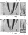
- FIGS. 3 ( a ) and 3 ( b ) respectively illustrate power density distribution in the xz-plane and the schematic distribution of the multiple NJ generated by a first exemplary structure of FIG. 1 ;
- FIGS. 4 ( a ) and 4 ( b ) respectively illustrate power density distribution in the xz-plane and the schematic distribution of the multiple NJ generated by a second exemplary structure of FIG. 1 ;
- FIG. 5 presents the power density distribution along X-coordinate for different values of refractive index n 3 for an exemplary structure of FIG. 1 ;
- FIG. 6 provides a cross-section view of a double-material structure with nonvertical edges
- FIG. 7 illustrates the power density distribution along x-axis for an exemplary system of FIG. 6 ;
- FIG. 8 ( a ) and ( b ) present different cross section of grating lines or unit cells according to one embodiment of the disclosure
- FIG. 9 ( a ) and ( b ) present different possible geometries of diffraction gratings according to one embodiment of the disclosure.
- the general principle of the present disclosure relies on the design of a diffraction grating containing structures or unit cells, which combines different dielectric materials to control the position of a focused nanojet beam, and change the direction of the NJ beam orientation.
- it is possible to achieve maximum efficiency in the desired diffraction order by changing the materials and dimensions of the constitutive parts of such a device.
- such a general principle consists in designing a NJ beam forming element (also called hereafter a microlens), to be considered as the elements of the diffraction grating unit cell as a combination of at least two dielectric materials with different refractive indexes having a nonsymmetrical system in a vertical cross-section.
- a microlens also called hereafter a microlens
- microlenses having such a topology are referred to as microlenses based on a combination of different materials, or also double-material microlenses, in contrast to single-material NJ microlenses presented in patent document EP 3 223 063. This transformation results in a deviation of a focused NJ beam.
- Such a component enabling control over the NJ beam direction, may be of interest for a number of applications requiring precise near-field patterning and/or deviation of an incident electromagnetic wave (e.g. visible light) propagation direction.
- An incident electromagnetic wave e.g. visible light
- a potential additional advantage of the proposed combined microlens is the possibility to change the position of the NJ hot spot.
- the diffraction grating containing such type of elements may find applications in glasses or solar panels for example.
- FIG. 1 illustrates the cross-section view, in a XZ plane of a double-material microlens or unit cell 10 which represents the constitutive part of the diffraction grating according to an embodiment of the present disclosure.
- Such a double-material microlens or unit cell 10 in cross-section view, corresponds to a combination of two different blocks of materials, referenced 12 and 13 .
- Their cross-section is rectangular (as illustrated in FIG. 1 ), but could also be trapezoidal or cuboid-shaped.
- Blocks referenced 12 and 13 respectively have refractive indexes n 2 and n 3 (n 2 >n 3 ) embedded in a homogeneous dielectric host medium 11 with a refractive index n 1 ⁇ n 3 .
- n 2 and n 3 refractive indexes n 2 and n 3 (n 2 >n 3 ) embedded in a homogeneous dielectric host medium 11 with a refractive index n 1 ⁇ n 3 .
- Blocks 12 and 13 could also be placed on a dielectric substrate (not illustrated) acting as a support layer.
- Block 12 has a width W 1 and a height H, while block 13 has a width W 2 and the same height H.
- base angle ⁇ 90°.
- some prismatic structures can also be used. Variation of the base angle value provides additional degree of freedom in the control of the NJ beam radiation, as discussed hereafter in relation to FIGS. 16 to 21 .
- the double-material microlens 10 is illuminated from below by an incident electromagnetic wave 14 , with a free-space wavelength ⁇ , which is the operating wavelength of the optical device 10 .
- the electromagnetic wave is illustrated with a direction parallel to the z-axis.
- a monochromatic (single wavelength) wave may be considered as a superposition of two waves with different polarizations, i.e. both a TE and a TM polarizations.
- the wave 14 is defined according to its propagation direction and polarization.
- the materials and size of the constitutive parts 11 , 12 and 13 can be optimized in order to manage the position of a NJ hot spot, intensity, direction and angle of deviation of a NJ beam.
- the inventors of the present disclosure have found out that diffraction of a plane wave on a microlens 10 based on the combination of different dielectric materials, can result in the deviation of the NJ away from the normal direction.
- the position of focal spot, angle of deviation, intensity and shape of NJ beam can be controlled by the variation of the refractive indexes n 1 , n 2 , n 3 and sizes (W 1 , W 2 , H) of the constitutive parts/blocks 12 , 13 .
- the NJ beam can be shifted from the axis of symmetry of the system by tuning the parameters of the blocks 12 , 13 .
- the beam-forming phenomenon appears on an edge between two materials of different refractive indexes, and is associated solely with this edge.
- the ratio of refractive indexes between both materials contributes to controlling an elevation angle of the generated nanojet beam, which is an angular position of a projection of the NJ beam in the vertical xz plane.
- the NJ beam radiation angle is defined by the Snell's law and can be determined using the approximate formula:
- n 1 the refractive index of the host medium 11
- n 2 the refractive index of the microlens material.
- the point of intersection of two equal NJ beams radiated from the opposite sides of the element determines the focal length of the NJ microlens.
- the focal length of the NJ lens can be characterized as the function of the size (width) and index ratio of the media inside and outside the lens. The total radiated NJ beam will be directed along the symmetry axis of the system.
- the focal length of such a microlens can be estimated as:
- W 1 is the width of a single element.
- TIR ⁇ ⁇ 2 sin - 1 ⁇ ( n 3 n 2 ) .
- the NJ beam radiation angle at the third edge, between block 13 and host medium 11 corresponds to:
- TIR ⁇ ⁇ 3 sin - 1 ⁇ ( n 1 n 3 ) .
- the three nanojet beams generated at the boundaries between the materials of different refractive indexes of optical device 10 may partially or totally combine, to produce a total focused beam, which corresponds to the interference pattern caused by the three primary nanojet beams associated with the three edges of device 10 .
- the point A of first (NJ 1 ) and second (NJ 2 ) NJs' intersection has the coordinates (W A ,H A ), where:
- Angle ⁇ B4 indicates the angle of deviation of the focal point A from the axis of symmetry parallel to the z-axis for the first block 12 with width W 1 :
- Angle ⁇ B5 shows the angle of deviation of the focal point B from the axis of symmetry parallel to the z-axis for the whole microlens 10 with total width W 1 +W 2 :
- FIG. 3 ( a ) several nanojet beams or hot spots may be observed. Actually, the interaction of the three primary nanojets NJ 1 , NJ 2 and NJ 3 creates three beams 30 , 31 , 32 in the example of FIG.
- Beams 31 and 32 are secondary beams, which are observe outside the blocks 12 , 13 .
- Beam 30 is the result of interference of the three primary nanojet beams NJ 1 , NJ 2 and NJ 3 and is thus considered as the main generated focused beam, which takes birth inside the microlens 10 but is also observed outside the blocks 12 , 13 .
- shift of the position of the total generated focused beam it is meant here, and throughout this document, a shift along x-axis.
- FIG. 3 ( b ) presents the schematic distribution of the multiple NJ generated by microlens 10 .
- n 3 ⁇ square root over (n 1 n 2 ) ⁇ the position of the hot spot (corresponding to the peak of field intensity within the nanojet beam) of the total generated NJ beam 30 will be close to the point A (point of first and second NJs' intersection NJ 1 and NJ 2 ).
- Varying the refractive index n 3 of the second block 13 of the system 10 we can tune the position of the hot spot of the total generated beam 30 .
- n 3 When increasing refractive index n 3 , we increase the shift of generated NJ 30 (decrease W A ) and H A .
- the resulting beam 30 will almost not be sensitive to the influence of NJ 3 . This fact can be explained by the relatively small intensity of NJ 3 .
- the sizes of constitutive elements 12 , 13 have strong impact on the behavior of the total generated NJ beam 30 .
- FIG. 6 This cross-section view may correspond to the double-material prismatic system embedded in a homogeneous dielectric host media with a refractive index n 1 ⁇ n 2 ⁇ n 3 .
- the NJ beam radiation angle can be determined using the approximate formula (12):
- the optical device 10 which is based on a non-symmetrical structure relying on a combination of different dielectric materials, provides a unique set of optical functions, including focusing and shifting. Moreover, it shows a simple topology, compatible with established planar micro/nano fabrication methods, e.g. nanoimprinting and photolithography.
- Such an optical device 10 relies on the fact that three NJ beams, originating from different edges (associated with different blocks/layers) of the microstructure, recombine and contribute to the formation of a total NJ beam deflected from the normal direction.
- Such an microlens allows generating a NJ beam shift, with respect to the central vertical axis of symmetry of the cross-section of device 10 in the xz-plane.
- the NJ hot spot position is not sensitive to the height H of the system for all values of refractive indexes of dielectric materials.
- the total response of the system is almost independent on the wavelength ⁇ of incident electromagnetic wave 14 .
- FIG. 8 ( a ) shows the diffraction grating with double-material elements embedded into a dielectric material with refractive index n 1 .
- the grating constant or the period of the grating is d.
- a linearly-polarized plane wave is normally incident on the grating from the top in a plane perpendicular to the grating.
- Angles of the diffracted beams are not influenced by the structure of the double-material elements. They are determined by the period of the grating, wavelength of the incident plane wave and angle of wave incidence. Hence, they can be calculated according to the grating equation.
- the performance of the grating depends on the polarization of the incident wave and parameters (dimensions, form and material) of the elements. Unlike the diffraction grating containing symmetrical single-material elements (regular structure of the same spacing), the proposed diffraction grating based on the double-material elements achieves nonsymmetrical distribution of an intensity (Tj ⁇ T-j, Rj ⁇ R-j, . . . , where j is the number of diffraction order) leading to the maximal grating efficiency for the desired diffraction order. In the case of elements with W ⁇ the maximal input corresponds to the orders ⁇ 1.
- the diffraction grating comprises the layer forming a substrate for the double-material elements.
- the refractive index of the substrate is n 4 .
- FIGS. 9 ( a ) and 9 ( b ) The possible realization of the gratings in 3D space is presented in FIGS. 9 ( a ) and 9 ( b ) .
- the full-wave electromagnetic analysis was done for the 2D array of double-material elements ( FIG. 9 ( a ) ). We assumed that the system is infinite in X-direction.
- Such a diffraction grating consists in flat shallow structures.
- the advantage is ease of fabrication and robustness of the structure.
- the system could be used in all optical systems that would need to deviate an image or some light with a micro-structure, the advantage being simplicity of fabrication and robustness.
- Typical application domains are head-up displays, solar cell panels for maximizing light collection, OLED display light extraction, among many others.
Landscapes
- Physics & Mathematics (AREA)
- General Physics & Mathematics (AREA)
- Optics & Photonics (AREA)
- Spectroscopy & Molecular Physics (AREA)
- Diffracting Gratings Or Hologram Optical Elements (AREA)
Abstract
Description
-
- a first edge between said host medium and said first block along said z-axis that is targeted to form a first beam in a near field zone, being a first nanojet;
- a second edge between said first block and said second block along said z-axis that is targeted to form a second beam in said near field zone, being a second nanojet;
- a third edge between said second block and said host medium along said z-axis that is targeted to form a third beam in said near field zone, being a third nanojet,
and wherein a shift of position along said x-axis and/or an angle of deviation from said z-axis in said vertical xz plane of a beam resulting from an at least partial combination of said first, second and third beams depend on said first, second and third refractive indexes n1, n2 n3, said widths and heights of said first and second blocks in said cross-section and said base angles.
-
- glass;
- plastic;
- a polymer material;
- oxide;
- nitride.
where
is the critical angle of refraction, n1 is the refractive index of the
where
W1 is the width of a single element.
where
Here
Angle ΘB4 indicates the angle of deviation of the focal point A from the axis of symmetry parallel to the z-axis for the
Angle ΘB5 shows the angle of deviation of the focal point B from the axis of symmetry parallel to the z-axis for the
and the angle ΘB6 of a focal point deviation for the
In this case, all three beams NJ1, NJ2 and NJ3 make an input into the total generated beam by
Here Θ′TIRj are the critical angles of refraction from the nonvertical edges. To get the approximate formula for Θ′TIRj we should just take into account the changing of the position of the edge. As the result, the NJ beam radiation angle can be estimated as:
Claims (17)
Applications Claiming Priority (4)
| Application Number | Priority Date | Filing Date | Title |
|---|---|---|---|
| EP18305263.8A EP3540479A1 (en) | 2018-03-13 | 2018-03-13 | Diffraction grating comprising double-materials structures |
| EP18305263 | 2018-03-13 | ||
| EP18305263.8 | 2018-03-13 | ||
| PCT/EP2019/055679 WO2019175010A1 (en) | 2018-03-13 | 2019-03-07 | Diffraction grating comprising double-materials structures |
Publications (2)
| Publication Number | Publication Date |
|---|---|
| US20210041609A1 US20210041609A1 (en) | 2021-02-11 |
| US11573356B2 true US11573356B2 (en) | 2023-02-07 |
Family
ID=62636126
Family Applications (1)
| Application Number | Title | Priority Date | Filing Date |
|---|---|---|---|
| US16/980,307 Active US11573356B2 (en) | 2018-03-13 | 2019-03-07 | Diffraction grating comprising double-materials structures |
Country Status (5)
| Country | Link |
|---|---|
| US (1) | US11573356B2 (en) |
| EP (2) | EP3540479A1 (en) |
| KR (1) | KR102579589B1 (en) |
| CN (1) | CN112601990B (en) |
| WO (1) | WO2019175010A1 (en) |
Cited By (5)
| Publication number | Priority date | Publication date | Assignee | Title |
|---|---|---|---|---|
| US20210233291A1 (en) * | 2018-07-02 | 2021-07-29 | Interdigital Ce Patent Holdings | Image sensor comprising a color splitter with two different refractive indexes, and different height |
| US20220059250A1 (en) * | 2018-12-18 | 2022-02-24 | Interdigital Ce Patent Holdings, Sas | Optical manipulation apparatus |
| US12174512B2 (en) | 2018-12-18 | 2024-12-24 | Interdigital Ce Patent Holdings | Device for forming an outgoing electromagnetic wave from an incident electromagnetic wave |
| US12210155B2 (en) | 2018-06-29 | 2025-01-28 | Interdigital Ce Patent Holdings | Optical device comprising a multi-layers waveguides |
| US12228756B2 (en) | 2018-12-21 | 2025-02-18 | Interdigital Ce Patent Holdings, Sas | Optical device |
Families Citing this family (15)
| Publication number | Priority date | Publication date | Assignee | Title |
|---|---|---|---|---|
| EP3540499A1 (en) | 2018-03-13 | 2019-09-18 | Thomson Licensing | Image sensor comprising a color splitter with two different refractive indexes |
| EP3540479A1 (en) | 2018-03-13 | 2019-09-18 | Thomson Licensing | Diffraction grating comprising double-materials structures |
| EP3633438A1 (en) | 2018-10-01 | 2020-04-08 | InterDigital CE Patent Holdings | Inhomogeneous microlens device for near-field focusing, beam forming, and high-efficiency far-field device implementation |
| EP3633437A1 (en) | 2018-10-01 | 2020-04-08 | InterDigital CE Patent Holdings | Device for near-field focusing and beam forming |
| EP4127820A1 (en) | 2020-03-23 | 2023-02-08 | InterDigital CE Patent Holdings, SAS | Waveguide display system with wide field of view |
| EP4127789B1 (en) * | 2020-03-23 | 2025-04-30 | InterDigital CE Patent Holdings, SAS | Unpolarized light grating in-coupler |
| DE102020110173B4 (en) | 2020-04-14 | 2021-11-25 | Helmholtz-Zentrum Berlin für Materialien und Energie Gesellschaft mit beschränkter Haftung | Diffraction grating and method of using the diffraction grating |
| EP4154043B1 (en) | 2020-05-22 | 2025-05-14 | InterDigital CE Patent Holdings, SAS | High color uniformity double material diffraction grating comprising step-like cavities |
| CN116075938A (en) | 2020-07-30 | 2023-05-05 | 交互数字Ce专利控股有限公司 | Optical component and image sensor including optical component |
| CN113054044B (en) * | 2021-03-08 | 2022-08-05 | 合肥工业大学 | Monocrystalline silicon thin-film solar cell with double-layer period unmatched rotating rectangular grating structure |
| CN114114481B (en) * | 2021-12-15 | 2023-05-26 | 中国科学院光电技术研究所 | Preparation method and application of super-resolution lens based on metal-medium strip array |
| CN114721071B (en) * | 2022-03-15 | 2025-04-29 | 苏州山河光电科技有限公司 | A super surface optical device and its manufacturing process |
| KR20240039963A (en) * | 2022-09-20 | 2024-03-27 | 주식회사 엘지유플러스 | Optical Device and Virtual Image Display Method Using the Same |
| CN115857078B (en) * | 2022-11-15 | 2025-04-01 | 中山大学 | A nano-supergrating and optical quantum computing device |
| CN116429730B (en) * | 2023-04-21 | 2025-09-19 | 聊城大学 | Pea-type super-surface-based optical refractive index sensor and manufacturing method thereof |
Citations (73)
| Publication number | Priority date | Publication date | Assignee | Title |
|---|---|---|---|---|
| US3718383A (en) | 1971-04-19 | 1973-02-27 | Eastman Kodak Co | Plastic optical element having refractive index gradient |
| US6099146A (en) | 1997-02-04 | 2000-08-08 | Olympus Optical Company, Ltd. | Illuminating optical system for cutting infrared light by relief type optical element |
| WO2003007032A1 (en) | 2001-07-10 | 2003-01-23 | Sumitomo Electric Industries, Ltd. | Optical waveguide diffraction grating device and its fabrication method |
| US20050002611A1 (en) | 2003-05-13 | 2005-01-06 | Nokia Corporation | Method and optical system for coupling light into a waveguide |
| CN1606704A (en) | 2002-09-19 | 2005-04-13 | 住友电气工业株式会社 | Diffractive optical device and method for manufacturing said optical device |
| CN1661478A (en) | 2004-02-26 | 2005-08-31 | Asml荷兰有限公司 | Stationary and dynamic radial transverse electric polarizer for high numerical aperture systems |
| US20060124833A1 (en) | 2004-12-10 | 2006-06-15 | Atsushi Toda | Method and apparatus for acquiring physical information, method for manufacturing semiconductor device including array of plurality of unit components for detecting physical quantity distribution, light-receiving device and manufacturing method therefor, and solid-state imaging device and manufacturing method therefor |
| WO2007031991A2 (en) | 2005-09-14 | 2007-03-22 | Mirage Innovations Ltd. | Diffractive optical device and system |
| US7394535B1 (en) | 2007-03-20 | 2008-07-01 | Tokyo Electron Limited | Optical metrology using a photonic nanojet |
| WO2009083977A2 (en) | 2008-01-02 | 2009-07-09 | Mirage Innovations Ltd. | Optical device for relaying polychromatic light |
| US20090190094A1 (en) | 2006-09-28 | 2009-07-30 | Brother Kogyo Kabushiki Kaisha | Optical system for light flux transfer, and retinal scanning display using such an optical system |
| EP2196729A1 (en) | 2008-12-12 | 2010-06-16 | BAE Systems PLC | Improvements in or relating to waveguides |
| US20110235166A1 (en) | 2008-10-17 | 2011-09-29 | The Arizona Board of Regents on Behalf of the Univerity of Arizona | Apparatus and Method of Generating Nearly Non-Diffracting Beams from Multimode Optical Fibers |
| US20130099343A1 (en) | 2010-07-02 | 2013-04-25 | Panasonic Corporation | Solid-state imaging device |
| US20130250421A1 (en) | 2012-03-26 | 2013-09-26 | Asahi Glass Company, Limited | Transmission diffraction element |
| US20130322810A1 (en) | 2012-06-04 | 2013-12-05 | Steven John Robbins | Multiple waveguide imaging structure |
| WO2014036537A1 (en) | 2012-08-31 | 2014-03-06 | Nguyen Ian A | Polarization system for wavelength pass-through in a near-to-eye display |
| WO2014044912A1 (en) | 2012-09-20 | 2014-03-27 | Teknologian Tutkimuskeskus Vtt | Optical device with diffractive grating |
| US20150063753A1 (en) | 2013-09-05 | 2015-03-05 | Southern Methodist University | Enhanced coupling strength gratings |
| US9099370B2 (en) | 2012-09-03 | 2015-08-04 | Panasonic Intellectual Property Management Co., Ltd. | Solid-state imaging element and imaging device |
| US9140602B2 (en) | 2012-08-11 | 2015-09-22 | The Board Of Trustees Of The Leland Stanford Junior University | Nanophotonic light-field sensor |
| US20150286060A1 (en) | 2014-04-07 | 2015-10-08 | Samsung Electronics Co., Ltd. | Color separation device and image sensor including the color separation device |
| US20150323800A1 (en) | 2014-05-09 | 2015-11-12 | Samsung Electronics Co., Ltd. | Color separation devices and image sensors including the same |
| EP2955753A2 (en) | 2014-06-13 | 2015-12-16 | Samsung Electronics Co., Ltd | Stacked type image sensor including color separation element and image pickup apparatus including the stacked type image sensor |
| US20150362641A1 (en) * | 2014-06-13 | 2015-12-17 | The Regents Of The University Of California | High Index Contrast Grating Structure for Light Manipulation and Related Method |
| GB2529003A (en) | 2014-08-03 | 2016-02-10 | Wave Optics Ltd | Optical device |
| US20160054172A1 (en) | 2014-08-22 | 2016-02-25 | Samsung Electronics Co., Ltd. | Image sensor for producing vivid colors and method of manufacturing the same |
| US20160064172A1 (en) | 2014-09-02 | 2016-03-03 | Delta Systems, Inc. | Plunger switch assembly and method of operation |
| US20160070062A1 (en) | 2013-04-22 | 2016-03-10 | Cornell University | Athermal optical devices based on composite structures |
| US9383582B2 (en) | 2006-10-13 | 2016-07-05 | Apple Inc. | Peripheral treatment for head-mounted displays |
| US20160231568A1 (en) | 2015-02-09 | 2016-08-11 | Microsoft Technology Licensing, Llc | Waveguide |
| US9419036B2 (en) | 2012-10-18 | 2016-08-16 | Panasonic Intellectual Property Management Co., Ltd. | Solid-state imaging device |
| US20170006278A1 (en) | 2015-06-30 | 2017-01-05 | Thomson Licensing | Plenoptic foveated camera |
| US20170012078A1 (en) | 2015-07-08 | 2017-01-12 | Samsung Electronics Co., Ltd. | Method of manufacturing image sensor including nanostructure color filter |
| US9564469B2 (en) | 2014-08-21 | 2017-02-07 | Samsung Electronics Co., Ltd. | Image sensor comprising a color separation device separating incident light into plural of colors for having improved light utilization efficiency and method of manufacturing the same |
| US20170090206A1 (en) | 2015-09-30 | 2017-03-30 | Samsung Electronics Co., Ltd. | Color splitter structure, method of manufacturing the same, image sensor including color splitter structure, and optical apparatus including image sensor |
| US20170092668A1 (en) | 2015-09-24 | 2017-03-30 | Samsung Electronics Co., Ltd. | Optical apparatus including optical functional layer having high refractive index and method of manufacturing the optical apparatus |
| US20170092676A1 (en) | 2015-09-25 | 2017-03-30 | Samsung Electronics Co., Ltd. | Image sensor including color separation element and image pickup apparatus including the image sensor |
| US20170097510A1 (en) | 2015-10-06 | 2017-04-06 | Samsung Electronics Co., Ltd. | Image sensor and method of manufacturing the same |
| US20170098672A1 (en) | 2015-10-06 | 2017-04-06 | Samsung Electronics Co., Ltd. | Image sensor including color separation element |
| CN106772734A (en) | 2017-01-03 | 2017-05-31 | 中国科学院上海光学精密机械研究所 | The asymmetric pattern reflection type optical grid of broadband high-diffraction efficiency |
| US20170179178A1 (en) | 2015-12-22 | 2017-06-22 | Samsung Electronics Co., Ltd. | Color separation element array, image sensor including the same, and electronic device |
| WO2017116637A1 (en) | 2015-12-29 | 2017-07-06 | Microsoft Technology Licensing, Llc | Augmented reality display system with variable focus |
| US20170212348A1 (en) | 2016-01-27 | 2017-07-27 | Yijing Fu | Mixed environment display device and waveguide cross-coupling suppressors |
| US9766467B2 (en) | 2014-10-20 | 2017-09-19 | Samsung Electronics Co., Ltd. | Color splitter, method of manufacturing the same, and image sensor including the same |
| EP3223063A1 (en) | 2016-03-24 | 2017-09-27 | Thomson Licensing | Device for forming a field intensity pattern in the near zone, from incident electromagnetic waves |
| EP3223062A1 (en) * | 2016-03-24 | 2017-09-27 | Thomson Licensing | Device for forming at least one focused beam in the near zone, from incident electromagnetic waves |
| WO2017180403A1 (en) | 2016-04-13 | 2017-10-19 | Microsoft Technology Licensing, Llc | Waveguides with extended field of view |
| US20170307886A1 (en) | 2016-04-25 | 2017-10-26 | Petri Antero Stenberg | Refractive coating for diffractive optical elements |
| EP3240046A1 (en) | 2016-04-29 | 2017-11-01 | BASF Coatings GmbH | Solar light collector |
| US20170315346A1 (en) | 2016-04-29 | 2017-11-02 | Jani Kari Tapio Tervo | Robust Architecture for Large Field of View Components |
| US9891436B2 (en) | 2016-02-11 | 2018-02-13 | Microsoft Technology Licensing, Llc | Waveguide-based displays with anti-reflective and highly-reflective coating |
| EP3312660A1 (en) | 2016-10-21 | 2018-04-25 | Thomson Licensing | Device for forming at least one tilted focused beam in the near zone, from incident electromagnetic waves |
| EP3312646A1 (en) | 2016-10-21 | 2018-04-25 | Thomson Licensing | Device and method for shielding at least one sub-wavelength-scale object from an incident electromagnetic wave |
| EP3312674A1 (en) | 2016-10-21 | 2018-04-25 | Thomson Licensing | A photolithography device for generating pattern on a photoresist substrate |
| US20180113313A1 (en) | 2016-10-26 | 2018-04-26 | Magic Leap, Inc. | Outcoupling grating for augmented reality system |
| WO2018102582A1 (en) | 2016-12-01 | 2018-06-07 | Magic Leap, Inc. | Projector with scanning array light engine |
| WO2018102834A2 (en) | 2016-12-02 | 2018-06-07 | Digilens, Inc. | Waveguide device with uniform output illumination |
| EP3339938A1 (en) | 2015-08-20 | 2018-06-27 | Hoya Lens Thailand Ltd. | Optical device |
| US20180231771A1 (en) | 2017-02-15 | 2018-08-16 | Magic Leap, Inc. | Projector architecture incorporating artifact mitigation |
| EP3385219A1 (en) | 2017-04-07 | 2018-10-10 | Thomson Licensing | Method for manufacturing a device for forming at least one focused beam in a near zone |
| US20190121239A1 (en) | 2017-10-20 | 2019-04-25 | Magic Leap, Inc. | Configuring optical layers in imprint lithography processes |
| EP3499278A1 (en) | 2017-12-13 | 2019-06-19 | Thomson Licensing | A diffraction grating structure comprising several grating lines |
| EP3540499A1 (en) | 2018-03-13 | 2019-09-18 | Thomson Licensing | Image sensor comprising a color splitter with two different refractive indexes |
| EP3540479A1 (en) | 2018-03-13 | 2019-09-18 | Thomson Licensing | Diffraction grating comprising double-materials structures |
| EP3588150A1 (en) | 2018-06-29 | 2020-01-01 | Thomson Licensing | An optical device comprising multi-layer waveguides |
| EP3591700A1 (en) | 2018-07-02 | 2020-01-08 | Thomson Licensing | Image sensor comprising a color splitter with two different refractive indexes, and different height |
| US10534115B1 (en) | 2017-09-22 | 2020-01-14 | Facebook Technologies, Llc | Gray-tone electron-beam lithography |
| EP3671293A1 (en) | 2018-12-21 | 2020-06-24 | Thomson Licensing | An optical device comprising at least one diffraction grating having a grating pitch above the wavelength |
| EP3671322A1 (en) | 2018-12-18 | 2020-06-24 | Thomson Licensing | Device for forming an outgoing electromagnetic wave from an incident electromagnetic wave |
| US10866360B2 (en) * | 2015-08-19 | 2020-12-15 | President And Fellows Of Harvard College | Broadband multifunctional efficient meta-gratings based on dielectric waveguide phase shifters |
| WO2021053182A1 (en) | 2019-09-19 | 2021-03-25 | Interdigital Ce Patent Holdings | Optical device for coupling a high field of view of incident light |
| US11204452B2 (en) * | 2016-10-05 | 2021-12-21 | Agency For Science, Technology And Research | Diffractive optical element and method of forming thereof |
Family Cites Families (2)
| Publication number | Priority date | Publication date | Assignee | Title |
|---|---|---|---|---|
| FR2998979B1 (en) * | 2012-11-30 | 2017-09-08 | Office National Detudes Et De Rech Aerospatiales Onera | DEVICE FOR CONTROLLING THE PHASE OF AN OPTICAL WAVEFRONT |
| JP2014134564A (en) | 2013-01-08 | 2014-07-24 | Canon Inc | Absorption type wire grid polarization element and optical instrument |
-
2018
- 2018-03-13 EP EP18305263.8A patent/EP3540479A1/en not_active Withdrawn
-
2019
- 2019-03-07 CN CN201980031384.4A patent/CN112601990B/en active Active
- 2019-03-07 KR KR1020207027368A patent/KR102579589B1/en active Active
- 2019-03-07 WO PCT/EP2019/055679 patent/WO2019175010A1/en not_active Ceased
- 2019-03-07 US US16/980,307 patent/US11573356B2/en active Active
- 2019-03-07 EP EP19708329.8A patent/EP3765873B1/en active Active
Patent Citations (84)
| Publication number | Priority date | Publication date | Assignee | Title |
|---|---|---|---|---|
| US3718383A (en) | 1971-04-19 | 1973-02-27 | Eastman Kodak Co | Plastic optical element having refractive index gradient |
| US6099146A (en) | 1997-02-04 | 2000-08-08 | Olympus Optical Company, Ltd. | Illuminating optical system for cutting infrared light by relief type optical element |
| WO2003007032A1 (en) | 2001-07-10 | 2003-01-23 | Sumitomo Electric Industries, Ltd. | Optical waveguide diffraction grating device and its fabrication method |
| EP1406098A1 (en) | 2001-07-10 | 2004-04-07 | Sumitomo Electric Industries, Ltd. | Optical waveguide diffraction grating device and its fabrication method |
| CN1606704A (en) | 2002-09-19 | 2005-04-13 | 住友电气工业株式会社 | Diffractive optical device and method for manufacturing said optical device |
| EP1542043A1 (en) | 2002-09-19 | 2005-06-15 | Sumitomo Electric Industries, Ltd. | Diffractive optical device and method for producing same |
| US20050002611A1 (en) | 2003-05-13 | 2005-01-06 | Nokia Corporation | Method and optical system for coupling light into a waveguide |
| CN1661478A (en) | 2004-02-26 | 2005-08-31 | Asml荷兰有限公司 | Stationary and dynamic radial transverse electric polarizer for high numerical aperture systems |
| US20060124833A1 (en) | 2004-12-10 | 2006-06-15 | Atsushi Toda | Method and apparatus for acquiring physical information, method for manufacturing semiconductor device including array of plurality of unit components for detecting physical quantity distribution, light-receiving device and manufacturing method therefor, and solid-state imaging device and manufacturing method therefor |
| WO2007031991A2 (en) | 2005-09-14 | 2007-03-22 | Mirage Innovations Ltd. | Diffractive optical device and system |
| US20090190094A1 (en) | 2006-09-28 | 2009-07-30 | Brother Kogyo Kabushiki Kaisha | Optical system for light flux transfer, and retinal scanning display using such an optical system |
| US9383582B2 (en) | 2006-10-13 | 2016-07-05 | Apple Inc. | Peripheral treatment for head-mounted displays |
| US7394535B1 (en) | 2007-03-20 | 2008-07-01 | Tokyo Electron Limited | Optical metrology using a photonic nanojet |
| WO2009083977A2 (en) | 2008-01-02 | 2009-07-09 | Mirage Innovations Ltd. | Optical device for relaying polychromatic light |
| US20110235166A1 (en) | 2008-10-17 | 2011-09-29 | The Arizona Board of Regents on Behalf of the Univerity of Arizona | Apparatus and Method of Generating Nearly Non-Diffracting Beams from Multimode Optical Fibers |
| EP2196729A1 (en) | 2008-12-12 | 2010-06-16 | BAE Systems PLC | Improvements in or relating to waveguides |
| US20130099343A1 (en) | 2010-07-02 | 2013-04-25 | Panasonic Corporation | Solid-state imaging device |
| US20130250421A1 (en) | 2012-03-26 | 2013-09-26 | Asahi Glass Company, Limited | Transmission diffraction element |
| US20130322810A1 (en) | 2012-06-04 | 2013-12-05 | Steven John Robbins | Multiple waveguide imaging structure |
| US9140602B2 (en) | 2012-08-11 | 2015-09-22 | The Board Of Trustees Of The Leland Stanford Junior University | Nanophotonic light-field sensor |
| WO2014036537A1 (en) | 2012-08-31 | 2014-03-06 | Nguyen Ian A | Polarization system for wavelength pass-through in a near-to-eye display |
| US8885997B2 (en) | 2012-08-31 | 2014-11-11 | Microsoft Corporation | NED polarization system for wavelength pass-through |
| US9099370B2 (en) | 2012-09-03 | 2015-08-04 | Panasonic Intellectual Property Management Co., Ltd. | Solid-state imaging element and imaging device |
| WO2014044912A1 (en) | 2012-09-20 | 2014-03-27 | Teknologian Tutkimuskeskus Vtt | Optical device with diffractive grating |
| US9419036B2 (en) | 2012-10-18 | 2016-08-16 | Panasonic Intellectual Property Management Co., Ltd. | Solid-state imaging device |
| US20160070062A1 (en) | 2013-04-22 | 2016-03-10 | Cornell University | Athermal optical devices based on composite structures |
| US20150063753A1 (en) | 2013-09-05 | 2015-03-05 | Southern Methodist University | Enhanced coupling strength gratings |
| US20150286060A1 (en) | 2014-04-07 | 2015-10-08 | Samsung Electronics Co., Ltd. | Color separation device and image sensor including the color separation device |
| US20150323800A1 (en) | 2014-05-09 | 2015-11-12 | Samsung Electronics Co., Ltd. | Color separation devices and image sensors including the same |
| EP2955753A2 (en) | 2014-06-13 | 2015-12-16 | Samsung Electronics Co., Ltd | Stacked type image sensor including color separation element and image pickup apparatus including the stacked type image sensor |
| US20150362641A1 (en) * | 2014-06-13 | 2015-12-17 | The Regents Of The University Of California | High Index Contrast Grating Structure for Light Manipulation and Related Method |
| GB2529003A (en) | 2014-08-03 | 2016-02-10 | Wave Optics Ltd | Optical device |
| US9564469B2 (en) | 2014-08-21 | 2017-02-07 | Samsung Electronics Co., Ltd. | Image sensor comprising a color separation device separating incident light into plural of colors for having improved light utilization efficiency and method of manufacturing the same |
| US20160054172A1 (en) | 2014-08-22 | 2016-02-25 | Samsung Electronics Co., Ltd. | Image sensor for producing vivid colors and method of manufacturing the same |
| US20160064172A1 (en) | 2014-09-02 | 2016-03-03 | Delta Systems, Inc. | Plunger switch assembly and method of operation |
| US9766467B2 (en) | 2014-10-20 | 2017-09-19 | Samsung Electronics Co., Ltd. | Color splitter, method of manufacturing the same, and image sensor including the same |
| US20160231568A1 (en) | 2015-02-09 | 2016-08-11 | Microsoft Technology Licensing, Llc | Waveguide |
| US20170006278A1 (en) | 2015-06-30 | 2017-01-05 | Thomson Licensing | Plenoptic foveated camera |
| CN106331445A (en) | 2015-06-30 | 2017-01-11 | 汤姆逊许可公司 | plenoptic concave camera |
| US20170012078A1 (en) | 2015-07-08 | 2017-01-12 | Samsung Electronics Co., Ltd. | Method of manufacturing image sensor including nanostructure color filter |
| US10866360B2 (en) * | 2015-08-19 | 2020-12-15 | President And Fellows Of Harvard College | Broadband multifunctional efficient meta-gratings based on dielectric waveguide phase shifters |
| EP3339938A1 (en) | 2015-08-20 | 2018-06-27 | Hoya Lens Thailand Ltd. | Optical device |
| US20170092668A1 (en) | 2015-09-24 | 2017-03-30 | Samsung Electronics Co., Ltd. | Optical apparatus including optical functional layer having high refractive index and method of manufacturing the optical apparatus |
| US20170092676A1 (en) | 2015-09-25 | 2017-03-30 | Samsung Electronics Co., Ltd. | Image sensor including color separation element and image pickup apparatus including the image sensor |
| US20170090206A1 (en) | 2015-09-30 | 2017-03-30 | Samsung Electronics Co., Ltd. | Color splitter structure, method of manufacturing the same, image sensor including color splitter structure, and optical apparatus including image sensor |
| US20170097510A1 (en) | 2015-10-06 | 2017-04-06 | Samsung Electronics Co., Ltd. | Image sensor and method of manufacturing the same |
| US20170098672A1 (en) | 2015-10-06 | 2017-04-06 | Samsung Electronics Co., Ltd. | Image sensor including color separation element |
| CN106932845A (en) | 2015-12-22 | 2017-07-07 | 三星电子株式会社 | Color resolution element array, imageing sensor and electronic installation |
| US20170179178A1 (en) | 2015-12-22 | 2017-06-22 | Samsung Electronics Co., Ltd. | Color separation element array, image sensor including the same, and electronic device |
| WO2017116637A1 (en) | 2015-12-29 | 2017-07-06 | Microsoft Technology Licensing, Llc | Augmented reality display system with variable focus |
| US20170212348A1 (en) | 2016-01-27 | 2017-07-27 | Yijing Fu | Mixed environment display device and waveguide cross-coupling suppressors |
| WO2017131983A1 (en) | 2016-01-27 | 2017-08-03 | Microsoft Technology Licensing, Llc | Mixed environment display device and waveguide cross-coupling suppressors |
| US9891436B2 (en) | 2016-02-11 | 2018-02-13 | Microsoft Technology Licensing, Llc | Waveguide-based displays with anti-reflective and highly-reflective coating |
| EP3223062A1 (en) * | 2016-03-24 | 2017-09-27 | Thomson Licensing | Device for forming at least one focused beam in the near zone, from incident electromagnetic waves |
| WO2017162880A1 (en) | 2016-03-24 | 2017-09-28 | Thomson Licensing | Device for forming a field intensity pattern in the near zone, from incident electromagnetic waves |
| US20190101700A1 (en) | 2016-03-24 | 2019-04-04 | Thomson Licensing | Device for forming at least one focused beam in the near zone, from incident electromagnetic waves |
| WO2017162882A1 (en) | 2016-03-24 | 2017-09-28 | Thomson Licensing | Device for forming a field intensity pattern in the near zone, from incident electromagnetic waves |
| EP3223063A1 (en) | 2016-03-24 | 2017-09-27 | Thomson Licensing | Device for forming a field intensity pattern in the near zone, from incident electromagnetic waves |
| WO2017180403A1 (en) | 2016-04-13 | 2017-10-19 | Microsoft Technology Licensing, Llc | Waveguides with extended field of view |
| US20170307886A1 (en) | 2016-04-25 | 2017-10-26 | Petri Antero Stenberg | Refractive coating for diffractive optical elements |
| CN109073885A (en) | 2016-04-25 | 2018-12-21 | 微软技术许可有限责任公司 | Refractive Coatings for Diffractive Optical Elements |
| US20170315346A1 (en) | 2016-04-29 | 2017-11-02 | Jani Kari Tapio Tervo | Robust Architecture for Large Field of View Components |
| EP3240046A1 (en) | 2016-04-29 | 2017-11-01 | BASF Coatings GmbH | Solar light collector |
| US11204452B2 (en) * | 2016-10-05 | 2021-12-21 | Agency For Science, Technology And Research | Diffractive optical element and method of forming thereof |
| EP3312660A1 (en) | 2016-10-21 | 2018-04-25 | Thomson Licensing | Device for forming at least one tilted focused beam in the near zone, from incident electromagnetic waves |
| EP3312646A1 (en) | 2016-10-21 | 2018-04-25 | Thomson Licensing | Device and method for shielding at least one sub-wavelength-scale object from an incident electromagnetic wave |
| EP3312674A1 (en) | 2016-10-21 | 2018-04-25 | Thomson Licensing | A photolithography device for generating pattern on a photoresist substrate |
| US20180113313A1 (en) | 2016-10-26 | 2018-04-26 | Magic Leap, Inc. | Outcoupling grating for augmented reality system |
| WO2018102582A1 (en) | 2016-12-01 | 2018-06-07 | Magic Leap, Inc. | Projector with scanning array light engine |
| WO2018102834A2 (en) | 2016-12-02 | 2018-06-07 | Digilens, Inc. | Waveguide device with uniform output illumination |
| CN106772734A (en) | 2017-01-03 | 2017-05-31 | 中国科学院上海光学精密机械研究所 | The asymmetric pattern reflection type optical grid of broadband high-diffraction efficiency |
| US20180231771A1 (en) | 2017-02-15 | 2018-08-16 | Magic Leap, Inc. | Projector architecture incorporating artifact mitigation |
| EP3385219A1 (en) | 2017-04-07 | 2018-10-10 | Thomson Licensing | Method for manufacturing a device for forming at least one focused beam in a near zone |
| US10534115B1 (en) | 2017-09-22 | 2020-01-14 | Facebook Technologies, Llc | Gray-tone electron-beam lithography |
| US20190121239A1 (en) | 2017-10-20 | 2019-04-25 | Magic Leap, Inc. | Configuring optical layers in imprint lithography processes |
| EP3499278A1 (en) | 2017-12-13 | 2019-06-19 | Thomson Licensing | A diffraction grating structure comprising several grating lines |
| EP3540499A1 (en) | 2018-03-13 | 2019-09-18 | Thomson Licensing | Image sensor comprising a color splitter with two different refractive indexes |
| EP3540479A1 (en) | 2018-03-13 | 2019-09-18 | Thomson Licensing | Diffraction grating comprising double-materials structures |
| US20210041709A1 (en) | 2018-03-13 | 2021-02-11 | Interdigital Ce Patent Holdings | Image sensor comprising a color splitter with two different refractive indexes |
| EP3588150A1 (en) | 2018-06-29 | 2020-01-01 | Thomson Licensing | An optical device comprising multi-layer waveguides |
| EP3591700A1 (en) | 2018-07-02 | 2020-01-08 | Thomson Licensing | Image sensor comprising a color splitter with two different refractive indexes, and different height |
| EP3671322A1 (en) | 2018-12-18 | 2020-06-24 | Thomson Licensing | Device for forming an outgoing electromagnetic wave from an incident electromagnetic wave |
| EP3671293A1 (en) | 2018-12-21 | 2020-06-24 | Thomson Licensing | An optical device comprising at least one diffraction grating having a grating pitch above the wavelength |
| WO2021053182A1 (en) | 2019-09-19 | 2021-03-25 | Interdigital Ce Patent Holdings | Optical device for coupling a high field of view of incident light |
Non-Patent Citations (62)
| Title |
|---|
| Aieta, Francesco, et. al., "Multiwavelength Achromatic Metasurfaces By Dispersive Phase Compensation". Sciencexpress, 2015, (8 pages). |
| Ang, Angeleene S., et al., "‘Photonic Hook’ Based Optomechanical Nanoparticle Manipulator". Scientific Reports, vol. 8. No. 2029, Published online: Feb. 1, 2018, pp. 1-7. |
| Avayu, Ori, et al., "Composite Functional Metasurfaces For Multispectral Achromatic Optics". Nature Communications, 2017, pp. 1-7 (7 pages). |
| Boriskin, Artem, et. al., "Near Field Focusing By Edge Diffraction". Optics Letters, vol. 43, No. 16, Aug. 2018, pp. 4053-4056 (4 pages). |
| Chaumet, P. C., et. al., "Time-Averaged Total Force On A Dipolar Sphere In An Electromagnetic Field". Optics Letters, vol. 25, No. 15, (2000), pp. 1065-1067 (3 pages). |
| Chen, Q. et al., "Nanophotonic image sensors." Small 12, No. 36, 2016: 4922-4935 (14 pages). |
| Chen, Yiguo, et. al., "Engineering The Phase Front Of Light With Phase-Change Material Based Planar Lenses". Scientific Reports vol. 5, No. 1, Mar. 2, 2015, pp. 1-7. |
| Deng, Zi-Lan, et. al., "Wide-Angle And High-Efficiency Achromatic Metasurfaces For Visible Light". Optical Express, vol. 24, No. 20 pp. 23118-23128 (12 pages). |
| Devilez, Alexis, et. al., "Three-Dimensional Subwavelength Confinement Of Light With Dielectric Microspheres". Optics Express, vol. 17, No. 4, Feb. 16, 2009, pp. 2089-2094. |
| Fontaine, R. "The state-of-the-art of mainstream CMOS image sensors." In Proceedings of the International Image Sensors Workshop, 2015 (4 pages). |
| Geints, Yu, E., et. al., "Modeling Spatially Localized Photonic Nanojets From Phase Diffraction Gratings". Journal of Applied Physics, vol. 119, No. 15, Apr. 21, 2016, pp. 153101-1-153101-6. |
| Geints, Yuri E., et. al., "Photonic Nanojet Calculations In Layered Radially Inhomogeneous Micrometer-Sized Spherical Particles". Optical Society of America, vol. 28, No. 8, Aug. 2011, 1825-1830. |
| Genevet, Patrice, et. al., "Recent Advances In Planar Optics: From Plasmonic To Dielectric Metasurfaces". Optica, vol. 4, No. 1, Jan. 2017, pp. 139-152. |
| Gennarelli, G.et al., "A uniform asymptotic solution for the diffraction by a right-angled dielectric wedge" IEEE transactions on antennas and propagation, vol. 59 No. 3, Mar. 2011 pp. 898-903 (6 pages). |
| Gu, Guoqiang, et. al. "Super-Long Photonic Nanojet Generated from Liquid-Filled Hollow Microcylinder". Optical Society of America, Optical Letters, vol. 40, No. 4, Feb. 15, 2015, pp. 625-628. |
| Heifetz, Alexander, et. al., "Subdiffraction Optical Resolution Of A Gold Nanosphere Located Within The Nanojet Of A Mie-Resonant Dielectric Microsphere". Optical Express, vol. 15, No. 25, (2007), 17334-17342. |
| International Preliminary Report on Patentability for PCT/EP19/055679 dated Sep. 15, 2020, 6 pages. |
| International Preliminary Report on Patentability for PCT/EP2019/055905 dated Sep. 15, 2020, 8 pages. |
| International Preliminary Report on Patentability for PCT/EP2019/063739 dated Jan. 5, 2021, (7 pages). |
| International Preliminary Report on Patentability for PCT/EP2019/063802 dated Dec. 29, 2020, 8 pages. |
| International Preliminary Report on Patentability for PCT/EP2019/084526 dated Jun. 16, 2021, 11 pages. |
| International Preliminary Report on Patentability for PCT/EP2019/085489 dated Jun. 16, 2021, (8 pages). |
| International Preliminary Report on Patentability for PCT/EP2019/086776 dated Jun. 16, 2021, (9 pages). |
| International Search Report and Written Opinion for PCT/EP2021/057273 dated Jun. 30, 2021 (15 pages). |
| International Search Report and Written Opinion of the International Searching Authority for PCT/EP2019/055679 dated May 16, 2019, 10 pages. |
| International Search Report and Written Opinion of the International Searching Authority for PCT/EP2019/055905 dated May 22, 2019, 12 pages. |
| International Search Report and Written Opinion of the International Searching Authority for PCT/EP2019/063739 dated Aug. 8, 2019, (11 pages). |
| International Search Report and Written Opinion of the International Searching Authority for PCT/EP2019/063802 dated Sep. 16, 2019, 14 pages. |
| International Search Report and Written Opinion of the International Searching Authority for PCT/EP2019/085489, dated Jan. 30, 2020, 11 pages. |
| International Search Report and Written Opinion of the International Searching Authority for PCT/EP2019/086776 dated Mar. 6, 2020, 13 pages. |
| International Search Report and Written Opinion of the International Searching Authority PCT/EP2019/084526 dated Mar. 10, 2020, 15 pages. |
| Itagi, A. V., et. al., , "Optics of Photonic Nanojets". Optical Society of America. J. Opt. Soc. Am. A , Vo.22, Dec. 2005 pp. 2847-2858 (12 pages). |
| Jun, Young Chul, et. al., "Optical Manipulation With Plasmonic Beam Shaping Antenna Structures". Advances in OptoElectronicsm, (2012). |
| Khorasaninejad, Mohammadreza, et. al., "Achromatic Metasurface Lens At Telecommunication Wavelengths". Nano Letters, 2015, (5 pages). |
| Khorasaninejad, Mohammadreza, et. al., "Super-Dispersive Off-Axis Meta-Lenses For Compact High Resolution Spectroscopy". Nano Letters, vol. 16, No. 6, (2016), pp. 3732-3737. |
| Kong, Soon-Cheol, et. al., "Photonic Nanojet-Enabled Optical Data Storage". Optical Society of America, Optics Express, vol. 16, No. 18, Sep. 1, 2008, pp. 13713-13719. |
| Kotlyar et al (Photonic nanojets generated using square-profile microsteps, vol. 53, No. 24, Applied Optics, pp. 5322-5329, pub date : Aug. 20, 2014) (Year: 2014). * |
| Kotlyar, Victor, et. al., "Photonic Nanojets Generated Using Square-Profile Microsteps". Optical Society of America, Applied Optics, vol. 53, No. 24, Aug. 20, 2014, pp. 5322-5329. |
| Liu , Cheng-Yang, "Photonic Jets Produced by Dielectric Micro Cuboids". Applied Optics, vol. 54, Issue 29, (2015), pp. 8694-8699. |
| Liu, Cheng-Yang, et. al., "Localized Photonic Nanojets Formed By Core-Shell Diffraction Gratings". Integrated Optics: Physics and Simulations III, International Society for Optics and Photonics, vol. 10242, (2017), p. 102420W (4 pages). |
| Liu, Zhaowei, et. al., "Tuning The Focus Of A Plasmonic Lens By The Incident Angle". Applied Physics Letters, vol. 88, No. 17, (2006), pp. 171108-1-171108-2. |
| Mao, Xiurun, et. al., "Tunable Photonic Nanojet Formed By Generalized Luneburg Lens". Optics Express, vol. 23, No. 20, (2015), pp. 26426-26433. |
| Nishiwaki, S. et al., "Highly Sensitive Image Sensors Using Micro Color Splitters." ITE Technical Report vol. 37 No. 47, Dec. 2014 (2 pages). |
| Nishiwaki, Seiji, et. al., "Efficient Colour Splitters for High-Pixel-Density Image Sensors". Nature Photonics, vol. 7, Mar. 2013, pp. 240-246. |
| Pacheco-Peña, V., et. al., "Multifrequency Focusing And Wide Angular Scanning Of Terajets". Optical Society of America, Optics Letters, vol. 40, No. 2, (2015), 5 pages. |
| Pacheco-Peña, V., et. al., "Terajets Produced By Dielectric Cuboids". Applied Physics Letters 105, 084102, (2014), doi: 10.1063/1.4894243, 5 pages. |
| Palanchoke, U. et al., "Spectral sorting of visible light using dielectric gratings." Optics Express 25, No. 26, Dec. 2017 pp. 33389-33399 (11 pages). |
| Rakovich, Y. P. et al., "Photonic Nanojets in Coupled Microcavities." In The European Conference on Lasers and Electro-Optics, p. JSV2_3. Optical Society of America, 2009 (1 page). |
| Ruiz, César Méndez, et. al., "Detection Of Embedded Ultrasubwavelength-Thin Dielectric Features Using Elongated Photonic Nanojets". Optical Express, vol. 18, No. 16, Aug. 2, 2010, pp. 16805-16812. |
| Shen, Yuecheng, et. al., "Ultralong Photonic Nanojet Formed By A Two-Layer Dielectric Microsphere". Optical Letters, Optical Society of America, vol. 39, No. 14, Jul. 15, 2014, 4120-4123. |
| Shramkova, O. et al "Photonic nanojet generated by dielectric multi-material microstructure" META Jul. 2019, (2 pages). |
| Shramkova, Oksana, et. al., "Localized Photonic Jets Generated By Step-Like Dielectric Microstructures". IEEE 20th International Conference on Transparent Optical Networks (ICTON), (2018), pp. 1-4. (4 pages). |
| Teranishi, N. et al.,"Evolution of optical structure in image sensors." In 2012 International Electron Devices Meeting, pp. 24-1. IEEE, 2012 (4 pages). |
| Varghese, B. et al., "Influence of an edge height on the diffracted EM field distribution." In 2019 21st International Conference on Transparent Optical Networks (ICTON), pp. 1-4. IEEE, 2019. |
| Wang, P. et al., "Computational single-shot hyper-spectral imaging based on a microstructured diffractive optic." In 2016 Conference on Lasers and Electro-Optics (CLEO), IEEE, 2016 (2 pages). |
| Wang, P. et al., "Ultra-high-sensitivity color imaging via a transparent diffractive-filter array and computational optics: supplementary material." Optica, Oct. 2015 (9 pages). |
| Xiao, Jiasheng, et. al., "Design Of Achromatic Surface Microstructure For Near-Eye Display With Diffractive Waveguide". Optics Communications, vol. 452, (2019), pp. 411-416. |
| Xu, Chen, et. al., "Photon Nanojet Lens: Design, Fabrication and Characterization". Nanotechnology, vol. 27, No. 16, Mar. 4, 2016, pp. 1-6. |
| Yang, J. et al., "Polychromatic see-through near-eye display design with two waveguides and a large field-of-view." In Optics, Photonics and Digital Technologies for Imaging Applications IV, vol. 9896, p. 989605. International Society for Optics and Photonics, 2016 (7 pages). |
| Yi, Jianjia, et. al., "Coherent Beam Control With An All-Dielectric Transformation Optics Based Lens". Scientific Reports, vol. 6, No. 1, Jan. 5, 2016, pp. 1-8. |
| Yue, Liyang, et. al., "Photonic Hook: A New Curved Light Beam". Optics Letters, vol. 43, No. 4, Feb. 2018, pp. 771-774 (5 pages). |
| Zhao, Yanhui, et. al., "Beam Bending Via Plasmonic Lenses". Optics Express, vol. 18, No. 22, Oct. 25, 2010, pp. 23458-23465. |
Cited By (7)
| Publication number | Priority date | Publication date | Assignee | Title |
|---|---|---|---|---|
| US12210155B2 (en) | 2018-06-29 | 2025-01-28 | Interdigital Ce Patent Holdings | Optical device comprising a multi-layers waveguides |
| US20210233291A1 (en) * | 2018-07-02 | 2021-07-29 | Interdigital Ce Patent Holdings | Image sensor comprising a color splitter with two different refractive indexes, and different height |
| US11972508B2 (en) * | 2018-07-02 | 2024-04-30 | Interdigital Ce Patent Holdings, Sas | Image sensor comprising a color splitter with two different refractive indexes, and different height |
| US20220059250A1 (en) * | 2018-12-18 | 2022-02-24 | Interdigital Ce Patent Holdings, Sas | Optical manipulation apparatus |
| US12174512B2 (en) | 2018-12-18 | 2024-12-24 | Interdigital Ce Patent Holdings | Device for forming an outgoing electromagnetic wave from an incident electromagnetic wave |
| US12214493B2 (en) * | 2018-12-18 | 2025-02-04 | Interdigital Ce Patent Holdings, Sas | Optical manipulation apparatus |
| US12228756B2 (en) | 2018-12-21 | 2025-02-18 | Interdigital Ce Patent Holdings, Sas | Optical device |
Also Published As
| Publication number | Publication date |
|---|---|
| KR102579589B1 (en) | 2023-09-15 |
| US20210041609A1 (en) | 2021-02-11 |
| KR20200141443A (en) | 2020-12-18 |
| CN112601990B (en) | 2022-12-27 |
| EP3540479A1 (en) | 2019-09-18 |
| EP3765873A1 (en) | 2021-01-20 |
| CN112601990A (en) | 2021-04-02 |
| EP3765873B1 (en) | 2023-09-13 |
| WO2019175010A1 (en) | 2019-09-19 |
Similar Documents
| Publication | Publication Date | Title |
|---|---|---|
| US11573356B2 (en) | Diffraction grating comprising double-materials structures | |
| So et al. | Revisiting the design strategies for metasurfaces: fundamental physics, optimization, and beyond | |
| Luo et al. | Catenary functions meet electromagnetic waves: opportunities and promises | |
| EP3529657B1 (en) | Device for forming at least one tilted focused beam in the near zone, from incident electromagnetic waves | |
| US11163175B2 (en) | Device for forming a field intensity pattern in the near zone, from incident electromagnetic waves | |
| Minin et al. | Diffractive optics and nanophotonics | |
| Ishii et al. | Holey-metal lenses: sieving single modes with proper phases | |
| Lee et al. | The use of plasmonics in light beaming and focusing | |
| KR20180123504A (en) | From the incident electromagnetic waves, a device that forms at least one focused beam in a close- | |
| Brzobohatý et al. | Experimental and theoretical determination of optical binding forces | |
| Radko et al. | Plasmonic metasurfaces for waveguiding and field enhancement | |
| Mollaei et al. | Dual-metasurface superlens: A comprehensive study | |
| Wintz et al. | Anisotropic surface plasmon polariton generation using bimodal V-antenna based metastructures | |
| Sinha et al. | Highly efficient two-dimensional beam steering using all-dielectric fiber metatip | |
| US12044860B2 (en) | Inhomogeneous microlens device for near-field focusing, beam forming, and high-efficiency far-field device implementation | |
| Roszkiewicz et al. | Unidirectional SPP excitation at asymmetrical two-layered metal gratings | |
| EP4154043B1 (en) | High color uniformity double material diffraction grating comprising step-like cavities | |
| Gao et al. | An exploration of lateral optical forces from a triangular periodic motif | |
| Chen | Design and Photonic Integration of Metasurface Lenses | |
| Thongrattanassiri | Computational nanooptics in hyperbolic metamaterials and plasmonic structures | |
| Luo et al. | Novel optical phenomena with photonic crystals | |
| Alnakhli | Broadband Reflective Metalens in Visible Band Based on Bragg Reflector Multilayers for VECSEL Applications | |
| Yu et al. | Molding Optical Wavefronts Using Phase Discontinuities |
Legal Events
| Date | Code | Title | Description |
|---|---|---|---|
| FEPP | Fee payment procedure |
Free format text: ENTITY STATUS SET TO UNDISCOUNTED (ORIGINAL EVENT CODE: BIG.); ENTITY STATUS OF PATENT OWNER: LARGE ENTITY |
|
| STPP | Information on status: patent application and granting procedure in general |
Free format text: APPLICATION DISPATCHED FROM PREEXAM, NOT YET DOCKETED |
|
| STPP | Information on status: patent application and granting procedure in general |
Free format text: DOCKETED NEW CASE - READY FOR EXAMINATION |
|
| STPP | Information on status: patent application and granting procedure in general |
Free format text: NOTICE OF ALLOWANCE MAILED -- APPLICATION RECEIVED IN OFFICE OF PUBLICATIONS |
|
| STPP | Information on status: patent application and granting procedure in general |
Free format text: DOCKETED NEW CASE - READY FOR EXAMINATION |
|
| STPP | Information on status: patent application and granting procedure in general |
Free format text: NOTICE OF ALLOWANCE MAILED -- APPLICATION RECEIVED IN OFFICE OF PUBLICATIONS |
|
| AS | Assignment |
Owner name: TECHNICOLOR R&D FRANCE SNC, FRANCE Free format text: EMPLOYMENT AGREEMENT;ASSIGNOR:BORYSKIN, ARTEM;REEL/FRAME:061914/0772 Effective date: 20161101 Owner name: THOMSON LICENSING SASU, FRANCE Free format text: MERGER AND CHANGE OF NAME;ASSIGNORS:TECHNICOLOR R&D FRANCE SNC;THOMSON LICENSING;REEL/FRAME:061915/0144 Effective date: 20170920 Owner name: INTERDIGITAL CE PATENT HOLDINGS, SAS, FRANCE Free format text: ASSIGNMENT OF ASSIGNORS INTEREST;ASSIGNOR:THOMSON LICENSING SAS;REEL/FRAME:061915/0355 Effective date: 20190531 Owner name: INTERDIGITAL CE PATENT HOLDINGS, FRANCE Free format text: ASSIGNMENT OF ASSIGNORS INTEREST;ASSIGNORS:SHRAMKOVA, OKSANA;DAMGHANIAN, MITRA;DRAZIC, VALTER;AND OTHERS;REEL/FRAME:061717/0252 Effective date: 20200626 |
|
| STPP | Information on status: patent application and granting procedure in general |
Free format text: PUBLICATIONS -- ISSUE FEE PAYMENT VERIFIED |
|
| STCF | Information on status: patent grant |
Free format text: PATENTED CASE |