US11568791B2 - Shift register, gate driving circuit and display device - Google Patents
Shift register, gate driving circuit and display device Download PDFInfo
- Publication number
- US11568791B2 US11568791B2 US17/279,478 US202017279478A US11568791B2 US 11568791 B2 US11568791 B2 US 11568791B2 US 202017279478 A US202017279478 A US 202017279478A US 11568791 B2 US11568791 B2 US 11568791B2
- Authority
- US
- United States
- Prior art keywords
- transistor
- coupled
- terminal
- electrode
- node
- Prior art date
- Legal status (The legal status is an assumption and is not a legal conclusion. Google has not performed a legal analysis and makes no representation as to the accuracy of the status listed.)
- Active
Links
Images


Classifications
-
- G—PHYSICS
- G09—EDUCATION; CRYPTOGRAPHY; DISPLAY; ADVERTISING; SEALS
- G09G—ARRANGEMENTS OR CIRCUITS FOR CONTROL OF INDICATING DEVICES USING STATIC MEANS TO PRESENT VARIABLE INFORMATION
- G09G3/00—Control arrangements or circuits, of interest only in connection with visual indicators other than cathode-ray tubes
- G09G3/20—Control arrangements or circuits, of interest only in connection with visual indicators other than cathode-ray tubes for presentation of an assembly of a number of characters, e.g. a page, by composing the assembly by combination of individual elements arranged in a matrix no fixed position being assigned to or needed to be assigned to the individual characters or partial characters
- G09G3/2092—Details of a display terminals using a flat panel, the details relating to the control arrangement of the display terminal and to the interfaces thereto
-
- G—PHYSICS
- G09—EDUCATION; CRYPTOGRAPHY; DISPLAY; ADVERTISING; SEALS
- G09G—ARRANGEMENTS OR CIRCUITS FOR CONTROL OF INDICATING DEVICES USING STATIC MEANS TO PRESENT VARIABLE INFORMATION
- G09G2310/00—Command of the display device
- G09G2310/02—Addressing, scanning or driving the display screen or processing steps related thereto
- G09G2310/0264—Details of driving circuits
- G09G2310/0286—Details of a shift registers arranged for use in a driving circuit
-
- G—PHYSICS
- G09—EDUCATION; CRYPTOGRAPHY; DISPLAY; ADVERTISING; SEALS
- G09G—ARRANGEMENTS OR CIRCUITS FOR CONTROL OF INDICATING DEVICES USING STATIC MEANS TO PRESENT VARIABLE INFORMATION
- G09G2310/00—Command of the display device
- G09G2310/06—Details of flat display driving waveforms
- G09G2310/061—Details of flat display driving waveforms for resetting or blanking
-
- G—PHYSICS
- G09—EDUCATION; CRYPTOGRAPHY; DISPLAY; ADVERTISING; SEALS
- G09G—ARRANGEMENTS OR CIRCUITS FOR CONTROL OF INDICATING DEVICES USING STATIC MEANS TO PRESENT VARIABLE INFORMATION
- G09G2310/00—Command of the display device
- G09G2310/08—Details of timing specific for flat panels, other than clock recovery
-
- G—PHYSICS
- G09—EDUCATION; CRYPTOGRAPHY; DISPLAY; ADVERTISING; SEALS
- G09G—ARRANGEMENTS OR CIRCUITS FOR CONTROL OF INDICATING DEVICES USING STATIC MEANS TO PRESENT VARIABLE INFORMATION
- G09G3/00—Control arrangements or circuits, of interest only in connection with visual indicators other than cathode-ray tubes
- G09G3/20—Control arrangements or circuits, of interest only in connection with visual indicators other than cathode-ray tubes for presentation of an assembly of a number of characters, e.g. a page, by composing the assembly by combination of individual elements arranged in a matrix no fixed position being assigned to or needed to be assigned to the individual characters or partial characters
- G09G3/22—Control arrangements or circuits, of interest only in connection with visual indicators other than cathode-ray tubes for presentation of an assembly of a number of characters, e.g. a page, by composing the assembly by combination of individual elements arranged in a matrix no fixed position being assigned to or needed to be assigned to the individual characters or partial characters using controlled light sources
- G09G3/30—Control arrangements or circuits, of interest only in connection with visual indicators other than cathode-ray tubes for presentation of an assembly of a number of characters, e.g. a page, by composing the assembly by combination of individual elements arranged in a matrix no fixed position being assigned to or needed to be assigned to the individual characters or partial characters using controlled light sources using electroluminescent panels
- G09G3/32—Control arrangements or circuits, of interest only in connection with visual indicators other than cathode-ray tubes for presentation of an assembly of a number of characters, e.g. a page, by composing the assembly by combination of individual elements arranged in a matrix no fixed position being assigned to or needed to be assigned to the individual characters or partial characters using controlled light sources using electroluminescent panels semiconductive, e.g. using light-emitting diodes [LED]
- G09G3/3208—Control arrangements or circuits, of interest only in connection with visual indicators other than cathode-ray tubes for presentation of an assembly of a number of characters, e.g. a page, by composing the assembly by combination of individual elements arranged in a matrix no fixed position being assigned to or needed to be assigned to the individual characters or partial characters using controlled light sources using electroluminescent panels semiconductive, e.g. using light-emitting diodes [LED] organic, e.g. using organic light-emitting diodes [OLED]
- G09G3/3266—Details of drivers for scan electrodes
-
- G—PHYSICS
- G11—INFORMATION STORAGE
- G11C—STATIC STORES
- G11C19/00—Digital stores in which the information is moved stepwise, e.g. shift registers
- G11C19/28—Digital stores in which the information is moved stepwise, e.g. shift registers using semiconductor elements
Definitions
- the present disclosure relates to the field of display technology, and in particular, to a shift register, a gate driving circuit, and a display device.
- Thin film transistors may be integrated on an array substrate by adopting a gate driver on array (GOA) technology to scan and drive gate lines in a display panel, so that no gate driving circuit is required, and a realization of a narrow bezel is facilitated.
- GOA gate driver on array
- each gate driving unit in a gate driving circuit (composed of a plurality of gate driving units which are cascaded) is required to not only output a driving signal for controlling a display switch transistor to be turned on in a display driving stage, but also output a driving signal for controlling a sensing switch transistor to be turned on in a sensing stage, that is, the gate driving unit is required to have a function of outputting double pulses.
- a conventional shift register can output only a single pulse signal, and thus the gate driving unit including only one shift register cannot meet driving requirements.
- Two shift registers and a signal combining circuit may be used to form a gate driving unit having a function of outputting double pulses.
- the design scheme of the gate driving unit including two shift registers and one signal combining circuit requires a large number of TFTs, which is not favorable for implementing a narrow bezel.
- the present disclosure provides a shift register, including: a display pre-charge reset circuit, a sensing cascade circuit, a sensing pre-charge reset circuit, a pull-down control circuit and an output circuit; the sensing cascade circuit and the sensing pre-charge reset circuit are coupled to a sensing cascade node, the display pre-charge reset circuit, the sensing pre-charge reset circuit, the pull-down control circuit and the output circuit are coupled to a pull-up node, and the pull-down control circuit and the output circuit are coupled to a pull-down node; the output circuit is coupled to at least one signal output terminal and includes output sub-circuits in one-to-one correspondence with the at least one signal output terminal;
- the display pre-charge reset circuit is coupled to a first signal input terminal, a display reset signal terminal, a first power supply terminal and a second power supply terminal, and is configured to write, in response to a control of a first input signal provided by the first signal input terminal in a display pre-charge stage, a first operating voltage, which is provided by the first power supply terminal and is in an effective level state, into the pull-up node; and to write, in response to a control of a first reset signal provided by the display reset signal terminal in a display reset stage, a second operating voltage, which is provided by the second power supply terminal and is in a non-effective level state, into the pull-up node;
- the sensing cascade circuit is coupled to a second signal input terminal and a random signal terminal, and is configured to write, in response to a control of a random signal provided by the random signal terminal in a sensing cascade stage, a second input signal, which is provided by the second signal input terminal and is in an effective level state, into the sensing cascade node;
- the sensing pre-charge reset circuit is coupled to a first clock signal terminal, a sensing reset signal terminal and the second power supply terminal, and is configured to write, in response to a control of a voltage of the sensing cascade node and a first clock signal provided by the first clock signal terminal in a sensing pre-charge stage, the first clock signal, which is provided by the first clock signal terminal and is in an effective level state, into the pull-up node; and to write, in response to a control of a second reset signal provided by the sensing reset signal terminal in a sensing reset stage, the second operating voltage, which is provided by the second power supply terminal and is in the non-effective level state, into the pull-up node;
- the pull-down control circuit is coupled to the first power supply terminal and the second power supply terminal, and is configured to write, in response to that a voltage of the pull-up node is in an effective level state, under a control of the voltage of the pull-up node, the second operating voltage, which is provided by the second power supply terminal and is in the non-effective level state, into the pull-down node; and to write, in response to that the voltage of the pull-up node is in a non-effective level state, under a control of the first operating voltage provided by the first power supply terminal, the first operating voltage provided by the first power supply terminal and in the effective level state into the pull-down node;
- each output sub-circuit is coupled to the pull-up node, the pull-down node, a corresponding signal output terminal, a corresponding driving clock signal terminal and a corresponding reset power supply terminal, and is configured to write, in response to a control of the voltage of the pull-up node in an effective level state in a display output stage and a sensing output stage, a driving clock signal provided by the corresponding driving clock signal terminal into the corresponding signal output terminal; and to write, in response to the control of the voltage of the pull-down node in the effective level state in the display reset stage and the sensing reset stage, a reset operating voltage, which is provided by the corresponding reset power supply terminal and is in a non-effective level state, into the corresponding signal output terminal.
- the display pre-charge reset circuit includes; a first transistor and a second transistor;
- a control electrode of the first transistor is coupled to the first signal input terminal, a first electrode of the first transistor is coupled to the first power supply terminal, and a second electrode of the first transistor is coupled to the pull-up node;
- a control electrode of the second transistor is coupled to the display reset signal terminal, a first electrode of the second transistor is coupled to the pull-up node, and a second electrode of the second transistor is coupled to the second power supply terminal.
- the sensing cascade circuit includes: a third transistor
- a control electrode of the third transistor is coupled to the random signal terminal, a first electrode of the third transistor is coupled to the second signal input terminal, and a second electrode of the third transistor is coupled to the sensing cascade node.
- the shift register further includes a first capacitor, a first terminal of the first capacitor is coupled to the sensing cascade node, and a second terminal of the first capacitor is coupled to the second power supply terminal.
- the sensing pre-charge reset circuit includes: a fourth transistor, a fifth transistor, and a sixth transistor;
- a control electrode of the fourth transistor is coupled to the sensing cascade node, a first electrode of the fourth transistor is coupled to the first clock signal terminal, and a second electrode of the fourth transistor is coupled to a sensing pre-charge node;
- a control electrode of the fifth transistor is coupled to the first clock signal terminal, a first electrode of the fifth transistor is coupled to the sensing pre-charge node, and a second electrode of the fifth transistor is coupled to the pull-up node;
- a control electrode of the sixth transistor is coupled to the sensing reset signal terminal, a first electrode of the sixth transistor is coupled to the pull-up node, and a second electrode of the sixth transistor is coupled to the second power supply terminal.
- the pull-down control circuit includes: a seventh transistor, an eighth transistor, a ninth transistor, and a tenth transistor;
- a control electrode of the seventh transistor is coupled to the first power supply terminal, a first electrode of the seventh transistor is coupled to the first power supply terminal, and a second electrode of the seventh transistor is coupled to a first electrode of the eighth transistor;
- a control electrode of the eighth transistor is coupled to the first electrode of the eighth transistor, and a second electrode of the eighth transistor is coupled to the pull-down node;
- a control electrode of the ninth transistor is coupled to the pull-up node, a first electrode of the ninth transistor is coupled to the pull-down node, and a second electrode of the ninth transistor is coupled to a first electrode of the tenth transistor;
- a control electrode of the tenth transistor is coupled to the pull-up node, and a second electrode of the tenth transistor is coupled to the second power supply terminal.
- the shift register further includes: a first noise reduction circuit including an eleventh transistor;
- a control electrode of the eleventh transistor is coupled to the pull-down node, a first electrode of the eleventh transistor is coupled to the pull-up node, and a second electrode of the eleventh transistor is coupled to the second power supply terminal.
- the at least one signal output terminal includes one signal output terminal
- the shift register further includes a second capacitor, a first terminal of the second capacitor is coupled to the pull-up node, and a second terminal of the second capacitor is coupled to the signal output terminal.
- the at least one signal output terminal includes three signal output terminals
- the output circuit includes three output sub-circuits
- the shift register further includes a second capacitor and a third capacitor
- a first terminal of the second capacitor is coupled to the pull-up node, and a second terminal of the second capacitor is coupled to one of the signal output terminals corresponding to one output sub-circuit;
- a first terminal of the third capacitor is coupled to the pull-up node, and a second terminal of the third capacitor is coupled to one of the signal output terminals corresponding to another output sub-circuit.
- each of the output sub-circuits includes: a twelfth transistor and a thirteenth transistor;
- a control electrode of the twelfth transistor is coupled to the pull-up node, a first electrode of the twelfth transistor is coupled to the driving clock signal terminal corresponding to the output sub-circuit, and a second electrode of the twelfth transistor is coupled to the signal output terminal corresponding to the output sub-circuit;
- a control electrode of the thirteenth transistor is coupled to the pull-down node, a first electrode of the thirteenth transistor is coupled to the signal output terminal corresponding to the output sub-circuit, and a second electrode of the thirteenth transistor is coupled to the reset power supply terminal corresponding to the output sub-circuit.
- the shift register further includes: a second noise reduction circuit including a fourteenth transistor and a fifteenth transistor;
- a control electrode of the fourteenth transistor is coupled to the first clock signal terminal, a first electrode of the fourteenth transistor is coupled to the pull-down node, and a second electrode of the fourteenth transistor is coupled to a first electrode of the fifteenth transistor;
- a control electrode of the fifteenth transistor is coupled to the sensing cascade node, and a second electrode of the fifteenth transistor is coupled to the second power supply terminal.
- the shift register further includes: a third noise reduction circuit including a sixteenth transistor;
- a control electrode of the sixteenth transistor is coupled to the first signal input terminal, a first electrode of the sixteenth transistor is coupled to the pull-down node, and a second electrode of the sixteenth transistor is coupled to the second power supply terminal.
- the present disclosure further provides a gate driving circuit, including N cascaded shift registers, where each of the shift registers is the shift register described above;
- first signal input terminals of the shift registers at the first stage and the second stage are coupled to a frame start signal input terminal, the first signal input terminal of the shift register at the i th stage is coupled to one signal output terminal of the shift register at the (i ⁇ 2) th stage, where i is more than or equal to 3 and less than or equal to N, and i is a positive integer;
- the second signal input terminal of the shift register at the first stage is coupled to a sensing start signal input terminal
- the second signal input terminal of the shift register at the j th stage is coupled to one signal output terminal of the shift register at the (j ⁇ 1) th stage, where j is more than or equal to 2 and less than or equal to N, and j is a positive integer;
- display reset signal terminals of the shift registers from the (N ⁇ 1) th stage to the N th stage are coupled to a frame reset signal terminal, the display reset signal terminal of the k th stage is coupled to one signal output terminal of the shift register at the (k+3) th stage, where k is more than or equal to 1 and less than or equal to N ⁇ 3, and k is a positive integer.
- the present disclosure further provides a display device, which includes the gate driving circuit described above.
- the present disclosure further provides a shift register including a first transistor, a second transistor, a third transistor, a fourth transistor, a fifth transistor, a sixth transistor, a seventh transistor, an eighth transistor, a ninth transistor, a tenth transistor, an eleventh transistor, a twelfth transistor, a twenty-second transistor, a thirty-second transistor, a thirteenth transistor, a twenty-third transistor, a thirty-third transistor, a fourteenth transistor, a fifteenth transistor, a sixteenth transistor, a first capacitor, a second capacitor, and a third capacitor,
- a control electrode of the first transistor is coupled to a first signal input terminal, a first electrode of the first transistor is coupled to a first power supply terminal, and a second electrode of the first transistor is coupled to a pull-up node;
- a control electrode of the second transistor is coupled to a display reset signal terminal, a first electrode of the second transistor is coupled to the pull-up node, and a second electrode of the second transistor is coupled to a second power supply terminal;
- a control electrode of the third transistor is coupled to a random signal terminal, a first electrode of the third transistor is coupled to a second signal input terminal, and a second electrode of the third transistor is coupled to a sensing cascade node;
- a control electrode of the fourth transistor is coupled to the sensing cascade node, a first electrode of the fourth transistor is coupled to a first clock signal terminal, and a second electrode of the fourth transistor is coupled to a sensing pre-charge node;
- a control electrode of the fifth transistor is coupled to the first clock signal terminal, a first electrode of the fifth transistor is coupled to the sensing pre-charge node, and a second electrode of the fifth transistor is coupled to the pull-up node;
- a control electrode of the sixth transistor is coupled to a sensing reset signal terminal, a first electrode of the sixth transistor is coupled to the pull-up node, and a second electrode of the sixth transistor is coupled to the second power supply terminal;
- a control electrode of the seventh transistor is coupled to the first power supply terminal, a first electrode of the seventh transistor is coupled to the first power supply terminal, and a second electrode of the seventh transistor is coupled to a first electrode of the eighth transistor;
- a control electrode of the eighth transistor is coupled to the first electrode of the eighth transistor, and a second electrode of the eighth transistor is coupled to a pull-down node;
- a control electrode of the ninth transistor is coupled to the pull-up node, a first electrode of the ninth transistor is coupled to the pull-down node, and a second electrode of the ninth transistor is coupled to a first electrode of the tenth transistor;
- a control electrode of the tenth transistor is coupled to the pull-up node, and a second electrode of the tenth transistor is coupled to the second power supply terminal;
- a control electrode of the eleventh transistor is coupled to the pull-down node, a first electrode of the eleventh transistor is coupled to the pull-up node, and a second electrode of the eleventh transistor is coupled to the second power supply terminal;
- a control electrode of the twelfth transistor is coupled to the pull-up node, a first electrode of the twelfth transistor is coupled to a first driving clock signal terminal, and a second electrode of the twelfth transistor is coupled to a first signal output terminal;
- a control electrode of the twenty-second transistor is coupled to the pull-up node, a first electrode of the twenty-second transistor is coupled to a second driving clock signal terminal, and a second electrode of the twenty-second transistor is coupled to a second signal output terminal;
- a control electrode of the thirty-second transistor is coupled to the pull-up node, a first electrode of the thirty-second transistor is coupled to a third driving clock signal terminal, and a second electrode of the thirty-second transistor is coupled to a third signal output terminal;
- a control electrode of the thirteenth transistor is coupled to the pull-down node, a first electrode of the thirteenth transistor is coupled to the first signal output terminal, and a second electrode of the thirteenth transistor is coupled to a first reset power supply terminal;
- a control electrode of the twenty-third transistor is coupled to the pull-down node, a first electrode of the twenty-third transistor is coupled to the second signal output terminal, and a second electrode of the twenty-third transistor is coupled to a second reset power supply terminal;
- a control electrode of the thirty-third transistor is coupled to the pull-down node, a first electrode of the thirty-third transistor is coupled to the third signal output terminal, and a second electrode of the thirty-third transistor is coupled to a third reset power supply terminal;
- a control electrode of the fourteenth transistor is coupled to the first clock signal terminal, a first electrode of the fourteenth transistor is coupled to the pull-down node, and a second electrode of the fourteenth transistor is coupled to a first electrode of the fifteenth transistor;
- a control electrode of the fifteenth transistor is coupled to the sensing cascade node, and a second electrode of the fifteenth transistor is coupled to the second power supply terminal;
- a control electrode of the sixteenth transistor is coupled to the first signal input terminal, a first electrode of the sixteenth transistor is coupled to the pull-down node, and a second electrode of the sixteenth transistor is coupled to the second power supply terminal;
- a first terminal of the first capacitor is coupled to the sensing cascade node, and a second terminal of the first capacitor is coupled to the second power supply terminal;
- a first terminal of the second capacitor is coupled to the pull-up node, and a second terminal of the second capacitor is coupled to the second signal output terminal;
- a first terminal of the third capacitor is coupled to the pull-up node, and a second terminal of the third capacitor is coupled to the third signal output terminal.
- FIG. 1 is a schematic circuit diagram of a pixel circuit in an organic light emitting diode display panel
- FIG. 2 is a timing diagram illustrating an operation of the pixel circuit shown in FIG. 1 ;
- FIG. 3 is a schematic structural diagram of a gate driving unit
- FIG. 4 is a schematic circuit diagram of a shift register according to an embodiment of the present disclosure.
- FIG. 5 is a schematic circuit diagram of a shift register according to an embodiment of the present disclosure.
- FIG. 6 is a timing diagram illustrating an operation of the shift register shown in FIG. 5 ;
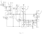
- FIG. 7 is a schematic circuit diagram of a shift register according to an embodiment of the present disclosure.
- FIG. 8 is a timing diagram of two driving clock signal terminals CLKX/CLKX′ of FIG. 7 providing different driving clock signals;
- FIG. 9 is a schematic circuit diagram of a shift register according to an embodiment of the present disclosure.
- FIG. 10 is a timing diagram of two driving clock signal terminals CLKX′/CLKX′′ of FIG. 9 providing different driving clock signals;
- FIG. 11 is a schematic structural diagram of a gate driving circuit according to an embodiment of the present disclosure.
- FIG. 12 is a timing diagram illustrating an operation of the gate driving circuit shown in FIG. 11 .
- the transistor in the present disclosure may be a thin film transistor or a field effect transistor or any other switching device with the same characteristics.
- a transistor generally includes three electrodes, i.e., a gate electrode, a source electrode and a drain electrode, and the source electrode and the drain electrode of the transistor are symmetrical in structure, and may be interchanged as desired.
- the control electrode refers to the gate electrode of the transistor, and one of the first electrode and the second electrode is the source electrode and the other is the drain electrode.
- transistors can be classified into N-type transistors and P-type transistors according to transistor characteristics; when the transistor is an N-type transistor, the transistor would be turned on at a high level voltage, and would be turned off at a low level voltage; when the transistor is a P-type transistor, the transistor would be turned on at a low level voltage, and would be turned off at a high level voltage.
- the “effective level” in the present disclosure refers to a voltage capable of controlling the corresponding transistor to be turned on, and the “non-effective level” refers to a voltage capable of controlling the corresponding transistor to be turned off; accordingly, when the transistor is the N-type transistor, the effective level refers to a high level, and the non-effective level refers to a low level; when the transistor is the P-type transistor, the effective level refers to a low level and the non-effective level refers to a high level, respectively.
- the transistors are exemplified as being N-type transistors. Accordingly, the effective level refers to a high level, and the non-effective level refers to a low level. Those ordinary skilled in the art will appreciate that the transistors in the embodiments described below may be replaced with P-type transistors.
- the display of a frame of picture can be divided into two stages, i.e., a display driving stage and a sensing stage; in the display driving stage, display driving for pixel units in each row in the display panel is completed; in the sensing stage, current drawing (i.e., sensing) for a row of pixel units in the display panel is completed.
- FIG. 1 is a schematic circuit diagram of a pixel circuit in an organic light emitting diode display panel
- FIG. 2 is a timing diagram illustrating an operation of the pixel circuit shown in FIG. 1 , and as shown in FIG. 1 and FIG. 2 , the pixel circuit includes a display switch transistor QTFT (a control electrode thereof is coupled to a gate line G 1 ), a driving transistor DTFT, a sensing switch transistor STFT (a control electrode thereof is coupled to a gate line G 2 ), and a capacitor Cst.
- the pixel circuit When an external compensation is needed to be performed on the pixel circuit, the pixel circuit at least includes following two stages in a working process, that is, a pixel driving stage (including a data voltage writing process) and a pixel sensing stage (including a current reading process).
- a data voltage Vdata in a data line Data needs to be written into the pixel unit; in the pixel sensing stage, a test voltage Vsense needs to be written into the pixel unit through the data line Data, and an electrical signal at the drain electrode of the driving transistor is read to a signal read line Sense through the sensing switch transistor STFT.
- a test voltage Vsense needs to be written into the pixel unit through the data line Data, and an electrical signal at the drain electrode of the driving transistor is read to a signal read line Sense through the sensing switch transistor STFT.
- the gate line G 2 coupled to the gate electrode of the sensing switch transistor STFT Since a duration of the current reading process is longer than that of the data voltage writing process, it is necessary, for the gate line G 2 coupled to the gate electrode of the sensing switch transistor STFT, to output a double pulse signal within a time duration of a frame, and a pulse width corresponding to the current reading process is larger than that corresponding to the data voltage writing process. This requires the gate driving unit to have a function of outputting double pulses having different pulse widths.
- FIG. 3 is a schematic structural diagram of a gate driving unit, and as shown in FIG. 3 , in order to enable the gate driving unit to output a double pulse signal, a first shift register, a second shift register and a signal combining circuit may be used to form the gate driving unit.
- first shift registers in all gate driving units are cascaded
- second shift registers in all gate driving units are cascaded
- the first shift registers are configured to output driving signals for driving display switch transistors in a display driving stage
- the second shift registers are configured to output driving signals for driving sensing switch transistors in a sensing stage
- the signal combining circuit combines the driving signals output by two shift registers located in the same gate driving unit, and outputs a double pulse signal through a signal output terminal OUTPUT to meet driving requirements.
- the technical solution of forming the gate driving unit by two shift registers and the signal combining circuit can satisfy the driving requirement, the structure is complex and the number of transistors required to be arranged is large, which is not favorable for a narrow bezel design.
- the technical solution of the present disclosure provides a shift register, which has a function of outputting double pulses and can meet the driving requirements of a pixel circuit in a pixel driving stage and a pixel sensing stage, and thus the shift register in the present disclosure may be independently used as a gate driving unit.
- the technical solution of the present disclosure can significantly reduce the number of transistors in the gate driving unit, which facilitates to realize a narrow bezel.
- FIG. 4 is a schematic circuit diagram of a shift register provided in an embodiment of the present disclosure, and as shown in FIG. 4 , the shift register includes: a display pre-charge reset circuit 1 , a sensing cascade circuit 2 , a sensing pre-charge reset circuit 3 , a pull-down control circuit 4 and an output circuit, where the sensing cascade circuit 2 and the sensing pre-charge reset circuit 3 are coupled to a sensing cascade node H, the display pre-charge reset circuit 1 , the sensing pre-charge reset circuit 3 , the pull-down control circuit 4 and the output circuit are coupled to a pull-up node PU, and the pull-down control circuit 4 and the output circuit are coupled to a pull-down node PD; the output circuit is coupled to at least one signal output terminal OUTX, and the output circuit includes output sub-circuits 5 in one-to-one correspondence with the at least one signal output terminal OUTX.
- the display pre-charge reset circuit 1 is coupled to a first signal input terminal STU 1 , a display reset signal terminal STD, a first power supply terminal U 1 , and a second power supply terminal U 2 , and is configured to, in a display pre-charge stage, write a first operating voltage in an effective level state provided by the first power supply terminal U 1 into the pull-up node PU in response to a control of a first input signal provided by the first signal input terminal STU 1 ; in a display reset stage, write a second operating voltage in a non-effective level state provided by the second power supply terminal U 2 into the pull-up node PU in response to a control of a first reset signal provided by the display reset signal terminal STD.
- the sensing cascade circuit 2 is coupled to a second signal input terminal STU 2 and a random signal terminal OE, and is configured to write a second input signal in an effective level state provided by the second signal input terminal STU 2 into the sensing cascade node H in response to a control of a random signal provided by the random signal terminal OE during a sensing cascade stage.
- the sensing pre-charge reset circuit 3 is coupled to a first clock signal terminal CLKA, a sensing reset signal terminal TRST and the second power supply terminal U 2 , and is configured to write, in a sensing pre-charge stage, a first clock signal in an effective level state provided by the first clock signal terminal CLKA into the pull-up node PU in response to a control of a voltage of the sensing cascade node H and the first clock signal provided by the first clock signal terminal CLKA; and write, in a sensing reset stage, the second operating voltage in the non-effective level state provided by the second power supply terminal U 2 into the pull-up node PU in response to a control of a second reset signal provided by the sensing reset signal terminal TRST.
- the pull-down control circuit 4 is coupled to the first power supply terminal U 1 and the second power supply terminal U 2 , and is configured to write the second operating voltage in the non-effective level state provided by the second power supply terminal U 2 into the pull-down node PD in response to a control of a voltage of the pull-up node PU when the voltage of the pull-up node PU is in an effective level state; and write the first operating voltage in the effective level state provided by the first power supply terminal U 1 into the pull-down node PD in response to a control of the first operating voltage provided by the first power supply terminal U 1 when the voltage of the pull-up node PU is in a non-effective level state.
- the output sub-circuit 5 is coupled to the pull-up node PU, the pull-down node PD, a corresponding signal output terminal OUTX, a corresponding driving clock signal terminal CLKX, and a corresponding reset power supply terminal UX, and is configured to write a driving clock signal provided by the corresponding driving clock signal terminal CLKX into the corresponding signal output terminal OUTX in response to a control of a voltage of the pull-up node PU in an effective level state in a display output stage and a sensing output stage; and write a reset operating voltage in a non-effective level state provided by the corresponding reset power supply terminal UX into the corresponding signal output terminal OUTX in response to a control of a voltage of the pull-down node PD in an effective level state in the display reset stage and the sensing reset stage.
- the number of signal output terminals OUTX is 1 to 3; accordingly, the number of output sub-circuits 5 is 1 to 3; accordingly, the number of driving clock signal terminals CLKX is 1 to 3, and the number of reset power supply terminals UX is 1 to 3.
- FIG. 4 only illustrates the case of one output sub-circuit 5 , one signal output terminal OUTX, one driving clock signal terminal CLKX, and one reset power supply terminal UX, which does not limit the technical solution of the present disclosure.
- the driving clock signal terminals CLKX corresponding to the multiple output sub-circuits 5 may be the same clock signal terminal or different clock signal terminals; the reset power supply terminals UX corresponding to the output sub-circuits 5 may be the same power supply terminal or different power supply terminals.
- the display pre-charge reset circuit 1 and the sensing pre-charge reset circuit 3 share the pull-down control circuit 4 and the output circuit.
- the gate driving unit including two shift registers and one signal combining circuit the first shift register for outputting the driving signal for driving the display switch transistor in the display driving stage at least includes one display pre-charge reset circuit, one pull-down control circuit, and one output circuit; the second shift register for outputting the driving signal for driving the sensing switch transistor in the sensing stage at least includes one sensing cascade circuit, one sensing pre-charge reset circuit, one pull-down control circuit and one output circuit. Therefore, the gate driving unit including two shift registers and one signal combining circuit at least includes one display pre-charge reset circuit, one sensing cascade circuit, one sensing pre-charge reset circuit, two pull-down control circuits, two output circuits and one signal combining circuit.
- the shift register provided in the embodiment can independently constitute a gate driving unit, and thus the gate driving unit in the present disclosure includes one display pre-charge reset circuit 1 , one sensing cascade circuit 2 , one sensing pre-charge reset circuit 3 , one pull-down control circuit 4 , and one output circuit.
- the shift register provided by the embodiment can save one pull-down control circuit and one output circuit by sharing the pull-down control circuit and the output circuit; meanwhile, the shift register provided by the embodiment does not need to be provided with the signal combining circuit.
- the gate driving unit including the shift register provided by the present disclosure can save one pull-down control circuit, one output circuit and the signal combining circuit, and therefore, in practical applications, the shift register provided by the embodiment can reduce the number of thin film transistors (TFTs) in the gate driving unit, which is beneficial to the implementation of a narrow bezel.
- TFTs thin film transistors
- FIG. 5 is a schematic circuit diagram of a shift register provided in an embodiment of the present disclosure, and the shift register shown in FIG. 5 is a specific scheme based on the shift register shown in FIG. 4 .
- the display pre-charge reset circuit 1 includes: a first transistor M 1 and a second transistor M 2 .
- a control electrode of the first transistor M 1 is coupled to the first signal input terminal STU 1 , a first electrode of the first transistor M 1 is coupled to the first power supply terminal U 1 , and a second electrode of the first transistor M 1 is coupled to the pull-up node PU.
- the first power supply terminal U 1 is configured to provide the first operating voltage in the effective level state, for example, the first operating voltage is a high level voltage VDD.
- a control electrode of the second transistor M 2 is coupled to the display reset signal terminal STD, a first electrode of the second transistor M 2 is coupled to the pull-up node PU, and a second electrode of the second transistor M 2 is coupled to the second power supply terminal U 2 .
- the second power supply terminal U 2 is configured to provide the second operating voltage in the non-effective level state, for example, the second operating voltage is a low level voltage VGL 1 .
- the sensing cascade circuit 2 includes: a third transistor M 3 ; a control electrode of the third transistor M 3 is coupled to the random signal terminal OE, a first electrode of the third transistor M 3 is coupled to the second signal input terminal STU 2 , and a second electrode of the third transistor M 3 is coupled to the sensing cascade node H.
- the random signal terminal OE may be a random signal terminal implemented based on an FPGA (Field Programmable Gate Array), and configured to provide a random signal.
- the shift register further includes: a first capacitor C 1 , where a first terminal of the first capacitor C 1 is coupled to the sensing cascade node H, and a second terminal of the first capacitor C 2 is coupled to the second power supply terminal U 2 .
- the first capacitor C 1 is configured to maintain the voltage of the sensing cascade node H stable when the third transistor M 3 is turned off.
- the sensing pre-charge reset circuit 3 includes: a fourth transistor M 4 , a fifth transistor M 5 , and a sixth transistor M 6 .
- a control electrode of the fourth transistor M 4 is coupled to the sensing cascade node H, a first electrode of the fourth transistor M 4 is coupled to the first clock signal terminal CLKA, and a second electrode of the fourth transistor M 4 is coupled to a sensing pre-charge node N.
- a control electrode of the fifth transistor M 5 is coupled to the first clock signal terminal CLKA, a first electrode of the fifth transistor M 5 is coupled to the sensing pre-charge node N, and a second electrode of the fifth transistor M 5 is coupled to the pull-up node PU.
- signal terminals to which the control electrode of the fifth transistor M 5 and the first electrode of the fourth transistor M 4 are coupled may be different signal terminals, and the embodiment is not limited to the way in which the control electrode of the fifth transistor M 5 and the first electrode of the fourth transistor M 4 are coupled to the same first clock signal terminal CLKA.
- a control electrode of the sixth transistor M 6 is coupled to the sensing reset signal terminal TRST, a first electrode of the sixth transistor M 6 is coupled to the pull-up node PU, and a second electrode of the sixth transistor M 6 is coupled to the second power supply terminal U 2 .
- the pull-down control circuit 4 includes: a seventh transistor M 7 , an eighth transistor M 8 , a ninth transistor M 9 , and a tenth transistor M 10 .
- a control electrode of the seventh transistor M 7 is coupled to the first power supply terminal U 1 , a first electrode of the seventh transistor M 7 is coupled to the first power supply terminal U 1 , and a second electrode of the seventh transistor M 7 is coupled to a first electrode of the eighth transistor M 8 .
- a control electrode of the eighth transistor M 8 is coupled to the first electrode of the eighth transistor M 8 , and a second electrode of the eighth transistor M 8 is coupled to the pull-down node PD.
- a control electrode of the ninth transistor M 9 is coupled to the pull-up node PU, a first electrode of the ninth transistor M 9 is coupled to the pull-down node PD, and a second electrode of the ninth transistor M 9 is coupled to a first electrode of the tenth transistor M 10 .
- a control electrode of the tenth transistor M 10 is coupled to the pull-up node PU, and a second electrode of the tenth transistor M 10 is coupled to the second power supply terminal U 2 .
- the pull-down control circuit 4 may include only the seventh transistor M 7 and the ninth transistor M 9 , in such case, the second electrode of the seventh transistor is coupled to the pull-down node PD, and the second electrode of the ninth transistor M 9 is coupled to the second power supply terminal U 2 .
- an impedance between the first power supply terminal U 1 and the second power supply terminal U 2 can be increased and a current between the first power supply terminal U 1 and the second power supply terminal U 2 can be effectively reduced by the seventh transistor M 7 and the eighth transistor M 8 which are cascaded, and the ninth transistor M 9 and the tenth transistor M 10 which are cascaded, and thus a phenomenon that wiring of the second power supply terminal U 2 is easily blown in an overcurrent state lasting for a long time can be effectively prevented.
- the current flowing through the ninth transistor M 9 is 12 ⁇ A
- the current flowing through the ninth transistor M 9 is 6 ⁇ A.
- the transistor (TFT) in the embodiment is a depletion type TFT, a threshold voltage Vth thereof is liable to be in a negative value state, and therefore, before the display pre-charge stage, since the control electrode of the ninth transistor M 9 is in the non-effective level state (e.g. at the low level voltage VGL 1 ), the second electrode of the ninth transistor M 9 is in the non-effective level state (e.g. at the low level voltage VGL 1 ), the first electrode of the ninth transistor M 9 is in the effective level state (e.g.
- the ninth transistor M 9 is in a leakage state, but in the embodiment, in the pull-down control circuit 4 , the seventh transistor M 7 is cascaded to the eighth transistor M 8 , the ninth transistor M 9 is cascaded to the tenth transistor M 10 , thereby increasing the impedance between the first power supply terminal U 1 (a power source supplying the high level voltage VDD) and the second power supply terminal U 2 (a power source supplying the low level voltage VGL 1 ), thereby effectively preventing the leakage of the transistor.
- the shift register further includes: a first noise reduction circuit 6 coupled to the pull-up node PU and the pull-down node PD, and the first noise reduction circuit 6 is coupled to the second power supply terminal U 2 , and is configured to write, when the voltage of the pull-up node PU is in the non-effective level state, in response to a control of the voltage of the pull-down node PD, the second operating voltage in the non-effective level state, which is provided by the second power supply terminal U 2 , into the pull-up node PU, so as to release noise from the pull-up node PU, and maintain stability of the voltage at the pull-up node PU.
- the first noise reduction circuit 6 includes: an eleventh transistor M 11 , where a control electrode of the eleventh transistor M 11 is coupled to the pull-down node PD, a first electrode of the eleventh transistor M 11 is coupled to the pull-up node PU, and a second electrode of the eleventh transistor M 11 is coupled to the second power supply terminal U 2 .
- the output sub-circuit 5 includes: a twelfth transistor M 12 and a thirteenth transistor M 13 .
- a control electrode of the twelfth transistor M 12 is coupled to the pull-up node PU, a first electrode of the twelfth transistor M 12 is coupled to the driving clock signal terminal CLKX corresponding to the output sub-circuit 5 , and a second electrode of the twelfth transistor M 12 is coupled to the signal output terminal OUTX corresponding to the output sub-circuit 5 .
- a control electrode of the thirteenth transistor M 13 is coupled to the pull-down node PD, a first electrode of the thirteenth transistor M 13 is coupled to the signal output terminal OUTX corresponding to the output sub-circuit 5 , and a second electrode of the thirteenth transistor M 13 is coupled to the reset power supply terminal UX corresponding to the output sub-circuit.
- one signal output terminal OUTX is included, accordingly, one output sub-circuit 5 is included, one reset signal terminal UX is included, and one driving clock signal terminal CLKX is included.
- the shift register further includes: a second capacitor C 2 , a first terminal of the second capacitor C 2 is coupled to the pull-up node PU, and a second terminal of the second capacitor C 2 is coupled to the signal output terminal OUTX.
- the second capacitor C 2 can be configured to ensure that the voltage of the pull-up node PU is always in the effective level state during the display output stage and the sensing output stage.
- the second capacitor C 2 may be a parasitic capacitor of the twelfth transistor M 12 or an external capacitor.
- the shift register further includes: a second noise reduction circuit 7 , where the second noise reduction circuit 7 is coupled to the pull-down node PD and the sensing cascade node H, and the second noise reduction circuit 7 is coupled to the first clock signal terminal CLKA and the second power supply terminal U 2 , and is configured to write, in the sensing pre-charge stage, in response to a control of the voltage of the sensing cascade node H and the first clock signal provided by the first clock signal terminal CLKA, the second operating voltage in the non-effective level state provided by the second power supply terminal U 2 into the pull-down node PD, so as to perform noise reduction processing on the pull-down node PD, so as to maintain the voltage at the pull-down node PD stable.
- a second noise reduction circuit 7 is coupled to the pull-down node PD and the sensing cascade node H
- the second noise reduction circuit 7 is coupled to the first clock signal terminal CLKA and the second power supply terminal U 2 , and is configured to write, in the sensing pre-charge stage,
- the second noise reduction circuit 7 includes a fourteenth transistor M 14 and a fifteenth transistor M 15 , where a control electrode of the fourteenth transistor M 14 is coupled to the first clock signal terminal CLKA, a first electrode of the fourteenth transistor M 14 is coupled to the pull-down node PD, a second electrode of the fourteenth transistor M 14 is coupled to a first electrode of the fifteenth transistor M 15 , a control electrode of the fifteenth transistor M 15 is coupled to the sensing cascade node H, and a second electrode of the fifteenth transistor M 15 is coupled to the second power supply terminal U 2 .
- the shift register further includes: a third noise reduction circuit 8 , where the third noise reduction circuit 8 is coupled to the pull-down node PD, and the third noise reduction circuit 8 is coupled to the first signal input terminal STU 1 and the second power supply terminal U 2 , and is configured to write, in the display pre-charge stage, the second operating voltage in the non-effective level state provided by the second power supply terminal U 2 into the pull-down node PD in response to a control of the first input signal provided by the first signal input terminal STU 1 , so as to perform noise reduction processing on the pull-down node PD, so as to maintain the voltage at the pull-down node PD stable.
- a third noise reduction circuit 8 is coupled to the pull-down node PD
- the third noise reduction circuit 8 is coupled to the first signal input terminal STU 1 and the second power supply terminal U 2 , and is configured to write, in the display pre-charge stage, the second operating voltage in the non-effective level state provided by the second power supply terminal U 2 into the pull-down node PD
- the third noise reduction circuit 8 includes a sixteenth transistor M 16 , a control electrode of the sixteenth transistor M 16 is coupled to the first signal input terminal STU 1 , a first electrode of the sixteenth transistor M 16 is coupled to the pull-down node PD, and a second electrode of the sixteenth transistor M 16 is coupled to the second power supply terminal U 2 .
- the operation of the shift register shown in FIG. 5 will be described in detail below with reference to the accompanying drawings.
- the first operating voltage provided by the first power supply terminal is a direct-current (DC) high level voltage VDD
- the second operating voltage provided by the second power supply terminal is a low level voltage VGL 1
- the reset operating voltage provided by the reset power supply terminal UX is a low level voltage VGL 2
- VGL 1 is lower than VGL 2
- VGL 1 and VGL 2 are both negative.
- FIG. 6 is a timing diagram showing the operation of the shift register shown in FIG. 5 , and as shown in FIG. 5 and FIG. 6 , the operation of the shift register includes the following seven stages, i.e., t 0 to t 6 .
- the first input signal provided by the first signal input terminal STU 1 is in a low level state
- the second input signal provided by the second signal input terminal STU 2 is in a low level state
- the first reset signal provided by the display reset signal terminal STD is in a low level state
- the first clock signal provided by the first clock signal terminal CLKA is in a low level state
- the random signal provided by the random signal terminal OE is in a high level state
- the second reset signal provided by the sensing reset signal terminal TRST is in a high level state
- the first operating voltage VDD provided by the first power supply terminal U 1 is in a high level state
- the second operating voltage VGL 1 provided by the second power supply terminal U 2 is in a low level state
- the driving clock signal provided by the driving clock signal terminal CLKX corresponding to the output sub-circuit 5 is in a low level state
- the reset operating voltage VGL 2 provided by the reset signal terminal UX is in a low level state.
- the third transistor M 3 is turned on under the control of the random signal (being a high level signal) provided by the random signal terminal OE, the second input signal (being a low level signal) provided by the second signal input terminal STU 2 is written into the sensing cascade node H through the third transistor M 3 being turned on, and the voltage of the sensing cascade node H is in a low level state.
- the fourth transistor M 4 is turned off under the control of the voltage (being a low level voltage) of the sensing cascade node H. Since the first clock signal is in the low level state at this time, the fifth transistor M 5 is turned off.
- the sixth transistor M 6 Since the sixth transistor M 6 is turned on under the control of the second reset signal (being a high level signal) provided by the sensing reset signal terminal TRST, the second operating voltage VGL 1 provided by the second power supply terminal U 2 is written into the pull-up node PU through the sixth transistor M 6 being turned on, and the pull-up node PU is in a low level state.
- both the first transistor M 1 and the second transistor M 2 are turned off.
- the ninth transistor M 9 , the tenth transistor M 10 , and the twelfth transistor M 12 are all turned off, meanwhile, in the pull-down control circuit 4 , under the control of the first operating voltage VDD provided by the first power supply terminal U 1 , the seventh transistor M 7 and the eighth transistor M 8 are turned on, the first operating voltage VDD provided by the first power supply terminal U 1 is written into the pull-down node PD through the seventh transistor M 7 and the eighth transistor M 8 which are turned on, and the voltage of the pull-down node PD is in a high level state.
- the thirteenth transistor M 13 is turned on under the control of the voltage of the pull-down node PD (being a high level voltage), and the reset operating voltage VGL 2 provided by the reset power supply terminal UX corresponding to the output sub-circuit 5 is written into the corresponding signal output terminal OUTX through the thirteenth transistor M 13 being turned on, that is, the signal output terminal OUTX outputs a low level signal.
- the first input signal provided by the first signal input terminal STU 1 is in a high level state
- the second input signal provided by the second signal input terminal STU 2 is first in a low level state and is switched to the high level state after a period of time
- the first reset signal provided by the display reset signal terminal STD is in the low level state
- the first clock signal provided by the first clock signal terminal CLKA is in the low level state
- the random signal provided by the random signal terminal OE is in the low level state
- the second reset signal provided by the sensing reset signal terminal TRST is in the low level state
- the driving clock signal provided by the driving clock signal terminal CLKX is in the low level state.
- both the third transistor M 3 and the sixth transistor M 6 are turned off, the sensing cascade node H is in a floating state, and the voltage of the sensing cascade node H maintains in the high level state of a previous stage. It should be noted that, since the third transistor M 3 is turned off, the second input signal provided by the second signal input terminal STU 2 does not affect the voltage of the sensing cascade node H, whether the second input signal is in a high level state or a low level state.
- the first capacitor C 1 in the embodiment can maintain the voltage of the sensing cascade node H stable after the sensing cascade stage t 0 ends and when the sensing cascade node H is in the floating state; since the first clock signal is still in the low level state, the fifth transistor M 5 maintains turned off.
- the first transistor M 1 is turned on and the second transistor M 2 is turned off, the first operating voltage VDD provided by the first power supply terminal U 1 can be written into the pull-up node PU through the first transistor M 1 being turned on, and the voltage of the pull-up node PU is in a high level state.
- the ninth transistor M 9 , the tenth transistor M 10 and the twelfth transistor M 12 are turned on under the control of the voltage of the pull-up node PU, the second operating voltage VGL 1 provided by the second power supply terminal U 2 is written into the pull-down node PD through the ninth transistor M 9 and the tenth transistor M 10 which are turned on, at this time, the seventh transistor M 7 and the eighth transistor M 8 are equivalent to a resistor, and the voltage of the pull-down node PD is in a low level state, and thus the eleventh transistor M 11 and the thirteenth transistor M 13 are turned off.
- the driving clock signal provided by the driving clock signal terminal CLKX is written into the corresponding signal output terminal OUTX through the twelfth transistor M 12 being turned on, but since the driving clock signal is in a low level state, the corresponding signal output terminal OUTX outputs a low level signal.
- the sixteenth transistor M 16 is turned on under the control of the first input signal (being at the high level) provided by the first signal input terminal STU 1 , and the second operating voltage VGL 1 provided by the second power supply terminal U 2 is written into the pull-down node PD through the sixteenth transistor M 16 being turned on, so that the noise reduction processing is performed on the pull-down node PD to maintain the voltage at the pull-down node PD stable.
- the first input signal provided by the first signal input terminal STU 1 is in a low level state
- the second input signal provided by the second signal input terminal STU 2 is first in a high level state and is switched to a low level state after a period of time
- the first reset signal provided by the display reset signal terminal STD is in a low level state
- the first clock signal provided by the first clock signal terminal CLKA is in a low level state
- the random signal provided by the random signal terminal OE is in a low level state
- the second reset signal provided by the sensing reset signal terminal TRST is in a low level state
- the driving clock signal provided by the driving clock signal terminal CLKX is first in a high level state and is switched to a low level state after a period of time.
- the third transistor M 3 and the sixth transistor M 6 are both turned off, the sensing cascade node H is in the floating state, and the voltage of the sensing cascade node H maintains in the high level state of a previous stage (the second input signal does not affect the voltage of the sensing cascade node H); since the first clock signal provided by the first clock signal terminal CLKA is still in the low level state, the fifth transistor M 5 maintains turned off.
- the first transistor M 1 and the second transistor M 2 are both turned off, the pull-up node PU is in the floating state and maintains in the high level state of a previous stage, the ninth transistor M 9 , the tenth transistor M 10 and the twelfth transistor M 12 maintain to be turned on, the pull-down node PD maintains in the low level state, the eleventh transistor M 11 and the thirteenth transistor M 13 are both turned off, and the driving clock signal provided by the driving clock signal terminal CLKX is written into the corresponding signal output terminal OUTX through the twelfth transistor M 12 being turned on.
- the driving clock signal provided by the driving clock signal terminal CLKX is switched from the low level state to the high level state, and the signal output terminal OUT outputs the high level signal. Meanwhile, under bootstrap action of the second capacitor C 2 , the voltage of the pull-up node PU is pulled up to a higher level state.
- the voltage corresponding to each clock signal is VGH when it is in the high level state and VGL (approximately 0V) when it is in the low level state
- VGH approximately 0V
- the driving clock signal is switched from the high level state to the low level state, and then the signal output terminal OUTX outputs a low level signal; meanwhile, under bootstrap action of the second capacitor C 2 , the voltage of the pull-up node PU decreases to the level at the initial time of the display driving stage t 2 , i.e., to VGH, and the pull-up node PU is still in a high level state.
- the first input signal provided by the first signal input terminal STU 1 is in a low level state
- the second input signal provided by the second signal input terminal STU 2 is in a low level state
- the first reset signal provided by the display reset signal terminal STD is in a high level state
- the first clock signal provided by the first clock signal terminal CLKA is in a low level state
- the random signal provided by the random signal terminal OE is in a low level state
- the second reset signal provided by the sensing reset signal terminal TRST is in a low level state
- the driving clock signal provided by the driving clock signal terminal CLKX is first in a low level state and is switched to a high level state after a period of time.
- the third transistor M 3 and the sixth transistor M 6 are both turned off, the sensing cascade node H is in the floating state, and the voltage of the sensing cascade node H maintains in the high level state of a previous stage (the second input signal does not affect the voltage of the sensing cascade node H); since the first clock signal provided by the first clock signal terminal CLKA is still in the low level state, the fifth transistor M 5 maintains turned off.
- the first transistor M 1 Since the first input signal provided from the first signal input terminal STU 1 is in the low level state, the first transistor M 1 is turned off, and since the first reset signal provided by the display reset signal terminal STD is in the high level state, the second transistor M 2 is turned on, the second operating voltage VGL 1 provided by the second power supply terminal U 2 is written into the pull-up node PU through the second transistor M 2 being turned on, and the voltage of the pull-up node PU is pulled down to a low level state.
- the ninth transistor M 9 , the tenth transistor M 10 , and the twelfth transistor M 12 are all in turned off. Since the twelfth transistor M 12 is turned off, the driving clock signal provided by the driving clock signal terminal CLKX cannot be written into the signal output terminal OUTX, and thus, the voltage of the signal output terminal OUTX is not affected.
- the seventh transistor M 7 and the eighth transistor M 8 are turned on under the control of the first operating voltage VDD provided by the first power supply terminal U 1 , the first operating voltage VDD provided by the first power supply terminal U 1 is written into the pull-down node PD through the seventh transistor M 7 and the eighth transistor M 8 which are turned on, the voltage of the pull-down node PD becomes in a high level state, at this time, both the eleventh transistor M 11 and the thirteenth transistor M 13 are turned on, the second operating voltage VGL 1 provided by the second power supply terminal U 2 is written into the pull-up node PU through the eleventh transistor M 11 being turned on, so as to reduce the noise the pull-up node PU, and meanwhile, the reset operating voltage VGL 2 provided by the reset power supply terminal UX is written into the signal output terminal OUTX through the thirteenth transistor M 13 being turned on, that is, the signal output terminal OUTX outputs a low level signal.
- the first input signal provided by the first signal input terminal STU 1 is in a low level state
- the second input signal provided by the second signal input terminal STU 2 is in a low level state
- the first reset signal provided by the display reset signal terminal STD is in a low level state
- the first clock signal provided by the first clock signal terminal CLKA is in a high level state
- the random signal provided by the random signal terminal OE is in a low level state
- the second reset signal provided by the sensing reset signal terminal TRST is in a low level state
- the driving clock signal provided by the driving clock signal terminal CLKX is in a low level state.
- the third transistor M 3 and the sixth transistor M 6 are both turned off, the sensing cascade node H is in the floating state, the voltage of the sensing cascade node H maintains in the high level state of a previous stage (the second input signal does not affect the voltage of the sensing cascade node H), and accordingly the fourth transistor M 4 maintains turned on.
- the fifth transistor M 5 since the first clock signal provided by the first clock signal terminal CLKA is in the high level state, the fifth transistor M 5 is turned on, the first clock signal in the high level state is written into the pull-up node PU through the fourth transistor M 4 and fifth transistor M 5 , which are turned on, in sequence, and the voltage of the pull-up node PU is in a high level state.
- both the first input signal provided by the first signal input terminal STU 1 and the first reset signal provided by the display reset signal terminal STD are in the low level state, both the first transistor M 1 and the second transistor M 2 are turned off.
- the ninth transistor M 9 , the tenth transistor M 10 , and the twelfth transistor M 12 are all turned on, the second operating voltage VGL 1 provided by the second power supply terminal U 2 is written into the pull-down node PD through the ninth transistor M 9 and the tenth transistor M 10 which are turned on, at this time, the seventh transistor M 7 and the eighth transistor M 8 are equivalent to a resistor, the voltage of the pull-down node PD is in a low level state, and the eleventh transistor M 11 and the thirteenth transistor M 13 are both turned off.
- the driving clock signal provided by the driving clock signal terminal CLKX is written into the corresponding signal output terminal OUTX through the twelfth transistor M 12 being turned on, but since the driving clock signal is in the low level state, the signal output terminal OUTX outputs a low level signal.
- both the fourteenth transistor M 14 and the fifteenth transistor M 15 are turned on, and the second operating voltage VGL 1 in the non-effective level state (low level state) provided by the second power supply terminal U 2 is written into the pull-down node PD, thereby reducing noise of the pull-down node PD to maintain the voltage in the pull-down node PD stable.
- the first input signal provided by the first signal input terminal STU 1 is in a low level state
- the second input signal provided by the second signal input terminal STU 2 is in a low level state
- the first reset signal provided by the display reset signal terminal STD is in a low level state
- the first clock signal provided by the first clock signal terminal CLKA is in a low level state
- the random signal provided by the random signal terminal OE is in a low level state
- the second reset signal provided by the sensing reset signal terminal TRST is in a low level state
- the driving clock signal provided by the driving clock signal terminal CLKX is first in a high level state first and is switched to a low level state after a period of time.
- the third transistor M 3 and the sixth transistor M 6 are both turned off, the sensing cascade node H is in the floating state, the voltage of the sensing cascade node H maintains in the high level state of a previous stage (the second input signal does not affect the voltage of the sensing cascade node H), and the fourth transistor M 4 maintains turned on; since the first clock signal provided by the first clock signal terminal CLKA is in the low level state, the fifth transistor M 5 is turned off, and the first clock signal does not affect the voltage of the pull-up node PU.
- the first transistor M 1 and the second transistor M 2 are both turned off, the pull-up node PU is in the floating state and maintains in the high level state of a previous stage, the ninth transistor M 9 , the tenth transistor M 10 and the twelfth transistor M 12 are maintained to be turned on, the pull-down node PD is maintained in the low level state, the eleventh transistor M 11 and the thirteenth transistor 13 are maintained to be turned off, and the driving clock signal provided by the driving clock signal terminal CLKX is written into the corresponding signal output terminal OUTX through the twelfth transistor M 12 being turned on.
- the driving clock signal is switched from the low level state to the high level state, and the signal output terminal OUTX outputs a high level signal. Meanwhile, under bootstrap action of the second capacitor C 2 , the voltage of the pull-up node PU is pulled up to a higher level state.
- the voltage corresponding to each clock signal is VGH when it is at a high level and VGL (approximately 0V) when it is at a low level
- the voltage of the pull-up node PU is approximately VGH during the sensing pre-charge stage t 4 , and the voltage of the pull-up node PU can be pulled up to approximately 2VGH at the initial time of the sensing driving stage t 5 .
- the driving clock signal is switched from the high level state to a low level state, and then the signal output terminal OUTX outputs a low level signal; meanwhile, under bootstrap action of the second capacitor C 2 , the voltage of the pull-up node PU decreases to the level at the initial time of the sensing driving period t 5 , i.e., to VGH, and at this time, the pull-up node PU is still in the high level state.
- the first input signal provided by the first signal input terminal STU 1 is in a low level state
- the second input signal provided by the second signal input terminal STU 2 is in a low level state
- the first reset signal provided by the display reset signal terminal STD is in a low level state
- the first clock signal provided by the first clock signal terminal CLKA is in a low level state
- the random signal provided by the random signal terminal OE is in a high level state
- the second reset signal provided by the sensing reset signal terminal TRST is in a high level state
- the driving clock signal provided by the driving clock signal terminal CLKX is in a low level state.
- the third transistor M 3 and the sixth transistor M 6 are both turned on, the second input signal provided by the second signal input terminal STU 2 is written into the sensing cascade node H through the third transistor M 3 being turned on, the voltage of the sensing cascade node H is in a low level state, and the fourth transistor M 4 is turned off, so that the sensing cascade node H is totally reset. Since the first clock signal is in the low level state, the fifth transistor M 5 is turned off.
- the sixth transistor M 6 Since the sixth transistor M 6 is turned on, the second operating voltage VGL 1 provided by the second power supply terminal U 2 is written into the pull-up node PU through the second transistor M 2 being turned on, and the voltage of the pull-up node PU is in a low level state, so that the pull-up node PU is totally reset.
- both the first transistor M 1 and the second transistor M 2 are turned off.
- the ninth transistor M 9 , the tenth transistor M 10 , and the twelfth transistor M 12 are all turned off; in the pull-down control circuit 4 , the first operating voltage VDD provided by the first power supply terminal U 1 is written into the pull-down node PD through the seventh transistor M 7 and the eighth transistor M 8 which are turned on, the voltage of the pull-down node PD is in a high level state, at this time, the eleventh transistor M 11 and the thirteenth transistor M 13 are turned on, the second operating voltage VGL 1 provided by the second power supply terminal U 2 is written into the pull-up node PU through the eleventh transistor M 11 to reduce noise of the pull-up node PU, and the reset operating voltage VGL 2 provided by the reset power supply terminal UX is written into the signal output terminal OUTX through the thirteenth transistor M 13 , that is, the signal output terminal OUTX outputs a low level signal.
- the shift register can respectively output high level (effective level) signals in the display driving stage and the sensing stage of a frame to meet the driving requirements of pixel units in a corresponding row.
- the voltage of the pull-up node PU is maintained at the low level (non-effective level) during a period from an end of the display reset stage t 3 to a start of the sensing pre-charge stage t 4 .
- the pull-down control circuit 4 and the eleventh transistor M 11 can form a positive feedback loop to strengthen the voltage at the pull-up node PU.
- the pull-down control circuit 4 controls the voltage of the pull-down node PD to be in the high level state, the eleventh transistor M 11 is turned on, and the second operating voltage VGL 1 is written into the pull-up node PU through the eleventh transistor M 11 , so as to strengthen that the voltage of the pull-up node PU is in the low level state (the voltage is VGL 1 ), thereby achieving a purpose of reducing noise.
- FIG. 7 is another schematic circuit diagram of a shift register according to an embodiment of the present disclosure, and as shown in FIG. 7 , different from the foregoing embodiment, in the present embodiment, the number of output sub-circuits is two, and accordingly, the number of signal output terminals is two, the number of driving clock signal terminals is two, and the number of reset power supply terminals is two.
- the number of output sub-circuits is two, and accordingly, the number of signal output terminals is two, the number of driving clock signal terminals is two, and the number of reset power supply terminals is two.
- the two output sub-circuits are a first output sub-circuit 5 and a second output sub-circuit 5 ′
- the two signal output terminals are a signal output terminal OUTX and a signal output terminal OUTX′
- the two driving clock signal terminals are a driving clock signal terminal CLKX and a driving clock signal terminal CLKX′
- the two reset power supply terminals are a reset power supply terminal UX and a reset power supply terminal UX′, respectively.
- the first output sub-circuit 5 includes a twelfth transistor M 12 and a thirteenth transistor M 13 , and for the specific connection relationship of the twelfth transistor M 12 and the thirteenth transistor M 13 , reference may be made to the description of the twelfth transistor and the thirteenth transistor in the foregoing embodiment, and details are not repeated here;
- the second output sub-circuit 5 ′ includes a transistor M 12 ′ and a transistor M 13 ′, similarly, for the specific connection relationship of the transistor M 12 ′ and the transistor M 13 ′, reference may be made to the description of the twelfth transistor and the thirteenth transistor in the foregoing embodiment, and details are not repeated here.
- the twelfth transistor M 12 in the first output sub-circuit 5 and the transistor M 12 ′ in the second output sub-circuit 5 ′ are turned on or off at the same time, and the thirteenth transistor M 13 in the first output sub-circuit 5 and the transistor M 13 ′ in the second output sub-circuit 5 ′ are turned on or off at the same time.
- the driving clock signal provided by the driving clock signal terminal CLKX coupled to the first output sub-circuit 5 and the driving clock signal provided by the driving clock signal terminal CLKX′ coupled to the second output sub-circuit 5 ′ may be the same or different.
- the driving clock signal terminal CLKX coupled to the first output sub-circuit 5 provides the same driving clock signal as the driving clock signal terminal CLKX′ coupled to the second output sub-circuit 5 ′.
- one of the two signal output terminals OUTX/OUTX′ e.g., the signal output terminal OUTX in FIG. 7
- the other e.g., the signal output terminal OUTX′ in FIG. 7
- the signal output terminal for providing the cascade signal is separated from the signal output terminal for providing the driving signal, so that the load on the signal output terminal for providing the driving signal can be reduced, and the stability of the driving signal output by the shift register to the corresponding row of gate line can be ensured.
- the driving clock signal terminal CLKX coupled to the first output sub-circuit 5 provides a driving clock signal different from that provided by the driving clock signal terminal CLKX′ coupled to the second output sub-circuit 5 ′.
- FIG. 8 is a timing diagram of different driving clock signals provided by the two driving clock signal terminals CLKX/CLKX′ of FIG. 7 , and as shown in FIG. 8 , the two driving clock signal terminals CLKX/CLKX′ provide the same driving clock signal in the display driving stage, but providing different driving clock signals in the sensing stage; the driving clock signal provided by the driving clock signal terminal CLKX corresponds to the driving signal required by the gate line G 2 coupled to the control electrode of the sensing switch transistor STFT in the pixel unit (see FIG. 1 ), and the driving clock signal provided by the driving clock signal terminal CLKX′ corresponds to the driving signal required by the gate line G 1 coupled to the control electrode of the display switch transistor QTFT (see FIG. 1 ).
- one of the two signal output terminals OUTX/OUTX′ (e.g., the signal output terminal OUTX in FIG. 7 ) is configured to provide a cascade signal to another shift register in the gate driving circuit and simultaneously provide a driving signal to the gate line G 2 coupled to the control electrode of the sensing switch transistor STFT in the pixel unit of the corresponding row
- the other e.g., the signal output terminal OUTX′ in FIG. 7
- the other is configured to provide a driving signal to the gate line G 1 coupled to the control electrode of the display switch transistor QTFT in the pixel unit of the corresponding row.
- one shift register can simultaneously provide driving signals for two gate lines coupled to pixel units, so that no additional shift register needs to be provided for the gate line G 1 coupled to the control electrode of the display switch transistor QTFT, the number of shift registers in the display panel can be effectively reduced, and a design of narrow bezel is facilitated.
- the reset power supply terminal UX coupled to the first output sub-circuit 5 and the reset power supply terminal UX′ coupled to the second output sub-circuit 5 ′ may be a same power supply terminal or different power supply terminals.
- the reset power supply terminal UX coupled to the first output sub-circuit 5 is the second power supply terminal U 2
- the reset power supply terminal UX′ coupled to the second output sub-circuit 5 ′ is a third power supply terminal U 3
- the second operating voltage VGL 1 provided by the second power supply terminal U 2 is lower than a third operating voltage VGL 2 provided by the third power supply terminal U 3
- VGL 1 and VGL 2 are both negative.
- the reset power supply terminal UX coupled to the first output sub-circuit 5 and the reset power supply terminal UX′ coupled to the second output sub-circuit 5 ′ are both the third power supply terminal U 3 , and the third power supply terminal U 3 is configured to provide the third operating voltage VGL 2 .
- a first terminal of the second capacitor C 2 is coupled to the pull-up node PU, and a second terminal of the second capacitor C 2 is coupled to the signal output terminal OUTX′ corresponding to the second output sub-circuit 5 ′.
- FIG. 9 is another schematic circuit diagram of a shift register according to an embodiment of the present disclosure, and as shown in FIG. 9 , different from the foregoing embodiment, in the present embodiment, the number of output sub-circuits is three, and accordingly, the number of signal output terminals is three, the number of driving clock signal terminals is three, and the number of reset power supply terminals is three.
- the number of output sub-circuits is three, and accordingly, the number of signal output terminals is three, the number of driving clock signal terminals is three, and the number of reset power supply terminals is three.
- the three output sub-circuits are a first output sub-circuit 5 , a second output sub-circuit 5 ′ and a third output sub-circuit 5 ′′
- the three signal output terminals are a signal output terminal OUTX, a signal output terminal OUTX′ and a signal output terminal OUTX′′
- the three driving clock signal terminals are a driving clock signal terminal CLKX, a driving clock signal terminal CLKX′ and a driving clock signal terminal CLKX′′
- the three reset power supply terminals are a reset power supply terminal UX, a reset power supply terminal UX′ and a reset power supply terminal UX′′, respectively.
- the first output sub-circuit 5 includes a twelfth transistor M 12 and a thirteenth transistor M 13 , and for the specific connection relationship of the twelfth transistor M 12 and the thirteenth transistor M 13 , reference may be made to the description of the twelfth transistor and the thirteenth transistor in the foregoing embodiment, and details are not repeated here;
- the second output sub-circuit 5 ′ includes a transistor M 12 ′ and a transistor M 13 ′, similarly, for the specific connection relationship of the transistor M 12 ′ and the transistor M 13 ′, reference may be made to the description of the twelfth transistor and the thirteenth transistor in the foregoing embodiment, and details are not repeated here;
- the third output sub-circuit 5 ′′ includes a transistor M 12 ′′ and a transistor M 13 ′′, similarly, for the specific connection relationship between the transistor M 12 ′′ and the transistor M 13 ′′, reference may be made to the description of the twelfth transistor and the thirteenth transistor in the foregoing embodiment, and details are
- the twelfth transistor M 12 in the first output sub-circuit 5 , the transistor M 12 ′ in the second output sub-circuit 5 ′ and the transistor M 12 ′′ in the third output sub-circuit 5 ′′ are turned on or off at the same time, and the thirteenth transistor M 13 in the first output sub-circuit 5 , the transistor M 13 ′ in the second output sub-circuit 5 ′ and the transistor M 13 ′′ in the third output sub-circuit 5 ′′ are turned on or off at the same time.
- one of the three signal output terminals OUTX/OUTX′/OUTX′′ (e.g., the signal output terminal OUTX in FIG. 9 ) is configured to provide a cascade signal to another shift register in the gate driving circuit, and the other two signal output terminals OUTX′/OUTX′′ in FIG. 9 are configured to provide driving signals to the gate line G 1 coupled to the control electrode of the display switch transistor QTFT and the gate line G 2 coupled to the control electrode of the sensing switch transistor STFT in the pixel unit of the corresponding row, respectively.
- the driving clock signal terminal CLKX corresponding to the signal output terminal OUTX, the driving clock signal terminal CLKX′ corresponding to the signal output terminal OUTX′, and the driving clock signal terminal CLKX′′ corresponding to the signal output terminal OUTX′′ may be the same or different.
- the operation timing when the driving clock signal terminal CLKX′ corresponding to the signal output terminal OUTX′ and the driving clock signal terminal CLKX′′ corresponding to the signal output terminal OUTX′′ provide different driving clock signals is shown in FIG. 10 .
- the operation timings of the three driving clock signal terminals CLKX, CLKX′, and CLKX′′ may all be the same, i.e., the three driving clock signal terminals CLKX, CLKX′, and CLKX′′ provide the same driving clock signal.
- one of the three signal output terminals OUTX/OUTX′/OUTX′′ is configured to provide a driving signal to the gate line G 2 coupled to the control electrode of the sensing switch transistor STFT in the pixel unit of the corresponding row, and the other two signal output terminals are configured to provide cascade signals to other shift registers in the gate driving circuit.
- the reset power supply terminal UX coupled to the first output sub-circuit 5 may be the same power supply terminal or different power supply terminals.
- the reset power supply terminal UX coupled to the first output sub-circuit 5 is the second power supply terminal U 2
- the reset power supply terminal UX′ coupled to the second output sub-circuit 5 ′ and the reset power supply terminal UX′′ coupled to the third output sub-circuit 5 ′′ are both the third power supply terminal U 3
- the second operating voltage VGL 1 provided by the second power supply terminal U 2 is lower than the third operating voltage VGL 2 provided by the third power supply terminal U 3
- both VGL 1 and VGL 2 are negative.
- the reset power supply terminal UX coupled to the first output sub-circuit 5 , the reset power supply terminal UX′ coupled to the second output sub-circuit 5 ′, and the reset power supply terminal UX′′ coupled to the third output sub-circuit 5 ′′ are all the third power supply terminal U 3 , and the third power supply terminal U 3 is configured to provide the third operating voltage VGL 2 .
- a first terminal of the second capacitor C 2 is coupled to the pull-up node PU, and a second terminal of the second capacitor C 2 is coupled to the signal output terminal OUTX′ corresponding to the second output sub-circuit 5 ′.
- the shift register further includes a third capacitor C 3 , a first terminal of the third capacitor C 3 is coupled to the pull-up node PU, and a second terminal of the third capacitor C 3 is coupled to the signal output terminal OUTX′′ corresponding to the third output sub-circuit 5 ′′.
- FIG. 11 is a schematic structural diagram of a gate driving circuit according to an embodiment of the present disclosure, and as shown in FIG. 11 , the gate driving circuit includes: N shift registers A 1 /A 2 /A 3 /A 4 . . . /AN which are cascaded and the shift registers A 1 /A 2 /A 3 /A 4 . . . /AN each adopt the shift registers provided by any one of the above embodiments.
- first signal input terminals STU 1 of the shift registers A 1 /A 2 at the first and second stages are coupled to a frame start signal input terminal STV 1
- the first signal input terminal STU 1 of the shift register at the i th stage is coupled to one signal output terminal of the shift register at the (i ⁇ 2) th stage, where i is greater than or equal to 3 and less than or equal to N, and i is a positive integer.
- the second signal input terminal STU 2 of the shift register at the first stage is coupled to a sensing start signal input terminal STV 2
- the second signal input terminal STU 2 of the shift register at the j th stage is coupled to one signal output terminal of the shift register at the (j ⁇ 1) th stage, where j is greater than or equal to 2 and less than or equal to N, and j is a positive integer.
- Display reset signal terminals STD of the shift registers from the (N ⁇ 2) th stage to the N th stage are coupled to a frame reset signal terminal (not shown), the display reset signal terminal STD at the k th stage is coupled to one signal output terminal of the shift register at the (k+3) th stage, where k is greater than or equal to 1 and less than or equal to N ⁇ 3, and k is a positive integer.
- the first clock signal terminal CLKA of each shift register is coupled to the first clock signal line CLKA
- the random signal terminal OE of each shift register is coupled to the random signal line OE
- the sensing reset signal terminal TRST of each shift register is coupled to the sensing reset signal line TRST.
- the gate driving circuit is provided with four clock signal lines CKX 1 /CKX 2 /CKX 3 /CKX 4 .
- the driving clock signal terminal CLKX of the shift register at the (4m ⁇ 3) th stage is coupled to the driving clock signal line CKX 1
- the driving clock signal terminal CLKX of the shift register at the (4m ⁇ 2) th stage is coupled to the second driving clock signal line CKX 2
- the driving clock signal terminal CLKX of the shift register at the (4m ⁇ 1) th stage is coupled to the third driving clock signal line CKX 3
- the driving clock signal terminal CLKX of the shift register at the 4m th stage is coupled to the fourth driving clock signal line CKX 4
- m is greater than or equal to 1 and less than or equal to N
- m is a positive integer.
- the driving clock signal terminal CLKX, the driving clock signal terminal CLKX′, and the driving clock signal terminal CLKX′′ of the shift register at the same stage are coupled to the same clock signal line.
- each of the shift registers A 1 /A 2 /A 3 /A 4 is coupled to three corresponding signal output terminals CR 1 /CR 2 /OUT, which are respectively a first cascade signal output terminal CR 1 (for providing a cascade signal to another shift register in the gate driving circuit), a second cascade signal output terminal CR 2 (for providing a cascade signal to another shift register in the gate driving circuit), and a first driving signal output terminal OUT (for providing a driving signal to the gate line G 2 coupled to the control electrode of the sensing switch transistor STFT in the pixel unit of the corresponding row);
- the first signal input terminal STU 1 of the shift register at the i th stage is coupled to the first cascade signal output terminal CR 1 of the shift register at the (i ⁇ 2) th stage;
- the second signal input terminal STU 2 of the shift register at the j th stage is coupled to the second cascade signal output terminal CR 2 of the shift register at the (j ⁇ ) th stage;
- FIG. 12 is a timing diagram illustrating the operation of the gate driving circuit shown in FIG. 11 , as shown in FIG. 12 , in the display driving stage of each frame, the shift registers A 1 /A 2 /A 3 /A 4 sequentially outputs driving signals to the gate lines Gate 1 /Gate 2 /Gate 3 /Gate 4 of corresponding rows, so as to drive the display panel to display an image; in the sensing stage of each frame, only the shift register at one stage outputs a driving signal to sense a current of a display element or driving transistor in the pixel unit of the corresponding row for an external compensation; each row of pixel units is externally compensated frame by frame.
- an overlap ratio of the driving clock signals supplied by the driving clock signal lines CKX 1 , CKX 2 , CKX 3 and CKX 4 an overlap ratio of the driving signals of adjacent rows of gate lines can be controlled.
- An embodiment of the present disclosure further provides a display device, including the gate driving circuit provided in the above embodiment, and for details, reference is made to the description in the above embodiment, and details are not repeated here.
Landscapes
- Engineering & Computer Science (AREA)
- Physics & Mathematics (AREA)
- Computer Hardware Design (AREA)
- General Physics & Mathematics (AREA)
- Theoretical Computer Science (AREA)
- Control Of Indicators Other Than Cathode Ray Tubes (AREA)
- Shift Register Type Memory (AREA)
Abstract
Description
Claims (15)
Applications Claiming Priority (3)
| Application Number | Priority Date | Filing Date | Title |
|---|---|---|---|
| CN201910458518.2 | 2019-05-29 | ||
| CN201910458518.2A CN110136653B (en) | 2019-05-29 | 2019-05-29 | Shift register, grid drive circuit and display device |
| PCT/CN2020/092022 WO2020238833A1 (en) | 2019-05-29 | 2020-05-25 | Shift register, gate drive circuit and display apparatus |
Publications (2)
| Publication Number | Publication Date |
|---|---|
| US20220005400A1 US20220005400A1 (en) | 2022-01-06 |
| US11568791B2 true US11568791B2 (en) | 2023-01-31 |
Family
ID=67582651
Family Applications (1)
| Application Number | Title | Priority Date | Filing Date |
|---|---|---|---|
| US17/279,478 Active US11568791B2 (en) | 2019-05-29 | 2020-05-25 | Shift register, gate driving circuit and display device |
Country Status (3)
| Country | Link |
|---|---|
| US (1) | US11568791B2 (en) |
| CN (1) | CN110136653B (en) |
| WO (1) | WO2020238833A1 (en) |
Cited By (1)
| Publication number | Priority date | Publication date | Assignee | Title |
|---|---|---|---|---|
| US12236824B2 (en) * | 2021-01-28 | 2025-02-25 | Boe Technology Group Co., Ltd. | Gate driving circuit, method of driving gate driving circuit, and display panel |
Families Citing this family (21)
| Publication number | Priority date | Publication date | Assignee | Title |
|---|---|---|---|---|
| CN110136653B (en) * | 2019-05-29 | 2022-05-13 | 合肥京东方卓印科技有限公司 | Shift register, grid drive circuit and display device |
| CN112447133B (en) | 2019-08-30 | 2022-05-20 | 京东方科技集团股份有限公司 | Shift register and driving method thereof, gate drive circuit and display panel |
| CN110956918B (en) * | 2019-12-17 | 2023-06-09 | 京东方科技集团股份有限公司 | Shifting register, driving method thereof, substrate and electronic equipment |
| CN111081180B (en) | 2020-01-17 | 2022-06-14 | 合肥鑫晟光电科技有限公司 | Array substrate, detection method thereof and display device |
| CN111179808B (en) | 2020-01-22 | 2023-04-18 | 合肥京东方卓印科技有限公司 | Shift register, gate driving circuit, display device and gate driving method |
| CN111261108A (en) * | 2020-02-11 | 2020-06-09 | 深圳市华星光电半导体显示技术有限公司 | Gate drive circuit |
| CN111292664B (en) * | 2020-02-20 | 2022-08-09 | 合肥京东方卓印科技有限公司 | Gate drive circuit, display panel and display method thereof |
| CN111599315B (en) | 2020-06-19 | 2021-11-16 | 京东方科技集团股份有限公司 | Shift register, grid driving circuit and driving method thereof |
| CN114120923B (en) * | 2020-08-26 | 2022-11-25 | 深圳市柔宇科技股份有限公司 | Scanning driving circuit and display panel |
| CN113035258B (en) * | 2021-03-09 | 2024-08-09 | 京东方科技集团股份有限公司 | Shift register, gate drive circuit and display panel |
| CN113257186B (en) | 2021-05-28 | 2022-09-20 | 合肥京东方卓印科技有限公司 | Scanning driving circuit, display panel and display device |
| CN113362772B (en) * | 2021-06-29 | 2022-11-18 | 合肥京东方卓印科技有限公司 | Display substrate, display panel and display device |
| CN114627946A (en) * | 2022-03-11 | 2022-06-14 | 合肥鑫晟光电科技有限公司 | Shift register, gate drive circuit and display device |
| CN114677964B (en) * | 2022-04-12 | 2024-04-05 | Tcl华星光电技术有限公司 | Shift register, grid driving circuit and display panel |
| KR20240087174A (en) * | 2022-12-12 | 2024-06-19 | 엘지디스플레이 주식회사 | Gate driver and display device using the same |
| KR20240091380A (en) * | 2022-12-13 | 2024-06-21 | 삼성디스플레이 주식회사 | Scan signal driver and display device including the same |
| CN116189589B (en) * | 2023-01-17 | 2026-01-30 | 福州京东方光电科技有限公司 | Shift register, gate drive circuit, display substrate and display device |
| GB2639776A (en) * | 2023-03-20 | 2025-10-01 | Boe Technology Group Co Ltd | Shift register unit, gate drive circuit, and display panel |
| CN118865879A (en) * | 2023-04-26 | 2024-10-29 | 京东方科技集团股份有限公司 | Driving circuit, driving method, display substrate and display device |
| CN118016020A (en) * | 2024-03-06 | 2024-05-10 | 深圳市华星光电半导体显示技术有限公司 | A gate drive circuit |
| CN121002558A (en) * | 2024-03-19 | 2025-11-21 | 京东方科技集团股份有限公司 | Gate driving circuit, display substrate and display device |
Citations (20)
| Publication number | Priority date | Publication date | Assignee | Title |
|---|---|---|---|---|
| US20130100007A1 (en) * | 2010-07-13 | 2013-04-25 | Sharp Kabushiki Kaisha | Shift register and display device having the same |
| US20140093028A1 (en) * | 2012-04-13 | 2014-04-03 | Boe Technology Group Co., Ltd. | Shift register unit and driving method thereof, shift register and display apparatus |
| US20150036784A1 (en) * | 2013-04-01 | 2015-02-05 | BOE Technology Group Co., Ltd. a corporation | Shift register unit, shift register and display apparatus |
| CN105185294A (en) | 2015-10-23 | 2015-12-23 | 京东方科技集团股份有限公司 | Shift register unit and a drive method, a shift register and a display device thereof |
| US20160117963A1 (en) | 2014-10-28 | 2016-04-28 | Samsung Display Co., Ltd. | Scan sense driver and display device including the same |
| CN105741742A (en) * | 2016-05-09 | 2016-07-06 | 京东方科技集团股份有限公司 | Shifting register unit, grid driving circuit and driving method thereof |
| CN106683634A (en) | 2017-03-30 | 2017-05-17 | 京东方科技集团股份有限公司 | Shifting register, GOA circuit, driving method thereof and display device |
| CN107464539A (en) * | 2017-09-21 | 2017-12-12 | 京东方科技集团股份有限公司 | Shift register cell, drive device, display device and driving method |
| CN107993607A (en) | 2018-01-23 | 2018-05-04 | 京东方科技集团股份有限公司 | Drive element of the grid and its driving method, gate driving circuit and display device |
| US20180174503A1 (en) * | 2016-12-19 | 2018-06-21 | Lg Display Co., Ltd. | Gate driving circuit |
| CN108648718A (en) | 2018-08-01 | 2018-10-12 | 京东方科技集团股份有限公司 | Shift register cell and its driving method, gate driving circuit and display device |
| CN108877627A (en) | 2018-07-13 | 2018-11-23 | 京东方科技集团股份有限公司 | Shift register cell and driving method, gate driving circuit, display device |
| CN109346007A (en) | 2018-11-26 | 2019-02-15 | 合肥鑫晟光电科技有限公司 | Shift register unit, gate driving circuit, display device and driving method |
| US20190103049A1 (en) * | 2017-09-29 | 2019-04-04 | Lg Display Co., Ltd. | Gate driver and flat panel display device including the same |
| CN109658865A (en) | 2019-02-25 | 2019-04-19 | 合肥京东方卓印科技有限公司 | Shift register cell and its driving method, gate driving circuit, display device |
| CN109698006A (en) | 2019-02-19 | 2019-04-30 | 京东方科技集团股份有限公司 | Shift register and its driving method, cascade driving circuit and display device |
| CN109935269A (en) | 2018-05-31 | 2019-06-25 | 京东方科技集团股份有限公司 | Shift register unit and driving method thereof, gate driving circuit and display device |
| CN109949749A (en) | 2018-08-01 | 2019-06-28 | 京东方科技集团股份有限公司 | Shift register, gate driving circuit, display device and grid drive method |
| CN110136653A (en) | 2019-05-29 | 2019-08-16 | 合肥京东方卓印科技有限公司 | Shift register, grid drive circuit and display device |
| US20200135115A1 (en) * | 2018-10-30 | 2020-04-30 | Lg Display Co., Ltd. | Gate driver, organic light emitting display device including the same, and method for operating the same |
Family Cites Families (5)
| Publication number | Priority date | Publication date | Assignee | Title |
|---|---|---|---|---|
| US8223112B2 (en) * | 2007-12-27 | 2012-07-17 | Sharp Kabushiki Kaisha | Shift register receiving all-on signal and display device |
| CN106023943A (en) * | 2016-08-02 | 2016-10-12 | 京东方科技集团股份有限公司 | Shifting register and drive method thereof, grid drive circuit and display device |
| CN108932933B (en) * | 2017-05-27 | 2020-01-21 | 京东方科技集团股份有限公司 | Shift register, gate drive circuit, display device |
| CN107564458A (en) * | 2017-10-27 | 2018-01-09 | 京东方科技集团股份有限公司 | Shift register cell, driving method, gate driving circuit and display device |
| CN108777128A (en) * | 2018-05-31 | 2018-11-09 | 京东方科技集团股份有限公司 | Shift register and its driving method, gate driving circuit and display device |
-
2019
- 2019-05-29 CN CN201910458518.2A patent/CN110136653B/en active Active
-
2020
- 2020-05-25 WO PCT/CN2020/092022 patent/WO2020238833A1/en not_active Ceased
- 2020-05-25 US US17/279,478 patent/US11568791B2/en active Active
Patent Citations (20)
| Publication number | Priority date | Publication date | Assignee | Title |
|---|---|---|---|---|
| US20130100007A1 (en) * | 2010-07-13 | 2013-04-25 | Sharp Kabushiki Kaisha | Shift register and display device having the same |
| US20140093028A1 (en) * | 2012-04-13 | 2014-04-03 | Boe Technology Group Co., Ltd. | Shift register unit and driving method thereof, shift register and display apparatus |
| US20150036784A1 (en) * | 2013-04-01 | 2015-02-05 | BOE Technology Group Co., Ltd. a corporation | Shift register unit, shift register and display apparatus |
| US20160117963A1 (en) | 2014-10-28 | 2016-04-28 | Samsung Display Co., Ltd. | Scan sense driver and display device including the same |
| CN105185294A (en) | 2015-10-23 | 2015-12-23 | 京东方科技集团股份有限公司 | Shift register unit and a drive method, a shift register and a display device thereof |
| CN105741742A (en) * | 2016-05-09 | 2016-07-06 | 京东方科技集团股份有限公司 | Shifting register unit, grid driving circuit and driving method thereof |
| US20180174503A1 (en) * | 2016-12-19 | 2018-06-21 | Lg Display Co., Ltd. | Gate driving circuit |
| CN106683634A (en) | 2017-03-30 | 2017-05-17 | 京东方科技集团股份有限公司 | Shifting register, GOA circuit, driving method thereof and display device |
| CN107464539A (en) * | 2017-09-21 | 2017-12-12 | 京东方科技集团股份有限公司 | Shift register cell, drive device, display device and driving method |
| US20190103049A1 (en) * | 2017-09-29 | 2019-04-04 | Lg Display Co., Ltd. | Gate driver and flat panel display device including the same |
| CN107993607A (en) | 2018-01-23 | 2018-05-04 | 京东方科技集团股份有限公司 | Drive element of the grid and its driving method, gate driving circuit and display device |
| CN109935269A (en) | 2018-05-31 | 2019-06-25 | 京东方科技集团股份有限公司 | Shift register unit and driving method thereof, gate driving circuit and display device |
| CN108877627A (en) | 2018-07-13 | 2018-11-23 | 京东方科技集团股份有限公司 | Shift register cell and driving method, gate driving circuit, display device |
| CN108648718A (en) | 2018-08-01 | 2018-10-12 | 京东方科技集团股份有限公司 | Shift register cell and its driving method, gate driving circuit and display device |
| CN109949749A (en) | 2018-08-01 | 2019-06-28 | 京东方科技集团股份有限公司 | Shift register, gate driving circuit, display device and grid drive method |
| US20200135115A1 (en) * | 2018-10-30 | 2020-04-30 | Lg Display Co., Ltd. | Gate driver, organic light emitting display device including the same, and method for operating the same |
| CN109346007A (en) | 2018-11-26 | 2019-02-15 | 合肥鑫晟光电科技有限公司 | Shift register unit, gate driving circuit, display device and driving method |
| CN109698006A (en) | 2019-02-19 | 2019-04-30 | 京东方科技集团股份有限公司 | Shift register and its driving method, cascade driving circuit and display device |
| CN109658865A (en) | 2019-02-25 | 2019-04-19 | 合肥京东方卓印科技有限公司 | Shift register cell and its driving method, gate driving circuit, display device |
| CN110136653A (en) | 2019-05-29 | 2019-08-16 | 合肥京东方卓印科技有限公司 | Shift register, grid drive circuit and display device |
Non-Patent Citations (1)
| Title |
|---|
| First Office Action dated Sep. 3, 2021 for application No. CN201910458518.2 with English translation attached. |
Cited By (1)
| Publication number | Priority date | Publication date | Assignee | Title |
|---|---|---|---|---|
| US12236824B2 (en) * | 2021-01-28 | 2025-02-25 | Boe Technology Group Co., Ltd. | Gate driving circuit, method of driving gate driving circuit, and display panel |
Also Published As
| Publication number | Publication date |
|---|---|
| CN110136653B (en) | 2022-05-13 |
| WO2020238833A1 (en) | 2020-12-03 |
| CN110136653A (en) | 2019-08-16 |
| US20220005400A1 (en) | 2022-01-06 |
Similar Documents
| Publication | Publication Date | Title |
|---|---|---|
| US11568791B2 (en) | Shift register, gate driving circuit and display device | |
| US11081061B2 (en) | Shift register, gate driving circuit, display device and gate driving method | |
| US11545093B2 (en) | Shift register, gate driving circuit, display device and gate driving method | |
| US12100357B2 (en) | Shift register, gate drive circuit and driving method therefor | |
| US10950321B2 (en) | Shift register, gate driving circuit, display panel and display device | |
| US8964932B2 (en) | Shift register, gate driving circuit and display | |
| US10593279B2 (en) | Display device, gate driving circuit and gate driving unit | |
| US11024234B2 (en) | Signal combination circuit, gate driving unit, gate driving circuit and display device | |
| US11295645B2 (en) | Shift register and driving method thereof, gate driving circuit and display apparatus | |
| US12293719B2 (en) | Shift register, driving circuit and display substrate | |
| US20230107029A1 (en) | Display substrate, display device and display driving method | |
| US12154502B2 (en) | Pixel circuit, driving method thereof, display substrate and display apparatus | |
| US11127355B2 (en) | Shift register, gate driving circuit, display device and driving method | |
| US10490156B2 (en) | Shift register, gate driving circuit and display panel | |
| JPWO2010050262A1 (en) | Shift register circuit, display device, and shift register circuit driving method | |
| US11250784B2 (en) | Shift register, driving method thereof, gate drive circuit, array substrate and display device | |
| US20210335196A1 (en) | Shift Register Unit, Driving Method, Gate Driver on Array and Display Device | |
| US11238769B2 (en) | Shift register unit, driving method, gate driving circuit and display device | |
| WO2025223057A1 (en) | Shift register, light-emission driving circuit, and display apparatus | |
| CN119028257A (en) | Shift register unit and driving method thereof, gate driving circuit, and display device | |
| US11328785B2 (en) | Shift register, gate driving circuit and gate driving method | |
| CN117672325A (en) | Shift register unit, gate drive circuit, display panel and display device | |
| US20250232718A1 (en) | Shift register unit, gate driving circuit and display panel | |
| CN118629338A (en) | Shift register unit and driving method thereof, display driving circuit, and display device |
Legal Events
| Date | Code | Title | Description |
|---|---|---|---|
| FEPP | Fee payment procedure |
Free format text: ENTITY STATUS SET TO UNDISCOUNTED (ORIGINAL EVENT CODE: BIG.); ENTITY STATUS OF PATENT OWNER: LARGE ENTITY |
|
| AS | Assignment |
Owner name: BOE TECHNOLOGY GROUP CO., LTD., CHINA Free format text: ASSIGNMENT OF ASSIGNORS INTEREST;ASSIGNORS:FENG, XUEHUAN;LI, YONGQIAN;REEL/FRAME:055772/0692 Effective date: 20201125 Owner name: HEFEI BOE JOINT TECHNOLOGY CO., LTD., CHINA Free format text: ASSIGNMENT OF ASSIGNORS INTEREST;ASSIGNORS:FENG, XUEHUAN;LI, YONGQIAN;REEL/FRAME:055772/0692 Effective date: 20201125 |
|
| STPP | Information on status: patent application and granting procedure in general |
Free format text: DOCKETED NEW CASE - READY FOR EXAMINATION |
|
| STPP | Information on status: patent application and granting procedure in general |
Free format text: NON FINAL ACTION MAILED |
|
| STPP | Information on status: patent application and granting procedure in general |
Free format text: RESPONSE TO NON-FINAL OFFICE ACTION ENTERED AND FORWARDED TO EXAMINER |
|
| STPP | Information on status: patent application and granting procedure in general |
Free format text: NOTICE OF ALLOWANCE MAILED -- APPLICATION RECEIVED IN OFFICE OF PUBLICATIONS |
|
| STPP | Information on status: patent application and granting procedure in general |
Free format text: PUBLICATIONS -- ISSUE FEE PAYMENT RECEIVED |
|
| STPP | Information on status: patent application and granting procedure in general |
Free format text: PUBLICATIONS -- ISSUE FEE PAYMENT VERIFIED |
|
| STCF | Information on status: patent grant |
Free format text: PATENTED CASE |