US11534755B2 - Micro-channel device and manufacturing method thereof and micro-fluidic system - Google Patents
Micro-channel device and manufacturing method thereof and micro-fluidic system Download PDFInfo
- Publication number
- US11534755B2 US11534755B2 US16/755,911 US201916755911A US11534755B2 US 11534755 B2 US11534755 B2 US 11534755B2 US 201916755911 A US201916755911 A US 201916755911A US 11534755 B2 US11534755 B2 US 11534755B2
- Authority
- US
- United States
- Prior art keywords
- micro
- rails
- layer
- semiconductor layer
- type semiconductor
- Prior art date
- Legal status (The legal status is an assumption and is not a legal conclusion. Google has not performed a legal analysis and makes no representation as to the accuracy of the status listed.)
- Active, expires
Links
- 238000004519 manufacturing process Methods 0.000 title claims description 9
- 239000004065 semiconductor Substances 0.000 claims abstract description 109
- 239000000758 substrate Substances 0.000 claims description 20
- 239000000463 material Substances 0.000 claims description 11
- 239000004020 conductor Substances 0.000 claims description 7
- 238000004544 sputter deposition Methods 0.000 claims description 5
- 238000000034 method Methods 0.000 description 18
- -1 polydimethylsiloxane Polymers 0.000 description 11
- 239000004698 Polyethylene Substances 0.000 description 8
- 239000000523 sample Substances 0.000 description 8
- 239000012530 fluid Substances 0.000 description 6
- 239000002131 composite material Substances 0.000 description 5
- 239000000126 substance Substances 0.000 description 5
- 229920000642 polymer Polymers 0.000 description 4
- 238000007796 conventional method Methods 0.000 description 3
- 229920001577 copolymer Polymers 0.000 description 3
- 238000005516 engineering process Methods 0.000 description 3
- 238000005530 etching Methods 0.000 description 3
- 230000001788 irregular Effects 0.000 description 3
- 229910052751 metal Inorganic materials 0.000 description 3
- 239000002184 metal Substances 0.000 description 3
- 238000000059 patterning Methods 0.000 description 3
- 108090000623 proteins and genes Proteins 0.000 description 3
- XOLBLPGZBRYERU-UHFFFAOYSA-N tin dioxide Chemical compound O=[Sn]=O XOLBLPGZBRYERU-UHFFFAOYSA-N 0.000 description 3
- 102000053602 DNA Human genes 0.000 description 2
- 108020004414 DNA Proteins 0.000 description 2
- 229920006169 Perfluoroelastomer Polymers 0.000 description 2
- 239000004696 Poly ether ether ketone Substances 0.000 description 2
- 238000004458 analytical method Methods 0.000 description 2
- 238000000231 atomic layer deposition Methods 0.000 description 2
- CXKCTMHTOKXKQT-UHFFFAOYSA-N cadmium oxide Inorganic materials [Cd]=O CXKCTMHTOKXKQT-UHFFFAOYSA-N 0.000 description 2
- CFEAAQFZALKQPA-UHFFFAOYSA-N cadmium(2+);oxygen(2-) Chemical compound [O-2].[Cd+2] CFEAAQFZALKQPA-UHFFFAOYSA-N 0.000 description 2
- 238000000151 deposition Methods 0.000 description 2
- 238000000609 electron-beam lithography Methods 0.000 description 2
- 239000010931 gold Substances 0.000 description 2
- 229910003437 indium oxide Inorganic materials 0.000 description 2
- PJXISJQVUVHSOJ-UHFFFAOYSA-N indium(iii) oxide Chemical compound [O-2].[O-2].[O-2].[In+3].[In+3] PJXISJQVUVHSOJ-UHFFFAOYSA-N 0.000 description 2
- 238000000623 plasma-assisted chemical vapour deposition Methods 0.000 description 2
- 229920001748 polybutylene Polymers 0.000 description 2
- 229920002530 polyetherether ketone Polymers 0.000 description 2
- 102000004169 proteins and genes Human genes 0.000 description 2
- 229920002477 rna polymer Polymers 0.000 description 2
- IXURVUHDDXFYDR-UHFFFAOYSA-N 1-[4-(difluoromethoxy)-3-(oxolan-3-yloxy)phenyl]-3-methylbutan-1-one Chemical compound CC(C)CC(=O)C1=CC=C(OC(F)F)C(OC2COCC2)=C1 IXURVUHDDXFYDR-UHFFFAOYSA-N 0.000 description 1
- JVERADGGGBYHNP-UHFFFAOYSA-N 5-phenylbenzene-1,2,3,4-tetracarboxylic acid Chemical compound OC(=O)C1=C(C(O)=O)C(C(=O)O)=CC(C=2C=CC=CC=2)=C1C(O)=O JVERADGGGBYHNP-UHFFFAOYSA-N 0.000 description 1
- NIXOWILDQLNWCW-UHFFFAOYSA-M Acrylate Chemical compound [O-]C(=O)C=C NIXOWILDQLNWCW-UHFFFAOYSA-M 0.000 description 1
- JBRZTFJDHDCESZ-UHFFFAOYSA-N AsGa Chemical compound [As]#[Ga] JBRZTFJDHDCESZ-UHFFFAOYSA-N 0.000 description 1
- RYGMFSIKBFXOCR-UHFFFAOYSA-N Copper Chemical compound [Cu] RYGMFSIKBFXOCR-UHFFFAOYSA-N 0.000 description 1
- 229920000089 Cyclic olefin copolymer Polymers 0.000 description 1
- 238000000018 DNA microarray Methods 0.000 description 1
- 229920002943 EPDM rubber Polymers 0.000 description 1
- 239000004593 Epoxy Substances 0.000 description 1
- 229920000181 Ethylene propylene rubber Polymers 0.000 description 1
- KRHYYFGTRYWZRS-UHFFFAOYSA-M Fluoride anion Chemical compound [F-] KRHYYFGTRYWZRS-UHFFFAOYSA-M 0.000 description 1
- 239000004812 Fluorinated ethylene propylene Substances 0.000 description 1
- 229910001218 Gallium arsenide Inorganic materials 0.000 description 1
- 239000002033 PVDF binder Substances 0.000 description 1
- 229920001774 Perfluoroether Polymers 0.000 description 1
- 239000004952 Polyamide Substances 0.000 description 1
- 239000004642 Polyimide Substances 0.000 description 1
- 229920002367 Polyisobutene Polymers 0.000 description 1
- 239000004743 Polypropylene Substances 0.000 description 1
- 239000004793 Polystyrene Substances 0.000 description 1
- VYPSYNLAJGMNEJ-UHFFFAOYSA-N Silicium dioxide Chemical compound O=[Si]=O VYPSYNLAJGMNEJ-UHFFFAOYSA-N 0.000 description 1
- BQCADISMDOOEFD-UHFFFAOYSA-N Silver Chemical compound [Ag] BQCADISMDOOEFD-UHFFFAOYSA-N 0.000 description 1
- 229920002125 Sokalan® Polymers 0.000 description 1
- 102000002262 Thromboplastin Human genes 0.000 description 1
- 108010000499 Thromboplastin Proteins 0.000 description 1
- 241000700605 Viruses Species 0.000 description 1
- XLOMVQKBTHCTTD-UHFFFAOYSA-N Zinc monoxide Chemical compound [Zn]=O XLOMVQKBTHCTTD-UHFFFAOYSA-N 0.000 description 1
- 229910003107 Zn2SnO4 Inorganic materials 0.000 description 1
- GTDPSWPPOUPBNX-UHFFFAOYSA-N ac1mqpva Chemical compound CC12C(=O)OC(=O)C1(C)C1(C)C2(C)C(=O)OC1=O GTDPSWPPOUPBNX-UHFFFAOYSA-N 0.000 description 1
- 239000004676 acrylonitrile butadiene styrene Substances 0.000 description 1
- 229920000122 acrylonitrile butadiene styrene Polymers 0.000 description 1
- 229910052782 aluminium Inorganic materials 0.000 description 1
- XAGFODPZIPBFFR-UHFFFAOYSA-N aluminium Chemical compound [Al] XAGFODPZIPBFFR-UHFFFAOYSA-N 0.000 description 1
- 239000000427 antigen Substances 0.000 description 1
- 102000036639 antigens Human genes 0.000 description 1
- 108091007433 antigens Proteins 0.000 description 1
- 238000012742 biochemical analysis Methods 0.000 description 1
- 238000010256 biochemical assay Methods 0.000 description 1
- IEJHYFOJNUCIBD-UHFFFAOYSA-N cadmium(2+) indium(3+) oxygen(2-) Chemical compound [O-2].[Cd+2].[In+3] IEJHYFOJNUCIBD-UHFFFAOYSA-N 0.000 description 1
- BEQNOZDXPONEMR-UHFFFAOYSA-N cadmium;oxotin Chemical compound [Cd].[Sn]=O BEQNOZDXPONEMR-UHFFFAOYSA-N 0.000 description 1
- 150000001720 carbohydrates Chemical class 0.000 description 1
- 210000004027 cell Anatomy 0.000 description 1
- 239000000919 ceramic Substances 0.000 description 1
- 238000006243 chemical reaction Methods 0.000 description 1
- 238000005229 chemical vapour deposition Methods 0.000 description 1
- 210000000349 chromosome Anatomy 0.000 description 1
- 239000011248 coating agent Substances 0.000 description 1
- 238000000576 coating method Methods 0.000 description 1
- 229910052802 copper Inorganic materials 0.000 description 1
- 239000010949 copper Substances 0.000 description 1
- 238000005260 corrosion Methods 0.000 description 1
- 230000007797 corrosion Effects 0.000 description 1
- 238000001514 detection method Methods 0.000 description 1
- 235000014113 dietary fatty acids Nutrition 0.000 description 1
- 239000004205 dimethyl polysiloxane Substances 0.000 description 1
- 238000001312 dry etching Methods 0.000 description 1
- 229920001971 elastomer Polymers 0.000 description 1
- 239000000806 elastomer Substances 0.000 description 1
- 238000005566 electron beam evaporation Methods 0.000 description 1
- 238000001962 electrophoresis Methods 0.000 description 1
- 230000002708 enhancing effect Effects 0.000 description 1
- 238000001704 evaporation Methods 0.000 description 1
- 230000008020 evaporation Effects 0.000 description 1
- 239000000194 fatty acid Substances 0.000 description 1
- 229930195729 fatty acid Natural products 0.000 description 1
- 150000004665 fatty acids Chemical class 0.000 description 1
- NBVXSUQYWXRMNV-UHFFFAOYSA-N fluoromethane Chemical compound FC NBVXSUQYWXRMNV-UHFFFAOYSA-N 0.000 description 1
- 229920002313 fluoropolymer Polymers 0.000 description 1
- UQSQSQZYBQSBJZ-UHFFFAOYSA-N fluorosulfonic acid Chemical compound OS(F)(=O)=O UQSQSQZYBQSBJZ-UHFFFAOYSA-N 0.000 description 1
- 239000011521 glass Substances 0.000 description 1
- PCHJSUWPFVWCPO-UHFFFAOYSA-N gold Chemical compound [Au] PCHJSUWPFVWCPO-UHFFFAOYSA-N 0.000 description 1
- 229910052737 gold Inorganic materials 0.000 description 1
- 229910052738 indium Inorganic materials 0.000 description 1
- APFVFJFRJDLVQX-UHFFFAOYSA-N indium atom Chemical compound [In] APFVFJFRJDLVQX-UHFFFAOYSA-N 0.000 description 1
- 229910001410 inorganic ion Inorganic materials 0.000 description 1
- 239000000543 intermediate Substances 0.000 description 1
- 238000002032 lab-on-a-chip Methods 0.000 description 1
- 150000002632 lipids Chemical class 0.000 description 1
- 239000007788 liquid Substances 0.000 description 1
- 238000001755 magnetron sputter deposition Methods 0.000 description 1
- 230000007246 mechanism Effects 0.000 description 1
- 239000002207 metabolite Substances 0.000 description 1
- 239000002905 metal composite material Substances 0.000 description 1
- 150000002739 metals Chemical class 0.000 description 1
- 239000000203 mixture Substances 0.000 description 1
- 238000001127 nanoimprint lithography Methods 0.000 description 1
- 230000001537 neural effect Effects 0.000 description 1
- 239000002858 neurotransmitter agent Substances 0.000 description 1
- TWNQGVIAIRXVLR-UHFFFAOYSA-N oxo(oxoalumanyloxy)alumane Chemical compound O=[Al]O[Al]=O TWNQGVIAIRXVLR-UHFFFAOYSA-N 0.000 description 1
- KYKLWYKWCAYAJY-UHFFFAOYSA-N oxotin;zinc Chemical compound [Zn].[Sn]=O KYKLWYKWCAYAJY-UHFFFAOYSA-N 0.000 description 1
- RVTZCBVAJQQJTK-UHFFFAOYSA-N oxygen(2-);zirconium(4+) Chemical compound [O-2].[O-2].[Zr+4] RVTZCBVAJQQJTK-UHFFFAOYSA-N 0.000 description 1
- 229920009441 perflouroethylene propylene Polymers 0.000 description 1
- 239000010702 perfluoropolyether Substances 0.000 description 1
- 238000000206 photolithography Methods 0.000 description 1
- 229920002493 poly(chlorotrifluoroethylene) Polymers 0.000 description 1
- 229920000435 poly(dimethylsiloxane) Polymers 0.000 description 1
- 229920003229 poly(methyl methacrylate) Polymers 0.000 description 1
- 229920003223 poly(pyromellitimide-1,4-diphenyl ether) Polymers 0.000 description 1
- 229920000058 polyacrylate Polymers 0.000 description 1
- 229920002647 polyamide Polymers 0.000 description 1
- 239000004417 polycarbonate Substances 0.000 description 1
- 229920000515 polycarbonate Polymers 0.000 description 1
- 239000005023 polychlorotrifluoroethylene (PCTFE) polymer Substances 0.000 description 1
- 229920000728 polyester Polymers 0.000 description 1
- 229920000570 polyether Polymers 0.000 description 1
- 229920000573 polyethylene Polymers 0.000 description 1
- 229920001721 polyimide Polymers 0.000 description 1
- 239000004926 polymethyl methacrylate Substances 0.000 description 1
- 229920000306 polymethylpentene Polymers 0.000 description 1
- 239000011116 polymethylpentene Substances 0.000 description 1
- 229920000098 polyolefin Polymers 0.000 description 1
- 229920001155 polypropylene Polymers 0.000 description 1
- 229920002223 polystyrene Polymers 0.000 description 1
- 229920001343 polytetrafluoroethylene Polymers 0.000 description 1
- 239000004810 polytetrafluoroethylene Substances 0.000 description 1
- 229920002635 polyurethane Polymers 0.000 description 1
- 239000004814 polyurethane Substances 0.000 description 1
- 229920002620 polyvinyl fluoride Polymers 0.000 description 1
- 229920002981 polyvinylidene fluoride Polymers 0.000 description 1
- 108090000765 processed proteins & peptides Proteins 0.000 description 1
- 238000000746 purification Methods 0.000 description 1
- 150000003254 radicals Chemical class 0.000 description 1
- 239000012488 sample solution Substances 0.000 description 1
- 238000010206 sensitivity analysis Methods 0.000 description 1
- 238000000926 separation method Methods 0.000 description 1
- 238000012163 sequencing technique Methods 0.000 description 1
- 239000010703 silicon Substances 0.000 description 1
- 229910052710 silicon Inorganic materials 0.000 description 1
- 229910052814 silicon oxide Inorganic materials 0.000 description 1
- 229920005573 silicon-containing polymer Polymers 0.000 description 1
- 229910052709 silver Inorganic materials 0.000 description 1
- 239000004332 silver Substances 0.000 description 1
- 150000003384 small molecules Chemical class 0.000 description 1
- 150000003431 steroids Chemical class 0.000 description 1
- 229910001887 tin oxide Inorganic materials 0.000 description 1
- 238000007740 vapor deposition Methods 0.000 description 1
- 229910001928 zirconium oxide Inorganic materials 0.000 description 1
Images


Classifications
-
- B—PERFORMING OPERATIONS; TRANSPORTING
- B01—PHYSICAL OR CHEMICAL PROCESSES OR APPARATUS IN GENERAL
- B01L—CHEMICAL OR PHYSICAL LABORATORY APPARATUS FOR GENERAL USE
- B01L3/00—Containers or dishes for laboratory use, e.g. laboratory glassware; Droppers
- B01L3/50—Containers for the purpose of retaining a material to be analysed, e.g. test tubes
- B01L3/502—Containers for the purpose of retaining a material to be analysed, e.g. test tubes with fluid transport, e.g. in multi-compartment structures
- B01L3/5027—Containers for the purpose of retaining a material to be analysed, e.g. test tubes with fluid transport, e.g. in multi-compartment structures by integrated microfluidic structures, i.e. dimensions of channels and chambers are such that surface tension forces are important, e.g. lab-on-a-chip
- B01L3/502707—Containers for the purpose of retaining a material to be analysed, e.g. test tubes with fluid transport, e.g. in multi-compartment structures by integrated microfluidic structures, i.e. dimensions of channels and chambers are such that surface tension forces are important, e.g. lab-on-a-chip characterised by the manufacture of the container or its components
-
- B—PERFORMING OPERATIONS; TRANSPORTING
- B01—PHYSICAL OR CHEMICAL PROCESSES OR APPARATUS IN GENERAL
- B01L—CHEMICAL OR PHYSICAL LABORATORY APPARATUS FOR GENERAL USE
- B01L3/00—Containers or dishes for laboratory use, e.g. laboratory glassware; Droppers
- B01L3/50—Containers for the purpose of retaining a material to be analysed, e.g. test tubes
- B01L3/502—Containers for the purpose of retaining a material to be analysed, e.g. test tubes with fluid transport, e.g. in multi-compartment structures
- B01L3/5027—Containers for the purpose of retaining a material to be analysed, e.g. test tubes with fluid transport, e.g. in multi-compartment structures by integrated microfluidic structures, i.e. dimensions of channels and chambers are such that surface tension forces are important, e.g. lab-on-a-chip
- B01L3/502715—Containers for the purpose of retaining a material to be analysed, e.g. test tubes with fluid transport, e.g. in multi-compartment structures by integrated microfluidic structures, i.e. dimensions of channels and chambers are such that surface tension forces are important, e.g. lab-on-a-chip characterised by interfacing components, e.g. fluidic, electrical, optical or mechanical interfaces
-
- B—PERFORMING OPERATIONS; TRANSPORTING
- B01—PHYSICAL OR CHEMICAL PROCESSES OR APPARATUS IN GENERAL
- B01L—CHEMICAL OR PHYSICAL LABORATORY APPARATUS FOR GENERAL USE
- B01L2200/00—Solutions for specific problems relating to chemical or physical laboratory apparatus
- B01L2200/12—Specific details about manufacturing devices
-
- B—PERFORMING OPERATIONS; TRANSPORTING
- B01—PHYSICAL OR CHEMICAL PROCESSES OR APPARATUS IN GENERAL
- B01L—CHEMICAL OR PHYSICAL LABORATORY APPARATUS FOR GENERAL USE
- B01L2300/00—Additional constructional details
- B01L2300/08—Geometry, shape and general structure
- B01L2300/0887—Laminated structure
-
- B—PERFORMING OPERATIONS; TRANSPORTING
- B01—PHYSICAL OR CHEMICAL PROCESSES OR APPARATUS IN GENERAL
- B01L—CHEMICAL OR PHYSICAL LABORATORY APPARATUS FOR GENERAL USE
- B01L2300/00—Additional constructional details
- B01L2300/12—Specific details about materials
Definitions
- the present disclosure relates to micro-fluidic technology, and particularly, to a micro-channel device, a micro-channel system and a method of manufacturing a micro-channel device.
- Micro-channel structures are of great interest for applications involving manipulation of small volume of fluid such as chemical and biochemical analysis.
- Various micro-channel structures having channel dimensions on the order of one or a few millimeters have been used for chemical and biochemical assays.
- Microfluidics emerged in the beginning of the 1980s and have been used in the fields of inkjet printheads, DNA chips, lab-on-a-chip technology, micro-propulsion, and micro-thermal technologies.
- the present disclosure provides a micro-channel device.
- the micro-channel device may include a micro-channel structure and a semiconductor junction.
- the micro-channel structure may include a base layer, a plurality of rails distributed on the base layer at intervals, and a cover layer comprising a plurality of columns.
- the cover layer and the base layer are configured to form a plurality of micro-channels.
- the semiconductor junction may include a P-type semiconductor layer, an intrinsic semiconductor layer and a N-type semiconductor layer stacked in a first direction on a base substrate.
- the plurality of columns and the plurality of rails have a one-to-one correspondence.
- an orthographic projection of one of the plurality of columns on the base layer covers an orthographic projection of a corresponding rail on the base layer.
- each of the plurality of rails extends along a second direction, and the plurality of micro-channels have a same extension direction as the second direction.
- At least one of the plurality of rails has a S-shape, and a corresponding column has the same S-shape.
- the first direction is substantially perpendicular to the base substrate.
- the plurality of columns are made of a transparent conductive material.
- the N-type semiconductor layer is the base layer of the micro-channel structure.
- the cover layer is in physical contact with the N-type semiconductor layer.
- the cover layer is the N-type semiconductor layer; the base layer is the intrinsic semiconductor layer; the plurality of rails are made of the same material as the intrinsic semiconductor layer; and the plurality of micro-channels are between the N-type semiconductor layer and the intrinsic semiconductor layer.
- the cover layer is the N-type semiconductor layer
- the plurality of micro-channels are on a side of the N-type semiconductor layer opposite from the intrinsic semiconductor layer.
- the cover layer is in parallel with the first direction; the plurality of rails are on the side surface of the semiconductor junction; and the plurality of micro-channels are between the cover layer and the side surface of the semiconductor junction.
- the rails are made of the same material as the intrinsic semiconductor layer.
- the cover layer is in parallel with the first direction; the plurality of rails are on the side surface of the semiconductor junction; and the plurality of micro-channels are on a side of the cover layer opposite from the semiconductor junction.
- each of the plurality of rails has a distance between approximately 10 nm to 1 ⁇ m from an adjacent rail.
- each of the plurality of rails has a height between approximately 10 nm to 300 nm.
- the present disclosure provides a micro-fluidic system.
- the display apparatus includes the micro-channel device described herein.
- the present disclosure provides a method of manufacturing a micro-channel device described herein.
- the method includes forming a micro-channel structure and forming a semiconductor junction.
- the micro-channel structure may include a base layer, a plurality of rails distributed on the base layer at intervals, and a cover layer comprising a plurality of columns.
- the cover layer and the base layer are configured to form a plurality of micro-channels.
- the semiconductor junction may include a P-type semiconductor layer, an intrinsic semiconductor layer and a N-type semiconductor layer stacked in a first direction.
- the forming the micro-channel structure includes patterning the N-type semiconductor layer to form the plurality of rails distributed on a surface of the N-type semiconductor layer.
- the forming the plurality of columns includes sputtering a transparent conductive material on the plurality of rails.
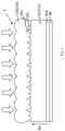
- FIG. 1 is a schematic structure of a micro-channel device with micro-channels at the top according to one embodiment of the present disclosure.
- FIG. 2 is an A-A section according to the schematic structure of the micro-channel device in FIG. 1 .
- FIG. 3 is a schematic structure of a micro-channel device with micro-channels at the bottom according to one embodiment of the present disclosure.
- FIG. 4 is a schematic structure of a micro-channel device with micro-channels at the top according to one embodiment of the present disclosure.
- FIG. 5 is a schematic structure of a micro-channel device with micro-channels at the bottom according to one embodiment of the present disclosure.
- FIG. 6 is a schematic structure of a micro-channel device with micro-channels at the top according to one embodiment of the present disclosure.
- FIG. 7 is a schematic structure of a micro-channel device with micro-channels at the bottom according to one embodiment of the present disclosure.
- FIG. 8 is a schematic structure of a micro-fluidic system according to one embodiment of the present disclosure.
- FIGS. 1 - 8 When referring to the figures, like structures and elements shown throughout are indicated with like reference numerals.
- micro-channel refers to channels having a maximum cross-sectional dimension in the range of approximately 1 nm to approximately 1000 ⁇ m, e.g., approximately 1 nm to approximately 50 nm, approximately 50 nm to approximately 100 nm, approximately 100 nm to approximately 1 ⁇ m, approximately 1 ⁇ m to approximately 10 ⁇ m, approximately 10 ⁇ m to approximately 100 ⁇ m, approximately 100 ⁇ m to approximately 200 ⁇ m, approximately 200 ⁇ m to approximately 400 ⁇ m, approximately 400 ⁇ m to approximately 600 ⁇ m, approximately 600 ⁇ m to approximately 800 ⁇ m, and approximately 800 ⁇ m to approximately 1000 ⁇ m.
- cross-sectional dimension may relate to height, width and in principle also to diameter.
- a micro-channel may have any selected cross-sectional shape, for example, U-shaped, D-shaped, rectangular, triangular, elliptical, oval, circular, semi-circular, square, trapezoidal, pentagonal, hexagonal, etc. cross-sectional geometries.
- the micro-channel has an irregular cross-sectional shape.
- the geometry may be constant or may vary along the length of the micro channel.
- a micro-channel may have any selected arrangement or configuration, including linear, non-linear, merging, branching, looped, twisting, stepped, etc. configurations.
- the micro-channel may have one or more open ends.
- the micro-channel may have one or more closed ends.
- the micro-channel has a closed-wall structure.
- the micro-channel has a partially open-wall structure.
- the micro-channel has a fully open-wall structure, e.g., a micro-groove.
- FIG. 1 is schematic structure of a micro-channel device with micro-channels at the top according to one embodiment of the present disclosure.
- the micro-channel device 1 may include a micro-channel structure 10 and a semiconductor junction 20 .
- the micro-channel structure 10 includes a base layer 101 , a plurality of rails 102 distributed on the base layer 101 at intervals, and a cover layer 103 .
- the cover layer 103 includes a plurality of columns 1030 connected together.
- a surface of the cover layer 103 facing the base layer 101 includes a plurality of ridges and a plurality of valleys, which are alternatively distributed.
- the plurality of ridges is located on the plurality of rails.
- the cover layer 103 and the base layer 101 are configured to form a plurality of micro-channels 104 . That is, the plurality of valleys on the surface of the cover layer 103 facing the base layer 101 and the base layer 101 form the plurality of micro-channels 104 .
- the semiconductor junction 20 includes a P-type semiconductor layer 201 , an intrinsic semiconductor layer 202 and a N-type semiconductor layer 203 stacked in a first direction D 1 , as shown in FIG. 1 .
- FIG. 2 is an A-A section according to the schematic structure of the micro-channel device in FIG. 1 .
- one of the plurality of the micro-channel 104 is between two of the plurality of columns 1030 .
- An orthographic projection of one of the plurality of columns 1030 on the base layer 101 covers an orthographic projection of a corresponding rail 102 on the base layer 101 .
- the orthographic projection of the corresponding rail 102 is located in the middle of the orthographic projection of one of the plurality of columns 1030 .
- each of plurality of rails 102 may have any appropriate cross-sectional shape, for example, rectangular, triangular, elliptical, oval, circular, semi-circular, square, trapezoidal, pentagonal, hexagonal, etc. cross-sectional geometries.
- each of plurality of rails 102 has an irregular cross-sectional shape. The geometry may be constant or may vary along the length of the micro channel.
- each of the plurality of rails 102 may have any selected arrangement or configuration, including linear, non-linear, merging, branching, looped, twisting, stepped, etc. configurations.
- each of the plurality of rails 102 has a linear shape, and extends along a second direction D 2 .
- a corresponding column 1030 and a corresponding micro-channel of the plurality of micro-channels 104 have the same extension directions as the second direction D 2 , and are parallel to each other. That is, the plurality of rails 102 and the plurality of micro-channels 104 are alternatively distributed in parallel with each other on the base layer 101 .
- At least one of the plurality of rails 102 has a S-shape.
- the corresponding column 1030 and the corresponding micro-channel of the plurality of micro-channels 104 have the same shapes as the S-shape. That is, the corresponding column 1030 and the corresponding micro-channel of the plurality of micro-channels 104 follow the same shape or contour of the rail 102 .
- the first direction D 1 is substantially perpendicular to a base substrate 30 . That is, the P-type semiconductor layer 201 , the intrinsic semiconductor layer 202 and the N-type semiconductor layer 203 of the semiconductor junction 20 are formed sequentially on the base substrate 30 .
- the cover layer 103 comprising the plurality of columns 1030 is made of a transparent conductive material.
- the transparent conductive material may include one or more of elements in a group of indium (In), aluminum (Al), gold (Au), silver (Ag) or, indium oxide (In 2 O 3 ), tin oxide (SnO 2 ), zinc oxide (ZnO), cadmium oxide (CdO), indium cadmium oxide (CdIn 2 O 4 ), cadmium tin oxide (Cd 2 SnO 4 ), and zinc tin oxide (Zn 2 SnO 4 ).
- the N-type semiconductor layer 203 is the base layer 101 of the micro-channel structure 10 . That is, the N-type semiconductor layer 203 of the semiconductor junction 20 and the base layer 101 of the micro-channel structure 10 are the same layer.
- the N-type semiconductor layer 203 has a plurality of protruding portions on a surface. The plurality of protruding portions is configured as the plurality of rails 102 .
- the cover layer 103 is directly arranged on the plurality of rails 102 or protruding portions, and in physical contact with the N-type semiconductor layer 203 .
- the plurality of micro-channels 104 are at the top of the micro-channel device.
- FIG. 3 is a schematic structure of a micro-channel device with micro-channels at the bottom according to one embodiment of the present disclosure.
- the base substrate 30 is the base layer 101 of the micro-channel structure 10 . That is, the base substrate 30 and the base layer 101 of the micro-channel structure 10 are the same layer.
- the plurality of rails 102 are formed on the base substrate 30 .
- the semiconductor junction 20 is arranged on a side of the micro-channel structure 10 opposite from the base substrate 30 .
- the plurality of micro-channels 104 are at the bottom of the micro-channel device.
- FIG. 4 is a schematic structure of a micro-channel device with micro-channels at the top according to one embodiment of the present disclosure.
- the cover layer 103 is the same layer as the N-type semiconductor layer 203 ;
- the base layer 101 is the same layer as the intrinsic semiconductor layer 202 ;
- the plurality of rails 102 are made of the same material as the intrinsic semiconductor layer 202 ;
- the plurality of micro-channels 104 are formed between the N-type semiconductor layer 203 and the intrinsic semiconductor layer 202 .
- the plurality of micro-channels 104 are at the top of the micro-channel device.
- the semiconductor junction 20 and the micro-channel structure 10 are integrated together. That is, the N-type semiconductor layer 203 of the semiconductor junction 20 forms the cover layer 103 of the micro-channel structure 10 , and the intrinsic semiconductor layer 202 of the semiconductor junction 20 forms the base layer 101 of the micro-channel structure 10 .
- FIG. 5 is a schematic structure of a micro-channel device with micro-channels at the bottom according to one embodiment of the present disclosure.
- the cover layer 103 is the same layer as the N-type semiconductor layer 203
- the plurality of micro-channels 104 are on a side of the N-type semiconductor layer 203 opposite from the intrinsic semiconductor layer 202 .
- the base layer 101 is the same layer as the base substrate 30 .
- the semiconductor junction 20 is arranged on a side of the micro-channel structure 10 opposite from the base substrate 30 .
- the plurality of micro-channels 104 are at the bottom of the micro-channel device.
- FIG. 6 is a schematic structure of a micro-channel device with micro-channels at the top according to one embodiment of the present disclosure.
- the P-type semiconductor layer 201 , the intrinsic semiconductor layer 202 and the N-type semiconductor layer 203 are stacked in a first direction D 1 , and the first direction D 1 is parallel to the base substrate 30 .
- the cover layer 103 is in parallel with the first direction D 1 ;
- the plurality of rails 102 are on a side surface of the semiconductor junction 20 opposite from the base substrate 30 ;
- the plurality of micro-channels 104 are between the cover layer 103 and the side surface of the semiconductor junction 20 opposite from the base substrate 30 .
- the plurality of micro-channels 104 are at the top of the micro-channel device.
- the plurality of rails 102 are arranged on the side surface of the intrinsic semiconductor layer 202 only.
- the plurality of rails 102 are made of the same material as the intrinsic semiconductor layer 202 .
- FIG. 7 is a schematic structure of a micro-channel device with micro-channels at the bottom according to one embodiment of the present disclosure.
- the P-type semiconductor layer 201 , the intrinsic semiconductor layer 202 and the N-type semiconductor layer 203 are stacked in a first direction D 1 , and the first direction D 1 is parallel to the base substrate 30 .
- the cover layer 103 is in parallel with the first direction D 1 ; and the plurality of rails 102 are on a side surface of the semiconductor junction 20 facing to the base substrate 30 .
- the plurality of micro-channels 104 are on a side of the cover layer 103 opposite from the semiconductor junction 20 , that is, between the base substrate 30 and the cover layer 103 .
- the plurality of micro-channels 104 are at the bottom of the micro-channel device.
- each of the plurality of rails 102 has a distance between approximately 10 nm to approximately 1 ⁇ m from an adjacent rail, for example, approximately 10 nm to approximately 25 nm, approximately 25 nm to approximately 50 nm, approximately 50 nm to approximately 75 nm, approximately 75 nm to approximately 100 nm, approximately 100 nm to approximately 250 nm, approximately 250 nm to approximately 500 nm, approximately 500 nm to approximately 750 nm, or approximately 750 nm to approximately 1 ⁇ m. Adjusting the distance between two adjacent rails can be used to control a width of the micro-channel.
- each of the plurality of rails has a height in a range between approximately 10 nm to approximately 300 nm e.g., approximately 10 nm to approximately 25 nm, approximately 25 nm to approximately 50 nm, approximately 50 nm to approximately 75 nm, approximately 75 nm to approximately 100 nm, or approximately 100 nm to approximately 300 nm. Adjusting the height of each of the plurality of rails may help controlling a height of the micro-channel. The width of the micro-channel and the height of the micro-channel determine the size of a droplet that is able to flow along the micro-channel.
- various appropriate materials may be selected for making the plurality of the rails 102 , the cover layer 103 and the base substrate 30 based on physical and chemical characteristics that are desirable for the function of the micro-channel device.
- Appropriate materials include, but are not limited to, polymeric materials such as silicone polymers (e.g., polydimethylsiloxane and epoxy polymers), polyimides (e.g., commercially available Kapton® (poly(4,4′-oxydiphenylene-pyromellitimide), from DuPont, Wilmington, Del.) and UpilexTM (poly(biphenyl tetracarboxylic dianhydride), from Ube Industries, Ltd., Japan), polycarbonates, polyesters, polyamides, polyethers, polyurethanes, polyfluorocarbons, fluorinated polymers (e.g., polyvinylfluoride, polyvinylidene fluoride, polytetrafluoroethylene, polych
- the present micro-channel device may be used in various appropriate sensors, e.g., a bio-chemical sensor, a gas sensor, a deoxyribonucleic acid (DNA) sensor, a ribonucleic acid (RNA) sensor, a peptide or protein sensor, an antibody sensor, an antigen sensor, a tissue factor sensor, a vector and virus vector sensor, a lipid and fatty acid sensor, a steroid sensor, a neurotransmitter sensor, an inorganic ion and electrochemical sensor, a pH sensor, a free radical sensor, a carbohydrate sensor, a neural sensor, a chemical sensor, a small molecule sensor, an exon sensor, a metabolite sensor, an intermediates sensor, chromosome sensor, and a cell sensor.
- sensors e.g., a bio-chemical sensor, a gas sensor, a deoxyribonucleic acid (DNA) sensor, a ribonucleic acid (RNA) sensor, a peptide or protein sensor,
- the micro-channel device maybe applied in a lab-on-chip device.
- the micro-channel device maybe applied in a gene sequencing apparatus.
- the term “micro-fluidic chip” refers to a small device capable of separating molecules using small volumes and/or flow rates.
- the term “lab-on-chip” refers to an integrated chip on which various scientific operations such as reaction, separation, purification, and detection of sample solution are conducted simultaneously. It is possible to perform ultrahigh-sensitivity analysis, ultra-trace-amount analysis, or ultra-flexible simultaneous multi-item analysis by using a lab-on-chip.
- An example of the lab-on-chip is a chip having a protein-producing unit, a protein-purifying unit, and a protein-detecting unit that are connected to each other via micro-channels.
- the semiconductor junction and the micro-channels are integrated by sharing various specific layers. No bonding process is need, thereby enhancing the alignment between the semiconductor junction and the micro-channels and simplifying the processes.
- the semiconductor junction may be connected to an anode and a cathode respectively to form a PIN diode as a sensor. As such, when the fluidic sample is flowing and passing through the micro-channels, the PIN diode can be used to detect the fluidic sample to get a position signal and/or a composition signal of the fluidic sample.
- the present disclosure provides a micro-fluidic system.
- the micro-fluidic system S includes the micro-channel device 1 described herein according to one embodiment of the present disclosure.
- FIG. 8 is a schematic structure of a micro-fluidic system according to one embodiment of the present disclosure.
- a fluid sample e.g., a gas or a liquid
- the flow control device 2 in some embodiments includes one or a combination of electrophoresis, pressure pumps, and other driving mechanisms.
- the fluid sample flows into a first reservoir 4 which is in turn connected to a micro-channel device 1 according to one embodiment of the present disclosure.
- the first reservoir 4 itself may be a micro-scale channel.
- the fluid sample then flows into the micro-channel, which controls the transport of the fluid sample in the fluidic chip. Under the control of the micro-channel, the fluid sample flows into a second reservoir 5 , a second connection channel 6 , and eventually flows out of the fluidic chip.
- the present disclosure provides a method of manufacturing a micro-channel device described herein according to one embodiment of the present disclosure.
- the method includes forming a micro-channel structure and forming a semiconductor junction.
- the micro-channel structure may include a base layer, a plurality of rails distributed on the base layer at intervals, and a cover layer comprising a plurality of columns.
- the cover layer and the base layer are configured to form a plurality of micro-channels.
- the semiconductor junction may include a P-type semiconductor layer, an intrinsic semiconductor layer and a N-type semiconductor layer stacked in a first direction.
- the forming the micro-channel structure includes patterning the N-type semiconductor layer to form the plurality of rails distributed on a surface of the N-type semiconductor layer.
- patterning methods for forming the plurality of rails include a photolithography process, an electron beam lithography process, a nanoimprint lithography process, an etching process (e.g., dry etching), a hot corrosion process, or any combination thereof.
- the forming the cover layer comprising the plurality of columns is performed by a deposition method.
- deposition methods include sputtering (e.g., magnetron sputtering) and evaporation coating (e.g., a Chemical Vapor Deposition method, a Plasma-Enhanced Chemical Vapor Deposition (PECVD) method, a thermal vapor deposition method, an atomic layer deposition (ALD) method, and an electron beam evaporation method).
- PECVD Plasma-Enhanced Chemical Vapor Deposition
- ALD atomic layer deposition
- the cover layer material is deposited by a sputtering method.
- the plurality of columns is formed by sputtering a transparent conductive material on the plurality of rails.
- micro-channel device 1 micro-channel structure 10 ; base layer 101 ; rail 102 ; cover layer 103 ; column 1030 ; micro-channels 104 ; semiconductor junction 20 ; P-type semiconductor layer 201 ; intrinsic semiconductor layer 202 ; N-type semiconductor layer 203 ; base substrate 30 ; micro-fluidic system S; flow control device 2 ; first connection channel 3 ; first reservoir 4 ; second reservoir 5 ; second connection channel 6 .
Landscapes
- Chemical & Material Sciences (AREA)
- Health & Medical Sciences (AREA)
- Dispersion Chemistry (AREA)
- Analytical Chemistry (AREA)
- General Health & Medical Sciences (AREA)
- Hematology (AREA)
- Clinical Laboratory Science (AREA)
- Chemical Kinetics & Catalysis (AREA)
- Physical Or Chemical Processes And Apparatus (AREA)
Abstract
Description
Claims (11)
Applications Claiming Priority (1)
| Application Number | Priority Date | Filing Date | Title |
|---|---|---|---|
| PCT/CN2019/082873 WO2020210981A1 (en) | 2019-04-16 | 2019-04-16 | Micro-channel device and manufacturing method thereof and micro-fluidic system |
Publications (2)
| Publication Number | Publication Date |
|---|---|
| US20210220824A1 US20210220824A1 (en) | 2021-07-22 |
| US11534755B2 true US11534755B2 (en) | 2022-12-27 |
Family
ID=67725890
Family Applications (1)
| Application Number | Title | Priority Date | Filing Date |
|---|---|---|---|
| US16/755,911 Active 2039-08-03 US11534755B2 (en) | 2019-04-16 | 2019-04-16 | Micro-channel device and manufacturing method thereof and micro-fluidic system |
Country Status (3)
| Country | Link |
|---|---|
| US (1) | US11534755B2 (en) |
| CN (1) | CN110191760B (en) |
| WO (1) | WO2020210981A1 (en) |
Families Citing this family (1)
| Publication number | Priority date | Publication date | Assignee | Title |
|---|---|---|---|---|
| CN113289562B (en) * | 2021-05-28 | 2022-12-02 | 北京京东方技术开发有限公司 | Microfluidic chip, analysis device and control method of microfluidic chip |
Citations (19)
| Publication number | Priority date | Publication date | Assignee | Title |
|---|---|---|---|---|
| WO2001081896A1 (en) | 2000-04-24 | 2001-11-01 | Eagle Research & Development, Llc | An ultra-fast nucleic acid sequencing device and a method for making and using the same |
| US20020018499A1 (en) | 2000-04-06 | 2002-02-14 | Toshiaki Kuniyasu | Semiconductor laser element and semiconductor laser |
| US6433356B1 (en) | 1996-10-29 | 2002-08-13 | Yeda Research And Development Co. Ltd. | Hybrid organic-inorganic semiconductor structures and sensors based thereon |
| US20050014175A1 (en) | 1999-06-28 | 2005-01-20 | California Institute Of Technology | Methods and apparatuses for analyzing polynucleotide sequences |
| KR20050106408A (en) * | 2003-01-31 | 2005-11-09 | 휴렛-팩커드 디벨롭먼트 컴퍼니, 엘 피 | Microfluidic device with thin-film electronic devices |
| US20070151942A1 (en) | 2005-12-29 | 2007-07-05 | Intel Corporation | Apparatus to send biological fluids through a printed wire board |
| CN101013083A (en) | 2007-02-01 | 2007-08-08 | 大连理工大学 | Optical fibre embedded low-voltage actuated capillary tube electrophoresis chip |
| CN101468786A (en) | 2007-12-26 | 2009-07-01 | 中国科学院半导体研究所 | Manufacturing method of silicon carbide microchannel for microelectron mechanical system |
| CN101592627A (en) * | 2009-03-19 | 2009-12-02 | 苏州纳米技术与纳米仿生研究所 | Integrated method for fabricating multi-channel high-sensitivity biosensors |
| CN101765766A (en) | 2007-06-07 | 2010-06-30 | 传感器创新公司 | Semiconductor Electrochemical Sensors |
| CN102150037A (en) | 2008-07-11 | 2011-08-10 | 康奈尔大学 | Nano-fluidic channel of integrated charge sensor and method based on nano-fluidic channel |
| CN102203282A (en) | 2008-06-25 | 2011-09-28 | 生命技术公司 | Methods and apparatus for measuring analytes using large scale fet arrays |
| CN102509728A (en) | 2011-11-01 | 2012-06-20 | 北京大学 | Design and preparation method of non-refrigeration infrared detector |
| CN203445122U (en) | 2013-09-06 | 2014-02-19 | 北京京东方光电科技有限公司 | X-ray detection device array substrate |
| AU2014348306A1 (en) | 2013-11-17 | 2016-06-16 | Quantum-Si Incorporated | Active-source-pixel, integrated device for rapid analysis of biological and chemical specimens |
| US20160244714A1 (en) * | 2013-10-18 | 2016-08-25 | The General Hosptial Corporation | Microfluidic sorting using high gradient magnetic fields |
| CN106197773A (en) | 2016-07-07 | 2016-12-07 | 燕山大学 | A kind of flexible fingertip pressure sensor and preparation method thereof |
| CN109060922A (en) | 2018-08-03 | 2018-12-21 | 京东方科技集团股份有限公司 | A kind of thin film transistor (TFT) and preparation method thereof, sensor |
| US20190056329A1 (en) * | 2017-08-17 | 2019-02-21 | Abbott Point Of Care Inc. | Devices, systems, and methods for performing optical assays |
Family Cites Families (11)
| Publication number | Priority date | Publication date | Assignee | Title |
|---|---|---|---|---|
| ATE403145T1 (en) * | 2000-01-31 | 2008-08-15 | Univ Texas | PORTABLE DEVICE HAVING A SENSOR ARRAY ARRANGEMENT |
| US20050089924A1 (en) * | 2000-08-14 | 2005-04-28 | Chih-Ming Ho | Biosensors and methods for their use |
| JP2005538287A (en) * | 2002-08-15 | 2005-12-15 | エムイーエムエスフロー・アンパルトセルスカブ | Micro liquid processing apparatus and method of using the same |
| FR2883860B1 (en) * | 2005-03-29 | 2007-06-08 | Commissariat Energie Atomique | METHOD FOR MANUFACTURING ENTERRES MICRO-CHANNELS AND MICRO-DEVICE COMPRISING SUCH MICRO-CHANNELS |
| JP2011030522A (en) * | 2009-08-04 | 2011-02-17 | Aida Engineering Ltd | Microfluid device |
| TWI473223B (en) * | 2009-08-19 | 2015-02-11 | 精材科技股份有限公司 | Chip package and method of manufacturing same |
| CN104956487A (en) * | 2012-08-20 | 2015-09-30 | 贺利氏特种光源美国有限责任公司 | Micro-channel-cooled high heat load light emitting device |
| CA2867451C (en) * | 2013-10-28 | 2021-06-29 | Vapor Technologies, Inc. | Low pressure arc plasma immersion coating vapor deposition and ion treatment |
| CN107971049B (en) * | 2017-09-29 | 2020-07-31 | 京东方科技集团股份有限公司 | Micro-fluidic chip and driving method thereof, micro-fluidic device and biosensor |
| CN108816299B (en) * | 2018-04-20 | 2020-03-27 | 京东方科技集团股份有限公司 | Microfluidic substrate, driving method thereof and micro total analysis system |
| CN109603941B (en) * | 2019-01-11 | 2021-08-03 | 京东方科技集团股份有限公司 | Microfluidic chip system and microfluidic chip |
-
2019
- 2019-04-16 CN CN201980000501.0A patent/CN110191760B/en active Active
- 2019-04-16 WO PCT/CN2019/082873 patent/WO2020210981A1/en not_active Ceased
- 2019-04-16 US US16/755,911 patent/US11534755B2/en active Active
Patent Citations (19)
| Publication number | Priority date | Publication date | Assignee | Title |
|---|---|---|---|---|
| US6433356B1 (en) | 1996-10-29 | 2002-08-13 | Yeda Research And Development Co. Ltd. | Hybrid organic-inorganic semiconductor structures and sensors based thereon |
| US20050014175A1 (en) | 1999-06-28 | 2005-01-20 | California Institute Of Technology | Methods and apparatuses for analyzing polynucleotide sequences |
| US20020018499A1 (en) | 2000-04-06 | 2002-02-14 | Toshiaki Kuniyasu | Semiconductor laser element and semiconductor laser |
| WO2001081896A1 (en) | 2000-04-24 | 2001-11-01 | Eagle Research & Development, Llc | An ultra-fast nucleic acid sequencing device and a method for making and using the same |
| KR20050106408A (en) * | 2003-01-31 | 2005-11-09 | 휴렛-팩커드 디벨롭먼트 컴퍼니, 엘 피 | Microfluidic device with thin-film electronic devices |
| US20070151942A1 (en) | 2005-12-29 | 2007-07-05 | Intel Corporation | Apparatus to send biological fluids through a printed wire board |
| CN101013083A (en) | 2007-02-01 | 2007-08-08 | 大连理工大学 | Optical fibre embedded low-voltage actuated capillary tube electrophoresis chip |
| CN101765766A (en) | 2007-06-07 | 2010-06-30 | 传感器创新公司 | Semiconductor Electrochemical Sensors |
| CN101468786A (en) | 2007-12-26 | 2009-07-01 | 中国科学院半导体研究所 | Manufacturing method of silicon carbide microchannel for microelectron mechanical system |
| CN102203282A (en) | 2008-06-25 | 2011-09-28 | 生命技术公司 | Methods and apparatus for measuring analytes using large scale fet arrays |
| CN102150037A (en) | 2008-07-11 | 2011-08-10 | 康奈尔大学 | Nano-fluidic channel of integrated charge sensor and method based on nano-fluidic channel |
| CN101592627A (en) * | 2009-03-19 | 2009-12-02 | 苏州纳米技术与纳米仿生研究所 | Integrated method for fabricating multi-channel high-sensitivity biosensors |
| CN102509728A (en) | 2011-11-01 | 2012-06-20 | 北京大学 | Design and preparation method of non-refrigeration infrared detector |
| CN203445122U (en) | 2013-09-06 | 2014-02-19 | 北京京东方光电科技有限公司 | X-ray detection device array substrate |
| US20160244714A1 (en) * | 2013-10-18 | 2016-08-25 | The General Hosptial Corporation | Microfluidic sorting using high gradient magnetic fields |
| AU2014348306A1 (en) | 2013-11-17 | 2016-06-16 | Quantum-Si Incorporated | Active-source-pixel, integrated device for rapid analysis of biological and chemical specimens |
| CN106197773A (en) | 2016-07-07 | 2016-12-07 | 燕山大学 | A kind of flexible fingertip pressure sensor and preparation method thereof |
| US20190056329A1 (en) * | 2017-08-17 | 2019-02-21 | Abbott Point Of Care Inc. | Devices, systems, and methods for performing optical assays |
| CN109060922A (en) | 2018-08-03 | 2018-12-21 | 京东方科技集团股份有限公司 | A kind of thin film transistor (TFT) and preparation method thereof, sensor |
Non-Patent Citations (6)
| Title |
|---|
| Glick et al. (Fabrication of Double-Sided Microfluidixc Structures via 3D Printed Transfer Molding, Solid-State Sensors, Actuators and Microsystems Workshop, 2016, pp. 153-156) (Year: 2016). * |
| International Search Report dated Jan. 19, 2020, issued in counterpart application No. PCT/CN2019/082873. (10 pages). |
| Kistrup et al. (Ultrasonic welding for fast bonding of self-aligned structures in lab-on-a-chip systems, Lab on a Chip, 2015, 15, pp. 1998-2001,) (Year: 2015). * |
| Lamberti et al. (A Combined Electrochemical-Microfluidic Strategy for the Microscale-Sized Selective Modification of Transparent Conductive Oxides, Advanced Materials Interfaces, 2018, 10 pages (Year: 2018). * |
| Office Action dated Nov. 27, 2020, issued in counterpart CN Application No. 201980000501.0, with English translation (23 pages). |
| Su et al. (CN 101592627, examiner provided machine translation) (Year: 2009). * |
Also Published As
| Publication number | Publication date |
|---|---|
| CN110191760B (en) | 2022-09-27 |
| CN110191760A (en) | 2019-08-30 |
| WO2020210981A1 (en) | 2020-10-22 |
| US20210220824A1 (en) | 2021-07-22 |
Similar Documents
| Publication | Publication Date | Title |
|---|---|---|
| US8388908B2 (en) | Fluidic devices with diaphragm valves | |
| CN109060922B (en) | Thin film transistor, preparation method thereof and sensor | |
| CN101498630B (en) | Sample pretreatment integrated chip | |
| Fan et al. | Droplet-on-a-wristband: Chip-to-chip digital microfluidic interfaces between replaceable and flexible electrowetting modules | |
| JP2004093558A (en) | Analysis chip, analysis chip unit, analysis device, and method of manufacturing analysis chip | |
| CN103386332A (en) | Method of transporting liquid drops by micro-fluidic chip | |
| US20130000764A1 (en) | Multi-layer micro/nanofluid devices with bio-nanovalves | |
| CN112368234A (en) | Micro-nano channel structure, sensor, preparation method of sensor and micro-fluid device | |
| CN1644250A (en) | Sorting particles in parallel | |
| EP1531002A2 (en) | Device and method to electrostatically seal microfluidic devices | |
| CN113145183B (en) | Biological chip and its making method | |
| US11534755B2 (en) | Micro-channel device and manufacturing method thereof and micro-fluidic system | |
| CN101290314A (en) | Microfluidic chip for cell fixation and solution dilution | |
| US20180045667A1 (en) | Sensing apparatus | |
| US8486352B2 (en) | Micro-valve structure including polymer actuator and lab-on-a-chip module | |
| JP5103614B2 (en) | Trace liquid sorting device | |
| US11219899B2 (en) | Micro-channel structure, sensor, micro-fluidic device, lab-on-chip device, and method of fabricating micro-channel structure | |
| KR101454206B1 (en) | Component, Structure and Method for Preventing non-Specific Binding of Polymer Sample, Bio-chip, Bio-chip board, Sample tube, Flow tube and Sample board using the Same | |
| CN111215159B (en) | Microfluidic chip and method for fusing samples based on the chip | |
| CN108195805B (en) | Microfluid sensing element and manufacturing method thereof | |
| CN110523447B (en) | Microfluidic chip for multi-angle mechanical measurement of cells and manufacturing method thereof | |
| Maltezos | Microfluidic Devices for Accessible Medical Diagnostics | |
| CN114534811A (en) | Microfluidic device and manufacturing method thereof | |
| Krishnamoorthy et al. | ON-CHIP ELECTROKINETIC SAMPLE FOCUS-ING FOR MICROARRAY-BASED BIOMOLECULAR INTERACTION ASSAYS | |
| Zhu et al. | Microfluidic single-cell culture chip for individual trapping, cultivation, and selective release of yeast cells |
Legal Events
| Date | Code | Title | Description |
|---|---|---|---|
| AS | Assignment |
Owner name: BOE TECHNOLOGY GROUP CO., LTD., CHINA Free format text: ASSIGNMENT OF ASSIGNORS INTEREST;ASSIGNORS:NING, CE;MA, XIAOCHEN;HU, HEHE;AND OTHERS;REEL/FRAME:052387/0172 Effective date: 20200408 |
|
| FEPP | Fee payment procedure |
Free format text: ENTITY STATUS SET TO UNDISCOUNTED (ORIGINAL EVENT CODE: BIG.); ENTITY STATUS OF PATENT OWNER: LARGE ENTITY |
|
| STPP | Information on status: patent application and granting procedure in general |
Free format text: APPLICATION DISPATCHED FROM PREEXAM, NOT YET DOCKETED |
|
| STPP | Information on status: patent application and granting procedure in general |
Free format text: DOCKETED NEW CASE - READY FOR EXAMINATION |
|
| STPP | Information on status: patent application and granting procedure in general |
Free format text: NON FINAL ACTION MAILED |
|
| STPP | Information on status: patent application and granting procedure in general |
Free format text: RESPONSE TO NON-FINAL OFFICE ACTION ENTERED AND FORWARDED TO EXAMINER |
|
| STPP | Information on status: patent application and granting procedure in general |
Free format text: FINAL REJECTION MAILED |
|
| STPP | Information on status: patent application and granting procedure in general |
Free format text: RESPONSE AFTER FINAL ACTION FORWARDED TO EXAMINER |
|
| STPP | Information on status: patent application and granting procedure in general |
Free format text: ADVISORY ACTION MAILED |
|
| STPP | Information on status: patent application and granting procedure in general |
Free format text: DOCKETED NEW CASE - READY FOR EXAMINATION |
|
| STPP | Information on status: patent application and granting procedure in general |
Free format text: NOTICE OF ALLOWANCE MAILED -- APPLICATION RECEIVED IN OFFICE OF PUBLICATIONS |
|
| STPP | Information on status: patent application and granting procedure in general |
Free format text: AWAITING TC RESP., ISSUE FEE NOT PAID |
|
| STPP | Information on status: patent application and granting procedure in general |
Free format text: NOTICE OF ALLOWANCE MAILED -- APPLICATION RECEIVED IN OFFICE OF PUBLICATIONS |
|
| STPP | Information on status: patent application and granting procedure in general |
Free format text: PUBLICATIONS -- ISSUE FEE PAYMENT VERIFIED |
|
| STCF | Information on status: patent grant |
Free format text: PATENTED CASE |