US11522067B2 - High electron mobility transistor (HEMT) device and method of forming same - Google Patents

High electron mobility transistor (HEMT) device and method of forming same Download PDF

Info

Publication number
US11522067B2
US11522067B2 US17/225,482 US202117225482A US11522067B2 US 11522067 B2 US11522067 B2 US 11522067B2 US 202117225482 A US202117225482 A US 202117225482A US 11522067 B2 US11522067 B2 US 11522067B2
Authority
US
United States
Prior art keywords
layer
iii
compound
compound layer
algan
Prior art date
Legal status (The legal status is an assumption and is not a legal conclusion. Google has not performed a legal analysis and makes no representation as to the accuracy of the status listed.)
Active
Application number
US17/225,482
Other versions
US20210226040A1 (en
Inventor
Chia-Ling Yeh
Ching Yu Chen
Current Assignee (The listed assignees may be inaccurate. Google has not performed a legal analysis and makes no representation or warranty as to the accuracy of the list.)
Taiwan Semiconductor Manufacturing Co TSMC Ltd
Original Assignee
Taiwan Semiconductor Manufacturing Co TSMC Ltd
Priority date (The priority date is an assumption and is not a legal conclusion. Google has not performed a legal analysis and makes no representation as to the accuracy of the date listed.)
Filing date
Publication date
Application filed by Taiwan Semiconductor Manufacturing Co TSMC Ltd filed Critical Taiwan Semiconductor Manufacturing Co TSMC Ltd
Priority to US17/225,482 priority Critical patent/US11522067B2/en
Publication of US20210226040A1 publication Critical patent/US20210226040A1/en
Application granted granted Critical
Publication of US11522067B2 publication Critical patent/US11522067B2/en
Active legal-status Critical Current
Anticipated expiration legal-status Critical

Links

Images

Classifications

    • HELECTRICITY
    • H01ELECTRIC ELEMENTS
    • H01LSEMICONDUCTOR DEVICES NOT COVERED BY CLASS H10
    • H01L29/00Semiconductor devices adapted for rectifying, amplifying, oscillating or switching, or capacitors or resistors with at least one potential-jump barrier or surface barrier, e.g. PN junction depletion layer or carrier concentration layer; Details of semiconductor bodies or of electrodes thereof  ; Multistep manufacturing processes therefor
    • H01L29/66Types of semiconductor device ; Multistep manufacturing processes therefor
    • H01L29/68Types of semiconductor device ; Multistep manufacturing processes therefor controllable by only the electric current supplied, or only the electric potential applied, to an electrode which does not carry the current to be rectified, amplified or switched
    • H01L29/76Unipolar devices, e.g. field effect transistors
    • H01L29/772Field effect transistors
    • H01L29/778Field effect transistors with two-dimensional charge carrier gas channel, e.g. HEMT ; with two-dimensional charge-carrier layer formed at a heterojunction interface
    • H01L29/7786Field effect transistors with two-dimensional charge carrier gas channel, e.g. HEMT ; with two-dimensional charge-carrier layer formed at a heterojunction interface with direct single heterostructure, i.e. with wide bandgap layer formed on top of active layer, e.g. direct single heterostructure MIS-like HEMT
    • HELECTRICITY
    • H01ELECTRIC ELEMENTS
    • H01LSEMICONDUCTOR DEVICES NOT COVERED BY CLASS H10
    • H01L29/00Semiconductor devices adapted for rectifying, amplifying, oscillating or switching, or capacitors or resistors with at least one potential-jump barrier or surface barrier, e.g. PN junction depletion layer or carrier concentration layer; Details of semiconductor bodies or of electrodes thereof  ; Multistep manufacturing processes therefor
    • H01L29/66Types of semiconductor device ; Multistep manufacturing processes therefor
    • H01L29/68Types of semiconductor device ; Multistep manufacturing processes therefor controllable by only the electric current supplied, or only the electric potential applied, to an electrode which does not carry the current to be rectified, amplified or switched
    • H01L29/76Unipolar devices, e.g. field effect transistors
    • H01L29/772Field effect transistors
    • H01L29/778Field effect transistors with two-dimensional charge carrier gas channel, e.g. HEMT ; with two-dimensional charge-carrier layer formed at a heterojunction interface
    • H01L29/7782Field effect transistors with two-dimensional charge carrier gas channel, e.g. HEMT ; with two-dimensional charge-carrier layer formed at a heterojunction interface with confinement of carriers by at least two heterojunctions, e.g. DHHEMT, quantum well HEMT, DHMODFET
    • H01L29/7783Field effect transistors with two-dimensional charge carrier gas channel, e.g. HEMT ; with two-dimensional charge-carrier layer formed at a heterojunction interface with confinement of carriers by at least two heterojunctions, e.g. DHHEMT, quantum well HEMT, DHMODFET using III-V semiconductor material
    • HELECTRICITY
    • H01ELECTRIC ELEMENTS
    • H01LSEMICONDUCTOR DEVICES NOT COVERED BY CLASS H10
    • H01L21/00Processes or apparatus adapted for the manufacture or treatment of semiconductor or solid state devices or of parts thereof
    • H01L21/02Manufacture or treatment of semiconductor devices or of parts thereof
    • H01L21/02104Forming layers
    • H01L21/02107Forming insulating materials on a substrate
    • H01L21/02109Forming insulating materials on a substrate characterised by the type of layer, e.g. type of material, porous/non-porous, pre-cursors, mixtures or laminates
    • H01L21/02205Forming insulating materials on a substrate characterised by the type of layer, e.g. type of material, porous/non-porous, pre-cursors, mixtures or laminates the layer being characterised by the precursor material for deposition
    • HELECTRICITY
    • H01ELECTRIC ELEMENTS
    • H01LSEMICONDUCTOR DEVICES NOT COVERED BY CLASS H10
    • H01L21/00Processes or apparatus adapted for the manufacture or treatment of semiconductor or solid state devices or of parts thereof
    • H01L21/02Manufacture or treatment of semiconductor devices or of parts thereof
    • H01L21/02104Forming layers
    • H01L21/02107Forming insulating materials on a substrate
    • H01L21/02225Forming insulating materials on a substrate characterised by the process for the formation of the insulating layer
    • H01L21/0226Forming insulating materials on a substrate characterised by the process for the formation of the insulating layer formation by a deposition process
    • H01L21/02293Forming insulating materials on a substrate characterised by the process for the formation of the insulating layer formation by a deposition process formation of epitaxial layers by a deposition process
    • HELECTRICITY
    • H01ELECTRIC ELEMENTS
    • H01LSEMICONDUCTOR DEVICES NOT COVERED BY CLASS H10
    • H01L21/00Processes or apparatus adapted for the manufacture or treatment of semiconductor or solid state devices or of parts thereof
    • H01L21/02Manufacture or treatment of semiconductor devices or of parts thereof
    • H01L21/02104Forming layers
    • H01L21/02365Forming inorganic semiconducting materials on a substrate
    • H01L21/02436Intermediate layers between substrates and deposited layers
    • H01L21/02439Materials
    • H01L21/02455Group 13/15 materials
    • H01L21/02458Nitrides
    • HELECTRICITY
    • H01ELECTRIC ELEMENTS
    • H01LSEMICONDUCTOR DEVICES NOT COVERED BY CLASS H10
    • H01L21/00Processes or apparatus adapted for the manufacture or treatment of semiconductor or solid state devices or of parts thereof
    • H01L21/02Manufacture or treatment of semiconductor devices or of parts thereof
    • H01L21/02104Forming layers
    • H01L21/02365Forming inorganic semiconducting materials on a substrate
    • H01L21/02436Intermediate layers between substrates and deposited layers
    • H01L21/02494Structure
    • H01L21/02496Layer structure
    • H01L21/02505Layer structure consisting of more than two layers
    • HELECTRICITY
    • H01ELECTRIC ELEMENTS
    • H01LSEMICONDUCTOR DEVICES NOT COVERED BY CLASS H10
    • H01L21/00Processes or apparatus adapted for the manufacture or treatment of semiconductor or solid state devices or of parts thereof
    • H01L21/02Manufacture or treatment of semiconductor devices or of parts thereof
    • H01L21/02104Forming layers
    • H01L21/02365Forming inorganic semiconducting materials on a substrate
    • H01L21/02518Deposited layers
    • H01L21/02521Materials
    • H01L21/02538Group 13/15 materials
    • H01L21/0254Nitrides
    • HELECTRICITY
    • H01ELECTRIC ELEMENTS
    • H01LSEMICONDUCTOR DEVICES NOT COVERED BY CLASS H10
    • H01L21/00Processes or apparatus adapted for the manufacture or treatment of semiconductor or solid state devices or of parts thereof
    • H01L21/02Manufacture or treatment of semiconductor devices or of parts thereof
    • H01L21/02104Forming layers
    • H01L21/02365Forming inorganic semiconducting materials on a substrate
    • H01L21/02518Deposited layers
    • H01L21/0257Doping during depositing
    • H01L21/02573Conductivity type
    • H01L21/02579P-type
    • HELECTRICITY
    • H01ELECTRIC ELEMENTS
    • H01LSEMICONDUCTOR DEVICES NOT COVERED BY CLASS H10
    • H01L21/00Processes or apparatus adapted for the manufacture or treatment of semiconductor or solid state devices or of parts thereof
    • H01L21/02Manufacture or treatment of semiconductor devices or of parts thereof
    • H01L21/02104Forming layers
    • H01L21/02365Forming inorganic semiconducting materials on a substrate
    • H01L21/02518Deposited layers
    • H01L21/0257Doping during depositing
    • H01L21/02573Conductivity type
    • H01L21/02581Transition metal or rare earth elements
    • HELECTRICITY
    • H01ELECTRIC ELEMENTS
    • H01LSEMICONDUCTOR DEVICES NOT COVERED BY CLASS H10
    • H01L21/00Processes or apparatus adapted for the manufacture or treatment of semiconductor or solid state devices or of parts thereof
    • H01L21/02Manufacture or treatment of semiconductor devices or of parts thereof
    • H01L21/02104Forming layers
    • H01L21/02365Forming inorganic semiconducting materials on a substrate
    • H01L21/02612Formation types
    • H01L21/02617Deposition types
    • H01L21/0262Reduction or decomposition of gaseous compounds, e.g. CVD
    • HELECTRICITY
    • H01ELECTRIC ELEMENTS
    • H01LSEMICONDUCTOR DEVICES NOT COVERED BY CLASS H10
    • H01L21/00Processes or apparatus adapted for the manufacture or treatment of semiconductor or solid state devices or of parts thereof
    • H01L21/67Apparatus specially adapted for handling semiconductor or electric solid state devices during manufacture or treatment thereof; Apparatus specially adapted for handling wafers during manufacture or treatment of semiconductor or electric solid state devices or components ; Apparatus not specifically provided for elsewhere
    • H01L21/67005Apparatus not specifically provided for elsewhere
    • H01L21/67011Apparatus for manufacture or treatment
    • H01L21/67017Apparatus for fluid treatment
    • HELECTRICITY
    • H01ELECTRIC ELEMENTS
    • H01LSEMICONDUCTOR DEVICES NOT COVERED BY CLASS H10
    • H01L21/00Processes or apparatus adapted for the manufacture or treatment of semiconductor or solid state devices or of parts thereof
    • H01L21/67Apparatus specially adapted for handling semiconductor or electric solid state devices during manufacture or treatment thereof; Apparatus specially adapted for handling wafers during manufacture or treatment of semiconductor or electric solid state devices or components ; Apparatus not specifically provided for elsewhere
    • H01L21/67005Apparatus not specifically provided for elsewhere
    • H01L21/67011Apparatus for manufacture or treatment
    • H01L21/67098Apparatus for thermal treatment
    • HELECTRICITY
    • H01ELECTRIC ELEMENTS
    • H01LSEMICONDUCTOR DEVICES NOT COVERED BY CLASS H10
    • H01L21/00Processes or apparatus adapted for the manufacture or treatment of semiconductor or solid state devices or of parts thereof
    • H01L21/67Apparatus specially adapted for handling semiconductor or electric solid state devices during manufacture or treatment thereof; Apparatus specially adapted for handling wafers during manufacture or treatment of semiconductor or electric solid state devices or components ; Apparatus not specifically provided for elsewhere
    • H01L21/67005Apparatus not specifically provided for elsewhere
    • H01L21/67242Apparatus for monitoring, sorting or marking
    • H01L21/67248Temperature monitoring
    • HELECTRICITY
    • H01ELECTRIC ELEMENTS
    • H01LSEMICONDUCTOR DEVICES NOT COVERED BY CLASS H10
    • H01L21/00Processes or apparatus adapted for the manufacture or treatment of semiconductor or solid state devices or of parts thereof
    • H01L21/70Manufacture or treatment of devices consisting of a plurality of solid state components formed in or on a common substrate or of parts thereof; Manufacture of integrated circuit devices or of parts thereof
    • H01L21/71Manufacture of specific parts of devices defined in group H01L21/70
    • H01L21/768Applying interconnections to be used for carrying current between separate components within a device comprising conductors and dielectrics
    • H01L21/76897Formation of self-aligned vias or contact plugs, i.e. involving a lithographically uncritical step
    • HELECTRICITY
    • H01ELECTRIC ELEMENTS
    • H01LSEMICONDUCTOR DEVICES NOT COVERED BY CLASS H10
    • H01L23/00Details of semiconductor or other solid state devices
    • H01L23/28Encapsulations, e.g. encapsulating layers, coatings, e.g. for protection
    • H01L23/31Encapsulations, e.g. encapsulating layers, coatings, e.g. for protection characterised by the arrangement or shape
    • H01L23/3157Partial encapsulation or coating
    • H01L23/3171Partial encapsulation or coating the coating being directly applied to the semiconductor body, e.g. passivation layer
    • HELECTRICITY
    • H01ELECTRIC ELEMENTS
    • H01LSEMICONDUCTOR DEVICES NOT COVERED BY CLASS H10
    • H01L23/00Details of semiconductor or other solid state devices
    • H01L23/28Encapsulations, e.g. encapsulating layers, coatings, e.g. for protection
    • H01L23/31Encapsulations, e.g. encapsulating layers, coatings, e.g. for protection characterised by the arrangement or shape
    • H01L23/3157Partial encapsulation or coating
    • H01L23/3192Multilayer coating
    • HELECTRICITY
    • H01ELECTRIC ELEMENTS
    • H01LSEMICONDUCTOR DEVICES NOT COVERED BY CLASS H10
    • H01L29/00Semiconductor devices adapted for rectifying, amplifying, oscillating or switching, or capacitors or resistors with at least one potential-jump barrier or surface barrier, e.g. PN junction depletion layer or carrier concentration layer; Details of semiconductor bodies or of electrodes thereof  ; Multistep manufacturing processes therefor
    • H01L29/02Semiconductor bodies ; Multistep manufacturing processes therefor
    • H01L29/12Semiconductor bodies ; Multistep manufacturing processes therefor characterised by the materials of which they are formed
    • H01L29/20Semiconductor bodies ; Multistep manufacturing processes therefor characterised by the materials of which they are formed including, apart from doping materials or other impurities, only AIIIBV compounds
    • H01L29/2003Nitride compounds
    • HELECTRICITY
    • H01ELECTRIC ELEMENTS
    • H01LSEMICONDUCTOR DEVICES NOT COVERED BY CLASS H10
    • H01L29/00Semiconductor devices adapted for rectifying, amplifying, oscillating or switching, or capacitors or resistors with at least one potential-jump barrier or surface barrier, e.g. PN junction depletion layer or carrier concentration layer; Details of semiconductor bodies or of electrodes thereof  ; Multistep manufacturing processes therefor
    • H01L29/02Semiconductor bodies ; Multistep manufacturing processes therefor
    • H01L29/12Semiconductor bodies ; Multistep manufacturing processes therefor characterised by the materials of which they are formed
    • H01L29/20Semiconductor bodies ; Multistep manufacturing processes therefor characterised by the materials of which they are formed including, apart from doping materials or other impurities, only AIIIBV compounds
    • H01L29/201Semiconductor bodies ; Multistep manufacturing processes therefor characterised by the materials of which they are formed including, apart from doping materials or other impurities, only AIIIBV compounds including two or more compounds, e.g. alloys
    • H01L29/205Semiconductor bodies ; Multistep manufacturing processes therefor characterised by the materials of which they are formed including, apart from doping materials or other impurities, only AIIIBV compounds including two or more compounds, e.g. alloys in different semiconductor regions, e.g. heterojunctions
    • HELECTRICITY
    • H01ELECTRIC ELEMENTS
    • H01LSEMICONDUCTOR DEVICES NOT COVERED BY CLASS H10
    • H01L29/00Semiconductor devices adapted for rectifying, amplifying, oscillating or switching, or capacitors or resistors with at least one potential-jump barrier or surface barrier, e.g. PN junction depletion layer or carrier concentration layer; Details of semiconductor bodies or of electrodes thereof  ; Multistep manufacturing processes therefor
    • H01L29/66Types of semiconductor device ; Multistep manufacturing processes therefor
    • H01L29/66007Multistep manufacturing processes
    • H01L29/66075Multistep manufacturing processes of devices having semiconductor bodies comprising group 14 or group 13/15 materials
    • H01L29/66227Multistep manufacturing processes of devices having semiconductor bodies comprising group 14 or group 13/15 materials the devices being controllable only by the electric current supplied or the electric potential applied, to an electrode which does not carry the current to be rectified, amplified or switched, e.g. three-terminal devices
    • H01L29/66409Unipolar field-effect transistors
    • H01L29/66431Unipolar field-effect transistors with a heterojunction interface channel or gate, e.g. HFET, HIGFET, SISFET, HJFET, HEMT
    • HELECTRICITY
    • H01ELECTRIC ELEMENTS
    • H01LSEMICONDUCTOR DEVICES NOT COVERED BY CLASS H10
    • H01L29/00Semiconductor devices adapted for rectifying, amplifying, oscillating or switching, or capacitors or resistors with at least one potential-jump barrier or surface barrier, e.g. PN junction depletion layer or carrier concentration layer; Details of semiconductor bodies or of electrodes thereof  ; Multistep manufacturing processes therefor
    • H01L29/66Types of semiconductor device ; Multistep manufacturing processes therefor
    • H01L29/66007Multistep manufacturing processes
    • H01L29/66075Multistep manufacturing processes of devices having semiconductor bodies comprising group 14 or group 13/15 materials
    • H01L29/66227Multistep manufacturing processes of devices having semiconductor bodies comprising group 14 or group 13/15 materials the devices being controllable only by the electric current supplied or the electric potential applied, to an electrode which does not carry the current to be rectified, amplified or switched, e.g. three-terminal devices
    • H01L29/66409Unipolar field-effect transistors
    • H01L29/66446Unipolar field-effect transistors with an active layer made of a group 13/15 material, e.g. group 13/15 velocity modulation transistor [VMT], group 13/15 negative resistance FET [NERFET]
    • H01L29/66462Unipolar field-effect transistors with an active layer made of a group 13/15 material, e.g. group 13/15 velocity modulation transistor [VMT], group 13/15 negative resistance FET [NERFET] with a heterojunction interface channel or gate, e.g. HFET, HIGFET, SISFET, HJFET, HEMT
    • HELECTRICITY
    • H01ELECTRIC ELEMENTS
    • H01LSEMICONDUCTOR DEVICES NOT COVERED BY CLASS H10
    • H01L29/00Semiconductor devices adapted for rectifying, amplifying, oscillating or switching, or capacitors or resistors with at least one potential-jump barrier or surface barrier, e.g. PN junction depletion layer or carrier concentration layer; Details of semiconductor bodies or of electrodes thereof  ; Multistep manufacturing processes therefor
    • H01L29/02Semiconductor bodies ; Multistep manufacturing processes therefor
    • H01L29/06Semiconductor bodies ; Multistep manufacturing processes therefor characterised by their shape; characterised by the shapes, relative sizes, or dispositions of the semiconductor regions ; characterised by the concentration or distribution of impurities within semiconductor regions
    • H01L29/10Semiconductor bodies ; Multistep manufacturing processes therefor characterised by their shape; characterised by the shapes, relative sizes, or dispositions of the semiconductor regions ; characterised by the concentration or distribution of impurities within semiconductor regions with semiconductor regions connected to an electrode not carrying current to be rectified, amplified or switched and such electrode being part of a semiconductor device which comprises three or more electrodes
    • H01L29/1066Gate region of field-effect devices with PN junction gate
    • HELECTRICITY
    • H01ELECTRIC ELEMENTS
    • H01LSEMICONDUCTOR DEVICES NOT COVERED BY CLASS H10
    • H01L29/00Semiconductor devices adapted for rectifying, amplifying, oscillating or switching, or capacitors or resistors with at least one potential-jump barrier or surface barrier, e.g. PN junction depletion layer or carrier concentration layer; Details of semiconductor bodies or of electrodes thereof  ; Multistep manufacturing processes therefor
    • H01L29/40Electrodes ; Multistep manufacturing processes therefor
    • H01L29/41Electrodes ; Multistep manufacturing processes therefor characterised by their shape, relative sizes or dispositions
    • H01L29/417Electrodes ; Multistep manufacturing processes therefor characterised by their shape, relative sizes or dispositions carrying the current to be rectified, amplified or switched
    • H01L29/41725Source or drain electrodes for field effect devices
    • H01L29/41766Source or drain electrodes for field effect devices with at least part of the source or drain electrode having contact below the semiconductor surface, e.g. the source or drain electrode formed at least partially in a groove or with inclusions of conductor inside the semiconductor
    • HELECTRICITY
    • H01ELECTRIC ELEMENTS
    • H01LSEMICONDUCTOR DEVICES NOT COVERED BY CLASS H10
    • H01L2924/00Indexing scheme for arrangements or methods for connecting or disconnecting semiconductor or solid-state bodies as covered by H01L24/00
    • H01L2924/10Details of semiconductor or other solid state devices to be connected
    • H01L2924/102Material of the semiconductor or solid state bodies
    • H01L2924/1025Semiconducting materials
    • H01L2924/1026Compound semiconductors
    • H01L2924/1032III-V
    • H01L2924/1033Gallium nitride [GaN]
    • HELECTRICITY
    • H01ELECTRIC ELEMENTS
    • H01LSEMICONDUCTOR DEVICES NOT COVERED BY CLASS H10
    • H01L2924/00Indexing scheme for arrangements or methods for connecting or disconnecting semiconductor or solid-state bodies as covered by H01L24/00
    • H01L2924/10Details of semiconductor or other solid state devices to be connected
    • H01L2924/102Material of the semiconductor or solid state bodies
    • H01L2924/1025Semiconducting materials
    • H01L2924/1026Compound semiconductors
    • H01L2924/1032III-V
    • H01L2924/10344Aluminium gallium nitride [AlGaN]

Definitions

  • Group III-Group V (or III-V) semiconductor compounds are used to form various integrated circuit devices, such as high power field-effect transistors, high frequency transistors, and High Electron Mobility Transistors (HEMTs).
  • a HEMT is a field effect transistor incorporating a 2-Dimensional Electron Gas (2DEG) layer or a Two-Dimensional Hole Gas (2DHG) layer close to the junction between two materials with different band gaps (referred to as a heterojunction).
  • the 2DEG layer instead of a doped region as is generally the case for Metal Oxide Semiconductor Field Effect Transistors (MOSFETs), acts as the channel.
  • MOSFETs Metal Oxide Semiconductor Field Effect Transistors
  • the HEMTs have a number of attractive properties including high electron mobility, the ability to transmit signals at high frequencies, and the like.
  • FIGS. 1 - 5 , 6 A, 6 B, and 7 - 18 illustrate cross-sectional views of various intermediary steps of forming a HEMT device in accordance with some embodiments.
  • FIG. 19 is a flow diagram illustrating a method of forming a HEMT device in accordance with some embodiments.
  • first and second features are formed in direct contact
  • additional features may be formed between the first and second features, such that the first and second features may not be in direct contact
  • present disclosure may repeat reference numerals and/or letters in the various examples. This repetition is for the purpose of simplicity and clarity and does not in itself dictate a relationship between the various embodiments and/or configurations discussed.
  • spatially relative terms such as “beneath,” “below,” “lower,” “above,” “upper” and the like, may be used herein for ease of description to describe one element or feature's relationship to another element(s) or feature(s) as illustrated in the figures.
  • the spatially relative terms are intended to encompass different orientations of the device in use or operation in addition to the orientation depicted in the figures.
  • the apparatus may be otherwise oriented (rotated 90 degrees or at other orientations) and the spatially relative descriptors used herein may likewise be interpreted accordingly.
  • Various embodiments are directed to a semiconductor device, such as a high electron mobility transistor (HEMT) device, and a method of forming the same.
  • the HEMT device includes a multi-barrier layer structure having different polarizations, where a portion of a top high polarization barrier layer is removed over a channel region of the HEMT device, which allows for forming the HEMT device having a high threshold voltage (V th ).
  • V th high threshold voltage
  • the multi-barrier layer structure allows for tuning a carrier (such as, for example, electron or hole) concentration in a channel layer (such as, for example, a two-dimensional electron gas [2DEG] or a two-dimensional hole gas [2DHG]) of the HEMT device and allows for decreasing an on-resistance (R on ) of the HEMT device.
  • a carrier such as, for example, electron or hole
  • a channel layer such as, for example, a two-dimensional electron gas [2DEG] or a two-dimensional hole gas [2DHG]
  • R on on-resistance
  • the top high polarization barrier layer also yields a high band gap that reduces carrier trapping and results in a low dynamical on-resistance (dR on ).
  • the top high polarization barrier layer of the multi-barrier layer structure is formed over an underlying low polarization barrier layer of the multi-barrier layer structure using a low-temperature growth process that reduces a roughness of an interface between the top high polarization barrier layer and the underlying low polarization barrier layer that in turn reduces carrier trapping and results in a low dR on .
  • FIGS. 1 through 18 illustrate cross-sectional views of various intermediary steps of forming a HEMT device 100 in accordance with some embodiments.
  • the HEMT device 100 is formed using a gate-last approach, in which a gate electrode is formed after the formation of source/drain electrodes.
  • the HEMT device 100 may also be formed using a gate-first approach, in which a gate electrode is formed before the formation of source/drain electrodes.
  • the substrate 101 may be a part of an un-singulated wafer.
  • the substrate 101 may comprise, for example, bulk silicon, doped or undoped, or an active layer of a semiconductor-on-insulator (SOI) substrate.
  • SOI substrate comprises a layer of a semiconductor material, such as silicon, formed on an insulator layer.
  • the insulator layer may be, for example, a buried oxide (BOX) layer or a silicon oxide layer.
  • the insulator layer is provided on a substrate, such as a silicon or glass substrate.
  • the substrate 101 may include another elementary semiconductor, such as germanium; a compound semiconductor including silicon carbide, gallium arsenic, gallium phosphide, indium phosphide, indium arsenide, and/or indium antimonide; an alloy semiconductor including SiGe, GaAsP, AlInAs, AlGaAs, GaInAs, GaInP, and/or GaInAsP; or combinations thereof.
  • Other substrates such as multi-layered or gradient substrates, may also be used.
  • a buffer layer 103 is formed over the substrate 101 .
  • the buffer layer 103 acts as the buffer and/or the transition layer for the subsequently formed overlying layers.
  • the buffer layer 103 may comprise a III-V compound, such as aluminum nitride (AlN).
  • the buffer layer 103 may comprise other III-V compounds, such as aluminum arsenide (AlAs), or the like.
  • the buffer layer 103 may be epitaxially grown using metal-organic chemical vapor deposition (MOCVD), molecular beam epitaxy (MBE), liquid phase epitaxy (LPE), vapor phase epitaxy (VPE), metal organic vapor phase epitaxy (MOVPE), selective epitaxial growth (SEG), a combination thereof, or the like.
  • MOCVD metal-organic chemical vapor deposition
  • MBE molecular beam epitaxy
  • LPE liquid phase epitaxy
  • VPE vapor phase epitaxy
  • MOVPE metal organic vapor phase epitaxy
  • SEG selective epitaxial growth
  • a buffer layer 201 is formed over the buffer layer 103 .
  • the buffer layer 201 comprises a III-V compound, such as aluminum gallium nitride (AlGaN), indium aluminum gallium nitride (InAlGaN), or the like.
  • AlGaN aluminum gallium nitride
  • InAlGaN indium aluminum gallium nitride
  • the buffer layer 201 may be epitaxially grown over the buffer layer 103 using similar methods as the buffer layer 103 described above with reference to FIG. 1 , and the description is not repeated herein.
  • the buffer layer 201 has a thickness between about 100 nm and about 5000 nm.
  • the buffer layer 201 may be a graded buffer layer, which means that the relative amounts of the respective aluminum and/or gallium content change with depth in the layer throughout a part or the total thickness of the buffer layer 201 .
  • the relative amounts may change gradually to reduce the lattice parameter with the distance from the substrate 101 .
  • FIG. 2 schematically illustrates three sub-layers 201 A, 201 B, and 201 C of the buffer layer 201 , with the amounts of aluminum and/or gallium in the sub-layers 201 A, 201 B, and 201 C being different from each other.
  • the sub-layer 201 A comprises Al x Ga 1-x N
  • the sub-layer 201 B comprises Al y Ga 1-y N
  • the sub-layer 201 C comprises Al z Ga 1-z N, with x being greater than y, and y being greater than z.
  • a III-V compound layer 301 is formed over the buffer layer 201 .
  • the III-V compound layer 301 comprises gallium nitride (GaN), or the like.
  • the III-V compound layer 301 may be epitaxially grown over the buffer layer 201 using similar methods as the buffer layer 103 described above with reference to FIG. 1 , and the description is not repeated herein.
  • the III-V compound layer 301 may be epitaxially grown by using, for example, MOVPE, during which a gallium-containing precursor and a nitrogen-containing precursor are used.
  • the gallium-containing precursor may include trimethylgallium (TMG), triethylgallium (TEG), other suitable gallium-containing chemicals, a combination thereof, or the like.
  • the nitrogen-containing precursor may include ammonia (NH 3 ), tertiarybutylamine (TBAm), phenyl hydrazine, other suitable nitrogen-containing chemicals, a combination thereof, or the like.
  • the III-V compound layer 301 has a thickness between about 200 nm and about 5000 nm.
  • the III-V compound layer 301 may be doped using suitable dopants.
  • the III-V compound layer 301 may be carbon (C) doped or iron (Fe) doped.
  • the III-V compound layer 301 may be in situ doped while epitaxially growing the III-V compound layer 301 .
  • the epitaxial growing process may further include a carbon-containing precursor or an iron-containing precursor.
  • the carbon-containing precursor may include methane (CH 4 ), ethylene (C 2 H 4 ), acetylene (C 2 H 2 ), propane (C 3 H 8 ), iso-butane (i-C 4 H 10 ), trimethylamine [N(CH 3 ) 3 ], carbon tetrachloride (CCl 4 ), a combination thereof, or the like.
  • the iron-containing precursor may include Bis(cyclopentadienyl)iron [(C 5 H 5 ) 2 Fe], pentacarbonyl iron [(CO) 5 Fe], the like.
  • the III-V compound layer 301 may be doped after the formation of the III-V compound layer 301 is completed.
  • the III-V compound layer 301 may be doped using an implantation method, or the like. In some embodiments, the III-V compound layer 301 is a semi-insulating layer. In some embodiments, the III-V compound layer 301 improves leakage and breakdown performances of the HEMT device 100 .
  • a III-V compound layer 401 is formed over the III-V compound layer 301 .
  • the III-V compound layer 401 comprises a III-V compound, such as gallium nitride (GaN), or the like.
  • the III-V compound layer 401 may be epitaxially grown using similar method as the III-V compound layer 301 described above with reference to FIG. 3 , and the description is not repeated herein.
  • the III-V compound layer 401 has a thickness between about 300 nm and about 3000 nm.
  • the III-V compound layer 401 may be undoped.
  • the III-V compound layer 401 is unintentionally doped, such as lightly doped with n-type (or p-type) dopants due to a precursor used for forming the III-V compound layer 401 , with no dopant that may cause the III-V compound layer 401 to be n-type or p-type intentionally added.
  • a III-V compound layer 501 is formed over the III-V compound layer 401 .
  • the III-V compound layer 501 may also referred to as a barrier layer or a polarization layer.
  • the III-V compound layer 501 has a band gap higher than the band gap of the III-V compound layer 401 .
  • the III-V compound layer 501 generates a quantum well within the III-V compound layer 401 near an interface 503 between the III-V compound layer 501 and III-V compound layer 401 .
  • the quantum well traps carriers, such as electrons or holes, and forms a channel layer 505 (shown as a dashed line in FIG.
  • a thickness of the dashed line of the channel layer illustrates a carrier concentration within the channel layer 505 .
  • the channel layer 505 has high electron mobility partly because the III-V compound layer 401 is undoped or unintentionally doped and the carriers (such as, electrons or holes) can move freely without collision or with substantially reduced collisions with impurities (such as, for example, unintentionally introduced dopants).
  • the III-V compound layer 501 comprises AlGaN, or the like.
  • an aluminum content in the III-V compound layer 501 may be altered relative to a gallium content to alter a polarization strength of the III-V compound layer 501 .
  • the aluminum content x in the III-V compound layer 501 formed of Al x Ga 1-x N may be between about 0.7 and about 0.6.
  • the III-V compound layer 501 may be epitaxially grown over the III-V compound layer 401 using MOCVD, MBE, LPE, VPE, MOVPE, SEG, combinations thereof, or the like.
  • the III-V compound layer 501 may be grown by a MOVPE process using an aluminum-containing precursor, a gallium-containing precursor, and a nitrogen-containing precursor.
  • the aluminum-containing precursor may include trimethylaluminum (TMA), triethylaluminium (TEA), other suitable aluminum-containing chemicals, a combination thereof, or the like.
  • TMA trimethylaluminum
  • TEA triethylaluminium
  • the gallium-containing precursor and the nitrogen-containing precursor may be selected from the same candidate precursors used for forming the III-V compound layers 301 and 401 described above with reference to FIGS. 3 and 4 , respectively, and the description is not repeated herein.
  • the III-V compound layer 501 has a thickness between about 10 nm and about 30 nm.
  • a III-V compound layer 601 is formed over the III-V compound layer 501 .
  • the III-V compound layer 601 may comprise GaN, p-doped aluminum gallium nitride (p-AlGaN), or the like.
  • the III-V compound layer 601 may be formed using similar methods as the III-V compound layers 301 and 401 , described above with reference to FIGS. 3 and 4 , respectively, and the description is not repeated herein.
  • the III-V compound layer 601 may be epitaxially grown by using, for example, MOVPE, during which a gallium-containing precursor and a nitrogen-containing precursor are used.
  • the gallium-containing precursor and the nitrogen-containing precursor may be selected from the same candidate precursors used for forming the III-V compound layers 301 and 401 described above with reference to FIGS. 3 and 4 , respectively, and the description is not repeated herein.
  • the III-V compound layer 601 is p-doped. In some embodiments where the III-V compound layer 601 comprises GaN, the III-V compound layer 601 may be p-doped using magnesium (Mg), zinc (Zn), a combination thereof, or the like. In some embodiments, the III-V compound layer 601 may be in situ doped while epitaxially growing the III-V compound layer 601 . In such embodiments, the MOVPE process may further include a magnesium-containing precursor, a zinc-containing precursor, or a combination thereof.
  • the magnesium-containing precursor may include bis-cyclopentadienyl magnesium (Cp 2 Mg), bismethylcyclopentadienyl magnesium [(MeCp) 2 Mg], bisethylcyclopentadienyl magnesium (ECp 2 Mg), a combination thereof, or the like.
  • the zinc-containing precursor may include diethylzinc (DEZn), or the like.
  • the III-V compound layer 601 may be doped after the formation of the III-V compound layer 601 is completed. In such embodiments, the III-V compound layer 601 may be doped using an implantation method, or the like. In some embodiments, an annealing process may be performed to activate the dopants. In some embodiments, the III-V compound layer 601 has a thickness between about 10 nm and about 500 nm.
  • the III-V compound layer 601 is patterned to remove portions of the III-V compound layer 601 over the III-V compound layer 501 .
  • the III-V compound layer 601 may be patterned using suitable photolithography and etching methods.
  • the patterned III-V compound layer 601 has a width W 1 between about 1 ⁇ m and about 20 ⁇ m.
  • the patterned III-V compound layer 601 depletes carriers in a channel region 603 of the channel layer 505 (illustrated by absence of the dashed line in the channel region 603 of the channel layer 505 ) that is located directly below the patterned III-V compound layer 601 .
  • Portions of the channel layer 505 on either side of the channel region 603 may form access regions 605 , which may also referred to as sourced/drain regions 605 .
  • the channel layer 505 has a non-uniform carrier concentration, with the carriers having a higher concentration in the access regions 605 than in the channel region 603 .
  • a gate electrode is formed over the patterned III-V compound layer 601 that allows for tuning the carrier concentration in the channel region 603 of the channel layer 505 .
  • the patterned III-V compound layer 601 may be a part of a gate structure formed over the channel region 603 of the channel layer 505 .
  • a threshold voltage (V th ) of the HEMT device 100 may be increased.
  • a passivation layer 701 is formed over the III-V compound layers 501 and 601 .
  • the passivation layer 701 may comprise silicon oxide, silicon nitride, silicon oxynitride, a combination thereof, or the like, and may be formed using chemical vapor deposition (CVD), atomic layer deposition (ALD), a combination thereof, or the like.
  • the passivation layer 701 may have a thickness between about 1 ⁇ m and about 10 ⁇ m.
  • the passivation layer 701 is patterned to expose portions of the III-V compound layer 501 not covered by the III-V compound layer 601 . Furthermore, the passivation layer 701 is patterned such that a remaining portion of the passivation layer 701 covers a top surface and sidewall of the III-V compound layer 601 . In some embodiments, the remaining portion of the passivation layer 701 protects the III-V compound layer 601 from subsequent process steps. In some embodiments, the passivation layer 701 is patterned using suitable photolithography and etching methods.
  • a III-V compound layer 901 is formed over the exposed portions of the III-V compound layer 501 on either side of the III-V compound layer 601 .
  • the III-V compound layer 901 has a band gap higher than the band gap of the III-V compound layer 401 .
  • the III-V compound layer 901 may also be referred to as a barrier layer or a polarization layer.
  • the III-V compound layer 901 may comprise AlGaN, or the like.
  • an aluminum content in the III-V compound layer 901 may be altered relative to a gallium content to alter a polarization strength of the III-V compound layer 901 .
  • the III-V compound layer 901 may have a greater aluminum content than the III-V compound layer 501 . In such embodiments, the III-V compound layer 901 has a higher polarization strength than the III-V compound layer 501 .
  • the aluminum content y in the III-V compound layer 901 formed of Al y Ga 1-y N may be between about 0.7 and about 0.6.
  • a ratio of the aluminum content y in the III-V compound layer 901 formed of Al y Ga 1-y N over the aluminum content x in the III-V compound layer 501 formed of Al x Ga 1-x N is between about 1.1 and about 2.5.
  • the carrier concentration in the channel layer 505 is further altered.
  • the carrier concentration in the channel layer 505 is altered such that the carrier concentration in the access regions 605 of the channel layer 505 directly below the III-V compound layer 901 is greater than the carrier concentration in the access regions 605 of the channel layer 505 directly below the passivation layer 701 .
  • an on-resistance (dR on ) of the HEMT device 100 is lowered.
  • the III-V compound layers 501 and 901 form a multi-barrier layer structure over the III-V compound layer 401 .
  • the multi-barrier layer structure comprises two layers (such as the III-V compound layers 501 and 901 ). In other embodiments, the multi-barrier layer structure may comprise more than two layers according to design specifications of the HEMT device 100 .
  • the threshold voltage (V th ) is between about ⁇ 6 V and about +6 V.
  • the III-V compound layer 901 is epitaxially grown over the III-V compound layer 501 using MOCVD, MBE, LPE, VPE, MOVPE, SEG, combinations thereof, or the like. In some embodiments, the III-V compound layer 901 is selectively grown over the exposed portions of the III-V compound layer 501 , such that no portion of the III-V compound layer 901 is formed over the passivation layer 701 . In some embodiments where the III-V compound layer 901 comprises AlGaN, the III-V compound layer 901 may be epitaxially grown using an aluminum-containing precursor, a gallium-containing precursor, and a nitrogen-containing precursor.
  • the aluminum-containing precursor, the gallium-containing precursor and the nitrogen-containing precursor may be selected from the same candidate precursors used for forming the III-V compound layer 501 described above with reference to FIG. 5 , and the description is not repeated herein.
  • the III-V compound layer 901 has a thickness between about 1 nm and about 50 nm.
  • a method of forming the III-V compound layer 901 includes introducing the substrate 101 with the passivation layer 701 and the III-V compound layers 501 and 601 formed thereon in a process chamber and ramping up a process temperature to a target temperature before introducing the aluminum-containing precursor, the gallium-containing precursor, and the nitrogen-containing precursor into the process chamber.
  • the process temperature is ramped up to the target temperature during a first time interval between about 1 min and about 300 min.
  • the target temperature is between about 700° C. and about 1100° C.
  • a root-mean-square roughness of a topmost surface of the III-V compound layer 501 is not substantially increased. Accordingly, after forming the III-V compound layer 901 over the III-V compound layer 501 , a well-defined smooth interface is formed between the III-V compound layer 901 and the III-V compound layer 501 . By forming the well-defined smooth interface between the III-V compound layers 901 and 501 , carrier trapping may be avoided at the interface that results in a low dynamical on-resistance (dR on ) of the HEMT device 100 . In some embodiment, a root-mean-square (RMS) roughness of the interface between the III-V compound layers 901 and 501 is between about 0.5 nm and about 10 nm.
  • the aluminum-containing precursor, the gallium-containing precursor, and the nitrogen-containing precursor are introduced in the process chamber.
  • a flow rate of the aluminum-containing precursor is between about 10 sccm and about 1000 sccm.
  • a flow rate of the gallium-containing precursor is between about 10 sccm and about 1000 sccm.
  • a flow rate of the nitrogen-containing precursor is between about 100 sccm and about 100000 sccm.
  • the aluminum-containing precursor, the gallium-containing precursor, and the nitrogen-containing precursor are flown into the process chamber during a growth time between about 1 s and about 387 s. In some embodiments, the growth time is tuned until a desired thickness of the III-V compound layer 901 is achieved.
  • the passivation layer 701 is removed.
  • the passivation layer 701 is removed using a selective wet etching process, a selective dry etching process, a combination thereof, or the like. After removing the passivation layer 701 , a portion of the topmost surface of the III-V compound layer 501 is exposed between the III-V compound layer 601 and the III-V compound layer 901 .
  • a passivation layer 1101 is formed over the III-V compound layers 501 , 601 and 901 .
  • the passivation layer 1101 may be formed using similar materials and methods as the passivation layer 701 described above with reference to FIG. 7 , and the description is not repeated herein.
  • the passivation layer 1101 has a thickness between about 1 ⁇ m and about 20 ⁇ m.
  • the passivation layer 1101 and the III-V compound layers 501 and 901 are patterned to form openings 1201 .
  • the openings 1201 extend through the passivation layer 1101 and the III-V compound layer 901 , and into the III-V compound layer 501 , such that portions of the III-V compound layer 501 having a thickness T remain directly below the openings 1201 .
  • the thickness T is between about 2 nm and about 4 nm.
  • the passivation layer 1101 and the III-V compound layers 501 and 901 are patterned using a suitable photolithography and etching processes.
  • the suitable etching process may include one or more wet etching processes, one or more dry etching processes, a combination thereof, or the like.
  • the patterning process may pattern only the passivation layer 1101 , such that the openings 1201 expose the topmost surface of the III-V compound layer 901 .
  • the patterning process may pattern the passivation layer 1101 and the III-V compound layers 501 and 901 , such that the openings 1201 expose the topmost surface of the III-V compound layer 401 .
  • source/drain electrodes 1301 are formed in the openings 1201 (see FIG. 12 ).
  • the source/drain electrodes 1301 are formed by a deposition process followed by lithography and etching processes.
  • the source/drain electrodes 1301 are formed by forming a patterned sacrificial layer (such as, for example, a photoresist layer) over the passivation layer 1101 , such that openings in the patterned sacrificial layer are aligned with respective ones of the openings 1201 , followed by a deposition process and a lift-off process to remove the patterned sacrificial layer.
  • a patterned sacrificial layer such as, for example, a photoresist layer
  • the source/drain electrodes 1301 include one or more conductive materials.
  • the source/drain electrodes 1301 may comprise Ti, Co, Ni, W, Pt, Ta, Pd, Mo, TiN, an AlCu alloy, alloys thereof, or the like.
  • each of the source/drain electrodes 1301 includes a bottom Ti/TiN layer, an AlCu layer overlying the bottom Ti/TiN layer, and a top Ti layer overlying the AlCu layer.
  • the formation methods of the one or more conductive materials include ALD, physical vapor deposition (PVD), electrochemical plating, electroless plating, a combination thereof, or the like.
  • a thermal annealing process is applied to the source/drain electrodes 1301 to react with the III-V compound layers 501 and 901 to form an inter-metallic compound (not shown) at interfaces between the source/drain electrodes 1301 and the III-V compound layers 501 and 901 .
  • the inter-metallic compound may provide more effective electrical connection to the access regions 605 of the channel layer 505 .
  • a passivation layer 1401 is formed over the passivation layer 1101 and the source/drain electrodes 1301 .
  • the passivation layer 1401 may be formed using similar materials and methods as the passivation layer 701 described above with reference to FIG. 7 , and the description is not repeated herein.
  • the passivation layers 1101 and 1401 comprise a same material. In such embodiments, an interface between the passivation layers 1101 and 1401 may not be detectable.
  • the passivation layers 1101 and 1401 comprise different materials.
  • the passivation layer 1401 has a thickness between about 1 ⁇ m and about 20 ⁇ m.
  • the passivation layers 1101 and 1401 are patterned to form an opening 1501 .
  • the opening 1501 exposes a topmost surface of the III-V compound layer 601 .
  • the passivation layers 1101 and 1401 are patterned using a suitable photolithography and etching processes.
  • the suitable etching process may include one or more wet etching processes, one or more dry etching processes, a combination thereof, or the like.
  • a gate electrode 1601 is formed in the opening 1501 (see FIG. 15 ) over the III-V compound layer 601 .
  • the gate electrode 1601 is formed by a deposition process followed by lithography and etching processes.
  • the gate electrode 1601 is formed by forming a patterned sacrificial layer (such as, for example, a photoresist layer) over the passivation layer 1401 , such that an opening in the patterned sacrificial layer is aligned with the opening 1501 , followed by a deposition process and a lift-off process to remove the patterned sacrificial layer.
  • the gate electrode 1601 includes one or more conductive materials.
  • the gate electrode 1601 is formed of tantalum or titanium containing materials such as TaC, TaN, TiN, TaAlN, TaSiN, TaCN, a combination thereof, or the like. These metal-containing materials may be in the form of metal carbides, metal nitrides, or conductive metal oxides. Other embodiments may utilize other types of metals, such as W, Ni, Au, Cu, Ta, Ti, Ag, Al, TiAl, Mn, WN, Ru, Zr, a combination thereof, or the like.
  • the formation methods of the gate electrode 1601 include ALD, PVD, MOCVD, a combination thereof, or the like.
  • the gate electrode 1601 may further include two or more layers for a composite gate structure. Although FIG. 16 illustrate the gate electrode 1601 being formed directly on the topmost surface of the III-V compound layer 601 , various intermediary layers (such as, for example, a gate dielectric, interfacial layers, work/function metals, or the like) may be formed between the gate electrode 1601 and the III-V compound layer 601 .
  • various intermediary layers such as, for example, a gate dielectric, interfacial layers, work/function metals, or the like
  • an interlayer dielectric (ILD) 1701 is formed over the gate electrode 1601 and the passivation layer 1401 .
  • the ILD 1701 is formed of a dielectric material, such as Phospho-Silicate Glass (PSG), Boro-Silicate Glass (BSG), Boron-Doped Phospho-Silicate Glass (BPSG), undoped Silicate Glass (USG), a combination thereof, or the like, and may be deposited by any suitable method, such as CVD, plasma enhanced CVD (PECVD), a spin-on-glass process, a combination thereof, or the like.
  • a planarization process such as a chemical mechanical polishing (CMP) process, may be performed to planarize a topmost surface of the ILD 1701 .
  • CMP chemical mechanical polishing
  • the ILD 1701 and the passivation layer 1401 are patterned to form openings 1703 and 1705 .
  • the ILD 1701 and the passivation layer 1401 are patterned using a suitable photolithography and etching processes.
  • the suitable etching process may include one or more wet etching processes, one or more dry etching processes, a combination thereof, or the like.
  • the openings 1703 and 1705 may all be formed simultaneously in a same process, or in separate processes.
  • the openings 1703 extend through the ILD 1701 and the passivation layer 1401 and expose topmost surfaces of the source/drain electrodes 1301 .
  • the opening 1705 extends through the ILD 1701 and exposes a topmost surface of the gate electrode 1601 .
  • contact plugs 1801 are formed in the openings 1703 (see FIG. 17 ) and a contact plug 1803 is formed in the opening 1705 (see FIG. 17 ).
  • a liner such as a diffusion barrier layer, an adhesion layer, or the like, and a conductive material are deposited in the openings 1703 and 1705 .
  • the liner may include titanium, titanium nitride, tantalum, tantalum nitride, a combination thereof, or the like.
  • the openings 1703 and 1705 are filled with a conductive material.
  • the conductive material may be copper, a copper alloy, silver, gold, tungsten, aluminum, nickel, a combination thereof, or the like.
  • a planarization process such as a CMP process, may be performed to remove excess materials from a top surface of the ILD 1701 .
  • the remaining portions of the liner and the conductive material form the contact plugs 1801 and 1803 .
  • the contact plugs 1801 are physically and electrically coupled to the source/drain electrodes 1301 and the contact plug 1803 is physically and electrically coupled to the gate electrode 1601 . While the contact plugs 1801 are depicted in FIG. 18 in a same cross-section as the contact plug 1803 , this depiction is for the purposes of illustration only and, in other embodiments, the contact plugs 1801 may be disposed in a different cross-section than the contact plug 1803 .
  • FIG. 19 is a flow diagram illustrating a method 1900 of forming a HEMT device in accordance with some embodiments.
  • the method 1900 starts with step 1901 , where a first III-V compound layer (such as, for example, the III-V compound layer 401 illustrated in FIG. 4 ) is formed over a substrate (such as, for example, the substrate 101 illustrated in FIG. 4 ) as described above with reference to FIG. 4 .
  • a second III-V compound layer (such as, for example, the III-V compound layer 501 illustrated in FIG. 5 ) is formed over the first III-V compound layer as described above with reference to FIG. 5 .
  • a third III-V compound layer (such as, for example, the III-V compound layer 601 illustrated in FIG. 6 B ) is formed over the second III-V compound layer as described above with reference to FIGS. 6 A and 6 B .
  • a passivation layer (such as, for example, the passivation layer 701 illustrated in FIG. 8 ) is formed over a topmost surface and sidewalls of the third III-V compound layer as described above with reference to FIGS. 7 and 8 .
  • a fourth III-V compound layer (such as, for example, the III-V compound layer 901 illustrated in FIG. 9 ) is formed over the second III-V compound layer as described above with reference to FIG. 9 .
  • step 1911 the passivation layer is removed as described above with reference to FIG. 10 .
  • step 1913 source/drain electrodes (such as, for example, the source/drain electrodes 1301 illustrated in FIG. 13 ) are formed as described above with reference to FIGS. 11 - 13 .
  • step 1915 a gate electrode (such as, for example, the gate electrode 1601 illustrated in FIG. 16 ) is formed as described above with reference to FIGS. 14 - 16 .
  • contact plugs (such as, for example, the contact plugs 1801 and 1803 illustrated in FIG. 18 ) are formed as described above with reference to FIGS. 17 and 18 .
  • a method includes forming a first III-V compound layer over a substrate.
  • a second III-V compound layer is formed over the first III-V compound layer.
  • the second III-V compound layer has a greater band gap than the first III-V compound layer.
  • a third III-V compound layer is formed over the second III-V compound layer.
  • the third III-V compound layer and the first III-V compound layer comprise a same III-V compound.
  • a passivation layer is formed along a topmost surface and sidewalls of the third III-V compound layer.
  • a fourth III-V compound layer is formed over the second III-V compound layer. The fourth III-V compound layer has a greater band gap than the first III-V compound layer.
  • forming the passivation layer includes blanket depositing a dielectric material over the second III-V compound layer and the third III-V compound layer, and patterning the dielectric material to expose a topmost surface of the second III-V compound layer. A remaining portion of the dielectric material forms the passivation layer.
  • the third III-V compound layer is a p-doped layer.
  • forming the fourth III-V compound layer includes: introducing the substrate into a process chamber; ramping up a process temperature to a target temperature; and after ramping up the process temperature to the target temperature, introducing precursors into the process chamber.
  • the target temperature is between about 700° C. and about 950° C.
  • the second III-V compound layer is not intentionally doped.
  • forming the fourth III-V compound layer over the second III-V compound layer includes selectively epitaxially growing the fourth III-V compound layer over the second III-V compound layer.
  • a method includes forming a GaN layer over a substrate.
  • a first AlGaN layer is formed over the GaN layer.
  • a p-doped GaN layer is formed over the first AlGaN layer.
  • a dielectric material is blanket deposited over the p-doped GaN layer and the first AlGaN layer.
  • a portion of the dielectric material is removed from over a topmost surface of the first AlGaN layer.
  • a remaining portion of the dielectric material extending along a topmost surface and sidewalls of the p-doped GaN layer forms a passivation layer.
  • a second AlGaN layer is formed over the first AlGaN layer.
  • the second AlGaN layer has a greater aluminum content than the first AlGaN layer.
  • forming the second AlGaN layer includes: introducing the substrate into a process chamber; ramping up a process temperature to a target temperature; and after ramping up the process temperature to the target temperature, introducing an aluminum precursor, a gallium precursor and a nitrogen precursor into the process chamber.
  • the target temperature is between about 700° C. and about 950° C.
  • the p-doped GaN layer is in situ doped.
  • the first AlGaN layer includes Al x Ga 1-x N
  • the second AlGaN layer includes Al y Ga 1-y N
  • a ratio y/x is between about 1.1 and about 2.5.
  • the GaN layer is not intentionally doped.
  • the method further includes, after forming the second AlGaN layer, removing the passivation layer.
  • a device in accordance with yet another embodiment, includes a substrate, a GaN layer over the substrate, a first AlGaN layer over the GaN layer, and a p-doped GaN layer over the first AlGaN layer. A width of the p-doped GaN layer is less than a width of the first AlGaN layer.
  • the device further includes a second AlGaN layer over the first AlGaN layer. The second AlGaN layer has a greater aluminum content than the first AlGaN layer.
  • the first AlGaN layer includes Al x Ga 1-x N
  • the second AlGaN layer includes Al y Ga 1-y N
  • a ratio y/x is between about 1.1 and about 2.5.
  • the GaN layer is an un-doped layer.
  • the device further includes a passivation layer over the p-doped GaN layer and the second AlGaN layer. The passivation layer extends along a sidewall of the p-doped GaN layer and a sidewall of the second AlGaN layer.
  • the device further includes a gate electrode extending through the passivation layer and physically contacting a topmost surface of the p-doped GaN layer.
  • the device further includes a graded AlGaN buffer layer between the substrate and the GaN layer.
  • a device in accordance with yet another embodiment, includes a substrate, a first III-V compound layer over the substrate, a second III-V compound layer over the first III-V compound layer, a third III-V compound layer over the second III-V compound layer, a fourth III-V compound layer over the second III-V compound layer, and a passivation layer over the third III-V compound layer and the fourth III-V compound layer.
  • the second III-V compound layer has a greater band gap than the first III-V compound layer.
  • the third III-V compound layer and the first III-V compound layer include a same III-V compound.
  • the fourth III-V compound layer has a greater band gap than the first III-V compound layer.
  • the device further includes a source/drain electrode extending through the passivation layer, the fourth III-V compound layer, and into the second III-V compound layer.
  • the device further includes a gate electrode extending through the passivation layer and being in physical contact with the third III-V compound layer.
  • the first III-V compound layer includes GaN.
  • the second III-V compound layer includes AlGaN.
  • the third III-V compound layer includes p-doped GaN.
  • the fourth III-V compound layer includes AlGaN.
  • a device in accordance with yet another embodiment, includes a first semiconductor layer over a substrate, a second semiconductor layer over the first semiconductor layer, a third semiconductor layer over the second semiconductor layer, a fourth semiconductor layer over the second semiconductor layer, a passivation layer over the third semiconductor layer and the fourth semiconductor layer, and a source/drain electrode extending through the passivation layer, the fourth semiconductor layer, and into the second semiconductor layer.
  • the first semiconductor layer includes a first III-V compound.
  • the second semiconductor layer includes a second III-V compound different from the first III-V compound.
  • the third semiconductor layer includes a p-doped first III-V compound.
  • the third semiconductor layer is interposed between two disconnected portions of the fourth semiconductor layer.
  • the fourth semiconductor layer includes a third III-V compound.
  • a bottom surface of the passivation layer is lower than a top surface of the third semiconductor layer and a top surface of the fourth semiconductor layer.
  • the first III-V compound includes GaN.
  • the second III-V compound and the third III-V compound include AlGaN.
  • the device further includes a gate electrode extending through the passivation layer and being in physical contact with the third semiconductor layer.
  • a top surface of the gate electrode is above a top surface of the source/drain electrode.
  • the passivation layer is in physical contact with the second semiconductor layer.
  • a top surface of the source/drain electrode is above a top surface of the passivation layer.

Abstract

A high electron mobility transistor (HEMT) device and a method of forming the same are provided. The method includes forming a first III-V compound layer over a substrate. A second III-V compound layer is formed over the first III-V compound layer. The second III-V compound layer has a greater band gap than the first III-V compound layer. A third III-V compound layer is formed over the second III-V compound layer. The third III-V compound layer and the first III-V compound layer comprise a same III-V compound. A passivation layer is formed along a topmost surface and sidewalls of the third III-V compound layer. A fourth III-V compound layer is formed over the second III-V compound layer. The fourth III-V compound layer has a greater band gap than the first III-V compound layer.

Description

CROSS-REFERENCE TO RELATED APPLICATIONS
This application is a division of U.S. patent application Ser. No. 16/414,879, filed on May 17, 2019, which claims the benefit of U.S. Provisional Application No. 62/691,937, filed on Jun. 29, 2018, which applications are hereby incorporated herein by reference.
BACKGROUND
In semiconductor technology, due to the high mobility values, Group III-Group V (or III-V) semiconductor compounds are used to form various integrated circuit devices, such as high power field-effect transistors, high frequency transistors, and High Electron Mobility Transistors (HEMTs). A HEMT is a field effect transistor incorporating a 2-Dimensional Electron Gas (2DEG) layer or a Two-Dimensional Hole Gas (2DHG) layer close to the junction between two materials with different band gaps (referred to as a heterojunction). The 2DEG layer, instead of a doped region as is generally the case for Metal Oxide Semiconductor Field Effect Transistors (MOSFETs), acts as the channel. In contrast with the MOSFETs, the HEMTs have a number of attractive properties including high electron mobility, the ability to transmit signals at high frequencies, and the like.
BRIEF DESCRIPTION OF THE DRAWINGS
Aspects of the present disclosure are best understood from the following detailed description when read with the accompanying figures. It is noted that, in accordance with the standard practice in the industry, various features are not drawn to scale. In fact, the dimensions of the various features may be arbitrarily increased or reduced for clarity of discussion.
FIGS. 1-5, 6A, 6B, and 7-18 illustrate cross-sectional views of various intermediary steps of forming a HEMT device in accordance with some embodiments.
FIG. 19 is a flow diagram illustrating a method of forming a HEMT device in accordance with some embodiments.
DETAILED DESCRIPTION
The following disclosure provides many different embodiments, or examples, for implementing different features of the invention. Specific examples of components and arrangements are described below to simplify the present disclosure. These are, of course, merely examples and are not intended to be limiting. For example, the formation of a first feature over or on a second feature in the description that follows may include embodiments in which the first and second features are formed in direct contact, and may also include embodiments in which additional features may be formed between the first and second features, such that the first and second features may not be in direct contact. In addition, the present disclosure may repeat reference numerals and/or letters in the various examples. This repetition is for the purpose of simplicity and clarity and does not in itself dictate a relationship between the various embodiments and/or configurations discussed.
Further, spatially relative terms, such as “beneath,” “below,” “lower,” “above,” “upper” and the like, may be used herein for ease of description to describe one element or feature's relationship to another element(s) or feature(s) as illustrated in the figures. The spatially relative terms are intended to encompass different orientations of the device in use or operation in addition to the orientation depicted in the figures. The apparatus may be otherwise oriented (rotated 90 degrees or at other orientations) and the spatially relative descriptors used herein may likewise be interpreted accordingly.
Various embodiments are directed to a semiconductor device, such as a high electron mobility transistor (HEMT) device, and a method of forming the same. The HEMT device includes a multi-barrier layer structure having different polarizations, where a portion of a top high polarization barrier layer is removed over a channel region of the HEMT device, which allows for forming the HEMT device having a high threshold voltage (Vth). The multi-barrier layer structure allows for tuning a carrier (such as, for example, electron or hole) concentration in a channel layer (such as, for example, a two-dimensional electron gas [2DEG] or a two-dimensional hole gas [2DHG]) of the HEMT device and allows for decreasing an on-resistance (Ron) of the HEMT device. The top high polarization barrier layer also yields a high band gap that reduces carrier trapping and results in a low dynamical on-resistance (dRon). The top high polarization barrier layer of the multi-barrier layer structure is formed over an underlying low polarization barrier layer of the multi-barrier layer structure using a low-temperature growth process that reduces a roughness of an interface between the top high polarization barrier layer and the underlying low polarization barrier layer that in turn reduces carrier trapping and results in a low dRon.
FIGS. 1 through 18 illustrate cross-sectional views of various intermediary steps of forming a HEMT device 100 in accordance with some embodiments. In the illustrated embodiments, the HEMT device 100 is formed using a gate-last approach, in which a gate electrode is formed after the formation of source/drain electrodes. In alternative embodiments, the HEMT device 100 may also be formed using a gate-first approach, in which a gate electrode is formed before the formation of source/drain electrodes.
Referring to FIG. 1 , a cross-sectional view of a portion of substrate 101 is provided. The substrate 101 may be a part of an un-singulated wafer. In some embodiments, the substrate 101 may comprise, for example, bulk silicon, doped or undoped, or an active layer of a semiconductor-on-insulator (SOI) substrate. Generally, an SOI substrate comprises a layer of a semiconductor material, such as silicon, formed on an insulator layer. The insulator layer may be, for example, a buried oxide (BOX) layer or a silicon oxide layer. The insulator layer is provided on a substrate, such as a silicon or glass substrate. Alternatively, the substrate 101 may include another elementary semiconductor, such as germanium; a compound semiconductor including silicon carbide, gallium arsenic, gallium phosphide, indium phosphide, indium arsenide, and/or indium antimonide; an alloy semiconductor including SiGe, GaAsP, AlInAs, AlGaAs, GaInAs, GaInP, and/or GaInAsP; or combinations thereof. Other substrates, such as multi-layered or gradient substrates, may also be used.
In some embodiments, a buffer layer 103 is formed over the substrate 101. The buffer layer 103 acts as the buffer and/or the transition layer for the subsequently formed overlying layers. In some embodiments, the buffer layer 103 may comprise a III-V compound, such as aluminum nitride (AlN). In other embodiments, the buffer layer 103 may comprise other III-V compounds, such as aluminum arsenide (AlAs), or the like. In some embodiments, the buffer layer 103 may be epitaxially grown using metal-organic chemical vapor deposition (MOCVD), molecular beam epitaxy (MBE), liquid phase epitaxy (LPE), vapor phase epitaxy (VPE), metal organic vapor phase epitaxy (MOVPE), selective epitaxial growth (SEG), a combination thereof, or the like. The buffer layer 103 may comprise a single layer or a plurality of layers. In some embodiments, the buffer layer 103 has a thickness between about 100 nm and about 2000 nm.
Referring to FIG. 2 , a buffer layer 201 is formed over the buffer layer 103. In some embodiments, the buffer layer 201 comprises a III-V compound, such as aluminum gallium nitride (AlGaN), indium aluminum gallium nitride (InAlGaN), or the like. In some embodiments, the buffer layer 201 may be epitaxially grown over the buffer layer 103 using similar methods as the buffer layer 103 described above with reference to FIG. 1 , and the description is not repeated herein. In some embodiments, the buffer layer 201 has a thickness between about 100 nm and about 5000 nm. The buffer layer 201 may be a graded buffer layer, which means that the relative amounts of the respective aluminum and/or gallium content change with depth in the layer throughout a part or the total thickness of the buffer layer 201. The relative amounts may change gradually to reduce the lattice parameter with the distance from the substrate 101. For example, FIG. 2 schematically illustrates three sub-layers 201A, 201B, and 201C of the buffer layer 201, with the amounts of aluminum and/or gallium in the sub-layers 201A, 201B, and 201C being different from each other. In an embodiment, the sub-layer 201A comprises AlxGa1-xN, the sub-layer 201B comprises AlyGa1-yN, and the sub-layer 201C comprises AlzGa1-zN, with x being greater than y, and y being greater than z.
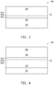
Referring to FIG. 3 , a III-V compound layer 301 is formed over the buffer layer 201. In some embodiments, the III-V compound layer 301 comprises gallium nitride (GaN), or the like. In some embodiments, the III-V compound layer 301 may be epitaxially grown over the buffer layer 201 using similar methods as the buffer layer 103 described above with reference to FIG. 1 , and the description is not repeated herein. In some embodiments where the III-V compound layer 301 comprises GaN, the III-V compound layer 301 may be epitaxially grown by using, for example, MOVPE, during which a gallium-containing precursor and a nitrogen-containing precursor are used. The gallium-containing precursor may include trimethylgallium (TMG), triethylgallium (TEG), other suitable gallium-containing chemicals, a combination thereof, or the like. The nitrogen-containing precursor may include ammonia (NH3), tertiarybutylamine (TBAm), phenyl hydrazine, other suitable nitrogen-containing chemicals, a combination thereof, or the like. In some embodiments, the III-V compound layer 301 has a thickness between about 200 nm and about 5000 nm.
In some embodiments, the III-V compound layer 301 may be doped using suitable dopants. In some embodiments, where the III-V compound layer 301 comprises GaN, the III-V compound layer 301 may be carbon (C) doped or iron (Fe) doped. In some embodiments, the III-V compound layer 301 may be in situ doped while epitaxially growing the III-V compound layer 301. In such embodiments, the epitaxial growing process may further include a carbon-containing precursor or an iron-containing precursor. The carbon-containing precursor may include methane (CH4), ethylene (C2H4), acetylene (C2H2), propane (C3H8), iso-butane (i-C4H10), trimethylamine [N(CH3)3], carbon tetrachloride (CCl4), a combination thereof, or the like. The iron-containing precursor may include Bis(cyclopentadienyl)iron [(C5H5)2Fe], pentacarbonyl iron [(CO)5Fe], the like. In other embodiments, the III-V compound layer 301 may be doped after the formation of the III-V compound layer 301 is completed. In such embodiments, the III-V compound layer 301 may be doped using an implantation method, or the like. In some embodiments, the III-V compound layer 301 is a semi-insulating layer. In some embodiments, the III-V compound layer 301 improves leakage and breakdown performances of the HEMT device 100.
Referring to FIG. 4 , a III-V compound layer 401 is formed over the III-V compound layer 301. In some embodiments, the III-V compound layer 401 comprises a III-V compound, such as gallium nitride (GaN), or the like. In some embodiments, the III-V compound layer 401 may be epitaxially grown using similar method as the III-V compound layer 301 described above with reference to FIG. 3 , and the description is not repeated herein. In some embodiments, the III-V compound layer 401 has a thickness between about 300 nm and about 3000 nm. The III-V compound layer 401 may be undoped. Alternatively, the III-V compound layer 401 is unintentionally doped, such as lightly doped with n-type (or p-type) dopants due to a precursor used for forming the III-V compound layer 401, with no dopant that may cause the III-V compound layer 401 to be n-type or p-type intentionally added.
Referring to FIG. 5 , a III-V compound layer 501 is formed over the III-V compound layer 401. The III-V compound layer 501 may also referred to as a barrier layer or a polarization layer. In some embodiments, the III-V compound layer 501 has a band gap higher than the band gap of the III-V compound layer 401. In such embodiments, the III-V compound layer 501 generates a quantum well within the III-V compound layer 401 near an interface 503 between the III-V compound layer 501 and III-V compound layer 401. The quantum well traps carriers, such as electrons or holes, and forms a channel layer 505 (shown as a dashed line in FIG. 5 ), which is known as a two-dimensional electron gas (2DEG) or a two-dimensional hole gas (2DHG), respectively, in the III-V compound layer 401 near the interface 503. In the following description, a thickness of the dashed line of the channel layer illustrates a carrier concentration within the channel layer 505. The channel layer 505 has high electron mobility partly because the III-V compound layer 401 is undoped or unintentionally doped and the carriers (such as, electrons or holes) can move freely without collision or with substantially reduced collisions with impurities (such as, for example, unintentionally introduced dopants).
In some embodiments, the III-V compound layer 501 comprises AlGaN, or the like. In some embodiments, an aluminum content in the III-V compound layer 501 may be altered relative to a gallium content to alter a polarization strength of the III-V compound layer 501. In some embodiment, the aluminum content x in the III-V compound layer 501 formed of AlxGa1-xN may be between about 0.7 and about 0.6. In some embodiments, the III-V compound layer 501 may be epitaxially grown over the III-V compound layer 401 using MOCVD, MBE, LPE, VPE, MOVPE, SEG, combinations thereof, or the like. In some embodiments where the III-V compound layer 501 comprises AlGaN, the III-V compound layer 501 may be grown by a MOVPE process using an aluminum-containing precursor, a gallium-containing precursor, and a nitrogen-containing precursor. The aluminum-containing precursor may include trimethylaluminum (TMA), triethylaluminium (TEA), other suitable aluminum-containing chemicals, a combination thereof, or the like. The gallium-containing precursor and the nitrogen-containing precursor may be selected from the same candidate precursors used for forming the III-V compound layers 301 and 401 described above with reference to FIGS. 3 and 4 , respectively, and the description is not repeated herein. In some embodiments, the III-V compound layer 501 has a thickness between about 10 nm and about 30 nm.
Referring to FIG. 6A, a III-V compound layer 601 is formed over the III-V compound layer 501. In some embodiments, the III-V compound layer 601 may comprise GaN, p-doped aluminum gallium nitride (p-AlGaN), or the like. In some embodiments, the III-V compound layer 601 may be formed using similar methods as the III-V compound layers 301 and 401, described above with reference to FIGS. 3 and 4 , respectively, and the description is not repeated herein. In some embodiments where the III-V compound layer 601 comprises GaN, the III-V compound layer 601 may be epitaxially grown by using, for example, MOVPE, during which a gallium-containing precursor and a nitrogen-containing precursor are used. The gallium-containing precursor and the nitrogen-containing precursor may be selected from the same candidate precursors used for forming the III-V compound layers 301 and 401 described above with reference to FIGS. 3 and 4 , respectively, and the description is not repeated herein.
In some embodiments, the III-V compound layer 601 is p-doped. In some embodiments where the III-V compound layer 601 comprises GaN, the III-V compound layer 601 may be p-doped using magnesium (Mg), zinc (Zn), a combination thereof, or the like. In some embodiments, the III-V compound layer 601 may be in situ doped while epitaxially growing the III-V compound layer 601. In such embodiments, the MOVPE process may further include a magnesium-containing precursor, a zinc-containing precursor, or a combination thereof. The magnesium-containing precursor may include bis-cyclopentadienyl magnesium (Cp2Mg), bismethylcyclopentadienyl magnesium [(MeCp)2Mg], bisethylcyclopentadienyl magnesium (ECp2Mg), a combination thereof, or the like. The zinc-containing precursor may include diethylzinc (DEZn), or the like. In other embodiments, the III-V compound layer 601 may be doped after the formation of the III-V compound layer 601 is completed. In such embodiments, the III-V compound layer 601 may be doped using an implantation method, or the like. In some embodiments, an annealing process may be performed to activate the dopants. In some embodiments, the III-V compound layer 601 has a thickness between about 10 nm and about 500 nm.
Referring to FIG. 6B, the III-V compound layer 601 is patterned to remove portions of the III-V compound layer 601 over the III-V compound layer 501. In some embodiments, the III-V compound layer 601 may be patterned using suitable photolithography and etching methods. In some embodiments, the patterned III-V compound layer 601 has a width W1 between about 1 μm and about 20 μm. In some embodiments, the patterned III-V compound layer 601 depletes carriers in a channel region 603 of the channel layer 505 (illustrated by absence of the dashed line in the channel region 603 of the channel layer 505) that is located directly below the patterned III-V compound layer 601. Portions of the channel layer 505 on either side of the channel region 603 may form access regions 605, which may also referred to as sourced/drain regions 605. In such embodiments, the channel layer 505 has a non-uniform carrier concentration, with the carriers having a higher concentration in the access regions 605 than in the channel region 603. As described below in greater detail, a gate electrode is formed over the patterned III-V compound layer 601 that allows for tuning the carrier concentration in the channel region 603 of the channel layer 505. Accordingly, the patterned III-V compound layer 601 may be a part of a gate structure formed over the channel region 603 of the channel layer 505. In some embodiments, by forming the III-V compound layer 601 over the III-V compound layer 501 that depletes carriers in the channel region 603 of the channel layer 505, a threshold voltage (Vth) of the HEMT device 100 may be increased.
Referring to FIG. 7 , a passivation layer 701 is formed over the III-V compound layers 501 and 601. In some embodiments, the passivation layer 701 may comprise silicon oxide, silicon nitride, silicon oxynitride, a combination thereof, or the like, and may be formed using chemical vapor deposition (CVD), atomic layer deposition (ALD), a combination thereof, or the like. In some embodiments, the passivation layer 701 may have a thickness between about 1 μm and about 10 μm.
Referring to FIG. 8 , the passivation layer 701 is patterned to expose portions of the III-V compound layer 501 not covered by the III-V compound layer 601. Furthermore, the passivation layer 701 is patterned such that a remaining portion of the passivation layer 701 covers a top surface and sidewall of the III-V compound layer 601. In some embodiments, the remaining portion of the passivation layer 701 protects the III-V compound layer 601 from subsequent process steps. In some embodiments, the passivation layer 701 is patterned using suitable photolithography and etching methods.
Referring to FIG. 9 , a III-V compound layer 901 is formed over the exposed portions of the III-V compound layer 501 on either side of the III-V compound layer 601. In some embodiments, the III-V compound layer 901 has a band gap higher than the band gap of the III-V compound layer 401. The III-V compound layer 901 may also be referred to as a barrier layer or a polarization layer. In some embodiments, the III-V compound layer 901 may comprise AlGaN, or the like. In some embodiments, an aluminum content in the III-V compound layer 901 may be altered relative to a gallium content to alter a polarization strength of the III-V compound layer 901. In some embodiments, the III-V compound layer 901 may have a greater aluminum content than the III-V compound layer 501. In such embodiments, the III-V compound layer 901 has a higher polarization strength than the III-V compound layer 501. In some embodiment, the aluminum content y in the III-V compound layer 901 formed of AlyGa1-yN may be between about 0.7 and about 0.6. In some embodiment, a ratio of the aluminum content y in the III-V compound layer 901 formed of AlyGa1-yN over the aluminum content x in the III-V compound layer 501 formed of AlxGa1-xN is between about 1.1 and about 2.5.
In some embodiments, by forming the III-V compound layer 901 over the III-V compound layer 501, the carrier concentration in the channel layer 505 is further altered. In some embodiments, the carrier concentration in the channel layer 505 is altered such that the carrier concentration in the access regions 605 of the channel layer 505 directly below the III-V compound layer 901 is greater than the carrier concentration in the access regions 605 of the channel layer 505 directly below the passivation layer 701. By increasing the carrier concentration in the access regions 605 of the channel layer 505, an on-resistance (dRon) of the HEMT device 100 is lowered.
The III-V compound layers 501 and 901 form a multi-barrier layer structure over the III-V compound layer 401. In the illustrated embodiment, the multi-barrier layer structure comprises two layers (such as the III-V compound layers 501 and 901). In other embodiments, the multi-barrier layer structure may comprise more than two layers according to design specifications of the HEMT device 100. By not forming the III-V compound layer 901 over the channel region 603 of the channel layer 505, low carrier concentration in the channel region 603 is achieved, which results in the high threshold voltage (Vth). In some embodiments, the threshold voltage (Vth) is between about −6 V and about +6 V.
Referring further to FIG. 9 , the III-V compound layer 901 is epitaxially grown over the III-V compound layer 501 using MOCVD, MBE, LPE, VPE, MOVPE, SEG, combinations thereof, or the like. In some embodiments, the III-V compound layer 901 is selectively grown over the exposed portions of the III-V compound layer 501, such that no portion of the III-V compound layer 901 is formed over the passivation layer 701. In some embodiments where the III-V compound layer 901 comprises AlGaN, the III-V compound layer 901 may be epitaxially grown using an aluminum-containing precursor, a gallium-containing precursor, and a nitrogen-containing precursor. The aluminum-containing precursor, the gallium-containing precursor and the nitrogen-containing precursor may be selected from the same candidate precursors used for forming the III-V compound layer 501 described above with reference to FIG. 5 , and the description is not repeated herein. In some embodiments, the III-V compound layer 901 has a thickness between about 1 nm and about 50 nm.
In some embodiments where the III-V compound layer 901 comprises AlGaN, a method of forming the III-V compound layer 901 includes introducing the substrate 101 with the passivation layer 701 and the III-V compound layers 501 and 601 formed thereon in a process chamber and ramping up a process temperature to a target temperature before introducing the aluminum-containing precursor, the gallium-containing precursor, and the nitrogen-containing precursor into the process chamber. In some embodiments, the process temperature is ramped up to the target temperature during a first time interval between about 1 min and about 300 min. In some embodiments, the target temperature is between about 700° C. and about 1100° C. By tuning the target temperature to be less than about 816° C., decomposition of the exposed portions of the III-V compound layer 501 may be reduced or avoided. Furthermore, a root-mean-square roughness of a topmost surface of the III-V compound layer 501 is not substantially increased. Accordingly, after forming the III-V compound layer 901 over the III-V compound layer 501, a well-defined smooth interface is formed between the III-V compound layer 901 and the III-V compound layer 501. By forming the well-defined smooth interface between the III-V compound layers 901 and 501, carrier trapping may be avoided at the interface that results in a low dynamical on-resistance (dRon) of the HEMT device 100. In some embodiment, a root-mean-square (RMS) roughness of the interface between the III-V compound layers 901 and 501 is between about 0.5 nm and about 10 nm.
In some embodiments, after process temperature reaches the target temperature, the aluminum-containing precursor, the gallium-containing precursor, and the nitrogen-containing precursor are introduced in the process chamber. In some embodiments, a flow rate of the aluminum-containing precursor is between about 10 sccm and about 1000 sccm. In some embodiments, a flow rate of the gallium-containing precursor is between about 10 sccm and about 1000 sccm. In some embodiments, a flow rate of the nitrogen-containing precursor is between about 100 sccm and about 100000 sccm. In some embodiments, the aluminum-containing precursor, the gallium-containing precursor, and the nitrogen-containing precursor are flown into the process chamber during a growth time between about 1 s and about 387 s. In some embodiments, the growth time is tuned until a desired thickness of the III-V compound layer 901 is achieved.
Referring to FIG. 10 , after the formation of the III-V compound layer 901 is completed, the passivation layer 701 is removed. In some embodiments, the passivation layer 701 is removed using a selective wet etching process, a selective dry etching process, a combination thereof, or the like. After removing the passivation layer 701, a portion of the topmost surface of the III-V compound layer 501 is exposed between the III-V compound layer 601 and the III-V compound layer 901.
Referring to FIG. 11 , a passivation layer 1101 is formed over the III-V compound layers 501, 601 and 901. In some embodiments, the passivation layer 1101 may be formed using similar materials and methods as the passivation layer 701 described above with reference to FIG. 7 , and the description is not repeated herein. In some embodiments, the passivation layer 1101 has a thickness between about 1 μm and about 20 μm.
Referring to FIG. 12 , the passivation layer 1101 and the III-V compound layers 501 and 901 are patterned to form openings 1201. The openings 1201 extend through the passivation layer 1101 and the III-V compound layer 901, and into the III-V compound layer 501, such that portions of the III-V compound layer 501 having a thickness T remain directly below the openings 1201. In some embodiments, the thickness T is between about 2 nm and about 4 nm. In some embodiments, the passivation layer 1101 and the III-V compound layers 501 and 901 are patterned using a suitable photolithography and etching processes. The suitable etching process may include one or more wet etching processes, one or more dry etching processes, a combination thereof, or the like. In other embodiments, the patterning process may pattern only the passivation layer 1101, such that the openings 1201 expose the topmost surface of the III-V compound layer 901. In yet other embodiments, the patterning process may pattern the passivation layer 1101 and the III-V compound layers 501 and 901, such that the openings 1201 expose the topmost surface of the III-V compound layer 401.
Referring to FIG. 13 , source/drain electrodes 1301 are formed in the openings 1201 (see FIG. 12 ). In some embodiments, the source/drain electrodes 1301 are formed by a deposition process followed by lithography and etching processes. In other embodiments, the source/drain electrodes 1301 are formed by forming a patterned sacrificial layer (such as, for example, a photoresist layer) over the passivation layer 1101, such that openings in the patterned sacrificial layer are aligned with respective ones of the openings 1201, followed by a deposition process and a lift-off process to remove the patterned sacrificial layer.
In some embodiments, the source/drain electrodes 1301 include one or more conductive materials. For example, the source/drain electrodes 1301 may comprise Ti, Co, Ni, W, Pt, Ta, Pd, Mo, TiN, an AlCu alloy, alloys thereof, or the like. In some embodiments, each of the source/drain electrodes 1301 includes a bottom Ti/TiN layer, an AlCu layer overlying the bottom Ti/TiN layer, and a top Ti layer overlying the AlCu layer. The formation methods of the one or more conductive materials include ALD, physical vapor deposition (PVD), electrochemical plating, electroless plating, a combination thereof, or the like. In some embodiments, a thermal annealing process is applied to the source/drain electrodes 1301 to react with the III-V compound layers 501 and 901 to form an inter-metallic compound (not shown) at interfaces between the source/drain electrodes 1301 and the III-V compound layers 501 and 901. The inter-metallic compound may provide more effective electrical connection to the access regions 605 of the channel layer 505.
Referring to FIG. 14 , a passivation layer 1401 is formed over the passivation layer 1101 and the source/drain electrodes 1301. In some embodiments, the passivation layer 1401 may be formed using similar materials and methods as the passivation layer 701 described above with reference to FIG. 7 , and the description is not repeated herein. In some embodiments, the passivation layers 1101 and 1401 comprise a same material. In such embodiments, an interface between the passivation layers 1101 and 1401 may not be detectable. In other embodiments, the passivation layers 1101 and 1401 comprise different materials. In some embodiments, the passivation layer 1401 has a thickness between about 1 μm and about 20 μm.
Referring to FIG. 15 , the passivation layers 1101 and 1401 are patterned to form an opening 1501. The opening 1501 exposes a topmost surface of the III-V compound layer 601. In some embodiments, the passivation layers 1101 and 1401 are patterned using a suitable photolithography and etching processes. The suitable etching process may include one or more wet etching processes, one or more dry etching processes, a combination thereof, or the like.
Referring to FIG. 16 , a gate electrode 1601 is formed in the opening 1501 (see FIG. 15 ) over the III-V compound layer 601. In some embodiments, the gate electrode 1601 is formed by a deposition process followed by lithography and etching processes. In other embodiments, the gate electrode 1601 is formed by forming a patterned sacrificial layer (such as, for example, a photoresist layer) over the passivation layer 1401, such that an opening in the patterned sacrificial layer is aligned with the opening 1501, followed by a deposition process and a lift-off process to remove the patterned sacrificial layer.
In some embodiments, the gate electrode 1601 includes one or more conductive materials. In some embodiments, the gate electrode 1601 is formed of tantalum or titanium containing materials such as TaC, TaN, TiN, TaAlN, TaSiN, TaCN, a combination thereof, or the like. These metal-containing materials may be in the form of metal carbides, metal nitrides, or conductive metal oxides. Other embodiments may utilize other types of metals, such as W, Ni, Au, Cu, Ta, Ti, Ag, Al, TiAl, Mn, WN, Ru, Zr, a combination thereof, or the like. The formation methods of the gate electrode 1601 include ALD, PVD, MOCVD, a combination thereof, or the like. The gate electrode 1601 may further include two or more layers for a composite gate structure. Although FIG. 16 illustrate the gate electrode 1601 being formed directly on the topmost surface of the III-V compound layer 601, various intermediary layers (such as, for example, a gate dielectric, interfacial layers, work/function metals, or the like) may be formed between the gate electrode 1601 and the III-V compound layer 601.
Referring to FIG. 17 , an interlayer dielectric (ILD) 1701 is formed over the gate electrode 1601 and the passivation layer 1401. In some embodiments, the ILD 1701 is formed of a dielectric material, such as Phospho-Silicate Glass (PSG), Boro-Silicate Glass (BSG), Boron-Doped Phospho-Silicate Glass (BPSG), undoped Silicate Glass (USG), a combination thereof, or the like, and may be deposited by any suitable method, such as CVD, plasma enhanced CVD (PECVD), a spin-on-glass process, a combination thereof, or the like. In some embodiments, a planarization process, such as a chemical mechanical polishing (CMP) process, may be performed to planarize a topmost surface of the ILD 1701.
In some embodiments, the ILD 1701 and the passivation layer 1401 are patterned to form openings 1703 and 1705. In some embodiments, the ILD 1701 and the passivation layer 1401 are patterned using a suitable photolithography and etching processes. The suitable etching process may include one or more wet etching processes, one or more dry etching processes, a combination thereof, or the like. The openings 1703 and 1705 may all be formed simultaneously in a same process, or in separate processes. The openings 1703 extend through the ILD 1701 and the passivation layer 1401 and expose topmost surfaces of the source/drain electrodes 1301. The opening 1705 extends through the ILD 1701 and exposes a topmost surface of the gate electrode 1601.
Referring to FIG. 18 , contact plugs 1801 are formed in the openings 1703 (see FIG. 17 ) and a contact plug 1803 is formed in the opening 1705 (see FIG. 17 ). In some embodiments, a liner, such as a diffusion barrier layer, an adhesion layer, or the like, and a conductive material are deposited in the openings 1703 and 1705. The liner may include titanium, titanium nitride, tantalum, tantalum nitride, a combination thereof, or the like. Subsequently, the openings 1703 and 1705 are filled with a conductive material. The conductive material may be copper, a copper alloy, silver, gold, tungsten, aluminum, nickel, a combination thereof, or the like. A planarization process, such as a CMP process, may be performed to remove excess materials from a top surface of the ILD 1701. The remaining portions of the liner and the conductive material form the contact plugs 1801 and 1803. The contact plugs 1801 are physically and electrically coupled to the source/drain electrodes 1301 and the contact plug 1803 is physically and electrically coupled to the gate electrode 1601. While the contact plugs 1801 are depicted in FIG. 18 in a same cross-section as the contact plug 1803, this depiction is for the purposes of illustration only and, in other embodiments, the contact plugs 1801 may be disposed in a different cross-section than the contact plug 1803.
FIG. 19 is a flow diagram illustrating a method 1900 of forming a HEMT device in accordance with some embodiments. The method 1900 starts with step 1901, where a first III-V compound layer (such as, for example, the III-V compound layer 401 illustrated in FIG. 4 ) is formed over a substrate (such as, for example, the substrate 101 illustrated in FIG. 4 ) as described above with reference to FIG. 4 . In step 1903, a second III-V compound layer (such as, for example, the III-V compound layer 501 illustrated in FIG. 5 ) is formed over the first III-V compound layer as described above with reference to FIG. 5 . In step 1905, a third III-V compound layer (such as, for example, the III-V compound layer 601 illustrated in FIG. 6B) is formed over the second III-V compound layer as described above with reference to FIGS. 6A and 6B. In step 1907, a passivation layer (such as, for example, the passivation layer 701 illustrated in FIG. 8 ) is formed over a topmost surface and sidewalls of the third III-V compound layer as described above with reference to FIGS. 7 and 8 . In step 1909, a fourth III-V compound layer (such as, for example, the III-V compound layer 901 illustrated in FIG. 9 ) is formed over the second III-V compound layer as described above with reference to FIG. 9 . In step 1911, the passivation layer is removed as described above with reference to FIG. 10 . In step 1913, source/drain electrodes (such as, for example, the source/drain electrodes 1301 illustrated in FIG. 13 ) are formed as described above with reference to FIGS. 11-13 . In step 1915, a gate electrode (such as, for example, the gate electrode 1601 illustrated in FIG. 16 ) is formed as described above with reference to FIGS. 14-16 . In step 1917, contact plugs (such as, for example, the contact plugs 1801 and 1803 illustrated in FIG. 18 ) are formed as described above with reference to FIGS. 17 and 18 .
In accordance with an embodiment, a method includes forming a first III-V compound layer over a substrate. A second III-V compound layer is formed over the first III-V compound layer. The second III-V compound layer has a greater band gap than the first III-V compound layer. A third III-V compound layer is formed over the second III-V compound layer. The third III-V compound layer and the first III-V compound layer comprise a same III-V compound. A passivation layer is formed along a topmost surface and sidewalls of the third III-V compound layer. A fourth III-V compound layer is formed over the second III-V compound layer. The fourth III-V compound layer has a greater band gap than the first III-V compound layer. In an embodiment, forming the passivation layer includes blanket depositing a dielectric material over the second III-V compound layer and the third III-V compound layer, and patterning the dielectric material to expose a topmost surface of the second III-V compound layer. A remaining portion of the dielectric material forms the passivation layer. In an embodiment, the third III-V compound layer is a p-doped layer. In an embodiment, forming the fourth III-V compound layer includes: introducing the substrate into a process chamber; ramping up a process temperature to a target temperature; and after ramping up the process temperature to the target temperature, introducing precursors into the process chamber. In an embodiment, the target temperature is between about 700° C. and about 950° C. In an embodiment, the second III-V compound layer is not intentionally doped. In an embodiment, forming the fourth III-V compound layer over the second III-V compound layer includes selectively epitaxially growing the fourth III-V compound layer over the second III-V compound layer.
In accordance with another embodiment, a method includes forming a GaN layer over a substrate. A first AlGaN layer is formed over the GaN layer. A p-doped GaN layer is formed over the first AlGaN layer. A dielectric material is blanket deposited over the p-doped GaN layer and the first AlGaN layer. A portion of the dielectric material is removed from over a topmost surface of the first AlGaN layer. A remaining portion of the dielectric material extending along a topmost surface and sidewalls of the p-doped GaN layer forms a passivation layer. A second AlGaN layer is formed over the first AlGaN layer. The second AlGaN layer has a greater aluminum content than the first AlGaN layer. In an embodiment, forming the second AlGaN layer includes: introducing the substrate into a process chamber; ramping up a process temperature to a target temperature; and after ramping up the process temperature to the target temperature, introducing an aluminum precursor, a gallium precursor and a nitrogen precursor into the process chamber. In an embodiment, the target temperature is between about 700° C. and about 950° C. In an embodiment, the p-doped GaN layer is in situ doped. In an embodiment, the first AlGaN layer includes AlxGa1-xN, the second AlGaN layer includes AlyGa1-yN, and a ratio y/x is between about 1.1 and about 2.5. In an embodiment, the GaN layer is not intentionally doped. In an embodiment, the method further includes, after forming the second AlGaN layer, removing the passivation layer.
In accordance with yet another embodiment, a device includes a substrate, a GaN layer over the substrate, a first AlGaN layer over the GaN layer, and a p-doped GaN layer over the first AlGaN layer. A width of the p-doped GaN layer is less than a width of the first AlGaN layer. The device further includes a second AlGaN layer over the first AlGaN layer. The second AlGaN layer has a greater aluminum content than the first AlGaN layer. In an embodiment, the first AlGaN layer includes AlxGa1-xN, the second AlGaN layer includes AlyGa1-yN, and a ratio y/x is between about 1.1 and about 2.5. In an embodiment, the GaN layer is an un-doped layer. In an embodiment, the device further includes a passivation layer over the p-doped GaN layer and the second AlGaN layer. The passivation layer extends along a sidewall of the p-doped GaN layer and a sidewall of the second AlGaN layer. In an embodiment, the device further includes a gate electrode extending through the passivation layer and physically contacting a topmost surface of the p-doped GaN layer. In an embodiment, the device further includes a graded AlGaN buffer layer between the substrate and the GaN layer.
In accordance with yet another embodiment, a device includes a substrate, a first III-V compound layer over the substrate, a second III-V compound layer over the first III-V compound layer, a third III-V compound layer over the second III-V compound layer, a fourth III-V compound layer over the second III-V compound layer, and a passivation layer over the third III-V compound layer and the fourth III-V compound layer. The second III-V compound layer has a greater band gap than the first III-V compound layer. The third III-V compound layer and the first III-V compound layer include a same III-V compound. The fourth III-V compound layer has a greater band gap than the first III-V compound layer. A portion of the passivation layer extends between the third III-V compound layer and the fourth III-V compound layer, and is in physical contact with the second III-V compound layer. In an embodiment, the device further includes a source/drain electrode extending through the passivation layer, the fourth III-V compound layer, and into the second III-V compound layer. In an embodiment, the device further includes a gate electrode extending through the passivation layer and being in physical contact with the third III-V compound layer. In an embodiment, the first III-V compound layer includes GaN. In an embodiment, the second III-V compound layer includes AlGaN. In an embodiment, the third III-V compound layer includes p-doped GaN. In an embodiment, the fourth III-V compound layer includes AlGaN.
In accordance with yet another embodiment, a device includes a first semiconductor layer over a substrate, a second semiconductor layer over the first semiconductor layer, a third semiconductor layer over the second semiconductor layer, a fourth semiconductor layer over the second semiconductor layer, a passivation layer over the third semiconductor layer and the fourth semiconductor layer, and a source/drain electrode extending through the passivation layer, the fourth semiconductor layer, and into the second semiconductor layer. The first semiconductor layer includes a first III-V compound. The second semiconductor layer includes a second III-V compound different from the first III-V compound. The third semiconductor layer includes a p-doped first III-V compound. The third semiconductor layer is interposed between two disconnected portions of the fourth semiconductor layer. The fourth semiconductor layer includes a third III-V compound. A bottom surface of the passivation layer is lower than a top surface of the third semiconductor layer and a top surface of the fourth semiconductor layer. In an embodiment, the first III-V compound includes GaN. In an embodiment, the second III-V compound and the third III-V compound include AlGaN. In an embodiment, the device further includes a gate electrode extending through the passivation layer and being in physical contact with the third semiconductor layer. In an embodiment, a top surface of the gate electrode is above a top surface of the source/drain electrode. In an embodiment, the passivation layer is in physical contact with the second semiconductor layer. In an embodiment, a top surface of the source/drain electrode is above a top surface of the passivation layer.
The foregoing outlines features of several embodiments so that those skilled in the art may better understand the aspects of the present disclosure. Those skilled in the art should appreciate that they may readily use the present disclosure as a basis for designing or modifying other processes and structures for carrying out the same purposes and/or achieving the same advantages of the embodiments introduced herein. Those skilled in the art should also realize that such equivalent constructions do not depart from the spirit and scope of the present disclosure, and that they may make various changes, substitutions, and alterations herein without departing from the spirit and scope of the present disclosure.

Claims (20)

What is claimed is:
1. A device comprising:
a substrate;
a first III-V compound layer over the substrate;
a second III-V compound layer over the first III-V compound layer, the second III-V compound layer having a greater band gap than the first III-V compound layer;
a third III-V compound layer over the second III-V compound layer, the third III-V compound layer and the first III-V compound layer comprising a same III-V compound;
a fourth III-V compound layer over the second III-V compound layer, a bottom surface of the third III-V compound layer and a bottom surface of the fourth III-V compound layer being in physical contact with a top surface of the second III-V compound layer, the fourth III-V compound layer having a greater band gap than the first III-V compound layer; and
a passivation layer over the third III-V compound layer and the fourth III-V compound layer, a portion of the passivation layer extending between the third III-V compound layer and the fourth III-V compound layer, and being in physical contact with the second III-V compound layer.
2. The device of claim 1, further comprising a source/drain electrode extending through the passivation layer, the fourth III-V compound layer, and into the second III-V compound layer.
3. The device of claim 1, further comprising a gate electrode extending through the passivation layer and being in physical contact with the third III-V compound layer.
4. The device of claim 1, wherein the first III-V compound layer comprises GaN.
5. The device of claim 1, wherein the second III-V compound layer comprises AlGaN.
6. The device of claim 1, wherein the third III-V compound layer comprises p-doped GaN.
7. The device of claim 1, wherein the fourth III-V compound layer comprises AlGaN.
8. A device comprising:
a first semiconductor layer over a substrate, the first semiconductor layer comprising a first III-V compound;
a second semiconductor layer over the first semiconductor layer, the second semiconductor layer comprising a second III-V compound different from the first III-V compound;
a third semiconductor layer over the second semiconductor layer, the third semiconductor layer comprising a p-doped first III-V compound;
a fourth semiconductor layer over the second semiconductor layer, the third semiconductor layer being interposed between two disconnected portions of the fourth semiconductor layer, the third semiconductor layer being spaced apart from the two disconnected portions of the fourth semiconductor layer, the fourth semiconductor layer comprising a third III-V compound;
a passivation layer over the third semiconductor layer and the fourth semiconductor layer, a bottom surface of the passivation layer being lower than a top surface of the third semiconductor layer and a top surface of the fourth semiconductor layer; and
a source/drain electrode extending through the passivation layer, the fourth semiconductor layer, and into the second semiconductor layer.
9. The device of claim 8, wherein the first III-V compound comprises GaN.
10. The device of claim 8, wherein the second III-V compound and the third III-V compound comprise AlGaN.
11. The device of claim 8, further comprising a gate electrode extending through the passivation layer and being in physical contact with the third semiconductor layer.
12. The device of claim 11, wherein a top surface of the gate electrode is above a top surface of the source/drain electrode.
13. The device of claim 8, wherein the passivation layer is in physical contact with the second semiconductor layer.
14. The device of claim 8, wherein a top surface of the source/drain electrode is above a top surface of the passivation layer.
15. A device comprising:
a substrate;
a first GaN layer over the substrate;
a first AlGaN layer over the first GaN layer;
a p-doped second GaN layer over the first AlGaN layer, a width of the p-doped second GaN layer being less than a width of the first AlGaN layer; and
a second AlGaN layer over the first AlGaN layer, the second AlGaN layer having a greater aluminum content than the first AlGaN layer, wherein a sidewall of the p-doped second GaN layer faces a sidewall of the second AlGaN layer.
16. The device of claim 15, wherein the first AlGaN layer comprises AlxGa1-xN, wherein the second AlGaN layer comprises AlyGa1-yN, and wherein a ratio y/x is between about 1.1 and about 2.5.
17. The device of claim 15, wherein the first GaN layer is an un-doped layer.
18. The device of claim 15, further comprising a passivation layer over the p-doped second GaN layer and the second AlGaN layer, the passivation layer extending along the sidewall of the p-doped second GaN layer and the sidewall of the second AlGaN layer.
19. The device of claim 18, further comprising a gate electrode extending through the passivation layer and physically contacting a topmost surface of the p-doped second GaN layer.
20. The device of claim 15, further comprising a graded AlGaN buffer layer between the substrate and the first GaN layer.
US17/225,482 2018-06-29 2021-04-08 High electron mobility transistor (HEMT) device and method of forming same Active US11522067B2 (en)

Priority Applications (1)

Application Number Priority Date Filing Date Title
US17/225,482 US11522067B2 (en) 2018-06-29 2021-04-08 High electron mobility transistor (HEMT) device and method of forming same

Applications Claiming Priority (3)

Application Number Priority Date Filing Date Title
US201862691937P 2018-06-29 2018-06-29
US16/414,879 US11011614B2 (en) 2018-06-29 2019-05-17 High electron mobility transistor (HEMT) device and method of forming same
US17/225,482 US11522067B2 (en) 2018-06-29 2021-04-08 High electron mobility transistor (HEMT) device and method of forming same

Related Parent Applications (1)

Application Number Title Priority Date Filing Date
US16/414,879 Division US11011614B2 (en) 2018-06-29 2019-05-17 High electron mobility transistor (HEMT) device and method of forming same

Publications (2)

Publication Number Publication Date
US20210226040A1 US20210226040A1 (en) 2021-07-22
US11522067B2 true US11522067B2 (en) 2022-12-06

Family

ID=68886151

Family Applications (2)

Application Number Title Priority Date Filing Date
US16/414,879 Active US11011614B2 (en) 2018-06-29 2019-05-17 High electron mobility transistor (HEMT) device and method of forming same
US17/225,482 Active US11522067B2 (en) 2018-06-29 2021-04-08 High electron mobility transistor (HEMT) device and method of forming same

Family Applications Before (1)

Application Number Title Priority Date Filing Date
US16/414,879 Active US11011614B2 (en) 2018-06-29 2019-05-17 High electron mobility transistor (HEMT) device and method of forming same

Country Status (5)

Country Link
US (2) US11011614B2 (en)
KR (1) KR102194068B1 (en)
CN (1) CN110660844B (en)
DE (1) DE102019113589A1 (en)
TW (1) TWI717773B (en)

Families Citing this family (9)

* Cited by examiner, † Cited by third party
Publication number Priority date Publication date Assignee Title
US11335799B2 (en) * 2015-03-26 2022-05-17 Chih-Shu Huang Group-III nitride semiconductor device and method for fabricating the same
KR20210089486A (en) 2020-01-08 2021-07-16 삼성전자주식회사 Apparatus and method for securely managing keys
KR20210089485A (en) 2020-01-08 2021-07-16 삼성전자주식회사 Apparatus and method for authentication of software
CN111684606A (en) * 2020-04-22 2020-09-18 英诺赛科(珠海)科技有限公司 Semiconductor device having multi-channel heterostructure and method of fabricating the same
CN111602248A (en) * 2020-04-22 2020-08-28 英诺赛科(珠海)科技有限公司 Semiconductor device having multi-channel heterostructure and method of fabricating the same
US11677002B2 (en) * 2020-09-16 2023-06-13 Vanguard International Semiconductor Corporation Semiconductor structure
TWI780513B (en) * 2020-11-13 2022-10-11 國立中山大學 P-GaN HIGH ELECTRON MOBILITY TRANSISTOR
TWI763272B (en) * 2021-01-22 2022-05-01 合晶科技股份有限公司 Enhancement mode transistor and method for manufacturing the same
US20220376098A1 (en) * 2021-05-20 2022-11-24 Wolfspeed, Inc. Field effect transistor with selective modified access regions

Citations (4)

* Cited by examiner, † Cited by third party
Publication number Priority date Publication date Assignee Title
US20060226442A1 (en) * 2005-04-07 2006-10-12 An-Ping Zhang GaN-based high electron mobility transistor and method for making the same
JP2010135641A (en) 2008-12-05 2010-06-17 Panasonic Corp Field effect transistor and manufacturing method thereof
US20140191240A1 (en) * 2013-01-04 2014-07-10 Taiwan Semiconductor Manufacturing Company, Ltd. High Electron Mobility Transistor and Method of Forming the Same
US20200220004A1 (en) * 2017-09-29 2020-07-09 Intel Corporation Group iii-nitride (iii-n) devices with reduced contact resistance and their methods of fabrication

Family Cites Families (9)

* Cited by examiner, † Cited by third party
Publication number Priority date Publication date Assignee Title
JP3416051B2 (en) * 1998-03-18 2003-06-16 日本電信電話株式会社 Method for manufacturing group III-V compound semiconductor device
CN100461469C (en) * 2000-12-18 2009-02-11 三星电机株式会社 GaN-base III-V group nitride light emitting diode and method for manufacturing same
CN101449366A (en) * 2006-06-23 2009-06-03 国际商业机器公司 Buried channel mosfet using iii-v compound semiconductors and high k gate dielectrics
JP4968747B2 (en) * 2009-02-03 2012-07-04 シャープ株式会社 III-V compound semiconductor device
US9373689B2 (en) * 2012-12-28 2016-06-21 Taiwan Semiconductor Manufacturing Company, Ltd. High electron mobility transistor and method of forming the same
WO2018004607A1 (en) * 2016-06-30 2018-01-04 Intel Corporation Co-integration of gan and self-aligned thin body group iv transistors
US10923584B2 (en) * 2016-07-01 2021-02-16 Intel Corporation Graded channels for high frequency III-N transistors
TWI767741B (en) * 2016-08-23 2022-06-11 美商克若密斯股份有限公司 Electronic power devices integrated with an engineered substrate
TWI798187B (en) * 2016-10-11 2023-04-11 日本商出光興產股份有限公司 Structure, manufacturing method thereof, semiconductor element, and electronic circuit

Patent Citations (5)

* Cited by examiner, † Cited by third party
Publication number Priority date Publication date Assignee Title
US20060226442A1 (en) * 2005-04-07 2006-10-12 An-Ping Zhang GaN-based high electron mobility transistor and method for making the same
JP2010135641A (en) 2008-12-05 2010-06-17 Panasonic Corp Field effect transistor and manufacturing method thereof
US20110227093A1 (en) 2008-12-05 2011-09-22 Panasonic Corporation Field effect transistor and method of manufacturing the same
US20140191240A1 (en) * 2013-01-04 2014-07-10 Taiwan Semiconductor Manufacturing Company, Ltd. High Electron Mobility Transistor and Method of Forming the Same
US20200220004A1 (en) * 2017-09-29 2020-07-09 Intel Corporation Group iii-nitride (iii-n) devices with reduced contact resistance and their methods of fabrication

Non-Patent Citations (3)

* Cited by examiner, † Cited by third party
Title
Chiu, H.C. et al., "High-Performance Normally Off p-GaN Gate HEMT With Composite AIN/A10.17Ga0.83N/AI0.3 Ga0.7N Barrier Layers Design," Journal of the Electron Devices Society, Jan. 2018, vol. 6, pp. 201-206.
Suh C.S. et al., "p-GaN/AlGaN/GaN Enhancement-Mode HEMTs", 64th Device Research Conference, Jun. 26-28, 2006, 3 pages.
Yang Yibin et al., "Effect of Compositionally Graded AlGaN Buffer Layer Grown by Different Functions of Trimethylaluminum Flow Rates on the Properties of GaN on Si (111) Substrates," Elsevier, Journal of Crystal Growth 376, 2013, pp. 23-27.

Also Published As

Publication number Publication date
KR20200002691A (en) 2020-01-08
TWI717773B (en) 2021-02-01
DE102019113589A1 (en) 2020-01-02
US20210226040A1 (en) 2021-07-22
KR102194068B1 (en) 2020-12-23
TW202006951A (en) 2020-02-01
CN110660844A (en) 2020-01-07
US20200006522A1 (en) 2020-01-02
US11011614B2 (en) 2021-05-18
CN110660844B (en) 2022-11-04

Similar Documents

Publication Publication Date Title
US11522067B2 (en) High electron mobility transistor (HEMT) device and method of forming same
US11804538B2 (en) Method of forming a high electron mobility transistor
US10790375B2 (en) High electron mobility transistor
US10134867B2 (en) Method for fabricating semiconductor device
US9899493B2 (en) High electron mobility transistor and method of forming the same
US9793371B2 (en) Method of forming a high electron mobility transistor
US9236465B2 (en) High electron mobility transistor and method of forming the same
CN115458597B (en) Nitride-based semiconductor device and method of manufacturing the same
WO2023197251A1 (en) Nitride-based semiconductor device and method for manufacturing the same
CN113451403A (en) High electron mobility transistor and manufacturing method thereof

Legal Events

Date Code Title Description
FEPP Fee payment procedure

Free format text: ENTITY STATUS SET TO UNDISCOUNTED (ORIGINAL EVENT CODE: BIG.); ENTITY STATUS OF PATENT OWNER: LARGE ENTITY

STPP Information on status: patent application and granting procedure in general

Free format text: APPLICATION DISPATCHED FROM PREEXAM, NOT YET DOCKETED

STPP Information on status: patent application and granting procedure in general

Free format text: DOCKETED NEW CASE - READY FOR EXAMINATION

STPP Information on status: patent application and granting procedure in general

Free format text: NON FINAL ACTION MAILED

STPP Information on status: patent application and granting procedure in general

Free format text: RESPONSE TO NON-FINAL OFFICE ACTION ENTERED AND FORWARDED TO EXAMINER

STPP Information on status: patent application and granting procedure in general

Free format text: NOTICE OF ALLOWANCE MAILED -- APPLICATION RECEIVED IN OFFICE OF PUBLICATIONS

STPP Information on status: patent application and granting procedure in general

Free format text: PUBLICATIONS -- ISSUE FEE PAYMENT VERIFIED

STCF Information on status: patent grant

Free format text: PATENTED CASE