US11515480B2 - Organic light emitting device - Google Patents
Organic light emitting device Download PDFInfo
- Publication number
- US11515480B2 US11515480B2 US16/721,777 US201916721777A US11515480B2 US 11515480 B2 US11515480 B2 US 11515480B2 US 201916721777 A US201916721777 A US 201916721777A US 11515480 B2 US11515480 B2 US 11515480B2
- Authority
- US
- United States
- Prior art keywords
- carbon atoms
- group
- layer
- organic light
- emitting device
- Prior art date
- Legal status (The legal status is an assumption and is not a legal conclusion. Google has not performed a legal analysis and makes no representation as to the accuracy of the status listed.)
- Active, expires
Links
- 150000001875 compounds Chemical class 0.000 claims abstract description 63
- 230000005525 hole transport Effects 0.000 claims abstract description 51
- 125000004432 carbon atom Chemical group C* 0.000 claims description 76
- 239000000126 substance Substances 0.000 claims description 50
- 239000010408 film Substances 0.000 claims description 27
- 239000011368 organic material Substances 0.000 claims description 25
- 238000002347 injection Methods 0.000 claims description 23
- 239000007924 injection Substances 0.000 claims description 23
- 125000003118 aryl group Chemical group 0.000 claims description 20
- 125000000217 alkyl group Chemical group 0.000 claims description 19
- 239000010409 thin film Substances 0.000 claims description 19
- 125000001424 substituent group Chemical group 0.000 claims description 13
- UJOBWOGCFQCDNV-UHFFFAOYSA-N 9H-carbazole Chemical compound C1=CC=C2C3=CC=CC=C3NC2=C1 UJOBWOGCFQCDNV-UHFFFAOYSA-N 0.000 claims description 12
- 125000001072 heteroaryl group Chemical group 0.000 claims description 11
- 125000005843 halogen group Chemical group 0.000 claims description 9
- 125000003545 alkoxy group Chemical group 0.000 claims description 8
- 229910052805 deuterium Inorganic materials 0.000 claims description 8
- 125000003342 alkenyl group Chemical group 0.000 claims description 7
- 125000000304 alkynyl group Chemical group 0.000 claims description 7
- 125000004104 aryloxy group Chemical group 0.000 claims description 7
- 125000004431 deuterium atom Chemical group 0.000 claims description 7
- 229910052760 oxygen Inorganic materials 0.000 claims description 7
- 229910052717 sulfur Inorganic materials 0.000 claims description 6
- 230000004888 barrier function Effects 0.000 claims description 4
- 239000004065 semiconductor Substances 0.000 claims description 4
- 239000000853 adhesive Substances 0.000 claims description 2
- 230000001070 adhesive effect Effects 0.000 claims description 2
- 125000000609 carbazolyl group Chemical group C1(=CC=CC=2C3=CC=CC=C3NC12)* 0.000 claims description 2
- 239000000463 material Substances 0.000 abstract description 54
- 239000010410 layer Substances 0.000 description 191
- 239000012044 organic layer Substances 0.000 description 33
- YXFVVABEGXRONW-UHFFFAOYSA-N Toluene Chemical compound CC1=CC=CC=C1 YXFVVABEGXRONW-UHFFFAOYSA-N 0.000 description 24
- 239000007858 starting material Substances 0.000 description 24
- 238000003860 storage Methods 0.000 description 20
- XLYOFNOQVPJJNP-UHFFFAOYSA-N water Substances O XLYOFNOQVPJJNP-UHFFFAOYSA-N 0.000 description 19
- HEDRZPFGACZZDS-UHFFFAOYSA-N Chloroform Chemical compound ClC(Cl)Cl HEDRZPFGACZZDS-UHFFFAOYSA-N 0.000 description 16
- 239000000203 mixture Substances 0.000 description 16
- 239000000758 substrate Substances 0.000 description 11
- 239000004020 conductor Substances 0.000 description 9
- 238000004519 manufacturing process Methods 0.000 description 9
- CSNNHWWHGAXBCP-UHFFFAOYSA-L Magnesium sulfate Chemical compound [Mg+2].[O-][S+2]([O-])([O-])[O-] CSNNHWWHGAXBCP-UHFFFAOYSA-L 0.000 description 8
- 230000015572 biosynthetic process Effects 0.000 description 8
- 239000011229 interlayer Substances 0.000 description 8
- 239000012299 nitrogen atmosphere Substances 0.000 description 8
- 239000003960 organic solvent Substances 0.000 description 8
- 238000000746 purification Methods 0.000 description 8
- 238000003786 synthesis reaction Methods 0.000 description 8
- 229910052782 aluminium Inorganic materials 0.000 description 7
- 229940125782 compound 2 Drugs 0.000 description 7
- 239000011810 insulating material Substances 0.000 description 7
- 239000007983 Tris buffer Substances 0.000 description 6
- XAGFODPZIPBFFR-UHFFFAOYSA-N aluminium Chemical compound [Al] XAGFODPZIPBFFR-UHFFFAOYSA-N 0.000 description 6
- 230000000052 comparative effect Effects 0.000 description 6
- BWHMMNNQKKPAPP-UHFFFAOYSA-L potassium carbonate Chemical compound [K+].[K+].[O-]C([O-])=O BWHMMNNQKKPAPP-UHFFFAOYSA-L 0.000 description 6
- YKJVXURAZKTXEA-UHFFFAOYSA-N CC.CC.CN(C)C.c1ccc(-c2cccc3c2Cc2ccccc2-3)cc1 Chemical compound CC.CC.CN(C)C.c1ccc(-c2cccc3c2Cc2ccccc2-3)cc1 YKJVXURAZKTXEA-UHFFFAOYSA-N 0.000 description 5
- 229940126062 Compound A Drugs 0.000 description 5
- NLDMNSXOCDLTTB-UHFFFAOYSA-N Heterophylliin A Natural products O1C2COC(=O)C3=CC(O)=C(O)C(O)=C3C3=C(O)C(O)=C(O)C=C3C(=O)OC2C(OC(=O)C=2C=C(O)C(O)=C(O)C=2)C(O)C1OC(=O)C1=CC(O)=C(O)C(O)=C1 NLDMNSXOCDLTTB-UHFFFAOYSA-N 0.000 description 5
- 239000002019 doping agent Substances 0.000 description 5
- 229910052751 metal Inorganic materials 0.000 description 5
- 239000002184 metal Substances 0.000 description 5
- YJVFFLUZDVXJQI-UHFFFAOYSA-L palladium(ii) acetate Chemical compound [Pd+2].CC([O-])=O.CC([O-])=O YJVFFLUZDVXJQI-UHFFFAOYSA-L 0.000 description 5
- 125000003367 polycyclic group Chemical group 0.000 description 5
- MFRIHAYPQRLWNB-UHFFFAOYSA-N sodium tert-butoxide Chemical compound [Na+].CC(C)(C)[O-] MFRIHAYPQRLWNB-UHFFFAOYSA-N 0.000 description 5
- SZUVGFMDDVSKSI-WIFOCOSTSA-N (1s,2s,3s,5r)-1-(carboxymethyl)-3,5-bis[(4-phenoxyphenyl)methyl-propylcarbamoyl]cyclopentane-1,2-dicarboxylic acid Chemical compound O=C([C@@H]1[C@@H]([C@](CC(O)=O)([C@H](C(=O)N(CCC)CC=2C=CC(OC=3C=CC=CC=3)=CC=2)C1)C(O)=O)C(O)=O)N(CCC)CC(C=C1)=CC=C1OC1=CC=CC=C1 SZUVGFMDDVSKSI-WIFOCOSTSA-N 0.000 description 4
- PYRKKGOKRMZEIT-UHFFFAOYSA-N 2-[6-(2-cyclopropylethoxy)-9-(2-hydroxy-2-methylpropyl)-1h-phenanthro[9,10-d]imidazol-2-yl]-5-fluorobenzene-1,3-dicarbonitrile Chemical compound C1=C2C3=CC(CC(C)(O)C)=CC=C3C=3NC(C=4C(=CC(F)=CC=4C#N)C#N)=NC=3C2=CC=C1OCCC1CC1 PYRKKGOKRMZEIT-UHFFFAOYSA-N 0.000 description 4
- FMKGJQHNYMWDFJ-CVEARBPZSA-N 2-[[4-(2,2-difluoropropoxy)pyrimidin-5-yl]methylamino]-4-[[(1R,4S)-4-hydroxy-3,3-dimethylcyclohexyl]amino]pyrimidine-5-carbonitrile Chemical compound FC(COC1=NC=NC=C1CNC1=NC=C(C(=N1)N[C@H]1CC([C@H](CC1)O)(C)C)C#N)(C)F FMKGJQHNYMWDFJ-CVEARBPZSA-N 0.000 description 4
- VYPSYNLAJGMNEJ-UHFFFAOYSA-N Silicium dioxide Chemical compound O=[Si]=O VYPSYNLAJGMNEJ-UHFFFAOYSA-N 0.000 description 4
- LNUFLCYMSVYYNW-ZPJMAFJPSA-N [(2r,3r,4s,5r,6r)-2-[(2r,3r,4s,5r,6r)-6-[(2r,3r,4s,5r,6r)-6-[(2r,3r,4s,5r,6r)-6-[[(3s,5s,8r,9s,10s,13r,14s,17r)-10,13-dimethyl-17-[(2r)-6-methylheptan-2-yl]-2,3,4,5,6,7,8,9,11,12,14,15,16,17-tetradecahydro-1h-cyclopenta[a]phenanthren-3-yl]oxy]-4,5-disulfo Chemical compound O([C@@H]1[C@@H](COS(O)(=O)=O)O[C@@H]([C@@H]([C@H]1OS(O)(=O)=O)OS(O)(=O)=O)O[C@@H]1[C@@H](COS(O)(=O)=O)O[C@@H]([C@@H]([C@H]1OS(O)(=O)=O)OS(O)(=O)=O)O[C@@H]1[C@@H](COS(O)(=O)=O)O[C@H]([C@@H]([C@H]1OS(O)(=O)=O)OS(O)(=O)=O)O[C@@H]1C[C@@H]2CC[C@H]3[C@@H]4CC[C@@H]([C@]4(CC[C@@H]3[C@@]2(C)CC1)C)[C@H](C)CCCC(C)C)[C@H]1O[C@H](COS(O)(=O)=O)[C@@H](OS(O)(=O)=O)[C@H](OS(O)(=O)=O)[C@H]1OS(O)(=O)=O LNUFLCYMSVYYNW-ZPJMAFJPSA-N 0.000 description 4
- 125000002723 alicyclic group Chemical group 0.000 description 4
- IOJUPLGTWVMSFF-UHFFFAOYSA-N benzothiazole Chemical compound C1=CC=C2SC=NC2=C1 IOJUPLGTWVMSFF-UHFFFAOYSA-N 0.000 description 4
- 229940126543 compound 14 Drugs 0.000 description 4
- 229940127113 compound 57 Drugs 0.000 description 4
- 230000000694 effects Effects 0.000 description 4
- LVTJOONKWUXEFR-FZRMHRINSA-N protoneodioscin Natural products O(C[C@@H](CC[C@]1(O)[C@H](C)[C@@H]2[C@]3(C)[C@H]([C@H]4[C@@H]([C@]5(C)C(=CC4)C[C@@H](O[C@@H]4[C@H](O[C@H]6[C@@H](O)[C@@H](O)[C@@H](O)[C@H](C)O6)[C@@H](O)[C@H](O[C@H]6[C@@H](O)[C@@H](O)[C@@H](O)[C@H](C)O6)[C@H](CO)O4)CC5)CC3)C[C@@H]2O1)C)[C@H]1[C@H](O)[C@H](O)[C@H](O)[C@@H](CO)O1 LVTJOONKWUXEFR-FZRMHRINSA-N 0.000 description 4
- 229920006395 saturated elastomer Polymers 0.000 description 4
- 229910052814 silicon oxide Inorganic materials 0.000 description 4
- CSCPPACGZOOCGX-UHFFFAOYSA-N Acetone Chemical compound CC(C)=O CSCPPACGZOOCGX-UHFFFAOYSA-N 0.000 description 3
- KFZMGEQAYNKOFK-UHFFFAOYSA-N Isopropanol Chemical compound CC(C)O KFZMGEQAYNKOFK-UHFFFAOYSA-N 0.000 description 3
- OKKJLVBELUTLKV-UHFFFAOYSA-N Methanol Chemical compound OC OKKJLVBELUTLKV-UHFFFAOYSA-N 0.000 description 3
- PXHVJJICTQNCMI-UHFFFAOYSA-N Nickel Chemical compound [Ni] PXHVJJICTQNCMI-UHFFFAOYSA-N 0.000 description 3
- NFHFRUOZVGFOOS-UHFFFAOYSA-N Pd(PPh3)4 Substances [Pd].C1=CC=CC=C1P(C=1C=CC=CC=1)C1=CC=CC=C1.C1=CC=CC=C1P(C=1C=CC=CC=1)C1=CC=CC=C1.C1=CC=CC=C1P(C=1C=CC=CC=1)C1=CC=CC=C1.C1=CC=CC=C1P(C=1C=CC=CC=1)C1=CC=CC=C1 NFHFRUOZVGFOOS-UHFFFAOYSA-N 0.000 description 3
- 229910052581 Si3N4 Inorganic materials 0.000 description 3
- DGEZNRSVGBDHLK-UHFFFAOYSA-N [1,10]phenanthroline Chemical compound C1=CN=C2C3=NC=CC=C3C=CC2=C1 DGEZNRSVGBDHLK-UHFFFAOYSA-N 0.000 description 3
- 150000001412 amines Chemical class 0.000 description 3
- UFVXQDWNSAGPHN-UHFFFAOYSA-K bis[(2-methylquinolin-8-yl)oxy]-(4-phenylphenoxy)alumane Chemical compound [Al+3].C1=CC=C([O-])C2=NC(C)=CC=C21.C1=CC=C([O-])C2=NC(C)=CC=C21.C1=CC([O-])=CC=C1C1=CC=CC=C1 UFVXQDWNSAGPHN-UHFFFAOYSA-K 0.000 description 3
- 239000000872 buffer Substances 0.000 description 3
- 239000003990 capacitor Substances 0.000 description 3
- 229910052736 halogen Inorganic materials 0.000 description 3
- 125000005842 heteroatom Chemical group 0.000 description 3
- 229910052741 iridium Inorganic materials 0.000 description 3
- GKOZUEZYRPOHIO-UHFFFAOYSA-N iridium atom Chemical compound [Ir] GKOZUEZYRPOHIO-UHFFFAOYSA-N 0.000 description 3
- 150000002736 metal compounds Chemical class 0.000 description 3
- 239000011259 mixed solution Substances 0.000 description 3
- 229910021420 polycrystalline silicon Inorganic materials 0.000 description 3
- 229910000027 potassium carbonate Inorganic materials 0.000 description 3
- HQVNEWCFYHHQES-UHFFFAOYSA-N silicon nitride Chemical compound N12[Si]34N5[Si]62N3[Si]51N64 HQVNEWCFYHHQES-UHFFFAOYSA-N 0.000 description 3
- 239000002356 single layer Substances 0.000 description 3
- TVIVIEFSHFOWTE-UHFFFAOYSA-K tri(quinolin-8-yloxy)alumane Chemical compound [Al+3].C1=CN=C2C([O-])=CC=CC2=C1.C1=CN=C2C([O-])=CC=CC2=C1.C1=CN=C2C([O-])=CC=CC2=C1 TVIVIEFSHFOWTE-UHFFFAOYSA-K 0.000 description 3
- POILWHVDKZOXJZ-ARJAWSKDSA-M (z)-4-oxopent-2-en-2-olate Chemical compound C\C([O-])=C\C(C)=O POILWHVDKZOXJZ-ARJAWSKDSA-M 0.000 description 2
- NGQSLSMAEVWNPU-YTEMWHBBSA-N 1,2-bis[(e)-2-phenylethenyl]benzene Chemical compound C=1C=CC=CC=1/C=C/C1=CC=CC=C1\C=C\C1=CC=CC=C1 NGQSLSMAEVWNPU-YTEMWHBBSA-N 0.000 description 2
- BCMCBBGGLRIHSE-UHFFFAOYSA-N 1,3-benzoxazole Chemical compound C1=CC=C2OC=NC2=C1 BCMCBBGGLRIHSE-UHFFFAOYSA-N 0.000 description 2
- SPDPTFAJSFKAMT-UHFFFAOYSA-N 1-n-[4-[4-(n-[4-(3-methyl-n-(3-methylphenyl)anilino)phenyl]anilino)phenyl]phenyl]-4-n,4-n-bis(3-methylphenyl)-1-n-phenylbenzene-1,4-diamine Chemical compound CC1=CC=CC(N(C=2C=CC(=CC=2)N(C=2C=CC=CC=2)C=2C=CC(=CC=2)C=2C=CC(=CC=2)N(C=2C=CC=CC=2)C=2C=CC(=CC=2)N(C=2C=C(C)C=CC=2)C=2C=C(C)C=CC=2)C=2C=C(C)C=CC=2)=C1 SPDPTFAJSFKAMT-UHFFFAOYSA-N 0.000 description 2
- VBQVHWHWZOUENI-UHFFFAOYSA-N 1-phenyl-2H-quinoline Chemical compound C1C=CC2=CC=CC=C2N1C1=CC=CC=C1 VBQVHWHWZOUENI-UHFFFAOYSA-N 0.000 description 2
- UODMTXQPEBXVFV-UHFFFAOYSA-N CC.CC.CC.CC.CC.CC.CC.CC1(C)c2ccccc2-c2ccccc21.CC1(C)c2ccccc2-c2ccccc21.Cc1cc2ccccc2c2ccccc12.Cc1ccccc1.Cc1ccccc1.Cc1ccccc1.Cc1ccccc1.Cc1ccccc1.Cc1ccccc1.Cc1ccccc1.Cc1ccccc1.Cc1ccccc1.Cc1ccccc1.Cc1ccccc1.c1ccc2c(c1)-c1ccccc1C21c2ccccc2-c2ccccc21.c1ccc2ccccc2c1.c1ccc2ccccc2c1.c1ccc2ccccc2c1.c1ccccc1 Chemical compound CC.CC.CC.CC.CC.CC.CC.CC1(C)c2ccccc2-c2ccccc21.CC1(C)c2ccccc2-c2ccccc21.Cc1cc2ccccc2c2ccccc12.Cc1ccccc1.Cc1ccccc1.Cc1ccccc1.Cc1ccccc1.Cc1ccccc1.Cc1ccccc1.Cc1ccccc1.Cc1ccccc1.Cc1ccccc1.Cc1ccccc1.Cc1ccccc1.c1ccc2c(c1)-c1ccccc1C21c2ccccc2-c2ccccc21.c1ccc2ccccc2c1.c1ccc2ccccc2c1.c1ccc2ccccc2c1.c1ccccc1 UODMTXQPEBXVFV-UHFFFAOYSA-N 0.000 description 2
- SGJAGRLJMQLEAB-UHFFFAOYSA-N CC.CC.CC.CC.CC.CC.CN(C)c1ccc(-c2cccc3c2Cc2ccccc2-3)cc1.CN(C)c1cccc(-c2cccc3c2Cc2ccccc2-3)c1.CN(C)c1ccccc1-c1cccc2c1Cc1ccccc1-2 Chemical compound CC.CC.CC.CC.CC.CC.CN(C)c1ccc(-c2cccc3c2Cc2ccccc2-3)cc1.CN(C)c1cccc(-c2cccc3c2Cc2ccccc2-3)c1.CN(C)c1ccccc1-c1cccc2c1Cc1ccccc1-2 SGJAGRLJMQLEAB-UHFFFAOYSA-N 0.000 description 2
- ZWNCRBHHFGXITK-UHFFFAOYSA-N CC.CC.CN(C)c1cccc2c1Cc1ccccc1-2 Chemical compound CC.CC.CN(C)c1cccc2c1Cc1ccccc1-2 ZWNCRBHHFGXITK-UHFFFAOYSA-N 0.000 description 2
- ICXUYDUNTDOHMH-UHFFFAOYSA-N CC1(C)c2ccccc2-c2ccc(N(c3ccc(-c4ccccc4)cc3)c3cccc(-c4cccc5c4sc4ccccc45)c3)cc21.c1cc(-c2cccc3c2sc2ccccc23)cc(N(c2ccc(-c3ccc4ccccc4c3)cc2)c2ccc3c(c2)C2(c4ccccc4-c4ccccc42)c2ccccc2-3)c1.c1ccc(-c2ccc(-c3ccc(N(c4ccc(-c5cccc6ccccc56)cc4)c4cccc(-c5cccc6c5sc5ccccc56)c4)cc3)cc2)cc1 Chemical compound CC1(C)c2ccccc2-c2ccc(N(c3ccc(-c4ccccc4)cc3)c3cccc(-c4cccc5c4sc4ccccc45)c3)cc21.c1cc(-c2cccc3c2sc2ccccc23)cc(N(c2ccc(-c3ccc4ccccc4c3)cc2)c2ccc3c(c2)C2(c4ccccc4-c4ccccc42)c2ccccc2-3)c1.c1ccc(-c2ccc(-c3ccc(N(c4ccc(-c5cccc6ccccc56)cc4)c4cccc(-c5cccc6c5sc5ccccc56)c4)cc3)cc2)cc1 ICXUYDUNTDOHMH-UHFFFAOYSA-N 0.000 description 2
- 229920001609 Poly(3,4-ethylenedioxythiophene) Polymers 0.000 description 2
- CUJRVFIICFDLGR-UHFFFAOYSA-N acetylacetonate Chemical compound CC(=O)[CH-]C(C)=O CUJRVFIICFDLGR-UHFFFAOYSA-N 0.000 description 2
- 229910045601 alloy Inorganic materials 0.000 description 2
- 239000000956 alloy Substances 0.000 description 2
- -1 amine compound Chemical class 0.000 description 2
- PGTPCGADPXJDPG-UHFFFAOYSA-N c1cc(-c2cccc3c2sc2ccccc23)cc(N(c2ccc(-c3ccc4ccccc4c3)cc2)c2ccc(-c3ccc4ccccc4c3)cc2)c1.c1ccc(-c2ccc(N(c3cc(-c4ccccc4)cc(-c4ccccc4)c3)c3cccc(-c4cccc5c4sc4ccccc45)c3)cc2)cc1.c1ccc(-c2ccc(N(c3cccc(-c4cccc5c4sc4ccccc45)c3)c3ccc(-c4ccccc4)c(-c4ccccc4)c3)cc2)cc1 Chemical compound c1cc(-c2cccc3c2sc2ccccc23)cc(N(c2ccc(-c3ccc4ccccc4c3)cc2)c2ccc(-c3ccc4ccccc4c3)cc2)c1.c1ccc(-c2ccc(N(c3cc(-c4ccccc4)cc(-c4ccccc4)c3)c3cccc(-c4cccc5c4sc4ccccc45)c3)cc2)cc1.c1ccc(-c2ccc(N(c3cccc(-c4cccc5c4sc4ccccc45)c3)c3ccc(-c4ccccc4)c(-c4ccccc4)c3)cc2)cc1 PGTPCGADPXJDPG-UHFFFAOYSA-N 0.000 description 2
- SUMZMAFVPXNXML-UHFFFAOYSA-N c1cc(-c2cccc3c2sc2ccccc23)cc(N(c2ccc(-c3cccc4ccccc34)cc2)c2cccc(-c3cccc4c3sc3ccccc34)c2)c1.c1ccc(-c2ccc(N(c3cccc(-c4cccc5c4sc4ccccc45)c3)c3cccc(-c4cccc5c4sc4ccccc45)c3)cc2)cc1.c1ccc(-c2cccc(N(c3cccc(-c4cccc5c4sc4ccccc45)c3)c3cccc(-c4cccc5c4sc4ccccc45)c3)c2)cc1 Chemical compound c1cc(-c2cccc3c2sc2ccccc23)cc(N(c2ccc(-c3cccc4ccccc34)cc2)c2cccc(-c3cccc4c3sc3ccccc34)c2)c1.c1ccc(-c2ccc(N(c3cccc(-c4cccc5c4sc4ccccc45)c3)c3cccc(-c4cccc5c4sc4ccccc45)c3)cc2)cc1.c1ccc(-c2cccc(N(c3cccc(-c4cccc5c4sc4ccccc45)c3)c3cccc(-c4cccc5c4sc4ccccc45)c3)c2)cc1 SUMZMAFVPXNXML-UHFFFAOYSA-N 0.000 description 2
- LCCDSYQHJYEYEF-UHFFFAOYSA-N c1cc(-c2cccc3c2sc2ccccc23)cc(N(c2cccc(-c3cccc4c3sc3ccccc34)c2)c2cc3ccccc3c3ccccc23)c1.c1ccc(-c2ccc(-c3ccc(N(c4ccccc4-c4cccc5c4sc4ccccc45)c4ccccc4-c4cccc5c4sc4ccccc45)cc3)cc2)cc1.c1ccc(-c2ccc(-c3cccc(N(c4cccc(-c5cccc6c5sc5ccccc56)c4)c4cccc(-c5cccc6c5sc5ccccc56)c4)c3)cc2)cc1 Chemical compound c1cc(-c2cccc3c2sc2ccccc23)cc(N(c2cccc(-c3cccc4c3sc3ccccc34)c2)c2cc3ccccc3c3ccccc23)c1.c1ccc(-c2ccc(-c3ccc(N(c4ccccc4-c4cccc5c4sc4ccccc45)c4ccccc4-c4cccc5c4sc4ccccc45)cc3)cc2)cc1.c1ccc(-c2ccc(-c3cccc(N(c4cccc(-c5cccc6c5sc5ccccc56)c4)c4cccc(-c5cccc6c5sc5ccccc56)c4)c3)cc2)cc1 LCCDSYQHJYEYEF-UHFFFAOYSA-N 0.000 description 2
- KREKDSVYVSQNFY-UHFFFAOYSA-N c1cc(-c2cccc3c2sc2ccccc23)cc(N(c2cccc(-c3cccc4c3sc3ccccc34)c2)c2ccc3c(c2)C2(c4ccccc4-c4ccccc42)c2ccccc2-3)c1.c1cc(-c2cccc3c2sc2ccccc23)cc(N(c2cccc(-c3cccc4c3sc3ccccc34)c2)c2ccc3ccc4cccc5ccc2c3c45)c1.c1ccc(-c2ccccc2-c2ccc(N(c3cccc(-c4cccc5c4sc4ccccc45)c3)c3cccc(-c4cccc5c4sc4ccccc45)c3)cc2)cc1 Chemical compound c1cc(-c2cccc3c2sc2ccccc23)cc(N(c2cccc(-c3cccc4c3sc3ccccc34)c2)c2ccc3c(c2)C2(c4ccccc4-c4ccccc42)c2ccccc2-3)c1.c1cc(-c2cccc3c2sc2ccccc23)cc(N(c2cccc(-c3cccc4c3sc3ccccc34)c2)c2ccc3ccc4cccc5ccc2c3c45)c1.c1ccc(-c2ccccc2-c2ccc(N(c3cccc(-c4cccc5c4sc4ccccc45)c3)c3cccc(-c4cccc5c4sc4ccccc45)c3)cc2)cc1 KREKDSVYVSQNFY-UHFFFAOYSA-N 0.000 description 2
- MMJRUOOBPBEAQU-UHFFFAOYSA-N c1ccc(-c2c3ccccc3c(-c3ccc(N(c4cccc5c4sc4ccccc45)c4cccc5c4sc4ccccc45)cc3)c3ccccc23)cc1.c1ccc(-c2cc(-c3ccccc3)cc(-c3ccc(N(c4cccc5c4sc4ccccc45)c4cccc5c4sc4ccccc45)cc3)c2)cc1.c1ccc2c(c1)-c1ccccc1C21c2ccccc2-c2ccc(N(c3cccc4c3sc3ccccc34)c3cccc4c3sc3ccccc34)cc21 Chemical compound c1ccc(-c2c3ccccc3c(-c3ccc(N(c4cccc5c4sc4ccccc45)c4cccc5c4sc4ccccc45)cc3)c3ccccc23)cc1.c1ccc(-c2cc(-c3ccccc3)cc(-c3ccc(N(c4cccc5c4sc4ccccc45)c4cccc5c4sc4ccccc45)cc3)c2)cc1.c1ccc2c(c1)-c1ccccc1C21c2ccccc2-c2ccc(N(c3cccc4c3sc3ccccc34)c3cccc4c3sc3ccccc34)cc21 MMJRUOOBPBEAQU-UHFFFAOYSA-N 0.000 description 2
- FCDCAHDKFXWXND-UHFFFAOYSA-N c1ccc(-c2cc(-c3ccccc3)cc(N(c3ccc(-c4cccc5c4sc4ccccc45)cc3)c3ccc(-c4cccc5c4sc4ccccc45)cc3)c2)cc1.c1ccc2c(c1)cc(N(c1ccc(-c3cccc4c3sc3ccccc34)cc1)c1ccc(-c3cccc4c3sc3ccccc34)cc1)c1ccccc12.c1ccc2cc3cc(N(c4ccc(-c5cccc6c5sc5ccccc56)cc4)c4ccc(-c5cccc6c5sc5ccccc56)cc4)ccc3cc2c1 Chemical compound c1ccc(-c2cc(-c3ccccc3)cc(N(c3ccc(-c4cccc5c4sc4ccccc45)cc3)c3ccc(-c4cccc5c4sc4ccccc45)cc3)c2)cc1.c1ccc2c(c1)cc(N(c1ccc(-c3cccc4c3sc3ccccc34)cc1)c1ccc(-c3cccc4c3sc3ccccc34)cc1)c1ccccc12.c1ccc2cc3cc(N(c4ccc(-c5cccc6c5sc5ccccc56)cc4)c4ccc(-c5cccc6c5sc5ccccc56)cc4)ccc3cc2c1 FCDCAHDKFXWXND-UHFFFAOYSA-N 0.000 description 2
- QJWQPXJZJOAQRF-UHFFFAOYSA-N c1ccc(-c2ccc(-c3ccc(N(c4cc(-c5ccccc5)cc(-c5ccccc5)c4)c4cccc5c4sc4ccccc45)cc3)cc2)cc1.c1ccc(-c2ccc(-c3ccc(N(c4cc5ccccc5c5ccccc45)c4cccc5c4sc4ccccc45)cc3)cc2)cc1.c1ccc2c(c1)-c1ccccc1C21c2ccccc2-c2ccc(N(c3ccc(-c4cccc5ccccc45)cc3)c3cccc4c3sc3ccccc34)cc21 Chemical compound c1ccc(-c2ccc(-c3ccc(N(c4cc(-c5ccccc5)cc(-c5ccccc5)c4)c4cccc5c4sc4ccccc45)cc3)cc2)cc1.c1ccc(-c2ccc(-c3ccc(N(c4cc5ccccc5c5ccccc45)c4cccc5c4sc4ccccc45)cc3)cc2)cc1.c1ccc2c(c1)-c1ccccc1C21c2ccccc2-c2ccc(N(c3ccc(-c4cccc5ccccc45)cc3)c3cccc4c3sc3ccccc34)cc21 QJWQPXJZJOAQRF-UHFFFAOYSA-N 0.000 description 2
- NIAZJDIEZWHJTH-UHFFFAOYSA-N c1ccc(-c2ccc(-c3ccc(N(c4ccc(-c5ccc(-c6ccccc6)cc5)cc4)c4cccc(-c5cccc6c5sc5ccccc56)c4)cc3)cc2)cc1.c1ccc(-c2ccc(-c3ccc(N(c4ccccc4)c4ccc(-c5cccc6c5sc5ccccc56)cc4)cc3)cc2)cc1.c1ccc(-c2ccc(N(c3ccc(-c4ccccc4)cc3)c3cccc(-c4cccc5c4sc4ccccc45)c3)cc2)cc1 Chemical compound c1ccc(-c2ccc(-c3ccc(N(c4ccc(-c5ccc(-c6ccccc6)cc5)cc4)c4cccc(-c5cccc6c5sc5ccccc56)c4)cc3)cc2)cc1.c1ccc(-c2ccc(-c3ccc(N(c4ccccc4)c4ccc(-c5cccc6c5sc5ccccc56)cc4)cc3)cc2)cc1.c1ccc(-c2ccc(N(c3ccc(-c4ccccc4)cc3)c3cccc(-c4cccc5c4sc4ccccc45)c3)cc2)cc1 NIAZJDIEZWHJTH-UHFFFAOYSA-N 0.000 description 2
- GCPPJUCRQWUYKS-UHFFFAOYSA-N c1ccc(-c2ccc(-c3ccc(N(c4ccc(-c5ccc(-c6ccccc6)cc5)cc4)c4cccc5c4sc4ccccc45)cc3)cc2)cc1.c1ccc(-c2ccc(-c3ccc(N(c4ccc(-c5ccccc5)cc4)c4cccc5c4sc4ccccc45)cc3)cc2)cc1.c1ccc(-c2ccc(N(c3ccc(-c4cccc(-c5ccccc5)c4)cc3)c3cccc4c3sc3ccccc34)cc2)cc1 Chemical compound c1ccc(-c2ccc(-c3ccc(N(c4ccc(-c5ccc(-c6ccccc6)cc5)cc4)c4cccc5c4sc4ccccc45)cc3)cc2)cc1.c1ccc(-c2ccc(-c3ccc(N(c4ccc(-c5ccccc5)cc4)c4cccc5c4sc4ccccc45)cc3)cc2)cc1.c1ccc(-c2ccc(N(c3ccc(-c4cccc(-c5ccccc5)c4)cc3)c3cccc4c3sc3ccccc34)cc2)cc1 GCPPJUCRQWUYKS-UHFFFAOYSA-N 0.000 description 2
- PGMDVXTVCHWOHX-UHFFFAOYSA-N c1ccc(-c2ccc(-c3ccc(N(c4ccc(-c5cccc6c5sc5ccccc56)cc4)c4ccccc4-c4ccccc4)cc3)cc2)cc1.c1ccc(-c2ccc(-c3ccc(N(c4ccc(-c5ccccc5-c5ccccc5)cc4)c4ccc(-c5cccc6c5sc5ccccc56)cc4)cc3)cc2)cc1.c1ccc(-c2cccc(-c3ccc(N(c4ccc(-c5cccc6c5sc5ccccc56)cc4)c4cccc5ccccc45)cc3)c2)cc1 Chemical compound c1ccc(-c2ccc(-c3ccc(N(c4ccc(-c5cccc6c5sc5ccccc56)cc4)c4ccccc4-c4ccccc4)cc3)cc2)cc1.c1ccc(-c2ccc(-c3ccc(N(c4ccc(-c5ccccc5-c5ccccc5)cc4)c4ccc(-c5cccc6c5sc5ccccc56)cc4)cc3)cc2)cc1.c1ccc(-c2cccc(-c3ccc(N(c4ccc(-c5cccc6c5sc5ccccc56)cc4)c4cccc5ccccc45)cc3)c2)cc1 PGMDVXTVCHWOHX-UHFFFAOYSA-N 0.000 description 2
- HNQJCQUYPXEXGU-UHFFFAOYSA-N c1ccc(-c2ccc(-c3ccc(N(c4ccc(-c5cccc6ccccc56)cc4)c4ccccc4-c4cccc5c4sc4ccccc45)cc3)cc2)cc1.c1ccc(-c2ccc(N(c3cc(-c4ccccc4)cc(-c4ccccc4)c3)c3ccccc3-c3cccc4c3sc3ccccc34)cc2)cc1.c1ccc(-c2ccc(N(c3ccc(-c4cc(-c5ccccc5)cc(-c5ccccc5)c4)cc3)c3ccccc3-c3cccc4c3sc3ccccc34)cc2)cc1 Chemical compound c1ccc(-c2ccc(-c3ccc(N(c4ccc(-c5cccc6ccccc56)cc4)c4ccccc4-c4cccc5c4sc4ccccc45)cc3)cc2)cc1.c1ccc(-c2ccc(N(c3cc(-c4ccccc4)cc(-c4ccccc4)c3)c3ccccc3-c3cccc4c3sc3ccccc34)cc2)cc1.c1ccc(-c2ccc(N(c3ccc(-c4cc(-c5ccccc5)cc(-c5ccccc5)c4)cc3)c3ccccc3-c3cccc4c3sc3ccccc34)cc2)cc1 HNQJCQUYPXEXGU-UHFFFAOYSA-N 0.000 description 2
- CMUDLHGUJCSFRJ-UHFFFAOYSA-N c1ccc(-c2ccc(-c3ccc(N(c4ccc(-c5ccccc5)cc4)c4ccccc4-c4cccc5c4sc4ccccc45)cc3)cc2)cc1.c1ccc(-c2ccc(N(c3ccc(-c4ccccc4)cc3)c3ccccc3-c3cccc4c3sc3ccccc34)cc2)cc1.c1ccc(-c2ccc(N(c3ccc4c(c3)C3(c5ccccc5-c5ccccc53)c3ccccc3-4)c3ccccc3-c3cccc4c3sc3ccccc34)cc2)cc1 Chemical compound c1ccc(-c2ccc(-c3ccc(N(c4ccc(-c5ccccc5)cc4)c4ccccc4-c4cccc5c4sc4ccccc45)cc3)cc2)cc1.c1ccc(-c2ccc(N(c3ccc(-c4ccccc4)cc3)c3ccccc3-c3cccc4c3sc3ccccc34)cc2)cc1.c1ccc(-c2ccc(N(c3ccc4c(c3)C3(c5ccccc5-c5ccccc53)c3ccccc3-4)c3ccccc3-c3cccc4c3sc3ccccc34)cc2)cc1 CMUDLHGUJCSFRJ-UHFFFAOYSA-N 0.000 description 2
- QZZVXQKZGNYTGU-UHFFFAOYSA-N c1ccc(-c2ccc(-c3ccc(N(c4cccc5c4sc4ccccc45)c4cccc5c4sc4ccccc45)cc3)cc2)cc1.c1ccc(-c2ccc(N(c3ccc4c(c3)C(c3ccccc3)(c3ccccc3)c3ccccc3-4)c3ccccc3-c3cccc4c3sc3ccccc34)cc2)cc1.c1ccc(-c2ccc(N(c3cccc(-c4cccc(-c5ccccc5)c4)c3)c3ccccc3-c3cccc4c3sc3ccccc34)cc2)cc1 Chemical compound c1ccc(-c2ccc(-c3ccc(N(c4cccc5c4sc4ccccc45)c4cccc5c4sc4ccccc45)cc3)cc2)cc1.c1ccc(-c2ccc(N(c3ccc4c(c3)C(c3ccccc3)(c3ccccc3)c3ccccc3-4)c3ccccc3-c3cccc4c3sc3ccccc34)cc2)cc1.c1ccc(-c2ccc(N(c3cccc(-c4cccc(-c5ccccc5)c4)c3)c3ccccc3-c3cccc4c3sc3ccccc34)cc2)cc1 QZZVXQKZGNYTGU-UHFFFAOYSA-N 0.000 description 2
- DBMGAHACUXPJKF-UHFFFAOYSA-N c1ccc(-c2ccc(-c3ccc(N(c4ccccc4-c4cccc5c4sc4ccccc45)c4ccccc4-c4cccc5c4sc4ccccc45)cc3)cc2-c2ccccc2)cc1.c1ccc(-c2ccccc2-c2ccccc2-c2ccc(N(c3ccccc3-c3cccc4c3sc3ccccc34)c3ccccc3-c3cccc4c3sc3ccccc34)cc2)cc1.c1ccc(N(c2ccc(-c3c4ccccc4cc4ccccc34)cc2)c2ccccc2-c2cccc3c2sc2ccccc23)c(-c2cccc3c2sc2ccccc23)c1 Chemical compound c1ccc(-c2ccc(-c3ccc(N(c4ccccc4-c4cccc5c4sc4ccccc45)c4ccccc4-c4cccc5c4sc4ccccc45)cc3)cc2-c2ccccc2)cc1.c1ccc(-c2ccccc2-c2ccccc2-c2ccc(N(c3ccccc3-c3cccc4c3sc3ccccc34)c3ccccc3-c3cccc4c3sc3ccccc34)cc2)cc1.c1ccc(N(c2ccc(-c3c4ccccc4cc4ccccc34)cc2)c2ccccc2-c2cccc3c2sc2ccccc23)c(-c2cccc3c2sc2ccccc23)c1 DBMGAHACUXPJKF-UHFFFAOYSA-N 0.000 description 2
- HSHVGTUVPBBOJY-UHFFFAOYSA-N c1ccc(-c2ccc(-c3ccc(N(c4ccccc4-c4ccccc4)c4cccc5c4sc4ccccc45)cc3)cc2)cc1.c1ccc(-c2ccc(N(c3ccc(-c4cccc5c4sc4ccccc45)cc3)c3cc4ccccc4c4ccccc34)cc2)cc1.c1ccc(-c2cccc(-c3ccc(N(c4ccc(-c5ccc6ccccc6c5)cc4)c4cccc5c4sc4ccccc45)cc3)c2)cc1 Chemical compound c1ccc(-c2ccc(-c3ccc(N(c4ccccc4-c4ccccc4)c4cccc5c4sc4ccccc45)cc3)cc2)cc1.c1ccc(-c2ccc(N(c3ccc(-c4cccc5c4sc4ccccc45)cc3)c3cc4ccccc4c4ccccc34)cc2)cc1.c1ccc(-c2cccc(-c3ccc(N(c4ccc(-c5ccc6ccccc6c5)cc4)c4cccc5c4sc4ccccc45)cc3)c2)cc1 HSHVGTUVPBBOJY-UHFFFAOYSA-N 0.000 description 2
- LWMNWLFXYGWNKR-UHFFFAOYSA-N c1ccc(-c2ccc(N(c3ccc(-c4cccc5c4sc4ccccc45)cc3)c3ccc(-c4cccc5c4sc4ccccc45)cc3)cc2)cc1.c1ccc(-c2ccccc2-c2ccc(N(c3ccc(-c4cccc5c4sc4ccccc45)cc3)c3ccc(-c4cccc5c4sc4ccccc45)cc3)cc2)cc1.c1ccc2c(c1)cc(N(c1cccc3c1sc1ccccc13)c1cccc3c1sc1ccccc13)c1ccccc12 Chemical compound c1ccc(-c2ccc(N(c3ccc(-c4cccc5c4sc4ccccc45)cc3)c3ccc(-c4cccc5c4sc4ccccc45)cc3)cc2)cc1.c1ccc(-c2ccccc2-c2ccc(N(c3ccc(-c4cccc5c4sc4ccccc45)cc3)c3ccc(-c4cccc5c4sc4ccccc45)cc3)cc2)cc1.c1ccc2c(c1)cc(N(c1cccc3c1sc1ccccc13)c1cccc3c1sc1ccccc13)c1ccccc12 LWMNWLFXYGWNKR-UHFFFAOYSA-N 0.000 description 2
- DMACOMZWLVVYEP-UHFFFAOYSA-N c1ccc(-c2ccc(N(c3ccc(-c4cccc5c4sc4ccccc45)cc3)c3ccc4c(c3)C3(c5ccccc5-c5ccccc53)c3ccccc3-4)cc2)cc1.c1ccc(-c2ccc(N(c3ccc(-c4ccccc4)cc3)c3ccc(-c4cccc5c4sc4ccccc45)cc3)cc2)cc1.c1ccc(-c2cccc(-c3ccc(N(c4ccc(-c5cccc6c5sc5ccccc56)cc4)c4cc(-c5ccccc5)cc(-c5ccccc5)c4)cc3)c2)cc1 Chemical compound c1ccc(-c2ccc(N(c3ccc(-c4cccc5c4sc4ccccc45)cc3)c3ccc4c(c3)C3(c5ccccc5-c5ccccc53)c3ccccc3-4)cc2)cc1.c1ccc(-c2ccc(N(c3ccc(-c4ccccc4)cc3)c3ccc(-c4cccc5c4sc4ccccc45)cc3)cc2)cc1.c1ccc(-c2cccc(-c3ccc(N(c4ccc(-c5cccc6c5sc5ccccc56)cc4)c4cc(-c5ccccc5)cc(-c5ccccc5)c4)cc3)c2)cc1 DMACOMZWLVVYEP-UHFFFAOYSA-N 0.000 description 2
- UFOFBFAKBGIBEF-UHFFFAOYSA-N c1ccc(-c2cccc(-c3ccc(N(c4ccccc4-c4cccc5c4sc4ccccc45)c4ccccc4-c4cccc5c4sc4ccccc45)cc3)c2)cc1.c1ccc(-c2ccccc2-c2ccc(N(c3ccccc3-c3cccc4c3sc3ccccc34)c3ccccc3-c3cccc4c3sc3ccccc34)cc2)cc1.c1ccc(N(c2ccc(-c3cccc4ccccc34)cc2)c2ccccc2-c2cccc3c2sc2ccccc23)c(-c2cccc3c2sc2ccccc23)c1 Chemical compound c1ccc(-c2cccc(-c3ccc(N(c4ccccc4-c4cccc5c4sc4ccccc45)c4ccccc4-c4cccc5c4sc4ccccc45)cc3)c2)cc1.c1ccc(-c2ccccc2-c2ccc(N(c3ccccc3-c3cccc4c3sc3ccccc34)c3ccccc3-c3cccc4c3sc3ccccc34)cc2)cc1.c1ccc(N(c2ccc(-c3cccc4ccccc34)cc2)c2ccccc2-c2cccc3c2sc2ccccc23)c(-c2cccc3c2sc2ccccc23)c1 UFOFBFAKBGIBEF-UHFFFAOYSA-N 0.000 description 2
- KJXAVRWCXMPTTA-UHFFFAOYSA-N c1ccc(C2(c3ccccc3)c3ccccc3-c3ccc(N(c4cccc5c4sc4ccccc45)c4cccc5c4sc4ccccc45)cc32)cc1.c1ccc2c(c1)oc1cc(-c3ccc(N(c4cccc5c4sc4ccccc45)c4cccc5c4sc4ccccc45)cc3)ccc12.c1ccc2c(c1)sc1c(N(c3ccc4c5ccccc5c5ccccc5c4c3)c3cccc4c3sc3ccccc34)cccc12 Chemical compound c1ccc(C2(c3ccccc3)c3ccccc3-c3ccc(N(c4cccc5c4sc4ccccc45)c4cccc5c4sc4ccccc45)cc32)cc1.c1ccc2c(c1)oc1cc(-c3ccc(N(c4cccc5c4sc4ccccc45)c4cccc5c4sc4ccccc45)cc3)ccc12.c1ccc2c(c1)sc1c(N(c3ccc4c5ccccc5c5ccccc5c4c3)c3cccc4c3sc3ccccc34)cccc12 KJXAVRWCXMPTTA-UHFFFAOYSA-N 0.000 description 2
- CBDPIPMFHWIQQS-UHFFFAOYSA-N c1ccc(N(c2ccc(-c3ccc4ccccc4c3)cc2)c2ccccc2-c2cccc3c2sc2ccccc23)c(-c2cccc3c2sc2ccccc23)c1 Chemical compound c1ccc(N(c2ccc(-c3ccc4ccccc4c3)cc2)c2ccccc2-c2cccc3c2sc2ccccc23)c(-c2cccc3c2sc2ccccc23)c1 CBDPIPMFHWIQQS-UHFFFAOYSA-N 0.000 description 2
- MEKASQLDFJTJAO-UHFFFAOYSA-N c1ccc2c(-c3ccc(N(c4ccc(-c5cccc6c5sc5ccccc56)cc4)c4ccc(-c5cccc6c5sc5ccccc56)cc4)cc3)c3ccccc3cc2c1.c1ccc2c(-c3ccc(N(c4ccc(-c5cccc6c5sc5ccccc56)cc4)c4ccc(-c5cccc6c5sc5ccccc56)cc4)cc3)cccc2c1.c1ccc2c(c1)sc1c(-c3ccc(N(c4ccc(-c5cccc6c5sc5ccccc56)cc4)c4ccc5c6ccccc6c6ccccc6c5c4)cc3)cccc12 Chemical compound c1ccc2c(-c3ccc(N(c4ccc(-c5cccc6c5sc5ccccc56)cc4)c4ccc(-c5cccc6c5sc5ccccc56)cc4)cc3)c3ccccc3cc2c1.c1ccc2c(-c3ccc(N(c4ccc(-c5cccc6c5sc5ccccc56)cc4)c4ccc(-c5cccc6c5sc5ccccc56)cc4)cc3)cccc2c1.c1ccc2c(c1)sc1c(-c3ccc(N(c4ccc(-c5cccc6c5sc5ccccc56)cc4)c4ccc5c6ccccc6c6ccccc6c5c4)cc3)cccc12 MEKASQLDFJTJAO-UHFFFAOYSA-N 0.000 description 2
- 239000010949 copper Substances 0.000 description 2
- XCJYREBRNVKWGJ-UHFFFAOYSA-N copper(II) phthalocyanine Chemical compound [Cu+2].C12=CC=CC=C2C(N=C2[N-]C(C3=CC=CC=C32)=N2)=NC1=NC([C]1C=CC=CC1=1)=NC=1N=C1[C]3C=CC=CC3=C2[N-]1 XCJYREBRNVKWGJ-UHFFFAOYSA-N 0.000 description 2
- TXCDCPKCNAJMEE-UHFFFAOYSA-N dibenzofuran Chemical compound C1=CC=C2C3=CC=CC=C3OC2=C1 TXCDCPKCNAJMEE-UHFFFAOYSA-N 0.000 description 2
- IYYZUPMFVPLQIF-UHFFFAOYSA-N dibenzothiophene Chemical compound C1=CC=C2C3=CC=CC=C3SC2=C1 IYYZUPMFVPLQIF-UHFFFAOYSA-N 0.000 description 2
- 239000011521 glass Substances 0.000 description 2
- 125000000623 heterocyclic group Chemical group 0.000 description 2
- 239000012535 impurity Substances 0.000 description 2
- UEEXRMUCXBPYOV-UHFFFAOYSA-N iridium;2-phenylpyridine Chemical compound [Ir].C1=CC=CC=C1C1=CC=CC=N1.C1=CC=CC=C1C1=CC=CC=N1.C1=CC=CC=C1C1=CC=CC=N1 UEEXRMUCXBPYOV-UHFFFAOYSA-N 0.000 description 2
- 239000003446 ligand Substances 0.000 description 2
- 150000002642 lithium compounds Chemical class 0.000 description 2
- 239000011777 magnesium Substances 0.000 description 2
- 238000000034 method Methods 0.000 description 2
- 238000012986 modification Methods 0.000 description 2
- 230000004048 modification Effects 0.000 description 2
- 229910052757 nitrogen Inorganic materials 0.000 description 2
- WCPAKWJPBJAGKN-UHFFFAOYSA-N oxadiazole Chemical compound C1=CON=N1 WCPAKWJPBJAGKN-UHFFFAOYSA-N 0.000 description 2
- 229920000767 polyaniline Polymers 0.000 description 2
- 229920000642 polymer Polymers 0.000 description 2
- 150000003852 triazoles Chemical class 0.000 description 2
- GLGNXYJARSMNGJ-VKTIVEEGSA-N (1s,2s,3r,4r)-3-[[5-chloro-2-[(1-ethyl-6-methoxy-2-oxo-4,5-dihydro-3h-1-benzazepin-7-yl)amino]pyrimidin-4-yl]amino]bicyclo[2.2.1]hept-5-ene-2-carboxamide Chemical compound CCN1C(=O)CCCC2=C(OC)C(NC=3N=C(C(=CN=3)Cl)N[C@H]3[C@H]([C@@]4([H])C[C@@]3(C=C4)[H])C(N)=O)=CC=C21 GLGNXYJARSMNGJ-VKTIVEEGSA-N 0.000 description 1
- GCTFTMWXZFLTRR-GFCCVEGCSA-N (2r)-2-amino-n-[3-(difluoromethoxy)-4-(1,3-oxazol-5-yl)phenyl]-4-methylpentanamide Chemical compound FC(F)OC1=CC(NC(=O)[C@H](N)CC(C)C)=CC=C1C1=CN=CO1 GCTFTMWXZFLTRR-GFCCVEGCSA-N 0.000 description 1
- WWTBZEKOSBFBEM-SPWPXUSOSA-N (2s)-2-[[2-benzyl-3-[hydroxy-[(1r)-2-phenyl-1-(phenylmethoxycarbonylamino)ethyl]phosphoryl]propanoyl]amino]-3-(1h-indol-3-yl)propanoic acid Chemical compound N([C@@H](CC=1C2=CC=CC=C2NC=1)C(=O)O)C(=O)C(CP(O)(=O)[C@H](CC=1C=CC=CC=1)NC(=O)OCC=1C=CC=CC=1)CC1=CC=CC=C1 WWTBZEKOSBFBEM-SPWPXUSOSA-N 0.000 description 1
- YQOLEILXOBUDMU-KRWDZBQOSA-N (4R)-5-[(6-bromo-3-methyl-2-pyrrolidin-1-ylquinoline-4-carbonyl)amino]-4-(2-chlorophenyl)pentanoic acid Chemical compound CC1=C(C2=C(C=CC(=C2)Br)N=C1N3CCCC3)C(=O)NC[C@H](CCC(=O)O)C4=CC=CC=C4Cl YQOLEILXOBUDMU-KRWDZBQOSA-N 0.000 description 1
- BIEIZLDPBSOCGI-UHFFFAOYSA-N *.Brc1ccc(-c2cccc3c2sc2ccccc23)cc1.Brc1ccc(I)cc1.OB(O)c1cccc2c1sc1ccccc12 Chemical compound *.Brc1ccc(-c2cccc3c2sc2ccccc23)cc1.Brc1ccc(I)cc1.OB(O)c1cccc2c1sc1ccccc12 BIEIZLDPBSOCGI-UHFFFAOYSA-N 0.000 description 1
- MSSNHDSNUKEERC-UHFFFAOYSA-N *.Brc1ccc(-c2cccc3c2sc2ccccc23)cc1.C.Nc1ccc2c3ccccc3c3ccccc3c2c1.c1ccc2c(c1)sc1c(-c3ccc(N(c4ccc(-c5cccc6c5sc5ccccc56)cc4)c4ccc5c6ccccc6c6ccccc6c5c4)cc3)cccc12 Chemical compound *.Brc1ccc(-c2cccc3c2sc2ccccc23)cc1.C.Nc1ccc2c3ccccc3c3ccccc3c2c1.c1ccc2c(c1)sc1c(-c3ccc(N(c4ccc(-c5cccc6c5sc5ccccc56)cc4)c4ccc5c6ccccc6c6ccccc6c5c4)cc3)cccc12 MSSNHDSNUKEERC-UHFFFAOYSA-N 0.000 description 1
- CCUJBGKTWNUACU-UHFFFAOYSA-N *.Brc1ccc(-c2cccc3c2sc2ccccc23)cc1.C.c1ccc(-c2ccc(N(c3ccc(-c4cccc5c4sc4ccccc45)cc3)c3ccc4c(c3)C3(c5ccccc5-c5ccccc53)c3ccccc3-4)cc2)cc1.c1ccc(-c2ccc(Nc3ccc4c(c3)C3(c5ccccc5-c5ccccc53)c3ccccc3-4)cc2)cc1 Chemical compound *.Brc1ccc(-c2cccc3c2sc2ccccc23)cc1.C.c1ccc(-c2ccc(N(c3ccc(-c4cccc5c4sc4ccccc45)cc3)c3ccc4c(c3)C3(c5ccccc5-c5ccccc53)c3ccccc3-4)cc2)cc1.c1ccc(-c2ccc(Nc3ccc4c(c3)C3(c5ccccc5-c5ccccc53)c3ccccc3-4)cc2)cc1 CCUJBGKTWNUACU-UHFFFAOYSA-N 0.000 description 1
- ZSYMVHGRKPBJCQ-UHFFFAOYSA-N 1,1'-biphenyl;9h-carbazole Chemical group C1=CC=CC=C1C1=CC=CC=C1.C1=CC=C2C3=CC=CC=C3NC2=C1 ZSYMVHGRKPBJCQ-UHFFFAOYSA-N 0.000 description 1
- JYEUMXHLPRZUAT-UHFFFAOYSA-N 1,2,3-triazine Chemical compound C1=CN=NN=C1 JYEUMXHLPRZUAT-UHFFFAOYSA-N 0.000 description 1
- XNCMQRWVMWLODV-UHFFFAOYSA-N 1-phenylbenzimidazole Chemical compound C1=NC2=CC=CC=C2N1C1=CC=CC=C1 XNCMQRWVMWLODV-UHFFFAOYSA-N 0.000 description 1
- LPCWDYWZIWDTCV-UHFFFAOYSA-N 1-phenylisoquinoline Chemical compound C1=CC=CC=C1C1=NC=CC2=CC=CC=C12 LPCWDYWZIWDTCV-UHFFFAOYSA-N 0.000 description 1
- MQRCTQVBZYBPQE-UHFFFAOYSA-N 189363-47-1 Chemical compound C1=CC=CC=C1N(C=1C=C2C3(C4=CC(=CC=C4C2=CC=1)N(C=1C=CC=CC=1)C=1C=CC=CC=1)C1=CC(=CC=C1C1=CC=C(C=C13)N(C=1C=CC=CC=1)C=1C=CC=CC=1)N(C=1C=CC=CC=1)C=1C=CC=CC=1)C1=CC=CC=C1 MQRCTQVBZYBPQE-UHFFFAOYSA-N 0.000 description 1
- HYZJCKYKOHLVJF-UHFFFAOYSA-N 1H-benzimidazole Chemical compound C1=CC=C2NC=NC2=C1 HYZJCKYKOHLVJF-UHFFFAOYSA-N 0.000 description 1
- VFMUXPQZKOKPOF-UHFFFAOYSA-N 2,3,7,8,12,13,17,18-octaethyl-21,23-dihydroporphyrin platinum Chemical compound [Pt].CCc1c(CC)c2cc3[nH]c(cc4nc(cc5[nH]c(cc1n2)c(CC)c5CC)c(CC)c4CC)c(CC)c3CC VFMUXPQZKOKPOF-UHFFFAOYSA-N 0.000 description 1
- HONWGFNQCPRRFM-UHFFFAOYSA-N 2-n-(3-methylphenyl)-1-n,1-n,2-n-triphenylbenzene-1,2-diamine Chemical compound CC1=CC=CC(N(C=2C=CC=CC=2)C=2C(=CC=CC=2)N(C=2C=CC=CC=2)C=2C=CC=CC=2)=C1 HONWGFNQCPRRFM-UHFFFAOYSA-N 0.000 description 1
- OGGKVJMNFFSDEV-UHFFFAOYSA-N 3-methyl-n-[4-[4-(n-(3-methylphenyl)anilino)phenyl]phenyl]-n-phenylaniline Chemical compound CC1=CC=CC(N(C=2C=CC=CC=2)C=2C=CC(=CC=2)C=2C=CC(=CC=2)N(C=2C=CC=CC=2)C=2C=C(C)C=CC=2)=C1 OGGKVJMNFFSDEV-UHFFFAOYSA-N 0.000 description 1
- GMEQIEASMOFEOC-UHFFFAOYSA-N 4-[3,5-bis[4-(4-methoxy-n-(4-methoxyphenyl)anilino)phenyl]phenyl]-n,n-bis(4-methoxyphenyl)aniline Chemical compound C1=CC(OC)=CC=C1N(C=1C=CC(=CC=1)C=1C=C(C=C(C=1)C=1C=CC(=CC=1)N(C=1C=CC(OC)=CC=1)C=1C=CC(OC)=CC=1)C=1C=CC(=CC=1)N(C=1C=CC(OC)=CC=1)C=1C=CC(OC)=CC=1)C1=CC=C(OC)C=C1 GMEQIEASMOFEOC-UHFFFAOYSA-N 0.000 description 1
- AWXGSYPUMWKTBR-UHFFFAOYSA-N 4-carbazol-9-yl-n,n-bis(4-carbazol-9-ylphenyl)aniline Chemical compound C12=CC=CC=C2C2=CC=CC=C2N1C1=CC=C(N(C=2C=CC(=CC=2)N2C3=CC=CC=C3C3=CC=CC=C32)C=2C=CC(=CC=2)N2C3=CC=CC=C3C3=CC=CC=C32)C=C1 AWXGSYPUMWKTBR-UHFFFAOYSA-N 0.000 description 1
- YXYUIABODWXVIK-UHFFFAOYSA-N 4-methyl-n,n-bis(4-methylphenyl)aniline Chemical compound C1=CC(C)=CC=C1N(C=1C=CC(C)=CC=1)C1=CC=C(C)C=C1 YXYUIABODWXVIK-UHFFFAOYSA-N 0.000 description 1
- ZOKIJILZFXPFTO-UHFFFAOYSA-N 4-methyl-n-[4-[1-[4-(4-methyl-n-(4-methylphenyl)anilino)phenyl]cyclohexyl]phenyl]-n-(4-methylphenyl)aniline Chemical compound C1=CC(C)=CC=C1N(C=1C=CC(=CC=1)C1(CCCCC1)C=1C=CC(=CC=1)N(C=1C=CC(C)=CC=1)C=1C=CC(C)=CC=1)C1=CC=C(C)C=C1 ZOKIJILZFXPFTO-UHFFFAOYSA-N 0.000 description 1
- HWNGZPYALGWORF-UHFFFAOYSA-N 4-n,4-n-bis[4-(diethylamino)phenyl]-1-n,1-n-diethylbenzene-1,4-diamine Chemical compound C1=CC(N(CC)CC)=CC=C1N(C=1C=CC(=CC=1)N(CC)CC)C1=CC=C(N(CC)CC)C=C1 HWNGZPYALGWORF-UHFFFAOYSA-N 0.000 description 1
- XFJBGINZIMNZBW-CRAIPNDOSA-N 5-chloro-2-[4-[(1r,2s)-2-[2-(5-methylsulfonylpyridin-2-yl)oxyethyl]cyclopropyl]piperidin-1-yl]pyrimidine Chemical compound N1=CC(S(=O)(=O)C)=CC=C1OCC[C@H]1[C@@H](C2CCN(CC2)C=2N=CC(Cl)=CN=2)C1 XFJBGINZIMNZBW-CRAIPNDOSA-N 0.000 description 1
- GJWBRYKOJMOBHH-UHFFFAOYSA-N 9,9-dimethyl-n-[4-(9-phenylcarbazol-3-yl)phenyl]-n-(4-phenylphenyl)fluoren-2-amine Chemical compound C1=C2C(C)(C)C3=CC=CC=C3C2=CC=C1N(C=1C=CC(=CC=1)C=1C=C2C3=CC=CC=C3N(C=3C=CC=CC=3)C2=CC=1)C(C=C1)=CC=C1C1=CC=CC=C1 GJWBRYKOJMOBHH-UHFFFAOYSA-N 0.000 description 1
- DRYUNLMOXNSDGJ-UHFFFAOYSA-N B.Brc1cccc(-c2cccc3c2sc2ccccc23)c1.Brc1cccc(I)c1.OB(O)c1cccc2c1sc1ccccc12 Chemical compound B.Brc1cccc(-c2cccc3c2sc2ccccc23)c1.Brc1cccc(I)c1.OB(O)c1cccc2c1sc1ccccc12 DRYUNLMOXNSDGJ-UHFFFAOYSA-N 0.000 description 1
- HKPWELFBYCPVBC-UHFFFAOYSA-N B.Brc1cccc(-c2cccc3c2sc2ccccc23)c1.C.c1ccc(-c2ccc(-c3ccc(N(c4ccc(-c5ccc(-c6ccccc6)cc5)cc4)c4cccc(-c5cccc6c5sc5ccccc56)c4)cc3)cc2)cc1.c1ccc(-c2ccc(-c3ccc(Nc4ccc(-c5ccc(-c6ccccc6)cc5)cc4)cc3)cc2)cc1 Chemical compound B.Brc1cccc(-c2cccc3c2sc2ccccc23)c1.C.c1ccc(-c2ccc(-c3ccc(N(c4ccc(-c5ccc(-c6ccccc6)cc5)cc4)c4cccc(-c5cccc6c5sc5ccccc56)c4)cc3)cc2)cc1.c1ccc(-c2ccc(-c3ccc(Nc4ccc(-c5ccc(-c6ccccc6)cc5)cc4)cc3)cc2)cc1 HKPWELFBYCPVBC-UHFFFAOYSA-N 0.000 description 1
- ZYADIVHLFKOFET-UHFFFAOYSA-N Brc1cccc2c1sc1ccccc12.c1ccc(-c2ccc(-c3ccc(N(c4ccc(-c5ccc(-c6ccccc6)cc5)cc4)c4cccc5c4sc4ccccc45)cc3)cc2)cc1.c1ccc(-c2ccc(-c3ccc(Nc4ccc(-c5ccc(-c6ccccc6)cc5)cc4)cc3)cc2)cc1 Chemical compound Brc1cccc2c1sc1ccccc12.c1ccc(-c2ccc(-c3ccc(N(c4ccc(-c5ccc(-c6ccccc6)cc5)cc4)c4cccc5c4sc4ccccc45)cc3)cc2)cc1.c1ccc(-c2ccc(-c3ccc(Nc4ccc(-c5ccc(-c6ccccc6)cc5)cc4)cc3)cc2)cc1 ZYADIVHLFKOFET-UHFFFAOYSA-N 0.000 description 1
- BQNOTZXETYFWIQ-UHFFFAOYSA-N Brc1ccccc1-c1cccc2c1sc1ccccc12.Brc1ccccc1I.C.OB(O)c1cccc2c1sc1ccccc12 Chemical compound Brc1ccccc1-c1cccc2c1sc1ccccc12.Brc1ccccc1I.C.OB(O)c1cccc2c1sc1ccccc12 BQNOTZXETYFWIQ-UHFFFAOYSA-N 0.000 description 1
- WZQPATZJLXSGPH-UHFFFAOYSA-N Brc1ccccc1-c1cccc2c1sc1ccccc12.C.Nc1ccc(-c2ccc(-c3ccccc3)cc2)cc1.c1ccc(-c2ccc(-c3ccc(N(c4ccccc4-c4cccc5c4sc4ccccc45)c4ccccc4-c4cccc5c4sc4ccccc45)cc3)cc2)cc1 Chemical compound Brc1ccccc1-c1cccc2c1sc1ccccc12.C.Nc1ccc(-c2ccc(-c3ccccc3)cc2)cc1.c1ccc(-c2ccc(-c3ccc(N(c4ccccc4-c4cccc5c4sc4ccccc45)c4ccccc4-c4cccc5c4sc4ccccc45)cc3)cc2)cc1 WZQPATZJLXSGPH-UHFFFAOYSA-N 0.000 description 1
- XDTMQSROBMDMFD-UHFFFAOYSA-N Cyclohexane Chemical compound C1CCCCC1 XDTMQSROBMDMFD-UHFFFAOYSA-N 0.000 description 1
- YZCKVEUIGOORGS-OUBTZVSYSA-N Deuterium Chemical compound [2H] YZCKVEUIGOORGS-OUBTZVSYSA-N 0.000 description 1
- 101000837344 Homo sapiens T-cell leukemia translocation-altered gene protein Proteins 0.000 description 1
- WHXSMMKQMYFTQS-UHFFFAOYSA-N Lithium Chemical compound [Li] WHXSMMKQMYFTQS-UHFFFAOYSA-N 0.000 description 1
- FYYHWMGAXLPEAU-UHFFFAOYSA-N Magnesium Chemical compound [Mg] FYYHWMGAXLPEAU-UHFFFAOYSA-N 0.000 description 1
- 229910000861 Mg alloy Inorganic materials 0.000 description 1
- YNPNZTXNASCQKK-UHFFFAOYSA-N Phenanthrene Natural products C1=CC=C2C3=CC=CC=C3C=CC2=C1 YNPNZTXNASCQKK-UHFFFAOYSA-N 0.000 description 1
- 239000004642 Polyimide Substances 0.000 description 1
- BQCADISMDOOEFD-UHFFFAOYSA-N Silver Chemical compound [Ag] BQCADISMDOOEFD-UHFFFAOYSA-N 0.000 description 1
- 102100028692 T-cell leukemia translocation-altered gene protein Human genes 0.000 description 1
- 229910001069 Ti alloy Inorganic materials 0.000 description 1
- YZCKVEUIGOORGS-NJFSPNSNSA-N Tritium Chemical compound [3H] YZCKVEUIGOORGS-NJFSPNSNSA-N 0.000 description 1
- PSLUFJFHTBIXMW-WYEYVKMPSA-N [(3r,4ar,5s,6s,6as,10s,10ar,10bs)-3-ethenyl-10,10b-dihydroxy-3,4a,7,7,10a-pentamethyl-1-oxo-6-(2-pyridin-2-ylethylcarbamoyloxy)-5,6,6a,8,9,10-hexahydro-2h-benzo[f]chromen-5-yl] acetate Chemical compound O([C@@H]1[C@@H]([C@]2(O[C@](C)(CC(=O)[C@]2(O)[C@@]2(C)[C@@H](O)CCC(C)(C)[C@@H]21)C=C)C)OC(=O)C)C(=O)NCCC1=CC=CC=N1 PSLUFJFHTBIXMW-WYEYVKMPSA-N 0.000 description 1
- 125000005370 alkoxysilyl group Chemical group 0.000 description 1
- 125000003282 alkyl amino group Chemical group 0.000 description 1
- 125000005103 alkyl silyl group Chemical group 0.000 description 1
- SNAAJJQQZSMGQD-UHFFFAOYSA-N aluminum magnesium Chemical compound [Mg].[Al] SNAAJJQQZSMGQD-UHFFFAOYSA-N 0.000 description 1
- 125000003277 amino group Chemical group 0.000 description 1
- 229910021417 amorphous silicon Inorganic materials 0.000 description 1
- 125000000129 anionic group Chemical group 0.000 description 1
- 150000004982 aromatic amines Chemical class 0.000 description 1
- 125000005264 aryl amine group Chemical group 0.000 description 1
- 125000005104 aryl silyl group Chemical group 0.000 description 1
- XRWSZZJLZRKHHD-WVWIJVSJSA-N asunaprevir Chemical compound O=C([C@@H]1C[C@H](CN1C(=O)[C@@H](NC(=O)OC(C)(C)C)C(C)(C)C)OC1=NC=C(C2=CC=C(Cl)C=C21)OC)N[C@]1(C(=O)NS(=O)(=O)C2CC2)C[C@H]1C=C XRWSZZJLZRKHHD-WVWIJVSJSA-N 0.000 description 1
- QVGXLLKOCUKJST-UHFFFAOYSA-N atomic oxygen Chemical compound [O] QVGXLLKOCUKJST-UHFFFAOYSA-N 0.000 description 1
- 229910001632 barium fluoride Inorganic materials 0.000 description 1
- UMIVXZPTRXBADB-UHFFFAOYSA-N benzocyclobutene Chemical compound C1=CC=C2CCC2=C1 UMIVXZPTRXBADB-UHFFFAOYSA-N 0.000 description 1
- JZKFIPKXQBZXMW-UHFFFAOYSA-L beryllium difluoride Chemical compound F[Be]F JZKFIPKXQBZXMW-UHFFFAOYSA-L 0.000 description 1
- 229910001633 beryllium fluoride Inorganic materials 0.000 description 1
- XZCJVWCMJYNSQO-UHFFFAOYSA-N butyl pbd Chemical compound C1=CC(C(C)(C)C)=CC=C1C1=NN=C(C=2C=CC(=CC=2)C=2C=CC=CC=2)O1 XZCJVWCMJYNSQO-UHFFFAOYSA-N 0.000 description 1
- BWGPZGRJPCQHFD-UHFFFAOYSA-N c1ccc(N(c2ccc(-c3ccc(N(c4ccccc4)c4cccc5ccccc45)cc3)cc2)c2cccc3ccccc23)cc1.c1ccc(N(c2ccccc2)c2ccc(N(c3ccccc3)c3ccc(-c4ccc(N(c5ccccc5)c5ccc(N(c6ccccc6)c6ccccc6)cc5)cc4)cc3)cc2)cc1.c1ccc(N(c2ccccc2)c2ccc3ccc4c(N(c5ccccc5)c5ccccc5)ccc5ccc2c3c54)cc1.c1ccc2cc(-c3c4ccccc4c(-c4ccc(-c5cccc6ccccc56)cc4)c4ccccc34)ccc2c1 Chemical compound c1ccc(N(c2ccc(-c3ccc(N(c4ccccc4)c4cccc5ccccc45)cc3)cc2)c2cccc3ccccc23)cc1.c1ccc(N(c2ccccc2)c2ccc(N(c3ccccc3)c3ccc(-c4ccc(N(c5ccccc5)c5ccc(N(c6ccccc6)c6ccccc6)cc5)cc4)cc3)cc2)cc1.c1ccc(N(c2ccccc2)c2ccc3ccc4c(N(c5ccccc5)c5ccccc5)ccc5ccc2c3c54)cc1.c1ccc2cc(-c3c4ccccc4c(-c4ccc(-c5cccc6ccccc56)cc4)c4ccccc34)ccc2c1 BWGPZGRJPCQHFD-UHFFFAOYSA-N 0.000 description 1
- WUKWITHWXAAZEY-UHFFFAOYSA-L calcium difluoride Chemical compound [F-].[F-].[Ca+2] WUKWITHWXAAZEY-UHFFFAOYSA-L 0.000 description 1
- 229910001634 calcium fluoride Inorganic materials 0.000 description 1
- 125000004556 carbazol-9-yl group Chemical group C1=CC=CC=2C3=CC=CC=C3N(C12)* 0.000 description 1
- 125000002915 carbonyl group Chemical group [*:2]C([*:1])=O 0.000 description 1
- 125000003178 carboxy group Chemical group [H]OC(*)=O 0.000 description 1
- 239000010406 cathode material Substances 0.000 description 1
- 238000004140 cleaning Methods 0.000 description 1
- 229940125758 compound 15 Drugs 0.000 description 1
- 229940126208 compound 22 Drugs 0.000 description 1
- 229940125961 compound 24 Drugs 0.000 description 1
- 229940126214 compound 3 Drugs 0.000 description 1
- 229940125844 compound 46 Drugs 0.000 description 1
- 229940125900 compound 59 Drugs 0.000 description 1
- 238000009833 condensation Methods 0.000 description 1
- 230000005494 condensation Effects 0.000 description 1
- 229910052802 copper Inorganic materials 0.000 description 1
- 125000004093 cyano group Chemical group *C#N 0.000 description 1
- 238000000151 deposition Methods 0.000 description 1
- 150000002367 halogens Chemical group 0.000 description 1
- 125000004435 hydrogen atom Chemical group [H]* 0.000 description 1
- AMGQUBHHOARCQH-UHFFFAOYSA-N indium;oxotin Chemical compound [In].[Sn]=O AMGQUBHHOARCQH-UHFFFAOYSA-N 0.000 description 1
- 125000005647 linker group Chemical group 0.000 description 1
- 229910052744 lithium Inorganic materials 0.000 description 1
- FQHFBFXXYOQXMN-UHFFFAOYSA-M lithium;quinolin-8-olate Chemical compound [Li+].C1=CN=C2C([O-])=CC=CC2=C1 FQHFBFXXYOQXMN-UHFFFAOYSA-M 0.000 description 1
- 229910052749 magnesium Inorganic materials 0.000 description 1
- 229910001635 magnesium fluoride Inorganic materials 0.000 description 1
- ZPZCREMGFMRIRR-UHFFFAOYSA-N molybdenum titanium Chemical compound [Ti].[Mo] ZPZCREMGFMRIRR-UHFFFAOYSA-N 0.000 description 1
- 229910021421 monocrystalline silicon Inorganic materials 0.000 description 1
- 229910052759 nickel Inorganic materials 0.000 description 1
- 125000000449 nitro group Chemical group [O-][N+](*)=O 0.000 description 1
- 230000003287 optical effect Effects 0.000 description 1
- 150000002900 organolithium compounds Chemical class 0.000 description 1
- 150000002902 organometallic compounds Chemical class 0.000 description 1
- 239000001301 oxygen Substances 0.000 description 1
- 230000000149 penetrating effect Effects 0.000 description 1
- 125000002080 perylenyl group Chemical group C1(=CC=C2C=CC=C3C4=CC=CC5=CC=CC(C1=C23)=C45)* 0.000 description 1
- CSHWQDPOILHKBI-UHFFFAOYSA-N peryrene Natural products C1=CC(C2=CC=CC=3C2=C2C=CC=3)=C3C2=CC=CC3=C1 CSHWQDPOILHKBI-UHFFFAOYSA-N 0.000 description 1
- 125000001997 phenyl group Chemical group [H]C1=C([H])C([H])=C(*)C([H])=C1[H] 0.000 description 1
- 125000000843 phenylene group Chemical group C1(=C(C=CC=C1)*)* 0.000 description 1
- IEQIEDJGQAUEQZ-UHFFFAOYSA-N phthalocyanine Chemical compound N1C(N=C2C3=CC=CC=C3C(N=C3C4=CC=CC=C4C(=N4)N3)=N2)=C(C=CC=C2)C2=C1N=C1C2=CC=CC=C2C4=N1 IEQIEDJGQAUEQZ-UHFFFAOYSA-N 0.000 description 1
- 229920001721 polyimide Polymers 0.000 description 1
- 125000002924 primary amino group Chemical group [H]N([H])* 0.000 description 1
- MCJGNVYPOGVAJF-UHFFFAOYSA-N quinolin-8-ol Chemical compound C1=CN=C2C(O)=CC=CC2=C1 MCJGNVYPOGVAJF-UHFFFAOYSA-N 0.000 description 1
- 150000005838 radical anions Chemical class 0.000 description 1
- 150000005839 radical cations Chemical class 0.000 description 1
- 229910001636 radium fluoride Inorganic materials 0.000 description 1
- 238000009877 rendering Methods 0.000 description 1
- 229910052709 silver Inorganic materials 0.000 description 1
- 239000004332 silver Substances 0.000 description 1
- 239000002904 solvent Substances 0.000 description 1
- 229910001637 strontium fluoride Inorganic materials 0.000 description 1
- FVRNDBHWWSPNOM-UHFFFAOYSA-L strontium fluoride Chemical compound [F-].[F-].[Sr+2] FVRNDBHWWSPNOM-UHFFFAOYSA-L 0.000 description 1
- 229910052722 tritium Inorganic materials 0.000 description 1
- 238000001771 vacuum deposition Methods 0.000 description 1
Images


Classifications
-
- C—CHEMISTRY; METALLURGY
- C07—ORGANIC CHEMISTRY
- C07D—HETEROCYCLIC COMPOUNDS
- C07D333/00—Heterocyclic compounds containing five-membered rings having one sulfur atom as the only ring hetero atom
- C07D333/50—Heterocyclic compounds containing five-membered rings having one sulfur atom as the only ring hetero atom condensed with carbocyclic rings or ring systems
- C07D333/76—Dibenzothiophenes
-
- H01L51/0061—
-
- C—CHEMISTRY; METALLURGY
- C07—ORGANIC CHEMISTRY
- C07D—HETEROCYCLIC COMPOUNDS
- C07D409/00—Heterocyclic compounds containing two or more hetero rings, at least one ring having sulfur atoms as the only ring hetero atoms
- C07D409/14—Heterocyclic compounds containing two or more hetero rings, at least one ring having sulfur atoms as the only ring hetero atoms containing three or more hetero rings
-
- H—ELECTRICITY
- H01—ELECTRIC ELEMENTS
- H01L—SEMICONDUCTOR DEVICES NOT COVERED BY CLASS H10
- H01L29/00—Semiconductor devices adapted for rectifying, amplifying, oscillating or switching, or capacitors or resistors with at least one potential-jump barrier or surface barrier, e.g. PN junction depletion layer or carrier concentration layer; Details of semiconductor bodies or of electrodes thereof ; Multistep manufacturing processes therefor
- H01L29/66—Types of semiconductor device ; Multistep manufacturing processes therefor
- H01L29/68—Types of semiconductor device ; Multistep manufacturing processes therefor controllable by only the electric current supplied, or only the electric potential applied, to an electrode which does not carry the current to be rectified, amplified or switched
- H01L29/76—Unipolar devices, e.g. field effect transistors
- H01L29/772—Field effect transistors
- H01L29/78—Field effect transistors with field effect produced by an insulated gate
- H01L29/786—Thin film transistors, i.e. transistors with a channel being at least partly a thin film
- H01L29/78606—Thin film transistors, i.e. transistors with a channel being at least partly a thin film with supplementary region or layer in the thin film or in the insulated bulk substrate supporting it for controlling or increasing the safety of the device
- H01L29/78633—Thin film transistors, i.e. transistors with a channel being at least partly a thin film with supplementary region or layer in the thin film or in the insulated bulk substrate supporting it for controlling or increasing the safety of the device with a light shield
-
- H01L51/006—
-
- H—ELECTRICITY
- H10—SEMICONDUCTOR DEVICES; ELECTRIC SOLID-STATE DEVICES NOT OTHERWISE PROVIDED FOR
- H10K—ORGANIC ELECTRIC SOLID-STATE DEVICES
- H10K50/00—Organic light-emitting devices
- H10K50/10—OLEDs or polymer light-emitting diodes [PLED]
- H10K50/11—OLEDs or polymer light-emitting diodes [PLED] characterised by the electroluminescent [EL] layers
-
- H—ELECTRICITY
- H10—SEMICONDUCTOR DEVICES; ELECTRIC SOLID-STATE DEVICES NOT OTHERWISE PROVIDED FOR
- H10K—ORGANIC ELECTRIC SOLID-STATE DEVICES
- H10K50/00—Organic light-emitting devices
- H10K50/10—OLEDs or polymer light-emitting diodes [PLED]
- H10K50/14—Carrier transporting layers
-
- H—ELECTRICITY
- H10—SEMICONDUCTOR DEVICES; ELECTRIC SOLID-STATE DEVICES NOT OTHERWISE PROVIDED FOR
- H10K—ORGANIC ELECTRIC SOLID-STATE DEVICES
- H10K50/00—Organic light-emitting devices
- H10K50/10—OLEDs or polymer light-emitting diodes [PLED]
- H10K50/14—Carrier transporting layers
- H10K50/15—Hole transporting layers
-
- H—ELECTRICITY
- H10—SEMICONDUCTOR DEVICES; ELECTRIC SOLID-STATE DEVICES NOT OTHERWISE PROVIDED FOR
- H10K—ORGANIC ELECTRIC SOLID-STATE DEVICES
- H10K85/00—Organic materials used in the body or electrodes of devices covered by this subclass
- H10K85/60—Organic compounds having low molecular weight
- H10K85/615—Polycyclic condensed aromatic hydrocarbons, e.g. anthracene
- H10K85/622—Polycyclic condensed aromatic hydrocarbons, e.g. anthracene containing four rings, e.g. pyrene
-
- H—ELECTRICITY
- H10—SEMICONDUCTOR DEVICES; ELECTRIC SOLID-STATE DEVICES NOT OTHERWISE PROVIDED FOR
- H10K—ORGANIC ELECTRIC SOLID-STATE DEVICES
- H10K85/00—Organic materials used in the body or electrodes of devices covered by this subclass
- H10K85/60—Organic compounds having low molecular weight
- H10K85/631—Amine compounds having at least two aryl rest on at least one amine-nitrogen atom, e.g. triphenylamine
- H10K85/633—Amine compounds having at least two aryl rest on at least one amine-nitrogen atom, e.g. triphenylamine comprising polycyclic condensed aromatic hydrocarbons as substituents on the nitrogen atom
-
- H—ELECTRICITY
- H10—SEMICONDUCTOR DEVICES; ELECTRIC SOLID-STATE DEVICES NOT OTHERWISE PROVIDED FOR
- H10K—ORGANIC ELECTRIC SOLID-STATE DEVICES
- H10K85/00—Organic materials used in the body or electrodes of devices covered by this subclass
- H10K85/60—Organic compounds having low molecular weight
- H10K85/631—Amine compounds having at least two aryl rest on at least one amine-nitrogen atom, e.g. triphenylamine
- H10K85/636—Amine compounds having at least two aryl rest on at least one amine-nitrogen atom, e.g. triphenylamine comprising heteroaromatic hydrocarbons as substituents on the nitrogen atom
-
- H—ELECTRICITY
- H10—SEMICONDUCTOR DEVICES; ELECTRIC SOLID-STATE DEVICES NOT OTHERWISE PROVIDED FOR
- H10K—ORGANIC ELECTRIC SOLID-STATE DEVICES
- H10K85/00—Organic materials used in the body or electrodes of devices covered by this subclass
- H10K85/60—Organic compounds having low molecular weight
- H10K85/649—Aromatic compounds comprising a hetero atom
- H10K85/657—Polycyclic condensed heteroaromatic hydrocarbons
- H10K85/6576—Polycyclic condensed heteroaromatic hydrocarbons comprising only sulfur in the heteroaromatic polycondensed ring system, e.g. benzothiophene
-
- H01L2251/558—
-
- H—ELECTRICITY
- H01—ELECTRIC ELEMENTS
- H01L—SEMICONDUCTOR DEVICES NOT COVERED BY CLASS H10
- H01L27/00—Devices consisting of a plurality of semiconductor or other solid-state components formed in or on a common substrate
- H01L27/02—Devices consisting of a plurality of semiconductor or other solid-state components formed in or on a common substrate including semiconductor components specially adapted for rectifying, oscillating, amplifying or switching and having at least one potential-jump barrier or surface barrier; including integrated passive circuit elements with at least one potential-jump barrier or surface barrier
- H01L27/12—Devices consisting of a plurality of semiconductor or other solid-state components formed in or on a common substrate including semiconductor components specially adapted for rectifying, oscillating, amplifying or switching and having at least one potential-jump barrier or surface barrier; including integrated passive circuit elements with at least one potential-jump barrier or surface barrier the substrate being other than a semiconductor body, e.g. an insulating body
- H01L27/1214—Devices consisting of a plurality of semiconductor or other solid-state components formed in or on a common substrate including semiconductor components specially adapted for rectifying, oscillating, amplifying or switching and having at least one potential-jump barrier or surface barrier; including integrated passive circuit elements with at least one potential-jump barrier or surface barrier the substrate being other than a semiconductor body, e.g. an insulating body comprising a plurality of TFTs formed on a non-semiconducting substrate, e.g. driving circuits for AMLCDs
- H01L27/1255—Devices consisting of a plurality of semiconductor or other solid-state components formed in or on a common substrate including semiconductor components specially adapted for rectifying, oscillating, amplifying or switching and having at least one potential-jump barrier or surface barrier; including integrated passive circuit elements with at least one potential-jump barrier or surface barrier the substrate being other than a semiconductor body, e.g. an insulating body comprising a plurality of TFTs formed on a non-semiconducting substrate, e.g. driving circuits for AMLCDs integrated with passive devices, e.g. auxiliary capacitors
-
- H01L27/3244—
-
- H—ELECTRICITY
- H01—ELECTRIC ELEMENTS
- H01L—SEMICONDUCTOR DEVICES NOT COVERED BY CLASS H10
- H01L29/00—Semiconductor devices adapted for rectifying, amplifying, oscillating or switching, or capacitors or resistors with at least one potential-jump barrier or surface barrier, e.g. PN junction depletion layer or carrier concentration layer; Details of semiconductor bodies or of electrodes thereof ; Multistep manufacturing processes therefor
- H01L29/66—Types of semiconductor device ; Multistep manufacturing processes therefor
- H01L29/68—Types of semiconductor device ; Multistep manufacturing processes therefor controllable by only the electric current supplied, or only the electric potential applied, to an electrode which does not carry the current to be rectified, amplified or switched
- H01L29/76—Unipolar devices, e.g. field effect transistors
- H01L29/772—Field effect transistors
- H01L29/78—Field effect transistors with field effect produced by an insulated gate
- H01L29/786—Thin film transistors, i.e. transistors with a channel being at least partly a thin film
- H01L29/7869—Thin film transistors, i.e. transistors with a channel being at least partly a thin film having a semiconductor body comprising an oxide semiconductor material, e.g. zinc oxide, copper aluminium oxide, cadmium stannate
-
- H01L51/001—
-
- H01L51/0056—
-
- H01L51/0074—
-
- H01L51/5012—
-
- H01L51/5056—
-
- H01L51/5072—
-
- H01L51/5088—
-
- H01L51/5092—
-
- H01L51/5253—
-
- H01L51/56—
-
- H—ELECTRICITY
- H10—SEMICONDUCTOR DEVICES; ELECTRIC SOLID-STATE DEVICES NOT OTHERWISE PROVIDED FOR
- H10K—ORGANIC ELECTRIC SOLID-STATE DEVICES
- H10K2102/00—Constructional details relating to the organic devices covered by this subclass
- H10K2102/301—Details of OLEDs
- H10K2102/351—Thickness
-
- H—ELECTRICITY
- H10—SEMICONDUCTOR DEVICES; ELECTRIC SOLID-STATE DEVICES NOT OTHERWISE PROVIDED FOR
- H10K—ORGANIC ELECTRIC SOLID-STATE DEVICES
- H10K50/00—Organic light-emitting devices
- H10K50/10—OLEDs or polymer light-emitting diodes [PLED]
- H10K50/14—Carrier transporting layers
- H10K50/16—Electron transporting layers
-
- H—ELECTRICITY
- H10—SEMICONDUCTOR DEVICES; ELECTRIC SOLID-STATE DEVICES NOT OTHERWISE PROVIDED FOR
- H10K—ORGANIC ELECTRIC SOLID-STATE DEVICES
- H10K50/00—Organic light-emitting devices
- H10K50/10—OLEDs or polymer light-emitting diodes [PLED]
- H10K50/17—Carrier injection layers
-
- H—ELECTRICITY
- H10—SEMICONDUCTOR DEVICES; ELECTRIC SOLID-STATE DEVICES NOT OTHERWISE PROVIDED FOR
- H10K—ORGANIC ELECTRIC SOLID-STATE DEVICES
- H10K50/00—Organic light-emitting devices
- H10K50/10—OLEDs or polymer light-emitting diodes [PLED]
- H10K50/17—Carrier injection layers
- H10K50/171—Electron injection layers
-
- H—ELECTRICITY
- H10—SEMICONDUCTOR DEVICES; ELECTRIC SOLID-STATE DEVICES NOT OTHERWISE PROVIDED FOR
- H10K—ORGANIC ELECTRIC SOLID-STATE DEVICES
- H10K50/00—Organic light-emitting devices
- H10K50/80—Constructional details
- H10K50/84—Passivation; Containers; Encapsulations
- H10K50/844—Encapsulations
-
- H—ELECTRICITY
- H10—SEMICONDUCTOR DEVICES; ELECTRIC SOLID-STATE DEVICES NOT OTHERWISE PROVIDED FOR
- H10K—ORGANIC ELECTRIC SOLID-STATE DEVICES
- H10K59/00—Integrated devices, or assemblies of multiple devices, comprising at least one organic light-emitting element covered by group H10K50/00
- H10K59/10—OLED displays
- H10K59/12—Active-matrix OLED [AMOLED] displays
-
- H—ELECTRICITY
- H10—SEMICONDUCTOR DEVICES; ELECTRIC SOLID-STATE DEVICES NOT OTHERWISE PROVIDED FOR
- H10K—ORGANIC ELECTRIC SOLID-STATE DEVICES
- H10K59/00—Integrated devices, or assemblies of multiple devices, comprising at least one organic light-emitting element covered by group H10K50/00
- H10K59/80—Constructional details
- H10K59/87—Passivation; Containers; Encapsulations
- H10K59/873—Encapsulations
-
- H—ELECTRICITY
- H10—SEMICONDUCTOR DEVICES; ELECTRIC SOLID-STATE DEVICES NOT OTHERWISE PROVIDED FOR
- H10K—ORGANIC ELECTRIC SOLID-STATE DEVICES
- H10K71/00—Manufacture or treatment specially adapted for the organic devices covered by this subclass
-
- H—ELECTRICITY
- H10—SEMICONDUCTOR DEVICES; ELECTRIC SOLID-STATE DEVICES NOT OTHERWISE PROVIDED FOR
- H10K—ORGANIC ELECTRIC SOLID-STATE DEVICES
- H10K71/00—Manufacture or treatment specially adapted for the organic devices covered by this subclass
- H10K71/10—Deposition of organic active material
- H10K71/16—Deposition of organic active material using physical vapour deposition [PVD], e.g. vacuum deposition or sputtering
- H10K71/164—Deposition of organic active material using physical vapour deposition [PVD], e.g. vacuum deposition or sputtering using vacuum deposition
-
- H—ELECTRICITY
- H10—SEMICONDUCTOR DEVICES; ELECTRIC SOLID-STATE DEVICES NOT OTHERWISE PROVIDED FOR
- H10K—ORGANIC ELECTRIC SOLID-STATE DEVICES
- H10K85/00—Organic materials used in the body or electrodes of devices covered by this subclass
- H10K85/60—Organic compounds having low molecular weight
- H10K85/615—Polycyclic condensed aromatic hydrocarbons, e.g. anthracene
- H10K85/624—Polycyclic condensed aromatic hydrocarbons, e.g. anthracene containing six or more rings
Definitions
- the present disclosure relates to a novel compound and an organic light-emitting device comprising the same.
- One of such flat display devices may include an organic light-emitting display device including an organic light-emitting diode (OLED).
- OLED organic light-emitting diode
- organic light-emitting diode when charges are injected into a light-emitting layer formed between a first electrode and a second electrode to form paired electrons and holes top to form excitons, exciton energy is converted to light for emission.
- the organic light emitting diode may be driven at a lower voltage and has a relatively low power consumption than a conventional display device.
- the organic light emitting diode may have advantages of having excellent color rendering and being able to be applied to a flexible substrate for various applications.
- One purpose of the present disclosure is to provide a novel compound of a novel structure that is stable materially and has high hole mobility.
- Another purpose of the present disclosure is to develop an organic light-emitting device with high efficiency, low power consumption and long lifespan by applying the novel compound to a hole transport layer or an auxiliary hole transport layer of the organic light-emitting device.
- an organic light-emitting device that includes a first electrode, a second electrode, and at least one organic material layer between the first and second electrodes, wherein the organic material layer contains the compound represented by the Chemical Formula 1.
- the organic light-emitting device according to the present disclosure may have improved drive voltage, efficiency and lifespan.
- FIG. 1 is a schematic cross-sectional view of an organic light-emitting device incorporating the compound represented by the Chemical Formula 1 according to one embodiment of the present disclosure.
- FIG. 2 is a schematic cross-sectional view of an organic light-emitting display device employing the organic light-emitting device according to another implementation of the present disclosure.
- first element or layer when a first element or layer is referred to as being present “on” a second element or layer, the first element may be disposed directly on the second element or may be disposed indirectly on the second element with a third element or layer being disposed between the first and second elements or layers. It will be understood that when an element or layer is referred to as being “connected to,” or “coupled to” another element or layer, it can be directly on, connected to, or coupled to the other element or layer, or one or more intervening elements or layers may be present. In addition, it will also be understood that when an element or layer is referred to as being “between” two elements or layers, it can be the only element or layer between the two elements or layers, or one or more intervening elements or layers may also be present.
- substituted means that a hydrogen atom has been substituted.
- a substituent in the term “substituted” may include one selected from the group consisting of, for example, deuterium, tritium, an alkyl group of 1 to 20 carbon atoms unsubstituted or substituted with halogen, an alkoxy group having 1 to 20 carbon atoms unsubstituted or substituted with halogen, halogen, a cyano group, a carboxy group, a carbonyl group, an amine group, an alkylamine group having 1 to 20 carbon atoms, a nitro group, an alkylsilyl group having 1 to 20 carbon atoms, an alkoxysilyl group having 1 to 20 carbon atoms, a cycloalkylsilyl group having 3 to 30 carbon atoms, an arylsilyl group having 6 to 30 carbon atoms, an aryl group having 6 to 30 carbon atoms, an arylamine group having 6 to 20 carbon atoms, a heteroaryl group having 4 to
- alkyl means any alkyl including a straight chain alkyl, and branched chain alkyl.
- heterocyclic ring includes a hetero aromatic ring and a hetero alicyclic ring.
- Each of the “hetero aromatic ring” and the “hetero alicyclic ring” may contain a single ring or a polycyclic ring.
- hetero as used in the term “heteroaryl group” means that one or more carbon atoms, for example, 1 to 5 carbon atoms among carbon atoms constituting the aromatic ring are substituted with at least one hetero atom selected from the group consisting of N, O, S and combinations thereof.
- phase “combination thereof” as used in the definition of the substituent means that two or more substituents are bonded to each other via a linking group or two or more substituents are bonded to each other via condensation, unless otherwise defined.
- the present disclosure describes a novel compound according to some embodiments of the present disclosure, and an organic light emission device including the compound.
- the ring may include a C5 to C30 alicyclic or C6 to C30 aromatic, single or polycyclic ring-based, saturated or unsaturated ring.
- the ring may include a C5 to C30 alicyclic or C6 to C30 aromatic, single or polycyclic ring-based, saturated or unsaturated ring.
- the compound represented by the Chemical Formula 1 may be represented by a following Chemical Formula 2.
- a bond position of phenylene may be an ortho, meta or para position.
- the compound represented by the Chemical Formula 1 may be represented by any one of the following Chemical Formula 3 to Chemical Formula 5.
- each of Ar1 and Ar2 of the Chemical Formula 1 may be selected from following substituents.
- the compound represented by the Chemical Formula 1 has excellent hole transport characteristics and material stability, thereby to lower a device drive voltage, and to improve efficiency, and power consumption when the compound is applied to an organic light-emitting device. Further, when the compound is applied to the organic light-emitting device, the organic light-emitting device has high thermal and electrical stability to have a long lifespan.
- the compound may be applied to a hole transport layer or an auxiliary hole transport layer of an organic light-emitting device.
- the compound represented by the Chemical Formula 1 is free of a carbazole group. Specifically, in the compound represented by the Chemical Formula 1, each of R1, R2, Ar1 and Ara is not carbazole or free of carbazole. Amine derivatives containing carbazole as a previously known hole transport material have a disadvantage that the hole mobility therein is low such the device efficiency is low and power consumption is high. In one implementation, the compound represented by the Chemical Formula 1 is an amine derivative excluding the carbazole and has a framework structure contributing to the hole mobility. Thus, the compound represented by the Chemical Formula 1 realizes high hole mobility, thus improving power consumption when the compound is applied to the organic light-emitting device.
- a framework structure of the compound represented by the Chemical Formula 1 is a structure of an amine compound having dibenzothiophene or dibenzofuran introduced thereto, and has an advantage in improving power consumption via high hole mobility, and the device efficiency and lifespan.
- the compound represented by the Chemical Formula 1 contains a non-carbazole-based amine derivative as a hole transport material, but has a high hole mobility characteristic.
- the compound represented by the Chemical Formula 1 can lower the device drive voltage.
- a fused ring structure of a core in the compound is a novel structure in a hole transport material and thus may contribute to implementation of a thermally and electrically stable device.
- the compound represented by the Chemical Formula 1 may be represented by any one of following 64 Chemical Formulas:
- an organic light-emitting device that includes a first electrode, a second electrode, and at least one organic material layer between the first and second electrodes, wherein the organic material layer contains the compound represented by the Chemical Formula 1:
- the ring may include a C5 to C30 alicyclic or C6 to C30 aromatic, single or polycyclic ring-based, saturated or unsaturated ring.
- the ring may include a C5 to C30 alicyclic or C6 to C30 aromatic, single or polycyclic ring-based, saturated or unsaturated ring.
- the organic light-emitting device may include an organic material layer containing the compound represented by the Chemical Formula 1 as described above.
- the organic material layer containing the compound represented by the Chemical Formula 1 may include a hole transport layer or an auxiliary hole transport layer.
- the organic material layer includes a hole transport layer or an auxiliary hole transport layer containing the compound represented by the Chemical Formula 1.
- the organic material layer may include at least two or more compounds represented by the Chemical Formula 1.
- the organic material layer may include, in addition to the organic material layer containing the compound represented by Chemical Formula 1, at least one organic material layer selected from the group consisting of a hole injection layer, a hole transport layer, an auxiliary hole transport layer, a light-emitting layer, an auxiliary electron transport layer, an electron transport layer and an electron injection layer.
- the hole transport layer may be embodied as a single layer or a stack of a plurality of layers.
- the auxiliary hole transport layer may be embodied as a single layer or a stack of a plurality of layers.
- FIG. 1 shows an organic light-emitting device according to one implementation of the present disclosure.
- the organic light-emitting device 100 includes an anode 110 , a hole injection layer 131 , a hole transport layer 132 , a light emitting layer 133 , an electron transport layer 134 , and a cathode 120 in this order.
- the hole injection layer 131 , the hole transport layer 132 , the light emitting layer 133 , and the electron transport layer 134 constitute the organic material layer 130 .
- the anode 110 feeds a hole into the light-emitting layer 133 .
- the anode may contain a conductive material with a high work function to facilitate the feeding of the hole.
- the anode may be a transparent electrode made of a transparent conductive material.
- the anode may be a multilayer structure with a transparent electrode layer and a reflective layer made of a transparent conductive material.
- the cathode 120 feeds electrons to the light-emitting layer 133 .
- the cathode may contain a conductive material having a low work function to facilitate feeding of electrons.
- the cathode may be a reflective electrode made of metal.
- the cathode may be embodied as a transparent electrode made of a metal and having a small thickness.
- Each of the light-emitting layers 133 may emit red R, green G and blue B light beams, and may be made of a phosphorescent material or a fluorescent material.
- each of the light-emitting layers 133 may contain: a host material including CBP (carbazole biphenyl) or mCP(1,3-bis (carbazol-9-yl); and dopants doped into the host including at least one selected from the group consisting of PIQIr(acac)(bis(1-phenylisoquinoline)acetylacetonate iridium), PQIr(acac)(bis(1-phenylquinoline)acetylacetonate iridium), PQIr(tris(1-phenylquinoline)iridium), PtOEP(octaethylporphyrin platinum), and combinations thereof.
- CBP carbazo biphenyl
- mCP(1,3-bis (carbazol-9-yl) dopants doped into the host including at least one selected from the group consisting of PIQIr(acac)(bis(1-phenylisoquinoline)acetylacet
- each of the light-emitting layers 133 may contain PBD:Eu (DBM)3(Phen) or perylene.
- DBM PBD:Eu
- perylene PBD:Eu
- each of the light-emitting layers 133 may contain: a host material that includes CBP or mCP; and dopants doped into the host including Ir(ppy)3(fac tris(2-phenylpyridine)iridium).
- each of the light-emitting layers 133 may contain Alq3(tris(8-hydroxyquinolino)aluminum).
- the present disclosure is not limited thereto.
- each of the light-emitting layers 133 may contain: a host material that includes CBP or mCP; and dopants doped into the host including (4,6-F2ppy)2Irpic.
- each of the light-emitting layers 133 may contain at least one selected from the group consisting of spiro-DPVBi, spiro-6P, distyrylbenzene (DSB), distyrylarylene (DSA), PFO-based polymer and PPV-based polymer and combinations thereof, or may contain the compound of the Chemical Formula 1 as the blue fluorescent material.
- the present disclosure is not limited thereto.
- Each of the hole injection layers 131 may facilitate the injection of holes.
- Each of the hole injection layers 131 may be made of at least one selected from the group consisting of, for example, CuPc(cupper phthalocyanine), PEDOT(poly(3,4)-ethylenedioxythiophene), PANI(polyaniline), NPD(N,N-dinaphthyl-N,N′-diphenyl benzidine) and combinations thereof.
- the present disclosure is not limited thereto.
- Each of the hole transport layers 132 may contain, as a hole transport material, a material electrochemically stabilized via cationization (i.e., by losing electrons). Alternatively, each of the hole transport layers 132 may contain a material that produces a stable radical cation as a hole transport material. Each of the hole transport layers 132 may contain a known hole transport material or the compound represented by the Chemical Formula 1. The detailed description of the compound represented by the Chemical Formula 1 is as described above.
- Each of the hole transport layers 132 may further contain an additional hole transport material other than the compound represented by the Chemical Formula 1.
- the known hole transport material or the additional hole transport material may contain aromatic amine to be easily cationized.
- the additional hole transport material may include at least one selected from the group consisting of NPD(N,N-dinaphthyl-N,N′-diphenylbenzidine), TPD(N,N′-bis-(3-methylphenyl)-N,N′-bis-(phenyl)-benzidine), spiro-TAD(2,2′,7,7′-tetrakis(N,N-dimethylamino)-9,9-spirofluorene), MTDATA (4,4′,4-Tris(N-3-methylphenyl-N-phenylamino)-triphenylamine) and combinations thereof.
- the present disclosure is not limited thereto.
- An auxiliary hole transport layer may be positioned between each of the hole transport layers 132 and each of the light-emitting layers 133 .
- the auxiliary hole transport layer may contain the compound represented by the Chemical Formula 1, or may contain a known auxiliary hole transport material.
- the detailed description of the compound represented by the Chemical Formula 1 is as described above.
- the auxiliary hole transport layer may further contain an additional auxiliary hole transport material other than the compound represented by the Chemical Formula 1.
- Each of the known auxiliary hole transport material and the additional auxiliary hole transport material may include at least one selected from the group consisting of, for example, TCTA, tris[4-(diethylamino)phenyl]amine, N-(biphenyl-4-yl)-9,9-dimethyl-N-(4-(9-phenyl-9H-carbazol-3-yl)phenyl)-9H-fluorene-2-amine, tri-p-tolylamine, 1,1-bis(4-(N,N′-di(ptolyl)amino)phenyl)cyclohexane (TAPC), MTDATA, mCP, mCBP, CuPc, N,N′-bis[4-[bis(3-methylphenyl)amino]phenyl]-N,N′-diphenyl-[1,1′-biphenyl]-4,4′-diamine (DNTPD), TDAPB, and combinations thereof.
- TCTA
- the auxiliary electron transport layer may be positioned between each of the electron transport layers 134 and each of the light-emitting layers 133 .
- the auxiliary electron transport layer may further contain an auxiliary electron transport material.
- the auxiliary electron transport material may include at least one selected from the group consisting of, for example, oxadiazole, triazole, phenanthroline, benzoxazole, benzothiazole, benzimidazole, triazine, and combinations thereof.
- the present disclosure is not limited thereto.
- Each of the electron transport layers 134 receive electrons from the cathode. Each of the electron transport layers 134 may transfer the supplied electrons to the light-emitting layer.
- Each of the electron transport layers 134 may serve to facilitate the transport of electrons.
- Each of the electron transport layers 134 contains an electron transport material.
- the electron transport material may be electrochemically stabilized by being anionic (i.e., by obtaining electrons).
- the electron transport material may produce the stable radical anion.
- the electron transport material may contain a heterocyclic ring to be easily anionized by heteroatoms.
- the electron transport material may include at least one selected from the group consisting of, for example, PBD(2-(4-biphenylyl)-5-(4-tert-butylphenyl)-1,3,4oxadiazole), TAZ(3-(4-biphenyl)4-phenyl-5-tert-butylphenyl-1,2,4-triazole), spiro-PBD, TPBi(2,2′,2-(1,3,5-benzinetriyl)-tris(1-phenyl-1-H-benzimidazole), oxadiazole, triazole, phenanthroline, benzoxazole, benzthiazole, and combinations thereof.
- PBD 2-(4-biphenylyl)-5-(4-tert-butylphenyl)-1,3,4oxadiazole
- the electron transport material may include an organic metal compound such as an organic aluminum compound, or an organic lithium compound including at least one selected from the group consisting of, for example, Alq3(tris(8-hydroxyquinolino)aluminum), Liq(8-hydroxyquinolinolatolithium), BAlq(bis(2-methyl-8-quinolinolate)-4-(phenylphenolato)aluminium), and SAlq, etc.
- an organic metal compound such as an organic aluminum compound, or an organic lithium compound including at least one selected from the group consisting of, for example, Alq3(tris(8-hydroxyquinolino)aluminum), Liq(8-hydroxyquinolinolatolithium), BAlq(bis(2-methyl-8-quinolinolate)-4-(phenylphenolato)aluminium), and SAlq, etc.
- Alq3(tris(8-hydroxyquinolino)aluminum) Liq(8-hydroxyquinolinolatolithium)
- the organometallic compound may be an organic lithium compound.
- a ligand bound to the lithium of the organolithium compound may be a hydroxyquinoline based ligand.
- the organic material layer may further include an electron injection layer.
- the electron injection layer serves to facilitate the injection of electrons and contains an electron injection material.
- the electron injection material may include, but is not limited to, at least one selected from the group consisting of Alq3(tris(8-hydroxyquinolino)aluminum), PBD, TAZ, Spiro-PBD, BAlq, SAlq and combinations thereof.
- the electron injection layer may be made of a metal compound.
- the metal compound may include, but is not limited to, at least one selected from the group consisting of, for example, LiQ, LiF, NaF, KF, RbF, CsF, FrF, BeF 2 , MgF 2 , CaF 2 , SrF 2 , BaF 2 and RaF 2 .
- the organic material layer may further include at least one selected from the group consisting of the hole injection layer, the hole transport layer, the auxiliary hole transport layer, the light-emitting layer, the auxiliary electron transport layer, the electron transport layer and the electron injection layer.
- Each of the hole injection layer, hole transport layer, auxiliary hole transport layer, light-emitting layer, auxiliary electron transport layer, electron transport layer and electron injection layer may be embodied as a single layer or a stack of multiple layers.
- FIG. 2 is a schematic cross-sectional view of an organic light emitting display device applicable to a mobile phone according to an exemplary embodiment of the present disclosure.
- the organic light-emitting display device 1000 may include a substrate 1100 , an organic light-emitting device 3000 , and an encapsulating layer 2200 covering the organic light-emitting device 3000 .
- a drive thin-film transistor TFT which is a drive device
- the organic light-emitting device 3000 which is connected to the drive thin-film transistor TFT
- a gate line and a data line which define a pixel region, a power line extending parallel to and spaced from either the gate line or the data line, and a switching thin-film transistor connected to the gate line and data line are formed.
- the driving thin-film transistor TFT is connected to the switching thin-film transistor, and includes an active layer 1520 , a gate electrode 1720 , a source electrode 1920 and a drain electrode 1940 .
- a gate insulating film 1600 and an inter-layer insulating film 1800 are interposed therebetween.
- the source electrode 1920 and the drain electrode 1940 are electrically connected to the active layer 1520 via a contact hole formed in the gate insulating film 1600 and the inter-layer insulating film 1800 .
- the drain electrode 1940 is connected to a first electrode 3100 of the organic light-emitting device 3000 .
- a storage capacitor Cst is connected to a power line and one electrode of the switching thin-film transistor and includes a storage first electrode 1540 , a storage second electrode 1740 and a storage third electrode 1960 .
- the gate insulating film 1600 and the inter-layer insulating film 1800 are interposed between the storage first electrode 1540 and the storage second electrode 1740 , and between the storage second electrode 1740 and the storage third electrode 1960 , respectively.
- the substrate 1100 may be made of a flexible material such as polyimide, or may be made of rigid material such as glass.
- a multi-layer structured buffer layer 1200 made of an insulating material such as silicon oxide or silicon nitride is formed on the entire surface over an entire face of the substrate 1100 .
- the multi-layer structured buffer layer 1200 is embodied as a stack of multiple layers, for example, at least two layers or more.
- a light-blocking layer 1300 is formed on the multi-layer structured buffer layer 1200 , is made of molybdenum titanium alloy (MoTi) in one example.
- the light-blocking layer 1300 prevents light from being incident on the active layer 1520 , thereby preventing the active layer 1520 from being deteriorated by light.
- An insulating film 1400 made of an insulating material such as silicon oxide or silicon nitride is formed on the light-blocking layer 1300 over an entire face of the substrate 1100 .
- a contact hole may be formed to connect the active layer 1520 to the light-blocking layer 1300 .
- the light-blocking layer 1300 may be electrically connected to the active layer 1520 .
- the active layer 1520 embodied as a semiconductor film is formed on the insulating film 1400 .
- the semiconductor film may be made of an oxide semiconductor material, or a single crystal silicon.
- the active layer 1520 may be made of polycrystalline silicon. In this case, the active layer 1520 may be doped with impurities into both edges thereof.
- the storage first electrode 1540 is formed together with the active layer 1520 on the insulating film 1400 .
- the storage first electrode 1540 may be made of polycrystalline silicon in the same manner as the active layer 1520 .
- the storage first electrode 1540 made of polycrystalline silicon is doped with impurities to have conductance.
- a gate insulating film 1600 is formed on the insulating film 1400 so that the active layer 1520 and the storage first electrode 1540 are covered with the gate insulating film 1600 .
- the gate insulating film 1600 is formed over an entire face of the substrate 1100 .
- the gate insulating film 1600 may be made of silicon oxide.
- a gate electrode 1720 and a storage second electrode 1740 may be formed together on the gate insulating film 1600 .
- the gate electrode 1720 and a storage second electrode 1740 overlap the active layer 1520 and the storage first electrode 1540 respectively.
- Each of the gate electrode 1720 and the storage second electrode 1740 may be formed of a stack of double metal layers, a first layer made of Cu and a second layer made of MoTi alloy.
- An inter-layer insulating film 1800 of insulating material is formed ono an entire face of the gate insulating film 1600 to cover the gate electrode 1720 and the storage second electrode 1740 .
- the inter-layer insulating film 1800 may be made of an inorganic insulating material such as silicon oxide or silicon nitride, or made of an organic insulating material such benzocyclobutene or photo-acryl.
- the gate insulating film 1600 and the inter-layer insulating film 1800 have two active layer contact holes defined therein for exposing both sides of the active layer 1520 .
- the two active layer contact holes are respectively located to be spaced from both sides of the gate electrode 1720 .
- a source electrode 1920 and a drain electrode 1940 made of a conductive material such as a metal are formed on the inter-layer insulating film 1800 .
- the source electrode 1920 and the drain electrode 1940 are disposed around the gate electrode 1720 and are spaced from each other.
- the source electrode 1920 and the drain electrode 1940 are electrically connected to both sides of the active layer 1520 via the two active layer contact holes as described above respectively.
- the source electrode 1920 is connected to the power line (not shown).
- a storage third electrode 1960 defining the storage capacitor Cst and made of a conductive material such as a metal together is formed together with the source electrode 1920 and the drain electrode 1940 .
- the active layer 1520 , the gate electrode 1720 , the source electrode 1920 , and the drain electrode 1940 constitute the drive thin-film transistor TFT.
- the drive thin-film transistor TFT has a coplanar structure in which the gate electrode 1720 , the source electrode 1920 and the drain electrode 1940 are positioned above the active layer 1520 .
- the drive thin-film transistor TFT may have an inverted staggered structure where the gate electrode is positioned below the active layer, while the source and drain electrodes are positioned above the active layer.
- the active layer may be made of amorphous silicon.
- the switching thin-film transistor (not shown) may have substantially the same structure as the drive thin-film transistor TFT.
- a planarization layer 2000 having a drain contact-hole defined therein for exposing the drain electrode 1940 of the driving thin-film transistor TFT is formed to cover the drive thin-film transistor TFT and the storage capacitor Cst.
- the planarization layer 2000 may be made of an inorganic insulating material or an organic insulating material.
- a first electrode 3100 is formed on the planarization layer 2000 such that the first electrode 3100 is connected to the drain electrode 1940 of the drive thin-film transistor TFT via the drain contact-hole defined in the planarization layer 2000 . Accordingly, the active layer 1520 of the drive thin-film transistor TFT is electrically connected to the first electrode 3100 .
- the first electrode 3100 may act as an anode, and may be made of a conductive material having a relatively large work function value.
- the first electrode 3100 may be made of transparent conductive material such as ITO. IZO or ZnO.
- a reflective electrode or reflective layer may be further formed below the first electrode 3100 .
- the reflective electrode or reflective layer may be made of any one of aluminum (Al), silver (Ag), nickel (Ni), aluminum-palladium-copper (APC alloy).
- a bank layer 2100 is formed on the planarization layer 2000 to define each pixel region.
- the bank layer 2100 may allow a bank hole corresponding to each pixel region to be defined to partially expose the first electrode 3100 .
- An organic material layer 3300 is formed on the bank layer 2100 and a portion of the first electrode 3100 exposed by the bank hole. A portion of the organic material layer 3300 that is in contact with the first electrode 3100 corresponds to each pixel region, and more specifically to a light-emission region.
- a second electrode 3200 is formed on the organic material layer 3300 over an entire face of the substrate 1100 .
- the second electrode 3200 is positioned on an entirety of the expression region and may be made of a conductive material having a relatively small work function value and thus may act as a cathode.
- the second electrode 3200 may be made of any one of aluminum Al, magnesium Mg, and aluminum-magnesium alloy AlMg.
- the first electrode 3100 , organic material layer 3300 and second electrode 3200 constitute the organic light-emitting device 3000 .
- the encapsulating layer 2200 is formed on the organic light-emitting device 3000 to prevent external moisture from penetrating the organic light-emitting device 3000 .
- the encapsulating layer 2200 may have, but is not limited to, a triple layer structure (not shown) sequentially composed of a first inorganic layer, and an organic layer, and a second inorganic layer.
- a barrier layer 2300 may be formed to more effectively prevent external moisture or oxygen from invading the organic light-emitting device 3000 .
- the barrier layer 2300 may be manufactured in a form of a film and adhered to the encapsulating layer 2200 via an adhesive.
- a compound SM (starting material)-1 (4.6 g, 20 mmol), SM (starting material)-2 (5.7 g, 20 mmol), Pd(PPh 3 ) 4 (1.2 g, 1 mmol), and K 2 CO 3 (8.3 g, 60 mmol) were dissolved into a mixed solution of toluene 200 ml and water 50 ml in a 500 ml round bottom flask under a nitrogen atmosphere to form a mixture. Then, the mixture was heated and stirred while being refluxed for 12 hours. An organic layer was extracted with chloroform and washed with water. Water was removed from the organic layer with anhydrous magnesium sulfate and the organic layer was filtered. Then, an organic solvent was distilled under a reduced pressure and was removed from the organic layer and was subjected to column purification, thereby to obtain the compound A (6.5 g, yield: 96%).
- a compound SM (starting material)-1 (4.6 g, 20 mmol), SM (starting material)-3 (5.7 g, 20 mmol), Pd(PPh 3 ) 4 (1.2 g, 1 mmol), and K 2 CO 3 (8.3 g, 60 mmol) were dissolved into a mixed solution of toluene 200 ml and water 50 ml in a 500 ml round bottom flask under a nitrogen atmosphere to form a mixture. Then, the mixture was heated and stirred while being refluxed for 12 hours. An organic layer was extracted with chloroform and washed with water. Water was removed from the organic layer with anhydrous magnesium sulfate and the organic layer was filtered. Then, an organic solvent was distilled under a reduced pressure and was removed from the organic layer and was subjected to column purification, thereby to obtain the compound B (6.6 g, yield: 97%).
- a compound SM (starting material)-1 (4.6 g, 20 mmol), SM (starting material)-4 (5.7 g, 20 mmol), Pd(PPh 3 ) 4 (1.2 g, 1 mmol), and K 2 CO 3 (8.3 g, 60 mmol) were dissolved into a mixed solution of toluene 200 ml and water 50 ml in a 500 ml round bottom flask under a nitrogen atmosphere to form a mixture. Then, the mixture was heated and stirred while being refluxed for 12 hours. An organic layer was extracted with chloroform and washed with water. Water was removed from the organic layer with anhydrous magnesium sulfate and the organic layer was filtered. Then, an organic solvent was distilled under a reduced pressure and was removed from the organic layer and was subjected to column purification, thereby to obtain the compound C (6.0 g, yield: 89%).
- a compound SM (starting material)-1 (5.3 g, 20 mmol), SM (starting material)-2 (9.5 g, 20 mmol), Pd(OAc) 2 (0.45 g, 2 mmol), P(t-Bu) 3 (0.81 g, 4 mmol), and NaOtBu (7.7 g, 80 mmol) were dissolved into toluene 200 ml in a 500 ml round bottom flask under a nitrogen atmosphere to form a mixture. Then, the mixture was heated and stirred while being refluxed for 12 hours. An organic layer was extracted with chloroform and washed with water. Water was removed from the organic layer with anhydrous magnesium sulfate and the organic layer was filtered. Then, an organic solvent was distilled away under a reduced pressure and removed from the organic layer and then was subjected to column purification, thereby to obtain the compound 2 (12.6 g, yield: 96%).
- the compound A (6.8 g, 20 mmol), SM (starting material) (7.2 g, 20 mmol), Pd(OAc) 2 (0.45 g, 2 mmol), P(t-Bu) 3 (0.81 g, 4 mmol), and NaOtBu (7.7 g, 80 mmol) were dissolved into toluene 200 ml in a 500 ml round bottom flask under a nitrogen atmosphere to form a mixture. Then, the mixture was heated and stirred while being refluxed for 12 hours. An organic layer was extracted with chloroform and washed with water. Water was removed from the organic layer with anhydrous magnesium sulfate and the organic layer was filtered. Then, an organic solvent was distilled under a reduced pressure and was removed from the organic layer and was subjected to column purification, thereby to obtain the compound 14 (13.4 g, yield: 90%).
- the compound B (6.8 g, 20 mmol), SM (starting material) (9.5 g, 20 mmol), Pd(OAc) 2 (0.45 g, 2 mmol), P(t-Bu) 3 (0.81 g, 4 mmol), and NaOtBu (7.7 g, 80 mmol) were dissolved into toluene 200 ml in a 500 ml round bottom flask under a nitrogen atmosphere to form a mixture. Then, the mixture was heated and stirred while being refluxed for 12 hours. An organic layer was extracted with chloroform and washed with water. Water was removed from the organic layer with anhydrous magnesium sulfate and the organic layer was filtered. Then, an organic solvent was distilled under a reduced pressure and was removed from the organic layer and was subjected to column purification, thereby to obtain the compound 18 (13.5 g, yield: 92%).
- the compound A (6.8 g, 20 mmol), SM (starting material) (2.4 g, 10 mmol), Pd(OAc) 2 (0.45 g, 2 mmol), P(t-Bu) 3 (0.81 g, 4 mmol), and NaOtBu (7.7 g, 80 mmol) were dissolved into toluene 200 ml in a 500 ml round bottom flask under a nitrogen atmosphere to form a mixture. Then, the mixture was heated and stirred while being refluxed for 12 hours. An organic layer was extracted with chloroform and washed with water. Water was removed from the organic layer with anhydrous magnesium sulfate and the organic layer was filtered. Then, an organic solvent was distilled under a reduced pressure and was removed from the organic layer and was subjected to column purification, thereby to obtain the compound 44 (6.7 g, yield: 88%).
- the substrate After cleaning a glass substrate having an ITO (indium tin oxide) thin film coated thereon to a thickness of 1,000 ⁇ , the substrate was ultrasonically washed with a solvent such as isopropyl alcohol, acetone, or methanol and dried. Then, HI-1 as a hole injection material was deposited to a thickness of 60 nm on the ITO transparent electrode via thermal vacuum deposition. Then, the Compound 2 as a hole transport material was thermally vacuum deposited to 80 nm thickness on the hole injection material. Subsequently, BH-1 and BD-1 was used as a host material and a dopant material (5 wt %) in a light-emitting layer respectively. Thus, the host material was thermally vacuum-deposited to a thickness of 30 nm on the hole transport material while the dopants were doped into the host material, thus form the light-emitting layer.
- a solvent such as isopropyl alcohol, acetone, or methanol
- an ET-1:Liq (1:1) compound was thermally vacuum deposited at 30 nm thickness as each of electron transport layer material and electron injection layer material on the light-emitting layer. Then, depositing aluminum as cathode material at a thickness of 100 nm on the electron injection layer resulted in an organic light-emitting device 1.
- Organic light-emitting devices 1 were fabricated in the same manner as in Example 1 except that compounds shown in Table 1 were used in place of the compound 2 in the Example 1.
- An organic light-emitting device 1 was fabricated in the same manner as in Example 1 except that NPB compound was used instead of the compound 2 in the Example 1.
- the organic light-emitting devices produced in Examples 1 to 14 and Comparative Example 1 were analyzed in terms of optical characteristic of the device at a constant current of 10 mA/cm 2 .
- the organic light-emitting devices produced in Examples 1 to 14 and Comparative Example 1 were analyzed in terms of a lifespan under a driving condition of 20 mA/cm 2 . Results thereof are shown in Table 1 below.
Abstract
Description

where, in the Chemical Formula 1,
-
- X represents O or S,
- each of R1 and R2 independently represents a substituent selected from the group consisting of an aryl group having 6 to 30 carbon atoms, a heteroaryl group having 5 to 30 carbon atoms, an alkyl group having 1 to 15 carbon atoms, a halogen atom, and a deuterium atom,
- a is an integer from 0 to 4, when a is 2 or more, R1s are the same as or different from each other, and adjacent R1s may be bonded to each other to form a ring,
- b is an integer from 0 to 3, when b is 2 or more, R2s are the same as or different from each other, and adjacent R2s may be bonded to each other to form a ring,
- n is 0 or 1, n=0 representing a direct bond,
- m is an integer of 1 to 3,
- each of c and d is an integer of 0 or 1,
- m, c, and d are selected such that when m is 1, c+d=2, when m is 2, c+d=1, and when m is 3, c+d=0, and
- each of Ar1 and Ar2 independently represents one selected from the group consisting of a substituted or unsubstituted aryl group having 6 to 30 carbon atoms, an alkyl group having 1 to 30 carbon atoms, an alkenyl group having 2 to 30 carbon atoms, an alkynyl group having 2 to 20 carbon atoms, an alkoxyl group having 1 to 30 carbon atoms, and an aryloxy group having 6 to 30 carbon atoms.
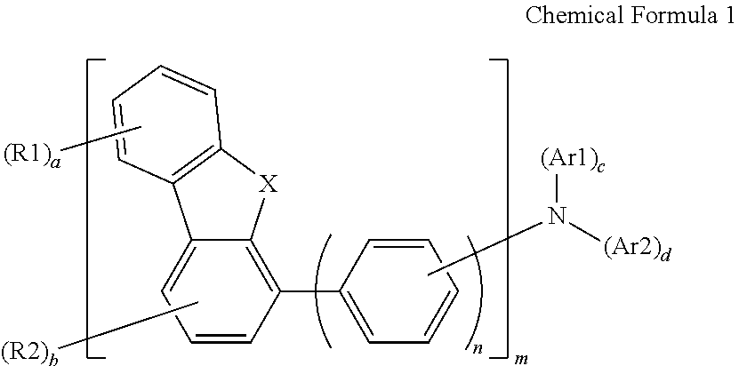

where, in the Chemical Formula 2,
-
- definitions of R1, R2, X, Ar1, Ar2, a, b, c and d, m are the same as in the Chemical Formula 1, respectively.

where, in each of the Chemical Formulas 3 to 5,
-
- definitions of R1, R2, X, Ar1, Ar2, a, b, c and d, m are the same as in the Chemical Formula 1, respectively.


where, in the Chemical Formula 1,
-
- X represents O or S,
- each of R1 and R2 independently represents a substituent selected from the group consisting of an aryl group having 6 to 30 carbon atoms, a heteroaryl group having 5 to 30 carbon atoms, an alkyl group having 1 to 15 carbon atoms, a halogen atom, and a deuterium atom,
- a is an integer from 0 to 4, when a is 2 or more, R1s are the same as or different from each other, or adjacent R1s may be bonded to each other to form a ring,
- b is an integer from 0 to 3, when b is 2 or more, R2s are the same as or different from each other, or adjacent R2s may be bonded to each other to form a ring,
- n is 0 or 1, n=0 representing a direct bond,
- m is an integer of 1 to 3,
- each of c and d is an integer of 0 or 1,
- m, c, and d are selected such that when m is 1, c+d=2, when m is 2, c+d=1, and when m is 3, c+d=0, and
- each of Ar1 and Ar2 independently represents one selected from the group consisting of a substituted or unsubstituted aryl group having 6 to 30 carbon atoms, an alkyl group having 1 to 30 carbon atoms, an alkenyl group having 2 to 30 carbon atoms, an alkynyl group having 2 to 20 carbon atoms, an alkoxyl group having 1 to 30 carbon atoms, and an aryloxy group having 6 to 30 carbon atoms.


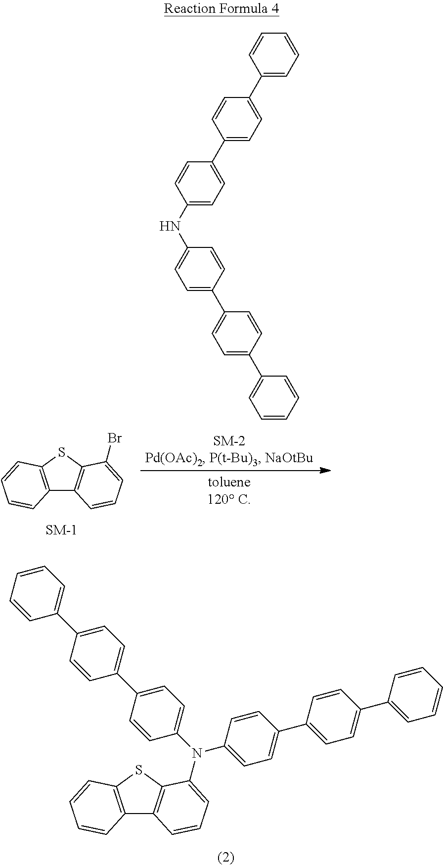


| TABLE 1 | ||||||||
| Drive | ||||||||
| Hole transport | voltage | mA/ | LT95 | |||||
| Examples | material | (V) | cm2 | Cd/A | lm/W | CIEx | CIEy | (hrs) |
| Comparative | NPB | 4.52 | 100% | 100% | 100% | 0.141 | 0.110 | 100% |
| Example 1 | ||||||||
| Example 1 | Compound 2 | 4.03 | 110% | 108% | 103% | 0.141 | 0.110 | 128% |
| Example 2 | Compound 3 | 4.05 | 111% | 108% | 105% | 0.141 | 0.111 | 125% |
| Example 3 | Compound 4 | 4.06 | 109% | 106% | 106% | 0.141 | 0.110 | 122% |
| Example 4 | Compound 14 | 4.08 | 109% | 107% | 106% | 0.140 | 0.111 | 134% |
| Example 5 | Compound 15 | 4.09 | 108% | 106% | 105% | 0.141 | 0.110 | 137% |
| Example 6 | Compound 18 | 4.16 | 114% | 110% | 111% | 0.139 | 0.110 | 138% |
| Example 7 | Compound 22 | 4.19 | 116% | 111% | 110% | 0.140 | 0.111 | 135% |
| Example 8 | Compound 24 | 4.17 | 114% | 112% | 109% | 0.141 | 0.110 | 137% |
| Example 9 | Compound 44 | 4.21 | 122% | 119% | 118% | 0.141 | 0.110 | 146% |
| Example 10 | Compound 45 | 4.20 | 120% | 116% | 115% | 0.141 | 0.111 | 142% |
| Example 11 | Compound 46 | 4.19 | 125% | 120% | 119% | 0.141 | 0.110 | 144% |
| Example 12 | Compound 57 | 4.38 | 128% | 122% | 120% | 0.141 | 0.111 | 152% |
| Example 13 | Compound 58 | 4.33 | 126% | 125% | 122% | 0.141 | 0.110 | 149% |
| Example 14 | Compound 59 | 4.30 | 122% | 121% | 120% | 0.141 | 0.111 | 151% |
Claims (13)


Priority Applications (1)
| Application Number | Priority Date | Filing Date | Title |
|---|---|---|---|
| US17/978,065 US11895911B2 (en) | 2018-12-21 | 2022-10-31 | Organic light emitting device |
Applications Claiming Priority (2)
| Application Number | Priority Date | Filing Date | Title |
|---|---|---|---|
| KR1020180167668A KR102169567B1 (en) | 2018-12-21 | 2018-12-21 | Organic Light Emitting Device |
| KR10-2018-0167668 | 2018-12-21 |
Related Child Applications (1)
| Application Number | Title | Priority Date | Filing Date |
|---|---|---|---|
| US17/978,065 Continuation US11895911B2 (en) | 2018-12-21 | 2022-10-31 | Organic light emitting device |
Publications (2)
| Publication Number | Publication Date |
|---|---|
| US20200203619A1 US20200203619A1 (en) | 2020-06-25 |
| US11515480B2 true US11515480B2 (en) | 2022-11-29 |
Family
ID=70969276
Family Applications (2)
| Application Number | Title | Priority Date | Filing Date |
|---|---|---|---|
| US16/721,777 Active 2040-09-27 US11515480B2 (en) | 2018-12-21 | 2019-12-19 | Organic light emitting device |
| US17/978,065 Active US11895911B2 (en) | 2018-12-21 | 2022-10-31 | Organic light emitting device |
Family Applications After (1)
| Application Number | Title | Priority Date | Filing Date |
|---|---|---|---|
| US17/978,065 Active US11895911B2 (en) | 2018-12-21 | 2022-10-31 | Organic light emitting device |
Country Status (4)
| Country | Link |
|---|---|
| US (2) | US11515480B2 (en) |
| KR (1) | KR102169567B1 (en) |
| CN (1) | CN111349073B (en) |
| DE (1) | DE102019134849A1 (en) |
Cited By (1)
| Publication number | Priority date | Publication date | Assignee | Title |
|---|---|---|---|---|
| US20220310740A1 (en) * | 2020-09-02 | 2022-09-29 | Shenzhen China Star Optoelectronics Semiconductor Display Technology Co., Ltd. | Oled display panel and manufacturing method thereof |
Families Citing this family (6)
| Publication number | Priority date | Publication date | Assignee | Title |
|---|---|---|---|---|
| US20220246857A1 (en) | 2019-05-31 | 2022-08-04 | Idemitsu Kosan Co.,Ltd. | Compound, material for organic electroluminescent elements, organic electroluminescent element, and electronic device |
| KR20200139398A (en) * | 2019-06-04 | 2020-12-14 | 주식회사 동진쎄미켐 | Compound for capping layer and organic electroluminescent divice including the same |
| WO2021193654A1 (en) * | 2020-03-25 | 2021-09-30 | 出光興産株式会社 | Compound, material for organic electroluminescent elements, organic electroluminescent element, and electronic device |
| KR20220162113A (en) * | 2020-03-31 | 2022-12-07 | 이데미쓰 고산 가부시키가이샤 | Chemical compounds, materials for organic electroluminescent devices, organic electroluminescent devices and electronic devices |
| US20230345817A1 (en) * | 2020-08-17 | 2023-10-26 | Hodogaya Chemical Co., Ltd. | Organic electroluminescent device |
| CN114057718A (en) * | 2022-01-17 | 2022-02-18 | 浙江华显光电科技有限公司 | Triphenylamine derivative, preparation, organic photoelectric device and display or lighting device |
Citations (16)
| Publication number | Priority date | Publication date | Assignee | Title |
|---|---|---|---|---|
| KR20140087883A (en) | 2012-12-31 | 2014-07-09 | 제일모직주식회사 | Organic optoelectronic device and display including the same |
| US20150034916A1 (en) * | 2013-07-30 | 2015-02-05 | Samsung Display Co., Ltd. | Organic light-emitting display apparatus and method of manufacturing the same |
| KR20150046069A (en) | 2012-08-30 | 2015-04-29 | 이데미쓰 고산 가부시키가이샤 | Aromatic amine derivative, and organic electroluminescent element using same |
| KR20150102734A (en) | 2014-02-28 | 2015-09-07 | 머티어리얼사이언스 주식회사 | Organic compounds for an organic electroluminescent device and an organic electroluminescent device comprising the same |
| US20160056387A1 (en) | 2014-08-21 | 2016-02-25 | Samsung Display Co., Ltd. | Organic light emitting diode and organic light emitting display device including the same |
| KR20160024625A (en) * | 2014-08-26 | 2016-03-07 | 삼성에스디아이 주식회사 | Organic optoelectric device and display device |
| US20160099420A1 (en) | 2014-10-06 | 2016-04-07 | Samsung Display Co., Ltd. | Organic electroluminescent material and organic electroluminescent device including the same |
| US20160133848A1 (en) | 2014-11-12 | 2016-05-12 | E-Ray Optoelectronics Techonology Co., Ltd. | Heterocyclic compounds and organic electroluminescent devices using the same |
| CN106232768A (en) | 2014-05-30 | 2016-12-14 | 三星Sdi株式会社 | Organic photovoltaic component and display element |
| KR20170127353A (en) | 2016-05-11 | 2017-11-21 | 에스케이케미칼주식회사 | Compound for organic electroluminescent device and organic electroluminescent device comprising the same |
| KR20170134163A (en) | 2016-05-27 | 2017-12-06 | 주식회사 엘지화학 | Organic light emitting device |
| KR20180078177A (en) | 2016-12-29 | 2018-07-09 | 머티어리얼사이언스 주식회사 | Organic compound and organic electroluminescent device comprising the same |
| CN108369996A (en) | 2015-12-17 | 2018-08-03 | 株式会社半导体能源研究所 | Light-emitting component, light-emitting device, electronic equipment, lighting device, lighting system and guiding system |
| CN108689913A (en) | 2017-04-05 | 2018-10-23 | 东进世美肯株式会社 | Compounds and organic luminescent device comprising it |
| CN111217778A (en) | 2018-11-27 | 2020-06-02 | 东进世美肯株式会社 | Organic compound for capping layer and organic light emitting device including the same |
| CN111247652A (en) | 2018-02-23 | 2020-06-05 | 株式会社Lg化学 | Organic light emitting device |
Family Cites Families (2)
| Publication number | Priority date | Publication date | Assignee | Title |
|---|---|---|---|---|
| KR100786292B1 (en) * | 2005-07-15 | 2007-12-18 | 삼성에스디아이 주식회사 | organic electroluminescence display device |
| WO2017196081A1 (en) | 2016-05-11 | 2017-11-16 | Sk Chemicals Co., Ltd. | Compound for organic electroluminescent device and organic electroluminescent device comprising the same |
-
2018
- 2018-12-21 KR KR1020180167668A patent/KR102169567B1/en active IP Right Grant
-
2019
- 2019-12-16 CN CN201911294317.XA patent/CN111349073B/en active Active
- 2019-12-18 DE DE102019134849.8A patent/DE102019134849A1/en active Pending
- 2019-12-19 US US16/721,777 patent/US11515480B2/en active Active
-
2022
- 2022-10-31 US US17/978,065 patent/US11895911B2/en active Active
Patent Citations (18)
| Publication number | Priority date | Publication date | Assignee | Title |
|---|---|---|---|---|
| KR20150046069A (en) | 2012-08-30 | 2015-04-29 | 이데미쓰 고산 가부시키가이샤 | Aromatic amine derivative, and organic electroluminescent element using same |
| CN104662010A (en) | 2012-08-30 | 2015-05-27 | 出光兴产株式会社 | Aromatic amine derivative and organic electroluminescent element using same |
| KR20140087883A (en) | 2012-12-31 | 2014-07-09 | 제일모직주식회사 | Organic optoelectronic device and display including the same |
| US20150034916A1 (en) * | 2013-07-30 | 2015-02-05 | Samsung Display Co., Ltd. | Organic light-emitting display apparatus and method of manufacturing the same |
| KR20150102734A (en) | 2014-02-28 | 2015-09-07 | 머티어리얼사이언스 주식회사 | Organic compounds for an organic electroluminescent device and an organic electroluminescent device comprising the same |
| CN106232768A (en) | 2014-05-30 | 2016-12-14 | 三星Sdi株式会社 | Organic photovoltaic component and display element |
| US20160056387A1 (en) | 2014-08-21 | 2016-02-25 | Samsung Display Co., Ltd. | Organic light emitting diode and organic light emitting display device including the same |
| CN106661445A (en) | 2014-08-26 | 2017-05-10 | 三星Sdi株式会社 | Organic optoelectronic element and display device |
| KR20160024625A (en) * | 2014-08-26 | 2016-03-07 | 삼성에스디아이 주식회사 | Organic optoelectric device and display device |
| US20160099420A1 (en) | 2014-10-06 | 2016-04-07 | Samsung Display Co., Ltd. | Organic electroluminescent material and organic electroluminescent device including the same |
| US20160133848A1 (en) | 2014-11-12 | 2016-05-12 | E-Ray Optoelectronics Techonology Co., Ltd. | Heterocyclic compounds and organic electroluminescent devices using the same |
| CN108369996A (en) | 2015-12-17 | 2018-08-03 | 株式会社半导体能源研究所 | Light-emitting component, light-emitting device, electronic equipment, lighting device, lighting system and guiding system |
| KR20170127353A (en) | 2016-05-11 | 2017-11-21 | 에스케이케미칼주식회사 | Compound for organic electroluminescent device and organic electroluminescent device comprising the same |
| KR20170134163A (en) | 2016-05-27 | 2017-12-06 | 주식회사 엘지화학 | Organic light emitting device |
| KR20180078177A (en) | 2016-12-29 | 2018-07-09 | 머티어리얼사이언스 주식회사 | Organic compound and organic electroluminescent device comprising the same |
| CN108689913A (en) | 2017-04-05 | 2018-10-23 | 东进世美肯株式会社 | Compounds and organic luminescent device comprising it |
| CN111247652A (en) | 2018-02-23 | 2020-06-05 | 株式会社Lg化学 | Organic light emitting device |
| CN111217778A (en) | 2018-11-27 | 2020-06-02 | 东进世美肯株式会社 | Organic compound for capping layer and organic light emitting device including the same |
Cited By (1)
| Publication number | Priority date | Publication date | Assignee | Title |
|---|---|---|---|---|
| US20220310740A1 (en) * | 2020-09-02 | 2022-09-29 | Shenzhen China Star Optoelectronics Semiconductor Display Technology Co., Ltd. | Oled display panel and manufacturing method thereof |
Also Published As
| Publication number | Publication date |
|---|---|
| CN111349073B (en) | 2023-08-01 |
| US20200203619A1 (en) | 2020-06-25 |
| US11895911B2 (en) | 2024-02-06 |
| KR20200078089A (en) | 2020-07-01 |
| KR102169567B1 (en) | 2020-10-23 |
| CN111349073A (en) | 2020-06-30 |
| US20230172060A1 (en) | 2023-06-01 |
| DE102019134849A1 (en) | 2020-06-25 |
Similar Documents
| Publication | Publication Date | Title |
|---|---|---|
| US11515480B2 (en) | Organic light emitting device | |
| US11342505B2 (en) | Organic compounds and organic electroluminescent device including the same | |
| US20200335705A1 (en) | Organic electroluminescent device | |
| US10014479B2 (en) | Organic light-emitting diode with high efficiency and long lifetime | |
| US11844270B2 (en) | Compound and organic light emitting device including the same | |
| US11302875B2 (en) | Organic electroluminescence device | |
| US11332474B2 (en) | Compound and organic light-emission device | |
| US11744145B2 (en) | Organic compound and organic electroluminescent device comprising the same | |
| US11696497B2 (en) | Organic light emitting device | |
| KR20170065733A (en) | Organic light emitting device and display device having the same | |
| US11545630B2 (en) | Compound and organic electroluminescent device comprising the same | |
| US20220209140A1 (en) | Organic metal compound, organic light emitting diode and organic light emitting device having the compound | |
| US9608211B2 (en) | Heterocyclic compound and organic light-emitting diode including the same | |
| US9634257B2 (en) | Heterocyclic compound and organic light-emitting device including the same | |
| US20140209871A1 (en) | Novel heterocyclic compound and organic light-emitting device including the same | |
| US20220246864A1 (en) | Novel organic compounds and organic electroluminescent device including the same | |
| US20220194883A1 (en) | Organic compound, and organic light emitting diode and organic light emitting device including the same | |
| US9755153B2 (en) | Organic compound and organic light emitting diode device including the same | |
| CN111349063B (en) | Organic light emitting device | |
| US20230203075A1 (en) | Organometallic compound and organic light-emitting diode including the same | |
| US20230203074A1 (en) | Organometallic compound and organic light-emitting diode including the same | |
| US20230209989A1 (en) | Organometallic compound and organic light-emitting diode including the same | |
| US20230200208A1 (en) | Organometallic compound and organic light-emitting diode including the same | |
| US20230209988A1 (en) | Organic light emitting diode and organic light emitting display device having the same | |
| US20230200209A1 (en) | Organometallic compound and organic light-emitting diode including the same |
Legal Events
| Date | Code | Title | Description |
|---|---|---|---|
| FEPP | Fee payment procedure |
Free format text: ENTITY STATUS SET TO UNDISCOUNTED (ORIGINAL EVENT CODE: BIG.); ENTITY STATUS OF PATENT OWNER: LARGE ENTITY |
|
| AS | Assignment |
Owner name: LG DISPLAY CO., LTD., KOREA, REPUBLIC OF Free format text: ASSIGNMENT OF ASSIGNORS INTEREST;ASSIGNORS:PARK, HEEJUN;YOO, SEONKEUN;JANG, SOYOUNG;AND OTHERS;SIGNING DATES FROM 20191113 TO 20191212;REEL/FRAME:051389/0985 |
|
| STPP | Information on status: patent application and granting procedure in general |
Free format text: DOCKETED NEW CASE - READY FOR EXAMINATION |
|
| STPP | Information on status: patent application and granting procedure in general |
Free format text: NON FINAL ACTION MAILED |
|
| STPP | Information on status: patent application and granting procedure in general |
Free format text: RESPONSE TO NON-FINAL OFFICE ACTION ENTERED AND FORWARDED TO EXAMINER |
|
| STPP | Information on status: patent application and granting procedure in general |
Free format text: NOTICE OF ALLOWANCE MAILED -- APPLICATION RECEIVED IN OFFICE OF PUBLICATIONS |
|
| STPP | Information on status: patent application and granting procedure in general |
Free format text: NOTICE OF ALLOWANCE MAILED -- APPLICATION RECEIVED IN OFFICE OF PUBLICATIONS |
|
| STPP | Information on status: patent application and granting procedure in general |
Free format text: PUBLICATIONS -- ISSUE FEE PAYMENT VERIFIED |
|
| STCF | Information on status: patent grant |
Free format text: PATENTED CASE |