US11512038B2 - Tetraphenylene triarylamine compounds - Google Patents
Tetraphenylene triarylamine compounds Download PDFInfo
- Publication number
- US11512038B2 US11512038B2 US16/223,135 US201816223135A US11512038B2 US 11512038 B2 US11512038 B2 US 11512038B2 US 201816223135 A US201816223135 A US 201816223135A US 11512038 B2 US11512038 B2 US 11512038B2
- Authority
- US
- United States
- Prior art keywords
- group
- hole transporting
- carbon atoms
- substituted
- transporting compound
- Prior art date
- Legal status (The legal status is an assumption and is not a legal conclusion. Google has not performed a legal analysis and makes no representation as to the accuracy of the status listed.)
- Active, expires
Links
- 0 *c1ccccc1-c1ccccc1*.Cc1ccccc1-c1ccccc1C.c1ccc2c(c1)CCc1ccccc1-2 Chemical compound *c1ccccc1-c1ccccc1*.Cc1ccccc1-c1ccccc1C.c1ccc2c(c1)CCc1ccccc1-2 0.000 description 5
- COYWQBPPDLTSMN-ATTBDTPUSA-N c1ccc(C2(c3ccccc3)c3ccccc3-c3c(N(c4ccc5c(c4)-c4ccccc4-c4ccccc4-c4ccccc4-5)c4ccc5c(c4)oc4ccccc45)cccc32)cc1.c1ccc(C2(c3ccccc3)c3ccccc3-c3c(N(c4ccc5c(c4)-c4ccccc4-c4ccccc4-c4ccccc4-5)c4ccc5c(c4)sc4ccccc45)cccc32)cc1.c1ccc(C2(c3ccccc3)c3ccccc3-c3c(N(c4ccc5c(c4)-c4ccccc4-c4ccccc4-c4ccccc4-5)c4cccc5c4sc4ccccc45)cccc32)cc1 Chemical compound c1ccc(C2(c3ccccc3)c3ccccc3-c3c(N(c4ccc5c(c4)-c4ccccc4-c4ccccc4-c4ccccc4-5)c4ccc5c(c4)oc4ccccc45)cccc32)cc1.c1ccc(C2(c3ccccc3)c3ccccc3-c3c(N(c4ccc5c(c4)-c4ccccc4-c4ccccc4-c4ccccc4-5)c4ccc5c(c4)sc4ccccc45)cccc32)cc1.c1ccc(C2(c3ccccc3)c3ccccc3-c3c(N(c4ccc5c(c4)-c4ccccc4-c4ccccc4-c4ccccc4-5)c4cccc5c4sc4ccccc45)cccc32)cc1 COYWQBPPDLTSMN-ATTBDTPUSA-N 0.000 description 3
- OCEJINBQSVLGRG-UHFFFAOYSA-N CC.CC.CC.CC.CC.CC.CC.CC.CC.CC.CC.CC.CC.CC.CC.CC.CC.CC.CC.CC.CC.CC.CC.CC.CC.CC.CC.CC.CC.CC.CC.CC.CC.CC.CC.CC.CC.CC.CC.CC.CC.CC.CC.CC.CC.CC.CC.CC.CC.CC1(C)c2ccccc2-c2ccccc21.CC1(C)c2ccccc2-c2ccccc21.Cc1ccccc1.c1cc(-c2ccncc2)ccn1.c1ccc(-c2ccccc2)cc1.c1ccc(-c2ccccc2)cc1.c1ccc(-c2ccccn2)nc1.c1ccc(-n2c3ccccc3c3ccccc32)cc1.c1ccc(-n2c3ccccc3c3ccccc32)cc1.c1ccc(C2(c3ccccc3)c3ccccc3-c3ccccc32)cc1.c1ccc(C2(c3ccccc3)c3ccccc3-c3ccccc32)cc1.c1ccc2c(c1)-c1ccccc1C21c2ccccc2-c2ccccc21.c1ccc2c(c1)-c1ccccc1C21c2ccccc2-c2ccccc21.c1ccc2c(c1)c1ccccc1c1ccccc21.c1ccc2c(c1)oc1ccccc12.c1ccc2c(c1)oc1ccccc12.c1ccc2c(c1)sc1ccccc12.c1ccc2c(c1)sc1ccccc12.c1ccc2ccccc2c1.c1ccc2ccccc2c1.c1ccncc1.c1cncc(-c2cccnc2)c1.c1cnccn1.c1cncnc1.c1ncncn1 Chemical compound CC.CC.CC.CC.CC.CC.CC.CC.CC.CC.CC.CC.CC.CC.CC.CC.CC.CC.CC.CC.CC.CC.CC.CC.CC.CC.CC.CC.CC.CC.CC.CC.CC.CC.CC.CC.CC.CC.CC.CC.CC.CC.CC.CC.CC.CC.CC.CC.CC.CC1(C)c2ccccc2-c2ccccc21.CC1(C)c2ccccc2-c2ccccc21.Cc1ccccc1.c1cc(-c2ccncc2)ccn1.c1ccc(-c2ccccc2)cc1.c1ccc(-c2ccccc2)cc1.c1ccc(-c2ccccn2)nc1.c1ccc(-n2c3ccccc3c3ccccc32)cc1.c1ccc(-n2c3ccccc3c3ccccc32)cc1.c1ccc(C2(c3ccccc3)c3ccccc3-c3ccccc32)cc1.c1ccc(C2(c3ccccc3)c3ccccc3-c3ccccc32)cc1.c1ccc2c(c1)-c1ccccc1C21c2ccccc2-c2ccccc21.c1ccc2c(c1)-c1ccccc1C21c2ccccc2-c2ccccc21.c1ccc2c(c1)c1ccccc1c1ccccc21.c1ccc2c(c1)oc1ccccc12.c1ccc2c(c1)oc1ccccc12.c1ccc2c(c1)sc1ccccc12.c1ccc2c(c1)sc1ccccc12.c1ccc2ccccc2c1.c1ccc2ccccc2c1.c1ccncc1.c1cncc(-c2cccnc2)c1.c1cnccn1.c1cncnc1.c1ncncn1 OCEJINBQSVLGRG-UHFFFAOYSA-N 0.000 description 2
- JEZZTYLRFFFKJZ-OHDWUNISSA-N c1ccc(-c2ccc(-c3ccc(N(c4ccc(-c5cccc6c5oc5ccccc56)cc4)c4ccc5c(c4)-c4ccccc4-c4ccccc4-c4ccccc4-5)cc3)cc2)cc1.c1ccc(-c2ccc(N(c3ccc(-c4cccc5c4oc4ccccc45)cc3)c3ccc4c(c3)-c3ccccc3-c3ccccc3-c3ccccc3-4)c(-c3ccccc3)c2)cc1.c1ccc(-c2ccc(N(c3ccc4c(c3)-c3ccccc3-c3ccccc3-c3ccccc3-4)c3ccc4sc5ccccc5c4c3)cc2)cc1 Chemical compound c1ccc(-c2ccc(-c3ccc(N(c4ccc(-c5cccc6c5oc5ccccc56)cc4)c4ccc5c(c4)-c4ccccc4-c4ccccc4-c4ccccc4-5)cc3)cc2)cc1.c1ccc(-c2ccc(N(c3ccc(-c4cccc5c4oc4ccccc45)cc3)c3ccc4c(c3)-c3ccccc3-c3ccccc3-c3ccccc3-4)c(-c3ccccc3)c2)cc1.c1ccc(-c2ccc(N(c3ccc4c(c3)-c3ccccc3-c3ccccc3-c3ccccc3-4)c3ccc4sc5ccccc5c4c3)cc2)cc1 JEZZTYLRFFFKJZ-OHDWUNISSA-N 0.000 description 2
- YLTXGYCAWSCNDR-SMHISTQOSA-N c1ccc(-c2ccc(-c3ccc(N(c4ccc5c(c4)-c4ccccc4-c4ccccc4-c4ccccc4-5)c4ccc5c(c4)-c4ccccc4C5(c4ccccc4)c4ccccc4)cc3)cc2)cc1.c1ccc(-c2ccc(N(c3ccc4c(c3)-c3ccccc3-c3ccccc3-c3ccccc3-4)c3ccc4c(c3)-c3ccccc3C4(c3ccccc3)c3ccccc3)cc2)cc1.c1ccc(-c2ccccc2N(c2ccc3c(c2)-c2ccccc2-c2ccccc2-c2ccccc2-3)c2ccc3c(c2)-c2ccccc2C3(c2ccccc2)c2ccccc2)cc1 Chemical compound c1ccc(-c2ccc(-c3ccc(N(c4ccc5c(c4)-c4ccccc4-c4ccccc4-c4ccccc4-5)c4ccc5c(c4)-c4ccccc4C5(c4ccccc4)c4ccccc4)cc3)cc2)cc1.c1ccc(-c2ccc(N(c3ccc4c(c3)-c3ccccc3-c3ccccc3-c3ccccc3-4)c3ccc4c(c3)-c3ccccc3C4(c3ccccc3)c3ccccc3)cc2)cc1.c1ccc(-c2ccccc2N(c2ccc3c(c2)-c2ccccc2-c2ccccc2-c2ccccc2-3)c2ccc3c(c2)-c2ccccc2C3(c2ccccc2)c2ccccc2)cc1 YLTXGYCAWSCNDR-SMHISTQOSA-N 0.000 description 2
- RKRXQXURLASPKG-KZTFQTCESA-N c1ccc(-c2ccc(-c3ccc(N(c4ccc5c(c4)-c4ccccc4-c4ccccc4-c4ccccc4-5)c4ccc5c(c4)oc4ccccc45)cc3)cc2)cc1.c1ccc(-c2ccc(N(c3ccc4c(c3)-c3ccccc3-c3ccccc3-c3ccccc3-4)c3ccc4c(c3)oc3ccccc34)c(-c3ccccc3)c2)cc1.c1ccc(-c2ccc(N(c3ccc4c(c3)-c3ccccc3-c3ccccc3-c3ccccc3-4)c3ccc4c(c3)oc3ccccc34)cc2)cc1.c1ccc(-c2ccc(N(c3ccc4c(c3)-c3ccccc3-c3ccccc3-c3ccccc3-4)c3cccc4c3oc3ccccc34)c(-c3ccccc3)c2)cc1 Chemical compound c1ccc(-c2ccc(-c3ccc(N(c4ccc5c(c4)-c4ccccc4-c4ccccc4-c4ccccc4-5)c4ccc5c(c4)oc4ccccc45)cc3)cc2)cc1.c1ccc(-c2ccc(N(c3ccc4c(c3)-c3ccccc3-c3ccccc3-c3ccccc3-4)c3ccc4c(c3)oc3ccccc34)c(-c3ccccc3)c2)cc1.c1ccc(-c2ccc(N(c3ccc4c(c3)-c3ccccc3-c3ccccc3-c3ccccc3-4)c3ccc4c(c3)oc3ccccc34)cc2)cc1.c1ccc(-c2ccc(N(c3ccc4c(c3)-c3ccccc3-c3ccccc3-c3ccccc3-4)c3cccc4c3oc3ccccc34)c(-c3ccccc3)c2)cc1 RKRXQXURLASPKG-KZTFQTCESA-N 0.000 description 2
- VFZCPORYZBTRBU-KZTFQTCESA-N c1ccc(-c2ccc(-c3ccc(N(c4ccc5c(c4)-c4ccccc4-c4ccccc4-c4ccccc4-5)c4ccc5c(c4)sc4ccccc45)cc3)cc2)cc1.c1ccc(-c2ccc(N(c3ccc4c(c3)-c3ccccc3-c3ccccc3-c3ccccc3-4)c3ccc4c(c3)sc3ccccc34)c(-c3ccccc3)c2)cc1.c1ccc(-c2ccc(N(c3ccc4c(c3)-c3ccccc3-c3ccccc3-c3ccccc3-4)c3ccc4c(c3)sc3ccccc34)cc2)cc1.c1ccc(-c2ccc(N(c3ccc4c(c3)-c3ccccc3-c3ccccc3-c3ccccc3-4)c3cccc4c3sc3ccccc34)c(-c3ccccc3)c2)cc1 Chemical compound c1ccc(-c2ccc(-c3ccc(N(c4ccc5c(c4)-c4ccccc4-c4ccccc4-c4ccccc4-5)c4ccc5c(c4)sc4ccccc45)cc3)cc2)cc1.c1ccc(-c2ccc(N(c3ccc4c(c3)-c3ccccc3-c3ccccc3-c3ccccc3-4)c3ccc4c(c3)sc3ccccc34)c(-c3ccccc3)c2)cc1.c1ccc(-c2ccc(N(c3ccc4c(c3)-c3ccccc3-c3ccccc3-c3ccccc3-4)c3ccc4c(c3)sc3ccccc34)cc2)cc1.c1ccc(-c2ccc(N(c3ccc4c(c3)-c3ccccc3-c3ccccc3-c3ccccc3-4)c3cccc4c3sc3ccccc34)c(-c3ccccc3)c2)cc1 VFZCPORYZBTRBU-KZTFQTCESA-N 0.000 description 2
- SQELMBVWRZPLCX-LOLHKZHTSA-N c1ccc(-c2ccc(-c3ccc(N(c4ccc5c(c4)-c4ccccc4-c4ccccc4-c4ccccc4-5)c4ccc5oc6ccccc6c5c4)cc3)cc2)cc1.c1ccc(-c2ccc(-c3ccc(N(c4ccc5c(c4)-c4ccccc4-c4ccccc4-c4ccccc4-5)c4cccc5c4oc4ccccc45)cc3)cc2)cc1.c1ccc(-c2ccc(N(c3ccc4c(c3)-c3ccccc3-c3ccccc3-c3ccccc3-4)c3ccc4oc5ccccc5c4c3)c(-c3ccccc3)c2)cc1.c1ccc(-c2ccc(N(c3ccc4c(c3)-c3ccccc3-c3ccccc3-c3ccccc3-4)c3cccc4c3oc3ccccc34)cc2)cc1 Chemical compound c1ccc(-c2ccc(-c3ccc(N(c4ccc5c(c4)-c4ccccc4-c4ccccc4-c4ccccc4-5)c4ccc5oc6ccccc6c5c4)cc3)cc2)cc1.c1ccc(-c2ccc(-c3ccc(N(c4ccc5c(c4)-c4ccccc4-c4ccccc4-c4ccccc4-5)c4cccc5c4oc4ccccc45)cc3)cc2)cc1.c1ccc(-c2ccc(N(c3ccc4c(c3)-c3ccccc3-c3ccccc3-c3ccccc3-4)c3ccc4oc5ccccc5c4c3)c(-c3ccccc3)c2)cc1.c1ccc(-c2ccc(N(c3ccc4c(c3)-c3ccccc3-c3ccccc3-c3ccccc3-4)c3cccc4c3oc3ccccc34)cc2)cc1 SQELMBVWRZPLCX-LOLHKZHTSA-N 0.000 description 2
- HEYUXVQVTSPVBG-LOLHKZHTSA-N c1ccc(-c2ccc(-c3ccc(N(c4ccc5c(c4)-c4ccccc4-c4ccccc4-c4ccccc4-5)c4ccc5sc6ccccc6c5c4)cc3)cc2)cc1.c1ccc(-c2ccc(-c3ccc(N(c4ccc5c(c4)-c4ccccc4-c4ccccc4-c4ccccc4-5)c4cccc5c4sc4ccccc45)cc3)cc2)cc1.c1ccc(-c2ccc(N(c3ccc4c(c3)-c3ccccc3-c3ccccc3-c3ccccc3-4)c3ccc4sc5ccccc5c4c3)c(-c3ccccc3)c2)cc1.c1ccc(-c2ccc(N(c3ccc4c(c3)-c3ccccc3-c3ccccc3-c3ccccc3-4)c3cccc4c3sc3ccccc34)cc2)cc1 Chemical compound c1ccc(-c2ccc(-c3ccc(N(c4ccc5c(c4)-c4ccccc4-c4ccccc4-c4ccccc4-5)c4ccc5sc6ccccc6c5c4)cc3)cc2)cc1.c1ccc(-c2ccc(-c3ccc(N(c4ccc5c(c4)-c4ccccc4-c4ccccc4-c4ccccc4-5)c4cccc5c4sc4ccccc45)cc3)cc2)cc1.c1ccc(-c2ccc(N(c3ccc4c(c3)-c3ccccc3-c3ccccc3-c3ccccc3-4)c3ccc4sc5ccccc5c4c3)c(-c3ccccc3)c2)cc1.c1ccc(-c2ccc(N(c3ccc4c(c3)-c3ccccc3-c3ccccc3-c3ccccc3-4)c3cccc4c3sc3ccccc34)cc2)cc1 HEYUXVQVTSPVBG-LOLHKZHTSA-N 0.000 description 2
- BSFFJCZIMRSOIH-QJVDKNGZSA-N c1ccc(-c2ccc(-c3ccc(N(c4ccc5c(c4)-c4ccccc4-c4ccccc4-c4ccccc4-5)c4cccc5c4-c4ccccc4C5(c4ccccc4)c4ccccc4)cc3)cc2)cc1.c1ccc(-c2ccc(N(c3ccc4c(c3)-c3ccccc3-c3ccccc3-c3ccccc3-4)c3ccc4c(c3)-c3ccccc3C4(c3ccccc3)c3ccccc3)c(-c3ccccc3)c2)cc1.c1ccc(-c2ccc(N(c3ccc4c(c3)-c3ccccc3-c3ccccc3-c3ccccc3-4)c3cccc4c3-c3ccccc3C4(c3ccccc3)c3ccccc3)cc2)cc1 Chemical compound c1ccc(-c2ccc(-c3ccc(N(c4ccc5c(c4)-c4ccccc4-c4ccccc4-c4ccccc4-5)c4cccc5c4-c4ccccc4C5(c4ccccc4)c4ccccc4)cc3)cc2)cc1.c1ccc(-c2ccc(N(c3ccc4c(c3)-c3ccccc3-c3ccccc3-c3ccccc3-4)c3ccc4c(c3)-c3ccccc3C4(c3ccccc3)c3ccccc3)c(-c3ccccc3)c2)cc1.c1ccc(-c2ccc(N(c3ccc4c(c3)-c3ccccc3-c3ccccc3-c3ccccc3-4)c3cccc4c3-c3ccccc3C4(c3ccccc3)c3ccccc3)cc2)cc1 BSFFJCZIMRSOIH-QJVDKNGZSA-N 0.000 description 2
- IIRKUEPBWKGIIO-ZCQAKGIWSA-N c1ccc(-c2ccc(-c3ccc(N(c4ccc5c(c4)-c4ccccc4-c4ccccc4-c4ccccc4-5)c4cccc5oc6ccccc6c45)cc3)cc2)cc1.c1ccc(-c2ccc(N(c3ccc(-c4cccc5c4oc4ccccc45)cc3)c3ccc4c(c3)-c3ccccc3-c3ccccc3-c3ccccc3-4)cc2)cc1.c1ccc(-c2ccc(N(c3ccc4c(c3)-c3ccccc3-c3ccccc3-c3ccccc3-4)c3cccc4oc5ccccc5c34)c(-c3ccccc3)c2)cc1.c1ccc(-c2ccc(N(c3ccc4c(c3)-c3ccccc3-c3ccccc3-c3ccccc3-4)c3cccc4oc5ccccc5c34)cc2)cc1 Chemical compound c1ccc(-c2ccc(-c3ccc(N(c4ccc5c(c4)-c4ccccc4-c4ccccc4-c4ccccc4-5)c4cccc5oc6ccccc6c45)cc3)cc2)cc1.c1ccc(-c2ccc(N(c3ccc(-c4cccc5c4oc4ccccc45)cc3)c3ccc4c(c3)-c3ccccc3-c3ccccc3-c3ccccc3-4)cc2)cc1.c1ccc(-c2ccc(N(c3ccc4c(c3)-c3ccccc3-c3ccccc3-c3ccccc3-4)c3cccc4oc5ccccc5c34)c(-c3ccccc3)c2)cc1.c1ccc(-c2ccc(N(c3ccc4c(c3)-c3ccccc3-c3ccccc3-c3ccccc3-4)c3cccc4oc5ccccc5c34)cc2)cc1 IIRKUEPBWKGIIO-ZCQAKGIWSA-N 0.000 description 2
- XALOEWYJKCUNQS-ZCQAKGIWSA-N c1ccc(-c2ccc(-c3ccc(N(c4ccc5c(c4)-c4ccccc4-c4ccccc4-c4ccccc4-5)c4cccc5sc6ccccc6c45)cc3)cc2)cc1.c1ccc(-c2ccc(N(c3ccc(-c4cccc5c4sc4ccccc45)cc3)c3ccc4c(c3)-c3ccccc3-c3ccccc3-c3ccccc3-4)cc2)cc1.c1ccc(-c2ccc(N(c3ccc4c(c3)-c3ccccc3-c3ccccc3-c3ccccc3-4)c3cccc4sc5ccccc5c34)c(-c3ccccc3)c2)cc1.c1ccc(-c2ccc(N(c3ccc4c(c3)-c3ccccc3-c3ccccc3-c3ccccc3-4)c3cccc4sc5ccccc5c34)cc2)cc1 Chemical compound c1ccc(-c2ccc(-c3ccc(N(c4ccc5c(c4)-c4ccccc4-c4ccccc4-c4ccccc4-5)c4cccc5sc6ccccc6c45)cc3)cc2)cc1.c1ccc(-c2ccc(N(c3ccc(-c4cccc5c4sc4ccccc45)cc3)c3ccc4c(c3)-c3ccccc3-c3ccccc3-c3ccccc3-4)cc2)cc1.c1ccc(-c2ccc(N(c3ccc4c(c3)-c3ccccc3-c3ccccc3-c3ccccc3-4)c3cccc4sc5ccccc5c34)c(-c3ccccc3)c2)cc1.c1ccc(-c2ccc(N(c3ccc4c(c3)-c3ccccc3-c3ccccc3-c3ccccc3-4)c3cccc4sc5ccccc5c34)cc2)cc1 XALOEWYJKCUNQS-ZCQAKGIWSA-N 0.000 description 2
- DQIZWGHNTDJOJY-RKVWBUOSSA-N c1ccc(C2(c3ccccc3)c3ccccc3-c3c(N(c4ccc(-c5cccc6c5oc5ccccc56)cc4)c4ccc5c(c4)-c4ccccc4-c4ccccc4-c4ccccc4-5)cccc32)cc1.c1ccc(C2(c3ccccc3)c3ccccc3-c3c(N(c4ccc5c(c4)-c4ccccc4-c4ccccc4-c4ccccc4-5)c4ccc5oc6ccccc6c5c4)cccc32)cc1.c1ccc(C2(c3ccccc3)c3ccccc3-c3c(N(c4ccc5c(c4)-c4ccccc4-c4ccccc4-c4ccccc4-5)c4ccc5sc6ccccc6c5c4)cccc32)cc1 Chemical compound c1ccc(C2(c3ccccc3)c3ccccc3-c3c(N(c4ccc(-c5cccc6c5oc5ccccc56)cc4)c4ccc5c(c4)-c4ccccc4-c4ccccc4-c4ccccc4-5)cccc32)cc1.c1ccc(C2(c3ccccc3)c3ccccc3-c3c(N(c4ccc5c(c4)-c4ccccc4-c4ccccc4-c4ccccc4-5)c4ccc5oc6ccccc6c5c4)cccc32)cc1.c1ccc(C2(c3ccccc3)c3ccccc3-c3c(N(c4ccc5c(c4)-c4ccccc4-c4ccccc4-c4ccccc4-5)c4ccc5sc6ccccc6c5c4)cccc32)cc1 DQIZWGHNTDJOJY-RKVWBUOSSA-N 0.000 description 2
- PJZWJIKHDMCQDU-JPNKYJKDSA-N Brc1ccc2c(c1)-c1ccccc1-c1ccccc1-c1ccccc1-2.CC1(C)c2ccccc2-c2ccc(Cc3ccc(-c4ccccc4)cc3)cc21.CC1(C)c2ccccc2-c2ccc(N(c3ccc(-c4ccccc4)cc3)c3ccc4c(c3)-c3ccccc3-c3ccccc3-c3ccccc3-4)cc21 Chemical compound Brc1ccc2c(c1)-c1ccccc1-c1ccccc1-c1ccccc1-2.CC1(C)c2ccccc2-c2ccc(Cc3ccc(-c4ccccc4)cc3)cc21.CC1(C)c2ccccc2-c2ccc(N(c3ccc(-c4ccccc4)cc3)c3ccc4c(c3)-c3ccccc3-c3ccccc3-c3ccccc3-4)cc21 PJZWJIKHDMCQDU-JPNKYJKDSA-N 0.000 description 1
- DMBCCQFDIIIWHD-LCKMOYPPSA-N Brc1ccc2c(c1)-c1ccccc1-c1ccccc1-c1ccccc1-2.CC1(C)c2ccccc2-c2ccc(N(c3ccc(-c4ccccc4)cc3)c3ccc(-c4ccc5c(c4)-c4ccccc4-c4ccccc4-c4ccccc4-5)cc3)cc21.CC1(C)c2ccccc2-c2ccc(N(c3ccc(B(O)O)cc3)c3ccc(-c4ccccc4)cc3)cc21 Chemical compound Brc1ccc2c(c1)-c1ccccc1-c1ccccc1-c1ccccc1-2.CC1(C)c2ccccc2-c2ccc(N(c3ccc(-c4ccccc4)cc3)c3ccc(-c4ccc5c(c4)-c4ccccc4-c4ccccc4-c4ccccc4-5)cc3)cc21.CC1(C)c2ccccc2-c2ccc(N(c3ccc(B(O)O)cc3)c3ccc(-c4ccccc4)cc3)cc21 DMBCCQFDIIIWHD-LCKMOYPPSA-N 0.000 description 1
- XDGPLNYMFIINOQ-KJPOKFFDSA-N Brc1ccc2c(c1)-c1ccccc1-c1ccccc1-c1ccccc1-2.c1ccc(-c2ccc(Cc3ccc(-c4ccccc4)cc3)cc2)cc1.c1ccc(-c2ccc(N(c3ccc(-c4ccccc4)cc3)c3ccc4c(c3)-c3ccccc3-c3ccccc3-c3ccccc3-4)cc2)cc1 Chemical compound Brc1ccc2c(c1)-c1ccccc1-c1ccccc1-c1ccccc1-2.c1ccc(-c2ccc(Cc3ccc(-c4ccccc4)cc3)cc2)cc1.c1ccc(-c2ccc(N(c3ccc(-c4ccccc4)cc3)c3ccc4c(c3)-c3ccccc3-c3ccccc3-c3ccccc3-4)cc2)cc1 XDGPLNYMFIINOQ-KJPOKFFDSA-N 0.000 description 1
- OAMSBRVSHPIFEN-ZHPUYSMLSA-N Brc1ccc2c(c1)-c1ccccc1-c1ccccc1-c1ccccc1-2.c1ccc(-c2ccc(N(c3ccc(-c4ccc5c(c4)c4ccccc4n5-c4ccccc4)cc3)c3ccc4c(c3)-c3ccccc3-c3ccccc3-c3ccccc3-4)cc2)cc1.c1ccc(-c2ccc(Nc3ccc(-c4ccc5c(c4)c4ccccc4n5-c4ccccc4)cc3)cc2)cc1 Chemical compound Brc1ccc2c(c1)-c1ccccc1-c1ccccc1-c1ccccc1-2.c1ccc(-c2ccc(N(c3ccc(-c4ccc5c(c4)c4ccccc4n5-c4ccccc4)cc3)c3ccc4c(c3)-c3ccccc3-c3ccccc3-c3ccccc3-4)cc2)cc1.c1ccc(-c2ccc(Nc3ccc(-c4ccc5c(c4)c4ccccc4n5-c4ccccc4)cc3)cc2)cc1 OAMSBRVSHPIFEN-ZHPUYSMLSA-N 0.000 description 1
- XPYAHGKCTXPHCR-ZOOQHNRQSA-N Brc1ccc2c(c1)-c1ccccc1-c1ccccc1-c1ccccc1-2.c1ccc2c(c1)-c1ccccc1-c1ccccc1-c1ccccc1-2 Chemical compound Brc1ccc2c(c1)-c1ccccc1-c1ccccc1-c1ccccc1-2.c1ccc2c(c1)-c1ccccc1-c1ccccc1-c1ccccc1-2 XPYAHGKCTXPHCR-ZOOQHNRQSA-N 0.000 description 1
- WVRQSTHRJXNDBO-UHFFFAOYSA-N CC.CC.CC.CC.CC.CC.CC.CC.CC.CC.CC.CC.CC.CC.CC.CC.CC.CC.CC.CC.CC.CC.CC.CC.CC.CC.CC.CC.CC.CC.CC.CC.CC.CC.CC.CC.CC.CC1(C)c2ccccc2-c2ccccc21.CC1(C)c2ccccc2-c2ccccc21.Cc1ccccc1.c1cc(-c2ccncc2)ccn1.c1ccc(-c2ccccc2)cc1.c1ccc(-c2ccccc2)cc1.c1ccc(-c2ccccn2)nc1.c1ccc(C2(c3ccccc3)c3ccccc3-c3ccccc32)cc1.c1ccc(C2(c3ccccc3)c3ccccc3-c3ccccc32)cc1.c1ccc2c(c1)-c1ccccc1C21c2ccccc2-c2ccccc21.c1ccc2c(c1)-c1ccccc1C21c2ccccc2-c2ccccc21.c1ccc2c(c1)c1ccccc1c1ccccc21.c1ccc2ccccc2c1.c1ccc2ccccc2c1.c1ccncc1.c1cncc(-c2cccnc2)c1.c1cnccn1.c1cncnc1.c1ncncn1 Chemical compound CC.CC.CC.CC.CC.CC.CC.CC.CC.CC.CC.CC.CC.CC.CC.CC.CC.CC.CC.CC.CC.CC.CC.CC.CC.CC.CC.CC.CC.CC.CC.CC.CC.CC.CC.CC.CC.CC1(C)c2ccccc2-c2ccccc21.CC1(C)c2ccccc2-c2ccccc21.Cc1ccccc1.c1cc(-c2ccncc2)ccn1.c1ccc(-c2ccccc2)cc1.c1ccc(-c2ccccc2)cc1.c1ccc(-c2ccccn2)nc1.c1ccc(C2(c3ccccc3)c3ccccc3-c3ccccc32)cc1.c1ccc(C2(c3ccccc3)c3ccccc3-c3ccccc32)cc1.c1ccc2c(c1)-c1ccccc1C21c2ccccc2-c2ccccc21.c1ccc2c(c1)-c1ccccc1C21c2ccccc2-c2ccccc21.c1ccc2c(c1)c1ccccc1c1ccccc21.c1ccc2ccccc2c1.c1ccc2ccccc2c1.c1ccncc1.c1cncc(-c2cccnc2)c1.c1cnccn1.c1cncnc1.c1ncncn1 WVRQSTHRJXNDBO-UHFFFAOYSA-N 0.000 description 1
- BDMPNNOKTICSNT-UHFFFAOYSA-N CC.CC.CC.CC.CC.CC.CC.CC.CC.CC.CC.CC.Cc1ccccc1.Cc1ccccc1.c1ccc2c(c1)-c1ccccc1C21c2ccccc2-c2c1ccc1ccccc21.c1ccc2c(c1)-c1ccccc1C21c2ccccc2-c2c1ccc1ccccc21.c1ccc2c(c1)c1ccccc1c1ccccc21.c1ccc2c(c1)c1ccccc1c1ccccc21.c1ccc2c(c1)oc1cccnc12.c1ccc2c(c1)oc1ccncc12.c1ccc2c(c1)oc1cnccc12.c1ccc2c(c1)oc1cnccc12.c1ccc2c(c1)oc1cncnc12.c1ccc2c(c1)oc1ncccc12.c1ccc2c(c1)oc1ncccc12.c1ccccc1 Chemical compound CC.CC.CC.CC.CC.CC.CC.CC.CC.CC.CC.CC.Cc1ccccc1.Cc1ccccc1.c1ccc2c(c1)-c1ccccc1C21c2ccccc2-c2c1ccc1ccccc21.c1ccc2c(c1)-c1ccccc1C21c2ccccc2-c2c1ccc1ccccc21.c1ccc2c(c1)c1ccccc1c1ccccc21.c1ccc2c(c1)c1ccccc1c1ccccc21.c1ccc2c(c1)oc1cccnc12.c1ccc2c(c1)oc1ccncc12.c1ccc2c(c1)oc1cnccc12.c1ccc2c(c1)oc1cnccc12.c1ccc2c(c1)oc1cncnc12.c1ccc2c(c1)oc1ncccc12.c1ccc2c(c1)oc1ncccc12.c1ccccc1 BDMPNNOKTICSNT-UHFFFAOYSA-N 0.000 description 1
- VDAHSCAPJDQPAC-UHFFFAOYSA-N CC.CC.CC.CC.CC.CC.CC.CC.CC.CC.CC.Cc1ccccc1.Cc1ccccc1.Cc1ccccc1.Cc1ccccc1.Cc1ccccc1.Cc1ccccc1.Cc1ccccc1.Cc1ccccc1.c1ccc(-c2ccccc2)cc1.c1ccc(-c2ccccc2)cc1.c1ccc(-c2ccccc2)cc1.c1ccc2c(c1)oc1ccccc12.c1ccc2c(c1)oc1ccccc12.c1ccc2c(c1)oc1ccccc12.c1ccc2c(c1)oc1ccccc12.c1ccc2ccccc2c1.c1ccc2ccccc2c1.c1ccc2ccccc2c1.c1ccccc1 Chemical compound CC.CC.CC.CC.CC.CC.CC.CC.CC.CC.CC.Cc1ccccc1.Cc1ccccc1.Cc1ccccc1.Cc1ccccc1.Cc1ccccc1.Cc1ccccc1.Cc1ccccc1.Cc1ccccc1.c1ccc(-c2ccccc2)cc1.c1ccc(-c2ccccc2)cc1.c1ccc(-c2ccccc2)cc1.c1ccc2c(c1)oc1ccccc12.c1ccc2c(c1)oc1ccccc12.c1ccc2c(c1)oc1ccccc12.c1ccc2c(c1)oc1ccccc12.c1ccc2ccccc2c1.c1ccc2ccccc2c1.c1ccc2ccccc2c1.c1ccccc1 VDAHSCAPJDQPAC-UHFFFAOYSA-N 0.000 description 1
- PGRYURCKEQHRGS-UHFFFAOYSA-N CC.CC.CC.CC.CC.CC.CC.CC.CC.CC.Cc1ccccc1.Cc1ccccc1.Cc1ccccc1.Cc1ccccc1.Cc1ccccc1.c1ccc2c(c1)oc1cccnc12.c1ccc2c(c1)oc1ccncc12.c1ccc2c(c1)sc1cccnc12.c1ccc2c(c1)sc1ccncc12.c1ccc2c(c1)sc1ccncc12.c1ccc2c(c1)sc1cnccc12.c1ccc2c(c1)sc1cnccc12.c1ccc2c(c1)sc1cncnc12.c1ccc2c(c1)sc1ncccc12.c1ccc2c(c1)sc1ncccc12 Chemical compound CC.CC.CC.CC.CC.CC.CC.CC.CC.CC.Cc1ccccc1.Cc1ccccc1.Cc1ccccc1.Cc1ccccc1.Cc1ccccc1.c1ccc2c(c1)oc1cccnc12.c1ccc2c(c1)oc1ccncc12.c1ccc2c(c1)sc1cccnc12.c1ccc2c(c1)sc1ccncc12.c1ccc2c(c1)sc1ccncc12.c1ccc2c(c1)sc1cnccc12.c1ccc2c(c1)sc1cnccc12.c1ccc2c(c1)sc1cncnc12.c1ccc2c(c1)sc1ncccc12.c1ccc2c(c1)sc1ncccc12 PGRYURCKEQHRGS-UHFFFAOYSA-N 0.000 description 1
- XBWGAGAWGVNUNF-UHFFFAOYSA-N CC.CC.CC.CC.CC.CC.CC.CC.CC.Cc1ccccc1.Cc1ccccc1.Cc1ccccc1.Cc1ccccc1.Cc1ccccc1.Cc1ccccc1.Cc1ccccc1.c1ccc(-n2c3ccccc3c3ccccc32)cc1.c1ccc(-n2c3ccccc3c3ccccc32)cc1.c1ccc(-n2c3ccccc3c3ccccc32)cc1.c1ccc(-n2c3ccccc3c3ccccc32)cc1.c1ccc(-n2c3ccccc3c3ccccc32)cc1.c1ccc2c(c1)sc1ccccc12.c1ccc2c(c1)sc1ccccc12.c1ccc2c(c1)sc1ccccc12.c1ccc2c(c1)sc1ccccc12 Chemical compound CC.CC.CC.CC.CC.CC.CC.CC.CC.Cc1ccccc1.Cc1ccccc1.Cc1ccccc1.Cc1ccccc1.Cc1ccccc1.Cc1ccccc1.Cc1ccccc1.c1ccc(-n2c3ccccc3c3ccccc32)cc1.c1ccc(-n2c3ccccc3c3ccccc32)cc1.c1ccc(-n2c3ccccc3c3ccccc32)cc1.c1ccc(-n2c3ccccc3c3ccccc32)cc1.c1ccc(-n2c3ccccc3c3ccccc32)cc1.c1ccc2c(c1)sc1ccccc12.c1ccc2c(c1)sc1ccccc12.c1ccc2c(c1)sc1ccccc12.c1ccc2c(c1)sc1ccccc12 XBWGAGAWGVNUNF-UHFFFAOYSA-N 0.000 description 1
- AHKQNKNUVCZSFZ-UHFFFAOYSA-N CC.CC.CC.CC.CC.CC.CC.CC1(C)c2ccccc2-c2c1ccc1ccccc21.c1ccc(C2(c3ccccc3)c3ccccc3-c3c2ccc2ccccc32)cc1.c1ccc(C2(c3ccccc3)c3ccccc3-c3c2ccc2ccccc32)cc1.c1ccc(C2(c3ccccc3)c3ccccc3-c3c2ccc2ccccc32)cc1.c1ccc2c(c1)-c1ccccc1C21c2ccccc2-c2c1ccc1ccccc21 Chemical compound CC.CC.CC.CC.CC.CC.CC.CC1(C)c2ccccc2-c2c1ccc1ccccc21.c1ccc(C2(c3ccccc3)c3ccccc3-c3c2ccc2ccccc32)cc1.c1ccc(C2(c3ccccc3)c3ccccc3-c3c2ccc2ccccc32)cc1.c1ccc(C2(c3ccccc3)c3ccccc3-c3c2ccc2ccccc32)cc1.c1ccc2c(c1)-c1ccccc1C21c2ccccc2-c2c1ccc1ccccc21 AHKQNKNUVCZSFZ-UHFFFAOYSA-N 0.000 description 1
- CEOBUASBDJHQRD-UHFFFAOYSA-N CC.CC.CC.CC.CC.CC.CC1(C)c2ccccc2-c2ccccc21.CC1(C)c2ccccc2-c2ccccc21.CC1(C)c2ccccc2-c2ccccc21.CC1(C)c2ccccc2-c2ccccc21.Cc1ccccc1.Cc1ccccc1.Cc1ccccc1.Cc1ccccc1.Cc1ccccc1.c1ccc(-n2c3ccccc3c3ccccc32)cc1.c1ccc(C2(c3ccccc3)c3ccccc3-c3ccccc32)cc1 Chemical compound CC.CC.CC.CC.CC.CC.CC1(C)c2ccccc2-c2ccccc21.CC1(C)c2ccccc2-c2ccccc21.CC1(C)c2ccccc2-c2ccccc21.CC1(C)c2ccccc2-c2ccccc21.Cc1ccccc1.Cc1ccccc1.Cc1ccccc1.Cc1ccccc1.Cc1ccccc1.c1ccc(-n2c3ccccc3c3ccccc32)cc1.c1ccc(C2(c3ccccc3)c3ccccc3-c3ccccc32)cc1 CEOBUASBDJHQRD-UHFFFAOYSA-N 0.000 description 1
- MPNHGFULJSOUJN-UHFFFAOYSA-N CC.CC.CC.CC.CC.CC.Cc1ccccc1.Cc1ccccc1.Cc1ccccc1.Cc1ccccc1.c1ccc(C2(c3ccccc3)c3ccccc3-c3ccccc32)cc1.c1ccc(C2(c3ccccc3)c3ccccc3-c3ccccc32)cc1.c1ccc(C2(c3ccccc3)c3ccccc3-c3ccccc32)cc1.c1ccc(C2(c3ccccc3)c3ccccc3-c3ccccc32)cc1.c1ccc(C2(c3ccccc3)c3ccccc3-c3ccccc32)cc1.c1ccccc1 Chemical compound CC.CC.CC.CC.CC.CC.Cc1ccccc1.Cc1ccccc1.Cc1ccccc1.Cc1ccccc1.c1ccc(C2(c3ccccc3)c3ccccc3-c3ccccc32)cc1.c1ccc(C2(c3ccccc3)c3ccccc3-c3ccccc32)cc1.c1ccc(C2(c3ccccc3)c3ccccc3-c3ccccc32)cc1.c1ccc(C2(c3ccccc3)c3ccccc3-c3ccccc32)cc1.c1ccc(C2(c3ccccc3)c3ccccc3-c3ccccc32)cc1.c1ccccc1 MPNHGFULJSOUJN-UHFFFAOYSA-N 0.000 description 1
- LESRPECQIOYYAN-UHFFFAOYSA-N CC.CC.CC.CC.CC.CC1(C)c2ccccc2-c2c1ccc1ccccc21.Cc1ccccc1.Cc1ccccc1.Cc1ccccc1.c1ccc2c(c1)-c1ccccc1C21c2ccccc2-c2ccccc21.c1ccc2c(c1)-c1ccccc1C21c2ccccc2-c2ccccc21.c1ccc2c(c1)-c1ccccc1C21c2ccccc2-c2ccccc21.c1ccc2c(c1)-c1ccccc1C21c2ccccc2-c2ccccc21 Chemical compound CC.CC.CC.CC.CC.CC1(C)c2ccccc2-c2c1ccc1ccccc21.Cc1ccccc1.Cc1ccccc1.Cc1ccccc1.c1ccc2c(c1)-c1ccccc1C21c2ccccc2-c2ccccc21.c1ccc2c(c1)-c1ccccc1C21c2ccccc2-c2ccccc21.c1ccc2c(c1)-c1ccccc1C21c2ccccc2-c2ccccc21.c1ccc2c(c1)-c1ccccc1C21c2ccccc2-c2ccccc21 LESRPECQIOYYAN-UHFFFAOYSA-N 0.000 description 1
- QYUMRSKLDJPASN-FDZNLMKSSA-N CC1(C)c2ccccc2-c2c(N(c3ccc(-c4ccc(-c5ccccc5)cc4)cc3)c3ccc4c(c3)-c3ccccc3-c3ccccc3-c3ccccc3-4)cccc21.CC1(C)c2ccccc2-c2c(N(c3ccc(-c4ccccc4)cc3)c3ccc4c(c3)-c3ccccc3-c3ccccc3-c3ccccc3-4)cccc21.CC1(C)c2ccccc2-c2c(N(c3ccc4c(c3)-c3ccccc3-c3ccccc3-c3ccccc3-4)c3ccc(-c4ccccc4)cc3-c3ccccc3)cccc21.CC1(C)c2ccccc2-c2c(N(c3ccc4c(c3)-c3ccccc3-c3ccccc3-c3ccccc3-4)c3ccccc3-c3ccccc3)cccc21 Chemical compound CC1(C)c2ccccc2-c2c(N(c3ccc(-c4ccc(-c5ccccc5)cc4)cc3)c3ccc4c(c3)-c3ccccc3-c3ccccc3-c3ccccc3-4)cccc21.CC1(C)c2ccccc2-c2c(N(c3ccc(-c4ccccc4)cc3)c3ccc4c(c3)-c3ccccc3-c3ccccc3-c3ccccc3-4)cccc21.CC1(C)c2ccccc2-c2c(N(c3ccc4c(c3)-c3ccccc3-c3ccccc3-c3ccccc3-4)c3ccc(-c4ccccc4)cc3-c3ccccc3)cccc21.CC1(C)c2ccccc2-c2c(N(c3ccc4c(c3)-c3ccccc3-c3ccccc3-c3ccccc3-4)c3ccccc3-c3ccccc3)cccc21 QYUMRSKLDJPASN-FDZNLMKSSA-N 0.000 description 1
- CYCWKNWPNBRRLI-LURAYELCSA-N CC1(C)c2ccccc2-c2c(N(c3ccc(-c4ccc(-c5ccccc5)cc4)cc3)c3ccc4c(c3)-c3ccccc3-c3ccccc3-c3ccccc3-4)cccc21.CC1(C)c2ccccc2-c2c(N(c3ccc(-c4ccccc4)cc3)c3ccc4c(c3)-c3ccccc3-c3ccccc3-c3ccccc3-4)cccc21.CC1(C)c2ccccc2-c2cc(N(c3ccc4c(c3)-c3ccccc3-c3ccccc3-c3ccccc3-4)c3ccc(-c4ccccc4)cc3-c3ccccc3)ccc21 Chemical compound CC1(C)c2ccccc2-c2c(N(c3ccc(-c4ccc(-c5ccccc5)cc4)cc3)c3ccc4c(c3)-c3ccccc3-c3ccccc3-c3ccccc3-4)cccc21.CC1(C)c2ccccc2-c2c(N(c3ccc(-c4ccccc4)cc3)c3ccc4c(c3)-c3ccccc3-c3ccccc3-c3ccccc3-4)cccc21.CC1(C)c2ccccc2-c2cc(N(c3ccc4c(c3)-c3ccccc3-c3ccccc3-c3ccccc3-4)c3ccc(-c4ccccc4)cc3-c3ccccc3)ccc21 CYCWKNWPNBRRLI-LURAYELCSA-N 0.000 description 1
- XCBNNBDCNMIUHZ-DKBKIDEWSA-N CC1(C)c2ccccc2-c2c(N(c3ccc(-c4ccc5c(c4)c4ccccc4n5-c4ccccc4)cc3)c3ccc4c(c3)-c3ccccc3-c3ccccc3-c3ccccc3-4)cccc21.CC1(C)c2ccccc2-c2c(N(c3ccc4c(c3)-c3ccccc3-c3ccccc3-c3ccccc3-4)c3ccc4c(c3)c3ccccc3n4-c3ccccc3)cccc21.CC1(C)c2ccccc2-c2c(N(c3ccc4c(c3)-c3ccccc3-c3ccccc3-c3ccccc3-4)c3ccc4c5ccccc5c5ccccc5c4c3)cccc21 Chemical compound CC1(C)c2ccccc2-c2c(N(c3ccc(-c4ccc5c(c4)c4ccccc4n5-c4ccccc4)cc3)c3ccc4c(c3)-c3ccccc3-c3ccccc3-c3ccccc3-4)cccc21.CC1(C)c2ccccc2-c2c(N(c3ccc4c(c3)-c3ccccc3-c3ccccc3-c3ccccc3-4)c3ccc4c(c3)c3ccccc3n4-c3ccccc3)cccc21.CC1(C)c2ccccc2-c2c(N(c3ccc4c(c3)-c3ccccc3-c3ccccc3-c3ccccc3-4)c3ccc4c5ccccc5c5ccccc5c4c3)cccc21 XCBNNBDCNMIUHZ-DKBKIDEWSA-N 0.000 description 1
- KIFNMJYSMJKGLC-GXGGGPPRSA-N CC1(C)c2ccccc2-c2c(N(c3ccc(-c4ccc5c(c4)c4ccccc4n5-c4ccccc4)cc3)c3ccc4c(c3)-c3ccccc3-c3ccccc3-c3ccccc3-4)cccc21.c1ccc(C2(c3ccccc3)c3ccccc3-c3ccc(N(c4ccc5c(c4)-c4ccccc4-c4ccccc4-c4ccccc4-5)c4cccc5c4-c4ccccc4C5(c4ccccc4)c4ccccc4)cc32)cc1.c1ccc(C2(c3ccccc3)c3ccccc3-c3ccc(N(c4ccc5c(c4)-c4ccccc4-c4ccccc4-c4ccccc4-5)c4cccc5c4oc4ccccc45)cc32)cc1 Chemical compound CC1(C)c2ccccc2-c2c(N(c3ccc(-c4ccc5c(c4)c4ccccc4n5-c4ccccc4)cc3)c3ccc4c(c3)-c3ccccc3-c3ccccc3-c3ccccc3-4)cccc21.c1ccc(C2(c3ccccc3)c3ccccc3-c3ccc(N(c4ccc5c(c4)-c4ccccc4-c4ccccc4-c4ccccc4-5)c4cccc5c4-c4ccccc4C5(c4ccccc4)c4ccccc4)cc32)cc1.c1ccc(C2(c3ccccc3)c3ccccc3-c3ccc(N(c4ccc5c(c4)-c4ccccc4-c4ccccc4-c4ccccc4-5)c4cccc5c4oc4ccccc45)cc32)cc1 KIFNMJYSMJKGLC-GXGGGPPRSA-N 0.000 description 1
- AYGIRYFRABIVJJ-DRCBZPCISA-N CC1(C)c2ccccc2-c2c(N(c3ccc(-c4ccc5ccccc5c4)cc3)c3ccc4c(c3)-c3ccccc3-c3ccccc3-c3ccccc3-4)cccc21.CC1(C)c2ccccc2-c2c(N(c3ccc(-c4cccc5ccccc45)cc3)c3ccc4c(c3)-c3ccccc3-c3ccccc3-c3ccccc3-4)cccc21.CC1(C)c2ccccc2-c2c(N(c3ccc4c(c3)-c3ccccc3-c3ccccc3-c3ccccc3-4)c3cc4ccccc4c4ccccc34)cccc21 Chemical compound CC1(C)c2ccccc2-c2c(N(c3ccc(-c4ccc5ccccc5c4)cc3)c3ccc4c(c3)-c3ccccc3-c3ccccc3-c3ccccc3-4)cccc21.CC1(C)c2ccccc2-c2c(N(c3ccc(-c4cccc5ccccc45)cc3)c3ccc4c(c3)-c3ccccc3-c3ccccc3-c3ccccc3-4)cccc21.CC1(C)c2ccccc2-c2c(N(c3ccc4c(c3)-c3ccccc3-c3ccccc3-c3ccccc3-4)c3cc4ccccc4c4ccccc34)cccc21 AYGIRYFRABIVJJ-DRCBZPCISA-N 0.000 description 1
- STPZNDZGDDKUDB-KHHCAUCLSA-N CC1(C)c2ccccc2-c2c(N(c3ccc(-c4ccc5ccccc5c4)cc3)c3ccc4c(c3)-c3ccccc3-c3ccccc3-c3ccccc3-4)cccc21.CC1(C)c2ccccc2-c2c(N(c3ccc4c(c3)-c3ccccc3-c3ccccc3-c3ccccc3-4)c3ccc4c(c3)c3ccccc3n4-c3ccccc3)cccc21.CC1(C)c2ccccc2-c2c(N(c3ccc4c(c3)-c3ccccc3-c3ccccc3-c3ccccc3-4)c3ccc4c5ccccc5c5ccccc5c4c3)cccc21 Chemical compound CC1(C)c2ccccc2-c2c(N(c3ccc(-c4ccc5ccccc5c4)cc3)c3ccc4c(c3)-c3ccccc3-c3ccccc3-c3ccccc3-4)cccc21.CC1(C)c2ccccc2-c2c(N(c3ccc4c(c3)-c3ccccc3-c3ccccc3-c3ccccc3-4)c3ccc4c(c3)c3ccccc3n4-c3ccccc3)cccc21.CC1(C)c2ccccc2-c2c(N(c3ccc4c(c3)-c3ccccc3-c3ccccc3-c3ccccc3-4)c3ccc4c5ccccc5c5ccccc5c4c3)cccc21 STPZNDZGDDKUDB-KHHCAUCLSA-N 0.000 description 1
- FEMPXGNOWTUPQP-DKPIZPJISA-N CC1(C)c2ccccc2-c2c(N(c3ccc(-c4cccc5c4oc4ccccc45)cc3)c3ccc4c(c3)-c3ccccc3-c3ccccc3-c3ccccc3-4)cccc21.CC1(C)c2ccccc2-c2c(N(c3ccc(-c4cccc5c4sc4ccccc45)cc3)c3ccc4c(c3)-c3ccccc3-c3ccccc3-c3ccccc3-4)cccc21.CC1(C)c2ccccc2-c2c(N(c3ccc(-c4cccc5ccccc45)cc3)c3ccc4c(c3)-c3ccccc3-c3ccccc3-c3ccccc3-4)cccc21 Chemical compound CC1(C)c2ccccc2-c2c(N(c3ccc(-c4cccc5c4oc4ccccc45)cc3)c3ccc4c(c3)-c3ccccc3-c3ccccc3-c3ccccc3-4)cccc21.CC1(C)c2ccccc2-c2c(N(c3ccc(-c4cccc5c4sc4ccccc45)cc3)c3ccc4c(c3)-c3ccccc3-c3ccccc3-c3ccccc3-4)cccc21.CC1(C)c2ccccc2-c2c(N(c3ccc(-c4cccc5ccccc45)cc3)c3ccc4c(c3)-c3ccccc3-c3ccccc3-c3ccccc3-4)cccc21 FEMPXGNOWTUPQP-DKPIZPJISA-N 0.000 description 1
- PFXABMGEGCULFB-BOIHHKJBSA-N CC1(C)c2ccccc2-c2c(N(c3ccc(-c4cccc5c4oc4ccccc45)cc3)c3ccc4c(c3)-c3ccccc3-c3ccccc3-c3ccccc3-4)cccc21.CC1(C)c2ccccc2-c2c(N(c3ccc4c(c3)-c3ccccc3-c3ccccc3-c3ccccc3-4)c3ccc4oc5ccccc5c4c3)cccc21.CC1(C)c2ccccc2-c2c(N(c3ccc4c(c3)-c3ccccc3-c3ccccc3-c3ccccc3-4)c3ccc4sc5ccccc5c4c3)cccc21 Chemical compound CC1(C)c2ccccc2-c2c(N(c3ccc(-c4cccc5c4oc4ccccc45)cc3)c3ccc4c(c3)-c3ccccc3-c3ccccc3-c3ccccc3-4)cccc21.CC1(C)c2ccccc2-c2c(N(c3ccc4c(c3)-c3ccccc3-c3ccccc3-c3ccccc3-4)c3ccc4oc5ccccc5c4c3)cccc21.CC1(C)c2ccccc2-c2c(N(c3ccc4c(c3)-c3ccccc3-c3ccccc3-c3ccccc3-4)c3ccc4sc5ccccc5c4c3)cccc21 PFXABMGEGCULFB-BOIHHKJBSA-N 0.000 description 1
- NNPDVTSBCJLCHP-GLUMGBAWSA-N CC1(C)c2ccccc2-c2c(N(c3ccc(-c4cccc5c4sc4ccccc45)cc3)c3ccc4c(c3)-c3ccccc3-c3ccccc3-c3ccccc3-4)cccc21.CC1(C)c2ccccc2-c2c(N(c3ccc4c(c3)-c3ccccc3-c3ccccc3-c3ccccc3-4)c3ccc4ccccc4c3)cccc21.CC1(C)c2ccccc2-c2c(N(c3ccc4c(c3)-c3ccccc3-c3ccccc3-c3ccccc3-4)c3cccc4ccccc34)cccc21 Chemical compound CC1(C)c2ccccc2-c2c(N(c3ccc(-c4cccc5c4sc4ccccc45)cc3)c3ccc4c(c3)-c3ccccc3-c3ccccc3-c3ccccc3-4)cccc21.CC1(C)c2ccccc2-c2c(N(c3ccc4c(c3)-c3ccccc3-c3ccccc3-c3ccccc3-4)c3ccc4ccccc4c3)cccc21.CC1(C)c2ccccc2-c2c(N(c3ccc4c(c3)-c3ccccc3-c3ccccc3-c3ccccc3-4)c3cccc4ccccc34)cccc21 NNPDVTSBCJLCHP-GLUMGBAWSA-N 0.000 description 1
- GXWXVBZQMKLBCK-JKQFPWMISA-N CC1(C)c2ccccc2-c2c(N(c3ccc(-c4ccccc4)cc3)c3ccc(-c4ccc5c(c4)-c4ccccc4-c4ccccc4-c4ccccc4-5)cc3)cccc21.CC1(C)c2ccccc2-c2ccc(N(c3ccc(-c4ccc5c(c4)-c4ccccc4-c4ccccc4-c4ccccc4-5)cc3)c3ccc(-c4ccccc4)cc3-c3ccccc3)cc21.CC1(C)c2ccccc2-c2ccc(N(c3ccc(-c4ccccc4)cc3)c3ccc(-c4ccc5c(c4)-c4ccccc4-c4ccccc4-c4ccccc4-5)cc3)cc21 Chemical compound CC1(C)c2ccccc2-c2c(N(c3ccc(-c4ccccc4)cc3)c3ccc(-c4ccc5c(c4)-c4ccccc4-c4ccccc4-c4ccccc4-5)cc3)cccc21.CC1(C)c2ccccc2-c2ccc(N(c3ccc(-c4ccc5c(c4)-c4ccccc4-c4ccccc4-c4ccccc4-5)cc3)c3ccc(-c4ccccc4)cc3-c3ccccc3)cc21.CC1(C)c2ccccc2-c2ccc(N(c3ccc(-c4ccccc4)cc3)c3ccc(-c4ccc5c(c4)-c4ccccc4-c4ccccc4-c4ccccc4-5)cc3)cc21 GXWXVBZQMKLBCK-JKQFPWMISA-N 0.000 description 1
- YFHVDJRVSSTTBJ-FUSFIUQESA-N CC1(C)c2ccccc2-c2c(N(c3ccc(-c4ccccc4)cc3)c3ccc(-c4ccc5c(c4)-c4ccccc4-c4ccccc4-c4ccccc4-5)cc3)cccc21.CC1(C)c2ccccc2-c2ccc(N(c3ccc(-c4ccc5c(c4)-c4ccccc4-c4ccccc4-c4ccccc4-5)cc3)c3ccc4c(c3)C(C)(C)c3ccccc3-4)cc21.CC1(C)c2ccccc2-c2ccc(N(c3ccc(-c4ccccc4)cc3)c3ccc(-c4ccc5c(c4)-c4ccccc4-c4ccccc4-c4ccccc4-5)cc3-c3ccccc3)cc21 Chemical compound CC1(C)c2ccccc2-c2c(N(c3ccc(-c4ccccc4)cc3)c3ccc(-c4ccc5c(c4)-c4ccccc4-c4ccccc4-c4ccccc4-5)cc3)cccc21.CC1(C)c2ccccc2-c2ccc(N(c3ccc(-c4ccc5c(c4)-c4ccccc4-c4ccccc4-c4ccccc4-5)cc3)c3ccc4c(c3)C(C)(C)c3ccccc3-4)cc21.CC1(C)c2ccccc2-c2ccc(N(c3ccc(-c4ccccc4)cc3)c3ccc(-c4ccc5c(c4)-c4ccccc4-c4ccccc4-c4ccccc4-5)cc3-c3ccccc3)cc21 YFHVDJRVSSTTBJ-FUSFIUQESA-N 0.000 description 1
- VRPXIZZGHVCYOG-QAAQYWIESA-N CC1(C)c2ccccc2-c2c(N(c3ccc4c(c3)-c3ccccc3-c3ccccc3-c3ccccc3-4)c3ccc(-c4ccccc4)cc3-c3ccccc3)cccc21.CC1(C)c2ccccc2-c2c(N(c3ccc4c(c3)-c3ccccc3-c3ccccc3-c3ccccc3-4)c3ccccc3-c3ccccc3)cccc21.c1ccc(-c2ccc(N(c3ccc4c(c3)-c3ccccc3-c3ccccc3-c3ccccc3-4)c3ccc4c(c3)C(c3ccccc3)(c3ccccc3)c3ccccc3-4)cc2)cc1 Chemical compound CC1(C)c2ccccc2-c2c(N(c3ccc4c(c3)-c3ccccc3-c3ccccc3-c3ccccc3-4)c3ccc(-c4ccccc4)cc3-c3ccccc3)cccc21.CC1(C)c2ccccc2-c2c(N(c3ccc4c(c3)-c3ccccc3-c3ccccc3-c3ccccc3-4)c3ccccc3-c3ccccc3)cccc21.c1ccc(-c2ccc(N(c3ccc4c(c3)-c3ccccc3-c3ccccc3-c3ccccc3-4)c3ccc4c(c3)C(c3ccccc3)(c3ccccc3)c3ccccc3-4)cc2)cc1 VRPXIZZGHVCYOG-QAAQYWIESA-N 0.000 description 1
- PJALXIAAFPMMFB-OZLYCUGFSA-N CC1(C)c2ccccc2-c2c(N(c3ccc4c(c3)-c3ccccc3-c3ccccc3-c3ccccc3-4)c3ccc4c(c3)C(c3ccccc3)(c3ccccc3)c3ccccc3-4)cccc21.CC1(C)c2ccccc2-c2c(N(c3ccc4c(c3)-c3ccccc3-c3ccccc3-c3ccccc3-4)c3ccc4c(c3)C3(c5ccccc5-c5ccccc53)c3ccccc3-4)cccc21.CC1(C)c2ccccc2-c2ccc(N(c3ccc4c(c3)-c3ccccc3-c3ccccc3-c3ccccc3-4)c3cccc4c3-c3ccccc3C4(C)C)cc21 Chemical compound CC1(C)c2ccccc2-c2c(N(c3ccc4c(c3)-c3ccccc3-c3ccccc3-c3ccccc3-4)c3ccc4c(c3)C(c3ccccc3)(c3ccccc3)c3ccccc3-4)cccc21.CC1(C)c2ccccc2-c2c(N(c3ccc4c(c3)-c3ccccc3-c3ccccc3-c3ccccc3-4)c3ccc4c(c3)C3(c5ccccc5-c5ccccc53)c3ccccc3-4)cccc21.CC1(C)c2ccccc2-c2ccc(N(c3ccc4c(c3)-c3ccccc3-c3ccccc3-c3ccccc3-4)c3cccc4c3-c3ccccc3C4(C)C)cc21 PJALXIAAFPMMFB-OZLYCUGFSA-N 0.000 description 1
- BHKJTEIKDZGXHU-MCSVAAOSSA-N CC1(C)c2ccccc2-c2c(N(c3ccc4c(c3)-c3ccccc3-c3ccccc3-c3ccccc3-4)c3ccc4c(c3)C(c3ccccc3)(c3ccccc3)c3ccccc3-4)cccc21.CC1(C)c2ccccc2-c2c(N(c3ccc4c(c3)-c3ccccc3-c3ccccc3-c3ccccc3-4)c3cccc4c3-c3ccccc3C4(c3ccccc3)c3ccccc3)cccc21.CC1(C)c2ccccc2-c2c(N(c3ccc4c(c3)-c3ccccc3-c3ccccc3-c3ccccc3-4)c3cccc4c3oc3ccccc34)cccc21.CC1(C)c2ccccc2-c2c(N(c3ccc4c(c3)-c3ccccc3-c3ccccc3C3C=CC=CC43)c3cccc4c3sc3ccccc34)cccc21 Chemical compound CC1(C)c2ccccc2-c2c(N(c3ccc4c(c3)-c3ccccc3-c3ccccc3-c3ccccc3-4)c3ccc4c(c3)C(c3ccccc3)(c3ccccc3)c3ccccc3-4)cccc21.CC1(C)c2ccccc2-c2c(N(c3ccc4c(c3)-c3ccccc3-c3ccccc3-c3ccccc3-4)c3cccc4c3-c3ccccc3C4(c3ccccc3)c3ccccc3)cccc21.CC1(C)c2ccccc2-c2c(N(c3ccc4c(c3)-c3ccccc3-c3ccccc3-c3ccccc3-4)c3cccc4c3oc3ccccc34)cccc21.CC1(C)c2ccccc2-c2c(N(c3ccc4c(c3)-c3ccccc3-c3ccccc3C3C=CC=CC43)c3cccc4c3sc3ccccc34)cccc21 BHKJTEIKDZGXHU-MCSVAAOSSA-N 0.000 description 1
- OVQWJDBCHXZJSG-ZYKDAOOQSA-N CC1(C)c2ccccc2-c2c(N(c3ccc4c(c3)-c3ccccc3-c3ccccc3-c3ccccc3-4)c3ccc4c(c3)oc3ccccc34)cccc21.CC1(C)c2ccccc2-c2c(N(c3ccc4c(c3)-c3ccccc3-c3ccccc3-c3ccccc3-4)c3ccc4c(c3)sc3ccccc34)cccc21.CC1(C)c2ccccc2-c2c(N(c3ccc4c(c3)-c3ccccc3-c3ccccc3-c3ccccc3-4)c3ccc4oc5ccccc5c4c3)cccc21.CC1(C)c2ccccc2-c2c(N(c3ccc4c(c3)-c3ccccc3-c3ccccc3-c3ccccc3-4)c3ccc4sc5ccccc5c4c3)cccc21 Chemical compound CC1(C)c2ccccc2-c2c(N(c3ccc4c(c3)-c3ccccc3-c3ccccc3-c3ccccc3-4)c3ccc4c(c3)oc3ccccc34)cccc21.CC1(C)c2ccccc2-c2c(N(c3ccc4c(c3)-c3ccccc3-c3ccccc3-c3ccccc3-4)c3ccc4c(c3)sc3ccccc34)cccc21.CC1(C)c2ccccc2-c2c(N(c3ccc4c(c3)-c3ccccc3-c3ccccc3-c3ccccc3-4)c3ccc4oc5ccccc5c4c3)cccc21.CC1(C)c2ccccc2-c2c(N(c3ccc4c(c3)-c3ccccc3-c3ccccc3-c3ccccc3-4)c3ccc4sc5ccccc5c4c3)cccc21 OVQWJDBCHXZJSG-ZYKDAOOQSA-N 0.000 description 1
- ZSZVQLYDWTZCML-HWTCXBTHSA-N CC1(C)c2ccccc2-c2c(N(c3ccc4c(c3)-c3ccccc3-c3ccccc3-c3ccccc3-4)c3ccc4c(c3)oc3ccccc34)cccc21.CC1(C)c2ccccc2-c2c(N(c3ccc4c(c3)-c3ccccc3-c3ccccc3-c3ccccc3-4)c3ccc4c(c3)sc3ccccc34)cccc21.CC1(C)c2ccccc2-c2c(N(c3ccc4c(c3)-c3ccccc3-c3ccccc3-c3ccccc3-4)c3cccc4c3sc3ccccc34)cccc21 Chemical compound CC1(C)c2ccccc2-c2c(N(c3ccc4c(c3)-c3ccccc3-c3ccccc3-c3ccccc3-4)c3ccc4c(c3)oc3ccccc34)cccc21.CC1(C)c2ccccc2-c2c(N(c3ccc4c(c3)-c3ccccc3-c3ccccc3-c3ccccc3-4)c3ccc4c(c3)sc3ccccc34)cccc21.CC1(C)c2ccccc2-c2c(N(c3ccc4c(c3)-c3ccccc3-c3ccccc3-c3ccccc3-4)c3cccc4c3sc3ccccc34)cccc21 ZSZVQLYDWTZCML-HWTCXBTHSA-N 0.000 description 1
- PMVBFQPKNUUYHM-ZNDPSXTKSA-N CC1(C)c2ccccc2-c2c(N(c3ccc4c(c3)-c3ccccc3-c3ccccc3-c3ccccc3-4)c3cccc4c3-c3ccccc3C4(c3ccccc3)c3ccccc3)cccc21.CC1(C)c2ccccc2-c2c(N(c3ccc4c(c3)-c3ccccc3-c3ccccc3-c3ccccc3-4)c3cccc4c3-c3ccccc3C43c4ccccc4-c4ccccc43)cccc21.CC1(C)c2ccccc2-c2c(N(c3ccc4c(c3)-c3ccccc3-c3ccccc3-c3ccccc3-4)c3cccc4c3oc3ccccc34)cccc21 Chemical compound CC1(C)c2ccccc2-c2c(N(c3ccc4c(c3)-c3ccccc3-c3ccccc3-c3ccccc3-4)c3cccc4c3-c3ccccc3C4(c3ccccc3)c3ccccc3)cccc21.CC1(C)c2ccccc2-c2c(N(c3ccc4c(c3)-c3ccccc3-c3ccccc3-c3ccccc3-4)c3cccc4c3-c3ccccc3C43c4ccccc4-c4ccccc43)cccc21.CC1(C)c2ccccc2-c2c(N(c3ccc4c(c3)-c3ccccc3-c3ccccc3-c3ccccc3-4)c3cccc4c3oc3ccccc34)cccc21 PMVBFQPKNUUYHM-ZNDPSXTKSA-N 0.000 description 1
- ICXBMRKLBFGFCO-PKMABZPCSA-N CC1(C)c2ccccc2-c2cc(N(c3ccc(-c4ccc(-c5ccccc5)cc4)cc3)c3ccc4c(c3)-c3ccccc3-c3ccccc3-c3ccccc3-4)ccc21.CC1(C)c2ccccc2-c2cc(N(c3ccc(-c4ccccc4)cc3)c3ccc4c(c3)-c3ccccc3-c3ccccc3-c3ccccc3-4)ccc21.CC1(C)c2ccccc2-c2cc(N(c3ccc4c(c3)-c3ccccc3-c3ccccc3-c3ccccc3-4)c3ccc(-c4ccccc4)cc3-c3ccccc3)ccc21.CC1(C)c2ccccc2-c2cc(N(c3ccc4c(c3)-c3ccccc3-c3ccccc3-c3ccccc3-4)c3ccccc3-c3ccccc3)ccc21 Chemical compound CC1(C)c2ccccc2-c2cc(N(c3ccc(-c4ccc(-c5ccccc5)cc4)cc3)c3ccc4c(c3)-c3ccccc3-c3ccccc3-c3ccccc3-4)ccc21.CC1(C)c2ccccc2-c2cc(N(c3ccc(-c4ccccc4)cc3)c3ccc4c(c3)-c3ccccc3-c3ccccc3-c3ccccc3-4)ccc21.CC1(C)c2ccccc2-c2cc(N(c3ccc4c(c3)-c3ccccc3-c3ccccc3-c3ccccc3-4)c3ccc(-c4ccccc4)cc3-c3ccccc3)ccc21.CC1(C)c2ccccc2-c2cc(N(c3ccc4c(c3)-c3ccccc3-c3ccccc3-c3ccccc3-4)c3ccccc3-c3ccccc3)ccc21 ICXBMRKLBFGFCO-PKMABZPCSA-N 0.000 description 1
- FEIPVXJFVRURJE-CNFVYSGQSA-N CC1(C)c2ccccc2-c2cc(N(c3ccc(-c4ccc(-c5ccccc5)cc4)cc3)c3ccc4c(c3)-c3ccccc3-c3ccccc3-c3ccccc3-4)ccc21.CC1(C)c2ccccc2-c2cc(N(c3ccc(-c4ccccc4)cc3)c3ccc4c(c3)-c3ccccc3-c3ccccc3-c3ccccc3-4)ccc21.CC1(C)c2ccccc2-c2cc(N(c3ccc4c(c3)-c3ccccc3-c3ccccc3-c3ccccc3-4)c3ccccc3-c3ccccc3)ccc21 Chemical compound CC1(C)c2ccccc2-c2cc(N(c3ccc(-c4ccc(-c5ccccc5)cc4)cc3)c3ccc4c(c3)-c3ccccc3-c3ccccc3-c3ccccc3-4)ccc21.CC1(C)c2ccccc2-c2cc(N(c3ccc(-c4ccccc4)cc3)c3ccc4c(c3)-c3ccccc3-c3ccccc3-c3ccccc3-4)ccc21.CC1(C)c2ccccc2-c2cc(N(c3ccc4c(c3)-c3ccccc3-c3ccccc3-c3ccccc3-4)c3ccccc3-c3ccccc3)ccc21 FEIPVXJFVRURJE-CNFVYSGQSA-N 0.000 description 1
- XGQOQLICINSJAJ-JYKFFREYSA-N CC1(C)c2ccccc2-c2ccc(N(c3ccc(-c4ccc(-c5ccccc5)cc4)cc3)c3ccc4c(c3)-c3ccccc3-c3ccccc3-c3ccccc3-4)cc21.CC1(C)c2ccccc2-c2ccc(N(c3ccc(-c4ccccc4)cc3)c3ccc4c(c3)-c3ccccc3-c3ccccc3-c3ccccc3-4)cc21.CC1(C)c2ccccc2-c2ccc(N(c3ccc4c(c3)-c3ccccc3-c3ccccc3-c3ccccc3-4)c3ccc(-c4ccccc4)cc3-c3ccccc3)cc21.CC1(C)c2ccccc2-c2ccc(N(c3ccc4c(c3)-c3ccccc3-c3ccccc3-c3ccccc3-4)c3ccccc3-c3ccccc3)cc21 Chemical compound CC1(C)c2ccccc2-c2ccc(N(c3ccc(-c4ccc(-c5ccccc5)cc4)cc3)c3ccc4c(c3)-c3ccccc3-c3ccccc3-c3ccccc3-4)cc21.CC1(C)c2ccccc2-c2ccc(N(c3ccc(-c4ccccc4)cc3)c3ccc4c(c3)-c3ccccc3-c3ccccc3-c3ccccc3-4)cc21.CC1(C)c2ccccc2-c2ccc(N(c3ccc4c(c3)-c3ccccc3-c3ccccc3-c3ccccc3-4)c3ccc(-c4ccccc4)cc3-c3ccccc3)cc21.CC1(C)c2ccccc2-c2ccc(N(c3ccc4c(c3)-c3ccccc3-c3ccccc3-c3ccccc3-4)c3ccccc3-c3ccccc3)cc21 XGQOQLICINSJAJ-JYKFFREYSA-N 0.000 description 1
- JMVHTPZGGAIBOO-FXARGBKMSA-N CC1(C)c2ccccc2-c2ccc(N(c3ccc(-c4ccc(-c5ccccc5)cc4)cc3)c3ccc4c(c3)-c3ccccc3-c3ccccc3-c3ccccc3-4)cc21.CC1(C)c2ccccc2-c2ccc(N(c3ccc4c(c3)-c3ccccc3-c3ccccc3-c3ccccc3-4)c3ccc(-c4ccccc4)cc3-c3ccccc3)cc21.CC1(C)c2ccccc2-c2ccc(N(c3ccc4c(c3)-c3ccccc3-c3ccccc3-c3ccccc3-4)c3ccccc3-c3ccccc3)cc21 Chemical compound CC1(C)c2ccccc2-c2ccc(N(c3ccc(-c4ccc(-c5ccccc5)cc4)cc3)c3ccc4c(c3)-c3ccccc3-c3ccccc3-c3ccccc3-4)cc21.CC1(C)c2ccccc2-c2ccc(N(c3ccc4c(c3)-c3ccccc3-c3ccccc3-c3ccccc3-4)c3ccc(-c4ccccc4)cc3-c3ccccc3)cc21.CC1(C)c2ccccc2-c2ccc(N(c3ccc4c(c3)-c3ccccc3-c3ccccc3-c3ccccc3-4)c3ccccc3-c3ccccc3)cc21 JMVHTPZGGAIBOO-FXARGBKMSA-N 0.000 description 1
- NDSWBQVSXLNGEA-ODCUUESRSA-N CC1(C)c2ccccc2-c2ccc(N(c3ccc(-c4ccc5c(c4)-c4ccccc4-c4ccccc4-c4ccccc4-5)cc3)c3ccc(-c4ccccc4)cc3-c3ccccc3)cc21.CC1(C)c2ccccc2-c2ccc(N(c3ccc(-c4ccccc4)cc3)c3ccc(-c4ccc5c(c4)-c4ccccc4-c4ccccc4-c4ccccc4-5)cc3)cc21.c1ccc(-c2ccc(N(c3ccc(-c4ccccc4)cc3)c3cccc(-c4ccc5c(c4)-c4ccccc4-c4ccccc4-c4ccccc4-5)c3)cc2)cc1 Chemical compound CC1(C)c2ccccc2-c2ccc(N(c3ccc(-c4ccc5c(c4)-c4ccccc4-c4ccccc4-c4ccccc4-5)cc3)c3ccc(-c4ccccc4)cc3-c3ccccc3)cc21.CC1(C)c2ccccc2-c2ccc(N(c3ccc(-c4ccccc4)cc3)c3ccc(-c4ccc5c(c4)-c4ccccc4-c4ccccc4-c4ccccc4-5)cc3)cc21.c1ccc(-c2ccc(N(c3ccc(-c4ccccc4)cc3)c3cccc(-c4ccc5c(c4)-c4ccccc4-c4ccccc4-c4ccccc4-5)c3)cc2)cc1 NDSWBQVSXLNGEA-ODCUUESRSA-N 0.000 description 1
- SZZJUBASIWKUHP-VPISSNRCSA-N CC1(C)c2ccccc2-c2ccc(N(c3ccc(-c4ccc5c(c4)-c4ccccc4-c4ccccc4-c4ccccc4-5)cc3)c3ccc4c(c3)C(C)(C)c3ccccc3-4)cc21.CC1(C)c2ccccc2-c2ccc(N(c3ccc(-c4ccccc4)cc3)c3ccc(-c4ccc5c(c4)-c4ccccc4-c4ccccc4-c4ccccc4-5)cc3-c3ccccc3)cc21.c1ccc(-c2ccc(N(c3ccc(-c4ccc5c(c4)-c4ccccc4-c4ccccc4-c4ccccc4-5)cc3)c3ccc4c(c3)c3ccccc3n4-c3ccccc3)cc2)cc1 Chemical compound CC1(C)c2ccccc2-c2ccc(N(c3ccc(-c4ccc5c(c4)-c4ccccc4-c4ccccc4-c4ccccc4-5)cc3)c3ccc4c(c3)C(C)(C)c3ccccc3-4)cc21.CC1(C)c2ccccc2-c2ccc(N(c3ccc(-c4ccccc4)cc3)c3ccc(-c4ccc5c(c4)-c4ccccc4-c4ccccc4-c4ccccc4-5)cc3-c3ccccc3)cc21.c1ccc(-c2ccc(N(c3ccc(-c4ccc5c(c4)-c4ccccc4-c4ccccc4-c4ccccc4-5)cc3)c3ccc4c(c3)c3ccccc3n4-c3ccccc3)cc2)cc1 SZZJUBASIWKUHP-VPISSNRCSA-N 0.000 description 1
- FUZKCCJZUDVOJA-SMPQLQOYSA-N CC1(C)c2ccccc2-c2ccc(N(c3ccc(-c4ccc5c(c4)c4ccccc4n5-c4ccccc4)cc3)c3ccc4c(c3)-c3ccccc3-c3ccccc3-c3ccccc3-4)cc21.CC1(C)c2ccccc2-c2ccc(N(c3ccc4c(c3)-c3ccccc3-c3ccccc3-c3ccccc3-4)c3ccc4c(c3)c3ccccc3n4-c3ccccc3)cc21.CC1(C)c2ccccc2-c2ccc(N(c3ccc4c(c3)-c3ccccc3-c3ccccc3-c3ccccc3-4)c3ccc4c5ccccc5c5ccccc5c4c3)cc21 Chemical compound CC1(C)c2ccccc2-c2ccc(N(c3ccc(-c4ccc5c(c4)c4ccccc4n5-c4ccccc4)cc3)c3ccc4c(c3)-c3ccccc3-c3ccccc3-c3ccccc3-4)cc21.CC1(C)c2ccccc2-c2ccc(N(c3ccc4c(c3)-c3ccccc3-c3ccccc3-c3ccccc3-4)c3ccc4c(c3)c3ccccc3n4-c3ccccc3)cc21.CC1(C)c2ccccc2-c2ccc(N(c3ccc4c(c3)-c3ccccc3-c3ccccc3-c3ccccc3-4)c3ccc4c5ccccc5c5ccccc5c4c3)cc21 FUZKCCJZUDVOJA-SMPQLQOYSA-N 0.000 description 1
- XHQFAIGMNHYUEW-OQMRQDKVSA-N CC1(C)c2ccccc2-c2ccc(N(c3ccc(-c4ccc5c(c4)c4ccccc4n5-c4ccccc4)cc3)c3ccc4c(c3)-c3ccccc3-c3ccccc3-c3ccccc3-4)cc21.CC1(C)c2ccccc2-c2ccc(N(c3ccc4c(c3)-c3ccccc3-c3ccccc3-c3ccccc3-4)c3ccc4c(c3)c3ccccc3n4-c3ccccc3)cc21.CC1(C)c2ccccc2-c2ccc(N(c3ccc4c(c3)-c3ccccc3-c3ccccc3-c3ccccc3-4)c3cccc4c3-c3ccccc3C4(C)C)cc21 Chemical compound CC1(C)c2ccccc2-c2ccc(N(c3ccc(-c4ccc5c(c4)c4ccccc4n5-c4ccccc4)cc3)c3ccc4c(c3)-c3ccccc3-c3ccccc3-c3ccccc3-4)cc21.CC1(C)c2ccccc2-c2ccc(N(c3ccc4c(c3)-c3ccccc3-c3ccccc3-c3ccccc3-4)c3ccc4c(c3)c3ccccc3n4-c3ccccc3)cc21.CC1(C)c2ccccc2-c2ccc(N(c3ccc4c(c3)-c3ccccc3-c3ccccc3-c3ccccc3-4)c3cccc4c3-c3ccccc3C4(C)C)cc21 XHQFAIGMNHYUEW-OQMRQDKVSA-N 0.000 description 1
- DYFCHKRIJSHQTL-HRPWBFKNSA-N CC1(C)c2ccccc2-c2ccc(N(c3ccc(-c4ccc5ccccc5c4)cc3)c3ccc4c(c3)-c3ccccc3-c3ccccc3-c3ccccc3-4)cc21.CC1(C)c2ccccc2-c2ccc(N(c3ccc(-c4cccc5ccccc45)cc3)c3ccc4c(c3)-c3ccccc3-c3ccccc3-c3ccccc3-4)cc21.CC1(C)c2ccccc2-c2ccc(N(c3ccc4c(c3)-c3ccccc3-c3ccccc3-c3ccccc3-4)c3cc4ccccc4c4ccccc34)cc21 Chemical compound CC1(C)c2ccccc2-c2ccc(N(c3ccc(-c4ccc5ccccc5c4)cc3)c3ccc4c(c3)-c3ccccc3-c3ccccc3-c3ccccc3-4)cc21.CC1(C)c2ccccc2-c2ccc(N(c3ccc(-c4cccc5ccccc45)cc3)c3ccc4c(c3)-c3ccccc3-c3ccccc3-c3ccccc3-4)cc21.CC1(C)c2ccccc2-c2ccc(N(c3ccc4c(c3)-c3ccccc3-c3ccccc3-c3ccccc3-4)c3cc4ccccc4c4ccccc34)cc21 DYFCHKRIJSHQTL-HRPWBFKNSA-N 0.000 description 1
- RKNMEMIKACUSRS-IWRJLBHTSA-N CC1(C)c2ccccc2-c2ccc(N(c3ccc(-c4ccc5ccccc5c4)cc3)c3ccc4c(c3)-c3ccccc3-c3ccccc3-c3ccccc3-4)cc21.CC1(C)c2ccccc2-c2ccc(N(c3ccc(-c4cccc5ccccc45)cc3)c3ccc4c(c3)-c3ccccc3-c3ccccc3-c3ccccc3-4)cc21.CC1(C)c2ccccc2-c2ccc(N(c3ccc4c(c3)-c3ccccc3-c3ccccc3-c3ccccc3-4)c3ccc4c5ccccc5c5ccccc5c4c3)cc21 Chemical compound CC1(C)c2ccccc2-c2ccc(N(c3ccc(-c4ccc5ccccc5c4)cc3)c3ccc4c(c3)-c3ccccc3-c3ccccc3-c3ccccc3-4)cc21.CC1(C)c2ccccc2-c2ccc(N(c3ccc(-c4cccc5ccccc45)cc3)c3ccc4c(c3)-c3ccccc3-c3ccccc3-c3ccccc3-4)cc21.CC1(C)c2ccccc2-c2ccc(N(c3ccc4c(c3)-c3ccccc3-c3ccccc3-c3ccccc3-4)c3ccc4c5ccccc5c5ccccc5c4c3)cc21 RKNMEMIKACUSRS-IWRJLBHTSA-N 0.000 description 1
- AYIVGRZEJMMSQZ-GHAVFACFSA-N CC1(C)c2ccccc2-c2ccc(N(c3ccc(-c4cccc5c4oc4ccccc45)cc3)c3ccc4c(c3)-c3ccccc3-c3ccccc3-c3ccccc3-4)cc21.CC1(C)c2ccccc2-c2ccc(N(c3ccc(-c4cccc5c4sc4ccccc45)cc3)c3ccc4c(c3)-c3ccccc3-c3ccccc3-c3ccccc3-4)cc21.CC1(C)c2ccccc2-c2ccc(N(c3ccc4c(c3)-c3ccccc3-c3ccccc3-c3ccccc3-4)c3ccc4sc5ccccc5c4c3)cc21 Chemical compound CC1(C)c2ccccc2-c2ccc(N(c3ccc(-c4cccc5c4oc4ccccc45)cc3)c3ccc4c(c3)-c3ccccc3-c3ccccc3-c3ccccc3-4)cc21.CC1(C)c2ccccc2-c2ccc(N(c3ccc(-c4cccc5c4sc4ccccc45)cc3)c3ccc4c(c3)-c3ccccc3-c3ccccc3-c3ccccc3-4)cc21.CC1(C)c2ccccc2-c2ccc(N(c3ccc4c(c3)-c3ccccc3-c3ccccc3-c3ccccc3-4)c3ccc4sc5ccccc5c4c3)cc21 AYIVGRZEJMMSQZ-GHAVFACFSA-N 0.000 description 1
- OTIKBPMQLOOLDL-USUXTAHHSA-N CC1(C)c2ccccc2-c2ccc(N(c3ccc(-c4cccc5c4oc4ccccc45)cc3)c3ccc4c(c3)-c3ccccc3-c3ccccc3-c3ccccc3-4)cc21.CC1(C)c2ccccc2-c2ccc(N(c3ccc4c(c3)-c3ccccc3-c3ccccc3-c3ccccc3-4)c3ccc4oc5ccccc5c4c3)cc21.CC1(C)c2ccccc2-c2ccc(N(c3ccc4c(c3)-c3ccccc3-c3ccccc3-c3ccccc3-4)c3ccc4sc5ccccc5c4c3)cc21 Chemical compound CC1(C)c2ccccc2-c2ccc(N(c3ccc(-c4cccc5c4oc4ccccc45)cc3)c3ccc4c(c3)-c3ccccc3-c3ccccc3-c3ccccc3-4)cc21.CC1(C)c2ccccc2-c2ccc(N(c3ccc4c(c3)-c3ccccc3-c3ccccc3-c3ccccc3-4)c3ccc4oc5ccccc5c4c3)cc21.CC1(C)c2ccccc2-c2ccc(N(c3ccc4c(c3)-c3ccccc3-c3ccccc3-c3ccccc3-4)c3ccc4sc5ccccc5c4c3)cc21 OTIKBPMQLOOLDL-USUXTAHHSA-N 0.000 description 1
- GAVMDLJXJRDIMM-YZZOYUFTSA-N CC1(C)c2ccccc2-c2ccc(N(c3ccc(-c4cccc5c4sc4ccccc45)cc3)c3ccc4c(c3)-c3ccccc3-c3ccccc3-c3ccccc3-4)cc21.CC1(C)c2ccccc2-c2ccc(N(c3ccc4c(c3)-c3ccccc3-c3ccccc3-c3ccccc3-4)c3ccc4ccccc4c3)cc21.CC1(C)c2ccccc2-c2ccc(N(c3ccc4c(c3)-c3ccccc3-c3ccccc3-c3ccccc3-4)c3cccc4ccccc34)cc21 Chemical compound CC1(C)c2ccccc2-c2ccc(N(c3ccc(-c4cccc5c4sc4ccccc45)cc3)c3ccc4c(c3)-c3ccccc3-c3ccccc3-c3ccccc3-4)cc21.CC1(C)c2ccccc2-c2ccc(N(c3ccc4c(c3)-c3ccccc3-c3ccccc3-c3ccccc3-4)c3ccc4ccccc4c3)cc21.CC1(C)c2ccccc2-c2ccc(N(c3ccc4c(c3)-c3ccccc3-c3ccccc3-c3ccccc3-4)c3cccc4ccccc34)cc21 GAVMDLJXJRDIMM-YZZOYUFTSA-N 0.000 description 1
- WCPGPDHNSSVEOX-SUCVJEFYSA-N CC1(C)c2ccccc2-c2ccc(N(c3ccc(-c4ccccc4)cc3)c3ccc(-c4ccc5c(c4)-c4ccccc4-c4ccccc4-c4ccccc4-5)cc3)cc21.Cc1ccc2c(n1)oc1c3-c4ccccn4->[Ir]4(c5ccccc5-c5ccccn->45)c3ccc12 Chemical compound CC1(C)c2ccccc2-c2ccc(N(c3ccc(-c4ccccc4)cc3)c3ccc(-c4ccc5c(c4)-c4ccccc4-c4ccccc4-c4ccccc4-5)cc3)cc21.Cc1ccc2c(n1)oc1c3-c4ccccn4->[Ir]4(c5ccccc5-c5ccccn->45)c3ccc12 WCPGPDHNSSVEOX-SUCVJEFYSA-N 0.000 description 1
- UYWKIVSAVSYQDE-XHUOOLIPSA-N CC1(C)c2ccccc2-c2ccc(N(c3ccc(-c4ccccc4)cc3)c3ccc4c(c3)-c3ccccc3-c3ccccc3-c3ccccc3-4)cc21.c1ccc(-c2ccc(N(c3ccc(-c4ccccc4)cc3)c3ccc4c(c3)-c3ccccc3-c3ccccc3-c3ccccc3-4)cc2)cc1.c1ccc(-n2c(-c3ccc(-c4ccc5c(-c6ccc7ccccc7c6)c6ccccc6c(-c6ccc7ccccc7c6)c5c4)cc3)nc3ccccc32)cc1 Chemical compound CC1(C)c2ccccc2-c2ccc(N(c3ccc(-c4ccccc4)cc3)c3ccc4c(c3)-c3ccccc3-c3ccccc3-c3ccccc3-4)cc21.c1ccc(-c2ccc(N(c3ccc(-c4ccccc4)cc3)c3ccc4c(c3)-c3ccccc3-c3ccccc3-c3ccccc3-4)cc2)cc1.c1ccc(-n2c(-c3ccc(-c4ccc5c(-c6ccc7ccccc7c6)c6ccccc6c(-c6ccc7ccccc7c6)c5c4)cc3)nc3ccccc32)cc1 UYWKIVSAVSYQDE-XHUOOLIPSA-N 0.000 description 1
- DALUXXPYVPSSEZ-ZXYVTFLRSA-N CC1(C)c2ccccc2-c2ccc(N(c3ccc(-c4ccccc4)cc3)c3ccc4c(c3)-c3ccccc3-c3ccccc3-c3ccccc3-4)cc21.c1ccc(-c2ccc(N(c3ccc4c(c3)-c3ccccc3-c3ccccc3-c3ccccc3-4)c3ccc(-c4ccccc4)cc3-c3ccccc3)c(-c3ccccc3)c2)cc1.c1ccc(-c2ccc(N(c3ccc4c(c3)-c3ccccc3-c3ccccc3-c3ccccc3-4)c3ccc(-c4ccccc4)cc3-c3ccccc3)cc2)cc1 Chemical compound CC1(C)c2ccccc2-c2ccc(N(c3ccc(-c4ccccc4)cc3)c3ccc4c(c3)-c3ccccc3-c3ccccc3-c3ccccc3-4)cc21.c1ccc(-c2ccc(N(c3ccc4c(c3)-c3ccccc3-c3ccccc3-c3ccccc3-4)c3ccc(-c4ccccc4)cc3-c3ccccc3)c(-c3ccccc3)c2)cc1.c1ccc(-c2ccc(N(c3ccc4c(c3)-c3ccccc3-c3ccccc3-c3ccccc3-4)c3ccc(-c4ccccc4)cc3-c3ccccc3)cc2)cc1 DALUXXPYVPSSEZ-ZXYVTFLRSA-N 0.000 description 1
- YTSNERDSZLHDEY-IWLCCKGHSA-N CC1(C)c2ccccc2-c2ccc(N(c3ccc(C4(c5ccccc5)c5ccccc5-c5ccccc54)cc3)c3ccc4c(c3)-c3ccccc3-c3ccccc3-c3ccccc3-4)cc21.c1ccc(-c2ccc(N(c3ccc(-c4ccccc4)cc3)c3ccc(-c4ccc5c(c4)-c4ccccc4-c4ccccc4-c4ccccc4-5)cc3)cc2)cc1.c1ccc(-n2c3ccccc3c3cc(N(c4ccc(C5(c6ccccc6)c6ccccc6-c6ccccc65)cc4)c4ccc5c(c4)-c4ccccc4-c4ccccc4-c4ccccc4-5)ccc32)cc1 Chemical compound CC1(C)c2ccccc2-c2ccc(N(c3ccc(C4(c5ccccc5)c5ccccc5-c5ccccc54)cc3)c3ccc4c(c3)-c3ccccc3-c3ccccc3-c3ccccc3-4)cc21.c1ccc(-c2ccc(N(c3ccc(-c4ccccc4)cc3)c3ccc(-c4ccc5c(c4)-c4ccccc4-c4ccccc4-c4ccccc4-5)cc3)cc2)cc1.c1ccc(-n2c3ccccc3c3cc(N(c4ccc(C5(c6ccccc6)c6ccccc6-c6ccccc65)cc4)c4ccc5c(c4)-c4ccccc4-c4ccccc4-c4ccccc4-5)ccc32)cc1 YTSNERDSZLHDEY-IWLCCKGHSA-N 0.000 description 1
- MZELUSJVMYBIRS-UDFSVERFSA-N CC1(C)c2ccccc2-c2ccc(N(c3ccc(C4(c5ccccc5)c5ccccc5-c5ccccc54)cc3)c3ccc4c(c3)-c3ccccc3-c3ccccc3-c3ccccc3-4)cc21.c1ccc(-c2ccc(N(c3ccc(C4(c5ccccc5)c5ccccc5-c5ccccc54)cc3)c3ccc4c(c3)-c3ccccc3-c3ccccc3-c3ccccc3-4)c(-c3ccccc3)c2)cc1.c1ccc(-n2c3ccccc3c3cc(N(c4ccc(C5(c6ccccc6)c6ccccc6-c6ccccc65)cc4)c4ccc5c(c4)-c4ccccc4-c4ccccc4-c4ccccc4-5)ccc32)cc1 Chemical compound CC1(C)c2ccccc2-c2ccc(N(c3ccc(C4(c5ccccc5)c5ccccc5-c5ccccc54)cc3)c3ccc4c(c3)-c3ccccc3-c3ccccc3-c3ccccc3-4)cc21.c1ccc(-c2ccc(N(c3ccc(C4(c5ccccc5)c5ccccc5-c5ccccc54)cc3)c3ccc4c(c3)-c3ccccc3-c3ccccc3-c3ccccc3-4)c(-c3ccccc3)c2)cc1.c1ccc(-n2c3ccccc3c3cc(N(c4ccc(C5(c6ccccc6)c6ccccc6-c6ccccc65)cc4)c4ccc5c(c4)-c4ccccc4-c4ccccc4-c4ccccc4-5)ccc32)cc1 MZELUSJVMYBIRS-UDFSVERFSA-N 0.000 description 1
- CUTOBOFPIBADCP-IUALRXKOSA-N CC1(C)c2ccccc2-c2ccc(N(c3ccc4c(c3)-c3ccccc3-c3ccccc3-c3ccccc3-4)c3ccc4c(c3)C(C)(C)c3ccccc3-4)cc21.CC1(C)c2ccccc2-c2ccc(N(c3ccc4c(c3)-c3ccccc3-c3ccccc3-c3ccccc3-4)c3ccc4c(c3)C(c3ccccc3)(c3ccccc3)c3ccccc3-4)cc21.CC1(C)c2ccccc2-c2ccc(N(c3ccc4c(c3)-c3ccccc3-c3ccccc3-c3ccccc3-4)c3ccc4c(c3)oc3ccccc34)cc21.CC1(C)c2ccccc2-c2ccc(N(c3ccc4c(c3)-c3ccccc3-c3ccccc3-c3ccccc3-4)c3cccc4c3sc3ccccc34)cc21 Chemical compound CC1(C)c2ccccc2-c2ccc(N(c3ccc4c(c3)-c3ccccc3-c3ccccc3-c3ccccc3-4)c3ccc4c(c3)C(C)(C)c3ccccc3-4)cc21.CC1(C)c2ccccc2-c2ccc(N(c3ccc4c(c3)-c3ccccc3-c3ccccc3-c3ccccc3-4)c3ccc4c(c3)C(c3ccccc3)(c3ccccc3)c3ccccc3-4)cc21.CC1(C)c2ccccc2-c2ccc(N(c3ccc4c(c3)-c3ccccc3-c3ccccc3-c3ccccc3-4)c3ccc4c(c3)oc3ccccc34)cc21.CC1(C)c2ccccc2-c2ccc(N(c3ccc4c(c3)-c3ccccc3-c3ccccc3-c3ccccc3-4)c3cccc4c3sc3ccccc34)cc21 CUTOBOFPIBADCP-IUALRXKOSA-N 0.000 description 1
- MFWGWOBDMNJPTL-RGWAEQKMSA-N CC1(C)c2ccccc2-c2ccc(N(c3ccc4c(c3)-c3ccccc3-c3ccccc3-c3ccccc3-4)c3ccc4c(c3)C(C)(C)c3ccccc3-4)cc21.CC1(C)c2ccccc2-c2ccc(N(c3ccc4c(c3)-c3ccccc3-c3ccccc3-c3ccccc3-4)c3ccc4c(c3)C(c3ccccc3)(c3ccccc3)c3ccccc3-4)cc21.c1ccc(-c2ccc(N(c3ccc(-c4ccc5c(c4)c4ccccc4n5-c4ccccc4)cc3)c3ccc4c(c3)-c3ccccc3-c3ccccc3-c3ccccc3-4)c(-c3ccccc3)c2)cc1 Chemical compound CC1(C)c2ccccc2-c2ccc(N(c3ccc4c(c3)-c3ccccc3-c3ccccc3-c3ccccc3-4)c3ccc4c(c3)C(C)(C)c3ccccc3-4)cc21.CC1(C)c2ccccc2-c2ccc(N(c3ccc4c(c3)-c3ccccc3-c3ccccc3-c3ccccc3-4)c3ccc4c(c3)C(c3ccccc3)(c3ccccc3)c3ccccc3-4)cc21.c1ccc(-c2ccc(N(c3ccc(-c4ccc5c(c4)c4ccccc4n5-c4ccccc4)cc3)c3ccc4c(c3)-c3ccccc3-c3ccccc3-c3ccccc3-4)c(-c3ccccc3)c2)cc1 MFWGWOBDMNJPTL-RGWAEQKMSA-N 0.000 description 1
- HGZQOJLNNAUWFS-GDFZJHFSSA-N CC1(C)c2ccccc2-c2ccc(N(c3ccc4c(c3)-c3ccccc3-c3ccccc3-c3ccccc3-4)c3ccc4c(c3)C3(c5ccccc5-c5ccccc53)c3ccccc3-4)cc21.CC1(C)c2ccccc2-c2ccc(N(c3ccc4c(c3)-c3ccccc3-c3ccccc3-c3ccccc3-4)c3cccc4c3-c3ccccc3C4(c3ccccc3)c3ccccc3)cc21.CC1(C)c2ccccc2-c2ccc(N(c3ccc4c(c3)-c3ccccc3-c3ccccc3-c3ccccc3-4)c3cccc4c3-c3ccccc3C43c4ccccc4-c4ccccc43)cc21.CC1(C)c2ccccc2-c2ccc(N(c3ccc4c(c3)-c3ccccc3-c3ccccc3-c3ccccc3-4)c3cccc4c3oc3ccccc34)cc21 Chemical compound CC1(C)c2ccccc2-c2ccc(N(c3ccc4c(c3)-c3ccccc3-c3ccccc3-c3ccccc3-4)c3ccc4c(c3)C3(c5ccccc5-c5ccccc53)c3ccccc3-4)cc21.CC1(C)c2ccccc2-c2ccc(N(c3ccc4c(c3)-c3ccccc3-c3ccccc3-c3ccccc3-4)c3cccc4c3-c3ccccc3C4(c3ccccc3)c3ccccc3)cc21.CC1(C)c2ccccc2-c2ccc(N(c3ccc4c(c3)-c3ccccc3-c3ccccc3-c3ccccc3-4)c3cccc4c3-c3ccccc3C43c4ccccc4-c4ccccc43)cc21.CC1(C)c2ccccc2-c2ccc(N(c3ccc4c(c3)-c3ccccc3-c3ccccc3-c3ccccc3-4)c3cccc4c3oc3ccccc34)cc21 HGZQOJLNNAUWFS-GDFZJHFSSA-N 0.000 description 1
- IZJFUDCPWPHEIA-DHPIUUFYSA-N CC1(C)c2ccccc2-c2ccc(N(c3ccc4c(c3)-c3ccccc3-c3ccccc3-c3ccccc3-4)c3ccc4c(c3)oc3ccccc34)cc21.CC1(C)c2ccccc2-c2ccc(N(c3ccc4c(c3)-c3ccccc3-c3ccccc3-c3ccccc3-4)c3ccc4c(c3)sc3ccccc34)cc21.CC1(C)c2ccccc2-c2ccc(N(c3ccc4c(c3)-c3ccccc3-c3ccccc3-c3ccccc3-4)c3cccc4c3sc3ccccc34)cc21 Chemical compound CC1(C)c2ccccc2-c2ccc(N(c3ccc4c(c3)-c3ccccc3-c3ccccc3-c3ccccc3-4)c3ccc4c(c3)oc3ccccc34)cc21.CC1(C)c2ccccc2-c2ccc(N(c3ccc4c(c3)-c3ccccc3-c3ccccc3-c3ccccc3-4)c3ccc4c(c3)sc3ccccc34)cc21.CC1(C)c2ccccc2-c2ccc(N(c3ccc4c(c3)-c3ccccc3-c3ccccc3-c3ccccc3-4)c3cccc4c3sc3ccccc34)cc21 IZJFUDCPWPHEIA-DHPIUUFYSA-N 0.000 description 1
- VYLWHGOKZBRWPA-JUOWBZIESA-N CC1(C)c2ccccc2-c2ccc(N(c3ccc4c(c3)-c3ccccc3-c3ccccc3-c3ccccc3-4)c3ccc4c(c3)sc3ccccc34)cc21.CC1(C)c2ccccc2-c2ccc(N(c3ccc4c(c3)-c3ccccc3-c3ccccc3-c3ccccc3-4)c3ccc4oc5ccccc5c4c3)cc21.CC1(C)c2ccccc2-c2ccc(N(c3ccc4c(c3)-c3ccccc3-c3ccccc3-c3ccccc3-4)c3cccc4c3-c3ccccc3C4(c3ccccc3)c3ccccc3)cc21.CC1(C)c2ccccc2-c2ccc(N(c3ccc4c(c3)-c3ccccc3-c3ccccc3-c3ccccc3-4)c3cccc4c3oc3ccccc34)cc21 Chemical compound CC1(C)c2ccccc2-c2ccc(N(c3ccc4c(c3)-c3ccccc3-c3ccccc3-c3ccccc3-4)c3ccc4c(c3)sc3ccccc34)cc21.CC1(C)c2ccccc2-c2ccc(N(c3ccc4c(c3)-c3ccccc3-c3ccccc3-c3ccccc3-4)c3ccc4oc5ccccc5c4c3)cc21.CC1(C)c2ccccc2-c2ccc(N(c3ccc4c(c3)-c3ccccc3-c3ccccc3-c3ccccc3-4)c3cccc4c3-c3ccccc3C4(c3ccccc3)c3ccccc3)cc21.CC1(C)c2ccccc2-c2ccc(N(c3ccc4c(c3)-c3ccccc3-c3ccccc3-c3ccccc3-4)c3cccc4c3oc3ccccc34)cc21 VYLWHGOKZBRWPA-JUOWBZIESA-N 0.000 description 1
- LUHHDORJARUFLP-UHKYUBQLSA-N Ic1ccccc1-c1ccccc1.[2H]CF.c1ccc2c(c1)-c1ccccc1-c1ccccc1-c1ccccc1-2 Chemical compound Ic1ccccc1-c1ccccc1.[2H]CF.c1ccc2c(c1)-c1ccccc1-c1ccccc1-c1ccccc1-2 LUHHDORJARUFLP-UHKYUBQLSA-N 0.000 description 1
- SPWIQIRKMZWEGB-UHFFFAOYSA-N [C-]#[N+]c1nc2c(nc1C#N)c1nc(C)c(C#N)nc1c1nc([N+]#[C-])c([N+]#[C-])nc21.c1ccc(-c2ccc(-n3c4ccccc4c4cc(-c5ccc6c(c5)c5ccccc5n6-c5ccc(-c6ccccc6)cc5)ccc43)cc2)cc1.c1ccc(-c2ccc(N(c3ccc(-c4ccccc4)cc3)c3ccc(-c4ccc(N(c5ccc(-c6ccccc6)cc5)c5ccc(-c6ccccc6)cc5)cc4)cc3)cc2)cc1.c1ccc(-c2nc(-c3ccccc3)nc(-n3c4ccccc4c4ccc5c6ccccc6n(-c6ccccc6)c5c43)n2)cc1 Chemical compound [C-]#[N+]c1nc2c(nc1C#N)c1nc(C)c(C#N)nc1c1nc([N+]#[C-])c([N+]#[C-])nc21.c1ccc(-c2ccc(-n3c4ccccc4c4cc(-c5ccc6c(c5)c5ccccc5n6-c5ccc(-c6ccccc6)cc5)ccc43)cc2)cc1.c1ccc(-c2ccc(N(c3ccc(-c4ccccc4)cc3)c3ccc(-c4ccc(N(c5ccc(-c6ccccc6)cc5)c5ccc(-c6ccccc6)cc5)cc4)cc3)cc2)cc1.c1ccc(-c2nc(-c3ccccc3)nc(-n3c4ccccc4c4ccc5c6ccccc6n(-c6ccccc6)c5c43)n2)cc1 SPWIQIRKMZWEGB-UHFFFAOYSA-N 0.000 description 1
- REUZATIQPQNNRR-FPQFZDOMSA-N c1ccc(-c2ccc(-c3ccc(N(c4ccc(-c5ccc6ccccc6c5)cc4)c4ccc5c(c4)-c4ccccc4-c4ccccc4-c4ccccc4-5)cc3)cc2)cc1.c1ccc(-c2ccc(N(c3ccc(-c4ccc5ccccc5c4)cc3)c3ccc4c(c3)-c3ccccc3-c3ccccc3-c3ccccc3-4)c(-c3ccccc3)c2)cc1.c1ccc(-c2ccc(N(c3ccc(-c4ccc5ccccc5c4)cc3)c3ccc4c(c3)-c3ccccc3-c3ccccc3-c3ccccc3-4)cc2)cc1 Chemical compound c1ccc(-c2ccc(-c3ccc(N(c4ccc(-c5ccc6ccccc6c5)cc4)c4ccc5c(c4)-c4ccccc4-c4ccccc4-c4ccccc4-5)cc3)cc2)cc1.c1ccc(-c2ccc(N(c3ccc(-c4ccc5ccccc5c4)cc3)c3ccc4c(c3)-c3ccccc3-c3ccccc3-c3ccccc3-4)c(-c3ccccc3)c2)cc1.c1ccc(-c2ccc(N(c3ccc(-c4ccc5ccccc5c4)cc3)c3ccc4c(c3)-c3ccccc3-c3ccccc3-c3ccccc3-4)cc2)cc1 REUZATIQPQNNRR-FPQFZDOMSA-N 0.000 description 1
- KSLYMGNUHNUTNK-FAEZOJEYSA-N c1ccc(-c2ccc(-c3ccc(N(c4ccc(-c5cccc6c5sc5ccccc56)cc4)c4ccc5c(c4)-c4ccccc4-c4ccccc4-c4ccccc4-5)cc3)cc2)cc1.c1ccc(-c2ccc(N(c3ccc(-c4cccc5c4sc4ccccc45)cc3)c3ccc4c(c3)-c3ccccc3-c3ccccc3-c3ccccc3-4)c(-c3ccccc3)c2)cc1.c1ccc(-c2ccc(N(c3ccc4c(c3)-c3ccccc3-c3ccccc3-c3ccccc3-4)c3ccc4c(c3)c3ccccc3n4-c3ccccc3)cc2)cc1 Chemical compound c1ccc(-c2ccc(-c3ccc(N(c4ccc(-c5cccc6c5sc5ccccc56)cc4)c4ccc5c(c4)-c4ccccc4-c4ccccc4-c4ccccc4-5)cc3)cc2)cc1.c1ccc(-c2ccc(N(c3ccc(-c4cccc5c4sc4ccccc45)cc3)c3ccc4c(c3)-c3ccccc3-c3ccccc3-c3ccccc3-4)c(-c3ccccc3)c2)cc1.c1ccc(-c2ccc(N(c3ccc4c(c3)-c3ccccc3-c3ccccc3-c3ccccc3-4)c3ccc4c(c3)c3ccccc3n4-c3ccccc3)cc2)cc1 KSLYMGNUHNUTNK-FAEZOJEYSA-N 0.000 description 1
- ZIMQMTAFYMAUGF-MZARFEJZSA-N c1ccc(-c2ccc(-c3ccc(N(c4ccc(-c5cccc6c5sc5ccccc56)cc4)c4ccc5c(c4)-c4ccccc4-c4ccccc4-c4ccccc4-5)cc3)cc2)cc1.c1ccc(-c2ccc(N(c3ccc(-c4cccc5c4sc4ccccc45)cc3)c3ccc4c(c3)-c3ccccc3-c3ccccc3-c3ccccc3-4)c(-c3ccccc3)c2)cc1.c1ccc(-c2ccc(N(c3ccc4c(c3)-c3ccccc3-c3ccccc3-c3ccccc3-4)c3ccc4c5ccccc5c5ccccc5c4c3)cc2)cc1 Chemical compound c1ccc(-c2ccc(-c3ccc(N(c4ccc(-c5cccc6c5sc5ccccc56)cc4)c4ccc5c(c4)-c4ccccc4-c4ccccc4-c4ccccc4-5)cc3)cc2)cc1.c1ccc(-c2ccc(N(c3ccc(-c4cccc5c4sc4ccccc45)cc3)c3ccc4c(c3)-c3ccccc3-c3ccccc3-c3ccccc3-4)c(-c3ccccc3)c2)cc1.c1ccc(-c2ccc(N(c3ccc4c(c3)-c3ccccc3-c3ccccc3-c3ccccc3-4)c3ccc4c5ccccc5c5ccccc5c4c3)cc2)cc1 ZIMQMTAFYMAUGF-MZARFEJZSA-N 0.000 description 1
- ZBEZWSYDXASUIZ-FPQFZDOMSA-N c1ccc(-c2ccc(-c3ccc(N(c4ccc(-c5cccc6ccccc56)cc4)c4ccc5c(c4)-c4ccccc4-c4ccccc4-c4ccccc4-5)cc3)cc2)cc1.c1ccc(-c2ccc(N(c3ccc(-c4cccc5ccccc45)cc3)c3ccc4c(c3)-c3ccccc3-c3ccccc3-c3ccccc3-4)c(-c3ccccc3)c2)cc1.c1ccc(-c2ccc(N(c3ccc(-c4cccc5ccccc45)cc3)c3ccc4c(c3)-c3ccccc3-c3ccccc3-c3ccccc3-4)cc2)cc1 Chemical compound c1ccc(-c2ccc(-c3ccc(N(c4ccc(-c5cccc6ccccc56)cc4)c4ccc5c(c4)-c4ccccc4-c4ccccc4-c4ccccc4-5)cc3)cc2)cc1.c1ccc(-c2ccc(N(c3ccc(-c4cccc5ccccc45)cc3)c3ccc4c(c3)-c3ccccc3-c3ccccc3-c3ccccc3-4)c(-c3ccccc3)c2)cc1.c1ccc(-c2ccc(N(c3ccc(-c4cccc5ccccc45)cc3)c3ccc4c(c3)-c3ccccc3-c3ccccc3-c3ccccc3-4)cc2)cc1 ZBEZWSYDXASUIZ-FPQFZDOMSA-N 0.000 description 1
- HHHWFYPKBNRXGX-IVIBBBKPSA-N c1ccc(-c2ccc(-c3ccc(N(c4ccc(-c5ccccc5)cc4)c4ccc5c(c4)-c4ccccc4-c4ccccc4-c4ccccc4-5)cc3)cc2)cc1.c1ccc(-c2ccc(N(c3cc(-c4ccccc4)cc(-c4ccccc4)c3)c3ccc4c(c3)-c3ccccc3-c3ccccc3-c3ccccc3-4)cc2)cc1.c1ccc(-c2ccc(N(c3ccc(-c4ccccc4)cc3)c3ccc4c(c3)-c3ccccc3-c3ccccc3-c3ccccc3-4)cc2)cc1 Chemical compound c1ccc(-c2ccc(-c3ccc(N(c4ccc(-c5ccccc5)cc4)c4ccc5c(c4)-c4ccccc4-c4ccccc4-c4ccccc4-5)cc3)cc2)cc1.c1ccc(-c2ccc(N(c3cc(-c4ccccc4)cc(-c4ccccc4)c3)c3ccc4c(c3)-c3ccccc3-c3ccccc3-c3ccccc3-4)cc2)cc1.c1ccc(-c2ccc(N(c3ccc(-c4ccccc4)cc3)c3ccc4c(c3)-c3ccccc3-c3ccccc3-c3ccccc3-4)cc2)cc1 HHHWFYPKBNRXGX-IVIBBBKPSA-N 0.000 description 1
- MTOKFGJHTZNMAO-ZQGPJOSFSA-N c1ccc(-c2ccc(-c3ccc(N(c4ccc5c(c4)-c4ccccc4-c4ccccc4-c4ccccc4-5)c4cc5ccccc5c5ccccc45)cc3)cc2)cc1.c1ccc(-c2ccc(N(c3ccc4c(c3)-c3ccccc3-c3ccccc3-c3ccccc3-4)c3cc4ccccc4c4ccccc34)c(-c3ccccc3)c2)cc1.c1ccc(-c2ccc(N(c3ccc4c(c3)-c3ccccc3-c3ccccc3-c3ccccc3-4)c3cc4ccccc4c4ccccc34)cc2)cc1 Chemical compound c1ccc(-c2ccc(-c3ccc(N(c4ccc5c(c4)-c4ccccc4-c4ccccc4-c4ccccc4-5)c4cc5ccccc5c5ccccc45)cc3)cc2)cc1.c1ccc(-c2ccc(N(c3ccc4c(c3)-c3ccccc3-c3ccccc3-c3ccccc3-4)c3cc4ccccc4c4ccccc34)c(-c3ccccc3)c2)cc1.c1ccc(-c2ccc(N(c3ccc4c(c3)-c3ccccc3-c3ccccc3-c3ccccc3-4)c3cc4ccccc4c4ccccc34)cc2)cc1 MTOKFGJHTZNMAO-ZQGPJOSFSA-N 0.000 description 1
- RGHCTVKFKKXETC-YAXIUKSRSA-N c1ccc(-c2ccc(-c3ccc(N(c4ccc5c(c4)-c4ccccc4-c4ccccc4-c4ccccc4-5)c4ccc5c(c4)-c4ccccc4C54c5ccccc5-c5ccccc54)cc3)cc2)cc1.c1ccc(-c2ccc(N(c3ccc4c(c3)-c3ccccc3-c3ccccc3-c3ccccc3-4)c3ccc4c(c3)-c3ccccc3C43c4ccccc4-c4ccccc43)cc2)cc1.c1ccc(-c2ccccc2N(c2ccc3c(c2)-c2ccccc2-c2ccccc2-c2ccccc2-3)c2ccc3c(c2)-c2ccccc2C32c3ccccc3-c3ccccc32)cc1 Chemical compound c1ccc(-c2ccc(-c3ccc(N(c4ccc5c(c4)-c4ccccc4-c4ccccc4-c4ccccc4-5)c4ccc5c(c4)-c4ccccc4C54c5ccccc5-c5ccccc54)cc3)cc2)cc1.c1ccc(-c2ccc(N(c3ccc4c(c3)-c3ccccc3-c3ccccc3-c3ccccc3-4)c3ccc4c(c3)-c3ccccc3C43c4ccccc4-c4ccccc43)cc2)cc1.c1ccc(-c2ccccc2N(c2ccc3c(c2)-c2ccccc2-c2ccccc2-c2ccccc2-3)c2ccc3c(c2)-c2ccccc2C32c3ccccc3-c3ccccc32)cc1 RGHCTVKFKKXETC-YAXIUKSRSA-N 0.000 description 1
- OQLWKIRAQYPJKU-YAPGEEOBSA-N c1ccc(-c2ccc(-c3ccc(N(c4ccc5c(c4)-c4ccccc4-c4ccccc4-c4ccccc4-5)c4ccc5c(c4)C(c4ccccc4)(c4ccccc4)c4ccccc4-5)cc3)cc2)cc1.c1ccc(-c2ccc(N(c3ccc4c(c3)-c3ccccc3-c3ccccc3-c3ccccc3-4)c3ccc4c(c3)C(c3ccccc3)(c3ccccc3)c3ccccc3-4)c(-c3ccccc3)c2)cc1.c1ccc(-c2ccc(N(c3ccc4c(c3)-c3ccccc3-c3ccccc3-c3ccccc3-4)c3ccc4c(c3)C(c3ccccc3)(c3ccccc3)c3ccccc3-4)cc2)cc1.c1ccc(-c2ccccc2N(c2ccc3c(c2)-c2ccccc2-c2ccccc2-c2ccccc2-3)c2ccc3c(c2)C(c2ccccc2)(c2ccccc2)c2ccccc2-3)cc1 Chemical compound c1ccc(-c2ccc(-c3ccc(N(c4ccc5c(c4)-c4ccccc4-c4ccccc4-c4ccccc4-5)c4ccc5c(c4)C(c4ccccc4)(c4ccccc4)c4ccccc4-5)cc3)cc2)cc1.c1ccc(-c2ccc(N(c3ccc4c(c3)-c3ccccc3-c3ccccc3-c3ccccc3-4)c3ccc4c(c3)C(c3ccccc3)(c3ccccc3)c3ccccc3-4)c(-c3ccccc3)c2)cc1.c1ccc(-c2ccc(N(c3ccc4c(c3)-c3ccccc3-c3ccccc3-c3ccccc3-4)c3ccc4c(c3)C(c3ccccc3)(c3ccccc3)c3ccccc3-4)cc2)cc1.c1ccc(-c2ccccc2N(c2ccc3c(c2)-c2ccccc2-c2ccccc2-c2ccccc2-3)c2ccc3c(c2)C(c2ccccc2)(c2ccccc2)c2ccccc2-3)cc1 OQLWKIRAQYPJKU-YAPGEEOBSA-N 0.000 description 1
- XCPZESFCHAIQBI-IXAPICFVSA-N c1ccc(-c2ccc(-c3ccc(N(c4ccc5c(c4)-c4ccccc4-c4ccccc4-c4ccccc4-5)c4ccc5c(c4)C(c4ccccc4)(c4ccccc4)c4ccccc4-5)cc3)cc2)cc1.c1ccc(-c2ccc(N(c3ccc4c(c3)-c3ccccc3-c3ccccc3-c3ccccc3-4)c3ccc4c(c3)C(c3ccccc3)(c3ccccc3)c3ccccc3-4)c(-c3ccccc3)c2)cc1.c1ccc(-c2ccccc2N(c2ccc3c(c2)-c2ccccc2-c2ccccc2-c2ccccc2-3)c2ccc3c(c2)C(c2ccccc2)(c2ccccc2)c2ccccc2-3)cc1 Chemical compound c1ccc(-c2ccc(-c3ccc(N(c4ccc5c(c4)-c4ccccc4-c4ccccc4-c4ccccc4-5)c4ccc5c(c4)C(c4ccccc4)(c4ccccc4)c4ccccc4-5)cc3)cc2)cc1.c1ccc(-c2ccc(N(c3ccc4c(c3)-c3ccccc3-c3ccccc3-c3ccccc3-4)c3ccc4c(c3)C(c3ccccc3)(c3ccccc3)c3ccccc3-4)c(-c3ccccc3)c2)cc1.c1ccc(-c2ccccc2N(c2ccc3c(c2)-c2ccccc2-c2ccccc2-c2ccccc2-3)c2ccc3c(c2)C(c2ccccc2)(c2ccccc2)c2ccccc2-3)cc1 XCPZESFCHAIQBI-IXAPICFVSA-N 0.000 description 1
- YDLQMHULRIXLCA-LPNFJFCNSA-N c1ccc(-c2ccc(-c3ccc(N(c4ccc5c(c4)-c4ccccc4-c4ccccc4-c4ccccc4-5)c4ccc5c(c4)C4(c6ccccc6-c6ccccc64)c4ccccc4-5)cc3)cc2)cc1.c1ccc(-c2ccc(N(c3ccc4c(c3)-c3ccccc3-c3ccccc3-c3ccccc3-4)c3ccc4c(c3)C3(c5ccccc5-c5ccccc53)c3ccccc3-4)c(-c3ccccc3)c2)cc1.c1ccc(-c2ccccc2N(c2ccc3c(c2)-c2ccccc2-c2ccccc2-c2ccccc2-3)c2ccc3c(c2)C2(c4ccccc4-c4ccccc42)c2ccccc2-3)cc1 Chemical compound c1ccc(-c2ccc(-c3ccc(N(c4ccc5c(c4)-c4ccccc4-c4ccccc4-c4ccccc4-5)c4ccc5c(c4)C4(c6ccccc6-c6ccccc64)c4ccccc4-5)cc3)cc2)cc1.c1ccc(-c2ccc(N(c3ccc4c(c3)-c3ccccc3-c3ccccc3-c3ccccc3-4)c3ccc4c(c3)C3(c5ccccc5-c5ccccc53)c3ccccc3-4)c(-c3ccccc3)c2)cc1.c1ccc(-c2ccccc2N(c2ccc3c(c2)-c2ccccc2-c2ccccc2-c2ccccc2-3)c2ccc3c(c2)C2(c4ccccc4-c4ccccc42)c2ccccc2-3)cc1 YDLQMHULRIXLCA-LPNFJFCNSA-N 0.000 description 1
- BUQCSXDJEGDZQT-SONNTDHOSA-N c1ccc(-c2ccc(-c3ccc(N(c4ccc5c(c4)-c4ccccc4-c4ccccc4-c4ccccc4-5)c4ccc5c6ccccc6c6ccccc6c5c4)cc3)cc2)cc1.c1ccc(-c2ccc(N(c3ccc4c(c3)-c3ccccc3-c3ccccc3-c3ccccc3-4)c3ccc4c5ccccc5c5ccccc5c4c3)c(-c3ccccc3)c2)cc1.c1ccc(-c2ccc(N(c3ccc4c(c3)-c3ccccc3-c3ccccc3-c3ccccc3-4)c3ccc4ccccc4c3)cc2)cc1 Chemical compound c1ccc(-c2ccc(-c3ccc(N(c4ccc5c(c4)-c4ccccc4-c4ccccc4-c4ccccc4-5)c4ccc5c6ccccc6c6ccccc6c5c4)cc3)cc2)cc1.c1ccc(-c2ccc(N(c3ccc4c(c3)-c3ccccc3-c3ccccc3-c3ccccc3-4)c3ccc4c5ccccc5c5ccccc5c4c3)c(-c3ccccc3)c2)cc1.c1ccc(-c2ccc(N(c3ccc4c(c3)-c3ccccc3-c3ccccc3-c3ccccc3-4)c3ccc4ccccc4c3)cc2)cc1 BUQCSXDJEGDZQT-SONNTDHOSA-N 0.000 description 1
- CVCKNTGOTHZYMH-FIPWVFQBSA-N c1ccc(-c2ccc(-c3ccc(N(c4ccc5c(c4)-c4ccccc4-c4ccccc4-c4ccccc4-5)c4ccc5ccccc5c4)cc3)cc2)cc1.c1ccc(-c2ccc(-c3ccc(N(c4ccc5c(c4)-c4ccccc4-c4ccccc4-c4ccccc4-5)c4cccc5ccccc45)cc3)cc2)cc1.c1ccc(-c2ccc(N(c3ccc4c(c3)-c3ccccc3-c3ccccc3-c3ccccc3-4)c3ccc4ccccc4c3)c(-c3ccccc3)c2)cc1.c1ccc(-c2ccc(N(c3ccc4c(c3)-c3ccccc3-c3ccccc3-c3ccccc3-4)c3cccc4ccccc34)c(-c3ccccc3)c2)cc1.c1ccc(-c2ccc(N(c3ccc4c(c3)-c3ccccc3-c3ccccc3-c3ccccc3-4)c3cccc4ccccc34)cc2)cc1 Chemical compound c1ccc(-c2ccc(-c3ccc(N(c4ccc5c(c4)-c4ccccc4-c4ccccc4-c4ccccc4-5)c4ccc5ccccc5c4)cc3)cc2)cc1.c1ccc(-c2ccc(-c3ccc(N(c4ccc5c(c4)-c4ccccc4-c4ccccc4-c4ccccc4-5)c4cccc5ccccc45)cc3)cc2)cc1.c1ccc(-c2ccc(N(c3ccc4c(c3)-c3ccccc3-c3ccccc3-c3ccccc3-4)c3ccc4ccccc4c3)c(-c3ccccc3)c2)cc1.c1ccc(-c2ccc(N(c3ccc4c(c3)-c3ccccc3-c3ccccc3-c3ccccc3-4)c3cccc4ccccc34)c(-c3ccccc3)c2)cc1.c1ccc(-c2ccc(N(c3ccc4c(c3)-c3ccccc3-c3ccccc3-c3ccccc3-4)c3cccc4ccccc34)cc2)cc1 CVCKNTGOTHZYMH-FIPWVFQBSA-N 0.000 description 1
- CTLHSHXSPHDKDJ-RZDJXQKISA-N c1ccc(-c2ccc(-c3ccc(N(c4ccc5c(c4)-c4ccccc4-c4ccccc4-c4ccccc4-5)c4cccc5c4-c4ccccc4C54c5ccccc5-c5ccccc54)cc3)cc2)cc1.c1ccc(-c2ccc(N(c3ccc4c(c3)-c3ccccc3-c3ccccc3-c3ccccc3-4)c3ccc4c(c3)-c3ccccc3C43c4ccccc4-c4ccccc43)c(-c3ccccc3)c2)cc1.c1ccc(-c2ccc(N(c3ccc4c(c3)-c3ccccc3-c3ccccc3-c3ccccc3-4)c3cccc4c3-c3ccccc3C43c4ccccc4-c4ccccc43)cc2)cc1 Chemical compound c1ccc(-c2ccc(-c3ccc(N(c4ccc5c(c4)-c4ccccc4-c4ccccc4-c4ccccc4-5)c4cccc5c4-c4ccccc4C54c5ccccc5-c5ccccc54)cc3)cc2)cc1.c1ccc(-c2ccc(N(c3ccc4c(c3)-c3ccccc3-c3ccccc3-c3ccccc3-4)c3ccc4c(c3)-c3ccccc3C43c4ccccc4-c4ccccc43)c(-c3ccccc3)c2)cc1.c1ccc(-c2ccc(N(c3ccc4c(c3)-c3ccccc3-c3ccccc3-c3ccccc3-4)c3cccc4c3-c3ccccc3C43c4ccccc4-c4ccccc43)cc2)cc1 CTLHSHXSPHDKDJ-RZDJXQKISA-N 0.000 description 1
- KEICQYDOTDCTEP-ZXCXXJJBSA-N c1ccc(-c2ccc(N(c3ccc(-c4ccc5c(c4)-c4ccccc4-c4ccccc4-c4ccccc4-5)cc3)c3ccc4c(c3)c3ccccc3n4-c3ccccc3)cc2)cc1 Chemical compound c1ccc(-c2ccc(N(c3ccc(-c4ccc5c(c4)-c4ccccc4-c4ccccc4-c4ccccc4-5)cc3)c3ccc4c(c3)c3ccccc3n4-c3ccccc3)cc2)cc1 KEICQYDOTDCTEP-ZXCXXJJBSA-N 0.000 description 1
- IZBPESOLTDSMPS-QCXHREQISA-N c1ccc(-c2ccc(N(c3ccc(-c4ccc5c(c4)c4ccccc4n5-c4ccccc4)cc3)c3ccc4c(c3)-c3ccccc3-c3ccccc3-c3ccccc3-4)c(-c3ccccc3)c2)cc1.c1ccc(-c2ccc(N(c3ccc(-c4ccc5c(c4)c4ccccc4n5-c4ccccc4)cc3)c3ccc4c(c3)-c3ccccc3-c3ccccc3-c3ccccc3-4)cc2)cc1.c1ccc(-c2ccc(N(c3ccc4c(c3)-c3ccccc3-c3ccccc3-c3ccccc3-4)c3ccc4c(c3)c3ccccc3n4-c3ccccc3)c(-c3ccccc3)c2)cc1 Chemical compound c1ccc(-c2ccc(N(c3ccc(-c4ccc5c(c4)c4ccccc4n5-c4ccccc4)cc3)c3ccc4c(c3)-c3ccccc3-c3ccccc3-c3ccccc3-4)c(-c3ccccc3)c2)cc1.c1ccc(-c2ccc(N(c3ccc(-c4ccc5c(c4)c4ccccc4n5-c4ccccc4)cc3)c3ccc4c(c3)-c3ccccc3-c3ccccc3-c3ccccc3-4)cc2)cc1.c1ccc(-c2ccc(N(c3ccc4c(c3)-c3ccccc3-c3ccccc3-c3ccccc3-4)c3ccc4c(c3)c3ccccc3n4-c3ccccc3)c(-c3ccccc3)c2)cc1 IZBPESOLTDSMPS-QCXHREQISA-N 0.000 description 1
- OQOACEDQDSBTCU-YVMBMCIBSA-N c1ccc(-c2ccc(N(c3ccc(-c4ccc5c(c4)c4ccccc4n5-c4ccccc4)cc3)c3ccc4c(c3)-c3ccccc3-c3ccccc3-c3ccccc3-4)cc2)cc1.c1ccc(-c2ccc(N(c3ccc4c(c3)-c3ccccc3-c3ccccc3-c3ccccc3-4)c3ccc4c(c3)c3ccccc3n4-c3ccccc3)c(-c3ccccc3)c2)cc1.c1ccc(-c2ccc(N(c3ccc4c(c3)-c3ccccc3-c3ccccc3-c3ccccc3-4)c3ccc4c(c3)c3ccccc3n4-c3ccccc3)cc2)cc1 Chemical compound c1ccc(-c2ccc(N(c3ccc(-c4ccc5c(c4)c4ccccc4n5-c4ccccc4)cc3)c3ccc4c(c3)-c3ccccc3-c3ccccc3-c3ccccc3-4)cc2)cc1.c1ccc(-c2ccc(N(c3ccc4c(c3)-c3ccccc3-c3ccccc3-c3ccccc3-4)c3ccc4c(c3)c3ccccc3n4-c3ccccc3)c(-c3ccccc3)c2)cc1.c1ccc(-c2ccc(N(c3ccc4c(c3)-c3ccccc3-c3ccccc3-c3ccccc3-4)c3ccc4c(c3)c3ccccc3n4-c3ccccc3)cc2)cc1 OQOACEDQDSBTCU-YVMBMCIBSA-N 0.000 description 1
- VZGZUNXLCVENRI-VYKYCUHFSA-N c1ccc(-c2ccc(N(c3ccc(C4(c5ccccc5)c5ccccc5-c5ccccc54)cc3)c3ccc4c(c3)-c3ccccc3-c3ccccc3-c3ccccc3-4)c(-c3ccccc3)c2)cc1.c1ccc(-c2ccc(N(c3ccc(C4(c5ccccc5)c5ccccc5-c5ccccc54)cc3)c3ccc4c(c3)-c3ccccc3-c3ccccc3-c3ccccc3-4)cc2)cc1.c1ccc(-c2ccc(N(c3ccc4c(c3)-c3ccccc3-c3ccccc3-c3ccccc3-4)c3ccc4c(c3)sc3ncccc34)c(-c3ccccc3)c2)cc1.c1ccc(-c2ccc(N(c3ccc4c(c3)-c3ccccc3-c3ccccc3-c3ccccc3-4)c3cccc4c3sc3ncccc34)c(-c3ccccc3)c2)cc1 Chemical compound c1ccc(-c2ccc(N(c3ccc(C4(c5ccccc5)c5ccccc5-c5ccccc54)cc3)c3ccc4c(c3)-c3ccccc3-c3ccccc3-c3ccccc3-4)c(-c3ccccc3)c2)cc1.c1ccc(-c2ccc(N(c3ccc(C4(c5ccccc5)c5ccccc5-c5ccccc54)cc3)c3ccc4c(c3)-c3ccccc3-c3ccccc3-c3ccccc3-4)cc2)cc1.c1ccc(-c2ccc(N(c3ccc4c(c3)-c3ccccc3-c3ccccc3-c3ccccc3-4)c3ccc4c(c3)sc3ncccc34)c(-c3ccccc3)c2)cc1.c1ccc(-c2ccc(N(c3ccc4c(c3)-c3ccccc3-c3ccccc3-c3ccccc3-4)c3cccc4c3sc3ncccc34)c(-c3ccccc3)c2)cc1 VZGZUNXLCVENRI-VYKYCUHFSA-N 0.000 description 1
- FHWJIKNJOJKAPE-NYXPVAJPSA-N c1ccc(-c2ccc(N(c3ccc(C4(c5ccccc5)c5ccccc5-c5ccccc54)cc3)c3ccc4c(c3)-c3ccccc3-c3ccccc3-c3ccccc3-4)cc2)cc1.c1ccc2c(c1)-c1ccccc1-c1ccc(N(c3ccc(-c4ccc5ccccc5c4)cc3)c3ccc4c(c3)oc3ccccc34)cc1-c1ccccc1-2.c1ccc2c(c1)-c1ccccc1-c1ccc(N(c3ccc(-c4cccc5ccccc45)cc3)c3ccc4c(c3)oc3ccccc34)cc1-c1ccccc1-2 Chemical compound c1ccc(-c2ccc(N(c3ccc(C4(c5ccccc5)c5ccccc5-c5ccccc54)cc3)c3ccc4c(c3)-c3ccccc3-c3ccccc3-c3ccccc3-4)cc2)cc1.c1ccc2c(c1)-c1ccccc1-c1ccc(N(c3ccc(-c4ccc5ccccc5c4)cc3)c3ccc4c(c3)oc3ccccc34)cc1-c1ccccc1-2.c1ccc2c(c1)-c1ccccc1-c1ccc(N(c3ccc(-c4cccc5ccccc45)cc3)c3ccc4c(c3)oc3ccccc34)cc1-c1ccccc1-2 FHWJIKNJOJKAPE-NYXPVAJPSA-N 0.000 description 1
- NLMCQBDWNHXTIK-FIGUFCQJSA-N c1ccc(-c2ccc(N(c3ccc4c(c3)-c3ccccc3-c3ccccc3-c3ccccc3-4)c3ccc4c(c3)C3(c5ccccc5-c5ccccc53)c3ccccc3-4)cc2)cc1.c1ccc(-c2ccc(N(c3ccc4c(c3)-c3ccccc3-c3ccccc3-c3ccccc3-4)c3cccc4c3-c3ccccc3C4(c3ccccc3)c3ccccc3)c(-c3ccccc3)c2)cc1.c1ccc(-c2ccccc2N(c2ccc3c(c2)-c2ccccc2-c2ccccc2-c2ccccc2-3)c2cccc3c2-c2ccccc2C3(c2ccccc2)c2ccccc2)cc1 Chemical compound c1ccc(-c2ccc(N(c3ccc4c(c3)-c3ccccc3-c3ccccc3-c3ccccc3-4)c3ccc4c(c3)C3(c5ccccc5-c5ccccc53)c3ccccc3-4)cc2)cc1.c1ccc(-c2ccc(N(c3ccc4c(c3)-c3ccccc3-c3ccccc3-c3ccccc3-4)c3cccc4c3-c3ccccc3C4(c3ccccc3)c3ccccc3)c(-c3ccccc3)c2)cc1.c1ccc(-c2ccccc2N(c2ccc3c(c2)-c2ccccc2-c2ccccc2-c2ccccc2-3)c2cccc3c2-c2ccccc2C3(c2ccccc2)c2ccccc2)cc1 NLMCQBDWNHXTIK-FIGUFCQJSA-N 0.000 description 1
- LAIONZYVYZMNTI-CJXANEISSA-N c1ccc(-c2ccc(N(c3ccc4c(c3)-c3ccccc3-c3ccccc3-c3ccccc3-4)c3ccc4c(c3)oc3nc(-c5ccccc5)ccc34)cc2)cc1.c1ccc(-c2ccc(N(c3ccc4c(c3)-c3ccccc3-c3ccccc3-c3ccccc3-4)c3ccc4c(c3)oc3ncccc34)c(-c3ccccc3)c2)cc1.c1ccc(-c2ccc(N(c3ccc4c(c3)-c3ccccc3-c3ccccc3-c3ccccc3-4)c3cccc4c3oc3ncccc34)c(-c3ccccc3)c2)cc1 Chemical compound c1ccc(-c2ccc(N(c3ccc4c(c3)-c3ccccc3-c3ccccc3-c3ccccc3-4)c3ccc4c(c3)oc3nc(-c5ccccc5)ccc34)cc2)cc1.c1ccc(-c2ccc(N(c3ccc4c(c3)-c3ccccc3-c3ccccc3-c3ccccc3-4)c3ccc4c(c3)oc3ncccc34)c(-c3ccccc3)c2)cc1.c1ccc(-c2ccc(N(c3ccc4c(c3)-c3ccccc3-c3ccccc3-c3ccccc3-4)c3cccc4c3oc3ncccc34)c(-c3ccccc3)c2)cc1 LAIONZYVYZMNTI-CJXANEISSA-N 0.000 description 1
- DNJLEZFCICNKFF-KZDQZQJSSA-N c1ccc(-c2ccc(N(c3ccc4c(c3)-c3ccccc3-c3ccccc3-c3ccccc3-4)c3ccc4c(c3)oc3ncccc34)cc2)cc1.c1ccc(-c2ccc(N(c3ccc4c(c3)-c3ccccc3-c3ccccc3-c3ccccc3-4)c3cccc4c3oc3nc(-c5ccccc5)ccc34)cc2)cc1.c1ccc(-c2ccc(N(c3ccc4c(c3)-c3ccccc3-c3ccccc3-c3ccccc3-4)c3cccc4c3oc3ncccc34)cc2)cc1 Chemical compound c1ccc(-c2ccc(N(c3ccc4c(c3)-c3ccccc3-c3ccccc3-c3ccccc3-4)c3ccc4c(c3)oc3ncccc34)cc2)cc1.c1ccc(-c2ccc(N(c3ccc4c(c3)-c3ccccc3-c3ccccc3-c3ccccc3-4)c3cccc4c3oc3nc(-c5ccccc5)ccc34)cc2)cc1.c1ccc(-c2ccc(N(c3ccc4c(c3)-c3ccccc3-c3ccccc3-c3ccccc3-4)c3cccc4c3oc3ncccc34)cc2)cc1 DNJLEZFCICNKFF-KZDQZQJSSA-N 0.000 description 1
- KTCQFWFZNHHDFH-KZDQZQJSSA-N c1ccc(-c2ccc(N(c3ccc4c(c3)-c3ccccc3-c3ccccc3-c3ccccc3-4)c3ccc4c(c3)sc3ncccc34)cc2)cc1.c1ccc(-c2ccc(N(c3ccc4c(c3)-c3ccccc3-c3ccccc3-c3ccccc3-4)c3cccc4c3sc3nc(-c5ccccc5)ccc34)cc2)cc1.c1ccc(-c2ccc(N(c3ccc4c(c3)-c3ccccc3-c3ccccc3-c3ccccc3-4)c3cccc4c3sc3ncccc34)cc2)cc1 Chemical compound c1ccc(-c2ccc(N(c3ccc4c(c3)-c3ccccc3-c3ccccc3-c3ccccc3-4)c3ccc4c(c3)sc3ncccc34)cc2)cc1.c1ccc(-c2ccc(N(c3ccc4c(c3)-c3ccccc3-c3ccccc3-c3ccccc3-4)c3cccc4c3sc3nc(-c5ccccc5)ccc34)cc2)cc1.c1ccc(-c2ccc(N(c3ccc4c(c3)-c3ccccc3-c3ccccc3-c3ccccc3-4)c3cccc4c3sc3ncccc34)cc2)cc1 KTCQFWFZNHHDFH-KZDQZQJSSA-N 0.000 description 1
- JXBGRHPMMFVADI-MPLWOCDBSA-N c1ccc(-c2ccc(N(c3ccc4c(c3)-c3ccccc3-c3ccccc3-c3ccccc3-4)c3ccc4oc5ccccc5c4c3)cc2)cc1.c1ccc(-c2ccc(N(c3ccc4c(c3)-c3ccccc3-c3ccccc3-c3ccccc3-4)c3cccc4c3-c3ccccc3C4(c3ccccc3)c3ccccc3)c(-c3ccccc3)c2)cc1.c1ccc(-c2ccccc2N(c2ccc3c(c2)-c2ccccc2-c2ccccc2-c2ccccc2-3)c2cccc3c2-c2ccccc2C3(c2ccccc2)c2ccccc2)cc1 Chemical compound c1ccc(-c2ccc(N(c3ccc4c(c3)-c3ccccc3-c3ccccc3-c3ccccc3-4)c3ccc4oc5ccccc5c4c3)cc2)cc1.c1ccc(-c2ccc(N(c3ccc4c(c3)-c3ccccc3-c3ccccc3-c3ccccc3-4)c3cccc4c3-c3ccccc3C4(c3ccccc3)c3ccccc3)c(-c3ccccc3)c2)cc1.c1ccc(-c2ccccc2N(c2ccc3c(c2)-c2ccccc2-c2ccccc2-c2ccccc2-3)c2cccc3c2-c2ccccc2C3(c2ccccc2)c2ccccc2)cc1 JXBGRHPMMFVADI-MPLWOCDBSA-N 0.000 description 1
- FVXZCCCOPRYZTR-WRSDMMPASA-N c1ccc(-c2ccc(N(c3ccc4c(c3)-c3ccccc3-c3ccccc3-c3ccccc3-4)c3ccc4oc5ccccc5c4c3)cc2)cc1.c1ccc(-c2ccc(N(c3ccc4c(c3)-c3ccccc3-c3ccccc3-c3ccccc3-4)c3cccc4c3-c3ccccc3C43c4ccccc4-c4ccccc43)c(-c3ccccc3)c2)cc1.c1ccc(-c2ccccc2N(c2ccc3c(c2)-c2ccccc2-c2ccccc2-c2ccccc2-3)c2cccc3c2-c2ccccc2C32c3ccccc3-c3ccccc32)cc1 Chemical compound c1ccc(-c2ccc(N(c3ccc4c(c3)-c3ccccc3-c3ccccc3-c3ccccc3-4)c3ccc4oc5ccccc5c4c3)cc2)cc1.c1ccc(-c2ccc(N(c3ccc4c(c3)-c3ccccc3-c3ccccc3-c3ccccc3-4)c3cccc4c3-c3ccccc3C43c4ccccc4-c4ccccc43)c(-c3ccccc3)c2)cc1.c1ccc(-c2ccccc2N(c2ccc3c(c2)-c2ccccc2-c2ccccc2-c2ccccc2-3)c2cccc3c2-c2ccccc2C32c3ccccc3-c3ccccc32)cc1 FVXZCCCOPRYZTR-WRSDMMPASA-N 0.000 description 1
- DURMWLLHPGLPRI-LORUNZJFSA-N c1ccc(-n2c3ccccc3c3cc(N(c4ccc5c(c4)-c4ccccc4-c4ccccc4-c4ccccc4-5)c4cccc5c4-c4ccccc4C5(c4ccccc4)c4ccccc4)ccc32)cc1.c1ccc(C2(c3ccccc3)c3ccccc3-c3c(N(c4ccc5c(c4)-c4ccccc4-c4ccccc4-c4ccccc4-5)c4ccc5c6ccccc6c6ccccc6c5c4)cccc32)cc1.c1ccc2c(c1)-c1ccccc1-c1ccc(N(c3ccc4c(c3)C3(c5ccccc5-c5ccccc53)c3ccccc3-4)c3ccc4c(c3)C3(c5ccccc5-c5ccccc53)c3ccccc3-4)cc1-c1ccccc1-2 Chemical compound c1ccc(-n2c3ccccc3c3cc(N(c4ccc5c(c4)-c4ccccc4-c4ccccc4-c4ccccc4-5)c4cccc5c4-c4ccccc4C5(c4ccccc4)c4ccccc4)ccc32)cc1.c1ccc(C2(c3ccccc3)c3ccccc3-c3c(N(c4ccc5c(c4)-c4ccccc4-c4ccccc4-c4ccccc4-5)c4ccc5c6ccccc6c6ccccc6c5c4)cccc32)cc1.c1ccc2c(c1)-c1ccccc1-c1ccc(N(c3ccc4c(c3)C3(c5ccccc5-c5ccccc53)c3ccccc3-4)c3ccc4c(c3)C3(c5ccccc5-c5ccccc53)c3ccccc3-4)cc1-c1ccccc1-2 DURMWLLHPGLPRI-LORUNZJFSA-N 0.000 description 1
- ASQNQSRSXPTGFK-SZGOBEKBSA-N c1ccc(-n2c3ccccc3c3cc(N(c4ccc5c(c4)-c4ccccc4-c4ccccc4-c4ccccc4-5)c4cccc5c4-c4ccccc4C5(c4ccccc4)c4ccccc4)ccc32)cc1.c1ccc(C2(c3ccccc3)c3ccccc3-c3c(N(c4ccc5c(c4)-c4ccccc4-c4ccccc4-c4ccccc4-5)c4ccc5c6ccccc6c6ccccc6c5c4)cccc32)cc1.c1ccc2c(c1)-c1ccccc1-c1ccc(N(c3ccc4c5ccccc5c5ccccc5c4c3)c3cccc4c3oc3ccccc34)cc1-c1ccccc1-2 Chemical compound c1ccc(-n2c3ccccc3c3cc(N(c4ccc5c(c4)-c4ccccc4-c4ccccc4-c4ccccc4-5)c4cccc5c4-c4ccccc4C5(c4ccccc4)c4ccccc4)ccc32)cc1.c1ccc(C2(c3ccccc3)c3ccccc3-c3c(N(c4ccc5c(c4)-c4ccccc4-c4ccccc4-c4ccccc4-5)c4ccc5c6ccccc6c6ccccc6c5c4)cccc32)cc1.c1ccc2c(c1)-c1ccccc1-c1ccc(N(c3ccc4c5ccccc5c5ccccc5c4c3)c3cccc4c3oc3ccccc34)cc1-c1ccccc1-2 ASQNQSRSXPTGFK-SZGOBEKBSA-N 0.000 description 1
- BHHKBTCWMJPALV-YWYOXFOPSA-N c1ccc(C2(c3ccccc3)c3ccccc3-c3c(N(c4ccc(-c5ccc6ccccc6c5)cc4)c4ccc5c(c4)-c4ccccc4-c4ccccc4-c4ccccc4-5)cccc32)cc1.c1ccc(C2(c3ccccc3)c3ccccc3-c3c(N(c4ccc(-c5cccc6c5sc5ccccc56)cc4)c4ccc5c(c4)-c4ccccc4-c4ccccc4-c4ccccc4-5)cccc32)cc1.c1ccc(C2(c3ccccc3)c3ccccc3-c3c(N(c4ccc(-c5cccc6ccccc56)cc4)c4ccc5c(c4)-c4ccccc4-c4ccccc4-c4ccccc4-5)cccc32)cc1 Chemical compound c1ccc(C2(c3ccccc3)c3ccccc3-c3c(N(c4ccc(-c5ccc6ccccc6c5)cc4)c4ccc5c(c4)-c4ccccc4-c4ccccc4-c4ccccc4-5)cccc32)cc1.c1ccc(C2(c3ccccc3)c3ccccc3-c3c(N(c4ccc(-c5cccc6c5sc5ccccc56)cc4)c4ccc5c(c4)-c4ccccc4-c4ccccc4-c4ccccc4-5)cccc32)cc1.c1ccc(C2(c3ccccc3)c3ccccc3-c3c(N(c4ccc(-c5cccc6ccccc56)cc4)c4ccc5c(c4)-c4ccccc4-c4ccccc4-c4ccccc4-5)cccc32)cc1 BHHKBTCWMJPALV-YWYOXFOPSA-N 0.000 description 1
- GVSSMULMFXOPDV-HYRPVQKWSA-N c1ccc(C2(c3ccccc3)c3ccccc3-c3c(N(c4ccc(-c5ccc6ccccc6c5)cc4)c4ccc5c(c4)-c4ccccc4-c4ccccc4-c4ccccc4-5)cccc32)cc1.c1ccc(C2(c3ccccc3)c3ccccc3-c3c(N(c4ccc(-c5cccc6ccccc56)cc4)c4ccc5c(c4)-c4ccccc4-c4ccccc4-c4ccccc4-5)cccc32)cc1.c1ccc(C2(c3ccccc3)c3ccccc3-c3c(N(c4ccc5c(c4)-c4ccccc4-c4ccccc4-c4ccccc4-5)c4cc5ccccc5c5ccccc45)cccc32)cc1 Chemical compound c1ccc(C2(c3ccccc3)c3ccccc3-c3c(N(c4ccc(-c5ccc6ccccc6c5)cc4)c4ccc5c(c4)-c4ccccc4-c4ccccc4-c4ccccc4-5)cccc32)cc1.c1ccc(C2(c3ccccc3)c3ccccc3-c3c(N(c4ccc(-c5cccc6ccccc56)cc4)c4ccc5c(c4)-c4ccccc4-c4ccccc4-c4ccccc4-5)cccc32)cc1.c1ccc(C2(c3ccccc3)c3ccccc3-c3c(N(c4ccc5c(c4)-c4ccccc4-c4ccccc4-c4ccccc4-5)c4cc5ccccc5c5ccccc45)cccc32)cc1 GVSSMULMFXOPDV-HYRPVQKWSA-N 0.000 description 1
- JQWSPLRXGMRUDJ-ZYYUPHIWSA-N c1ccc(C2(c3ccccc3)c3ccccc3-c3c(N(c4ccc(-c5cccc6c5sc5ccccc56)cc4)c4ccc5c(c4)-c4ccccc4-c4ccccc4-c4ccccc4-5)cccc32)cc1.c1ccc(C2(c3ccccc3)c3ccccc3-c3c(N(c4ccc5c(c4)-c4ccccc4-c4ccccc4-c4ccccc4-5)c4ccc5ccccc5c4)cccc32)cc1.c1ccc(C2(c3ccccc3)c3ccccc3-c3c(N(c4ccc5c(c4)-c4ccccc4-c4ccccc4-c4ccccc4-5)c4cccc5ccccc45)cccc32)cc1 Chemical compound c1ccc(C2(c3ccccc3)c3ccccc3-c3c(N(c4ccc(-c5cccc6c5sc5ccccc56)cc4)c4ccc5c(c4)-c4ccccc4-c4ccccc4-c4ccccc4-5)cccc32)cc1.c1ccc(C2(c3ccccc3)c3ccccc3-c3c(N(c4ccc5c(c4)-c4ccccc4-c4ccccc4-c4ccccc4-5)c4ccc5ccccc5c4)cccc32)cc1.c1ccc(C2(c3ccccc3)c3ccccc3-c3c(N(c4ccc5c(c4)-c4ccccc4-c4ccccc4-c4ccccc4-5)c4cccc5ccccc45)cccc32)cc1 JQWSPLRXGMRUDJ-ZYYUPHIWSA-N 0.000 description 1
- DPUAKJRNGAKUSZ-KGJQPVFBSA-N c1ccc(C2(c3ccccc3)c3ccccc3-c3c(N(c4ccc5c(c4)-c4ccccc4-c4ccccc4-c4ccccc4-5)c4ccc5c(c4)C4(c6ccccc6-c6ccccc64)c4ccccc4-5)cccc32)cc1.c1ccc(C2(c3ccccc3)c3ccccc3-c3ccc(N(c4ccc5c(c4)-c4ccccc4-c4ccccc4-c4ccccc4-5)c4cc5ccccc5c5ccccc45)cc32)cc1.c1ccc(C2(c3ccccc3)c3ccccc3-c3ccc(N(c4ccc5c(c4)-c4ccccc4-c4ccccc4-c4ccccc4-5)c4ccc5c6ccccc6c6ccccc6c5c4)cc32)cc1 Chemical compound c1ccc(C2(c3ccccc3)c3ccccc3-c3c(N(c4ccc5c(c4)-c4ccccc4-c4ccccc4-c4ccccc4-5)c4ccc5c(c4)C4(c6ccccc6-c6ccccc64)c4ccccc4-5)cccc32)cc1.c1ccc(C2(c3ccccc3)c3ccccc3-c3ccc(N(c4ccc5c(c4)-c4ccccc4-c4ccccc4-c4ccccc4-5)c4cc5ccccc5c5ccccc45)cc32)cc1.c1ccc(C2(c3ccccc3)c3ccccc3-c3ccc(N(c4ccc5c(c4)-c4ccccc4-c4ccccc4-c4ccccc4-5)c4ccc5c6ccccc6c6ccccc6c5c4)cc32)cc1 DPUAKJRNGAKUSZ-KGJQPVFBSA-N 0.000 description 1
- YEPOZRODHBTDBI-YCCCVJTJSA-N c1ccc(C2(c3ccccc3)c3ccccc3-c3c(N(c4ccc5c(c4)-c4ccccc4-c4ccccc4-c4ccccc4-5)c4cccc5c4-c4ccccc4C5(c4ccccc4)c4ccccc4)cccc32)cc1.c1ccc(C2(c3ccccc3)c3ccccc3-c3c(N(c4ccc5c(c4)-c4ccccc4-c4ccccc4-c4ccccc4-5)c4cccc5c4-c4ccccc4C54c5ccccc5-c5ccccc54)cccc32)cc1.c1ccc(C2(c3ccccc3)c3ccccc3-c3c(N(c4ccc5c(c4)-c4ccccc4-c4ccccc4-c4ccccc4-5)c4cccc5c4oc4ccccc45)cccc32)cc1 Chemical compound c1ccc(C2(c3ccccc3)c3ccccc3-c3c(N(c4ccc5c(c4)-c4ccccc4-c4ccccc4-c4ccccc4-5)c4cccc5c4-c4ccccc4C5(c4ccccc4)c4ccccc4)cccc32)cc1.c1ccc(C2(c3ccccc3)c3ccccc3-c3c(N(c4ccc5c(c4)-c4ccccc4-c4ccccc4-c4ccccc4-5)c4cccc5c4-c4ccccc4C54c5ccccc5-c5ccccc54)cccc32)cc1.c1ccc(C2(c3ccccc3)c3ccccc3-c3c(N(c4ccc5c(c4)-c4ccccc4-c4ccccc4-c4ccccc4-5)c4cccc5c4oc4ccccc45)cccc32)cc1 YEPOZRODHBTDBI-YCCCVJTJSA-N 0.000 description 1
- SZLGGERYJGSPAP-KADPIXNVSA-N c1ccc(C2(c3ccccc3)c3ccccc3-c3c(N(c4ccc5c(c4)-c4ccccc4-c4ccccc4-c4ccccc4-5)c4cccc5c4-c4ccccc4C5(c4ccccc4)c4ccccc4)cccc32)cc1.c1ccc(C2(c3ccccc3)c3ccccc3-c3c(N(c4ccc5c(c4)-c4ccccc4-c4ccccc4-c4ccccc4-5)c4cccc5c4oc4ccccc45)cccc32)cc1.c1ccc(C2(c3ccccc3)c3ccccc3-c3ccc(N(c4ccc5c(c4)-c4ccccc4-c4ccccc4-c4ccccc4-5)c4ccc5c6ccccc6c6ccccc6c5c4)cc32)cc1 Chemical compound c1ccc(C2(c3ccccc3)c3ccccc3-c3c(N(c4ccc5c(c4)-c4ccccc4-c4ccccc4-c4ccccc4-5)c4cccc5c4-c4ccccc4C5(c4ccccc4)c4ccccc4)cccc32)cc1.c1ccc(C2(c3ccccc3)c3ccccc3-c3c(N(c4ccc5c(c4)-c4ccccc4-c4ccccc4-c4ccccc4-5)c4cccc5c4oc4ccccc45)cccc32)cc1.c1ccc(C2(c3ccccc3)c3ccccc3-c3ccc(N(c4ccc5c(c4)-c4ccccc4-c4ccccc4-c4ccccc4-5)c4ccc5c6ccccc6c6ccccc6c5c4)cc32)cc1 SZLGGERYJGSPAP-KADPIXNVSA-N 0.000 description 1
- HPVNGKKTJIXLNE-YJEAOHPKSA-N c1ccc(C2(c3ccccc3)c3ccccc3-c3ccc(N(c4ccc(-c5ccc6ccccc6c5)cc4)c4ccc5c(c4)-c4ccccc4-c4ccccc4-c4ccccc4-5)cc32)cc1.c1ccc(C2(c3ccccc3)c3ccccc3-c3ccc(N(c4ccc(-c5cccc6c5sc5ccccc56)cc4)c4ccc5c(c4)-c4ccccc4-c4ccccc4-c4ccccc4-5)cc32)cc1.c1ccc(C2(c3ccccc3)c3ccccc3-c3ccc(N(c4ccc(-c5cccc6ccccc56)cc4)c4ccc5c(c4)-c4ccccc4-c4ccccc4-c4ccccc4-5)cc32)cc1 Chemical compound c1ccc(C2(c3ccccc3)c3ccccc3-c3ccc(N(c4ccc(-c5ccc6ccccc6c5)cc4)c4ccc5c(c4)-c4ccccc4-c4ccccc4-c4ccccc4-5)cc32)cc1.c1ccc(C2(c3ccccc3)c3ccccc3-c3ccc(N(c4ccc(-c5cccc6c5sc5ccccc56)cc4)c4ccc5c(c4)-c4ccccc4-c4ccccc4-c4ccccc4-5)cc32)cc1.c1ccc(C2(c3ccccc3)c3ccccc3-c3ccc(N(c4ccc(-c5cccc6ccccc56)cc4)c4ccc5c(c4)-c4ccccc4-c4ccccc4-c4ccccc4-5)cc32)cc1 HPVNGKKTJIXLNE-YJEAOHPKSA-N 0.000 description 1
- MESRVJVPEIILAY-LOPBWNCFSA-N c1ccc(C2(c3ccccc3)c3ccccc3-c3ccc(N(c4ccc(-c5ccc6ccccc6c5)cc4)c4ccc5c(c4)-c4ccccc4-c4ccccc4-c4ccccc4-5)cc32)cc1.c1ccc(C2(c3ccccc3)c3ccccc3-c3ccc(N(c4ccc(-c5cccc6ccccc56)cc4)c4ccc5c(c4)-c4ccccc4-c4ccccc4-c4ccccc4-5)cc32)cc1.c1ccc(C2(c3ccccc3)c3ccccc3-c3ccc(N(c4ccc5c(c4)-c4ccccc4-c4ccccc4-c4ccccc4-5)c4ccc5ccccc5c4)cc32)cc1 Chemical compound c1ccc(C2(c3ccccc3)c3ccccc3-c3ccc(N(c4ccc(-c5ccc6ccccc6c5)cc4)c4ccc5c(c4)-c4ccccc4-c4ccccc4-c4ccccc4-5)cc32)cc1.c1ccc(C2(c3ccccc3)c3ccccc3-c3ccc(N(c4ccc(-c5cccc6ccccc56)cc4)c4ccc5c(c4)-c4ccccc4-c4ccccc4-c4ccccc4-5)cc32)cc1.c1ccc(C2(c3ccccc3)c3ccccc3-c3ccc(N(c4ccc5c(c4)-c4ccccc4-c4ccccc4-c4ccccc4-5)c4ccc5ccccc5c4)cc32)cc1 MESRVJVPEIILAY-LOPBWNCFSA-N 0.000 description 1
- WIXSHBGEHDLMRB-YJFKADOASA-N c1ccc(C2(c3ccccc3)c3ccccc3-c3ccc(N(c4ccc(-c5cccc6c5oc5ccccc56)cc4)c4ccc5c(c4)-c4ccccc4-c4ccccc4-c4ccccc4-5)cc32)cc1.c1ccc(C2(c3ccccc3)c3ccccc3-c3ccc(N(c4ccc(-c5cccc6c5sc5ccccc56)cc4)c4ccc5c(c4)-c4ccccc4-c4ccccc4-c4ccccc4-5)cc32)cc1.c1ccc(C2(c3ccccc3)c3ccccc3-c3ccc(N(c4ccc5c(c4)-c4ccccc4-c4ccccc4-c4ccccc4-5)c4cccc5ccccc45)cc32)cc1 Chemical compound c1ccc(C2(c3ccccc3)c3ccccc3-c3ccc(N(c4ccc(-c5cccc6c5oc5ccccc56)cc4)c4ccc5c(c4)-c4ccccc4-c4ccccc4-c4ccccc4-5)cc32)cc1.c1ccc(C2(c3ccccc3)c3ccccc3-c3ccc(N(c4ccc(-c5cccc6c5sc5ccccc56)cc4)c4ccc5c(c4)-c4ccccc4-c4ccccc4-c4ccccc4-5)cc32)cc1.c1ccc(C2(c3ccccc3)c3ccccc3-c3ccc(N(c4ccc5c(c4)-c4ccccc4-c4ccccc4-c4ccccc4-5)c4cccc5ccccc45)cc32)cc1 WIXSHBGEHDLMRB-YJFKADOASA-N 0.000 description 1
- HVJVEKJESMXGKY-KTUXMGMRSA-N c1ccc(C2(c3ccccc3)c3ccccc3-c3ccc(N(c4ccc(-c5cccc6c5oc5ccccc56)cc4)c4ccc5c(c4)-c4ccccc4-c4ccccc4-c4ccccc4-5)cc32)cc1.c1ccc(C2(c3ccccc3)c3ccccc3-c3ccc(N(c4ccc5c(c4)-c4ccccc4-c4ccccc4-c4ccccc4-5)c4ccc5oc6ccccc6c5c4)cc32)cc1.c1ccc(C2(c3ccccc3)c3ccccc3-c3ccc(N(c4ccc5c(c4)-c4ccccc4-c4ccccc4-c4ccccc4-5)c4ccc5sc6ccccc6c5c4)cc32)cc1 Chemical compound c1ccc(C2(c3ccccc3)c3ccccc3-c3ccc(N(c4ccc(-c5cccc6c5oc5ccccc56)cc4)c4ccc5c(c4)-c4ccccc4-c4ccccc4-c4ccccc4-5)cc32)cc1.c1ccc(C2(c3ccccc3)c3ccccc3-c3ccc(N(c4ccc5c(c4)-c4ccccc4-c4ccccc4-c4ccccc4-5)c4ccc5oc6ccccc6c5c4)cc32)cc1.c1ccc(C2(c3ccccc3)c3ccccc3-c3ccc(N(c4ccc5c(c4)-c4ccccc4-c4ccccc4-c4ccccc4-5)c4ccc5sc6ccccc6c5c4)cc32)cc1 HVJVEKJESMXGKY-KTUXMGMRSA-N 0.000 description 1
- KHQUXDTZOCIPIR-OIKFPADDSA-N c1ccc(C2(c3ccccc3)c3ccccc3-c3ccc(N(c4ccc5c(c4)-c4ccccc4-c4ccccc4-c4ccccc4-5)c4ccc5c(c4)C4(c6ccccc6-c6ccccc64)c4ccccc4-5)cc32)cc1.c1ccc(C2(c3ccccc3)c3ccccc3-c3ccc(N(c4ccc5c(c4)-c4ccccc4-c4ccccc4-c4ccccc4-5)c4cccc5c4-c4ccccc4C5(c4ccccc4)c4ccccc4)cc32)cc1.c1ccc(C2(c3ccccc3)c3ccccc3-c3ccc(N(c4ccc5c(c4)-c4ccccc4-c4ccccc4-c4ccccc4-5)c4cccc5c4-c4ccccc4C54c5ccccc5-c5ccccc54)cc32)cc1 Chemical compound c1ccc(C2(c3ccccc3)c3ccccc3-c3ccc(N(c4ccc5c(c4)-c4ccccc4-c4ccccc4-c4ccccc4-5)c4ccc5c(c4)C4(c6ccccc6-c6ccccc64)c4ccccc4-5)cc32)cc1.c1ccc(C2(c3ccccc3)c3ccccc3-c3ccc(N(c4ccc5c(c4)-c4ccccc4-c4ccccc4-c4ccccc4-5)c4cccc5c4-c4ccccc4C5(c4ccccc4)c4ccccc4)cc32)cc1.c1ccc(C2(c3ccccc3)c3ccccc3-c3ccc(N(c4ccc5c(c4)-c4ccccc4-c4ccccc4-c4ccccc4-5)c4cccc5c4-c4ccccc4C54c5ccccc5-c5ccccc54)cc32)cc1 KHQUXDTZOCIPIR-OIKFPADDSA-N 0.000 description 1
- QBLZBQRKDHPSFK-ZJEWCCILSA-N c1ccc(C2(c3ccccc3)c3ccccc3-c3ccc(N(c4ccc5c(c4)-c4ccccc4-c4ccccc4-c4ccccc4-5)c4ccc5c(c4)oc4ccccc45)cc32)cc1.c1ccc(C2(c3ccccc3)c3ccccc3-c3ccc(N(c4ccc5c(c4)-c4ccccc4-c4ccccc4-c4ccccc4-5)c4ccc5c(c4)sc4ccccc45)cc32)cc1.c1ccc(C2(c3ccccc3)c3ccccc3-c3ccc(N(c4ccc5c(c4)-c4ccccc4-c4ccccc4-c4ccccc4-5)c4cccc5c4sc4ccccc45)cc32)cc1 Chemical compound c1ccc(C2(c3ccccc3)c3ccccc3-c3ccc(N(c4ccc5c(c4)-c4ccccc4-c4ccccc4-c4ccccc4-5)c4ccc5c(c4)oc4ccccc45)cc32)cc1.c1ccc(C2(c3ccccc3)c3ccccc3-c3ccc(N(c4ccc5c(c4)-c4ccccc4-c4ccccc4-c4ccccc4-5)c4ccc5c(c4)sc4ccccc45)cc32)cc1.c1ccc(C2(c3ccccc3)c3ccccc3-c3ccc(N(c4ccc5c(c4)-c4ccccc4-c4ccccc4-c4ccccc4-5)c4cccc5c4sc4ccccc45)cc32)cc1 QBLZBQRKDHPSFK-ZJEWCCILSA-N 0.000 description 1
- MMZJGORHIHYISK-PUIAKNMTSA-N c1ccc(C2(c3ccccc3)c3ccccc3-c3ccc(N(c4ccc5c(c4)-c4ccccc4-c4ccccc4-c4ccccc4-5)c4ccc5c(c4)oc4ccccc45)cc32)cc1.c1ccc(C2(c3ccccc3)c3ccccc3-c3ccc(N(c4ccc5c(c4)-c4ccccc4-c4ccccc4-c4ccccc4-5)c4cccc5c4oc4ccccc45)cc32)cc1.c1ccc(C2(c3ccccc3)c3ccccc3-c3ccc(N(c4ccc5c(c4)-c4ccccc4-c4ccccc4-c4ccccc4-5)c4cccc5c4sc4ccccc45)cc32)cc1 Chemical compound c1ccc(C2(c3ccccc3)c3ccccc3-c3ccc(N(c4ccc5c(c4)-c4ccccc4-c4ccccc4-c4ccccc4-5)c4ccc5c(c4)oc4ccccc45)cc32)cc1.c1ccc(C2(c3ccccc3)c3ccccc3-c3ccc(N(c4ccc5c(c4)-c4ccccc4-c4ccccc4-c4ccccc4-5)c4cccc5c4oc4ccccc45)cc32)cc1.c1ccc(C2(c3ccccc3)c3ccccc3-c3ccc(N(c4ccc5c(c4)-c4ccccc4-c4ccccc4-c4ccccc4-5)c4cccc5c4sc4ccccc45)cc32)cc1 MMZJGORHIHYISK-PUIAKNMTSA-N 0.000 description 1
- KZWPJDOLXMBWCM-JEKAGLOWSA-N c1ccc(C2(c3ccccc3)c3ccccc3-c3ccc(N(c4ccc5c(c4)-c4ccccc4-c4ccccc4-c4ccccc4-5)c4ccc5c(c4)sc4ccccc45)cc32)cc1.c1ccc(C2(c3ccccc3)c3ccccc3-c3ccc(N(c4ccc5c(c4)-c4ccccc4-c4ccccc4-c4ccccc4-5)c4ccc5oc6ccccc6c5c4)cc32)cc1.c1ccc(C2(c3ccccc3)c3ccccc3-c3ccc(N(c4ccc5c(c4)-c4ccccc4-c4ccccc4-c4ccccc4-5)c4ccc5sc6ccccc6c5c4)cc32)cc1 Chemical compound c1ccc(C2(c3ccccc3)c3ccccc3-c3ccc(N(c4ccc5c(c4)-c4ccccc4-c4ccccc4-c4ccccc4-5)c4ccc5c(c4)sc4ccccc45)cc32)cc1.c1ccc(C2(c3ccccc3)c3ccccc3-c3ccc(N(c4ccc5c(c4)-c4ccccc4-c4ccccc4-c4ccccc4-5)c4ccc5oc6ccccc6c5c4)cc32)cc1.c1ccc(C2(c3ccccc3)c3ccccc3-c3ccc(N(c4ccc5c(c4)-c4ccccc4-c4ccccc4-c4ccccc4-5)c4ccc5sc6ccccc6c5c4)cc32)cc1 KZWPJDOLXMBWCM-JEKAGLOWSA-N 0.000 description 1
- GADNKWYHXCWCRK-BUDOIMPLSA-N c1ccc2c(c1)-c1ccccc1-c1ccc(N(c3ccc(-c4ccc5ccccc5c4)cc3)c3ccc4c(c3)C3(c5ccccc5-c5ccccc53)c3ccccc3-4)cc1-c1ccccc1-2.c1ccc2c(c1)-c1ccccc1-c1ccc(N(c3ccc4c(c3)C3(c5ccccc5-c5ccccc53)c3ccccc3-4)c3cc4ccccc4c4ccccc34)cc1-c1ccccc1-2.c1ccc2c(c1)-c1ccccc1-c1ccc(N(c3ccc4c(c3)C3(c5ccccc5-c5ccccc53)c3ccccc3-4)c3ccc4c5ccccc5c5ccccc5c4c3)cc1-c1ccccc1-2 Chemical compound c1ccc2c(c1)-c1ccccc1-c1ccc(N(c3ccc(-c4ccc5ccccc5c4)cc3)c3ccc4c(c3)C3(c5ccccc5-c5ccccc53)c3ccccc3-4)cc1-c1ccccc1-2.c1ccc2c(c1)-c1ccccc1-c1ccc(N(c3ccc4c(c3)C3(c5ccccc5-c5ccccc53)c3ccccc3-4)c3cc4ccccc4c4ccccc34)cc1-c1ccccc1-2.c1ccc2c(c1)-c1ccccc1-c1ccc(N(c3ccc4c(c3)C3(c5ccccc5-c5ccccc53)c3ccccc3-4)c3ccc4c5ccccc5c5ccccc5c4c3)cc1-c1ccccc1-2 GADNKWYHXCWCRK-BUDOIMPLSA-N 0.000 description 1
- HESMIZQFXQAJKI-YDKVLZIRSA-N c1ccc2c(c1)-c1ccccc1-c1ccc(N(c3ccc(-c4ccc5ccccc5c4)cc3)c3ccc4c(c3)oc3ccccc34)cc1-c1ccccc1-2.c1ccc2c(c1)-c1ccccc1-c1ccc(N(c3ccc(-c4cccc5ccccc45)cc3)c3ccc4c(c3)oc3ccccc34)cc1-c1ccccc1-2.c1ccc2c(c1)-c1ccccc1-c1ccc(N(c3ccc4c(c3)oc3ccccc34)c3ccc4c5ccccc5c5ccccc5c4c3)cc1-c1ccccc1-2 Chemical compound c1ccc2c(c1)-c1ccccc1-c1ccc(N(c3ccc(-c4ccc5ccccc5c4)cc3)c3ccc4c(c3)oc3ccccc34)cc1-c1ccccc1-2.c1ccc2c(c1)-c1ccccc1-c1ccc(N(c3ccc(-c4cccc5ccccc45)cc3)c3ccc4c(c3)oc3ccccc34)cc1-c1ccccc1-2.c1ccc2c(c1)-c1ccccc1-c1ccc(N(c3ccc4c(c3)oc3ccccc34)c3ccc4c5ccccc5c5ccccc5c4c3)cc1-c1ccccc1-2 HESMIZQFXQAJKI-YDKVLZIRSA-N 0.000 description 1
- GZKPMWSHUYKHMI-KNJILUBRSA-N c1ccc2c(c1)-c1ccccc1-c1ccc(N(c3ccc(-c4ccc5ccccc5c4)cc3)c3cccc4c3-c3ccccc3C43c4ccccc4-c4ccccc43)cc1-c1ccccc1-2.c1ccc2c(c1)-c1ccccc1-c1ccc(N(c3ccc(-c4cccc5ccccc45)cc3)c3cccc4c3-c3ccccc3C43c4ccccc4-c4ccccc43)cc1-c1ccccc1-2.c1ccc2c(c1)-c1ccccc1-c1ccc(N(c3ccc4ccccc4c3)c3cccc4c3-c3ccccc3C43c4ccccc4-c4ccccc43)cc1-c1ccccc1-2 Chemical compound c1ccc2c(c1)-c1ccccc1-c1ccc(N(c3ccc(-c4ccc5ccccc5c4)cc3)c3cccc4c3-c3ccccc3C43c4ccccc4-c4ccccc43)cc1-c1ccccc1-2.c1ccc2c(c1)-c1ccccc1-c1ccc(N(c3ccc(-c4cccc5ccccc45)cc3)c3cccc4c3-c3ccccc3C43c4ccccc4-c4ccccc43)cc1-c1ccccc1-2.c1ccc2c(c1)-c1ccccc1-c1ccc(N(c3ccc4ccccc4c3)c3cccc4c3-c3ccccc3C43c4ccccc4-c4ccccc43)cc1-c1ccccc1-2 GZKPMWSHUYKHMI-KNJILUBRSA-N 0.000 description 1
- NBBJNZSXRJDIEQ-KNYLWAGDSA-N c1ccc2c(c1)-c1ccccc1-c1ccc(N(c3ccc(-c4ccc5ccccc5c4)cc3)c3cccc4c3oc3ccccc34)cc1-c1ccccc1-2.c1ccc2c(c1)-c1ccccc1-c1ccc(N(c3ccc(-c4cccc5ccccc45)cc3)c3cccc4c3oc3ccccc34)cc1-c1ccccc1-2.c1ccc2c(c1)-c1ccccc1-c1ccc(N(c3ccc4c(c3)oc3ccccc34)c3ccc4c5ccccc5c5ccccc5c4c3)cc1-c1ccccc1-2 Chemical compound c1ccc2c(c1)-c1ccccc1-c1ccc(N(c3ccc(-c4ccc5ccccc5c4)cc3)c3cccc4c3oc3ccccc34)cc1-c1ccccc1-2.c1ccc2c(c1)-c1ccccc1-c1ccc(N(c3ccc(-c4cccc5ccccc45)cc3)c3cccc4c3oc3ccccc34)cc1-c1ccccc1-2.c1ccc2c(c1)-c1ccccc1-c1ccc(N(c3ccc4c(c3)oc3ccccc34)c3ccc4c5ccccc5c5ccccc5c4c3)cc1-c1ccccc1-2 NBBJNZSXRJDIEQ-KNYLWAGDSA-N 0.000 description 1
- GMYVFTBLZIGVFS-FVNZLJHSSA-N c1ccc2c(c1)-c1ccccc1-c1ccc(N(c3ccc(-c4ccc5ccccc5c4)cc3)c3cccc4c3oc3ccccc34)cc1-c1ccccc1-2.c1ccc2c(c1)-c1ccccc1-c1ccc(N(c3ccc(-c4cccc5ccccc45)cc3)c3cccc4c3oc3ccccc34)cc1-c1ccccc1-2.c1ccc2c(c1)-c1ccccc1-c1ccc(N(c3ccc4c5ccccc5c5ccccc5c4c3)c3cccc4c3oc3ccccc34)cc1-c1ccccc1-2 Chemical compound c1ccc2c(c1)-c1ccccc1-c1ccc(N(c3ccc(-c4ccc5ccccc5c4)cc3)c3cccc4c3oc3ccccc34)cc1-c1ccccc1-2.c1ccc2c(c1)-c1ccccc1-c1ccc(N(c3ccc(-c4cccc5ccccc45)cc3)c3cccc4c3oc3ccccc34)cc1-c1ccccc1-2.c1ccc2c(c1)-c1ccccc1-c1ccc(N(c3ccc4c5ccccc5c5ccccc5c4c3)c3cccc4c3oc3ccccc34)cc1-c1ccccc1-2 GMYVFTBLZIGVFS-FVNZLJHSSA-N 0.000 description 1
- OGZANVFSUMYJEN-QDDLBVLPSA-N c1ccc2c(c1)-c1ccccc1-c1ccc(N(c3ccc(-c4cccc5c4oc4ccccc45)cc3)c3ccc4c(c3)C3(c5ccccc5-c5ccccc53)c3ccccc3-4)cc1-c1ccccc1-2.c1ccc2c(c1)-c1ccccc1-c1ccc(N(c3ccc(-c4cccc5c4sc4ccccc45)cc3)c3ccc4c(c3)C3(c5ccccc5-c5ccccc53)c3ccccc3-4)cc1-c1ccccc1-2.c1ccc2c(c1)-c1ccccc1-c1ccc(N(c3ccc4c(c3)C3(c5ccccc5-c5ccccc53)c3ccccc3-4)c3ccc4sc5ccccc5c4c3)cc1-c1ccccc1-2 Chemical compound c1ccc2c(c1)-c1ccccc1-c1ccc(N(c3ccc(-c4cccc5c4oc4ccccc45)cc3)c3ccc4c(c3)C3(c5ccccc5-c5ccccc53)c3ccccc3-4)cc1-c1ccccc1-2.c1ccc2c(c1)-c1ccccc1-c1ccc(N(c3ccc(-c4cccc5c4sc4ccccc45)cc3)c3ccc4c(c3)C3(c5ccccc5-c5ccccc53)c3ccccc3-4)cc1-c1ccccc1-2.c1ccc2c(c1)-c1ccccc1-c1ccc(N(c3ccc4c(c3)C3(c5ccccc5-c5ccccc53)c3ccccc3-4)c3ccc4sc5ccccc5c4c3)cc1-c1ccccc1-2 OGZANVFSUMYJEN-QDDLBVLPSA-N 0.000 description 1
- BZJVCBDJQSCFRD-NWKHFHAMSA-N c1ccc2c(c1)-c1ccccc1-c1ccc(N(c3ccc(-c4cccc5c4oc4ccccc45)cc3)c3cccc4c3-c3ccccc3C43c4ccccc4-c4ccccc43)cc1-c1ccccc1-2.c1ccc2c(c1)-c1ccccc1-c1ccc(N(c3ccc(-c4cccc5c4sc4ccccc45)cc3)c3cccc4c3-c3ccccc3C43c4ccccc4-c4ccccc43)cc1-c1ccccc1-2.c1ccc2c(c1)-c1ccccc1-c1ccc(N(c3cccc4c3-c3ccccc3C43c4ccccc4-c4ccccc43)c3cccc4ccccc34)cc1-c1ccccc1-2 Chemical compound c1ccc2c(c1)-c1ccccc1-c1ccc(N(c3ccc(-c4cccc5c4oc4ccccc45)cc3)c3cccc4c3-c3ccccc3C43c4ccccc4-c4ccccc43)cc1-c1ccccc1-2.c1ccc2c(c1)-c1ccccc1-c1ccc(N(c3ccc(-c4cccc5c4sc4ccccc45)cc3)c3cccc4c3-c3ccccc3C43c4ccccc4-c4ccccc43)cc1-c1ccccc1-2.c1ccc2c(c1)-c1ccccc1-c1ccc(N(c3cccc4c3-c3ccccc3C43c4ccccc4-c4ccccc43)c3cccc4ccccc34)cc1-c1ccccc1-2 BZJVCBDJQSCFRD-NWKHFHAMSA-N 0.000 description 1
- NUXRYIHTUSZRBI-MGZYLZKWSA-N c1ccc2c(c1)-c1ccccc1-c1ccc(N(c3ccc(-c4cccc5ccccc45)cc3)c3ccc4c(c3)C3(c5ccccc5-c5ccccc53)c3ccccc3-4)cc1-c1ccccc1-2.c1ccc2c(c1)-c1ccccc1-c1ccc(N(c3ccc4c(c3)C3(c5ccccc5-c5ccccc53)c3ccccc3-4)c3ccc4ccccc4c3)cc1-c1ccccc1-2.c1ccc2c(c1)-c1ccccc1-c1ccc(N(c3ccc4c(c3)C3(c5ccccc5-c5ccccc53)c3ccccc3-4)c3cccc4ccccc34)cc1-c1ccccc1-2 Chemical compound c1ccc2c(c1)-c1ccccc1-c1ccc(N(c3ccc(-c4cccc5ccccc45)cc3)c3ccc4c(c3)C3(c5ccccc5-c5ccccc53)c3ccccc3-4)cc1-c1ccccc1-2.c1ccc2c(c1)-c1ccccc1-c1ccc(N(c3ccc4c(c3)C3(c5ccccc5-c5ccccc53)c3ccccc3-4)c3ccc4ccccc4c3)cc1-c1ccccc1-2.c1ccc2c(c1)-c1ccccc1-c1ccc(N(c3ccc4c(c3)C3(c5ccccc5-c5ccccc53)c3ccccc3-4)c3cccc4ccccc34)cc1-c1ccccc1-2 NUXRYIHTUSZRBI-MGZYLZKWSA-N 0.000 description 1
- ULYBWSMLUAZHFW-ZVTOJYCKSA-N c1ccc2c(c1)-c1ccccc1-c1ccc(N(c3ccc4c(c3)C3(c5ccccc5-c5ccccc53)c3ccccc3-4)c3ccc4c(c3)oc3ccccc34)cc1-c1ccccc1-2.c1ccc2c(c1)-c1ccccc1-c1ccc(N(c3ccc4c(c3)C3(c5ccccc5-c5ccccc53)c3ccccc3-4)c3ccc4c(c3)sc3ccccc34)cc1-c1ccccc1-2.c1ccc2c(c1)-c1ccccc1-c1ccc(N(c3ccc4c(c3)C3(c5ccccc5-c5ccccc53)c3ccccc3-4)c3ccc4oc5ccccc5c4c3)cc1-c1ccccc1-2 Chemical compound c1ccc2c(c1)-c1ccccc1-c1ccc(N(c3ccc4c(c3)C3(c5ccccc5-c5ccccc53)c3ccccc3-4)c3ccc4c(c3)oc3ccccc34)cc1-c1ccccc1-2.c1ccc2c(c1)-c1ccccc1-c1ccc(N(c3ccc4c(c3)C3(c5ccccc5-c5ccccc53)c3ccccc3-4)c3ccc4c(c3)sc3ccccc34)cc1-c1ccccc1-2.c1ccc2c(c1)-c1ccccc1-c1ccc(N(c3ccc4c(c3)C3(c5ccccc5-c5ccccc53)c3ccccc3-4)c3ccc4oc5ccccc5c4c3)cc1-c1ccccc1-2 ULYBWSMLUAZHFW-ZVTOJYCKSA-N 0.000 description 1
- IAWLYAXGZJQFOI-QAQZANLQSA-N c1ccc2c(c1)-c1ccccc1-c1ccc(N(c3ccc4c(c3)C3(c5ccccc5-c5ccccc53)c3ccccc3-4)c3cccc4c3-c3ccccc3C43c4ccccc4-c4ccccc43)cc1-c1ccccc1-2.c1ccc2c(c1)-c1ccccc1-c1ccc(N(c3ccc4c(c3)C3(c5ccccc5-c5ccccc53)c3ccccc3-4)c3cccc4c3oc3ccccc34)cc1-c1ccccc1-2.c1ccc2c(c1)-c1ccccc1-c1ccc(N(c3ccc4c(c3)C3(c5ccccc5-c5ccccc53)c3ccccc3-4)c3cccc4c3sc3ccccc34)cc1-c1ccccc1-2 Chemical compound c1ccc2c(c1)-c1ccccc1-c1ccc(N(c3ccc4c(c3)C3(c5ccccc5-c5ccccc53)c3ccccc3-4)c3cccc4c3-c3ccccc3C43c4ccccc4-c4ccccc43)cc1-c1ccccc1-2.c1ccc2c(c1)-c1ccccc1-c1ccc(N(c3ccc4c(c3)C3(c5ccccc5-c5ccccc53)c3ccccc3-4)c3cccc4c3oc3ccccc34)cc1-c1ccccc1-2.c1ccc2c(c1)-c1ccccc1-c1ccc(N(c3ccc4c(c3)C3(c5ccccc5-c5ccccc53)c3ccccc3-4)c3cccc4c3sc3ccccc34)cc1-c1ccccc1-2 IAWLYAXGZJQFOI-QAQZANLQSA-N 0.000 description 1
- YUYUBHMMVBLHQN-CDJMWCTNSA-N c1ccc2c(c1)-c1ccccc1-c1ccc(N(c3ccc4c(c3)oc3ccccc34)c3ccc4c(c3)oc3ccccc34)cc1-c1ccccc1-2.c1ccc2c(c1)-c1ccccc1-c1ccc(N(c3ccc4c(c3)sc3ccccc34)c3ccc4c(c3)sc3ccccc34)cc1-c1ccccc1-2.c1ccc2c(c1)-c1ccccc1-c1ccc(N(c3cccc4c3sc3ccccc34)c3cccc4c3sc3ccccc34)cc1-c1ccccc1-2 Chemical compound c1ccc2c(c1)-c1ccccc1-c1ccc(N(c3ccc4c(c3)oc3ccccc34)c3ccc4c(c3)oc3ccccc34)cc1-c1ccccc1-2.c1ccc2c(c1)-c1ccccc1-c1ccc(N(c3ccc4c(c3)sc3ccccc34)c3ccc4c(c3)sc3ccccc34)cc1-c1ccccc1-2.c1ccc2c(c1)-c1ccccc1-c1ccc(N(c3cccc4c3sc3ccccc34)c3cccc4c3sc3ccccc34)cc1-c1ccccc1-2 YUYUBHMMVBLHQN-CDJMWCTNSA-N 0.000 description 1
- CJJFUWHFAVKOKF-SKJZVDCSSA-N c1ccc2c(c1)-c1ccccc1-c1ccc(N(c3ccc4c(c3)oc3ccccc34)c3cccc4c3-c3ccccc3C43c4ccccc4-c4ccccc43)cc1-c1ccccc1-2.c1ccc2c(c1)-c1ccccc1-c1ccc(N(c3cccc4c3-c3ccccc3C43c4ccccc4-c4ccccc43)c3cccc4c3oc3ccccc34)cc1-c1ccccc1-2.c1ccc2c(c1)-c1ccccc1-c1ccc(N(c3cccc4c3-c3ccccc3C43c4ccccc4-c4ccccc43)c3cccc4c3sc3ccccc34)cc1-c1ccccc1-2 Chemical compound c1ccc2c(c1)-c1ccccc1-c1ccc(N(c3ccc4c(c3)oc3ccccc34)c3cccc4c3-c3ccccc3C43c4ccccc4-c4ccccc43)cc1-c1ccccc1-2.c1ccc2c(c1)-c1ccccc1-c1ccc(N(c3cccc4c3-c3ccccc3C43c4ccccc4-c4ccccc43)c3cccc4c3oc3ccccc34)cc1-c1ccccc1-2.c1ccc2c(c1)-c1ccccc1-c1ccc(N(c3cccc4c3-c3ccccc3C43c4ccccc4-c4ccccc43)c3cccc4c3sc3ccccc34)cc1-c1ccccc1-2 CJJFUWHFAVKOKF-SKJZVDCSSA-N 0.000 description 1
- LUVWGVADJKWRKT-ZJJZBUSLSA-N c1ccc2c(c1)-c1ccccc1-c1ccc(N(c3ccc4c(c3)sc3ccccc34)c3cccc4c3-c3ccccc3C43c4ccccc4-c4ccccc43)cc1-c1ccccc1-2.c1ccc2c(c1)-c1ccccc1-c1ccc(N(c3ccc4oc5ccccc5c4c3)c3cccc4c3-c3ccccc3C43c4ccccc4-c4ccccc43)cc1-c1ccccc1-2.c1ccc2c(c1)-c1ccccc1-c1ccc(N(c3ccc4sc5ccccc5c4c3)c3cccc4c3-c3ccccc3C43c4ccccc4-c4ccccc43)cc1-c1ccccc1-2 Chemical compound c1ccc2c(c1)-c1ccccc1-c1ccc(N(c3ccc4c(c3)sc3ccccc34)c3cccc4c3-c3ccccc3C43c4ccccc4-c4ccccc43)cc1-c1ccccc1-2.c1ccc2c(c1)-c1ccccc1-c1ccc(N(c3ccc4oc5ccccc5c4c3)c3cccc4c3-c3ccccc3C43c4ccccc4-c4ccccc43)cc1-c1ccccc1-2.c1ccc2c(c1)-c1ccccc1-c1ccc(N(c3ccc4sc5ccccc5c4c3)c3cccc4c3-c3ccccc3C43c4ccccc4-c4ccccc43)cc1-c1ccccc1-2 LUVWGVADJKWRKT-ZJJZBUSLSA-N 0.000 description 1
- ZFMIOEUEVGSMMT-JNOZFJBASA-N c1ccc2c(c1)-c1ccccc1-c1ccc(N(c3ccc4c5ccccc5c5ccccc5c4c3)c3cccc4c3-c3ccccc3C43c4ccccc4-c4ccccc43)cc1-c1ccccc1-2.c1ccc2c(c1)-c1ccccc1-c1ccc(N(c3cccc4c3-c3ccccc3C43c4ccccc4-c4ccccc43)c3cc4ccccc4c4ccccc34)cc1-c1ccccc1-2.c1ccc2c(c1)-c1ccccc1-c1ccc(N(c3cccc4c3oc3ccccc34)c3cccc4c3oc3ccccc34)cc1-c1ccccc1-2 Chemical compound c1ccc2c(c1)-c1ccccc1-c1ccc(N(c3ccc4c5ccccc5c5ccccc5c4c3)c3cccc4c3-c3ccccc3C43c4ccccc4-c4ccccc43)cc1-c1ccccc1-2.c1ccc2c(c1)-c1ccccc1-c1ccc(N(c3cccc4c3-c3ccccc3C43c4ccccc4-c4ccccc43)c3cc4ccccc4c4ccccc34)cc1-c1ccccc1-2.c1ccc2c(c1)-c1ccccc1-c1ccc(N(c3cccc4c3oc3ccccc34)c3cccc4c3oc3ccccc34)cc1-c1ccccc1-2 ZFMIOEUEVGSMMT-JNOZFJBASA-N 0.000 description 1
Images


Classifications
-
- C—CHEMISTRY; METALLURGY
- C07—ORGANIC CHEMISTRY
- C07C—ACYCLIC OR CARBOCYCLIC COMPOUNDS
- C07C211/00—Compounds containing amino groups bound to a carbon skeleton
- C07C211/43—Compounds containing amino groups bound to a carbon skeleton having amino groups bound to carbon atoms of six-membered aromatic rings of the carbon skeleton
- C07C211/57—Compounds containing amino groups bound to a carbon skeleton having amino groups bound to carbon atoms of six-membered aromatic rings of the carbon skeleton having amino groups bound to carbon atoms of six-membered aromatic rings being part of condensed ring systems of the carbon skeleton
- C07C211/61—Compounds containing amino groups bound to a carbon skeleton having amino groups bound to carbon atoms of six-membered aromatic rings of the carbon skeleton having amino groups bound to carbon atoms of six-membered aromatic rings being part of condensed ring systems of the carbon skeleton with at least one of the condensed ring systems formed by three or more rings
-
- C—CHEMISTRY; METALLURGY
- C07—ORGANIC CHEMISTRY
- C07D—HETEROCYCLIC COMPOUNDS
- C07D209/00—Heterocyclic compounds containing five-membered rings, condensed with other rings, with one nitrogen atom as the only ring hetero atom
- C07D209/56—Ring systems containing three or more rings
- C07D209/80—[b, c]- or [b, d]-condensed
- C07D209/82—Carbazoles; Hydrogenated carbazoles
- C07D209/86—Carbazoles; Hydrogenated carbazoles with only hydrogen atoms, hydrocarbon or substituted hydrocarbon radicals, directly attached to carbon atoms of the ring system
-
- C—CHEMISTRY; METALLURGY
- C07—ORGANIC CHEMISTRY
- C07D—HETEROCYCLIC COMPOUNDS
- C07D307/00—Heterocyclic compounds containing five-membered rings having one oxygen atom as the only ring hetero atom
- C07D307/77—Heterocyclic compounds containing five-membered rings having one oxygen atom as the only ring hetero atom ortho- or peri-condensed with carbocyclic rings or ring systems
- C07D307/91—Dibenzofurans; Hydrogenated dibenzofurans
-
- C—CHEMISTRY; METALLURGY
- C07—ORGANIC CHEMISTRY
- C07D—HETEROCYCLIC COMPOUNDS
- C07D333/00—Heterocyclic compounds containing five-membered rings having one sulfur atom as the only ring hetero atom
- C07D333/50—Heterocyclic compounds containing five-membered rings having one sulfur atom as the only ring hetero atom condensed with carbocyclic rings or ring systems
- C07D333/76—Dibenzothiophenes
-
- C—CHEMISTRY; METALLURGY
- C07—ORGANIC CHEMISTRY
- C07D—HETEROCYCLIC COMPOUNDS
- C07D491/00—Heterocyclic compounds containing in the condensed ring system both one or more rings having oxygen atoms as the only ring hetero atoms and one or more rings having nitrogen atoms as the only ring hetero atoms, not provided for by groups C07D451/00 - C07D459/00, C07D463/00, C07D477/00 or C07D489/00
- C07D491/02—Heterocyclic compounds containing in the condensed ring system both one or more rings having oxygen atoms as the only ring hetero atoms and one or more rings having nitrogen atoms as the only ring hetero atoms, not provided for by groups C07D451/00 - C07D459/00, C07D463/00, C07D477/00 or C07D489/00 in which the condensed system contains two hetero rings
- C07D491/04—Ortho-condensed systems
- C07D491/044—Ortho-condensed systems with only one oxygen atom as ring hetero atom in the oxygen-containing ring
- C07D491/048—Ortho-condensed systems with only one oxygen atom as ring hetero atom in the oxygen-containing ring the oxygen-containing ring being five-membered
-
- C—CHEMISTRY; METALLURGY
- C07—ORGANIC CHEMISTRY
- C07D—HETEROCYCLIC COMPOUNDS
- C07D495/00—Heterocyclic compounds containing in the condensed system at least one hetero ring having sulfur atoms as the only ring hetero atoms
- C07D495/02—Heterocyclic compounds containing in the condensed system at least one hetero ring having sulfur atoms as the only ring hetero atoms in which the condensed system contains two hetero rings
- C07D495/04—Ortho-condensed systems
-
- H01L51/0054—
-
- H01L51/0055—
-
- H01L51/0057—
-
- H01L51/006—
-
- H01L51/0061—
-
- H01L51/5088—
-
- H01L51/5096—
-
- H—ELECTRICITY
- H10—SEMICONDUCTOR DEVICES; ELECTRIC SOLID-STATE DEVICES NOT OTHERWISE PROVIDED FOR
- H10K—ORGANIC ELECTRIC SOLID-STATE DEVICES
- H10K50/00—Organic light-emitting devices
- H10K50/10—OLEDs or polymer light-emitting diodes [PLED]
- H10K50/18—Carrier blocking layers
-
- H—ELECTRICITY
- H10—SEMICONDUCTOR DEVICES; ELECTRIC SOLID-STATE DEVICES NOT OTHERWISE PROVIDED FOR
- H10K—ORGANIC ELECTRIC SOLID-STATE DEVICES
- H10K85/00—Organic materials used in the body or electrodes of devices covered by this subclass
- H10K85/60—Organic compounds having low molecular weight
- H10K85/615—Polycyclic condensed aromatic hydrocarbons, e.g. anthracene
- H10K85/622—Polycyclic condensed aromatic hydrocarbons, e.g. anthracene containing four rings, e.g. pyrene
-
- H—ELECTRICITY
- H10—SEMICONDUCTOR DEVICES; ELECTRIC SOLID-STATE DEVICES NOT OTHERWISE PROVIDED FOR
- H10K—ORGANIC ELECTRIC SOLID-STATE DEVICES
- H10K85/00—Organic materials used in the body or electrodes of devices covered by this subclass
- H10K85/60—Organic compounds having low molecular weight
- H10K85/615—Polycyclic condensed aromatic hydrocarbons, e.g. anthracene
- H10K85/623—Polycyclic condensed aromatic hydrocarbons, e.g. anthracene containing five rings, e.g. pentacene
-
- H—ELECTRICITY
- H10—SEMICONDUCTOR DEVICES; ELECTRIC SOLID-STATE DEVICES NOT OTHERWISE PROVIDED FOR
- H10K—ORGANIC ELECTRIC SOLID-STATE DEVICES
- H10K85/00—Organic materials used in the body or electrodes of devices covered by this subclass
- H10K85/60—Organic compounds having low molecular weight
- H10K85/615—Polycyclic condensed aromatic hydrocarbons, e.g. anthracene
- H10K85/625—Polycyclic condensed aromatic hydrocarbons, e.g. anthracene containing at least one aromatic ring having 7 or more carbon atoms, e.g. azulene
-
- H—ELECTRICITY
- H10—SEMICONDUCTOR DEVICES; ELECTRIC SOLID-STATE DEVICES NOT OTHERWISE PROVIDED FOR
- H10K—ORGANIC ELECTRIC SOLID-STATE DEVICES
- H10K85/00—Organic materials used in the body or electrodes of devices covered by this subclass
- H10K85/60—Organic compounds having low molecular weight
- H10K85/631—Amine compounds having at least two aryl rest on at least one amine-nitrogen atom, e.g. triphenylamine
- H10K85/633—Amine compounds having at least two aryl rest on at least one amine-nitrogen atom, e.g. triphenylamine comprising polycyclic condensed aromatic hydrocarbons as substituents on the nitrogen atom
-
- H—ELECTRICITY
- H10—SEMICONDUCTOR DEVICES; ELECTRIC SOLID-STATE DEVICES NOT OTHERWISE PROVIDED FOR
- H10K—ORGANIC ELECTRIC SOLID-STATE DEVICES
- H10K85/00—Organic materials used in the body or electrodes of devices covered by this subclass
- H10K85/60—Organic compounds having low molecular weight
- H10K85/631—Amine compounds having at least two aryl rest on at least one amine-nitrogen atom, e.g. triphenylamine
- H10K85/636—Amine compounds having at least two aryl rest on at least one amine-nitrogen atom, e.g. triphenylamine comprising heteroaromatic hydrocarbons as substituents on the nitrogen atom
-
- C—CHEMISTRY; METALLURGY
- C07—ORGANIC CHEMISTRY
- C07C—ACYCLIC OR CARBOCYCLIC COMPOUNDS
- C07C2603/00—Systems containing at least three condensed rings
- C07C2603/02—Ortho- or ortho- and peri-condensed systems
- C07C2603/52—Ortho- or ortho- and peri-condensed systems containing five condensed rings
-
- H01L51/0058—
-
- H01L51/0072—
-
- H01L51/0073—
-
- H01L51/0074—
-
- H01L51/0085—
-
- H01L51/5056—
-
- H—ELECTRICITY
- H10—SEMICONDUCTOR DEVICES; ELECTRIC SOLID-STATE DEVICES NOT OTHERWISE PROVIDED FOR
- H10K—ORGANIC ELECTRIC SOLID-STATE DEVICES
- H10K50/00—Organic light-emitting devices
- H10K50/10—OLEDs or polymer light-emitting diodes [PLED]
- H10K50/14—Carrier transporting layers
- H10K50/15—Hole transporting layers
-
- H—ELECTRICITY
- H10—SEMICONDUCTOR DEVICES; ELECTRIC SOLID-STATE DEVICES NOT OTHERWISE PROVIDED FOR
- H10K—ORGANIC ELECTRIC SOLID-STATE DEVICES
- H10K50/00—Organic light-emitting devices
- H10K50/10—OLEDs or polymer light-emitting diodes [PLED]
- H10K50/17—Carrier injection layers
-
- H—ELECTRICITY
- H10—SEMICONDUCTOR DEVICES; ELECTRIC SOLID-STATE DEVICES NOT OTHERWISE PROVIDED FOR
- H10K—ORGANIC ELECTRIC SOLID-STATE DEVICES
- H10K50/00—Organic light-emitting devices
- H10K50/10—OLEDs or polymer light-emitting diodes [PLED]
- H10K50/18—Carrier blocking layers
- H10K50/181—Electron blocking layers
-
- H—ELECTRICITY
- H10—SEMICONDUCTOR DEVICES; ELECTRIC SOLID-STATE DEVICES NOT OTHERWISE PROVIDED FOR
- H10K—ORGANIC ELECTRIC SOLID-STATE DEVICES
- H10K85/00—Organic materials used in the body or electrodes of devices covered by this subclass
- H10K85/30—Coordination compounds
- H10K85/341—Transition metal complexes, e.g. Ru(II)polypyridine complexes
- H10K85/342—Transition metal complexes, e.g. Ru(II)polypyridine complexes comprising iridium
-
- H—ELECTRICITY
- H10—SEMICONDUCTOR DEVICES; ELECTRIC SOLID-STATE DEVICES NOT OTHERWISE PROVIDED FOR
- H10K—ORGANIC ELECTRIC SOLID-STATE DEVICES
- H10K85/00—Organic materials used in the body or electrodes of devices covered by this subclass
- H10K85/60—Organic compounds having low molecular weight
- H10K85/615—Polycyclic condensed aromatic hydrocarbons, e.g. anthracene
- H10K85/626—Polycyclic condensed aromatic hydrocarbons, e.g. anthracene containing more than one polycyclic condensed aromatic rings, e.g. bis-anthracene
-
- H—ELECTRICITY
- H10—SEMICONDUCTOR DEVICES; ELECTRIC SOLID-STATE DEVICES NOT OTHERWISE PROVIDED FOR
- H10K—ORGANIC ELECTRIC SOLID-STATE DEVICES
- H10K85/00—Organic materials used in the body or electrodes of devices covered by this subclass
- H10K85/60—Organic compounds having low molecular weight
- H10K85/649—Aromatic compounds comprising a hetero atom
- H10K85/657—Polycyclic condensed heteroaromatic hydrocarbons
- H10K85/6572—Polycyclic condensed heteroaromatic hydrocarbons comprising only nitrogen in the heteroaromatic polycondensed ring system, e.g. phenanthroline or carbazole
-
- H—ELECTRICITY
- H10—SEMICONDUCTOR DEVICES; ELECTRIC SOLID-STATE DEVICES NOT OTHERWISE PROVIDED FOR
- H10K—ORGANIC ELECTRIC SOLID-STATE DEVICES
- H10K85/00—Organic materials used in the body or electrodes of devices covered by this subclass
- H10K85/60—Organic compounds having low molecular weight
- H10K85/649—Aromatic compounds comprising a hetero atom
- H10K85/657—Polycyclic condensed heteroaromatic hydrocarbons
- H10K85/6574—Polycyclic condensed heteroaromatic hydrocarbons comprising only oxygen in the heteroaromatic polycondensed ring system, e.g. cumarine dyes
-
- H—ELECTRICITY
- H10—SEMICONDUCTOR DEVICES; ELECTRIC SOLID-STATE DEVICES NOT OTHERWISE PROVIDED FOR
- H10K—ORGANIC ELECTRIC SOLID-STATE DEVICES
- H10K85/00—Organic materials used in the body or electrodes of devices covered by this subclass
- H10K85/60—Organic compounds having low molecular weight
- H10K85/649—Aromatic compounds comprising a hetero atom
- H10K85/657—Polycyclic condensed heteroaromatic hydrocarbons
- H10K85/6576—Polycyclic condensed heteroaromatic hydrocarbons comprising only sulfur in the heteroaromatic polycondensed ring system, e.g. benzothiophene
Definitions
- the present invention relates to a compound for organic electronic devices, such as organic light emitting devices. More specifically, the present invention relates to compounds having a tetraphenylene triarylamine structure, an organic electroluminescent device and a formulation comprising the compounds.
- An organic electronic device is preferably selected from the group consisting of organic light-emitting diodes (OLEDs), organic field-effect transistors (O-FETs), organic light-emitting transistors (OLETs), organic photovoltaic devices (OPVs), dye-sensitized solar cells (DSSCs), organic optical detectors, organic photoreceptors, organic field-quench devices (OFQDs), light-emitting electrochemical cells (LECs), organic laser diodes and organic plasmon emitting devices.
- OLEDs organic light-emitting diodes
- O-FETs organic field-effect transistors
- OLETs organic light-emitting transistors
- OOVs organic photovoltaic devices
- OFQDs organic field-quench devices
- LECs light-emitting electrochemical cells
- OLED can be categorized as three different types according to its emitting mechanism.
- the OLED invented by Tang and van Slyke is a fluorescent OLED. It only utilizes singlet emission. The triplets generated in the device are wasted through nonradiative decay channels. Therefore, the internal quantum efficiency (IQE) of a fluorescent OLED is only 25%. This limitation hindered the commercialization of OLED.
- IQE internal quantum efficiency
- Forrest and Thompson reported phosphorescent OLED, which uses triplet emission from heave metal containing complexes as the emitter. As a result, both singlet and triplets can be harvested, achieving 100% IQE.
- the discovery and development of phosphorescent OLED contributed directly to the commercialization of active-matrix OLED (AMOLED) due to its high efficiency.
- AMOLED active-matrix OLED
- Adachi achieved high efficiency through thermally activated delayed fluorescence (TADF) of organic compounds. These emitters have small singlet-triplet gap that makes the transition from triplet back to singlet possible. In the TADF device, the triplet excitons can go through reverse intersystem crossing to generate singlet excitons, resulting in high IQE.
- TADF thermally activated delayed fluorescence
- OLEDs can also be classified as small molecule and polymer OLEDs according to the forms of the materials used.
- Small molecule refers to any organic or organometallic material that is not a polymer. The molecular weight of a small molecule can be large as long as it has well defined structure. Dendrimers with well-defined structures are considered as small molecules.
- Polymer OLEDs include conjugated polymers and non-conjugated polymers with pendant emitting groups. Small molecule OLED can become a polymer OLED if post polymerization occurred during the fabrication process.
- Small molecule OLEDs are generally fabricated by vacuum thermal evaporation.
- Polymer OLEDs are fabricated by solution process such as spin-coating, inkjet printing, and slit printing. If the material can be dissolved or dispersed in a solvent, the small molecule OLED can also be produced by solution process.
- the emitting color of an OLED can be achieved by emitter structural design.
- An OLED may comprise one emitting layer or a plurality of emitting layers to achieve desired spectrum.
- phosphorescent emitters have successfully reached commercialization. Blue phosphorescent emitters still suffer from non-saturated blue color, short device lifetime, and high operating voltage.
- Commercial full-color OLED displays normally adopt a hybrid strategy, using fluorescent blue and phosphorescent yellow, or red and green. At present, efficiency roll-off of phosphorescent OLEDs at high brightness remains a problem. In addition, it is desirable to have more saturated emitting color, higher efficiency, and longer device lifetime.
- Tetraphenylene consists of four benzene rings that are ortho-annulated to form an eight-membered ring. It has a nonplanar saddle-shaped structure, with the two opposite pairs of benzene rings oriented above or below the average plane of the molecule. Due to their unique geometry, tetraphenylene and its derivatives may be used in OLED applications. Triarylamine type materials have good electron-donating properties and high hole mobility, and are therefore used as hole transporting materials in OLEDs. However, the application of the combination of the tetraphenylene structure and the triarylamine structure in OLED materials has not yet been developed. The present invention discloses a novel triarylamine compound containing tetraphenylene building block. The saddle-shaped structure of tetraphenylene reduces solid state packing and lowers the crystallinity of the compound, and can effectively control the charge transporting performance, offer good OLED device performance.
- the present invention aims to provide a new series of tetraphenylene triarylamine compounds to solve at least part of the above problems.
- the compounds can be used as charge transporting materials, hole transporting materials, hole injection materials, electron blocking materials etc. in an organic electroluminescent device. These novel compounds have good sublimation characters, and offer more controllable charge transporting performance and good OLED device performance.
- R 1 , R 2 , R 3 and R 4 are each independently selected from the group consisting of hydrogen, deuterium, halogen, a substituted or unsubstituted alkyl group having 1 to 20 carbon atoms, a substituted or unsubstituted cycloalkyl group having 3 to 20 ring carbon atoms, a substituted or unsubstituted heteroalkyl group having 1 to 20 carbon atoms, a substituted or unsubstituted arylalkyl group having 7 to 30 carbon atoms, a substituted or unsubstituted alkoxy group having 1 to 20 carbon atoms, a substituted or unsubstituted aryloxy group having 6 to 30 carbon atoms, a substituted or unsubstituted alkenyl group having 2 to 20 carbon atoms, a substituted or unsubstituted aryl group having 6 to 30 carbon atoms, a substituted or unsubstituted heteroaryl group having 3 to
- Ar 2 and Ar 3 are each independently selected from the group consisting of a substituted or unsubstituted aryl group having 6 to 50 ring carbon atoms, a substituted or unsubstituted heteroaryl group having 5 to 50 ring atoms, and combinations thereof;
- L 1 , L 2 and L 3 are each independently selected from the group consisting of a single bond, an arylene group having 6 to 30 ring carbon atoms, a heteroarylene group having 5 to 30 ring atoms, and combinations thereof;
- Any adjacent substitution can be optionally joined to form a ring or fused structure.
- an organic electroluminescent device which comprises:
- R 1 , R 2 , R 3 and R 4 are each independently selected from the group consisting of hydrogen, deuterium, halogen, a substituted or unsubstituted alkyl group having 1 to 20 carbon atoms, a substituted or unsubstituted cycloalkyl group having 3 to 20 ring carbon atoms, a substituted or unsubstituted heteroalkyl group having 1 to 20 carbon atoms, a substituted or unsubstituted arylalkyl group having 7 to 30 carbon atoms, a substituted or unsubstituted alkoxy group having 1 to 20 carbon atoms, a substituted or unsubstituted aryloxy group having 6 to 30 carbon atoms, a substituted or unsubstituted alkenyl group having 2 to 20 carbon atoms, a substituted or unsubstituted aryl group having 6 to 30 carbon atoms, a substituted or unsubstituted heteroaryl group having 3 to
- Ar 2 and Ar 3 are each independently selected from the group consisting of a substituted or unsubstituted aryl group having 6 to 50 ring carbon atoms, a substituted or unsubstituted heteroaryl group having 5 to 50 ring atoms, and combinations thereof;
- L 1 , L 2 and L 3 are each independently selected from the group consisting of a single bond, an arylene group having 6 to 30 ring carbon atoms, a heteroarylene group having 5 to 30 ring atoms, and combinations thereof;
- Any adjacent substitution can be optionally joined to form a ring or fused structure.
- a formulation comprising the compound according to Formula 1 is also disclosed.
- novel tetraphenylene triarylamine compounds disclosed in the present invention can be used as charge transporting materials, hole transporting materials, hole injection materials, electron blocking materials, etc. in an organic electroluminescent device. These novel compounds, which have good sublimation characters, are easier to be used in the fabrication of OLED, and can offer more controllable charge transporting performance and good OLED device performance.
- FIG. 1 schematically shows an organic light emitting device that can incorporate the compound disclosed herein.
- FIG. 2 schematically shows another organic electroluminescent device that can incorporate the compound material disclosed herein.
- FIG. 3 shows the structural Formula 1 of compound disclosed herein.
- FIG. 1 schematically shows the organic light emitting device 100 without limitation. The figures are not necessarily drawn to scale. Some of the layer in the figure can also be omitted as needed.
- Device 100 may include a substrate 101 , an anode 110 , a hole injection layer 120 , a hole transport layer 130 , an electron blocking layer 140 , an emissive layer 150 , a hole blocking layer 160 , an electron transport layer 170 , an electron injection layer 180 and a cathode 190 .
- Device 100 may be fabricated by depositing the layers described in order. The properties and functions of these various layers, as well as example materials, are described in more detail in U.S. Pat. No. 7,279,704 at cols. 6-10, which are incorporated by reference in its entirety.
- each of these layers are available.
- a flexible and transparent substrate-anode combination is disclosed in U.S. Pat. No. 5,844,363, which is incorporated by reference in its entirety.
- An example of a p-doped hole transport layer is m-MTDATA doped with F4-TCNQ at a molar ratio of 50:1, as disclosed in U.S. Patent Application Publication No. 2003/0230980, which is incorporated by reference in its entirety.
- host materials are disclosed in U.S. Pat. No. 6,303,238 to Thompson et al., which is incorporated by reference in its entirety.
- An example of an n-doped electron transport layer is BPhen doped with Li at a molar ratio of 1:1, as disclosed in U.S. Patent Application Publication No. 2003/0230980, which is incorporated by reference in its entirety.
- the theory and use of blocking layers is described in more detail in U.S. Pat. No. 6,097,147 and U.S. Patent Application Publication No.
- Functional OLEDs may be achieved by combining the various layers described in different ways, or layers may be omitted entirely. It may also include other layers not specifically described. Within each layer, a single material or a mixture of multiple materials can be used to achieve optimum performance. Any functional layer may include several sublayers. For example, the emissive layer may have a two layers of different emitting materials to achieve desired emission spectrum.
- an OLED may be described as having an “organic layer” disposed between a cathode and an anode.
- This organic layer may comprise a single layer or multiple layers.
- FIG. 2 schematically shows the organic light emitting device 200 without limitation.
- FIG. 2 differs from FIG. 1 in that the organic light emitting device 200 include a barrier layer 102 , which is above the cathode 190 .
- Any material that can provide the barrier function can be used as the barrier layer such as glass and organic-inorganic hybrid layers.
- the barrier layer should be placed directly or indirectly outside of the OLED device. Multilayer thin film encapsulation was described in U.S. Pat. No. 7,968,146, which is herein incorporated by reference in its entirety.
- Devices fabricated in accordance with embodiments of the invention can be incorporated into a wide variety of consumer products that have one or more of the electronic component modules (or units) incorporated therein.
- Some examples of such consumer products include flat panel displays, monitors, medical monitors, televisions, billboards, lights for interior or exterior illumination and/or signaling, heads-up displays, fully or partially transparent displays, flexible displays, smart phones, tablets, phablets, wearable devices, smart watches, laptop computers, digital cameras, camcorders, viewfinders, micro-displays, 3-D displays, vehicles displays, and vehicle tail lights.
- top means furthest away from the substrate, while “bottom” means closest to the substrate.
- first layer is described as “disposed over” a second layer, the first layer is disposed further away from substrate. There may be other layers between the first and second layer, unless it is specified that the first layer is “in contact with” the second layer.
- a cathode may be described as “disposed over” an anode, even though there are various organic layers in between.
- solution processible means capable of being dissolved, dispersed, or transported in and/or deposited from a liquid medium, either in solution or suspension form.
- a ligand may be referred to as “photoactive” when it is believed that the ligand directly contributes to the photoactive properties of an emissive material.
- a ligand may be referred to as “ancillary” when it is believed that the ligand does not contribute to the photoactive properties of an emissive material, although an ancillary ligand may alter the properties of a photoactive ligand.
- IQE internal quantum efficiency
- E-type delayed fluorescence does not rely on the collision of two triplets, but rather on the transition between the triplet states and the singlet excited states.
- Compounds that are capable of generating E-type delayed fluorescence are required to have very small singlet-triplet gaps to convert between energy states.
- Thermal energy can activate the transition from the triplet state back to the singlet state.
- This type of delayed fluorescence is also known as thermally activated delayed fluorescence (TADF).
- TADF thermally activated delayed fluorescence
- a distinctive feature of TADF is that the delayed component increases as temperature rises. If the reverse intersystem crossing rate is fast enough to minimize the non-radiative decay from the triplet state, the fraction of back populated singlet excited states can potentially reach 75%. The total singlet fraction can be 100%, far exceeding 25% of the spin statistics limit for electrically generated excitons.
- E-type delayed fluorescence characteristics can be found in an exciplex system or in a single compound. Without being bound by theory, it is believed that E-type delayed fluorescence requires the luminescent material to have a small singlet-triplet energy gap ( ⁇ E S-T ).
- Organic, non-metal containing, donor-acceptor luminescent materials may be able to achieve this.
- the emission in these materials is often characterized as a donor-acceptor charge-transfer (CT) type emission.
- CT charge-transfer
- the spatial separation of the HOMO and LUMO in these donor-acceptor type compounds often results in small ⁇ E S-T .
- These states may involve CT states.
- donor-acceptor luminescent materials are constructed by connecting an electron donor moiety such as amino- or carbazole-derivatives and an electron acceptor moiety such as N-containing six-membered aromatic rings.
- halogen or halide as used herein includes fluorine, chlorine, bromine, and iodine.
- Alkyl contemplates both straight and branched chain alkyl groups.
- alkyl group include methyl group, ethyl group, propyl group, isopropyl group, n-butyl group, s-butyl group, isobutyl group, t-butyl group, n-pentyl group, n-hexyl group, n-heptyl group, n-octyl group, n-nonyl group, n-decyl group, n-undecyl group, n-dodecyl group, n-tridecyl group, n-tetradecyl group, n-pentadecyl group, n-hexadecyl group, n-heptadecyl group, n-octadecyl group, neopentyl group, 1-methylpentyl group, 2-methylpentyl group, 1-pent
- alkyl group may be optionally substituted.
- the carbons in the alkyl chain can be replaced by other hetero atoms.
- preferred are methyl group, ethyl group, propyl group, isopropyl group, n-butyl group, s-butyl group, isobutyl group, t-butyl group, n-pentyl group, and neopentyl group.
- Preferred cycloalkyl groups are those containing 4 to 10 ring carbon atoms and includes cyclobutyl, cyclopentyl, cyclohexyl, 4-methylcyclohexyl, 4,4-dimethylcylcohexyl, 1-adamantyl, 2-adamantyl, 1-norbornyl, 2-norbornyl and the like. Additionally, the cycloalkyl group may be optionally substituted. The carbons in the ring can be replaced by other hetero atoms.
- Preferred alkenyl groups are those containing two to fifteen carbon atoms.
- Examples of the alkenyl group include vinyl group, allyl group, 1-butenyl group, 2-butenyl group, 3-butenyl group, 1,3-butandienyl group, 1-methylvinyl group, styryl group, 2,2-diphenylvinyl group, 1,2-diphenylvinyl group, 1-methylallyl group, 1,1-dimethylallyl group, 2-methylallyl group, 1-phenylallyl group, 2-phenylallyl group, 3-phenylallyl group, 3,3-diphenylallyl group, 1,2-dimethylallyl group, 1-phenyll-butenyl group, and 3-phenyl-1-butenyl group. Additionally, the alkenyl group may be optionally substituted.
- Preferred aryl groups are those containing six to sixty carbon atoms, preferably six to twenty carbon atoms, more preferably six to twelve carbon atoms.
- Examples of the aryl group include phenyl, biphenyl, terphenyl, triphenylene, tetraphenylene, naphthalene, anthracene, phenalene, phenanthrene, fluorene, pyrene, chrysene, perylene, and azulene, preferably phenyl, biphenyl, terphenyl, triphenylene, fluorene, and naphthalene.
- the aryl group may be optionally substituted.
- the non-condensed aryl group include phenyl group, biphenyl-2-yl group, biphenyl-3-yl group, biphenyl-4-yl group, p-terphenyl-4-yl group, p-terphenyl-3-yl group, p-terphenyl-2-yl group, m-terphenyl-4-yl group, m-terphenyl-3-yl group, m-terphenyl-2-yl group, o-tolyl group, m-tolyl group, p-tolyl group, p-t-butylphenyl group, p-(2-phenylpropyl)phenyl group, 4′-methylbiphenylyl group, 4′′-t-butyl p-terphenyl-4-yl group, o-cumenyl group, m-cumenyl group, p-cumenyl group,
- Preferred heteroaryl groups are those containing three to thirty carbon atoms, preferably three to twenty carbon atoms, more preferably three to twelve carbon atoms.
- Suitable heteroaryl groups include dibenzothiophene, dibenzofuran, dibenzoselenophene, furan, thiophene, benzofuran, benzothiophene, benzoselenophene, carbazole, indolocarbazole, pyridylindole, pyrrolodipyridine, pyrazole, imidazole, triazole, oxazole, thiazole, oxadiazole, oxatriazole, dioxazole, thiadiazole, pyridine, pyridazine, pyrimidine, pyrazine, triazine, oxazine, oxathiazine, oxadiazine, indole, benzimidazole, indazole, indoxazine, benzoxazole, benzisoxazole, benzothiazole, quinoline, isoquinoline, cinnoline, qui
- Alkoxy—it is represented by —O-Alkyl. Examples and preferred examples thereof are the same as those described above. Examples of the alkoxy group having 1 to 20 carbon atoms, preferably 1 to 6 carbon atoms include methoxy group, ethoxy group, propoxy group, butoxy group, pentyloxy group, and hexyloxy group. The alkoxy group having 3 or more carbon atoms may be linear, cyclic or branched.
- Aryloxy—it is represented by —O-Aryl or —O-heteroaryl. Examples and preferred examples thereof are the same as those described above. Examples of the aryloxy group having 6 to 40 carbon atoms include phenoxy group and biphenyloxy group.
- benzyl group preferred are benzyl group, p-cyanobenzyl group, m-cyanobenzyl group, o-cyanobenzyl group, 1-phenylethyl group, 2-phenylethyl group, 1-phenylisopropyl group, and 2-phenylisopropyl group.
- aza in azadibenzofuran, aza-dibenzothiophene, etc. means that one or more of the C—H groups in the respective aromatic fragment are replaced by a nitrogen atom.
- azatriphenylene encompasses dibenzo[f,h]quinoxaline,dibenzo[f,h]quinoline and other analogues with two or more nitrogens in the ring system.
- alkyl, cycloalkyl, alkenyl, alkynyl, aralkyl, heterocyclic group, aryl, and heteroaryl may be unsubstituted or may be substituted with one or more substituents selected from the group consisting of deuterium, halogen, alkyl, cycloalkyl, arylalkyl, alkoxy, aryloxy, amino, cyclic amino, silyl, alkenyl, cycloalkenyl, heteroalkenyl, alkynyl, aryl, heteroaryl, an acyl group, a carbonyl group, a carboxylic acid group, an ether group, an ester group, a nitrile group, an isonitrile group, a sulfanyl group, a sulfinyl group, a sulfonyl group, a phosphino group, and combinations thereof.
- the hydrogen atoms can be partially or fully replaced by deuterium.
- Other atoms such as carbon and nitrogen, can also be replaced by their other stable isotopes.
- the replacement by other stable isotopes in the compounds may be preferred due to its enhancements of device efficiency and stability.
- multiple substitutions refer to a range that includes a double substitution, up to the maximum available substitutions.
- R 1 , R 2 , R 3 and R 4 are each independently selected from the group consisting of hydrogen, deuterium, halogen, a substituted or unsubstituted alkyl group having 1 to 20 carbon atoms, a substituted or unsubstituted cycloalkyl group having 3 to 20 ring carbon atoms, a substituted or unsubstituted heteroalkyl group having 1 to 20 carbon atoms, a substituted or unsubstituted arylalkyl group having 7 to 30 carbon atoms, a substituted or unsubstituted alkoxy group having 1 to 20 carbon atoms, a substituted or unsubstituted aryloxy group having 6 to 30 carbon atoms, a substituted or unsubstituted alkenyl group having 2 to 20 carbon atoms, a substituted or unsubstituted aryl group having 6 to 30 carbon atoms, a substituted or unsubstituted heteroaryl group having 3 to
- Ar 2 and Ar 3 are each independently selected from the group consisting of a substituted or unsubstituted aryl group having 6 to 50 ring carbon atoms, a substituted or unsubstituted heteroaryl group having 5 to 50 ring atoms, and combinations thereof;
- L 1 , L 2 and L 3 are each is independently selected from the group consisting of a single bond, an arylene group having 6 to 30 ring carbon atoms, a heteroarylene group having 5 to 30 ring atoms, and combinations thereof;
- Any adjacent substitution can be optionally joined to form a ring or fused structure.
- X and Y are each independently selected from the group consisting of O, S, Se, NR, and CR′R′′;
- L 1 , L 2 and L 3 are each independently selected from the group consisting of a single bond, an arylene group having 6 to 30 ring carbon atoms, a heteroarylene group having 5 to 30 ring atoms, and combinations thereof;
- R, R′, R′′, R 1 , R 2 , R 3 , R 4 , R 5 and R 6 are each independently selected from the group consisting of ydrogen, deuterium, halogen, a substituted or unsubstituted alkyl group having 1 to 20 carbon atoms, a substituted or unsubstituted cycloalkyl group having 3 to 20 ring carbon atoms, a substituted or unsubstituted heteroalkyl group having 1 to 20 carbon atoms, a substituted or unsubstituted arylalkyl group having 7 to 30 carbon atoms, a substituted or unsubstituted alkoxy group having 1 to 20 carbon atoms, a substituted or unsubstituted aryloxy group having 6 to 30 carbon atoms, a substituted or unsubstituted alkenyl group having 2 to 20 carbon atoms, a substituted or unsubstituted aryl group having 6 to 30 carbon atom
- Any adjacent substitution can be optionally joined to form a ring or fused structure.
- Ar 2 and Ar 3 are each independently selected from the group consisting of:
- Ar 2 and Ar 3 are each independently selected from the group consisting of: phenyl, biphenyl, terphenyl, naphthyl, 9,9-dimethylfluorene, 9,9-diphenylfluorene, 9,9-spirobifluorene, dibenzofuran, dibenzothiophene, triphenylene, phenanthrene, N-phenylcarbazole, azadibenzofuran, aza-dibenzothiophene, and combinations thereof.
- L 1 , L 2 and L 3 are each independently selected from the group consisting of:
- L 1 , L 2 and L 3 are each independently selected from single bond or phenylene.
- the compound is selected from the group consisting of:
- an electroluminescent device comprising:
- R 1 , R 2 , R 3 and R 4 are each independently selected from the group consisting of hydrogen, deuterium, halogen, a substituted or unsubstituted alkyl group having 1 to 20 carbon atoms, a substituted or unsubstituted cycloalkyl group having 3 to 20 ring carbon atoms, a substituted or unsubstituted heteroalkyl group having 1 to 20 carbon atoms, a substituted or unsubstituted arylalkyl group having 7 to 30 carbon atoms, a substituted or unsubstituted alkoxy group having 1 to 20 carbon atoms, a substituted or unsubstituted aryloxy group having 6 to 30 carbon atoms, a substituted or unsubstituted alkenyl group having 2 to 20 carbon atoms, a substituted or unsubstituted aryl group having 6 to 30 carbon atoms, a substituted or unsubstituted heteroaryl group having 3 to
- Ar 2 and Ar 3 are each independently selected from the group consisting of a substituted or unsubstituted aryl group having 6 to 50 ring carbon atoms, a substituted or unsubstituted heteroaryl group having 5 to 50 ring atoms, and combinations thereof;
- L 1 , L 2 and L 3 are each independently selected from the group consisting of a single bond, an arylene group having 6 to 30 ring carbon atoms, a heteroarylene group having 5 to 30 ring atoms, and combinations thereof;
- Any adjacent substitution can be optionally joined to form a ring or fused structure.
- the device comprises a hole transporting layer, wherein the hole transporting layer comprises a compound having Formula 1.
- the device comprises a hole injection layer, wherein the hole injection layer comprises a compound having Formula 1.
- the device comprises a hole injection layer, wherein the hole injection layer further comprises a p-type conductive dopant.
- the device comprises an electron blocking layer, wherein the electron blocking layer comprises a compound having Formula 1.
- a formulation comprising a compound according to Formula 1 is also disclosed.
- the specific structure of the compound is described in any of the above embodiments.
- the materials described herein as useful for a particular layer in an organic light emitting device may be used in combination with a wide variety of other materials present in the device.
- the combinations of these materials are described in more detail in U.S. Pat. App. No. 20160359122 at paragraphs 0132-0161, which are incorporated by reference in its entirety.
- the materials described or referred to the disclosure are non-limiting examples of materials that may be useful in combination with the compounds disclosed herein, and one of skill in the art can readily consult the literature to identify other materials that may be useful in combination.
- the materials described herein as useful for a particular layer in an organic light emitting device may be used in combination with a variety of other materials present in the device.
- the compounds disclosed herein may be used in combination with a wide variety of emissive dopants, hosts, transport layers, blocking layers, injection layers, electrodes and other layers that may be present.
- the combination of these materials is described in detail in paragraphs 0080-0101 of U.S. Pat. App. No. 20150349273, which are incorporated by reference in its entirety.
- the materials described or referred to the disclosure are non-limiting examples of materials that may be useful in combination with the compounds disclosed herein, and one of skill in the art can readily consult the literature to identify other materials that may be useful in combination.
- the characteristics of the device were also tested using conventional equipment in the art (including, but not limited to, evaporator produced by ANGSTROM ENGINEERING, optical testing system produced by SUZHOU FATAR, life testing system produced by SUZHOU FATAR, and ellipsometer produced by BEIJING ELLITOP, etc.) by methods well known to the persons skilled in the art.
- conventional equipment in the art including, but not limited to, evaporator produced by ANGSTROM ENGINEERING, optical testing system produced by SUZHOU FATAR, life testing system produced by SUZHOU FATAR, and ellipsometer produced by BEIJING ELLITOP, etc.
- the method for preparing the compounds of the present invention is not limited.
- the following compounds are exemplified as a typical but non-limiting example, and the synthesis route and preparation method are as follows:
- ITO indium-tin-oxide
- HIL hole injection layer
- HTL hole transporting layer
- EBL electron blocking layer
- EML emitting layer
- Compound HB 100 ⁇ was deposited as the hole blocking layer (HBL).
- HBL hole blocking layer
- Liq 8-quinolinolato-lithium
- ETL electron transporting layer
- 10 ⁇ -thick Liq was deposited as the electron injection layer and 1200 ⁇ of Al was deposited as the cathode.
- the device was then transferred back to the glovebox and encapsulated with a glass lid and a moisture getter to complete the device.
- Device Example 2 was fabricated in the same manner as Device Example 1, except that Compound 6 was used as electron blocking layer (EBL) in place of Compound 1.
- EBL electron blocking layer
- Device Example 3 was fabricated in the same manner as Device Example 1, except that Compound 228 was used as electron blocking layer (EBL) in place of Compound 1.
- EBL electron blocking layer
- the IVL characteristics of the devices were measured at various current densities and voltages.
- the luminance efficiency (LE), external quantum efficiency (EQE), ⁇ max, full width at half maximum (FWHM), voltage (V) and CIE data were measured at 1000 nits.
- the sublimation temperature (Sub T) of the compounds of the invention were also recorded in table 2.
Landscapes
- Chemical & Material Sciences (AREA)
- Organic Chemistry (AREA)
- Physics & Mathematics (AREA)
- Spectroscopy & Molecular Physics (AREA)
- Engineering & Computer Science (AREA)
- Materials Engineering (AREA)
- Optics & Photonics (AREA)
- Electroluminescent Light Sources (AREA)
Abstract
Description


and combinations thereof.

and combinations thereof.


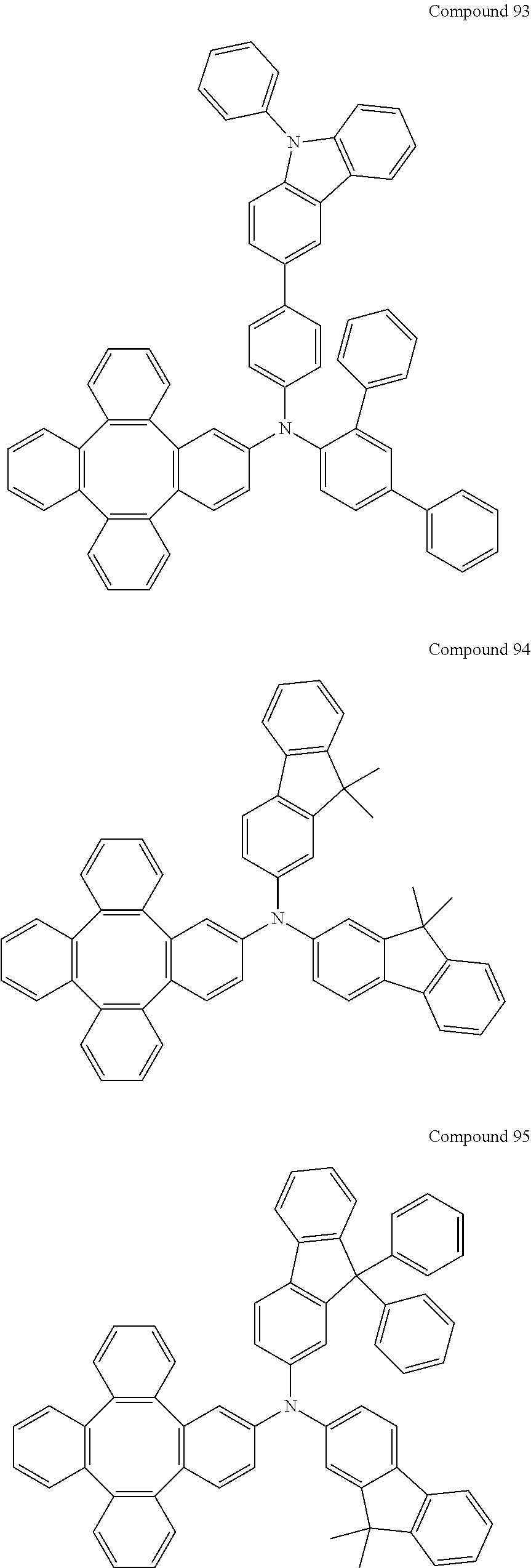


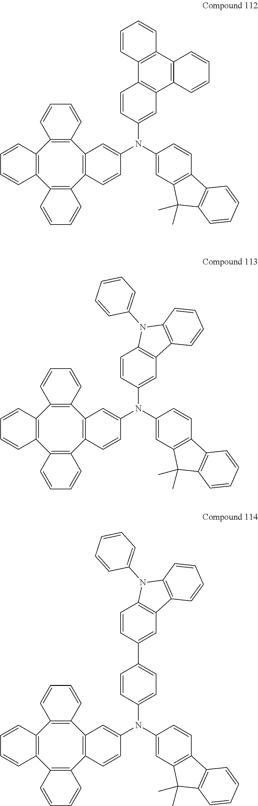


| TABLE 1 |
| Partial structure of device examples |
| Device ID | EBL | ||
| Example 1 | Compound 1 (50 Å) | ||
| Example 2 | Compound 6 (50 Å) | ||
| Example 3 | Compound 228 (50 Å) | ||


| TABLE 2 |
| Device data |
| Sub T | λmax | FWHM | Voltage | LE | |||
| Device ID | (° C.) | CIE (x, y) | (nm) | (nm) | (V) | (cd/A) | EQE (%) |
| Device | 231 | (0.336, 0.633) | 527 | 58.5 | 2.97 | 88.19 | 22.82 |
| Example 1 | |||||||
| Device | 234 | (0.337, 0.632) | 527 | 58.9 | 2.97 | 87.74 | 22.73 |
| Example 2 | |||||||
| Device | 258 | (0.335, 0.633) | 526 | 58.4 | 2.98 | 87.93 | 22.74 |
| Example 3 | |||||||
Claims (13)


Priority Applications (1)
| Application Number | Priority Date | Filing Date | Title |
|---|---|---|---|
| US16/223,135 US11512038B2 (en) | 2017-12-19 | 2018-12-18 | Tetraphenylene triarylamine compounds |
Applications Claiming Priority (2)
| Application Number | Priority Date | Filing Date | Title |
|---|---|---|---|
| US201762607331P | 2017-12-19 | 2017-12-19 | |
| US16/223,135 US11512038B2 (en) | 2017-12-19 | 2018-12-18 | Tetraphenylene triarylamine compounds |
Publications (2)
| Publication Number | Publication Date |
|---|---|
| US20190185412A1 US20190185412A1 (en) | 2019-06-20 |
| US11512038B2 true US11512038B2 (en) | 2022-11-29 |
Family
ID=66815602
Family Applications (1)
| Application Number | Title | Priority Date | Filing Date |
|---|---|---|---|
| US16/223,135 Active 2039-09-23 US11512038B2 (en) | 2017-12-19 | 2018-12-18 | Tetraphenylene triarylamine compounds |
Country Status (2)
| Country | Link |
|---|---|
| US (1) | US11512038B2 (en) |
| CN (1) | CN109928885B (en) |
Families Citing this family (9)
| Publication number | Priority date | Publication date | Assignee | Title |
|---|---|---|---|---|
| CN109651065B (en) | 2017-10-12 | 2022-11-29 | 北京夏禾科技有限公司 | Tetraortho-phenylene anthracene compounds |
| WO2020004235A1 (en) * | 2018-06-25 | 2020-01-02 | 保土谷化学工業株式会社 | Compound having triarylamine structure and electroluminescence device |
| CN112151682B (en) * | 2019-06-26 | 2023-08-22 | 夏禾科技(江苏)有限公司 | Organic electroluminescent device comprising hole blocking layer and electron transport layer |
| CN112778283B (en) * | 2019-11-08 | 2023-02-03 | 北京夏禾科技有限公司 | Organic electroluminescent material and device thereof |
| CN113410401B (en) * | 2020-03-16 | 2023-09-05 | 北京夏禾科技有限公司 | Organic electroluminescent devices containing deep LUMO hole-injecting materials and aromatic amine derivatives |
| CN112110825B (en) * | 2020-04-20 | 2022-02-11 | 陕西莱特光电材料股份有限公司 | Arylamine compound, electronic element using arylamine compound and electronic device |
| US12590102B2 (en) | 2020-05-22 | 2026-03-31 | Lg Chem, Ltd. | Compound and organic light emitting device comprising the same |
| JP2023011408A (en) * | 2021-07-12 | 2023-01-24 | 出光興産株式会社 | Compound, material for organic electroluminescent device, organic electroluminescent device, and electronic apparatus |
| CN116462673B (en) * | 2022-01-10 | 2025-10-14 | 北京夏禾科技有限公司 | A compound having a dehydrogenated linked ring skeleton |
Citations (40)
| Publication number | Priority date | Publication date | Assignee | Title |
|---|---|---|---|---|
| US5703436A (en) | 1994-12-13 | 1997-12-30 | The Trustees Of Princeton University | Transparent contacts for organic devices |
| US5707745A (en) | 1994-12-13 | 1998-01-13 | The Trustees Of Princeton University | Multicolor organic light emitting devices |
| US5844363A (en) | 1997-01-23 | 1998-12-01 | The Trustees Of Princeton Univ. | Vacuum deposited, non-polymeric flexible organic light emitting devices |
| US6097147A (en) | 1998-09-14 | 2000-08-01 | The Trustees Of Princeton University | Structure for high efficiency electroluminescent device |
| US20010006741A1 (en) | 1999-12-13 | 2001-07-05 | Nec Corporation | Organic electroluminescent device |
| US6303238B1 (en) | 1997-12-01 | 2001-10-16 | The Trustees Of Princeton University | OLEDs doped with phosphorescent compounds |
| US6416887B1 (en) * | 1998-11-11 | 2002-07-09 | Kabushiki Kaisha Toyota Chuo Kenkyusho | Organic electroluminescent element |
| CN1412864A (en) | 2001-10-18 | 2003-04-23 | 日本电气株式会社 | Organic thin film transistor |
| US20030118866A1 (en) * | 2001-10-30 | 2003-06-26 | Lg Electronics Inc. | Organic electroluminescent device |
| US20030230980A1 (en) | 2002-06-18 | 2003-12-18 | Forrest Stephen R | Very low voltage, high efficiency phosphorescent oled in a p-i-n structure |
| US20040124766A1 (en) * | 2002-10-24 | 2004-07-01 | Satoshi Nakagawa | Organic electroluminescent device |
| US20040174116A1 (en) | 2001-08-20 | 2004-09-09 | Lu Min-Hao Michael | Transparent electrodes |
| US20050112407A1 (en) | 2003-11-21 | 2005-05-26 | Fuji Photo Film Co., Ltd. | Organic electroluminescent device |
| US20060166034A1 (en) * | 2002-08-30 | 2006-07-27 | Canon Kabushiki Kaisha | Monoaminofluorene compound and organic light-emitting device using the same |
| US20070138953A1 (en) * | 2005-12-16 | 2007-06-21 | Fujifilm Corporation | Organic electroluminescent device |
| JP2007210964A (en) * | 2006-02-10 | 2007-08-23 | Tosoh Corp | Tetraphenylene derivative, use thereof, and production method thereof |
| US7279704B2 (en) | 2004-05-18 | 2007-10-09 | The University Of Southern California | Complexes with tridentate ligands |
| US20080213624A1 (en) * | 2007-02-28 | 2008-09-04 | E. I. Du Pont De Nemours And Company | Organic electronic device |
| US7968146B2 (en) | 2006-11-01 | 2011-06-28 | The Trustees Of Princeton University | Hybrid layers for use in coatings on electronic devices or other articles |
| US20130105771A1 (en) * | 2010-04-23 | 2013-05-02 | Dong-wan Ryu | Compound for optoelectronic device, organic light emitting diode including the same, and display including the organic light emitting diode |
| US20130207046A1 (en) * | 2010-09-15 | 2013-08-15 | Merck Patent Gmbh | Materials for organic electroluminescent devices |
| US20140131665A1 (en) | 2012-11-12 | 2014-05-15 | Universal Display Corporation | Organic Electroluminescent Device With Delayed Fluorescence |
| US20140158992A1 (en) | 2012-12-07 | 2014-06-12 | Universal Display Corporation | Carbazole Compounds For Delayed Fluorescence |
| US20150349273A1 (en) | 2014-06-03 | 2015-12-03 | Universal Display Corporation | Organic electroluminescent materials and devices |
| US20160013422A1 (en) | 2014-07-14 | 2016-01-14 | Universal Display Corporation | Organic electroluminescent materials and devices |
| US20160093810A1 (en) * | 2014-09-25 | 2016-03-31 | Samsung Display Co., Ltd. | Material for organic electroluminescent device and organic electroluminescent device using the same |
| WO2016181911A1 (en) | 2015-05-08 | 2016-11-17 | 株式会社リコー | Photoelectric conversion element |
| US20160343951A1 (en) | 2015-05-21 | 2016-11-24 | Universal Display Corporation | Organic electroluminescent materials and devices |
| US20160359122A1 (en) | 2015-06-04 | 2016-12-08 | Universal Display Corporation | Organic electroluminescent materials and devices |
| US20170018710A1 (en) * | 2014-03-07 | 2017-01-19 | Merck Patent Gmbh | Materials for electronic devices |
| US20170018721A1 (en) | 2015-07-15 | 2017-01-19 | Universal Display Corporation | Organic electroluminescent materials and devices |
| US20170077409A1 (en) | 2015-05-21 | 2017-03-16 | Universal Display Corporation | Organic electroluminescent materials and devices |
| US20170162816A1 (en) | 2015-12-07 | 2017-06-08 | Lg Display Co., Ltd. | Organic light emitting display apparatus |
| US20170271611A1 (en) * | 2014-08-22 | 2017-09-21 | Jian Li | Organic light-emitting diodes with fluorescent and phosphorescent emitters |
| US20180108844A1 (en) | 2016-10-17 | 2018-04-19 | Universal Display Corporation | Organic Electroluminescent Materials and Devices |
| US20190036031A1 (en) | 2017-07-26 | 2019-01-31 | Universal Display Corporation | Organic electroluminescent materials and devices |
| US20190100544A1 (en) | 2017-09-29 | 2019-04-04 | Chuanjun Xia | Organic luminescent materials containing tetraphenylene ligands |
| US20190115541A1 (en) | 2017-10-12 | 2019-04-18 | Chuanjun Xia | Tetraphenylene anthracene compounds |
| US20190123286A1 (en) | 2017-10-20 | 2019-04-25 | Chuanjun Xia | Indolocarbazole tetraphenylene compounds |
| CN110713492A (en) | 2018-07-13 | 2020-01-21 | 环球展览公司 | Organic Electroluminescent Materials and Devices |
-
2018
- 2018-12-07 CN CN201811493087.5A patent/CN109928885B/en active Active
- 2018-12-18 US US16/223,135 patent/US11512038B2/en active Active
Patent Citations (42)
| Publication number | Priority date | Publication date | Assignee | Title |
|---|---|---|---|---|
| US5707745A (en) | 1994-12-13 | 1998-01-13 | The Trustees Of Princeton University | Multicolor organic light emitting devices |
| US5703436A (en) | 1994-12-13 | 1997-12-30 | The Trustees Of Princeton University | Transparent contacts for organic devices |
| US5844363A (en) | 1997-01-23 | 1998-12-01 | The Trustees Of Princeton Univ. | Vacuum deposited, non-polymeric flexible organic light emitting devices |
| US6303238B1 (en) | 1997-12-01 | 2001-10-16 | The Trustees Of Princeton University | OLEDs doped with phosphorescent compounds |
| US6097147A (en) | 1998-09-14 | 2000-08-01 | The Trustees Of Princeton University | Structure for high efficiency electroluminescent device |
| US6416887B1 (en) * | 1998-11-11 | 2002-07-09 | Kabushiki Kaisha Toyota Chuo Kenkyusho | Organic electroluminescent element |
| US20010006741A1 (en) | 1999-12-13 | 2001-07-05 | Nec Corporation | Organic electroluminescent device |
| US20040174116A1 (en) | 2001-08-20 | 2004-09-09 | Lu Min-Hao Michael | Transparent electrodes |
| CN1412864A (en) | 2001-10-18 | 2003-04-23 | 日本电气株式会社 | Organic thin film transistor |
| US20030118866A1 (en) * | 2001-10-30 | 2003-06-26 | Lg Electronics Inc. | Organic electroluminescent device |
| US20030230980A1 (en) | 2002-06-18 | 2003-12-18 | Forrest Stephen R | Very low voltage, high efficiency phosphorescent oled in a p-i-n structure |
| US20060166034A1 (en) * | 2002-08-30 | 2006-07-27 | Canon Kabushiki Kaisha | Monoaminofluorene compound and organic light-emitting device using the same |
| US20040124766A1 (en) * | 2002-10-24 | 2004-07-01 | Satoshi Nakagawa | Organic electroluminescent device |
| US20050112407A1 (en) | 2003-11-21 | 2005-05-26 | Fuji Photo Film Co., Ltd. | Organic electroluminescent device |
| US7279704B2 (en) | 2004-05-18 | 2007-10-09 | The University Of Southern California | Complexes with tridentate ligands |
| US20070138953A1 (en) * | 2005-12-16 | 2007-06-21 | Fujifilm Corporation | Organic electroluminescent device |
| JP2007210964A (en) * | 2006-02-10 | 2007-08-23 | Tosoh Corp | Tetraphenylene derivative, use thereof, and production method thereof |
| US7968146B2 (en) | 2006-11-01 | 2011-06-28 | The Trustees Of Princeton University | Hybrid layers for use in coatings on electronic devices or other articles |
| US20080213624A1 (en) * | 2007-02-28 | 2008-09-04 | E. I. Du Pont De Nemours And Company | Organic electronic device |
| US20130105771A1 (en) * | 2010-04-23 | 2013-05-02 | Dong-wan Ryu | Compound for optoelectronic device, organic light emitting diode including the same, and display including the organic light emitting diode |
| US20130207046A1 (en) * | 2010-09-15 | 2013-08-15 | Merck Patent Gmbh | Materials for organic electroluminescent devices |
| US20140131665A1 (en) | 2012-11-12 | 2014-05-15 | Universal Display Corporation | Organic Electroluminescent Device With Delayed Fluorescence |
| US20140158992A1 (en) | 2012-12-07 | 2014-06-12 | Universal Display Corporation | Carbazole Compounds For Delayed Fluorescence |
| US20160060251A1 (en) | 2012-12-07 | 2016-03-03 | Universal Display Corporation | Organic electroluminescent materials and devices |
| US20170018710A1 (en) * | 2014-03-07 | 2017-01-19 | Merck Patent Gmbh | Materials for electronic devices |
| US20150349273A1 (en) | 2014-06-03 | 2015-12-03 | Universal Display Corporation | Organic electroluminescent materials and devices |
| US20160013422A1 (en) | 2014-07-14 | 2016-01-14 | Universal Display Corporation | Organic electroluminescent materials and devices |
| US20170271611A1 (en) * | 2014-08-22 | 2017-09-21 | Jian Li | Organic light-emitting diodes with fluorescent and phosphorescent emitters |
| US20160093810A1 (en) * | 2014-09-25 | 2016-03-31 | Samsung Display Co., Ltd. | Material for organic electroluminescent device and organic electroluminescent device using the same |
| WO2016181911A1 (en) | 2015-05-08 | 2016-11-17 | 株式会社リコー | Photoelectric conversion element |
| US20160343951A1 (en) | 2015-05-21 | 2016-11-24 | Universal Display Corporation | Organic electroluminescent materials and devices |
| US20170077409A1 (en) | 2015-05-21 | 2017-03-16 | Universal Display Corporation | Organic electroluminescent materials and devices |
| US20160359122A1 (en) | 2015-06-04 | 2016-12-08 | Universal Display Corporation | Organic electroluminescent materials and devices |
| US20170018721A1 (en) | 2015-07-15 | 2017-01-19 | Universal Display Corporation | Organic electroluminescent materials and devices |
| CN106848070A (en) | 2015-12-07 | 2017-06-13 | 乐金显示有限公司 | Oganic light-emitting display device |
| US20170162816A1 (en) | 2015-12-07 | 2017-06-08 | Lg Display Co., Ltd. | Organic light emitting display apparatus |
| US20180108844A1 (en) | 2016-10-17 | 2018-04-19 | Universal Display Corporation | Organic Electroluminescent Materials and Devices |
| US20190036031A1 (en) | 2017-07-26 | 2019-01-31 | Universal Display Corporation | Organic electroluminescent materials and devices |
| US20190100544A1 (en) | 2017-09-29 | 2019-04-04 | Chuanjun Xia | Organic luminescent materials containing tetraphenylene ligands |
| US20190115541A1 (en) | 2017-10-12 | 2019-04-18 | Chuanjun Xia | Tetraphenylene anthracene compounds |
| US20190123286A1 (en) | 2017-10-20 | 2019-04-25 | Chuanjun Xia | Indolocarbazole tetraphenylene compounds |
| CN110713492A (en) | 2018-07-13 | 2020-01-21 | 环球展览公司 | Organic Electroluminescent Materials and Devices |
Non-Patent Citations (7)
| Title |
|---|
| C.W. Tang et al. "Organic electroluminescent diodes", Appl. Phys. Ltt. 51, 913 (1987); doi: 10.1063/1.98799. |
| CN Office Action, including Search Report, dated Jul. 19, 2021 for CN Application No. 201811493087, 7 pages. |
| English Translation of CN Office Action, including Search Report, dated Jul. 19, 2021 for CN Application No. 201811493087, 7 pages. |
| Hiroki Uoyama et al. "Highli efficient organic light-emitting diodes from delayed fluorescence", doi:10.1038/nature 11687, 234, Nature, vol. 492, Dec. 13, 2012. |
| National Science Review, 4: 892-916, (2017). (Year: 2017). * |
| Pan et al., Beilstein Journal of Organic Chemistry, (2016), vol. 12, pp. 1302-1308. (Year: 2016). * |
| Shulei Pan, et al., "Synthesis of 2-substituted tetraphenylenes via transitionmetal-catalyzed derivatization of tetraphenylene", Beilstein Journal Of Organic Chemistry, 2016, 12, 1302-1308. |
Also Published As
| Publication number | Publication date |
|---|---|
| CN109928885B (en) | 2022-11-29 |
| US20190185412A1 (en) | 2019-06-20 |
| CN109928885A (en) | 2019-06-25 |
Similar Documents
| Publication | Publication Date | Title |
|---|---|---|
| US12156466B2 (en) | Organic electroluminescent material and device | |
| US11239430B2 (en) | Boron and nitrogen containing heterocyclic compounds | |
| US11349080B2 (en) | Organic electroluminescent materials and devices | |
| US10998506B2 (en) | Boron containing heterocyclic compound for OLEDs, an organic light-emitting device, and a formulation comprising the boron-containing heterocyclic compound | |
| US11839147B2 (en) | Hole injection layer and charge generation layer containing a truxene based compound | |
| US20200203631A1 (en) | Organic electroluminescent device comprising a dopant material and multiple host materials | |
| US20200099000A1 (en) | Organic luminescent materials containing novel ancillary ligands | |
| US11498937B2 (en) | Organic luminescent material including 3-deuterium-substituted isoquinoline ligand | |
| US20190194234A1 (en) | Metal complexes containing heterocycle substituted ligands, and electroluminescent devices and formulations containing the complexes | |
| US11581498B2 (en) | Organic luminescent material containing 6-silyl-substituted isoquinoline ligand | |
| US11512038B2 (en) | Tetraphenylene triarylamine compounds | |
| US11201290B2 (en) | Tetraphenylene anthracene compounds | |
| US11993617B2 (en) | Organic luminescent material having an ancillary ligand with a partially fluorine-substituted substituent | |
| US11349081B2 (en) | Azaindolocarbazole compounds | |
| US10978645B2 (en) | Indolocarbazole tetraphenylene compounds | |
| US20190077818A1 (en) | Organic luminescent materials containing fluorine ancillary ligands | |
| US11708356B2 (en) | Organic electroluminescent materials and devices | |
| US12201014B2 (en) | Metal complex, electroluminescent device including the same, and use thereof | |
| US10957869B2 (en) | Organic luminescent materials containing cycloalkyl ancillary ligands | |
| US11325934B2 (en) | Organic luminescent materials containing tetraphenylene ligands | |
| US20190165278A1 (en) | Thiophene-containing triarylamine compounds | |
| US20190109284A1 (en) | Crosslinkable deuterated charge transporting compound, an organic electroluminescent device comprising the compound, and a solution formulation | |
| US20230167097A1 (en) | Heterocyclic compound having cyano-substitution | |
| US20220165968A1 (en) | Organic electroluminescent material and device thereof | |
| US12145954B2 (en) | Silicon-containing electron transporting material and its application |
Legal Events
| Date | Code | Title | Description |
|---|---|---|---|
| FEPP | Fee payment procedure |
Free format text: ENTITY STATUS SET TO UNDISCOUNTED (ORIGINAL EVENT CODE: BIG.); ENTITY STATUS OF PATENT OWNER: SMALL ENTITY |
|
| AS | Assignment |
Owner name: BEIJING SUMMER SPROUT TECHNOLOGY CO., LTD., CHINA Free format text: ASSIGNMENT OF ASSIGNORS INTEREST;ASSIGNOR:XIA, CHUANJUN;REEL/FRAME:047855/0724 Effective date: 20181221 |
|
| FEPP | Fee payment procedure |
Free format text: ENTITY STATUS SET TO SMALL (ORIGINAL EVENT CODE: SMAL); ENTITY STATUS OF PATENT OWNER: SMALL ENTITY |
|
| STPP | Information on status: patent application and granting procedure in general |
Free format text: DOCKETED NEW CASE - READY FOR EXAMINATION |
|
| STPP | Information on status: patent application and granting procedure in general |
Free format text: NON FINAL ACTION MAILED |
|
| STPP | Information on status: patent application and granting procedure in general |
Free format text: RESPONSE TO NON-FINAL OFFICE ACTION ENTERED AND FORWARDED TO EXAMINER |
|
| STPP | Information on status: patent application and granting procedure in general |
Free format text: FINAL REJECTION MAILED |
|
| STPP | Information on status: patent application and granting procedure in general |
Free format text: DOCKETED NEW CASE - READY FOR EXAMINATION |
|
| STPP | Information on status: patent application and granting procedure in general |
Free format text: NON FINAL ACTION MAILED |
|
| STPP | Information on status: patent application and granting procedure in general |
Free format text: RESPONSE TO NON-FINAL OFFICE ACTION ENTERED AND FORWARDED TO EXAMINER |
|
| STPP | Information on status: patent application and granting procedure in general |
Free format text: NOTICE OF ALLOWANCE MAILED -- APPLICATION RECEIVED IN OFFICE OF PUBLICATIONS |
|
| STPP | Information on status: patent application and granting procedure in general |
Free format text: PUBLICATIONS -- ISSUE FEE PAYMENT RECEIVED |
|
| STPP | Information on status: patent application and granting procedure in general |
Free format text: PUBLICATIONS -- ISSUE FEE PAYMENT VERIFIED |
|
| STCF | Information on status: patent grant |
Free format text: PATENTED CASE |