US11708356B2 - Organic electroluminescent materials and devices - Google Patents
Organic electroluminescent materials and devices Download PDFInfo
- Publication number
- US11708356B2 US11708356B2 US16/803,280 US202016803280A US11708356B2 US 11708356 B2 US11708356 B2 US 11708356B2 US 202016803280 A US202016803280 A US 202016803280A US 11708356 B2 US11708356 B2 US 11708356B2
- Authority
- US
- United States
- Prior art keywords
- group
- carbon atoms
- substituted
- unsubstituted
- compound
- Prior art date
- Legal status (The legal status is an assumption and is not a legal conclusion. Google has not performed a legal analysis and makes no representation as to the accuracy of the status listed.)
- Active, expires
Links
Images


Classifications
-
- C—CHEMISTRY; METALLURGY
- C07—ORGANIC CHEMISTRY
- C07D—HETEROCYCLIC COMPOUNDS
- C07D403/00—Heterocyclic compounds containing two or more hetero rings, having nitrogen atoms as the only ring hetero atoms, not provided for by group C07D401/00
- C07D403/02—Heterocyclic compounds containing two or more hetero rings, having nitrogen atoms as the only ring hetero atoms, not provided for by group C07D401/00 containing two hetero rings
- C07D403/04—Heterocyclic compounds containing two or more hetero rings, having nitrogen atoms as the only ring hetero atoms, not provided for by group C07D401/00 containing two hetero rings directly linked by a ring-member-to-ring-member bond
-
- C—CHEMISTRY; METALLURGY
- C07—ORGANIC CHEMISTRY
- C07D—HETEROCYCLIC COMPOUNDS
- C07D403/00—Heterocyclic compounds containing two or more hetero rings, having nitrogen atoms as the only ring hetero atoms, not provided for by group C07D401/00
- C07D403/02—Heterocyclic compounds containing two or more hetero rings, having nitrogen atoms as the only ring hetero atoms, not provided for by group C07D401/00 containing two hetero rings
- C07D403/10—Heterocyclic compounds containing two or more hetero rings, having nitrogen atoms as the only ring hetero atoms, not provided for by group C07D401/00 containing two hetero rings linked by a carbon chain containing aromatic rings
-
- C—CHEMISTRY; METALLURGY
- C07—ORGANIC CHEMISTRY
- C07D—HETEROCYCLIC COMPOUNDS
- C07D405/00—Heterocyclic compounds containing both one or more hetero rings having oxygen atoms as the only ring hetero atoms, and one or more rings having nitrogen as the only ring hetero atom
- C07D405/02—Heterocyclic compounds containing both one or more hetero rings having oxygen atoms as the only ring hetero atoms, and one or more rings having nitrogen as the only ring hetero atom containing two hetero rings
- C07D405/04—Heterocyclic compounds containing both one or more hetero rings having oxygen atoms as the only ring hetero atoms, and one or more rings having nitrogen as the only ring hetero atom containing two hetero rings directly linked by a ring-member-to-ring-member bond
-
- C—CHEMISTRY; METALLURGY
- C07—ORGANIC CHEMISTRY
- C07D—HETEROCYCLIC COMPOUNDS
- C07D405/00—Heterocyclic compounds containing both one or more hetero rings having oxygen atoms as the only ring hetero atoms, and one or more rings having nitrogen as the only ring hetero atom
- C07D405/14—Heterocyclic compounds containing both one or more hetero rings having oxygen atoms as the only ring hetero atoms, and one or more rings having nitrogen as the only ring hetero atom containing three or more hetero rings
-
- C—CHEMISTRY; METALLURGY
- C09—DYES; PAINTS; POLISHES; NATURAL RESINS; ADHESIVES; COMPOSITIONS NOT OTHERWISE PROVIDED FOR; APPLICATIONS OF MATERIALS NOT OTHERWISE PROVIDED FOR
- C09K—MATERIALS FOR MISCELLANEOUS APPLICATIONS, NOT PROVIDED FOR ELSEWHERE
- C09K11/00—Luminescent materials, e.g. electroluminescent or chemiluminescent
- C09K11/06—Luminescent materials, e.g. electroluminescent or chemiluminescent containing organic luminescent materials
-
- H—ELECTRICITY
- H10—SEMICONDUCTOR DEVICES; ELECTRIC SOLID-STATE DEVICES NOT OTHERWISE PROVIDED FOR
- H10K—ORGANIC ELECTRIC SOLID-STATE DEVICES
- H10K30/00—Organic devices sensitive to infrared radiation, light, electromagnetic radiation of shorter wavelength or corpuscular radiation
- H10K30/30—Organic devices sensitive to infrared radiation, light, electromagnetic radiation of shorter wavelength or corpuscular radiation comprising bulk heterojunctions, e.g. interpenetrating networks of donor and acceptor material domains
- H10K30/353—Organic devices sensitive to infrared radiation, light, electromagnetic radiation of shorter wavelength or corpuscular radiation comprising bulk heterojunctions, e.g. interpenetrating networks of donor and acceptor material domains comprising blocking layers, e.g. exciton blocking layers
-
- H—ELECTRICITY
- H10—SEMICONDUCTOR DEVICES; ELECTRIC SOLID-STATE DEVICES NOT OTHERWISE PROVIDED FOR
- H10K—ORGANIC ELECTRIC SOLID-STATE DEVICES
- H10K85/00—Organic materials used in the body or electrodes of devices covered by this subclass
- H10K85/60—Organic compounds having low molecular weight
- H10K85/615—Polycyclic condensed aromatic hydrocarbons, e.g. anthracene
- H10K85/622—Polycyclic condensed aromatic hydrocarbons, e.g. anthracene containing four rings, e.g. pyrene
-
- H—ELECTRICITY
- H10—SEMICONDUCTOR DEVICES; ELECTRIC SOLID-STATE DEVICES NOT OTHERWISE PROVIDED FOR
- H10K—ORGANIC ELECTRIC SOLID-STATE DEVICES
- H10K85/00—Organic materials used in the body or electrodes of devices covered by this subclass
- H10K85/60—Organic compounds having low molecular weight
- H10K85/649—Aromatic compounds comprising a hetero atom
- H10K85/654—Aromatic compounds comprising a hetero atom comprising only nitrogen as heteroatom
-
- H—ELECTRICITY
- H10—SEMICONDUCTOR DEVICES; ELECTRIC SOLID-STATE DEVICES NOT OTHERWISE PROVIDED FOR
- H10K—ORGANIC ELECTRIC SOLID-STATE DEVICES
- H10K85/00—Organic materials used in the body or electrodes of devices covered by this subclass
- H10K85/60—Organic compounds having low molecular weight
- H10K85/649—Aromatic compounds comprising a hetero atom
- H10K85/657—Polycyclic condensed heteroaromatic hydrocarbons
- H10K85/6572—Polycyclic condensed heteroaromatic hydrocarbons comprising only nitrogen in the heteroaromatic polycondensed ring system, e.g. phenanthroline or carbazole
-
- H—ELECTRICITY
- H10—SEMICONDUCTOR DEVICES; ELECTRIC SOLID-STATE DEVICES NOT OTHERWISE PROVIDED FOR
- H10K—ORGANIC ELECTRIC SOLID-STATE DEVICES
- H10K85/00—Organic materials used in the body or electrodes of devices covered by this subclass
- H10K85/60—Organic compounds having low molecular weight
- H10K85/649—Aromatic compounds comprising a hetero atom
- H10K85/657—Polycyclic condensed heteroaromatic hydrocarbons
- H10K85/6574—Polycyclic condensed heteroaromatic hydrocarbons comprising only oxygen in the heteroaromatic polycondensed ring system, e.g. cumarine dyes
-
- C—CHEMISTRY; METALLURGY
- C09—DYES; PAINTS; POLISHES; NATURAL RESINS; ADHESIVES; COMPOSITIONS NOT OTHERWISE PROVIDED FOR; APPLICATIONS OF MATERIALS NOT OTHERWISE PROVIDED FOR
- C09K—MATERIALS FOR MISCELLANEOUS APPLICATIONS, NOT PROVIDED FOR ELSEWHERE
- C09K2211/00—Chemical nature of organic luminescent or tenebrescent compounds
- C09K2211/10—Non-macromolecular compounds
- C09K2211/1003—Carbocyclic compounds
- C09K2211/1007—Non-condensed systems
-
- C—CHEMISTRY; METALLURGY
- C09—DYES; PAINTS; POLISHES; NATURAL RESINS; ADHESIVES; COMPOSITIONS NOT OTHERWISE PROVIDED FOR; APPLICATIONS OF MATERIALS NOT OTHERWISE PROVIDED FOR
- C09K—MATERIALS FOR MISCELLANEOUS APPLICATIONS, NOT PROVIDED FOR ELSEWHERE
- C09K2211/00—Chemical nature of organic luminescent or tenebrescent compounds
- C09K2211/10—Non-macromolecular compounds
- C09K2211/1003—Carbocyclic compounds
- C09K2211/1011—Condensed systems
-
- C—CHEMISTRY; METALLURGY
- C09—DYES; PAINTS; POLISHES; NATURAL RESINS; ADHESIVES; COMPOSITIONS NOT OTHERWISE PROVIDED FOR; APPLICATIONS OF MATERIALS NOT OTHERWISE PROVIDED FOR
- C09K—MATERIALS FOR MISCELLANEOUS APPLICATIONS, NOT PROVIDED FOR ELSEWHERE
- C09K2211/00—Chemical nature of organic luminescent or tenebrescent compounds
- C09K2211/10—Non-macromolecular compounds
- C09K2211/1018—Heterocyclic compounds
- C09K2211/1025—Heterocyclic compounds characterised by ligands
- C09K2211/1029—Heterocyclic compounds characterised by ligands containing one nitrogen atom as the heteroatom
-
- C—CHEMISTRY; METALLURGY
- C09—DYES; PAINTS; POLISHES; NATURAL RESINS; ADHESIVES; COMPOSITIONS NOT OTHERWISE PROVIDED FOR; APPLICATIONS OF MATERIALS NOT OTHERWISE PROVIDED FOR
- C09K—MATERIALS FOR MISCELLANEOUS APPLICATIONS, NOT PROVIDED FOR ELSEWHERE
- C09K2211/00—Chemical nature of organic luminescent or tenebrescent compounds
- C09K2211/10—Non-macromolecular compounds
- C09K2211/1018—Heterocyclic compounds
- C09K2211/1025—Heterocyclic compounds characterised by ligands
- C09K2211/1059—Heterocyclic compounds characterised by ligands containing three nitrogen atoms as heteroatoms
-
- C—CHEMISTRY; METALLURGY
- C09—DYES; PAINTS; POLISHES; NATURAL RESINS; ADHESIVES; COMPOSITIONS NOT OTHERWISE PROVIDED FOR; APPLICATIONS OF MATERIALS NOT OTHERWISE PROVIDED FOR
- C09K—MATERIALS FOR MISCELLANEOUS APPLICATIONS, NOT PROVIDED FOR ELSEWHERE
- C09K2211/00—Chemical nature of organic luminescent or tenebrescent compounds
- C09K2211/10—Non-macromolecular compounds
- C09K2211/1018—Heterocyclic compounds
- C09K2211/1025—Heterocyclic compounds characterised by ligands
- C09K2211/1088—Heterocyclic compounds characterised by ligands containing oxygen as the only heteroatom
-
- H—ELECTRICITY
- H10—SEMICONDUCTOR DEVICES; ELECTRIC SOLID-STATE DEVICES NOT OTHERWISE PROVIDED FOR
- H10K—ORGANIC ELECTRIC SOLID-STATE DEVICES
- H10K2101/00—Properties of the organic materials covered by group H10K85/00
- H10K2101/10—Triplet emission
-
- H—ELECTRICITY
- H10—SEMICONDUCTOR DEVICES; ELECTRIC SOLID-STATE DEVICES NOT OTHERWISE PROVIDED FOR
- H10K—ORGANIC ELECTRIC SOLID-STATE DEVICES
- H10K50/00—Organic light-emitting devices
- H10K50/10—OLEDs or polymer light-emitting diodes [PLED]
- H10K50/11—OLEDs or polymer light-emitting diodes [PLED] characterised by the electroluminescent [EL] layers
-
- H—ELECTRICITY
- H10—SEMICONDUCTOR DEVICES; ELECTRIC SOLID-STATE DEVICES NOT OTHERWISE PROVIDED FOR
- H10K—ORGANIC ELECTRIC SOLID-STATE DEVICES
- H10K50/00—Organic light-emitting devices
- H10K50/10—OLEDs or polymer light-emitting diodes [PLED]
- H10K50/18—Carrier blocking layers
-
- H—ELECTRICITY
- H10—SEMICONDUCTOR DEVICES; ELECTRIC SOLID-STATE DEVICES NOT OTHERWISE PROVIDED FOR
- H10K—ORGANIC ELECTRIC SOLID-STATE DEVICES
- H10K85/00—Organic materials used in the body or electrodes of devices covered by this subclass
- H10K85/30—Coordination compounds
- H10K85/341—Transition metal complexes, e.g. Ru(II)polypyridine complexes
- H10K85/342—Transition metal complexes, e.g. Ru(II)polypyridine complexes comprising iridium
-
- Y—GENERAL TAGGING OF NEW TECHNOLOGICAL DEVELOPMENTS; GENERAL TAGGING OF CROSS-SECTIONAL TECHNOLOGIES SPANNING OVER SEVERAL SECTIONS OF THE IPC; TECHNICAL SUBJECTS COVERED BY FORMER USPC CROSS-REFERENCE ART COLLECTIONS [XRACs] AND DIGESTS
- Y02—TECHNOLOGIES OR APPLICATIONS FOR MITIGATION OR ADAPTATION AGAINST CLIMATE CHANGE
- Y02E—REDUCTION OF GREENHOUSE GAS [GHG] EMISSIONS, RELATED TO ENERGY GENERATION, TRANSMISSION OR DISTRIBUTION
- Y02E10/00—Energy generation through renewable energy sources
- Y02E10/50—Photovoltaic [PV] energy
- Y02E10/549—Organic PV cells
Definitions
- the present disclosure relates to compounds for organic electronic device, such as organic electroluminescent device. More specifically, it relates to novel carbazole compounds, and organic electroluminescent devices and a compound formulation comprising the same.
- Organic electronic devices include, but are not limited to, the following types: organic light-emitting diodes (OLEDs), organic field-effect transistors (O-FETs), organic light-emitting transistors (OLETs), organic photovoltaic devices (OPVs), dye-sensitized solar cells (DSSCs), organic optical detectors, organic photoreceptors, organic field-quench devices (OFQDs), light-emitting electrochemical cells (LECs), organic laser diodes and organic plasmon emitting devices.
- OLEDs organic light-emitting diodes
- O-FETs organic field-effect transistors
- OLETs organic light-emitting transistors
- OLEDs organic photovoltaic devices
- OFQDs organic field-quench devices
- LECs light-emitting electrochemical cells
- organic laser diodes and organic plasmon emitting devices.
- OLEDs organic light-emitting diodes
- O-FETs organic field-effect transistors
- OLED can be categorized as three different types according to its emitting mechanism.
- the OLED invented by Tang and van Slyke is a fluorescent OLED. It only utilizes singlet emission. The triplets generated in the device are wasted through nonradiative decay channels. Therefore, the internal quantum efficiency (IQE) of a fluorescent OLED is only 25%. This limitation hindered the commercialization of OLED.
- IQE internal quantum efficiency
- Forrest and Thompson reported phosphorescent OLED, which uses triplet emission from heave metal containing complexes as the emitter. As a result, both singlet and triplets can be harvested, achieving 100% IQE.
- the discovery and development of phosphorescent OLED contributed directly to the commercialization of active-matrix OLED (AMOLED) due to its high efficiency.
- AMOLED active-matrix OLED
- Adachi achieved high efficiency through thermally activated delayed fluorescence (TADF) of organic compounds. These emitters have small singlet-triplet gap that makes the transition from triplet back to singlet possible. In the TADF device, the triplet excitons can go through reverse intersystem crossing to generate singlet excitons, resulting in high IQE.
- TADF thermally activated delayed fluorescence
- the emitting color of an OLED can be achieved by emitter structural design.
- An OLED may comprise one emitting layer or a plurality of emitting layers to achieve desired spectrum.
- phosphorescent emitters have successfully reached commercialization. Blue phosphorescent device still suffers from non-saturated blue color, short device lifetime, and high operating voltage.
- Commercial full-color OLED displays normally adopt a hybrid strategy, using fluorescent blue and phosphorescent yellow, or red and green. At present, efficiency roll-off of phosphorescent OLEDs at high brightness remains a problem. In addition, it is desirable to have more saturated emitting color, higher efficiency, and longer device lifetime.
- the carbazole-based organic semiconductor materials have a wide range of application in optoelectronic devices due to their superior optoelectronic properties, redox properties, stability and etc.
- WO2013100538A1 disclosed carbazole compounds of the following structure
- the inventor of this application noticed various advantages of the compound obtained by combining carbazole with an aza six-membered aromatic ring such as pyridine, pyrimidine, and triazine, but it did not explicitly recognize the unique advantages of the triazine structure.
- an aza six-membered aromatic ring such as pyridine, pyrimidine, and triazine
- KR1020180060474A, EP2991128A1 and US20150228908A1 all have disclosed compounds in which the aza-ring structure such as triazine is connected to the 4-position of the carbazole ring through a single bond or a (hetero) arylene-based linking group.
- KR1020180060474A requires that a carbazole group further be connected to the carbazole unit, which may lead to unfavorable results of excessively enhanced hole transporting capabilities.
- EP2991128A1 mainly focuses on the combination use of a compound having a triazine substitution at the 4-position of carbazole and a specific second host compound having a bicarbazole and a benzothienopyrimidine or benzofuropyrimidine structure.
- US20150228908A1 also noticed the advantage of introducing an aza-aromatic ring at the 4-position of carbazole. It uses a series of aza-aromatic ring structures such as triazine, pyrimidine, quinoxaline, pyrimidopyrimidine, and pyrazinoimidazole. It is also unconscious about the advantages of substitution to other positions on the carbazole ring, especially the 2-position.
- carbazole-based organic semiconductor materials reported currently have certain limitations in optoelectronic devices such as carrier transporting capabilities, efficiency, and lifetime. Therefore, the application potential of such materials deserves further research and development.
- the present invention discloses a new carbazole compound, which can improve the lifetime of a device and provide better device performance.
- the present disclosure aims to provide a series of compounds with novel carbazole structure to solve at least part of the above problems.
- the compound can be used as host material, hole blocking material in an organic electroluminescent device. These new compounds can provide better device performance, such as device performance of very low driving voltage, high efficiency, and long lifetime.
- R a is selected from biphenyl, terphenyl, naphthyl, phenanthryl, triphenylene, fluorenyl, dibenzofuranyl;
- n is the number of R b , n is selected from 1, 2, 3 or 4; when n ⁇ 2, the R b is selected from the same or different structures, each of R b is independently selected from the group consisting of: hydrogen, deuterium, phenyl, biphenyl and terphenyl;
- R c , R d and R e are each independently selected from the group consisting of hydrogen, deuterium, halogen, a substituted or unsubstituted alkyl group having 1 to 20 carbon atoms, a substituted or unsubstituted cycloalkyl group having 3 to 20 ring carbon atoms, a substituted or unsubstituted heteroalkyl group having 1 to 20 carbon atoms, a substituted or unsubstituted arylalkyl group having 7 to 30 carbon atoms, a substituted or unsubstituted alkoxy group having 1 to 20 carbon atoms, a substituted or unsubstituted aryloxy group having 6 to 30 carbon atoms, a substituted or unsubstituted aryl group having 6 to 30 carbon atoms, a substituted or unsubstituted heteroaryl group having 3 to 30 carbon atoms, a substituted or unsubstituted alkylsilyl group having 3
- R 1 has the structure of Formula 2:
- L is a single bond, or a substituted or unsubstituted arylene having 6 to 60 carbon atoms;
- R 2 and R 3 are each independently selected from the group consisting of hydrogen, deuterium, halogen, a substituted or unsubstituted alkyl group having 1 to 20 carbon atoms, a substituted or unsubstituted cycloalkyl group having 3 to 20 ring carbon atoms, a substituted or unsubstituted heteroalkyl group having 1 to 20 carbon atoms, a substituted or unsubstituted arylalkyl group having 7 to 30 carbon atoms, a substituted or unsubstituted alkoxy group having 1 to 20 carbon atoms, a substituted or unsubstituted aryloxy group having 6 to 30 carbon atoms, a substituted or unsubstituted aryl group having 6 to 30 carbon atoms, a substituted or unsubstituted alkylsilyl group having 3 to 20 carbon atoms, a substituted or unsubstituted arylsilyl group having 6 to 20 carbon
- R 2 and R 3 are selected from a substituted group in the group
- the substitution in the substituted group is selected from deuterium, halogen, an unsubstituted alkyl group having 1 to 20 carbon atoms, an unsubstituted cycloalkyl group having 3 to 20 ring carbon atoms, an unsubstituted heteroalkyl group having 1 to 20 carbon atoms, an unsubstituted arylalkyl group having 7 to 30 carbon atoms, an unsubstituted alkoxy group having 1 to 20 carbon atoms, an unsubstituted aryl group having 6 to 30 carbon atoms, and combinations thereof.
- an electroluminescent device which comprises an anode, a cathode, and an organic layer disposed between the anode and the cathode, wherein the organic layer comprising the compound having the structure of Formula 1 described above.
- a compound formulation comprising the compound having the structure of Formula 1 described above is also disclosed.
- the compound having a novel carbazole structure disclosed in the present disclosure can be used as host material, hole blocking material in an organic electroluminescent device. Compared with existing compounds, these new compounds can provide better device performance, such as very low drive voltage, high efficiency, and long lifetime.
- FIG. 1 schematically shows an organic light emitting device that can incorporate the compound and compound formulation disclosed herein.
- FIG. 2 schematically shows another organic light emitting device that can incorporate the compound and compound formulation disclosed herein.
- FIG. 3 shows the Structural Formula 1 of the compound disclosed herein.
- FIG. 1 schematically shows the organic light emitting device 100 without limitation. The figures are not necessarily drawn to scale. Some of the layers in the figures may also be omitted as needed.
- Device 100 may include a substrate 101 , an anode 110 , a hole injection layer 120 , a hole transport layer 130 , an electron blocking layer 140 , an emissive layer 150 , a hole blocking layer 160 , an electron transport layer 170 , an electron injection layer 180 and a cathode 190 .
- Device 100 may be fabricated by depositing the layers described in order. The properties and functions of these various layers, as well as example materials, are described in more detail in U.S. Pat. No. 7,279,704 at cols. 6-10, the contents of which are incorporated by reference herein in its entirety.
- each of these layers are available.
- a flexible and transparent substrate-anode combination is disclosed in U.S. Pat. No. 5,844,363, which is incorporated by reference herein in its entirety.
- An example of a p-doped hole transport layer is m-MTDATA doped with F 4 -TCNQ at a molar ratio of 50:1, as disclosed in U.S. Patent Application Publication No. 2003/0230980, which is incorporated by reference herein in its entirety.
- host materials are disclosed in U.S. Pat. No. 6,303,238 to Thompson et al., which is incorporated by reference herein in its entirety.
- An example of an n-doped electron transport layer is BPhen doped with Li at a molar ratio of 1:1, as disclosed in U.S. Patent Application Publication No. 2003/0230980, which is incorporated by reference herein in its entirety.
- the theory and use of blocking layers is described in more detail in U.S. Pat. No. 6,097,147 and U.S. Patent Application Publication No.
- Functional OLEDs may be achieved by combining the various layers described in different ways, or layers may be omitted entirely. It may also include other layers not specifically described. Within each layer, a single material or a mixture of multiple materials may be used to achieve optimum performance. Any functional layer may include several sublayers. For example, the emissive layer may have two layers of different emitting materials to achieve desired emission spectrum.
- an OLED may be described as having an “organic layer” disposed between a cathode and an anode.
- This organic layer may comprise a single layer or multiple layers.
- FIG. 2 schematically shows the organic light emitting device 200 without limitation.
- FIG. 2 differs from FIG. 1 in that the organic light emitting device include a barrier layer 102 , which is above the cathode 190 , to protect it from harmful species from the environment such as moisture and oxygen. Any material that may provide the barrier function may be used as the barrier layer such as glass and organic-inorganic hybrid layers.
- the barrier layer should be placed directly or indirectly outside of the OLED device. Multilayer thin film encapsulation was described in U.S. Pat. No. 7,968,146, which is herein incorporated by reference in its entirety.
- Devices fabricated in accordance with embodiments of the present disclosure may be incorporated into a wide variety of consumer products that have one or more of the electronic component modules (or units) incorporated therein.
- Some examples of such consumer products include flat panel displays, monitors, medical monitors, televisions, billboards, lights for interior or exterior illumination and/or signaling, heads-up displays, fully or partially transparent displays, flexible displays, smart phones, tablets, phablets, wearable devices, smart watches, laptop computers, digital cameras, camcorders, viewfinders, micro-displays, 3-D displays, vehicles displays, and vehicle tail lights.
- top means furthest away from the substrate, while “bottom” means closest to the substrate.
- first layer is described as “disposed over” a second layer, the first layer is disposed further away from substrate. There may be other layers between the first and second layer, unless it is specified that the first layer is “in contact with” the second layer.
- a cathode may be described as “disposed over” an anode, even though there are various organic layers in between.
- solution processable means capable of being dissolved, dispersed, or transported in and/or deposited from a liquid medium, either in solution or suspension form.
- a ligand may be referred to as “photoactive” when it is believed that the ligand directly contributes to the photoactive properties of an emissive material.
- a ligand may be referred to as “ancillary” when it is believed that the ligand does not contribute to the photoactive properties of an emissive material, although an ancillary ligand may alter the properties of a photoactive ligand.
- IQE internal quantum efficiency
- P-type delayed fluorescence is generated from triplet-triplet annihilation (TTA).
- E-type delayed fluorescence does not rely on the collision of two triplets, but rather on the transition between the triplet states and the singlet excited states.
- Compounds that are capable of generating E-type delayed fluorescence are required to have very small singlet-triplet gaps to convert between energy states.
- Thermal energy may activate the transition from the triplet state back to the singlet state.
- This type of delayed fluorescence is also known as thermally activated delayed fluorescence (TADF).
- TADF thermally activated delayed fluorescence
- a distinctive feature of TADF is that the delayed component increases as temperature rises. If the reverse intersystem crossing rate is fast enough to minimize the non-radiative decay from the triplet state, the fraction of back populated singlet excited states may potentially reach 75%. The total singlet fraction may be 100%, far exceeding 25% of the spin statistics limit for electrically generated excitons.
- E-type delayed fluorescence characteristics may be found in an exciplex system or in a single compound. Without being bound by theory, it is believed that E-type delayed fluorescence requires the luminescent material to have a small singlet-triplet energy gap ( ⁇ E S-T ).
- Organic, non-metal containing, donor-acceptor luminescent materials may be able to achieve this.
- the emission in these materials is often characterized as a donor-acceptor charge-transfer (CT) type emission.
- CT charge-transfer
- the spatial separation of the HOMO and LUMO in these donor-acceptor type compounds often results in small ⁇ E S-T .
- These states may involve CT states.
- donor-acceptor luminescent materials are constructed by connecting an electron donor moiety such as amino- or carbazole-derivatives and an electron acceptor moiety such as N-containing six-membered aromatic rings.
- Halogen or halide—as used herein includes fluorine, chlorine, bromine, and iodine.
- Alkyl contemplates both straight and branched chain alkyl groups.
- alkyl group include methyl group, ethyl group, propyl group, isopropyl group, n-butyl group, s-butyl group, isobutyl group, t-butyl group, n-pentyl group, n-hexyl group, n-heptyl group, n-octyl group, n-nonyl group, n-decyl group, n-undecyl group, n-dodecyl group, n-tridecyl group, n-tetradecyl group, n-pentadecyl group, n-hexadecyl group, n-heptadecyl group, n-octadecyl group, neopentyl group, 1-methylpentyl group, 2-methylpentyl group, 1-pent
- alkyl group may be optionally substituted.
- the carbons in the alkyl chain may be replaced by other hetero atoms.
- preferred are methyl group, ethyl group, propyl group, isopropyl group, n-butyl group, s-butyl group, isobutyl group, t-butyl group, n-pentyl group, and neopentyl group.
- Preferred cycloalkyl groups are those containing 4 to 10 ring carbon atoms and includes cyclobutyl, cyclopentyl, cyclohexyl, 4-methylcyclohexyl, 4,4-dimethylcylcohexyl, 1-adamantyl, 2-adamantyl, 1-norbornyl, 2-norbornyl and the like. Additionally, the cycloalkyl group may be optionally substituted. The carbons in the ring can be replaced by other hetero atoms.
- Preferred alkenyl groups are those containing 2 to 15 carbon atoms.
- Examples of the alkenyl group include vinyl group, allyl group, 1-butenyl group, 2-butenyl group, 3-butenyl group, 1,3-butandienyl group, 1-methylvinyl group, styryl group, 2,2-diphenylvinyl group, 1,2-diphenylvinyl group, 1-methylallyl group, 1,1-dimethylallyl group, 2-methylallyl group, 1-phenylallyl group, 2-phenylallyl group, 3-phenylallyl group, 3,3-diphenylallyl group, 1,2-dimethylallyl group, 1-phenyl 1-butenyl group, and 3-phenyl-1-butenyl group.
- the alkenyl group may be optionally substituted.
- Aryl or aromatic group—as used herein includes noncondensed and condensed systems.
- Preferred aryl groups are those containing six to sixty carbon atoms, preferably six to twenty carbon atoms, more preferably six to twelve carbon atoms.
- Examples of the aryl group include phenyl, biphenyl, terphenyl, triphenylene, tetraphenylene, naphthalene, anthracene, phenalene, phenanthrene, fluorene, pyrene, chrysene, perylene, and azulene, preferably phenyl, biphenyl, terphenyl, triphenylene, fluorene, and naphthalene.
- the aryl group may be optionally substituted.
- the non-condensed aryl group include phenyl group, biphenyl-2-yl group, biphenyl-3-yl group, biphenyl-4-yl group, p-terphenyl-4-yl group, p-terphenyl-3-yl group, p-terphenyl-2-yl group, m-terphenyl-4-yl group, m-terphenyl-3-yl group, m-terphenyl-2-yl group, o-tolyl group, m-tolyl group, p-tolyl group, p-t-butylphenyl group, p-(2-phenylpropyl)phenyl group, 4′-methylbiphenylyl group, 4′′-t-butyl p-terphenyl-4-yl group, o-cumenyl group, m-cumenyl group, p-cumenyl group,
- Heterocyclic group or heterocycle—as used herein includes aromatic and non-aromatic cyclic groups. Hetero-aromatic also means heteroaryl. Preferred non-aromatic heterocyclic groups are those containing 3 to 7 ring atoms which include at least one hetero atom such as nitrogen, oxygen, and sulfur. The heterocyclic group may also be an aromatic heterocyclic group having at least one heteroatom selected from nitrogen atom, oxygen atom, sulfur atom, and selenium atom.
- Heteroaryl—as used herein includes noncondensed and condensed hetero-aromatic groups that may include from one to five heteroatoms.
- Preferred heteroaryl groups are those containing three to thirty carbon atoms, preferably three to twenty carbon atoms, more preferably three to twelve carbon atoms.
- Suitable heteroaryl groups include dibenzothiophene, dibenzofuran, dibenzoselenophene, furan, thiophene, benzofuran, benzothiophene, benzoselenophene, carbazole, indolocarbazole, pyridylindole, pyrrolodipyridine, pyrazole, imidazole, triazole, oxazole, thiazole, oxadiazole, oxatriazole, dioxazole, thiadiazole, pyridine, pyridazine, pyrimidine, pyrazine, triazine, oxazine, oxathiazine, oxadiazine, indole, benzimidazole, indazole, indoxazine, benzoxazole, benzisoxazole, benzothiazole, quinoline, isoquinoline, cinnoline, qui
- Alkoxy—it is represented by —O-Alkyl. Examples and preferred examples thereof are the same as those described above. Examples of the alkoxy group having 1 to 20 carbon atoms, preferably 1 to 6 carbon atoms include methoxy group, ethoxy group, propoxy group, butoxy group, pentyloxy group, and hexyloxy group. The alkoxy group having 3 or more carbon atoms may be linear, cyclic or branched.
- Aryloxy—it is represented by —O-Aryl or —O-heteroaryl. Examples and preferred examples thereof are the same as those described above. Examples of the aryloxy group having 6 to 40 carbon atoms include phenoxy group and biphenyloxy group.
- benzyl group preferred are benzyl group, p-cyanobenzyl group, m-cyanobenzyl group, o-cyanobenzyl group, 1-phenylethyl group, 2-phenylethyl group, 1-phenylisopropyl group, and 2-phenylisopropyl group.
- aza in azadibenzofuran, aza-dibenzothiophene, etc. means that one or more of the C—H groups in the respective aromatic fragment are replaced by a nitrogen atom.
- azatriphenylene encompasses dibenzo[f,h]quinoxaline, dibenzo[f,h]quinoline and other analogues with two or more nitrogens in the ring system.
- substituted alkyl substituted cycloalkyl, substituted heteroalkyl, substituted aralkyl, substituted alkoxy, substituted aryloxy, substituted alkenyl, substituted aryl, substituted heteroaryl, substituted alkylsilyl, substituted arylsilyl, substituted amine, substituted acyl, substituted carbonyl, substituted carboxylic acid, substituted ester, substituted nitrile, substituted isonitrile, substituted thioalkyl, substituted sulfinyl, substituted sulfonyl, substituted phosphino refers to any one of alkyl, cycloalkyl, heteroalkyl, aralkyl, alkoxy, aryloxy, alkenyl, aromatic group, heteroaryl, alkylsilyl, arylsilyl, amine, acyl, carbonyl,
- the hydrogen atoms may be partially or fully replaced by deuterium.
- Other atoms such as carbon and nitrogen, may also be replaced by their other stable isotopes.
- the replacement by other stable isotopes in the compounds may be preferred due to its enhancements of device efficiency and stability.
- multiple substitutions refer to a range that includes a double substitution, up to the maximum available substitutions.
- a substituent in a compound mentioned in this disclosure represents a multi-substitution (including di-, tri-, tetra-, etc.), it means that the substituent may exist at multiple available substitution positions on its linking structure, the substituents present at multiple available substitution positions may be the same or different structures.
- R a is selected from biphenyl, terphenyl, naphthyl, phenanthryl, triphenylene, fluorenyl, dibenzofuranyl;
- n is the number of R b , n is selected from 1, 2, 3 or 4; when n ⁇ 2, the R b is selected from the same or different structures; each of R b is independently selected from the group consisting of: hydrogen, deuterium, phenyl, biphenyl and terphenyl;
- R c , R d and R e are each independently selected from the group consisting of hydrogen, deuterium, halogen, a substituted or unsubstituted alkyl group having 1 to 20 carbon atoms, a substituted or unsubstituted cycloalkyl group having 3 to 20 ring carbon atoms, a substituted or unsubstituted heteroalkyl group having 1 to 20 carbon atoms, a substituted or unsubstituted arylalkyl group having 7 to 30 carbon atoms, a substituted or unsubstituted alkoxy group having 1 to 20 carbon atoms, a substituted or unsubstituted aryloxy group having 6 to 30 carbon atoms, a substituted or unsubstituted aryl group having 6 to 30 carbon atoms, a substituted or unsubstituted heteroaryl group having 3 to 30 carbon atoms, a substituted or unsubstituted alkylsilyl group having 3
- R 1 has the structure of Formula 2:
- L is a single bond, or a substituted or unsubstituted arylene having 6 to 60 carbon atoms;
- R 2 and R 3 are each independently selected from the group consisting of hydrogen, deuterium, halogen, a substituted or unsubstituted alkyl group having 1 to 20 carbon atoms, a substituted or unsubstituted cycloalkyl group having 3 to 20 ring carbon atoms, a substituted or unsubstituted heteroalkyl group having 1 to 20 carbon atoms, a substituted or unsubstituted arylalkyl group having 7 to 30 carbon atoms, a substituted or unsubstituted alkoxy group having 1 to 20 carbon atoms, a substituted or unsubstituted aryloxy group having 6 to 30 carbon atoms, a substituted or unsubstituted aryl group having 6 to 30 carbon atoms, a substituted or unsubstituted alkylsilyl group having 3 to 20 carbon atoms, a substituted or unsubstituted arylsilyl group having 6 to 20 carbon
- R 2 and R 3 are selected from a substituted group in the group
- the substitution in the substituted group is selected from deuterium, halogen, an unsubstituted alkyl group having 1 to 20 carbon atoms, an unsubstituted cycloalkyl group having 3 to 20 ring carbon atoms, an unsubstituted heteroalkyl group having 1 to 20 carbon atoms, an unsubstituted arylalkyl group having 7 to 30 carbon atoms, an unsubstituted alkoxy group having 1 to 20 carbon atoms, an unsubstituted aryl group having 6 to 30 carbon atoms, and combinations thereof.
- R 2 and R 3 are unsubstituted aryl groups having 6 to 30 carbon atoms.
- R 2 and R 3 are each independently selected from phenyl, biphenyl or terphenyl.
- R 2 and R 3 are biphenyl or terphenyl.
- L is selected from a substituted or unsubstituted arylene having 6 to 30 carbon atoms; further, L is selected from a substituted or unsubstituted arylene having 6 to 20 carbon atoms.
- R b is hydrogen
- R c , R d and R e is hydrogen.
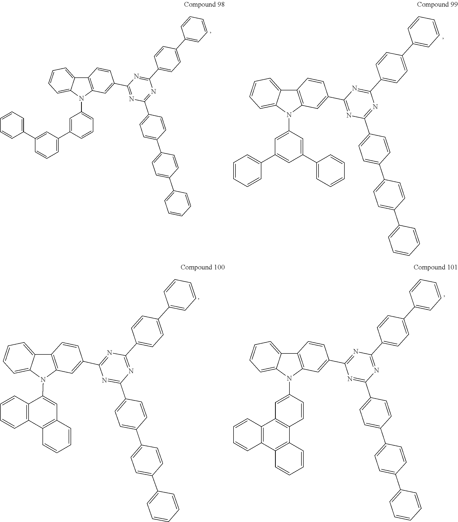
- the compound is selected from the group consisting of:
- an electroluminescent device which comprises:
- organic layer disposed between the anode and the cathode, wherein the organic layer comprising the compound having the structure of Formula 1:
- R a is selected from biphenyl, terphenyl, naphthyl, phenanthryl, triphenylene, fluorenyl, dibenzofuranyl;
- n is the number of R b , n is selected from 1, 2, 3 or 4; when n ⁇ 2, the R b is selected from the same or different structures; each of R b is independently selected from the group consisting of: hydrogen, deuterium, phenyl, biphenyl and terphenyl;
- R c , R d and R e are each independently selected from the group consisting of hydrogen, deuterium, halogen, a substituted or unsubstituted alkyl group having 1 to 20 carbon atoms, a substituted or unsubstituted cycloalkyl group having 3 to 20 ring carbon atoms, a substituted or unsubstituted heteroalkyl group having 1 to 20 carbon atoms, a substituted or unsubstituted arylalkyl group having 7 to 30 carbon atoms, a substituted or unsubstituted alkoxy group having 1 to 20 carbon atoms, a substituted or unsubstituted aryloxy group having 6 to 30 carbon atoms, a substituted or unsubstituted aryl group having 6 to 30 carbon atoms, a substituted or unsubstituted heteroaryl group having 3 to 30 carbon atoms, a substituted or unsubstituted alkylsilyl group having 3
- R 1 has the structure of Formula 2:
- L is selected from a single bond, or a substituted or unsubstituted arylene having 6 to 60 carbon atoms;
- R 2 and R 3 are each independently selected from the group consisting of hydrogen, deuterium, halogen, a substituted or unsubstituted alkyl group having 1 to 20 carbon atoms, a substituted or unsubstituted cycloalkyl group having 3 to 20 ring carbon atoms, a substituted or unsubstituted heteroalkyl group having 1 to 20 carbon atoms, a substituted or unsubstituted arylalkyl group having 7 to 30 carbon atoms, a substituted or unsubstituted alkoxy group having 1 to 20 carbon atoms, a substituted or unsubstituted aryloxy group having 6 to 30 carbon atoms, a substituted or unsubstituted aryl group having 6 to 30 carbon atoms, a substituted or unsubstituted alkylsilyl group having 3 to 20 carbon atoms, a substituted or unsubstituted arylsilyl group having 6 to 20 carbon
- R 2 and R 3 are selected from a substituted group in the group
- the substitution in the substituted group is selected from deuterium, halogen, an unsubstituted alkyl group having 1 to 20 carbon atoms, an unsubstituted cycloalkyl group having 3 to 20 ring carbon atoms, an unsubstituted heteroalkyl group having 1 to 20 carbon atoms, an unsubstituted arylalkyl group having 7 to 30 carbon atoms, an unsubstituted alkoxy group having 1 to 20 carbon atoms, an unsubstituted aryl group having 6 to 30 carbon atoms, and combinations thereof.
- the organic layer is a light emitting layer
- the compound is a host material
- the organic layer is a hole blocking layer
- the compound is a hole blocking material
- the light emitting layer further comprises at least one host material different from the compound having Formula 1.
- the light emitting layer further comprises phosphorescent material.
- the metal complex comprises at least one ligand
- the ligand comprises any one of the following structures:
- R x , R y , and R z can represent mono substitution, multiple substitutions or no substitution
- R x , R y , and R z are each independently selected from the group consisting of hydrogen, deuterium, halogen, a substituted or unsubstituted alkyl group having 1 to 20 carbon atoms, a substituted or unsubstituted cycloalkyl group having 3 to 20 ring carbon atoms, a substituted or unsubstituted heteroalkyl group having 1 to 20 carbon atoms, a substituted or unsubstituted arylalkyl group having 7 to 30 carbon atoms, a substituted or unsubstituted alkoxy group having 1 to 20 carbon atoms, a substituted or unsubstituted aryloxy group having 6 to 30 carbon atoms, a substituted or unsubstituted alkenyl group having 2 to 20 carbon atoms, a substituted or unsubstituted aryl group having 6 to 30 carbon atoms, a substituted or unsubstituted heteroaryl group having 3
- X b is selected from the group consisting of O, S, Se, NR N1 , CR C1 R C2 ;
- R N1 , R C1 and R C2 are each independently selected from the group consisting of hydrogen, deuterium, halogen, a substituted or unsubstituted alkyl group having 1 to 20 carbon atoms, a substituted or unsubstituted cycloalkyl group having 3 to 20 ring carbon atoms, a substituted or unsubstituted heteroalkyl group having 1 to 20 carbon atoms, a substituted or unsubstituted arylalkyl group having 7 to 30 carbon atoms, a substituted or unsubstituted alkoxy group having 1 to 20 carbon atoms, a substituted or unsubstituted aryloxy group having 6 to 30 carbon atoms, a substituted or unsubstituted alkenyl group having 2 to 20 carbon atoms, a substituted or unsubstituted aryl group having 6 to 30 carbon atoms, a substituted or unsubstituted heteroaryl group having 3 to 30
- a compound formulation comprising the compound represented by Formula 1 is further disclosed, the specific structure of the compound is described in any one of the embodiments aforementioned.
- the materials described in the present disclosure for a particular layer in an organic light emitting device may be used in combination with various other materials present in the device.
- the combinations of these materials are described in more detail in U.S. Pat. App. No. 20160359122A1 at paragraphs 0132-0161, which is incorporated by reference herein in its entirety.
- the materials described or referred to the disclosure are non-limiting examples of materials that may be useful in combination with the materials disclosed herein, and one of skill in the art may readily consult the literature to identify other materials that may be useful in combination.
- the materials described herein as useful for a particular layer in an organic light emitting device may be used in combination with a variety of other materials present in the device.
- the compounds disclosed herein may be used in combination with a wide variety of emitting dopants, hosts, transporting layers, blocking layers, injection layers, electrodes and other layers that may be present.
- the combination of these materials is described in detail in paragraphs 0080-0101 of U.S. Pat. App. No. 20150349273, which is incorporated by reference herein in its entirety.
- the materials described or referred to the disclosure are non-limiting examples of materials that may be useful in combination with the materials disclosed herein, and one of skill in the art may readily consult the literature to identify other materials that may be useful in combination.
- the characteristics of the device were also tested using conventional equipment in the art (including, but not limited to, evaporator produced by ANGSTROM ENGINEERING, optical testing system produced by SUZHOU FATAR, life testing system produced by SUZHOU FATAR, and ellipsometer produced by BEIJING ELLITOP, etc.) by methods well known to the persons skilled in the art.
- conventional equipment in the art including, but not limited to, evaporator produced by ANGSTROM ENGINEERING, optical testing system produced by SUZHOU FATAR, life testing system produced by SUZHOU FATAR, and ellipsometer produced by BEIJING ELLITOP, etc.
- the method for preparing the compound of the present invention is not limited.
- the following compounds are exemplified as a typical but non-limiting example, and the synthesis route and preparation method are as follows:
- 2-Bromo-carbazole (9.0 g, 36.57 mmol), 4-iodo-biphenyl (13.3 g, 47.54 mmol), CuCl (0.36 g, 3.66 mmol), 18-crown-6 (0.96 g, 3.66 mmol), 1,10-o-phenanthroline (0.66 g, 3.66 mmol), K 2 CO 3 (12.63 g, 91.43 mmol) were added to N-methyl pyrrolidone (200 mL) in a three-necked round-bottomed flask, protected by nitrogen, and heated to 180° C., reacted overnight.
- ITO indium tin oxide
- HIL hole injection layer
- HTL hole transporting layer
- EBL electron blocking layer
- the Compound GD was then doped in Compound H1 and Compound H2 be co-deposited as the emitting layer (EML).
- Compound 16 of the present disclosure was used as the hole blocking layer (HBL).
- HBL hole blocking layer
- Compound ET and 8-hydroxyquinolinolato-lithium (Liq) were co-deposition as an electron transporting layer (ETL).
- ETL electron transporting layer
- EIL electron injection layer
- Device Example 2 was fabricated in the same manner as in Device Example 1, except that using Compound 19 of the present disclosure instead of Compound 16 of the present disclosure as the hole blocking layer (HBL).
- HBL hole blocking layer
- Comparative Example 1 was fabricated in the same manner as in Device Example 1, except that using Compound H2 instead of Compound 16 of the present disclosure as the hole blocking layer (HBL).
- HBL hole blocking layer
- Comparative Example 2 was fabricated in the same manner as in Device Example 1, except that using Compound H3 instead of Compound 16 of the present disclosure as the hole blocking layer (HBL).
- HBL hole blocking layer
- Comparative Example 3 was fabricated in the same manner as in Device Example 1, except that using compound H4 instead of Compound 16 of the present disclosure as the hole blocking layer (HBL).
- HBL hole blocking layer
- Device Example 3 was fabricated in the same manner as in Comparative Example 1, except that using Compound 16 instead of Compound H2 in the emitting layer (EML).
- Comparative Example 4 was fabricated in the same manner as in Comparative Example 1, except that using the Compound H3 instead of Compound H2 in the emitting layer (EML).
- Comparative Example 5 was fabricated in the same manner as in Comparative Example 1, except that using the Compound H4 instead of Compound H2 in the emitting layer (EML).
- Device Examples 1-2 show the use of the material of the present disclosure in the hole blocking layer.
- the driving voltage of Device Example 1 was 2.78 V
- the power efficiency was 103 lm/W
- the maximum wavelength was 528 nm
- the CIE was 0.345, 0.627.
- the driving voltage of Example 2 was 2.81 V
- the power efficiency was 103 lm/W
- the maximum wavelength was 528 nm
- the CIE was 0.344, 0.628.
- the driving voltage of Comparative Example 1 was 2.94 V
- the power efficiency was 95 lm/W
- the maximum wavelength was 527 nm
- the CIE was 0.332 and 0.637.
- the driving voltage of Comparative Example 2 was 2.97 V, the power efficiency was 99 lm/W, the maximum wavelength was 528 nm, and the CIE was 0.344, 0.628.
- the driving voltage of Comparative Example 3 was 2.96 V, the power efficiency was 98 lm/W, the maximum wavelength was 528 nm, and the CIE was 0.342, 0.629.
- the above data shows that the emitting light of Device Examples 1-2 and Comparative Examples 1-3 are very close, but the power efficiency of Device Examples 1-2 are higher than that of Comparative Examples 1-3, and the driving voltage of Device Examples 1-2 are all lower than Examples 1-3. Especially in Device Example 1, the driving voltage is 2.78 V, which is very low.
- Device Example 3 shows the use of the material of the present invention as a host material in the light emitting layer.
- the test was performed at a constant current of 15 mA/cm 2 .
- the efficiency and driving voltage of Device Example 3 and Comparative Example 1 and Comparative Examples 4-5 were basically equivalent, but the lifetime of LT97 were respectively 335 h, 310 h, 222.6 h, and 254.5 h.
- the above data proves the structural characteristics of the compound of the present invention.
- the compound can be used as the hole blocking layer or a host material in the light-emitting layer by connecting a specific structure such as Formula 2 at a specific position of the carbazole ring in Formula 1, with specific selected substituents, which can improve the lifetime and efficiency of the device, reduce the driving voltage, and have important help to the industry.
Landscapes
- Chemical & Material Sciences (AREA)
- Organic Chemistry (AREA)
- Physics & Mathematics (AREA)
- Engineering & Computer Science (AREA)
- Materials Engineering (AREA)
- Spectroscopy & Molecular Physics (AREA)
- Electromagnetism (AREA)
- Electroluminescent Light Sources (AREA)
- Indole Compounds (AREA)
Abstract
Description

especially

The inventor of this application noticed various advantages of the compound obtained by combining carbazole with an aza six-membered aromatic ring such as pyridine, pyrimidine, and triazine, but it did not explicitly recognize the unique advantages of the triazine structure. In addition, in the choice of the position where the triazine is connected to the carbazole ring, it is not aware of the advantages of substitution positions on the carbazole ring other than the 3-position explicitly disclosed in this invention, especially the 2-position substitution.

those two compounds containing carbazole or phosphofluorene structural units. In this application, the advantages of introducing an aza-aromatic ring structure on the carbazole ring are noted, but the position of introducing an aza-aromatic ring is variable, involving the 2-, 3- and 9-positions (on the nitrogen atom of carbazole) substituted compounds, and it does not realize the special advantage of fixing the triazine group at a specific position of the carbazole ring for substitution.


| TABLE 1 |
| Device Structure |
| Device ID | HIL | HTL | EBL | EML | HBL | ETL |
| Device | Compound | Compound | Compound | Compound | Compound | Compound |
| Example 1 | HI (100 Å) | HT (350 Å) | H1 (50 Å) | H1:Compound | 16 (100 Å) | ET:Liq |
| H2:Compound GD | (40:60) | |||||
| (45:45:10) | (350 Å) | |||||
| (400 Å) | ||||||
| Device | Compound | Compound | Compound | Compound | Compound | Compound |
| Example 2 | HI (100 Å) | HT (350 Å) | H1 (50 Å) | H1:Compound | 19 (100 Å) | ET:Liq |
| H2:Compound GD | (40:60) | |||||
| (45:45:10) | (350 Å) | |||||
| (400 Å) | ||||||
| Comparative | Compound | Compound | Compound | Compound | Compound | Compound |
| Example 1 | HI (100 Å) | HT (350 Å) | H1 (50 Å) | H1:Compound | H2 (100 Å) | ET:Liq |
| H2:Compound GD | (40:60) | |||||
| (45:45:10) | (350 Å) | |||||
| (400 Å) | ||||||
| Comparative | Compound | Compound | Compound | Compound | Compound | Compound |
| Example 2 | HI (100 Å) | HT (350 Å) | H1 (50 Å) | H1:Compound | H3 (100 Å) | ET:Liq |
| H2:Compound GD | (40:60) | |||||
| (45:45:10) | (350 Å) | |||||
| (400 Å) | ||||||
| Comparative | Compound | Compound | Compound | Compound | Compound | Compound |
| Example 3 | HI | HT (350 Å) | H1 (50 Å) | H1:Compound | H4 (100 Å) | ET:Liq |
| (100 Å) | H2:Compound GD | (40:60) | ||||
| (45:45:10) | (350 Å) | |||||
| (400 Å) | ||||||
| Device | Compound | Compound | Compound | Compound | Compound | Compound |
| Example 3 | HI (100 Å) | HT (350 Å) | H1 (50 Å) | H1:Compound | H2 (100 Å) | ET:Liq |
| 16:Compound GD | (40:60) | |||||
| (45:45:10) | (350 Å) | |||||
| (400 Å) | ||||||
| Comparative | Compound | Compound | Compound | Compound | Compound | Compound |
| Example 4 | HI (100 Å) | HT (350 Å) | H1 (50 Å) | H1:Compound | H2 (100 Å) | ET:Liq |
| H3:Compound GD | (40:60) | |||||
| (45:45:10) | (350 Å) | |||||
| (400 Å) | ||||||
| Comparative | Compound | Compound | Compound | Compound | Compound | Compound |
| Example 5 | HI (100 Å) | HT (350 Å) | H1 (50 Å) | H1:Compound | H2 (100 Å) | ET: Liq |
| H4:Compound GD | (40:60) | |||||
| (45:45:10) | (350 Å) | |||||
| (400 Å) | ||||||

Claims (14)


Applications Claiming Priority (2)
| Application Number | Priority Date | Filing Date | Title |
|---|---|---|---|
| CN201910149767.3A CN111620853B (en) | 2019-02-28 | 2019-02-28 | Organic electroluminescent material and device thereof |
| CN201910149767.3 | 2019-02-28 |
Publications (2)
| Publication Number | Publication Date |
|---|---|
| US20200277283A1 US20200277283A1 (en) | 2020-09-03 |
| US11708356B2 true US11708356B2 (en) | 2023-07-25 |
Family
ID=72236015
Family Applications (1)
| Application Number | Title | Priority Date | Filing Date |
|---|---|---|---|
| US16/803,280 Active 2041-04-05 US11708356B2 (en) | 2019-02-28 | 2020-02-27 | Organic electroluminescent materials and devices |
Country Status (2)
| Country | Link |
|---|---|
| US (1) | US11708356B2 (en) |
| CN (1) | CN111620853B (en) |
Cited By (1)
| Publication number | Priority date | Publication date | Assignee | Title |
|---|---|---|---|---|
| US20240038096A1 (en) * | 2022-07-26 | 2024-02-01 | Triad National Security, Llc | Method and system for simulating handling of radioactive material safety during training |
Families Citing this family (7)
| Publication number | Priority date | Publication date | Assignee | Title |
|---|---|---|---|---|
| KR20220043506A (en) * | 2020-09-29 | 2022-04-05 | 엘티소재주식회사 | Heterocyclic compound and organic light emitting device including the same |
| CN113387939A (en) * | 2021-06-30 | 2021-09-14 | 南京高光半导体材料有限公司 | Compound containing carbazole and carbazole derivatives and organic electroluminescent device |
| CN114075181B (en) * | 2021-08-31 | 2024-02-02 | 陕西莱特迈思光电材料有限公司 | Nitrogen-containing compound, and organic electroluminescent device and electronic device using same |
| CN114075182B (en) * | 2021-09-23 | 2023-10-31 | 陕西莱特迈思光电材料有限公司 | Nitrogen-containing compound, organic electroluminescent device using same and electronic device |
| CN116156912A (en) * | 2021-11-20 | 2023-05-23 | 北京夏禾科技有限公司 | An organic electroluminescent device |
| KR102564921B1 (en) * | 2022-02-04 | 2023-08-09 | 엘티소재주식회사 | Heterocyclic compound, organic light emitting device comprising the same and composition for organic layer of organic light emitting device |
| CN114907322B (en) * | 2022-05-09 | 2024-05-03 | 吉林奥来德光电材料股份有限公司 | Electronic transmission material containing heterocyclic structure and preparation method and application thereof |
Citations (33)
| Publication number | Priority date | Publication date | Assignee | Title |
|---|---|---|---|---|
| US5703436A (en) | 1994-12-13 | 1997-12-30 | The Trustees Of Princeton University | Transparent contacts for organic devices |
| US5707745A (en) | 1994-12-13 | 1998-01-13 | The Trustees Of Princeton University | Multicolor organic light emitting devices |
| US5844363A (en) | 1997-01-23 | 1998-12-01 | The Trustees Of Princeton Univ. | Vacuum deposited, non-polymeric flexible organic light emitting devices |
| US6097147A (en) | 1998-09-14 | 2000-08-01 | The Trustees Of Princeton University | Structure for high efficiency electroluminescent device |
| US6303238B1 (en) | 1997-12-01 | 2001-10-16 | The Trustees Of Princeton University | OLEDs doped with phosphorescent compounds |
| US20030230980A1 (en) | 2002-06-18 | 2003-12-18 | Forrest Stephen R | Very low voltage, high efficiency phosphorescent oled in a p-i-n structure |
| US20040067387A1 (en) * | 2002-05-07 | 2004-04-08 | Ji-Eun Kim | Organic compounds for electroluminescence and organic electroluminescent devices using the same |
| US20040174116A1 (en) | 2001-08-20 | 2004-09-09 | Lu Min-Hao Michael | Transparent electrodes |
| US7279704B2 (en) | 2004-05-18 | 2007-10-09 | The University Of Southern California | Complexes with tridentate ligands |
| US7968146B2 (en) | 2006-11-01 | 2011-06-28 | The Trustees Of Princeton University | Hybrid layers for use in coatings on electronic devices or other articles |
| US20120223276A1 (en) | 2009-11-14 | 2012-09-06 | Merck Patent Gmbh | Materials for electronic devices |
| WO2013100538A1 (en) | 2011-12-26 | 2013-07-04 | 제일모직 주식회사 | Compound for organic optoelectric device, organic light emitting element including same, and display device including said organic light emitting element |
| US20140131665A1 (en) | 2012-11-12 | 2014-05-15 | Universal Display Corporation | Organic Electroluminescent Device With Delayed Fluorescence |
| US20140158992A1 (en) | 2012-12-07 | 2014-06-12 | Universal Display Corporation | Carbazole Compounds For Delayed Fluorescence |
| US20150001471A1 (en) | 2013-06-28 | 2015-01-01 | Universal Display Corporation | Novel host materials for pholeds |
| US20150053939A1 (en) | 2013-08-20 | 2015-02-26 | Universal Display Corporation | Organic electroluminescent materials and devices |
| US20150228908A1 (en) | 2014-02-11 | 2015-08-13 | Samsung Electronics Co., Ltd. | Carbazole-based compound and organic light-emitting device including the same |
| US20150243903A1 (en) | 2014-02-27 | 2015-08-27 | Universal Display Corporation | Organic electroluminescent materials and devices |
| US20150349273A1 (en) | 2014-06-03 | 2015-12-03 | Universal Display Corporation | Organic electroluminescent materials and devices |
| US20160028021A1 (en) | 2014-07-09 | 2016-01-28 | Universal Display Corporation | Organic electroluminescent materials and devices |
| EP2991128A1 (en) | 2014-08-29 | 2016-03-02 | Samsung Electronics Co., Ltd. | Organic light-emitting device |
| US20160093808A1 (en) | 2014-09-29 | 2016-03-31 | Universal Display Corporation | Organic electroluminescent materials and devices |
| US20160359122A1 (en) | 2015-06-04 | 2016-12-08 | Universal Display Corporation | Organic electroluminescent materials and devices |
| US20170025618A1 (en) | 2015-04-06 | 2017-01-26 | Universal Display Corporation | Organic Electroluminescent Materials and Devices |
| US20170054087A1 (en) | 2015-08-17 | 2017-02-23 | Universal Display Corporation | Organic electroluminescent materials and devices |
| CN107188886A (en) | 2016-03-15 | 2017-09-22 | 上海和辉光电有限公司 | A kind of organic electroluminescent compounds and the OLED containing the compound |
| WO2018021854A1 (en) * | 2016-07-27 | 2018-02-01 | 주식회사 엘지화학 | Polycyclic compound and organic light-emitting element comprising same |
| KR20180060474A (en) | 2016-11-29 | 2018-06-07 | 희성소재 (주) | Hetero-cyclic compound and organic light emitting device using the same |
| WO2018103745A1 (en) * | 2016-12-08 | 2018-06-14 | 广州华睿光电材料有限公司 | Carbazole compound and use thereof |
| US20180166634A1 (en) | 2016-12-14 | 2018-06-14 | Samsung Electronics Co., Ltd. | Organic light-emitting device and compound |
| US20180301639A1 (en) | 2015-04-06 | 2018-10-18 | Universal Display Corporation | Organic electroluminescent materials and devices |
| CN108727358A (en) | 2018-08-06 | 2018-11-02 | 长春海谱润斯科技有限公司 | A kind of heterocyclic compound and its organic electroluminescence device |
| WO2019190230A1 (en) * | 2018-03-28 | 2019-10-03 | 주식회사 엘지화학 | Compound and organic light emitting diode comprising same |
-
2019
- 2019-02-28 CN CN201910149767.3A patent/CN111620853B/en active Active
-
2020
- 2020-02-27 US US16/803,280 patent/US11708356B2/en active Active
Patent Citations (34)
| Publication number | Priority date | Publication date | Assignee | Title |
|---|---|---|---|---|
| US5703436A (en) | 1994-12-13 | 1997-12-30 | The Trustees Of Princeton University | Transparent contacts for organic devices |
| US5707745A (en) | 1994-12-13 | 1998-01-13 | The Trustees Of Princeton University | Multicolor organic light emitting devices |
| US5844363A (en) | 1997-01-23 | 1998-12-01 | The Trustees Of Princeton Univ. | Vacuum deposited, non-polymeric flexible organic light emitting devices |
| US6303238B1 (en) | 1997-12-01 | 2001-10-16 | The Trustees Of Princeton University | OLEDs doped with phosphorescent compounds |
| US6097147A (en) | 1998-09-14 | 2000-08-01 | The Trustees Of Princeton University | Structure for high efficiency electroluminescent device |
| US20040174116A1 (en) | 2001-08-20 | 2004-09-09 | Lu Min-Hao Michael | Transparent electrodes |
| US20040067387A1 (en) * | 2002-05-07 | 2004-04-08 | Ji-Eun Kim | Organic compounds for electroluminescence and organic electroluminescent devices using the same |
| US20030230980A1 (en) | 2002-06-18 | 2003-12-18 | Forrest Stephen R | Very low voltage, high efficiency phosphorescent oled in a p-i-n structure |
| US7279704B2 (en) | 2004-05-18 | 2007-10-09 | The University Of Southern California | Complexes with tridentate ligands |
| US7968146B2 (en) | 2006-11-01 | 2011-06-28 | The Trustees Of Princeton University | Hybrid layers for use in coatings on electronic devices or other articles |
| US20120223276A1 (en) | 2009-11-14 | 2012-09-06 | Merck Patent Gmbh | Materials for electronic devices |
| WO2013100538A1 (en) | 2011-12-26 | 2013-07-04 | 제일모직 주식회사 | Compound for organic optoelectric device, organic light emitting element including same, and display device including said organic light emitting element |
| US20140131665A1 (en) | 2012-11-12 | 2014-05-15 | Universal Display Corporation | Organic Electroluminescent Device With Delayed Fluorescence |
| US20140158992A1 (en) | 2012-12-07 | 2014-06-12 | Universal Display Corporation | Carbazole Compounds For Delayed Fluorescence |
| US20150001471A1 (en) | 2013-06-28 | 2015-01-01 | Universal Display Corporation | Novel host materials for pholeds |
| US20150053939A1 (en) | 2013-08-20 | 2015-02-26 | Universal Display Corporation | Organic electroluminescent materials and devices |
| US20150228908A1 (en) | 2014-02-11 | 2015-08-13 | Samsung Electronics Co., Ltd. | Carbazole-based compound and organic light-emitting device including the same |
| US20150243903A1 (en) | 2014-02-27 | 2015-08-27 | Universal Display Corporation | Organic electroluminescent materials and devices |
| US20150349273A1 (en) | 2014-06-03 | 2015-12-03 | Universal Display Corporation | Organic electroluminescent materials and devices |
| US20160028021A1 (en) | 2014-07-09 | 2016-01-28 | Universal Display Corporation | Organic electroluminescent materials and devices |
| EP2991128A1 (en) | 2014-08-29 | 2016-03-02 | Samsung Electronics Co., Ltd. | Organic light-emitting device |
| US20160093808A1 (en) | 2014-09-29 | 2016-03-31 | Universal Display Corporation | Organic electroluminescent materials and devices |
| US20180301639A1 (en) | 2015-04-06 | 2018-10-18 | Universal Display Corporation | Organic electroluminescent materials and devices |
| US20170025618A1 (en) | 2015-04-06 | 2017-01-26 | Universal Display Corporation | Organic Electroluminescent Materials and Devices |
| US20160359122A1 (en) | 2015-06-04 | 2016-12-08 | Universal Display Corporation | Organic electroluminescent materials and devices |
| US20170054087A1 (en) | 2015-08-17 | 2017-02-23 | Universal Display Corporation | Organic electroluminescent materials and devices |
| CN107188886A (en) | 2016-03-15 | 2017-09-22 | 上海和辉光电有限公司 | A kind of organic electroluminescent compounds and the OLED containing the compound |
| WO2018021854A1 (en) * | 2016-07-27 | 2018-02-01 | 주식회사 엘지화학 | Polycyclic compound and organic light-emitting element comprising same |
| US20190237674A1 (en) * | 2016-07-27 | 2019-08-01 | Lg Chem Ltd. | Multicyclic compound and organic light emitting device including the same (as amended) |
| KR20180060474A (en) | 2016-11-29 | 2018-06-07 | 희성소재 (주) | Hetero-cyclic compound and organic light emitting device using the same |
| WO2018103745A1 (en) * | 2016-12-08 | 2018-06-14 | 广州华睿光电材料有限公司 | Carbazole compound and use thereof |
| US20180166634A1 (en) | 2016-12-14 | 2018-06-14 | Samsung Electronics Co., Ltd. | Organic light-emitting device and compound |
| WO2019190230A1 (en) * | 2018-03-28 | 2019-10-03 | 주식회사 엘지화학 | Compound and organic light emitting diode comprising same |
| CN108727358A (en) | 2018-08-06 | 2018-11-02 | 长春海谱润斯科技有限公司 | A kind of heterocyclic compound and its organic electroluminescence device |
Non-Patent Citations (5)
| Title |
|---|
| Chinese First Office Action, for Chinese Application No. 201910149767.3 and its English translation, dated April 20, 2022. |
| Joyama et al., "Highly efficient organic light-emitting diodes from delayed fluorescence", Nature; vol. 492, pp. 234-238 (2012). |
| Machine English translation of Jang et al. (WO 2019/190230 A1). Apr. 25, 2022. * |
| Machine English translation of Pan et al. (WO 2018/103745 A1). Apr. 25, 2022. * |
| Tang et al., "Organic electroluminescent diodes", Applied Physics Letters, 51(12): 913-915 (1987). |
Cited By (1)
| Publication number | Priority date | Publication date | Assignee | Title |
|---|---|---|---|---|
| US20240038096A1 (en) * | 2022-07-26 | 2024-02-01 | Triad National Security, Llc | Method and system for simulating handling of radioactive material safety during training |
Also Published As
| Publication number | Publication date |
|---|---|
| US20200277283A1 (en) | 2020-09-03 |
| CN111620853A (en) | 2020-09-04 |
| CN111620853B (en) | 2023-07-28 |
Similar Documents
| Publication | Publication Date | Title |
|---|---|---|
| US20250072279A1 (en) | Metal complex with fluorine substitution | |
| US12156466B2 (en) | Organic electroluminescent material and device | |
| US11329237B2 (en) | Boron and nitrogen containing heterocyclic compounds | |
| US10998506B2 (en) | Boron containing heterocyclic compound for OLEDs, an organic light-emitting device, and a formulation comprising the boron-containing heterocyclic compound | |
| US20200099000A1 (en) | Organic luminescent materials containing novel ancillary ligands | |
| US11839147B2 (en) | Hole injection layer and charge generation layer containing a truxene based compound | |
| US12557543B2 (en) | Light-emitting material with a polycyclic ligand | |
| US20190194234A1 (en) | Metal complexes containing heterocycle substituted ligands, and electroluminescent devices and formulations containing the complexes | |
| US11708356B2 (en) | Organic electroluminescent materials and devices | |
| US11498937B2 (en) | Organic luminescent material including 3-deuterium-substituted isoquinoline ligand | |
| US11581498B2 (en) | Organic luminescent material containing 6-silyl-substituted isoquinoline ligand | |
| US11201290B2 (en) | Tetraphenylene anthracene compounds | |
| US10978645B2 (en) | Indolocarbazole tetraphenylene compounds | |
| US11653559B2 (en) | Metal complex containing a first ligand, a second ligand, and a third ligand | |
| US20190077818A1 (en) | Organic luminescent materials containing fluorine ancillary ligands | |
| US12389790B2 (en) | Organic electroluminescent material and device | |
| US11512038B2 (en) | Tetraphenylene triarylamine compounds | |
| US12398150B2 (en) | Organic electroluminescent material and device thereof | |
| US10957869B2 (en) | Organic luminescent materials containing cycloalkyl ancillary ligands | |
| US12201014B2 (en) | Metal complex, electroluminescent device including the same, and use thereof | |
| US11325934B2 (en) | Organic luminescent materials containing tetraphenylene ligands | |
| US20190165278A1 (en) | Thiophene-containing triarylamine compounds | |
| US20190109284A1 (en) | Crosslinkable deuterated charge transporting compound, an organic electroluminescent device comprising the compound, and a solution formulation | |
| US20220194956A1 (en) | Organic electroluminescent material and device thereof | |
| US12289984B2 (en) | Metal complex containing azabenzothiazole |
Legal Events
| Date | Code | Title | Description |
|---|---|---|---|
| AS | Assignment |
Owner name: BEIJING SUMMER SPROUT TECHNOLOGY CO., LTD., CHINA Free format text: ASSIGNMENT OF ASSIGNORS INTEREST;ASSIGNORS:LI, FENG;WANG, LE;LI, CHANGQING;AND OTHERS;SIGNING DATES FROM 20200220 TO 20200226;REEL/FRAME:051953/0381 |
|
| FEPP | Fee payment procedure |
Free format text: ENTITY STATUS SET TO UNDISCOUNTED (ORIGINAL EVENT CODE: BIG.); ENTITY STATUS OF PATENT OWNER: SMALL ENTITY |
|
| FEPP | Fee payment procedure |
Free format text: ENTITY STATUS SET TO SMALL (ORIGINAL EVENT CODE: SMAL); ENTITY STATUS OF PATENT OWNER: SMALL ENTITY |
|
| STPP | Information on status: patent application and granting procedure in general |
Free format text: DOCKETED NEW CASE - READY FOR EXAMINATION |
|
| STPP | Information on status: patent application and granting procedure in general |
Free format text: NON FINAL ACTION MAILED |
|
| STPP | Information on status: patent application and granting procedure in general |
Free format text: RESPONSE TO NON-FINAL OFFICE ACTION ENTERED AND FORWARDED TO EXAMINER |
|
| STPP | Information on status: patent application and granting procedure in general |
Free format text: FINAL REJECTION MAILED |
|
| STPP | Information on status: patent application and granting procedure in general |
Free format text: DOCKETED NEW CASE - READY FOR EXAMINATION |
|
| STPP | Information on status: patent application and granting procedure in general |
Free format text: NON FINAL ACTION MAILED |
|
| STPP | Information on status: patent application and granting procedure in general |
Free format text: PUBLICATIONS -- ISSUE FEE PAYMENT VERIFIED |
|
| STCF | Information on status: patent grant |
Free format text: PATENTED CASE |