US11509400B2 - Image transmission system and image transmission method - Google Patents
Image transmission system and image transmission method Download PDFInfo
- Publication number
- US11509400B2 US11509400B2 US17/096,973 US202017096973A US11509400B2 US 11509400 B2 US11509400 B2 US 11509400B2 US 202017096973 A US202017096973 A US 202017096973A US 11509400 B2 US11509400 B2 US 11509400B2
- Authority
- US
- United States
- Prior art keywords
- image
- transmission system
- printed circuit
- flexible printed
- image transmission
- Prior art date
- Legal status (The legal status is an assumption and is not a legal conclusion. Google has not performed a legal analysis and makes no representation as to the accuracy of the status listed.)
- Active, expires
Links
Images


Classifications
-
- H—ELECTRICITY
- H04—ELECTRIC COMMUNICATION TECHNIQUE
- H04N—PICTORIAL COMMUNICATION, e.g. TELEVISION
- H04N23/00—Cameras or camera modules comprising electronic image sensors; Control thereof
- H04N23/90—Arrangement of cameras or camera modules, e.g. multiple cameras in TV studios or sports stadiums
-
- H—ELECTRICITY
- H04—ELECTRIC COMMUNICATION TECHNIQUE
- H04B—TRANSMISSION
- H04B10/00—Transmission systems employing electromagnetic waves other than radio-waves, e.g. infrared, visible or ultraviolet light, or employing corpuscular radiation, e.g. quantum communication
- H04B10/80—Optical aspects relating to the use of optical transmission for specific applications, not provided for in groups H04B10/03 - H04B10/70, e.g. optical power feeding or optical transmission through water
- H04B10/801—Optical aspects relating to the use of optical transmission for specific applications, not provided for in groups H04B10/03 - H04B10/70, e.g. optical power feeding or optical transmission through water using optical interconnects, e.g. light coupled isolators, circuit board interconnections
-
- H—ELECTRICITY
- H05—ELECTRIC TECHNIQUES NOT OTHERWISE PROVIDED FOR
- H05K—PRINTED CIRCUITS; CASINGS OR CONSTRUCTIONAL DETAILS OF ELECTRIC APPARATUS; MANUFACTURE OF ASSEMBLAGES OF ELECTRICAL COMPONENTS
- H05K1/00—Printed circuits
- H05K1/18—Printed circuits structurally associated with non-printed electric components
- H05K1/189—Printed circuits structurally associated with non-printed electric components characterised by the use of a flexible or folded printed circuit
-
- G—PHYSICS
- G02—OPTICS
- G02B—OPTICAL ELEMENTS, SYSTEMS OR APPARATUS
- G02B6/00—Light guides; Structural details of arrangements comprising light guides and other optical elements, e.g. couplings
- G02B6/10—Light guides; Structural details of arrangements comprising light guides and other optical elements, e.g. couplings of the optical waveguide type
- G02B6/12—Light guides; Structural details of arrangements comprising light guides and other optical elements, e.g. couplings of the optical waveguide type of the integrated circuit kind
- G02B6/12004—Combinations of two or more optical elements
-
- H—ELECTRICITY
- H04—ELECTRIC COMMUNICATION TECHNIQUE
- H04B—TRANSMISSION
- H04B10/00—Transmission systems employing electromagnetic waves other than radio-waves, e.g. infrared, visible or ultraviolet light, or employing corpuscular radiation, e.g. quantum communication
- H04B10/80—Optical aspects relating to the use of optical transmission for specific applications, not provided for in groups H04B10/03 - H04B10/70, e.g. optical power feeding or optical transmission through water
-
- H—ELECTRICITY
- H04—ELECTRIC COMMUNICATION TECHNIQUE
- H04N—PICTORIAL COMMUNICATION, e.g. TELEVISION
- H04N23/00—Cameras or camera modules comprising electronic image sensors; Control thereof
- H04N23/57—Mechanical or electrical details of cameras or camera modules specially adapted for being embedded in other devices
-
- H—ELECTRICITY
- H04—ELECTRIC COMMUNICATION TECHNIQUE
- H04N—PICTORIAL COMMUNICATION, e.g. TELEVISION
- H04N5/00—Details of television systems
- H04N5/66—Transforming electric information into light information
-
- H—ELECTRICITY
- H05—ELECTRIC TECHNIQUES NOT OTHERWISE PROVIDED FOR
- H05K—PRINTED CIRCUITS; CASINGS OR CONSTRUCTIONAL DETAILS OF ELECTRIC APPARATUS; MANUFACTURE OF ASSEMBLAGES OF ELECTRICAL COMPONENTS
- H05K1/00—Printed circuits
- H05K1/02—Details
- H05K1/0274—Optical details, e.g. printed circuits comprising integral optical means
-
- H—ELECTRICITY
- H05—ELECTRIC TECHNIQUES NOT OTHERWISE PROVIDED FOR
- H05K—PRINTED CIRCUITS; CASINGS OR CONSTRUCTIONAL DETAILS OF ELECTRIC APPARATUS; MANUFACTURE OF ASSEMBLAGES OF ELECTRICAL COMPONENTS
- H05K1/00—Printed circuits
- H05K1/02—Details
- H05K1/14—Structural association of two or more printed circuits
- H05K1/147—Structural association of two or more printed circuits at least one of the printed circuits being bent or folded, e.g. by using a flexible printed circuit
-
- H—ELECTRICITY
- H05—ELECTRIC TECHNIQUES NOT OTHERWISE PROVIDED FOR
- H05K—PRINTED CIRCUITS; CASINGS OR CONSTRUCTIONAL DETAILS OF ELECTRIC APPARATUS; MANUFACTURE OF ASSEMBLAGES OF ELECTRICAL COMPONENTS
- H05K2201/00—Indexing scheme relating to printed circuits covered by H05K1/00
- H05K2201/05—Flexible printed circuits [FPCs]
- H05K2201/052—Branched
-
- H—ELECTRICITY
- H05—ELECTRIC TECHNIQUES NOT OTHERWISE PROVIDED FOR
- H05K—PRINTED CIRCUITS; CASINGS OR CONSTRUCTIONAL DETAILS OF ELECTRIC APPARATUS; MANUFACTURE OF ASSEMBLAGES OF ELECTRICAL COMPONENTS
- H05K2201/00—Indexing scheme relating to printed circuits covered by H05K1/00
- H05K2201/10—Details of components or other objects attached to or integrated in a printed circuit board
- H05K2201/10007—Types of components
- H05K2201/10121—Optical component, e.g. opto-electronic component
-
- H—ELECTRICITY
- H05—ELECTRIC TECHNIQUES NOT OTHERWISE PROVIDED FOR
- H05K—PRINTED CIRCUITS; CASINGS OR CONSTRUCTIONAL DETAILS OF ELECTRIC APPARATUS; MANUFACTURE OF ASSEMBLAGES OF ELECTRICAL COMPONENTS
- H05K2201/00—Indexing scheme relating to printed circuits covered by H05K1/00
- H05K2201/10—Details of components or other objects attached to or integrated in a printed circuit board
- H05K2201/10007—Types of components
- H05K2201/10151—Sensor
-
- H—ELECTRICITY
- H05—ELECTRIC TECHNIQUES NOT OTHERWISE PROVIDED FOR
- H05K—PRINTED CIRCUITS; CASINGS OR CONSTRUCTIONAL DETAILS OF ELECTRIC APPARATUS; MANUFACTURE OF ASSEMBLAGES OF ELECTRICAL COMPONENTS
- H05K2201/00—Indexing scheme relating to printed circuits covered by H05K1/00
- H05K2201/20—Details of printed circuits not provided for in H05K2201/01 - H05K2201/10
- H05K2201/2009—Reinforced areas, e.g. for a specific part of a flexible printed circuit
Definitions
- the present disclosure relates to a transmission system and a transmission method. More particularly, the present disclosure relates to an image transmission system for transmitting data through a flexible printed circuit (FPC), and an image data transmission method.
- FPC flexible printed circuit
- RF Radio frequency
- the RF function can be, for example, Wi-Fi, blue tooth, WLAN (Wireless Local Area Networks) . . . etc. Therefore, demand for data transmission and data computing of portable devices grows with each passing day.
- the present disclosure provides an image transmission system.
- the image transmission system includes at least one image capturing device, at least one conversion device, at least one image processor, and at least one flexible printed circuit (FPC).
- the at least one FPC includes at least one conductive layer and at least one optical waveguide layer.
- the at least one image capturing device is configured to capture at least one data.
- the at least one conversion device is configured to perform a conversion between the at least one data and an optical signal.
- the at least one image processor is configured to obtain the at least one data according to the optical signal, and processes the data.
- the at least one optical waveguide layer is configured to transmit the optical signal.
- the present disclosure provides an image transmission system.
- the image transmission system includes a plurality of image capturing devices, at least one serializing/deserializing circuit, at least one conversion device, at least one image processor, and at least one flexible printed circuit.
- the image capturing devices is configured to capture a plurality of data.
- the at least one serializing/deserializing circuit is configured to perform a conversion between the data and a serial data.
- the at least one conversion device is configured to perform a conversion between the serial data and an optical signal.
- the at least one image processor is configured to obtain the data according to the optical signal, and process the data.
- the at least one flexible printed circuit includes at least one conductive layer and at least one optical waveguide layer.
- the at least one optical waveguide layer is configured to transmit the optical signal.
- An image transmission method includes steps of: a data is converted into a serial data through a serializing/deserializing circuit; subsequently, the serial data is converted into an optical signal; and transmitting the optical signal through an optical waveguide layer of a flexible printed circuit.
- the image transmission system and the image transmission method of the present disclosure adopt a flexible printed circuit to transmit signals with high speed.
- the image transmission system of the present disclosure adopts serializing/deserializing circuit. Therefore, the numbers of pins of the image transmission system of the present disclosure can be reduced efficiently, so as to decrease numbers of transmission lines and interference, such that an excellent solution for image transmission with high speed is provided.
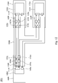
- FIG. 1 depicts a schematic diagram of an image transmission system according to one embodiment of the present disclosure
- FIG. 2 depicts a schematic diagram of a cross-sectional view of the image transmission system shown in FIG. 1 according to one embodiment of the present disclosure
- FIG. 3 depicts a schematic diagram of an image transmission system according to one embodiment of the present disclosure
- FIG. 4 depicts a schematic diagram of a cross-sectional view of the image transmission system shown in FIG. 3 according to one embodiment of the present disclosure
- FIG. 5 depicts a schematic diagram of an image transmission system according to one embodiment of the present disclosure
- FIG. 6 depicts a schematic diagram of a cross-sectional view of the image transmission system shown in FIG. 5 according to one embodiment of the present disclosure
- FIG. 7 depicts a schematic diagram of an image transmission system according to one embodiment of the present disclosure.
- FIG. 8 depicts a schematic diagram of an image transmission system according to one embodiment of the present disclosure.
- FIG. 9 depicts a schematic diagram of an image transmission system according to one embodiment of the present disclosure.
- FIG. 10 depicts a schematic diagram of an image transmission system according to one embodiment of the present disclosure.
- FIG. 11 depicts a schematic diagram of an image transmission system according to one embodiment of the present disclosure.
- FIG. 12 depicts a schematic diagram of an image transmission system according to one embodiment of the present disclosure.
- FIG. 13 depicts a schematic diagram of an image transmission system according to one embodiment of the present disclosure.
- FIG. 14 depicts a schematic diagram of a cross-sectional view of the image transmission system shown in FIG. 13 according to one embodiment of the present disclosure
- FIG. 15 depicts a schematic diagram of an image transmission system according to one embodiment of the present disclosure.
- FIG. 16 depicts a schematic diagram of a cross-sectional view of the image transmission system shown in FIG. 15 according to one embodiment of the present disclosure
- FIG. 17 depicts a schematic diagram of an image transmission system according to one embodiment of the present disclosure.
- FIG. 18 depicts a schematic diagram of a cross-sectional view of the image transmission system shown in FIG. 17 according to one embodiment of the present disclosure
- FIG. 19 depicts a schematic diagram of an image transmission system according to one embodiment of the present disclosure.
- FIG. 20 depicts a schematic diagram of a cross-sectional view of the image transmission system shown in FIG. 19 according to one embodiment of the present disclosure
- FIG. 21 depicts a schematic diagram of an image transmission system according to one embodiment of the present disclosure.
- FIG. 22 depicts a schematic diagram of an image transmission system according to one embodiment of the present disclosure.
- FIG. 23 depicts a schematic diagram of an image transmission system according to one embodiment of the present disclosure.
- FIG. 24 depicts a flowchart of an image transmission method according to one embodiment of the present disclosure.
- FIG. 1 depicts a schematic diagram of an image transmission system 100 according to one embodiment of the present disclosure.
- the image transmission system 100 includes an image capturing device 110 , a conversion device 120 , a flexible printed circuit 130 , an image processor 140 , and a conversion device 150 .
- FIG. 2 depicts a schematic diagram of a cross-sectional view along line AA′ of the image transmission system 100 shown in FIG. 1 according to one embodiment of the present disclosure.
- the flexible printed circuit 130 includes a conductive layer 131 and an optical waveguide layer 133 .
- the image capturing device 110 captures data, transmits it to the conversion device 120 , and the conversion device 120 converts the data into an optical signal 134 . Subsequently, the conversion device 120 transmits the optical signal 134 to the optical waveguide layer 133 , and the optical waveguide layer 133 transmits the optical signal 134 . Then, the conversion device 150 receives the optical signal 134 , converts it into the data, and transmits the data to the image processor 140 , such that the image processor 140 may perform an image data processing to the data.
- the image transmission system 100 of the present disclosure adopts the optical signal 134 to transmit data through the optical waveguide layer 133 of the flexible printed circuit 130 . Therefore, the image transmission speed or the image transmission capacity of the image transmission system 100 of the present disclosure is increased substantially. As a result, complex data can be quickly transmitted to the image processor 140 through the optical waveguide layer 133 of the flexible printed circuit 130 , such that the image processor 140 may perform an image data processing to the data, so as to improve the entire transmission and processing speed of the data. If the image transmission system 100 is introduced in electronical products, it may bring a fast/quick response experience to users.
- the flexible printed circuit 130 can be a highly integrated OE-FPC (Optoelectronics Flexible Printed Circuit).
- OE-FPC can transmit electrical signals for controlling electrical elements, and transmit optical signals 134 including carrier waves for carrying data.
- the electrical signals can be transmitted to the conductive layer 131 through an input/output interface 113 of the image capturing device 110 , and the conductive layer 131 transmits it to an input/output interface 143 of the image processor 140 .
- the electrical signals can be voltage control instructions (e.g., a DC voltage with 0.5V is regard as a voltage control instruction) or electrical control instructions carried by carrier waves (e.g., control instructions in connection with electricity, which are carried by AC carrier waves).
- the data can be image data, electrical-related data (e.g., electrical signals) . . . etc.
- the conversion devices 120 , 150 of the present disclosure may perform a conversion between image data and optical signals, and perform a conversion between electrical-related data (e.g., electrical signals) and optical signals. Then, the conversion devices 120 , 150 transmit the optical signals converted from image data and/or electrical-related data (e.g., electrical signals) to the optical waveguide layer 133 , and the optical waveguide layer 133 transmits the optical signal 134 .
- the present disclosure is not limited to the above-mentioned embodiments, and it is merely an example for illustrating one of the implements of the present disclosure. It will be apparent to those skilled in the art that various modifications and variations can be made to the structure of the present disclosure without departing from the scope or spirit of the present disclosure.
- the conversion device 120 includes a driver 121 , a photoelectric converter 123 , an optical detector 125 , and an amplifier 127 .
- the conversion device 150 includes an optical detector 151 , an amplifier 153 , a driver 155 , and a photoelectric converter 157 .
- the image capturing device 110 captures data, transmits it to the driver 121 of the conversion device 120 , and the driver 121 of the conversion device 120 drives the photoelectric converter 123 to convert the data into an optical signal 134 .
- the photoelectric converter 123 of the conversion device 120 transmits the optical signal 134 to the optical waveguide layer 133 , and the optical waveguide layer 133 transmits the optical signal 134 .
- the optical detector 151 of the conversion device 150 detects the optical signal 134 , and converts it into the data.
- the amplifier 153 of the conversion device 150 adjusts the data, and transmits it to the image processor 140 , such that the image processor 140 may perform an image data processing to the data.
- the image transmission system 100 of the present disclosure can perform a bidirectional transmission. For example, if image data or other kinds of data needs to be transmitted from the image processor 140 to the image capturing device 110 , a data transmission can be performed through the driver 155 , the photoelectric converter 157 , the optical waveguide layer 133 , the optical detector 125 , and the amplifier 127 , so as to achieve a bidirectional transmission of the image transmission system 100 of the present disclosure.
- the driver 121 and the driver 155 can be semiconductor laser drivers (LD).
- the photoelectric converter 123 and the photoelectric converter 157 can be semiconductor lasers.
- the optical detector 125 and the optical detector 151 can be photodetectors (PD).
- the present disclosure is not limited to the above-mentioned embodiments, and it is merely an example for illustrating one of the implements of the present disclosure. It will be apparent to those skilled in the art that various modifications and variations can be made to the structure of the present disclosure without departing from the scope or spirit of the present disclosure.
- the image capturing device 110 includes a serializing/deserializing circuit 111
- the image processor 140 includes a serializing/deserializing circuit 141 .
- the image capturing device 110 captures data
- the serializing/deserializing circuit 111 of the image capturing device 110 convers the parallel data into the serial data
- the conversion device 120 converts the serial data into the optical signal 134 .
- the conversion device 120 transmits the optical signal 134 to the optical waveguide layer 133
- the optical waveguide layer 133 transmits the optical signal 134 .
- the conversion device 150 receives the optical signal 134 , converts it into the serial data, and transmits the serial data to the image processor 140 .
- the serializing/deserializing circuit 141 of the image processor 140 converts the serial data into the parallel data, such that the image processor 140 may perform an image data processing to the parallel data.
- the image transmission system 100 of the present disclosure adopts the serializing/deserializing circuits 111 , 141 to convert parallel data into serial data with high transmission speed. As a result, numbers of pins of the image transmission system 100 of the present disclosure can be limited. Therefore, the numbers of the pins can be reduced efficiently, so as to decrease numbers of transmission lines and interference, such that an excellent solution for image transmission with high speed is provided.
- the serializing/deserializing circuits 111 , 141 can be Serializer/Deserializers (SerDes).
- SerDes Serializer/Deserializers
- the present disclosure is not limited to the above-mentioned embodiments, and it is merely an example for illustrating one of the implements of the present disclosure. It will be apparent to those skilled in the art that various modifications and variations can be made to the structure of the present disclosure without departing from the scope or spirit of the present disclosure.
- the image capturing device 110 , the conversion devices 120 , 150 , and the image processor 140 are disposed on the flexible printed circuit 130 .
- the image transmission system 100 further includes a supporting layer 115 , and the supporting layer 115 is used to support the image capturing device 110 , which is disposed above the supporting layer 115 , and part of the flexible printed circuit 130 .
- the image transmission system 100 further includes another supporting layer 145 , and the supporting layer 145 is used to support the image processor 140 , which is disposed above the supporting layer 145 , and part of the flexible printed circuit 130 .
- the present disclosure is not limited to the above-mentioned embodiments, and it is merely an example for illustrating one of the implements of the present disclosure.
- FIG. 3 depicts a schematic diagram of an image transmission system 100 A according to one embodiment of the present disclosure. Compared with the image transmission system 100 shown in FIG. 1 , the image transmission system 100 A shown in FIG. 3 further includes a substrate 160 A.
- FIG. 4 depicts a schematic diagram of a cross-sectional view along line BB′ of the image transmission system 100 A shown in FIG. 3 according to one embodiment of the present disclosure.
- the substrate 160 A is connected to the flexible printed circuit 130 A, and the substrate 160 A is configured to dispose the image processor 140 A.
- the image capturing device 110 A and the conversion devices 120 A, 150 A are disposed on the flexible printed circuit 130 A.
- the element in FIG. 3 and FIG. 4 whose symbol is similar to the symbol of the element in FIG. 1 and FIG. 2 , has similar structure feature in connection with the element in FIG.
- FIG. 3 and FIG. 4 a detail description regarding the structure feature of the element in FIG. 3 and FIG. 4 is omitted herein for the sake of brevity.
- the present disclosure is not limited to the structure as shown in FIG. 3 and FIG. 4 , and it is merely an example for illustrating one of the implements of the present disclosure.
- FIG. 5 depicts a schematic diagram of an image transmission system 100 B according to one embodiment of the present disclosure. Compared with the image transmission system 100 shown in FIG. 1 , the image transmission system 100 B shown in FIG. 5 further includes a substrate 160 B and a substrate 170 B.
- FIG. 6 depicts a schematic diagram of a cross-sectional view along line CC′ of the image transmission system 100 B shown in FIG. 5 according to one embodiment of the present disclosure.
- the substrate 160 B is connected to the flexible printed circuit 130 B, and the substrate 160 B is configured to dispose the image processor 140 B.
- the substrate 170 B is connected to the flexible printed circuit 130 B, and the substrate 170 B is configured to dispose the image capturing device 110 B.
- the conversion devices 120 B, 150 B are disposed on the flexible printed circuit 130 B. It is noted that, the element in FIG. 5 and FIG.
- FIG. 6 whose symbol is similar to the symbol of the element in FIG. 1 and FIG. 2 , has similar structure feature in connection with the element in FIG. 1 and FIG. 2 . Therefore, a detail description regarding the structure feature of the element in FIG. 5 and FIG. 6 is omitted herein for the sake of brevity. Furthermore, the present disclosure is not limited to the structure as shown in FIG. 5 and FIG. 6 , and it is merely an example for illustrating one of the implements of the present disclosure.
- FIG. 7 depicts a schematic diagram of an image transmission system 100 C according to one embodiment of the present disclosure. Compared with the image transmission system 100 shown in FIG. 1 , the image transmission system 100 C shown in FIG. 7 further includes a substrate 160 C and a substrate 170 C.
- the substrate 160 C is connected to the flexible printed circuit 130 C, and the substrate 160 C is configured to dispose the image processor 140 C and the amplifier 153 C and the driver 155 C of the conversion device 150 C.
- the substrate 170 C is connected to the flexible printed circuit 130 C, and the substrate 170 C is configured to dispose the image capturing device 110 C and the driver 121 C and the amplifier 127 C of the conversion device 120 C.
- the photoelectric converter 123 C and the optical detector 125 C of the conversion device 120 C are disposed on the flexible printed circuit 130 C, and the optical detector 151 C and the photoelectric converter 157 C of the conversion device 150 C are disposed on the flexible printed circuit 130 C. It is noted that, the element in FIG.
- FIG. 7 whose symbol is similar to the symbol of the element in FIG. 1 , has similar structure feature in connection with the element in FIG. 1 . Therefore, a detail description regarding the structure feature of the element in FIG. 7 is omitted herein for the sake of brevity. Furthermore, the present disclosure is not limited to the structure as shown in FIG. 7 , and it is merely an example for illustrating one of the implements of the present disclosure.
- FIG. 8 depicts a schematic diagram of an image transmission system 100 D according to one embodiment of the present disclosure.
- the amplifier 153 D and the driver 155 D of the conversion device 150 D of the image transmission system 100 D shown in FIG. 8 are internally installed in the image processor 140 D, and the driver 121 D and the amplifier 127 D of the conversion device 120 D are internally installed in the image capturing device 110 D.
- the element in 8 whose symbol is similar to the symbol of the element in FIG. 7 , has similar structure feature in connection with the element in FIG. 7 . Therefore, a detail description regarding the structure feature of the element in FIG. 8 is omitted herein for the sake of brevity.
- the present disclosure is not limited to the structure as shown in FIG. 8 , and it is merely an example for illustrating one of the implements of the present disclosure.
- FIG. 9 depicts a schematic diagram of an image transmission system 100 E according to one embodiment of the present disclosure. Compared with the image transmission system 100 shown in FIG. 1 , the image transmission system 100 E shown in FIG. 9 further includes a substrate 160 E and a substrate 170 E.
- the substrate 160 E is connected to the flexible printed circuit 130 E, and the substrate 160 E is configured to dispose the image processor 140 E and the conversion device 150 E.
- the substrate 170 E is connected to the flexible printed circuit 130 E, and the substrate 170 E is configured to dispose the image capturing device 110 E and the conversion device 120 E.
- the element in FIG. 9 whose symbol is similar to the symbol of the element in FIG. 1 , has similar structure feature in connection with the element in FIG. 1 . Therefore, a detail description regarding the structure feature of the element in FIG. 9 is omitted herein for the sake of brevity.
- the present disclosure is not limited to the structure as shown in FIG. 9 , and it is merely an example for illustrating one of the implements of the present disclosure.
- FIG. 10 depicts a schematic diagram of an image transmission system 100 F according to one embodiment of the present disclosure.
- the amplifier 153 F and the driver 155 F of the conversion device 150 F of the image transmission system 100 F shown in FIG. 10 are internally installed in the image processor 140 F, and the driver 121 F and the amplifier 127 F of the conversion device 120 F are internally installed in the image capturing device 110 F.
- the element in FIG. 10 whose symbol is similar to the symbol of the element in FIG. 9 , has similar structure feature in connection with the element in FIG. 9 . Therefore, a detail description regarding the structure feature of the element in FIG. 10 is omitted herein for the sake of brevity.
- the present disclosure is not limited to the structure as shown in FIG. 10 , and it is merely an example for illustrating one of the implements of the present disclosure.
- FIG. 11 depicts a schematic diagram of an image transmission system 100 G according to one embodiment of the present disclosure.
- the conversion device 150 G of the image transmission system 100 G shown in FIG. 11 is internally installed in the image processor 140 G, and the conversion device 120 G is internally installed in the image capturing device 110 G.
- the element in FIG. 11 whose symbol is similar to the symbol of the element in FIG. 9 , has similar structure feature in connection with the element in FIG. 9 . Therefore, a detail description regarding the structure feature of the element in FIG. 11 is omitted herein for the sake of brevity.
- the present disclosure is not limited to the structure as shown in FIG. 11 , and it is merely an example for illustrating one of the implements of the present disclosure.
- FIG. 12 depicts a schematic diagram of an image transmission system 100 H according to one embodiment of the present disclosure.
- the image transmission system 100 H shown in FIG. 12 further includes an image capturing device 112 H and a substrate 172 H.
- the flexible printed circuit 130 H includes a first connection terminal and a second connection terminal.
- the image capturing device 110 H is connected to the first connection terminal (e.g., the upper right terminal of the flexible printed circuit 130 H) of the flexible printed circuit 130 H
- the image capturing device 112 H is connected to the second connection terminal (e.g., the lower right terminal of the flexible printed circuit 130 H) of the flexible printed circuit 130 H
- the image processor 140 H is connected to the third connection terminal (e.g., the left terminal of the flexible printed circuit 130 H) of the flexible printed circuit 130 H.
- the substrate 172 H is connected to the second connection terminal (e.g., e.g., the lower right terminal of the flexible printed circuit 130 H) of the flexible printed circuit 130 H, and configured to dispose the image capturing device 112 H.
- the element in FIG. 12 whose symbol is similar to the symbol of the element in FIG. 5 , has similar structure feature in connection with the element in FIG. 5 . Therefore, a detail description regarding the structure feature of the element in FIG. 12 is omitted herein for the sake of brevity.
- the present disclosure is not limited to the structure as shown in FIG. 12 , and it is merely an example for illustrating one of the implements of the present disclosure.
- FIG. 13 depicts a schematic diagram of an image transmission system 100 I according to one embodiment of the present disclosure.
- the image transmission system 100 I includes a plurality of image capturing devices 112 I, 114 I, 116 I, a conversion device 120 I, a flexible printed circuit 130 I, an image processor 140 I, a conversion device 150 I, a serializing/deserializing circuit 180 I, and a serializing/deserializing circuit 190 I.
- FIG. 14 depicts a schematic diagram of a cross-sectional view along line DD′ of the image transmission system 100 I shown in FIG. 13 according to one embodiment of the present disclosure.
- the flexible printed circuit 130 I includes a conductive layer 131 I and an optical waveguide layer 133 I.
- a plurality of image capturing devices 112 I, 114 I, 116 I capture multiple data (e.g., parallel data), and transmit the parallel data to the serializing/deserializing circuit 180 I.
- the serializing/deserializing circuit 180 I converts the parallel data into the serial data
- the conversion device 120 I converts the serial data into the optical signal 134 I.
- the conversion device 120 I transmits the optical signal 134 I to the optical waveguide layer 133 I
- the optical waveguide layer 133 I transmits the optical signal 134 I.
- the conversion device 150 I receives the optical signal 134 I, converts it into the serial data, and transmits the serial data to the serializing/deserializing circuit 190 I.
- the serializing/deserializing circuit 190 I converts the serial data into the data (e.g., the parallel data), such that the image processor 140 I performs subsequent image-related processing on data.
- the image transmission system 100 I of the present disclosure adopts the optical waveguide layer 133 I of the flexible printed circuit 130 I to transmit data by means of optical signal 134 I. Therefore, the image transmission speed or the image transmission capacity of the image transmission system 100 I of the present disclosure is increased substantially, such that the data can be transmitted to the image processor 140 I fast so as to improve the entire transmission and processing speed of the data. If the image transmission system 100 I is introduced in electronical products, it may bring a fast/quick response experience to users. In addition, the image transmission system 100 I of the present disclosure adopts the serializing/deserializing circuits 180 I, 190 I to convert parallel data into serial data with high transmission speed.
- numbers of pins of the image transmission system 100 I of the present disclosure can be limited. Therefore, the numbers of the pins of the image transmission system 100 I of the present disclosure can be reduced efficiently, so as to decrease numbers of transmission lines and interference, such that an excellent solution for image transmission with high speed is provided.
- the flexible printed circuit 130 I shown in FIG. 13 and FIG. 14 can be a highly integrated OE-FPC (Optoelectronics Flexible Printed Circuit).
- OE-FPC can transmit electrical signals for controlling electrical elements, and transmit optical signals 134 I including carrier waves for carrying data.
- the electrical signals can be voltage control instructions (e.g., a DC voltage with 0.5V is regard as a voltage control instruction) or electrical control instructions carried by carrier waves (e.g., control instructions in connection with electricity, which are carried by AC carrier waves).
- the serializing/deserializing circuits 180 I, 190 I of the present disclosure may perform a conversion between image data and serial data, and perform a conversion between electrical signals and serial data.
- serializing/deserializing circuits 180 I, 190 I shown in FIG. 13 and FIG. 14 can be Serializer/Deserializers (SerDes).
- SerDes Serializer/Deserializers
- the present disclosure is not limited to the above-mentioned embodiments, and it is merely an example for illustrating one of the implements of the present disclosure. It will be apparent to those skilled in the art that various modifications and variations can be made to the structure of the present disclosure without departing from the scope or spirit of the present disclosure.
- the conversion device 120 I includes a driver 121 I, a photoelectric converter 123 I, an optical detector 125 I, and an amplifier 127 I.
- the conversion device 150 I includes an optical detector 151 I, an amplifier 153 I, a driver 155 I, and a photoelectric converter 157 I.
- a plurality of image capturing devices 112 I, 114 I, 116 I capture multiple data (e.g., parallel data), and transmit the parallel data to the serializing/deserializing circuit 180 I.
- the serializing/deserializing circuit 180 I converts the parallel data into the serial data, and the driver 121 I of the conversion device 120 I drives the photoelectric converter 123 I to convert the serial data into the optical signal 134 I. Subsequently, the photoelectric converter 123 I of the conversion device 120 I transmits the optical signal 134 I to the optical waveguide layer 133 I, and the optical waveguide layer 133 I transmits the optical signal 134 I. Then, the optical detector 151 I of the conversion device 150 I detects the optical signal 134 I, and converts it into the serial data. The amplifier 153 I of the conversion device 150 I adjusts the serial data, and transmits it to the serializing/deserializing circuit 190 I. Besides, the serializing/deserializing circuit 190 I converts the serial data into data (e.g., parallel data), such that the image processor 140 I may perform an image data processing to the data.
- data e.g., parallel data
- the driver 121 I and the driver 155 I shown in FIG. 13 and FIG. 14 can be semiconductor laser drivers (LD).
- the photoelectric converter 123 I and the photoelectric converter 157 I can be semiconductor lasers.
- the optical detector 125 I and the optical detector 151 I can be photodetectors (PD).
- PD photodetectors
- the image capturing devices 112 I, 114 I, 116 I, the serializing/deserializing circuits 180 I, 190 I, the conversion devices 120 I, 150 I, and the image processor 140 I are disposed on the flexible printed circuit 130 I.
- the present disclosure is not limited to the above-mentioned embodiments, and it is merely an example for illustrating one of the implements of the present disclosure.
- FIG. 15 depicts a schematic diagram of an image transmission system 100 J according to one embodiment of the present disclosure. Compared with the image transmission system 100 I shown in FIG. 13 , the image transmission system 100 J shown in FIG. 15 further includes a substrate 160 J.
- FIG. 16 depicts a schematic diagram of a cross-sectional view along line EE′ of the image transmission system 100 J shown in FIG. 15 according to one embodiment of the present disclosure.
- the substrate 160 J is connected to the flexible printed circuit 130 J, and the substrate 160 J is configured to dispose the image processor 140 J.
- the image capturing devices 112 J, 114 J, 116 J, the serializing/deserializing circuits 180 I, 190 I, and the conversion devices 120 J, 150 J are disposed on the flexible printed circuit 130 J. It is noted that, the element in FIG. 15 and FIG.
- FIG. 15 and FIG. 16 whose symbol is similar to the symbol of the element in FIG. 13 and FIG. 14 , has similar structure feature in connection with the element in FIG. 13 and FIG. 14 . Therefore, a detail description regarding the structure feature of the element in FIG. 15 and FIG. 16 is omitted herein for the sake of brevity. Furthermore, the present disclosure is not limited to the structure as shown in FIG. 15 and FIG. 16 , and it is merely an example for illustrating one of the implements of the present disclosure.
- FIG. 17 depicts a schematic diagram of an image transmission system 100 K according to one embodiment of the present disclosure. Compared with the image transmission system 100 I shown in FIG. 13 , the image transmission system 100 K shown in FIG. 17 further includes a substrate 160 K and a substrate 170 K.
- FIG. 18 depicts a schematic diagram of a cross-sectional view along line FF′ of the image transmission system 100 K shown in FIG. 17 according to one embodiment of the present disclosure.
- the substrate 160 K is connected to the flexible printed circuit 130 K, and the substrate 160 K is configured to dispose the image processor 140 K.
- the substrate 170 K is connected to the flexible printed circuit 130 K, and the substrate 170 K is configured to dispose the image capturing devices 112 K, 114 K, 116 K.
- serializing/deserializing circuits 180 K, 190 K and the conversion devices 120 K, 150 K are disposed on the flexible printed circuit 130 K.
- the element in FIG. 17 and FIG. 18 whose symbol is similar to the symbol of the element in FIG. 13 and FIG. 14 , has similar structure feature in connection with the element in FIG. 13 and FIG. 14 . Therefore, a detail description regarding the structure feature of the element in FIG. 17 and FIG. 18 is omitted herein for the sake of brevity.
- the present disclosure is not limited to the structure as shown in FIG. 17 and FIG. 18 , and it is merely an example for illustrating one of the implements of the present disclosure.
- FIG. 19 depicts a schematic diagram of an image transmission system 100 L according to one embodiment of the present disclosure. Compared with the image transmission system 100 I shown in FIG. 13 , the image transmission system 100 L shown in FIG. 19 further includes a substrate 160 L and a substrate 170 L.
- FIG. 20 depicts a schematic diagram of a cross-sectional view along line GG′ of the image transmission system 100 L shown in FIG. 19 according to one embodiment of the present disclosure.
- the substrate 160 L is connected to the flexible printed circuit 130 L, and the substrate 160 L is configured to dispose the image processor 140 L and the serializing/deserializing circuit 190 L.
- the substrate 170 L is connected to the flexible printed circuit 130 L, and the substrate 170 L is configured to dispose the image capturing devices 112 L, 114 L, 116 L and the serializing/deserializing circuit 180 L.
- the conversion devices 120 L, 150 L are disposed on the flexible printed circuit 130 L.
- the element in FIG. 19 and FIG. 20 whose symbol is similar to the symbol of the element in FIG. 13 and FIG. 14 , has similar structure feature in connection with the element in FIG. 13 and FIG. 14 . Therefore, a detail description regarding the structure feature of the element in FIG. 19 and FIG. 20 is omitted herein for the sake of brevity.
- the present disclosure is not limited to the structure as shown in FIG. 19 and FIG. 20 , and it is merely an example for illustrating one of the implements of the present disclosure.
- FIG. 21 depicts a schematic diagram of an image transmission system 100 M according to one embodiment of the present disclosure. Compared with the image transmission system 100 I shown in FIG. 13 , the image transmission system 100 M shown in FIG. 21 further includes a substrate 160 M and a substrate 170 M.
- the substrate 160 M is connected to the flexible printed circuit 130 M, and the substrate 160 M is configured to dispose the image processor 140 M and the amplifier 153 M and the driver 155 M of the conversion device 150 M.
- the substrate 170 M is connected to the flexible printed circuit 130 M, and the substrate 170 M is configured to dispose the image capturing devices 112 M, 114 M, 116 M and the driver 121 M and the amplifier 127 M of the conversion device 120 M.
- the photoelectric converter 123 M and the optical detector 125 M of the conversion device 120 M are disposed on the flexible printed circuit 130 M
- the optical detector 151 M and the photoelectric converter 157 M of the conversion device 150 M are disposed on the flexible printed circuit 130 M.
- the element in FIG. 21 whose symbol is similar to the symbol of the element in FIG. 13 , has similar structure feature in connection with the element in FIG. 13 . Therefore, a detail description regarding the structure feature of the element in FIG. 21 is omitted herein for the sake of brevity.
- the present disclosure is not limited to the structure as shown in FIG. 21 , and it is merely an example for illustrating one of the implements of the present disclosure.
- FIG. 22 depicts a schematic diagram of an image transmission system 100 N according to one embodiment of the present disclosure. Compared with the image transmission system 100 I shown in FIG. 13 , the image transmission system 100 N shown in FIG. 22 further includes a substrate 160 N and a substrate 170 N.
- the substrate 160 N is connected to the flexible printed circuit 130 N, and the substrate 160 N is configured to dispose the image processor 140 N, the serializing/deserializing circuit 190 N, and the conversion device 150 N.
- the substrate 170 N is connected to the flexible printed circuit 130 N, and the substrate 170 N is configured to dispose the image capturing devices 112 N, 114 N, 116 N, the serializing/deserializing circuit 180 N, and the conversion device 120 N.
- the element in FIG. 22 whose symbol is similar to the symbol of the element in FIG. 13 , has similar structure feature in connection with the element in FIG. 13 . Therefore, a detail description regarding the structure feature of the element in FIG. 22 is omitted herein for the sake of brevity.
- the present disclosure is not limited to the structure as shown in FIG. 22 , and it is merely an example for illustrating one of the implements of the present disclosure.
- FIG. 23 depicts a schematic diagram of an image transmission system 100 P according to one embodiment of the present disclosure. Compared with the image transmission system 100 K shown in FIG. 17 , the image transmission system 100 P shown in FIG. 23 further includes an image capturing device 118 P and a soft printed circuit 135 P.
- the image capturing device 118 P is connected to the serializing/deserializing circuit 180 P through the soft printed circuit 135 P.
- the element in FIG. 23 whose symbol is similar to the symbol of the element in FIG. 17 , has similar structure feature in connection with the element in FIG. 17 . Therefore, a detail description regarding the structure feature of the element in FIG. 23 is omitted herein for the sake of brevity.
- the present disclosure is not limited to the structure as shown in FIG. 23 , and it is merely an example for illustrating one of the implements of the present disclosure.
- FIG. 24 depicts a flowchart of an image transmission method 200 according to one embodiment of the present disclosure.
- the image transmission method 200 includes the following steps.
- step 210 data is converted into serial data by a serializing/deserializing circuit.
- step 220 the serial data is converted into an optical signal.
- step 230 the optical signal is transmitted through an optical waveguide layer of a flexible printed circuit.
- step 240 the optical signal is converted into the serial data.
- the serial data is concerted in to the data.
- step 210 the image capturing devices 112 I, 114 I, 116 I capture data (e.g., parallel data), and transmit parallel data to the serializing/deserializing circuit 180 I.
- the serializing/deserializing circuit 180 I converts the parallel data into the serial data.
- step 220 the conversion device 120 I converts the serial data into the optical signal 134 I.
- step 230 the conversion device 120 I transmits the optical signal 134 I to the optical waveguide layer 133 I of the flexible printed circuit 130 I, and the optical waveguide layer 133 I transmits the optical signal 134 I.
- step 240 the conversion device 150 I receives the optical signal, converts it into the serial data, and transmits the serial data to the serializing/deserializing circuit 190 I.
- step 250 the serializing/deserializing circuit 190 I converts the serial data into data (e.g., parallel data), such that the image processor 140 I may perform an image data processing to the data.
- the image transmission method 200 of the present disclosure is not limited to the above-mentioned embodiments, and it is merely an example for illustrating one of the implements of the present disclosure.
- the image transmission system and the image transmission method of the present disclosure adopt a flexible printed circuit to transmit signals with high speed.
- the image transmission system of the present disclosure adopts serializing/deserializing circuit. Therefore, the numbers of pins of the image transmission system of the present disclosure can be reduced efficiently, so as to decrease numbers of transmission lines and interference, such that an excellent solution for image transmission with high speed is provided.
Landscapes
- Engineering & Computer Science (AREA)
- Microelectronics & Electronic Packaging (AREA)
- Signal Processing (AREA)
- Physics & Mathematics (AREA)
- Multimedia (AREA)
- Computer Networks & Wireless Communication (AREA)
- Electromagnetism (AREA)
- General Physics & Mathematics (AREA)
- Optics & Photonics (AREA)
- Optical Communication System (AREA)
- Closed-Circuit Television Systems (AREA)
- Reduction Or Emphasis Of Bandwidth Of Signals (AREA)
- Studio Devices (AREA)
Abstract
Description
Claims (25)
Priority Applications (1)
| Application Number | Priority Date | Filing Date | Title |
|---|---|---|---|
| US17/096,973 US11509400B2 (en) | 2019-11-15 | 2020-11-13 | Image transmission system and image transmission method |
Applications Claiming Priority (3)
| Application Number | Priority Date | Filing Date | Title |
|---|---|---|---|
| US201962935661P | 2019-11-15 | 2019-11-15 | |
| US202062959144P | 2020-01-09 | 2020-01-09 | |
| US17/096,973 US11509400B2 (en) | 2019-11-15 | 2020-11-13 | Image transmission system and image transmission method |
Publications (2)
| Publication Number | Publication Date |
|---|---|
| US20210152256A1 US20210152256A1 (en) | 2021-05-20 |
| US11509400B2 true US11509400B2 (en) | 2022-11-22 |
Family
ID=75853176
Family Applications (1)
| Application Number | Title | Priority Date | Filing Date |
|---|---|---|---|
| US17/096,973 Active 2040-11-20 US11509400B2 (en) | 2019-11-15 | 2020-11-13 | Image transmission system and image transmission method |
Country Status (3)
| Country | Link |
|---|---|
| US (1) | US11509400B2 (en) |
| CN (1) | CN112822416B (en) |
| TW (1) | TWI817057B (en) |
Cited By (1)
| Publication number | Priority date | Publication date | Assignee | Title |
|---|---|---|---|---|
| US20230125882A1 (en) * | 2021-10-21 | 2023-04-27 | QuantumZ Inc. | Signal transmission structure |
Families Citing this family (1)
| Publication number | Priority date | Publication date | Assignee | Title |
|---|---|---|---|---|
| CN115767269A (en) * | 2021-09-03 | 2023-03-07 | 三赢科技(深圳)有限公司 | Optical image stabilization device |
Citations (20)
| Publication number | Priority date | Publication date | Assignee | Title |
|---|---|---|---|---|
| US20050220393A1 (en) * | 2004-03-30 | 2005-10-06 | Markus Riester | Flexible active signal cable |
| US20070272827A1 (en) * | 2005-04-27 | 2007-11-29 | Amkor Technology, Inc. | Image sensor package having mount holder attached to image sensor die |
| US20080152286A1 (en) * | 2006-12-22 | 2008-06-26 | Fuji Xerox Co., Ltd. | Optoelectric composite wiring module and information processing apparatus |
| US7627204B1 (en) | 2007-11-02 | 2009-12-01 | National Semiconductor Corporation | Optical-electrical flex interconnect using a flexible waveguide and flexible printed circuit board substrate |
| US7684663B2 (en) | 2007-11-02 | 2010-03-23 | National Semiconductor Corporation | Coupling of optical interconnect with electrical device |
| US20110052205A1 (en) * | 2009-08-31 | 2011-03-03 | Hitachi Cable, Ltd. | Combined optical and electrical interconnection module and method for producing same |
| US20110148817A1 (en) * | 2009-12-17 | 2011-06-23 | Nitto Denko Corporation | Optical waveguide with light-emitting element and optical touch panel with the same |
| JP2012226377A (en) * | 2012-08-07 | 2012-11-15 | Hitachi Cable Ltd | Photoelectric converting module |
| US8427819B1 (en) * | 2010-12-09 | 2013-04-23 | Amazon Technologies, Inc. | Substrate interconnect routing |
| US8428402B2 (en) * | 2010-03-15 | 2013-04-23 | Omron Corporation | Optical transmission module, electronic device, and method for manufacturing optical transmission module |
| US8588558B2 (en) | 2008-12-05 | 2013-11-19 | General Electric Company | Optical link circuit and method of making same |
| US20140193160A1 (en) * | 2011-09-29 | 2014-07-10 | Fujitsu Limited | Optical module |
| US9176277B2 (en) | 2011-09-09 | 2015-11-03 | Samsung Electronics Co., Ltd. | Optical links, manufacturing methods thereof, and memory systems having the same |
| US9219598B2 (en) | 2011-08-16 | 2015-12-22 | Silicon Line Gmbh | Circuit arrangement and method for transmitting signals |
| US9235011B2 (en) * | 2011-08-05 | 2016-01-12 | Nippon Mektron, Ltd. | Optical and electrical mixed flexible printed wiring board and method of mounting light receiving/emitting device thereof |
| US9584227B2 (en) | 2015-07-17 | 2017-02-28 | Qualcomm Incorporated | Low-power mode signal bridge for optical media |
| US20180367767A1 (en) | 2017-06-16 | 2018-12-20 | Apple Inc. | Image sensor with optical communication capabilities |
| US20190207681A1 (en) | 2016-09-29 | 2019-07-04 | Intel Corporation | Mechanism for mipi communication using optical interface |
| US20210334505A1 (en) * | 2020-01-09 | 2021-10-28 | AuthenX Inc. | Image capturing system and method for capturing image |
| US20220206216A1 (en) * | 2020-12-31 | 2022-06-30 | AuthenX Inc. | Data transmission system and data transmission method |
Family Cites Families (7)
| Publication number | Priority date | Publication date | Assignee | Title |
|---|---|---|---|---|
| JP2000131444A (en) * | 1998-10-28 | 2000-05-12 | Canon Inc | Radiation detection device, radiation detection system, and method of manufacturing radiation detection device |
| CN2738524Y (en) * | 2004-05-20 | 2005-11-02 | 嘉联益科技股份有限公司 | Photoelectric integrated board |
| JP4760127B2 (en) * | 2005-05-20 | 2011-08-31 | 住友ベークライト株式会社 | Optical waveguide structure |
| CN102087390B (en) * | 2009-12-08 | 2012-08-29 | 富士康(昆山)电脑接插件有限公司 | Photoelectric connector assembly |
| EP2917841B1 (en) * | 2012-11-06 | 2019-04-10 | The Regents of The University of California | Self track scheme for multi frequency band serializer de-serializer i/o circuits |
| CN204087199U (en) * | 2014-07-15 | 2015-01-07 | 特通科技有限公司 | Wireless transmission and video integration device |
| CN106331535A (en) * | 2015-07-06 | 2017-01-11 | 上海瑞艾立光电技术有限公司 | Image collection system |
-
2020
- 2020-11-13 TW TW109139646A patent/TWI817057B/en active
- 2020-11-13 US US17/096,973 patent/US11509400B2/en active Active
- 2020-11-13 CN CN202011268934.5A patent/CN112822416B/en active Active
Patent Citations (20)
| Publication number | Priority date | Publication date | Assignee | Title |
|---|---|---|---|---|
| US20050220393A1 (en) * | 2004-03-30 | 2005-10-06 | Markus Riester | Flexible active signal cable |
| US20070272827A1 (en) * | 2005-04-27 | 2007-11-29 | Amkor Technology, Inc. | Image sensor package having mount holder attached to image sensor die |
| US20080152286A1 (en) * | 2006-12-22 | 2008-06-26 | Fuji Xerox Co., Ltd. | Optoelectric composite wiring module and information processing apparatus |
| US7627204B1 (en) | 2007-11-02 | 2009-12-01 | National Semiconductor Corporation | Optical-electrical flex interconnect using a flexible waveguide and flexible printed circuit board substrate |
| US7684663B2 (en) | 2007-11-02 | 2010-03-23 | National Semiconductor Corporation | Coupling of optical interconnect with electrical device |
| US8588558B2 (en) | 2008-12-05 | 2013-11-19 | General Electric Company | Optical link circuit and method of making same |
| US20110052205A1 (en) * | 2009-08-31 | 2011-03-03 | Hitachi Cable, Ltd. | Combined optical and electrical interconnection module and method for producing same |
| US20110148817A1 (en) * | 2009-12-17 | 2011-06-23 | Nitto Denko Corporation | Optical waveguide with light-emitting element and optical touch panel with the same |
| US8428402B2 (en) * | 2010-03-15 | 2013-04-23 | Omron Corporation | Optical transmission module, electronic device, and method for manufacturing optical transmission module |
| US8427819B1 (en) * | 2010-12-09 | 2013-04-23 | Amazon Technologies, Inc. | Substrate interconnect routing |
| US9235011B2 (en) * | 2011-08-05 | 2016-01-12 | Nippon Mektron, Ltd. | Optical and electrical mixed flexible printed wiring board and method of mounting light receiving/emitting device thereof |
| US9219598B2 (en) | 2011-08-16 | 2015-12-22 | Silicon Line Gmbh | Circuit arrangement and method for transmitting signals |
| US9176277B2 (en) | 2011-09-09 | 2015-11-03 | Samsung Electronics Co., Ltd. | Optical links, manufacturing methods thereof, and memory systems having the same |
| US20140193160A1 (en) * | 2011-09-29 | 2014-07-10 | Fujitsu Limited | Optical module |
| JP2012226377A (en) * | 2012-08-07 | 2012-11-15 | Hitachi Cable Ltd | Photoelectric converting module |
| US9584227B2 (en) | 2015-07-17 | 2017-02-28 | Qualcomm Incorporated | Low-power mode signal bridge for optical media |
| US20190207681A1 (en) | 2016-09-29 | 2019-07-04 | Intel Corporation | Mechanism for mipi communication using optical interface |
| US20180367767A1 (en) | 2017-06-16 | 2018-12-20 | Apple Inc. | Image sensor with optical communication capabilities |
| US20210334505A1 (en) * | 2020-01-09 | 2021-10-28 | AuthenX Inc. | Image capturing system and method for capturing image |
| US20220206216A1 (en) * | 2020-12-31 | 2022-06-30 | AuthenX Inc. | Data transmission system and data transmission method |
Non-Patent Citations (3)
| Title |
|---|
| Hwang et al; Chip and board level optical interconnections using rigid flexible optical electrical printed circuit boards ; May 2008; IEEE pp. 1-7. (Year: 2008). * |
| Hwang et al; Chip and board level optical interconnections using rigid flexible optical electrical printed circuit boards; May 2008; Optics Express; pp. 1-7. (Year: 2008). * |
| Hwang et al; Chip- and board-level optical interconnections using rigid flexible optical electrical printed circuit boards; May 2008; Optical society of America; pp. 1-7. (Year: 2008). * |
Cited By (1)
| Publication number | Priority date | Publication date | Assignee | Title |
|---|---|---|---|---|
| US20230125882A1 (en) * | 2021-10-21 | 2023-04-27 | QuantumZ Inc. | Signal transmission structure |
Also Published As
| Publication number | Publication date |
|---|---|
| CN112822416A (en) | 2021-05-18 |
| US20210152256A1 (en) | 2021-05-20 |
| CN112822416B (en) | 2022-09-09 |
| TW202121886A (en) | 2021-06-01 |
| TWI817057B (en) | 2023-10-01 |
Similar Documents
| Publication | Publication Date | Title |
|---|---|---|
| CN108141549B (en) | Image sensors and electronic devices having image sensors | |
| KR101774491B1 (en) | Organic pixel including organic photodiode, manufacturing method thereof, and apparatuses including the same | |
| WO2015141968A1 (en) | Shield can, electronic device, and manufacturing method thereof | |
| US11509400B2 (en) | Image transmission system and image transmission method | |
| CN105389148B (en) | A data sending method, data receiving method, related equipment and system | |
| US20070296617A1 (en) | Serial Interface Device and Image Forming Apparatus | |
| US7668989B2 (en) | Semiconductor device and electronic instrument | |
| CN114079511A (en) | Termination circuit coupled with micro-ring modulator to reduce signal reflection | |
| US20210211585A1 (en) | Image processing system and image processing method | |
| CN112995611A (en) | Lossless image acquisition and transmission method, device and system | |
| US20020071037A1 (en) | Method and device for data transmission | |
| US20200412996A1 (en) | Imaging system | |
| US12395605B2 (en) | Lossless AR video capture and transmission method, apparatus and system | |
| CN113676651B (en) | Image sensor, control method, control device, electronic apparatus, and storage medium | |
| US11927799B2 (en) | Data transmission system and data transmission method | |
| CN101494500A (en) | Optical communication method, veneer and equipment | |
| US20190394402A1 (en) | Image sensor and electronic apparatus including the same | |
| WO2024080724A1 (en) | Electronic device comprising power amplifier, and operating method thereof | |
| WO2022010155A1 (en) | Electronic device and method for transmitting signal and power by using serdes | |
| US20230239429A1 (en) | Communication system and method | |
| WO2023238716A1 (en) | Imaging element and electronic apparatus | |
| US12407957B1 (en) | Multiple-substrate high conversion gain pixels | |
| CN113572987A (en) | Image sensor with a plurality of pixels | |
| CN112864183A (en) | Pixel structure for improving transmission delay | |
| EP2348703B1 (en) | Circuit device for preventing radiation emission in portable terminal with two cameras |
Legal Events
| Date | Code | Title | Description |
|---|---|---|---|
| FEPP | Fee payment procedure |
Free format text: ENTITY STATUS SET TO UNDISCOUNTED (ORIGINAL EVENT CODE: BIG.); ENTITY STATUS OF PATENT OWNER: SMALL ENTITY |
|
| AS | Assignment |
Owner name: AUTHENX INC., TAIWAN Free format text: ASSIGNMENT OF ASSIGNORS INTEREST;ASSIGNORS:SHEN, PO-KUAN;HSU, CHAO-CHIEH;YEN, CHUN-CHIANG;AND OTHERS;REEL/FRAME:054396/0310 Effective date: 20201103 |
|
| FEPP | Fee payment procedure |
Free format text: ENTITY STATUS SET TO SMALL (ORIGINAL EVENT CODE: SMAL); ENTITY STATUS OF PATENT OWNER: SMALL ENTITY |
|
| STPP | Information on status: patent application and granting procedure in general |
Free format text: APPLICATION DISPATCHED FROM PREEXAM, NOT YET DOCKETED |
|
| STPP | Information on status: patent application and granting procedure in general |
Free format text: DOCKETED NEW CASE - READY FOR EXAMINATION |
|
| STPP | Information on status: patent application and granting procedure in general |
Free format text: NON FINAL ACTION MAILED |
|
| STPP | Information on status: patent application and granting procedure in general |
Free format text: RESPONSE TO NON-FINAL OFFICE ACTION ENTERED AND FORWARDED TO EXAMINER |
|
| STPP | Information on status: patent application and granting procedure in general |
Free format text: FINAL REJECTION MAILED |
|
| STPP | Information on status: patent application and granting procedure in general |
Free format text: DOCKETED NEW CASE - READY FOR EXAMINATION |
|
| STPP | Information on status: patent application and granting procedure in general |
Free format text: NOTICE OF ALLOWANCE MAILED -- APPLICATION RECEIVED IN OFFICE OF PUBLICATIONS |
|
| STCF | Information on status: patent grant |
Free format text: PATENTED CASE |
|
| MAFP | Maintenance fee payment |
Free format text: PAYMENT OF MAINTENANCE FEE, 4TH YR, SMALL ENTITY (ORIGINAL EVENT CODE: M2551); ENTITY STATUS OF PATENT OWNER: SMALL ENTITY Year of fee payment: 4 |