US11502601B2 - Control circuit and control method of power converter - Google Patents
Control circuit and control method of power converter Download PDFInfo
- Publication number
- US11502601B2 US11502601B2 US17/341,437 US202117341437A US11502601B2 US 11502601 B2 US11502601 B2 US 11502601B2 US 202117341437 A US202117341437 A US 202117341437A US 11502601 B2 US11502601 B2 US 11502601B2
- Authority
- US
- United States
- Prior art keywords
- signal
- output
- ripple
- current
- voltage
- Prior art date
- Legal status (The legal status is an assumption and is not a legal conclusion. Google has not performed a legal analysis and makes no representation as to the accuracy of the status listed.)
- Active
Links
Images


Classifications
-
- H—ELECTRICITY
- H02—GENERATION; CONVERSION OR DISTRIBUTION OF ELECTRIC POWER
- H02M—APPARATUS FOR CONVERSION BETWEEN AC AND AC, BETWEEN AC AND DC, OR BETWEEN DC AND DC, AND FOR USE WITH MAINS OR SIMILAR POWER SUPPLY SYSTEMS; CONVERSION OF DC OR AC INPUT POWER INTO SURGE OUTPUT POWER; CONTROL OR REGULATION THEREOF
- H02M3/00—Conversion of dc power input into dc power output
- H02M3/02—Conversion of dc power input into dc power output without intermediate conversion into ac
- H02M3/04—Conversion of dc power input into dc power output without intermediate conversion into ac by static converters
- H02M3/10—Conversion of dc power input into dc power output without intermediate conversion into ac by static converters using discharge tubes with control electrode or semiconductor devices with control electrode
- H02M3/145—Conversion of dc power input into dc power output without intermediate conversion into ac by static converters using discharge tubes with control electrode or semiconductor devices with control electrode using devices of a triode or transistor type requiring continuous application of a control signal
- H02M3/155—Conversion of dc power input into dc power output without intermediate conversion into ac by static converters using discharge tubes with control electrode or semiconductor devices with control electrode using devices of a triode or transistor type requiring continuous application of a control signal using semiconductor devices only
- H02M3/156—Conversion of dc power input into dc power output without intermediate conversion into ac by static converters using discharge tubes with control electrode or semiconductor devices with control electrode using devices of a triode or transistor type requiring continuous application of a control signal using semiconductor devices only with automatic control of output voltage or current, e.g. switching regulators
-
- H—ELECTRICITY
- H02—GENERATION; CONVERSION OR DISTRIBUTION OF ELECTRIC POWER
- H02M—APPARATUS FOR CONVERSION BETWEEN AC AND AC, BETWEEN AC AND DC, OR BETWEEN DC AND DC, AND FOR USE WITH MAINS OR SIMILAR POWER SUPPLY SYSTEMS; CONVERSION OF DC OR AC INPUT POWER INTO SURGE OUTPUT POWER; CONTROL OR REGULATION THEREOF
- H02M1/00—Details of apparatus for conversion
- H02M1/08—Circuits specially adapted for the generation of control voltages for semiconductor devices incorporated in static converters
-
- H—ELECTRICITY
- H02—GENERATION; CONVERSION OR DISTRIBUTION OF ELECTRIC POWER
- H02M—APPARATUS FOR CONVERSION BETWEEN AC AND AC, BETWEEN AC AND DC, OR BETWEEN DC AND DC, AND FOR USE WITH MAINS OR SIMILAR POWER SUPPLY SYSTEMS; CONVERSION OF DC OR AC INPUT POWER INTO SURGE OUTPUT POWER; CONTROL OR REGULATION THEREOF
- H02M1/00—Details of apparatus for conversion
- H02M1/14—Arrangements for reducing ripples from dc input or output
Definitions
- the invention relates to power conversion; in particular, to a control circuit and a control method of a power converter.
- the current ripple injection technology can only perform feedback control through an offset of a feedback voltage. This method will generate an offset in a ripple signal, so that errors will occur during an on-time of a PWM signal generated according to the ripple signal, causing the output voltage of the power converter to drop as the load increases.
- the external ripple injection circuit usually needs to include additional passive components, the circuit cost is increased, and the internal ripple injection circuit usually needs to use a differential circuit or an integrator circuit with a large capacitance, resulting in an excessive circuit area.
- the invention provides a control circuit and a control method of a power converter to solve the above-mentioned problems in the prior art.
- An embodiment of the invention is a control circuit of a power converter.
- the control circuit is coupled to an output stage and configured to control the output stage to convert an input voltage into an output voltage and generate an output current.
- the control circuit includes a ripple generation circuit, a synthesis circuit, an error amplifier, a comparator and a pulse width modulation (PWM) circuit.
- the ripple generation circuit is configured to generate a ripple signal according to the input voltage, the output voltage and the output current.
- the synthesis circuit is coupled to the ripple generation circuit and configured to receive the ripple signal and a first feedback signal to provide a second feedback signal, wherein the first feedback signal is related to the output voltage.
- the error amplifier is configured to receive the second feedback signal and a reference voltage to generate an error signal.
- the comparator is configured to receive a ramp signal and the error signal to generate a comparison signal.
- the PWM circuit is coupled to the comparator and the output stage and configured to generate a PWM signal according to the comparison signal to control the output stage. A slope of the ripple signal changes with the output current.
- the ripple signal includes a rising part and a falling part, and a slope of the falling part changes with the output current.
- the slope of the falling part is larger.
- the ripple generation circuit includes a first current source and a second current source.
- the first current source is configured to generate the rising part according to the input voltage and the output voltage.
- the second current source is configured to generate the falling part according to the output voltage and the output current.
- the ripple generation circuit includes a capacitor and a switch.
- the switch is coupled among the first current source, the second current source and the capacitor and configured to selectively switch the first current source to charge the capacitor or the second current source to discharge the capacitor controlled by the PWM signal.
- the ripple generation circuit generates a current signal according to a sensing signal to adjust the slope of the falling part.
- control circuit includes a sensing circuit.
- the sensing circuit is coupled to the output stage and the ripple generation circuit respectively and configured to sense the output current from the output stage and provide the sensing signal to the ripple generation circuit.
- the adjusted falling part equals to the falling part before adjustment plus a current signal
- the current signal is K times the sensing signal and K is a magnification
- the ripple generation circuit generates a voltage signal according to a sensing signal to adjust the slope of the falling part.
- the voltage signal equals to the output voltage plus K times the sensing signal multiplied by a resistance value and K is a magnification.
- the output stage is coupled to a load and the sensing signal is a load current flowing through the load.
- Another embodiment of the invention is a control method of a power converter.
- the power converter is coupled to an output stage and controlling the output stage to convert an input voltage into an output voltage and generate an output current.
- the control method includes steps of: (a) generating a ripple signal according to the input voltage, the output voltage and the output current; (b) receiving the ripple signal and a first feedback signal to provide a second feedback signal, wherein the first feedback signal is related to the output voltage; (c) generating an error signal according to the second feedback signal and a reference voltage; (d) generating a comparison signal according to a ramp signal and the error signal; and (e) generating a PWM signal according to the comparison signal to control the output stage, wherein a slope of the ripple signal changes with the output current.
- the ripple signal includes a rising part and a falling part, and a slope of the falling part changes with the output current.
- the slope of the falling part is larger.
- the step (a) further includes: (a1) generating the rising part according to the input voltage and the output voltage; and (a2) generating the falling part according to the output voltage and the output current.
- the step (a) further includes: selectively outputting the rising part and the falling part as the ripple signal according to the PWM signal.
- the adjusted falling part equals to the falling part before adjustment plus a current signal
- the current signal is K times a sensing signal of the output current and K is a magnification
- control method further includes: sensing the output current and providing a sensing signal; and generating a voltage signal according to the sensing signal and the output voltage to adjust the slope of the falling part.
- the voltage signal equals to the output voltage plus K times the sensing signal multiplied by a resistance value and K is a magnification.
- control circuit and the control method of the power converter of the invention have the following advantages/effects:
- FIG. 1 is a schematic diagram of a control circuit 1 of a power converter in an embodiment of the invention.
- FIG. 2 is an embodiment of the ripple generation circuit 12 .
- FIG. 3 and FIG. 4 are different embodiments of the ripple generation circuit 12 generating the adjusted falling part ID 1 according to the output voltage VOUT and the sensing signal IL respectively.
- FIG. 5 is a waveform timing diagram of the sensing signal IL, the adjusted falling part ID 1 , the rising part IU, the ripple signal VNP and the PWM signal PWM under different load states.
- FIG. 8 is a flowchart of a control method of a power converter in another embodiment of the invention.
- An embodiment according to the invention is a control circuit of a power converter.
- the control circuit is coupled to an output stage of the power converter and configured to control an operation of the output stage to generate an output current.
- FIG. 1 is a schematic diagram of the control circuit 1 of the power converter.
- control circuit 1 is coupled to the output stage OS of the power converter and configured to control the output stage OS to convert an input voltage VIN into an output voltage VOUT and generate an output current IOUT.
- the control circuit 1 includes a ripple generation circuit 12 , a synthesis circuit 14 , an error amplifier 16 , a comparator 18 and a PWM circuit 19 .
- the ripple generation circuit 12 is coupled to the synthesis circuit 14 .
- the synthesis circuit 14 is coupled to the output stage OS, the ripple generation circuit 12 and the error amplifier 16 respectively.
- Two input terminals of the error amplifier 16 are coupled to a reference voltage VREF and the synthesis circuit 14 respectively.
- Two input terminals of the comparator 18 are coupled to the ramp signal RAMP and the output terminal of the error amplifier 16 respectively.
- the PWM circuit 19 is coupled to the output terminal of the comparator 18 and the output stage OS respectively.
- the output stage OS is coupled to the input voltage VIN of the power converter, the PWM circuit 19 and the synthesis circuit 14 respectively.
- the control circuit 1 further includes a sensing circuit 10 coupled to the output stage OS and the ripple generation circuit 12 , but not limited to this.
- the sensing circuit 10 is used to sense the output current IOUT of the output stage OS and accordingly provide the sensing signal IL to the ripple generation circuit 12 , but not limited to this.
- the sensing signal IL provided by the sensing circuit 10 is related to the output current TOUT of the power converter.
- the ripple generation circuit 12 is used to generate a ripple signal VNP to the synthesis circuit 14 according to the input voltage VIN, the output voltage VOUT of the power converter, and the sensing signal IL related to the output current TOUT of the power converter.
- the slope of the ripple signal VNP will change with the output current TOUT.
- the ripple signal VNP generated by the ripple generation circuit 12 includes a rising part IU and a falling part ID, and the slope of the falling part ID changes with the output current IOUT. For example, when the output current IOUT is larger, the slope of the falling part ID will be larger, and vice versa.
- the synthesis circuit 14 is used to receive the ripple signal VNP generated by the ripple generation circuit 12 and a first feedback signal FB from the output stage OS, and accordingly provide a second feedback signal FBI to the error amplifier 16 .
- the first feedback signal FB is related to the output voltage VOUT of the power converter, and the synthesis circuit 14 may be an adder for adding the ripple signal VNP and the first feedback signal FB to obtain the second feedback signal FBI, but not limited to this.
- the two receiving terminals of the error amplifier 16 receive the reference voltage VREF and the second feedback signal FBI provided by the synthesis circuit 14 respectively, and accordingly generate an error signal COMP to the comparator 18 .
- the two receiving terminals of the comparator 18 receive the ramp signal RAMP and the error signal COMP provided by the error amplifier 16 respectively, and accordingly generate a comparison signal CS to the PWM circuit 19 .
- the PWM circuit 19 generates a PWM signal PWM to the output stage OS according to the comparison signal CS to control the operation of the output stage OS.
- the ripple generation circuit 12 includes a first current source 120 , a second current source 122 , a switch 124 and a capacitor C.
- the switch 124 is coupled among the first current source 120 , the second current source 122 and the capacitor C.
- the first current source 120 generates a rising part IU according to the input voltage VIN and the output voltage VOUT of the power converter.
- the second current source 122 generates a falling part ID according to the output voltage VOUT of the power converter and the sensing signal IL.
- the switch 124 is controlled by the PWM signal PWM to be selectively coupled to the first current source 120 or the second current source 122 , so as to alternately switch the first current source 120 to charge the capacitor C or the second current source 122 to discharge the capacitor C to output the ripple signal VNP including the rising part IU and the falling part ID.
- the adjusted falling part ID 1 will also increase (that is, the slope becomes larger) to prevent the output voltage VOUT of the power converter from offset.
- the ripple generation circuit 12 in FIG. 3 can include a voltage-current converter 125 , an amplifier 126 and an adder 127 .
- the voltage-current converter 125 and the amplifier 126 are both coupled to the adder 127 .
- the voltage-current converter 125 converts the output voltage VOUT of the power converter into the falling part ID before adjustment and outputs it to the adder 127 .
- the amplifier 126 amplifies the sensing signal IL related to the output current IOUT by K times into the current signal K*IL through the sensing circuit 10 and outputs it to the adder 127 .
- the adder 127 When the adder 127 receives the falling part ID before adjustment and the current signal K*IL, the adder 127 will add the two to generate the adjusted falling part ID 1 .
- the output of this circuit is relatively stable and the circuit is relatively simple.
- This circuit control is simpler and has high noise tolerance.
- the ripple generation circuit 12 in FIG. 4 can include an amplifier 128 , an adder 129 and a voltage-current converter 130 .
- the amplifier 128 is coupled to the adder 129 .
- the adder 129 is coupled to the voltage-current converter 130 .
- the amplifier 128 amplifies the sensing signal IL provided by the sensing circuit 10 by K times into the current signal K*IL and outputs it to the adder 129 .
- the adder 129 When the adder 129 receives the output voltage VOUT of the power converter and the current signal K*IL, the adder 129 adds the two to generate the voltage signal VOUTA to the voltage-current converter 130 .
- the voltage-current converter 130 converts the voltage signal VOUTA into the adjusted falling part ID 1 and then outputs it.
- FIG. 5 is a waveform timing diagram of the sensing signal IL, the adjusted falling part ID 1 , the rising part IU, the ripple signal VNP and the PWM signal PWM under different load states.
- the load state of the system is light load, and the sensing signal IL related to the output current TOUT is low, so that the adjusted falling part ID 1 value is small (closer to 0 A), thus the falling slope of the ripple signal VNP is also gentler.
- the load state of the system is medium load, and the value of the sensing signal IL becomes larger, so that the adjusted falling part ID 1 increases, thus the falling slope of the ripple signal VNP increases.
- the load state of the system After the time t 7 , the load state of the system returns to light load, and the value of the sensing signal IL drops back to the original value, so that the adjusted falling part ID 1 is reduced, and the falling slope of the ripple signal VNP also becomes gentler.
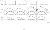
- FIG. 6 is a waveform timing diagram in which the slope of the ripple signal of the current power converter remains unchanged at light load or heavy load.
- the direct current (DC) voltage value of the output voltage VOUT will drop during the load consuming period (for example, from 1.8V to 1.79V).
- the reasons are as follows: when the current value of the sensing signal IL related to the output current IOUT increases (for example, from 0 A to 10 A), the on-time of the PWM signal PWM increases due to the fixed frequency control, resulting in the increasing of the peak voltage reached by the rising part IU of the ripple signal VNP, and consequently the peak voltage reached by the second feedback signal FBI obtained by adding the ripple signal VNP to the first feedback signal FB also increases.
- the slope of the falling part ID of the ripple signal VNP remains the same as that at light load; therefore, it is too late for the falling part ID of the ripple signal VNP to drop to the lowest voltage value at the time TA (that is, when the PWM signal PWM changes from low level to high level), and a ripple offset VD is generated.
- the PWM signal PWM will change from low level to high level. Therefore, it is necessary to satisfy the condition that the reference voltage VREF is equal to the ripple offset VD plus the first feedback signal FB. Since the ripple offset VD will increase with the increasing of load consuming, the first feedback signal FB will relatively decrease with the increase of load consuming, which causes the output of the power converter to become unstable.
- the load consuming behavior causes the end point of the ripple signal VNP (or the second feedback signal FBI) to rise, which is equivalent to the rise of the reference voltage VREF, thus causing the direct current (DC) voltage value of the output voltage VOUT of the power converter to fall.
- FIG. 7 is a waveform timing diagram of the control circuit of the power converter of the invention that adjusts the slope of the falling part of the ripple signal under heavy load.
- the on-time of the PWM signal PWM increases due to the fixed frequency control, resulting in the increasing of the peak voltage reached by the rising part IU of the ripple signal VNP, and the peak voltage of the second feedback signal FBI obtained by adding the ripple signal VNP to the first feedback signal FB, also increases.
- the difference between the invention and the prior art is that the slope of the falling part ID 1 of the ripple signal VNP of the invention under heavy load will not remain the same as the slope under light load, but increases with the increasing of the load (that is, the current value of the sensing signal IL increases), so that the adjusted falling part ID 1 can be reduced to the lowest voltage value at the time TB (that is, the PWM signal PWM changes from low level to high level). Therefore, no ripple offset VD will be generated, and the second feedback signal FBI will not decrease with the increase of the consuming, so as to achieve a stable output of the power converter.
- Another embodiment according to the invention is a control method of a power converter.
- the control method is used to control an output stage of the power converter to convert an input voltage into an output voltage and generate an output current.
- FIG. 8 is a flowchart of the control method of the power converter in this embodiment. As shown in FIG. 8 , the control method includes the following steps of:
- Step S 10 generating a ripple signal according to an input voltage, an output voltage and an output current of the power converter
- Step S 12 generating a second feedback signal according to the ripple signal and the first feedback signal, wherein the first feedback signal is related to the output voltage;
- Step S 14 generating an error signal according to the second feedback signal and the reference voltage
- Step S 16 generating a comparison signal according to the ramp signal and the error signal.
- Step S 18 generating a PWM signal according to the comparison signal to control the output stage, and the slope of the ripple signal changes with the output current.
- the ripple signal generated in the step S 10 includes a rising part and a falling part, and a slope of the falling part changes with the output current. For example, when the output current is larger, the slope of the falling part is larger, and vice versa.
- the step S 10 can generate the rising part according to the input voltage and the output voltage and generate the falling part according to the output voltage and the output current, but not limited to this.
- control method further selectively outputs the rising part and the falling part as the ripple signal according to the PWM signal.
- control method can also sense the output current from the output stage and provide a sensing signal, and generate a current signal according to the sensing signal to adjust the slope of the falling part.
- the adjusted falling part will be equal to the falling part before adjustment plus the current signal.
- the current signal is K times the sensing signal, and K is a magnification, but not limited to this.
- the above control method can also sense the output current from the output stage and provide a sensing signal, and generate a voltage signal according to the sensing signal and the output voltage to adjust the slope of the falling part.
- the voltage signal will be equal to the output voltage plus K times the sensing signal, and K is a magnification, but not limited to this.
- control circuit and the control method of the power converter of the invention have the following advantages/effects:
Landscapes
- Engineering & Computer Science (AREA)
- Power Engineering (AREA)
- Dc-Dc Converters (AREA)
Applications Claiming Priority (2)
| Application Number | Priority Date | Filing Date | Title |
|---|---|---|---|
| CN202010558675.3 | 2020-06-18 | ||
| CN202010558675.3A CN113824318A (zh) | 2020-06-18 | 2020-06-18 | 电源转换器的控制电路及其控制方法 |
Publications (2)
| Publication Number | Publication Date |
|---|---|
| US20210399635A1 US20210399635A1 (en) | 2021-12-23 |
| US11502601B2 true US11502601B2 (en) | 2022-11-15 |
Family
ID=78911665
Family Applications (1)
| Application Number | Title | Priority Date | Filing Date |
|---|---|---|---|
| US17/341,437 Active US11502601B2 (en) | 2020-06-18 | 2021-06-08 | Control circuit and control method of power converter |
Country Status (2)
| Country | Link |
|---|---|
| US (1) | US11502601B2 (zh) |
| CN (1) | CN113824318A (zh) |
Cited By (1)
| Publication number | Priority date | Publication date | Assignee | Title |
|---|---|---|---|---|
| US11909322B2 (en) * | 2020-12-11 | 2024-02-20 | Wuxi Si-Power Micro-Electronics Co., Ltd. | Isolation type power conversion method based on demagnetization iteration control and power conversion circuit |
Families Citing this family (1)
| Publication number | Priority date | Publication date | Assignee | Title |
|---|---|---|---|---|
| TW202326337A (zh) * | 2021-12-17 | 2023-07-01 | 力智電子股份有限公司 | 電源轉換器的智慧功率級電路及其電流監測電路 |
Citations (13)
| Publication number | Priority date | Publication date | Assignee | Title |
|---|---|---|---|---|
| US6791306B2 (en) * | 2002-01-29 | 2004-09-14 | Intersil Americas Inc. | Synthetic ripple regulator |
| US7482793B2 (en) | 2006-09-11 | 2009-01-27 | Micrel, Inc. | Ripple generation in buck regulator using fixed on-time control to enable the use of output capacitor having any ESR |
| US7482791B2 (en) | 2006-09-11 | 2009-01-27 | Micrel, Inc. | Constant on-time regulator with internal ripple generation and improved output voltage accuracy |
| US8446135B2 (en) * | 2011-02-24 | 2013-05-21 | Richtek Technology Corp. | Control circuit and method for a ripple regulator system |
| US8766615B2 (en) * | 2011-09-13 | 2014-07-01 | Ricoh Company, Ltd. | DC-DC converter control circuit and DC-DC converter including same |
| US9030177B2 (en) * | 2011-04-28 | 2015-05-12 | Mitsumi Electric Co., Ltd. | Switched-mode power supply having an adaptive on-time function and controlling output with a ripple control method |
| US9065337B2 (en) | 2013-02-25 | 2015-06-23 | Analog Devices Global | Inductor current emulation circuit for a switching converter |
| US9201438B2 (en) * | 2012-11-15 | 2015-12-01 | Micrel, Inc. | Buck DC-DC converter with accuracy enhancement |
| US9214866B2 (en) | 2013-06-21 | 2015-12-15 | Micrel, Inc. | Current sharing method for COT buck converter |
| US9306454B2 (en) | 2013-05-23 | 2016-04-05 | Micrel, Inc. | Optimal ripple injection for a boost regulator |
| US9588532B2 (en) | 2012-03-26 | 2017-03-07 | Infineon Technologies Americas Corp. | Voltage regulator having an emulated ripple generator |
| US9729058B2 (en) | 2015-09-22 | 2017-08-08 | Stmicroelectronics S.R.L. | Converter circuit with injection of ripple current for comparison |
| US10218274B1 (en) | 2017-12-22 | 2019-02-26 | Nxp B.V. | System and method for generating a ripple voltage for a ripple based constant-on-time DC-DC converter |
-
2020
- 2020-06-18 CN CN202010558675.3A patent/CN113824318A/zh active Pending
-
2021
- 2021-06-08 US US17/341,437 patent/US11502601B2/en active Active
Patent Citations (13)
| Publication number | Priority date | Publication date | Assignee | Title |
|---|---|---|---|---|
| US6791306B2 (en) * | 2002-01-29 | 2004-09-14 | Intersil Americas Inc. | Synthetic ripple regulator |
| US7482793B2 (en) | 2006-09-11 | 2009-01-27 | Micrel, Inc. | Ripple generation in buck regulator using fixed on-time control to enable the use of output capacitor having any ESR |
| US7482791B2 (en) | 2006-09-11 | 2009-01-27 | Micrel, Inc. | Constant on-time regulator with internal ripple generation and improved output voltage accuracy |
| US8446135B2 (en) * | 2011-02-24 | 2013-05-21 | Richtek Technology Corp. | Control circuit and method for a ripple regulator system |
| US9030177B2 (en) * | 2011-04-28 | 2015-05-12 | Mitsumi Electric Co., Ltd. | Switched-mode power supply having an adaptive on-time function and controlling output with a ripple control method |
| US8766615B2 (en) * | 2011-09-13 | 2014-07-01 | Ricoh Company, Ltd. | DC-DC converter control circuit and DC-DC converter including same |
| US9588532B2 (en) | 2012-03-26 | 2017-03-07 | Infineon Technologies Americas Corp. | Voltage regulator having an emulated ripple generator |
| US9201438B2 (en) * | 2012-11-15 | 2015-12-01 | Micrel, Inc. | Buck DC-DC converter with accuracy enhancement |
| US9065337B2 (en) | 2013-02-25 | 2015-06-23 | Analog Devices Global | Inductor current emulation circuit for a switching converter |
| US9306454B2 (en) | 2013-05-23 | 2016-04-05 | Micrel, Inc. | Optimal ripple injection for a boost regulator |
| US9214866B2 (en) | 2013-06-21 | 2015-12-15 | Micrel, Inc. | Current sharing method for COT buck converter |
| US9729058B2 (en) | 2015-09-22 | 2017-08-08 | Stmicroelectronics S.R.L. | Converter circuit with injection of ripple current for comparison |
| US10218274B1 (en) | 2017-12-22 | 2019-02-26 | Nxp B.V. | System and method for generating a ripple voltage for a ripple based constant-on-time DC-DC converter |
Cited By (1)
| Publication number | Priority date | Publication date | Assignee | Title |
|---|---|---|---|---|
| US11909322B2 (en) * | 2020-12-11 | 2024-02-20 | Wuxi Si-Power Micro-Electronics Co., Ltd. | Isolation type power conversion method based on demagnetization iteration control and power conversion circuit |
Also Published As
| Publication number | Publication date |
|---|---|
| US20210399635A1 (en) | 2021-12-23 |
| CN113824318A (zh) | 2021-12-21 |
Similar Documents
| Publication | Publication Date | Title |
|---|---|---|
| US8698476B2 (en) | Control circuit and method for a current mode controlled power converter | |
| US8253407B2 (en) | Voltage mode switching regulator and control circuit and method therefor | |
| CN100514813C (zh) | Dc-dc变换器及其控制单元和方法 | |
| US7723967B2 (en) | Step-up converter having an improved dynamic response | |
| US7193871B2 (en) | DC-DC converter circuit | |
| US10826380B2 (en) | Switching converter, circuit and method for controlling the same | |
| US11502601B2 (en) | Control circuit and control method of power converter | |
| CN114825926A (zh) | 用于混合转换器的脉宽调变控制器 | |
| TWI634728B (zh) | 運作於脈衝省略模式的控制電路及具有其之電壓轉換器 | |
| KR20130036065A (ko) | 벅 스위치 모드 파워 컨버터 큰 신호 천이 응답 최적화기 | |
| TWI513152B (zh) | 時間信號產生器及時間信號產生方法 | |
| US9966849B1 (en) | Current mode voltage converter having fast transient response | |
| US10128757B2 (en) | Buck-boost converter with small disturbance at mode transitions | |
| US10594209B2 (en) | Switching power converter circuit and control circuit thereof | |
| US9467044B2 (en) | Timing generator and timing signal generation method for power converter | |
| US10193443B2 (en) | Systems and methods for enhancing dynamic response of power conversion systems | |
| US20230327552A1 (en) | Switching power supply, and control circuit and control method thereof | |
| CN114389452A (zh) | 开关变换器及其控制电路和控制方法 | |
| CN115378246B (zh) | 具有过冲保护的开关电源 | |
| US20240235366A1 (en) | Switching converter and control circuit thereof | |
| US11616431B2 (en) | Control circuit of power converter | |
| CN112448578B (zh) | 开关电源电路 | |
| US20200266710A1 (en) | Control circuit of buck-boost converting apparatus and mode switching method of the same | |
| US11621637B2 (en) | Control circuit of power converter | |
| KR102502763B1 (ko) | 커패시터 공유 방식의 소프트 스타트업 회로 및 이를 포함하는 스위치 제어 회로 및 dc-dc 컨버터 |
Legal Events
| Date | Code | Title | Description |
|---|---|---|---|
| AS | Assignment |
Owner name: UPI SEMICONDUCTOR CORP., TAIWAN Free format text: ASSIGNMENT OF ASSIGNORS INTEREST;ASSIGNORS:CHANG, CHIH-LIEN;WANG, CHUN-CHIEH;REEL/FRAME:056463/0039 Effective date: 20210602 |
|
| FEPP | Fee payment procedure |
Free format text: ENTITY STATUS SET TO UNDISCOUNTED (ORIGINAL EVENT CODE: BIG.); ENTITY STATUS OF PATENT OWNER: LARGE ENTITY |
|
| STPP | Information on status: patent application and granting procedure in general |
Free format text: DOCKETED NEW CASE - READY FOR EXAMINATION |
|
| STPP | Information on status: patent application and granting procedure in general |
Free format text: NON FINAL ACTION MAILED |
|
| STPP | Information on status: patent application and granting procedure in general |
Free format text: RESPONSE TO NON-FINAL OFFICE ACTION ENTERED AND FORWARDED TO EXAMINER |
|
| STPP | Information on status: patent application and granting procedure in general |
Free format text: NOTICE OF ALLOWANCE MAILED -- APPLICATION RECEIVED IN OFFICE OF PUBLICATIONS |
|
| STPP | Information on status: patent application and granting procedure in general |
Free format text: PUBLICATIONS -- ISSUE FEE PAYMENT RECEIVED |
|
| STCF | Information on status: patent grant |
Free format text: PATENTED CASE |