US11492344B2 - Organic molecules for use in organic optoelectronic devices - Google Patents
Organic molecules for use in organic optoelectronic devices Download PDFInfo
- Publication number
- US11492344B2 US11492344B2 US16/329,052 US201716329052A US11492344B2 US 11492344 B2 US11492344 B2 US 11492344B2 US 201716329052 A US201716329052 A US 201716329052A US 11492344 B2 US11492344 B2 US 11492344B2
- Authority
- US
- United States
- Prior art keywords
- group
- atoms
- radicals
- substituted
- replaced
- Prior art date
- Legal status (The legal status is an assumption and is not a legal conclusion. Google has not performed a legal analysis and makes no representation as to the accuracy of the status listed.)
- Active, expires
Links
- 230000005693 optoelectronics Effects 0.000 title claims description 37
- 239000000126 substance Substances 0.000 claims abstract description 53
- 125000003118 aryl group Chemical group 0.000 claims description 50
- 229910052799 carbon Inorganic materials 0.000 claims description 46
- 239000000463 material Substances 0.000 claims description 43
- 229910052760 oxygen Inorganic materials 0.000 claims description 31
- 229910052717 sulfur Inorganic materials 0.000 claims description 31
- 125000004432 carbon atom Chemical group C* 0.000 claims description 30
- YZCKVEUIGOORGS-OUBTZVSYSA-N Deuterium Chemical compound [2H] YZCKVEUIGOORGS-OUBTZVSYSA-N 0.000 claims description 26
- 229910052805 deuterium Inorganic materials 0.000 claims description 26
- 125000003342 alkenyl group Chemical group 0.000 claims description 21
- 125000006193 alkinyl group Chemical group 0.000 claims description 21
- 125000004435 hydrogen atom Chemical group [H]* 0.000 claims description 21
- 125000003545 alkoxy group Chemical group 0.000 claims description 20
- 125000005309 thioalkoxy group Chemical group 0.000 claims description 19
- 239000000758 substrate Substances 0.000 claims description 17
- 229910052710 silicon Inorganic materials 0.000 claims description 16
- 239000000203 mixture Substances 0.000 claims description 13
- 125000000217 alkyl group Chemical group 0.000 claims description 11
- 125000006165 cyclic alkyl group Chemical group 0.000 claims description 11
- 238000000034 method Methods 0.000 claims description 10
- 125000004104 aryloxy group Chemical group 0.000 claims description 9
- 125000004986 diarylamino group Chemical group 0.000 claims description 9
- 125000005240 diheteroarylamino group Chemical group 0.000 claims description 9
- 229910052731 fluorine Inorganic materials 0.000 claims description 9
- 125000005553 heteroaryloxy group Chemical group 0.000 claims description 9
- 229910052739 hydrogen Inorganic materials 0.000 claims description 8
- 239000002904 solvent Substances 0.000 claims description 8
- XSXHWVKGUXMUQE-UHFFFAOYSA-N osmium dioxide Inorganic materials O=[Os]=O XSXHWVKGUXMUQE-UHFFFAOYSA-N 0.000 claims description 7
- 125000001997 phenyl group Chemical group [H]C1=C([H])C([H])=C(*)C([H])=C1[H] 0.000 claims description 5
- 125000000609 carbazolyl group Chemical group C1(=CC=CC=2C3=CC=CC=C3NC12)* 0.000 claims description 4
- 238000006243 chemical reaction Methods 0.000 claims description 4
- 125000002496 methyl group Chemical group [H]C([H])([H])* 0.000 claims description 4
- 230000005669 field effect Effects 0.000 claims description 3
- 125000002950 monocyclic group Chemical group 0.000 claims description 3
- 125000003367 polycyclic group Chemical group 0.000 claims description 3
- 125000004076 pyridyl group Chemical group 0.000 claims description 3
- 125000000714 pyrimidinyl group Chemical group 0.000 claims description 3
- 125000004306 triazinyl group Chemical group 0.000 claims description 3
- 125000001931 aliphatic group Chemical group 0.000 claims description 2
- 125000004122 cyclic group Chemical group 0.000 claims description 2
- 239000000975 dye Substances 0.000 claims description 2
- 238000012545 processing Methods 0.000 claims description 2
- 229910052721 tungsten Inorganic materials 0.000 claims description 2
- 229910052720 vanadium Inorganic materials 0.000 claims description 2
- 230000008020 evaporation Effects 0.000 claims 1
- 238000001704 evaporation Methods 0.000 claims 1
- 239000010410 layer Substances 0.000 description 91
- 0 [1*]c1nc([1*])nc(-c2c([3H])c([V])c([W])c(C)c2[Y])n1 Chemical compound [1*]c1nc([1*])nc(-c2c([3H])c([V])c([W])c(C)c2[Y])n1 0.000 description 55
- -1 metal complex compounds Chemical class 0.000 description 55
- 150000003254 radicals Chemical group 0.000 description 32
- 125000002023 trifluoromethyl group Chemical group FC(F)(F)* 0.000 description 31
- 125000001449 isopropyl group Chemical group [H]C([H])([H])C([H])(*)C([H])([H])[H] 0.000 description 18
- 125000000999 tert-butyl group Chemical group [H]C([H])([H])C(*)(C([H])([H])[H])C([H])([H])[H] 0.000 description 18
- UHOVQNZJYSORNB-UHFFFAOYSA-N Benzene Chemical compound C1=CC=CC=C1 UHOVQNZJYSORNB-UHFFFAOYSA-N 0.000 description 15
- 238000000295 emission spectrum Methods 0.000 description 15
- 229920003229 poly(methyl methacrylate) Polymers 0.000 description 14
- 239000004926 polymethyl methacrylate Substances 0.000 description 14
- 230000015572 biosynthetic process Effects 0.000 description 13
- 238000006862 quantum yield reaction Methods 0.000 description 13
- 238000003786 synthesis reaction Methods 0.000 description 12
- 238000005424 photoluminescence Methods 0.000 description 10
- 241001655883 Adeno-associated virus - 1 Species 0.000 description 9
- 239000000243 solution Substances 0.000 description 9
- DDGPPAMADXTGTN-UHFFFAOYSA-N 2-chloro-4,6-diphenyl-1,3,5-triazine Chemical compound N=1C(Cl)=NC(C=2C=CC=CC=2)=NC=1C1=CC=CC=C1 DDGPPAMADXTGTN-UHFFFAOYSA-N 0.000 description 8
- UJOBWOGCFQCDNV-UHFFFAOYSA-N 9H-carbazole Chemical compound C1=CC=C2C3=CC=CC=C3NC2=C1 UJOBWOGCFQCDNV-UHFFFAOYSA-N 0.000 description 8
- 241001164823 Adeno-associated virus - 7 Species 0.000 description 8
- 230000000903 blocking effect Effects 0.000 description 7
- 238000004519 manufacturing process Methods 0.000 description 7
- IJGRMHOSHXDMSA-UHFFFAOYSA-N nitrogen Substances N#N IJGRMHOSHXDMSA-UHFFFAOYSA-N 0.000 description 7
- YMWUJEATGCHHMB-UHFFFAOYSA-N Dichloromethane Chemical compound ClCCl YMWUJEATGCHHMB-UHFFFAOYSA-N 0.000 description 6
- IAZDPXIOMUYVGZ-UHFFFAOYSA-N Dimethylsulphoxide Chemical compound CS(C)=O IAZDPXIOMUYVGZ-UHFFFAOYSA-N 0.000 description 6
- YXFVVABEGXRONW-UHFFFAOYSA-N Toluene Chemical compound CC1=CC=CC=C1 YXFVVABEGXRONW-UHFFFAOYSA-N 0.000 description 6
- 125000001072 heteroaryl group Chemical group 0.000 description 6
- 238000002347 injection Methods 0.000 description 6
- 239000007924 injection Substances 0.000 description 6
- WEVYAHXRMPXWCK-UHFFFAOYSA-N Acetonitrile Chemical compound CC#N WEVYAHXRMPXWCK-UHFFFAOYSA-N 0.000 description 5
- ZMXDDKWLCZADIW-UHFFFAOYSA-N N,N-Dimethylformamide Chemical compound CN(C)C=O ZMXDDKWLCZADIW-UHFFFAOYSA-N 0.000 description 5
- 238000000589 high-performance liquid chromatography-mass spectrometry Methods 0.000 description 5
- 238000004770 highest occupied molecular orbital Methods 0.000 description 5
- 238000004768 lowest unoccupied molecular orbital Methods 0.000 description 5
- 229910052757 nitrogen Inorganic materials 0.000 description 5
- 238000001161 time-correlated single photon counting Methods 0.000 description 5
- LWIHDJKSTIGBAC-UHFFFAOYSA-K tripotassium phosphate Chemical compound [K+].[K+].[K+].[O-]P([O-])([O-])=O LWIHDJKSTIGBAC-UHFFFAOYSA-K 0.000 description 5
- YKYMGFVDWOIHJH-UHFFFAOYSA-N (4-cyano-3,5-difluorophenyl)boronic acid Chemical compound OB(O)C1=CC(F)=C(C#N)C(F)=C1 YKYMGFVDWOIHJH-UHFFFAOYSA-N 0.000 description 4
- MMNNWKCYXNXWBG-UHFFFAOYSA-N 2,4,6-tris(3-phenylphenyl)-1,3,5-triazine Chemical compound C1=CC=CC=C1C1=CC=CC(C=2N=C(N=C(N=2)C=2C=C(C=CC=2)C=2C=CC=CC=2)C=2C=C(C=CC=2)C=2C=CC=CC=2)=C1 MMNNWKCYXNXWBG-UHFFFAOYSA-N 0.000 description 4
- AWXGSYPUMWKTBR-UHFFFAOYSA-N 4-carbazol-9-yl-n,n-bis(4-carbazol-9-ylphenyl)aniline Chemical compound C12=CC=CC=C2C2=CC=CC=C2N1C1=CC=C(N(C=2C=CC(=CC=2)N2C3=CC=CC=C3C3=CC=CC=C32)C=2C=CC(=CC=2)N2C3=CC=CC=C3C3=CC=CC=C32)C=C1 AWXGSYPUMWKTBR-UHFFFAOYSA-N 0.000 description 4
- YEWVLWWLYHXZLZ-UHFFFAOYSA-N 9-(3-dibenzofuran-2-ylphenyl)carbazole Chemical compound C1=CC=C2C3=CC(C=4C=CC=C(C=4)N4C5=CC=CC=C5C5=CC=CC=C54)=CC=C3OC2=C1 YEWVLWWLYHXZLZ-UHFFFAOYSA-N 0.000 description 4
- VFUDMQLBKNMONU-UHFFFAOYSA-N 9-[4-(4-carbazol-9-ylphenyl)phenyl]carbazole Chemical compound C12=CC=CC=C2C2=CC=CC=C2N1C1=CC=C(C=2C=CC(=CC=2)N2C3=CC=CC=C3C3=CC=CC=C32)C=C1 VFUDMQLBKNMONU-UHFFFAOYSA-N 0.000 description 4
- 241000702423 Adeno-associated virus - 2 Species 0.000 description 4
- LFQSCWFLJHTTHZ-UHFFFAOYSA-N Ethanol Chemical compound CCO LFQSCWFLJHTTHZ-UHFFFAOYSA-N 0.000 description 4
- CSNNHWWHGAXBCP-UHFFFAOYSA-L Magnesium sulfate Chemical compound [Mg+2].[O-][S+2]([O-])([O-])[O-] CSNNHWWHGAXBCP-UHFFFAOYSA-L 0.000 description 4
- JUJWROOIHBZHMG-UHFFFAOYSA-N Pyridine Chemical compound C1=CC=NC=C1 JUJWROOIHBZHMG-UHFFFAOYSA-N 0.000 description 4
- SMWDFEZZVXVKRB-UHFFFAOYSA-N Quinoline Chemical compound N1=CC=CC2=CC=CC=C21 SMWDFEZZVXVKRB-UHFFFAOYSA-N 0.000 description 4
- FAPWRFPIFSIZLT-UHFFFAOYSA-M Sodium chloride Chemical class [Na+].[Cl-] FAPWRFPIFSIZLT-UHFFFAOYSA-M 0.000 description 4
- WYURNTSHIVDZCO-UHFFFAOYSA-N Tetrahydrofuran Chemical compound C1CCOC1 WYURNTSHIVDZCO-UHFFFAOYSA-N 0.000 description 4
- YTPLMLYBLZKORZ-UHFFFAOYSA-N Thiophene Chemical compound C=1C=CSC=1 YTPLMLYBLZKORZ-UHFFFAOYSA-N 0.000 description 4
- XLOMVQKBTHCTTD-UHFFFAOYSA-N Zinc monoxide Chemical compound [Zn]=O XLOMVQKBTHCTTD-UHFFFAOYSA-N 0.000 description 4
- MWPLVEDNUUSJAV-UHFFFAOYSA-N anthracene Chemical compound C1=CC=CC2=CC3=CC=CC=C3C=C21 MWPLVEDNUUSJAV-UHFFFAOYSA-N 0.000 description 4
- 150000001716 carbazoles Chemical class 0.000 description 4
- 238000000576 coating method Methods 0.000 description 4
- 238000005538 encapsulation Methods 0.000 description 4
- 239000010408 film Substances 0.000 description 4
- 239000007789 gas Substances 0.000 description 4
- AWJUIBRHMBBTKR-UHFFFAOYSA-N isoquinoline Chemical compound C1=NC=CC2=CC=CC=C21 AWJUIBRHMBBTKR-UHFFFAOYSA-N 0.000 description 4
- 239000011159 matrix material Substances 0.000 description 4
- 238000005259 measurement Methods 0.000 description 4
- YNPNZTXNASCQKK-UHFFFAOYSA-N phenanthrene Chemical compound C1=CC=C2C3=CC=CC=C3C=CC2=C1 YNPNZTXNASCQKK-UHFFFAOYSA-N 0.000 description 4
- 230000003595 spectral effect Effects 0.000 description 4
- XLYOFNOQVPJJNP-UHFFFAOYSA-N water Substances O XLYOFNOQVPJJNP-UHFFFAOYSA-N 0.000 description 4
- TXBFHHYSJNVGBX-UHFFFAOYSA-N (4-diphenylphosphorylphenyl)-triphenylsilane Chemical compound C=1C=CC=CC=1P(C=1C=CC(=CC=1)[Si](C=1C=CC=CC=1)(C=1C=CC=CC=1)C=1C=CC=CC=1)(=O)C1=CC=CC=C1 TXBFHHYSJNVGBX-UHFFFAOYSA-N 0.000 description 3
- XOYZGLGJSAZOAG-UHFFFAOYSA-N 1-n,1-n,4-n-triphenyl-4-n-[4-[4-(n-[4-(n-phenylanilino)phenyl]anilino)phenyl]phenyl]benzene-1,4-diamine Chemical compound C1=CC=CC=C1N(C=1C=CC(=CC=1)N(C=1C=CC=CC=1)C=1C=CC(=CC=1)C=1C=CC(=CC=1)N(C=1C=CC=CC=1)C=1C=CC(=CC=1)N(C=1C=CC=CC=1)C=1C=CC=CC=1)C1=CC=CC=C1 XOYZGLGJSAZOAG-UHFFFAOYSA-N 0.000 description 3
- MQRCTQVBZYBPQE-UHFFFAOYSA-N 189363-47-1 Chemical compound C1=CC=CC=C1N(C=1C=C2C3(C4=CC(=CC=C4C2=CC=1)N(C=1C=CC=CC=1)C=1C=CC=CC=1)C1=CC(=CC=C1C1=CC=C(C=C13)N(C=1C=CC=CC=1)C=1C=CC=CC=1)N(C=1C=CC=CC=1)C=1C=CC=CC=1)C1=CC=CC=C1 MQRCTQVBZYBPQE-UHFFFAOYSA-N 0.000 description 3
- XESMNQMWRSEIET-UHFFFAOYSA-N 2,9-dinaphthalen-2-yl-4,7-diphenyl-1,10-phenanthroline Chemical compound C1=CC=CC=C1C1=CC(C=2C=C3C=CC=CC3=CC=2)=NC2=C1C=CC1=C(C=3C=CC=CC=3)C=C(C=3C=C4C=CC=CC4=CC=3)N=C21 XESMNQMWRSEIET-UHFFFAOYSA-N 0.000 description 3
- PWJYOTPKLOICJK-UHFFFAOYSA-N 2-methyl-9h-carbazole Chemical compound C1=CC=C2C3=CC=C(C)C=C3NC2=C1 PWJYOTPKLOICJK-UHFFFAOYSA-N 0.000 description 3
- 229920001621 AMOLED Polymers 0.000 description 3
- XEKOWRVHYACXOJ-UHFFFAOYSA-N Ethyl acetate Chemical compound CCOC(C)=O XEKOWRVHYACXOJ-UHFFFAOYSA-N 0.000 description 3
- YLQBMQCUIZJEEH-UHFFFAOYSA-N Furan Chemical compound C=1C=COC=1 YLQBMQCUIZJEEH-UHFFFAOYSA-N 0.000 description 3
- 101000837344 Homo sapiens T-cell leukemia translocation-altered gene protein Proteins 0.000 description 3
- 102100028692 T-cell leukemia translocation-altered gene protein Human genes 0.000 description 3
- 125000003636 chemical group Chemical group 0.000 description 3
- 150000001875 compounds Chemical class 0.000 description 3
- 239000002019 doping agent Substances 0.000 description 3
- 230000005284 excitation Effects 0.000 description 3
- GVEPBJHOBDJJJI-UHFFFAOYSA-N fluoranthrene Natural products C1=CC(C2=CC=CC=C22)=C3C2=CC=CC3=C1 GVEPBJHOBDJJJI-UHFFFAOYSA-N 0.000 description 3
- 239000011521 glass Substances 0.000 description 3
- 125000005842 heteroatom Chemical group 0.000 description 3
- RAXXELZNTBOGNW-UHFFFAOYSA-N imidazole Natural products C1=CNC=N1 RAXXELZNTBOGNW-UHFFFAOYSA-N 0.000 description 3
- 229910052751 metal Inorganic materials 0.000 description 3
- 239000002184 metal Substances 0.000 description 3
- 239000007787 solid Substances 0.000 description 3
- MQZKXUUUSIAJDE-UHFFFAOYSA-N (2-cyano-4,5-difluorophenyl)boronic acid Chemical compound OB(O)C1=CC(F)=C(F)C=C1C#N MQZKXUUUSIAJDE-UHFFFAOYSA-N 0.000 description 2
- UQMRRVKHBGKIAF-UHFFFAOYSA-N (4-cyano-2,5-difluorophenyl)boronic acid Chemical compound OB(O)C1=CC(F)=C(C#N)C=C1F UQMRRVKHBGKIAF-UHFFFAOYSA-N 0.000 description 2
- WABHFLPVEUGDMT-UHFFFAOYSA-N (4-cyano-2,6-difluorophenyl)boronic acid Chemical compound OB(O)C1=C(F)C=C(C#N)C=C1F WABHFLPVEUGDMT-UHFFFAOYSA-N 0.000 description 2
- FCEHBMOGCRZNNI-UHFFFAOYSA-N 1-benzothiophene Chemical compound C1=CC=C2SC=CC2=C1 FCEHBMOGCRZNNI-UHFFFAOYSA-N 0.000 description 2
- ATTVYRDSOVWELU-UHFFFAOYSA-N 1-diphenylphosphoryl-2-(2-diphenylphosphorylphenoxy)benzene Chemical compound C=1C=CC=CC=1P(C=1C(=CC=CC=1)OC=1C(=CC=CC=1)P(=O)(C=1C=CC=CC=1)C=1C=CC=CC=1)(=O)C1=CC=CC=C1 ATTVYRDSOVWELU-UHFFFAOYSA-N 0.000 description 2
- SPDPTFAJSFKAMT-UHFFFAOYSA-N 1-n-[4-[4-(n-[4-(3-methyl-n-(3-methylphenyl)anilino)phenyl]anilino)phenyl]phenyl]-4-n,4-n-bis(3-methylphenyl)-1-n-phenylbenzene-1,4-diamine Chemical compound CC1=CC=CC(N(C=2C=CC(=CC=2)N(C=2C=CC=CC=2)C=2C=CC(=CC=2)C=2C=CC(=CC=2)N(C=2C=CC=CC=2)C=2C=CC(=CC=2)N(C=2C=C(C)C=CC=2)C=2C=C(C)C=CC=2)C=2C=C(C)C=CC=2)=C1 SPDPTFAJSFKAMT-UHFFFAOYSA-N 0.000 description 2
- GKWLILHTTGWKLQ-UHFFFAOYSA-N 2,3-dihydrothieno[3,4-b][1,4]dioxine Chemical compound O1CCOC2=CSC=C21 GKWLILHTTGWKLQ-UHFFFAOYSA-N 0.000 description 2
- STTGYIUESPWXOW-UHFFFAOYSA-N 2,9-dimethyl-4,7-diphenyl-1,10-phenanthroline Chemical compound C=12C=CC3=C(C=4C=CC=CC=4)C=C(C)N=C3C2=NC(C)=CC=1C1=CC=CC=C1 STTGYIUESPWXOW-UHFFFAOYSA-N 0.000 description 2
- HJRPDUSMHNOSPO-UHFFFAOYSA-N 2-[3,5-difluoro-4-(trifluoromethyl)phenyl]-4,4,5,5-tetramethyl-1,3,2-dioxaborolane Chemical compound O1C(C)(C)C(C)(C)OB1C1=CC(F)=C(C(F)(F)F)C(F)=C1 HJRPDUSMHNOSPO-UHFFFAOYSA-N 0.000 description 2
- IXHWGNYCZPISET-UHFFFAOYSA-N 2-[4-(dicyanomethylidene)-2,3,5,6-tetrafluorocyclohexa-2,5-dien-1-ylidene]propanedinitrile Chemical compound FC1=C(F)C(=C(C#N)C#N)C(F)=C(F)C1=C(C#N)C#N IXHWGNYCZPISET-UHFFFAOYSA-N 0.000 description 2
- IIKVAWLYHHZRGV-UHFFFAOYSA-N 2-carbazol-9-ylethanol Chemical compound C1=CC=C2N(CCO)C3=CC=CC=C3C2=C1 IIKVAWLYHHZRGV-UHFFFAOYSA-N 0.000 description 2
- HTSVYUUXJSMGQC-UHFFFAOYSA-N 2-chloro-1,3,5-triazine Chemical compound ClC1=NC=NC=N1 HTSVYUUXJSMGQC-UHFFFAOYSA-N 0.000 description 2
- PHKYYUQQYARDIU-UHFFFAOYSA-N 3-methyl-9h-carbazole Chemical compound C1=CC=C2C3=CC(C)=CC=C3NC2=C1 PHKYYUQQYARDIU-UHFFFAOYSA-N 0.000 description 2
- ZOKIJILZFXPFTO-UHFFFAOYSA-N 4-methyl-n-[4-[1-[4-(4-methyl-n-(4-methylphenyl)anilino)phenyl]cyclohexyl]phenyl]-n-(4-methylphenyl)aniline Chemical compound C1=CC(C)=CC=C1N(C=1C=CC(=CC=1)C1(CCCCC1)C=1C=CC(=CC=1)N(C=1C=CC(C)=CC=1)C=1C=CC(C)=CC=1)C1=CC=C(C)C=C1 ZOKIJILZFXPFTO-UHFFFAOYSA-N 0.000 description 2
- DIVZFUBWFAOMCW-UHFFFAOYSA-N 4-n-(3-methylphenyl)-1-n,1-n-bis[4-(n-(3-methylphenyl)anilino)phenyl]-4-n-phenylbenzene-1,4-diamine Chemical compound CC1=CC=CC(N(C=2C=CC=CC=2)C=2C=CC(=CC=2)N(C=2C=CC(=CC=2)N(C=2C=CC=CC=2)C=2C=C(C)C=CC=2)C=2C=CC(=CC=2)N(C=2C=CC=CC=2)C=2C=C(C)C=CC=2)=C1 DIVZFUBWFAOMCW-UHFFFAOYSA-N 0.000 description 2
- KDCGOANMDULRCW-UHFFFAOYSA-N 7H-purine Chemical compound N1=CNC2=NC=NC2=C1 KDCGOANMDULRCW-UHFFFAOYSA-N 0.000 description 2
- ZLHINBZEEMIWIR-UHFFFAOYSA-N 9-(3-dibenzothiophen-2-ylphenyl)carbazole Chemical compound C1=CC=C2C3=CC(C=4C=CC=C(C=4)N4C5=CC=CC=C5C5=CC=CC=C54)=CC=C3SC2=C1 ZLHINBZEEMIWIR-UHFFFAOYSA-N 0.000 description 2
- WHMHUGLMCAFKFE-UHFFFAOYSA-N 9-[3,5-di(dibenzofuran-2-yl)phenyl]carbazole Chemical compound C1=CC=C2C3=CC(C=4C=C(C=C(C=4)N4C5=CC=CC=C5C5=CC=CC=C54)C4=CC=C5OC=6C(C5=C4)=CC=CC=6)=CC=C3OC2=C1 WHMHUGLMCAFKFE-UHFFFAOYSA-N 0.000 description 2
- FXKMXDQBHDTQII-UHFFFAOYSA-N 9-phenyl-3,6-bis(9-phenylcarbazol-3-yl)carbazole Chemical compound C1=CC=CC=C1N1C2=CC=C(C=3C=C4C5=CC(=CC=C5N(C=5C=CC=CC=5)C4=CC=3)C=3C=C4C5=CC=CC=C5N(C=5C=CC=CC=5)C4=CC=3)C=C2C2=CC=CC=C21 FXKMXDQBHDTQII-UHFFFAOYSA-N 0.000 description 2
- CSCPPACGZOOCGX-UHFFFAOYSA-N Acetone Chemical compound CC(C)=O CSCPPACGZOOCGX-UHFFFAOYSA-N 0.000 description 2
- 241001634120 Adeno-associated virus - 5 Species 0.000 description 2
- NVEAVAGNVGVABL-UHFFFAOYSA-N Cc1c(C)c(C)c2c(c1C)Cc1c(C)c(C)c(C)c(C)c1N2C Chemical compound Cc1c(C)c(C)c2c(c1C)Cc1c(C)c(C)c(C)c(C)c1N2C NVEAVAGNVGVABL-UHFFFAOYSA-N 0.000 description 2
- MTTYEQXMRZYHGK-UHFFFAOYSA-N Cc1c(C)c(C)c2c(c1C)c1c(C)c(C)c(C)c(C)c1n2C Chemical compound Cc1c(C)c(C)c2c(c1C)c1c(C)c(C)c(C)c(C)c1n2C MTTYEQXMRZYHGK-UHFFFAOYSA-N 0.000 description 2
- SIKJAQJRHWYJAI-UHFFFAOYSA-N Indole Chemical compound C1=CC=C2NC=CC2=C1 SIKJAQJRHWYJAI-UHFFFAOYSA-N 0.000 description 2
- CPLXHLVBOLITMK-UHFFFAOYSA-N Magnesium oxide Chemical compound [Mg]=O CPLXHLVBOLITMK-UHFFFAOYSA-N 0.000 description 2
- UFWIBTONFRDIAS-UHFFFAOYSA-N Naphthalene Chemical compound C1=CC=CC2=CC=CC=C21 UFWIBTONFRDIAS-UHFFFAOYSA-N 0.000 description 2
- PCNDJXKNXGMECE-UHFFFAOYSA-N Phenazine Natural products C1=CC=CC2=NC3=CC=CC=C3N=C21 PCNDJXKNXGMECE-UHFFFAOYSA-N 0.000 description 2
- 229920001609 Poly(3,4-ethylenedioxythiophene) Polymers 0.000 description 2
- KYQCOXFCLRTKLS-UHFFFAOYSA-N Pyrazine Chemical compound C1=CN=CC=N1 KYQCOXFCLRTKLS-UHFFFAOYSA-N 0.000 description 2
- CZPWVGJYEJSRLH-UHFFFAOYSA-N Pyrimidine Chemical compound C1=CN=CN=C1 CZPWVGJYEJSRLH-UHFFFAOYSA-N 0.000 description 2
- KAESVJOAVNADME-UHFFFAOYSA-N Pyrrole Chemical compound C=1C=CNC=1 KAESVJOAVNADME-UHFFFAOYSA-N 0.000 description 2
- GWEVSGVZZGPLCZ-UHFFFAOYSA-N Titan oxide Chemical compound O=[Ti]=O GWEVSGVZZGPLCZ-UHFFFAOYSA-N 0.000 description 2
- 239000007983 Tris buffer Substances 0.000 description 2
- WIHKEPSYODOQJR-UHFFFAOYSA-N [9-(4-tert-butylphenyl)-6-triphenylsilylcarbazol-3-yl]-triphenylsilane Chemical compound C1=CC(C(C)(C)C)=CC=C1N1C2=CC=C([Si](C=3C=CC=CC=3)(C=3C=CC=CC=3)C=3C=CC=CC=3)C=C2C2=CC([Si](C=3C=CC=CC=3)(C=3C=CC=CC=3)C=3C=CC=CC=3)=CC=C21 WIHKEPSYODOQJR-UHFFFAOYSA-N 0.000 description 2
- VIULCPVFRCFTJL-UHFFFAOYSA-N [C-]#[N+]c1cc(-n2c3ccccc3c3cc(-c4ccc(C#N)cc4C#N)ccc32)c(-n2c3ccccc3c3cc(-c4ccc(C#N)cc4C#N)ccc32)cc1-c1nc(-c2ccccc2)nc(-c2ccccc2)n1.[C-]#[N+]c1ccc(-c2ccc3c(c2)c2cc(-c4ccc(C#N)cc4[N+]#[C-])ccc2n3-c2cc([N+]#[C-])c(-c3nc(-c4ccccc4)nc(-c4ccccc4)n3)cc2-n2c3ccc(-c4ccc(C#N)cc4C#N)cc3c3cc(-c4ccc(C#N)cc4C#N)ccc32)c(C#N)c1.[C-]#[N+]c1ccc(-c2ccc3c4ccc(-c5ccc([N+]#[C-])cc5[N+]#[C-])cc4n(-c4cc(-c5nc(C)nc(C)n5)c(C#N)cc4-n4c5cc(-c6ccc(C#N)cc6C#N)ccc5c5ccc(-c6ccc(C#N)cc6[N+]#[C-])cc54)c3c2)c([N+]#[C-])c1.[C-]#[N+]c1ccc(-c2ccc3c4ccccc4n(-c4cc([N+]#[C-])c(-c5nc(C)nc(C)n5)cc4-n4c5ccccc5c5ccc(-c6ccc(C#N)cc6[N+]#[C-])cc54)c3c2)c(C#N)c1 Chemical compound [C-]#[N+]c1cc(-n2c3ccccc3c3cc(-c4ccc(C#N)cc4C#N)ccc32)c(-n2c3ccccc3c3cc(-c4ccc(C#N)cc4C#N)ccc32)cc1-c1nc(-c2ccccc2)nc(-c2ccccc2)n1.[C-]#[N+]c1ccc(-c2ccc3c(c2)c2cc(-c4ccc(C#N)cc4[N+]#[C-])ccc2n3-c2cc([N+]#[C-])c(-c3nc(-c4ccccc4)nc(-c4ccccc4)n3)cc2-n2c3ccc(-c4ccc(C#N)cc4C#N)cc3c3cc(-c4ccc(C#N)cc4C#N)ccc32)c(C#N)c1.[C-]#[N+]c1ccc(-c2ccc3c4ccc(-c5ccc([N+]#[C-])cc5[N+]#[C-])cc4n(-c4cc(-c5nc(C)nc(C)n5)c(C#N)cc4-n4c5cc(-c6ccc(C#N)cc6C#N)ccc5c5ccc(-c6ccc(C#N)cc6[N+]#[C-])cc54)c3c2)c([N+]#[C-])c1.[C-]#[N+]c1ccc(-c2ccc3c4ccccc4n(-c4cc([N+]#[C-])c(-c5nc(C)nc(C)n5)cc4-n4c5ccccc5c5ccc(-c6ccc(C#N)cc6[N+]#[C-])cc54)c3c2)c(C#N)c1 VIULCPVFRCFTJL-UHFFFAOYSA-N 0.000 description 2
- XHCLAFWTIXFWPH-UHFFFAOYSA-N [O-2].[O-2].[O-2].[O-2].[O-2].[V+5].[V+5] Chemical compound [O-2].[O-2].[O-2].[O-2].[O-2].[V+5].[V+5] XHCLAFWTIXFWPH-UHFFFAOYSA-N 0.000 description 2
- DZBUGLKDJFMEHC-UHFFFAOYSA-N acridine Chemical compound C1=CC=CC2=CC3=CC=CC=C3N=C21 DZBUGLKDJFMEHC-UHFFFAOYSA-N 0.000 description 2
- 229910052782 aluminium Inorganic materials 0.000 description 2
- 238000004458 analytical method Methods 0.000 description 2
- 238000000065 atmospheric pressure chemical ionisation Methods 0.000 description 2
- IOJUPLGTWVMSFF-UHFFFAOYSA-N benzothiazole Chemical compound C1=CC=C2SC=NC2=C1 IOJUPLGTWVMSFF-UHFFFAOYSA-N 0.000 description 2
- 238000005229 chemical vapour deposition Methods 0.000 description 2
- MVPPADPHJFYWMZ-UHFFFAOYSA-N chlorobenzene Chemical compound ClC1=CC=CC=C1 MVPPADPHJFYWMZ-UHFFFAOYSA-N 0.000 description 2
- WDECIBYCCFPHNR-UHFFFAOYSA-N chrysene Chemical compound C1=CC=CC2=CC=C3C4=CC=CC=C4C=CC3=C21 WDECIBYCCFPHNR-UHFFFAOYSA-N 0.000 description 2
- 239000011248 coating agent Substances 0.000 description 2
- 238000000151 deposition Methods 0.000 description 2
- JAONJTDQXUSBGG-UHFFFAOYSA-N dialuminum;dizinc;oxygen(2-) Chemical compound [O-2].[O-2].[O-2].[O-2].[O-2].[Al+3].[Al+3].[Zn+2].[Zn+2] JAONJTDQXUSBGG-UHFFFAOYSA-N 0.000 description 2
- TXCDCPKCNAJMEE-UHFFFAOYSA-N dibenzofuran Chemical compound C1=CC=C2C3=CC=CC=C3OC2=C1 TXCDCPKCNAJMEE-UHFFFAOYSA-N 0.000 description 2
- IYYZUPMFVPLQIF-UHFFFAOYSA-N dibenzothiophene Chemical compound C1=CC=C2C3=CC=CC=C3SC2=C1 IYYZUPMFVPLQIF-UHFFFAOYSA-N 0.000 description 2
- ZUOUZKKEUPVFJK-UHFFFAOYSA-N diphenyl Chemical compound C1=CC=CC=C1C1=CC=CC=C1 ZUOUZKKEUPVFJK-UHFFFAOYSA-N 0.000 description 2
- DMBHHRLKUKUOEG-UHFFFAOYSA-N diphenylamine Chemical compound C=1C=CC=CC=1NC1=CC=CC=C1 DMBHHRLKUKUOEG-UHFFFAOYSA-N 0.000 description 2
- 238000001194 electroluminescence spectrum Methods 0.000 description 2
- 125000001495 ethyl group Chemical group [H]C([H])([H])C([H])([H])* 0.000 description 2
- 238000003818 flash chromatography Methods 0.000 description 2
- 238000004128 high performance liquid chromatography Methods 0.000 description 2
- 230000005525 hole transport Effects 0.000 description 2
- AMGQUBHHOARCQH-UHFFFAOYSA-N indium;oxotin Chemical compound [In].[Sn]=O AMGQUBHHOARCQH-UHFFFAOYSA-N 0.000 description 2
- MRELNEQAGSRDBK-UHFFFAOYSA-N lanthanum(3+);oxygen(2-) Chemical compound [O-2].[O-2].[O-2].[La+3].[La+3] MRELNEQAGSRDBK-UHFFFAOYSA-N 0.000 description 2
- 229910052943 magnesium sulfate Inorganic materials 0.000 description 2
- 235000019341 magnesium sulphate Nutrition 0.000 description 2
- 229910044991 metal oxide Inorganic materials 0.000 description 2
- 150000004706 metal oxides Chemical class 0.000 description 2
- 150000002739 metals Chemical class 0.000 description 2
- JKQOBWVOAYFWKG-UHFFFAOYSA-N molybdenum trioxide Chemical compound O=[Mo](=O)=O JKQOBWVOAYFWKG-UHFFFAOYSA-N 0.000 description 2
- 125000002347 octyl group Chemical group [H]C([*])([H])C([H])([H])C([H])([H])C([H])([H])C([H])([H])C([H])([H])C([H])([H])C([H])([H])[H] 0.000 description 2
- 239000005304 optical glass Substances 0.000 description 2
- 239000012074 organic phase Substances 0.000 description 2
- 235000012736 patent blue V Nutrition 0.000 description 2
- RDOWQLZANAYVLL-UHFFFAOYSA-N phenanthridine Chemical compound C1=CC=C2C3=CC=CC=C3C=NC2=C1 RDOWQLZANAYVLL-UHFFFAOYSA-N 0.000 description 2
- 238000005240 physical vapour deposition Methods 0.000 description 2
- 229920000172 poly(styrenesulfonic acid) Polymers 0.000 description 2
- 229940005642 polystyrene sulfonic acid Drugs 0.000 description 2
- BBEAQIROQSPTKN-UHFFFAOYSA-N pyrene Chemical compound C1=CC=C2C=CC3=CC=CC4=CC=C1C2=C43 BBEAQIROQSPTKN-UHFFFAOYSA-N 0.000 description 2
- UMJSCPRVCHMLSP-UHFFFAOYSA-N pyridine Natural products COC1=CC=CN=C1 UMJSCPRVCHMLSP-UHFFFAOYSA-N 0.000 description 2
- XSCHRSMBECNVNS-UHFFFAOYSA-N quinoxaline Chemical compound N1=CC=NC2=CC=CC=C21 XSCHRSMBECNVNS-UHFFFAOYSA-N 0.000 description 2
- 239000011541 reaction mixture Substances 0.000 description 2
- VYPSYNLAJGMNEJ-UHFFFAOYSA-N silicon dioxide Inorganic materials O=[Si]=O VYPSYNLAJGMNEJ-UHFFFAOYSA-N 0.000 description 2
- 229910052709 silver Inorganic materials 0.000 description 2
- VNFWTIYUKDMAOP-UHFFFAOYSA-N sphos Chemical group COC1=CC=CC(OC)=C1C1=CC=CC=C1P(C1CCCCC1)C1CCCCC1 VNFWTIYUKDMAOP-UHFFFAOYSA-N 0.000 description 2
- 238000004528 spin coating Methods 0.000 description 2
- 229930192474 thiophene Natural products 0.000 description 2
- OGIDPMRJRNCKJF-UHFFFAOYSA-N titanium oxide Inorganic materials [Ti]=O OGIDPMRJRNCKJF-UHFFFAOYSA-N 0.000 description 2
- TVIVIEFSHFOWTE-UHFFFAOYSA-K tri(quinolin-8-yloxy)alumane Chemical compound [Al+3].C1=CN=C2C([O-])=CC=CC2=C1.C1=CN=C2C([O-])=CC=CC2=C1.C1=CN=C2C([O-])=CC=CC2=C1 TVIVIEFSHFOWTE-UHFFFAOYSA-K 0.000 description 2
- 229910000404 tripotassium phosphate Inorganic materials 0.000 description 2
- 235000019798 tripotassium phosphate Nutrition 0.000 description 2
- 229910001935 vanadium oxide Inorganic materials 0.000 description 2
- 229910052724 xenon Inorganic materials 0.000 description 2
- FHNFHKCVQCLJFQ-UHFFFAOYSA-N xenon atom Chemical compound [Xe] FHNFHKCVQCLJFQ-UHFFFAOYSA-N 0.000 description 2
- 239000011701 zinc Substances 0.000 description 2
- 239000011787 zinc oxide Substances 0.000 description 2
- JGELKVTWROGOIT-UHFFFAOYSA-N (2-cyano-3,4-difluorophenyl)boronic acid Chemical compound FC1=C(C(=C(C=C1)B(O)O)C#N)F JGELKVTWROGOIT-UHFFFAOYSA-N 0.000 description 1
- GYCLHOFDTQUNAL-UHFFFAOYSA-N (3-cyano-4,5-difluorophenyl)boronic acid Chemical compound FC1=C(C=C(C=C1F)B(O)O)C#N GYCLHOFDTQUNAL-UHFFFAOYSA-N 0.000 description 1
- MIOPJNTWMNEORI-GMSGAONNSA-N (S)-camphorsulfonic acid Chemical compound C1C[C@@]2(CS(O)(=O)=O)C(=O)C[C@@H]1C2(C)C MIOPJNTWMNEORI-GMSGAONNSA-N 0.000 description 1
- FNQJDLTXOVEEFB-UHFFFAOYSA-N 1,2,3-benzothiadiazole Chemical compound C1=CC=C2SN=NC2=C1 FNQJDLTXOVEEFB-UHFFFAOYSA-N 0.000 description 1
- BBVIDBNAYOIXOE-UHFFFAOYSA-N 1,2,4-oxadiazole Chemical compound C=1N=CON=1 BBVIDBNAYOIXOE-UHFFFAOYSA-N 0.000 description 1
- DXBHBZVCASKNBY-UHFFFAOYSA-N 1,2-Benz(a)anthracene Chemical compound C1=CC=C2C3=CC4=CC=CC=C4C=C3C=CC2=C1 DXBHBZVCASKNBY-UHFFFAOYSA-N 0.000 description 1
- UUSUFQUCLACDTA-UHFFFAOYSA-N 1,2-dihydropyrene Chemical compound C1=CC=C2C=CC3=CCCC4=CC=C1C2=C43 UUSUFQUCLACDTA-UHFFFAOYSA-N 0.000 description 1
- YJTKZCDBKVTVBY-UHFFFAOYSA-N 1,3-Diphenylbenzene Chemical group C1=CC=CC=C1C1=CC=CC(C=2C=CC=CC=2)=C1 YJTKZCDBKVTVBY-UHFFFAOYSA-N 0.000 description 1
- BCMCBBGGLRIHSE-UHFFFAOYSA-N 1,3-benzoxazole Chemical compound C1=CC=C2OC=NC2=C1 BCMCBBGGLRIHSE-UHFFFAOYSA-N 0.000 description 1
- NAXSBBMMIDFGHQ-UHFFFAOYSA-N 1,8-dimethyl-9h-carbazole Chemical compound N1C2=C(C)C=CC=C2C2=C1C(C)=CC=C2 NAXSBBMMIDFGHQ-UHFFFAOYSA-N 0.000 description 1
- MPZKLHXUDZMZGY-UHFFFAOYSA-N 1,8-diphenyl-9h-carbazole Chemical compound C1=CC=CC=C1C1=CC=CC2=C1NC1=C(C=3C=CC=CC=3)C=CC=C12 MPZKLHXUDZMZGY-UHFFFAOYSA-N 0.000 description 1
- RDIXEGJDKSBPEE-UHFFFAOYSA-N 1,8-ditert-butyl-9h-carbazole Chemical compound N1C2=C(C(C)(C)C)C=CC=C2C2=C1C(C(C)(C)C)=CC=C2 RDIXEGJDKSBPEE-UHFFFAOYSA-N 0.000 description 1
- FLBAYUMRQUHISI-UHFFFAOYSA-N 1,8-naphthyridine Chemical compound N1=CC=CC2=CC=CN=C21 FLBAYUMRQUHISI-UHFFFAOYSA-N 0.000 description 1
- HIAGSPVAYSSKHL-UHFFFAOYSA-N 1-methyl-9h-carbazole Chemical compound N1C2=CC=CC=C2C2=C1C(C)=CC=C2 HIAGSPVAYSSKHL-UHFFFAOYSA-N 0.000 description 1
- FBTOLQFRGURPJH-UHFFFAOYSA-N 1-phenyl-9h-carbazole Chemical compound C1=CC=CC=C1C1=CC=CC2=C1NC1=CC=CC=C12 FBTOLQFRGURPJH-UHFFFAOYSA-N 0.000 description 1
- BKPDQETYXNGMRE-UHFFFAOYSA-N 1-tert-butyl-9h-carbazole Chemical compound N1C2=CC=CC=C2C2=C1C(C(C)(C)C)=CC=C2 BKPDQETYXNGMRE-UHFFFAOYSA-N 0.000 description 1
- WJFKNYWRSNBZNX-UHFFFAOYSA-N 10H-phenothiazine Chemical compound C1=CC=C2NC3=CC=CC=C3SC2=C1 WJFKNYWRSNBZNX-UHFFFAOYSA-N 0.000 description 1
- TZMSYXZUNZXBOL-UHFFFAOYSA-N 10H-phenoxazine Chemical compound C1=CC=C2NC3=CC=CC=C3OC2=C1 TZMSYXZUNZXBOL-UHFFFAOYSA-N 0.000 description 1
- QWENRTYMTSOGBR-UHFFFAOYSA-N 1H-1,2,3-Triazole Chemical compound C=1C=NNN=1 QWENRTYMTSOGBR-UHFFFAOYSA-N 0.000 description 1
- HYZJCKYKOHLVJF-UHFFFAOYSA-N 1H-benzimidazole Chemical compound C1=CC=C2NC=NC2=C1 HYZJCKYKOHLVJF-UHFFFAOYSA-N 0.000 description 1
- BAXOFTOLAUCFNW-UHFFFAOYSA-N 1H-indazole Chemical compound C1=CC=C2C=NNC2=C1 BAXOFTOLAUCFNW-UHFFFAOYSA-N 0.000 description 1
- USYCQABRSUEURP-UHFFFAOYSA-N 1h-benzo[f]benzimidazole Chemical compound C1=CC=C2C=C(NC=N3)C3=CC2=C1 USYCQABRSUEURP-UHFFFAOYSA-N 0.000 description 1
- VEPOHXYIFQMVHW-XOZOLZJESA-N 2,3-dihydroxybutanedioic acid (2S,3S)-3,4-dimethyl-2-phenylmorpholine Chemical compound OC(C(O)C(O)=O)C(O)=O.C[C@H]1[C@@H](OCCN1C)c1ccccc1 VEPOHXYIFQMVHW-XOZOLZJESA-N 0.000 description 1
- FQABTURRFUZZBZ-UHFFFAOYSA-N 2,4,6-tris(9,9'-spirobi[fluorene]-2-yl)-1,3,5-triazine Chemical compound C12=CC=CC=C2C2=CC=CC=C2C1(C1=C2)C3=CC=CC=C3C1=CC=C2C1=NC(C=2C=C3C4(C5=CC=CC=C5C5=CC=CC=C54)C4=CC=CC=C4C3=CC=2)=NC(C2=CC=C3C4=CC=CC=C4C4(C3=C2)C2=CC=CC=C2C=2C4=CC=CC=2)=N1 FQABTURRFUZZBZ-UHFFFAOYSA-N 0.000 description 1
- ABYRPCUQHCOXMX-UHFFFAOYSA-N 2,7-dimethyl-9h-carbazole Chemical compound CC1=CC=C2C3=CC=C(C)C=C3NC2=C1 ABYRPCUQHCOXMX-UHFFFAOYSA-N 0.000 description 1
- NWLCIOKUOGGKKK-UHFFFAOYSA-N 2,7-diphenyl-9h-carbazole Chemical compound C1=CC=CC=C1C1=CC=C2C3=CC=C(C=4C=CC=CC=4)C=C3NC2=C1 NWLCIOKUOGGKKK-UHFFFAOYSA-N 0.000 description 1
- YAWXNJICXSLGGQ-UHFFFAOYSA-N 2,7-ditert-butyl-9h-carbazole Chemical compound CC(C)(C)C1=CC=C2C3=CC=C(C(C)(C)C)C=C3NC2=C1 YAWXNJICXSLGGQ-UHFFFAOYSA-N 0.000 description 1
- UXGVMFHEKMGWMA-UHFFFAOYSA-N 2-benzofuran Chemical compound C1=CC=CC2=COC=C21 UXGVMFHEKMGWMA-UHFFFAOYSA-N 0.000 description 1
- LYTMVABTDYMBQK-UHFFFAOYSA-N 2-benzothiophene Chemical compound C1=CC=CC2=CSC=C21 LYTMVABTDYMBQK-UHFFFAOYSA-N 0.000 description 1
- RPDOYSCEKPNPLZ-UHFFFAOYSA-N 2-bromo-1,3,5-triazine Chemical compound BrC1=NC=NC=N1 RPDOYSCEKPNPLZ-UHFFFAOYSA-N 0.000 description 1
- ZHDIEJBALYDDJB-UHFFFAOYSA-N 2-bromo-4,6-dimethyl-1,3,5-triazine Chemical compound CC1=NC(C)=NC(Br)=N1 ZHDIEJBALYDDJB-UHFFFAOYSA-N 0.000 description 1
- PTPGZCQGDXUUAH-UHFFFAOYSA-N 2-bromo-4,6-diphenyl-1,3,5-triazine Chemical compound N=1C(Br)=NC(C=2C=CC=CC=2)=NC=1C1=CC=CC=C1 PTPGZCQGDXUUAH-UHFFFAOYSA-N 0.000 description 1
- FGIXHVLABNVHKI-UHFFFAOYSA-N 2-chloro-4,6-dimethyl-1,3,5-triazine Chemical compound CC1=NC(C)=NC(Cl)=N1 FGIXHVLABNVHKI-UHFFFAOYSA-N 0.000 description 1
- GHSOAKYCJRGAPA-UHFFFAOYSA-N 2-iodo-1,3,5-triazine Chemical compound IC1=NC=NC=N1 GHSOAKYCJRGAPA-UHFFFAOYSA-N 0.000 description 1
- DESNHUPQHBHLBD-UHFFFAOYSA-N 2-iodo-4,6-dimethyl-1,3,5-triazine Chemical compound CC1=NC(C)=NC(I)=N1 DESNHUPQHBHLBD-UHFFFAOYSA-N 0.000 description 1
- NLQRUDPAKXSCQS-UHFFFAOYSA-N 2-iodo-4,6-diphenyl-1,3,5-triazine Chemical compound N=1C(I)=NC(C=2C=CC=CC=2)=NC=1C1=CC=CC=C1 NLQRUDPAKXSCQS-UHFFFAOYSA-N 0.000 description 1
- 125000004493 2-methylbut-1-yl group Chemical group CC(C*)CC 0.000 description 1
- 125000005916 2-methylpentyl group Chemical group 0.000 description 1
- ZDAWFMCVTXSZTC-UHFFFAOYSA-N 2-n',7-n'-dinaphthalen-1-yl-2-n',7-n'-diphenyl-9,9'-spirobi[fluorene]-2',7'-diamine Chemical compound C1=CC=CC=C1N(C=1C2=CC=CC=C2C=CC=1)C1=CC=C(C=2C(=CC(=CC=2)N(C=2C=CC=CC=2)C=2C3=CC=CC=C3C=CC=2)C23C4=CC=CC=C4C4=CC=CC=C43)C2=C1 ZDAWFMCVTXSZTC-UHFFFAOYSA-N 0.000 description 1
- IMLDYQBWZHPGJA-UHFFFAOYSA-N 2-phenyl-9h-carbazole Chemical compound C1=CC=CC=C1C1=CC=C2C3=CC=CC=C3NC2=C1 IMLDYQBWZHPGJA-UHFFFAOYSA-N 0.000 description 1
- FUFORZIUGGNDKM-UHFFFAOYSA-N 2-tert-butyl-9h-carbazole Chemical compound C1=CC=C2C3=CC=C(C(C)(C)C)C=C3NC2=C1 FUFORZIUGGNDKM-UHFFFAOYSA-N 0.000 description 1
- VHMICKWLTGFITH-UHFFFAOYSA-N 2H-isoindole Chemical compound C1=CC=CC2=CNC=C21 VHMICKWLTGFITH-UHFFFAOYSA-N 0.000 description 1
- HNACKJNPFWWEKI-UHFFFAOYSA-N 3,6-dimethyl-9h-carbazole Chemical compound C1=C(C)C=C2C3=CC(C)=CC=C3NC2=C1 HNACKJNPFWWEKI-UHFFFAOYSA-N 0.000 description 1
- PCMKGEAHIZDRFL-UHFFFAOYSA-N 3,6-diphenyl-9h-carbazole Chemical compound C1=CC=CC=C1C1=CC=C(NC=2C3=CC(=CC=2)C=2C=CC=CC=2)C3=C1 PCMKGEAHIZDRFL-UHFFFAOYSA-N 0.000 description 1
- OYFFSPILVQLRQA-UHFFFAOYSA-N 3,6-ditert-butyl-9h-carbazole Chemical compound C1=C(C(C)(C)C)C=C2C3=CC(C(C)(C)C)=CC=C3NC2=C1 OYFFSPILVQLRQA-UHFFFAOYSA-N 0.000 description 1
- WCXKTQVEKDHQIY-UHFFFAOYSA-N 3-[3-[3-(3,5-dipyridin-3-ylphenyl)phenyl]-5-pyridin-3-ylphenyl]pyridine Chemical compound C1=CN=CC(C=2C=C(C=C(C=2)C=2C=NC=CC=2)C=2C=C(C=CC=2)C=2C=C(C=C(C=2)C=2C=NC=CC=2)C=2C=NC=CC=2)=C1 WCXKTQVEKDHQIY-UHFFFAOYSA-N 0.000 description 1
- IAWRFMPNMXEJCK-UHFFFAOYSA-N 3-phenyl-9h-carbazole Chemical compound C1=CC=CC=C1C1=CC=C(NC=2C3=CC=CC=2)C3=C1 IAWRFMPNMXEJCK-UHFFFAOYSA-N 0.000 description 1
- TYXSZNGDCCGIBO-UHFFFAOYSA-N 3-tert-butyl-9h-carbazole Chemical compound C1=CC=C2C3=CC(C(C)(C)C)=CC=C3NC2=C1 TYXSZNGDCCGIBO-UHFFFAOYSA-N 0.000 description 1
- WPUSEOSICYGUEW-UHFFFAOYSA-N 4-[4-(4-methoxy-n-(4-methoxyphenyl)anilino)phenyl]-n,n-bis(4-methoxyphenyl)aniline Chemical compound C1=CC(OC)=CC=C1N(C=1C=CC(=CC=1)C=1C=CC(=CC=1)N(C=1C=CC(OC)=CC=1)C=1C=CC(OC)=CC=1)C1=CC=C(OC)C=C1 WPUSEOSICYGUEW-UHFFFAOYSA-N 0.000 description 1
- UQRONKZLYKUEMO-UHFFFAOYSA-N 4-methyl-1-(2,4,6-trimethylphenyl)pent-4-en-2-one Chemical group CC(=C)CC(=O)Cc1c(C)cc(C)cc1C UQRONKZLYKUEMO-UHFFFAOYSA-N 0.000 description 1
- KDOQMLIRFUVJNT-UHFFFAOYSA-N 4-n-naphthalen-2-yl-1-n,1-n-bis[4-(n-naphthalen-2-ylanilino)phenyl]-4-n-phenylbenzene-1,4-diamine Chemical compound C1=CC=CC=C1N(C=1C=C2C=CC=CC2=CC=1)C1=CC=C(N(C=2C=CC(=CC=2)N(C=2C=CC=CC=2)C=2C=C3C=CC=CC3=CC=2)C=2C=CC(=CC=2)N(C=2C=CC=CC=2)C=2C=C3C=CC=CC3=CC=2)C=C1 KDOQMLIRFUVJNT-UHFFFAOYSA-N 0.000 description 1
- NSPMIYGKQJPBQR-UHFFFAOYSA-N 4H-1,2,4-triazole Chemical compound C=1N=CNN=1 NSPMIYGKQJPBQR-UHFFFAOYSA-N 0.000 description 1
- YFHRIUJZXWFFHN-UHFFFAOYSA-N 9-(1-carbazol-9-yl-5-phenylcyclohexa-2,4-dien-1-yl)carbazole Chemical group C=1C=CC(N2C3=CC=CC=C3C3=CC=CC=C32)(N2C3=CC=CC=C3C3=CC=CC=C32)CC=1C1=CC=CC=C1 YFHRIUJZXWFFHN-UHFFFAOYSA-N 0.000 description 1
- MZYDBGLUVPLRKR-UHFFFAOYSA-N 9-(3-carbazol-9-ylphenyl)carbazole Chemical compound C12=CC=CC=C2C2=CC=CC=C2N1C1=CC(N2C3=CC=CC=C3C3=CC=CC=C32)=CC=C1 MZYDBGLUVPLRKR-UHFFFAOYSA-N 0.000 description 1
- DVNOWTJCOPZGQA-UHFFFAOYSA-N 9-[3,5-di(carbazol-9-yl)phenyl]carbazole Chemical compound C12=CC=CC=C2C2=CC=CC=C2N1C1=CC(N2C3=CC=CC=C3C3=CC=CC=C32)=CC(N2C3=CC=CC=C3C3=CC=CC=C32)=C1 DVNOWTJCOPZGQA-UHFFFAOYSA-N 0.000 description 1
- XVBYZOSXOUDFKJ-UHFFFAOYSA-N 9-[3,5-di(dibenzothiophen-2-yl)phenyl]carbazole Chemical compound C1=C(C=CC=2SC3=C(C=21)C=CC=C3)C=1C=C(C=C(C=1)C1=CC2=C(SC3=C2C=CC=C3)C=C1)N1C2=CC=CC=C2C=2C=CC=CC1=2 XVBYZOSXOUDFKJ-UHFFFAOYSA-N 0.000 description 1
- MAIALRIWXGBQRP-UHFFFAOYSA-N 9-naphthalen-1-yl-10-naphthalen-2-ylanthracene Chemical compound C12=CC=CC=C2C(C2=CC3=CC=CC=C3C=C2)=C(C=CC=C2)C2=C1C1=CC=CC2=CC=CC=C12 MAIALRIWXGBQRP-UHFFFAOYSA-N 0.000 description 1
- BPMFPOGUJAAYHL-UHFFFAOYSA-N 9H-Pyrido[2,3-b]indole Chemical compound C1=CC=C2C3=CC=CC=C3NC2=N1 BPMFPOGUJAAYHL-UHFFFAOYSA-N 0.000 description 1
- 239000005964 Acibenzolar-S-methyl Substances 0.000 description 1
- 241000202702 Adeno-associated virus - 3 Species 0.000 description 1
- 241000580270 Adeno-associated virus - 4 Species 0.000 description 1
- 241000972680 Adeno-associated virus - 6 Species 0.000 description 1
- FMMWHPNWAFZXNH-UHFFFAOYSA-N Benz[a]pyrene Chemical compound C1=C2C3=CC=CC=C3C=C(C=C3)C2=C2C3=CC=CC2=C1 FMMWHPNWAFZXNH-UHFFFAOYSA-N 0.000 description 1
- 239000004135 Bone phosphate Substances 0.000 description 1
- QSQBMTWQMBMNIK-UHFFFAOYSA-N C.C.C.C.C.C.C.C.Cc1nc(C)nc(-c2cc(-n3c4cc(-c5ccccc5)ccc4c4ccc(-c5ccccc5)cc43)c(C(F)(F)F)c(-n3c4cc(-c5ccccc5)ccc4c4ccc(-c5ccccc5)cc43)c2)n1.Cc1nc(C)nc(-c2cc(-n3c4ccccc4c4ccc(-c5ccccc5)cc43)c(C(F)(F)F)c(-n3c4ccccc4c4ccc(-c5ccccc5)cc43)c2)n1.FC(F)(F)c1c(-n2c3ccc(-c4ccccc4)cc3c3cc(-c4ccccc4)ccc32)cc(-c2nc(-c3ccccc3)nc(-c3ccccc3)n2)cc1-n1c2ccc(-c3ccccc3)cc2c2cc(-c3ccccc3)ccc21.FC(F)(F)c1c(-n2c3ccccc3c3cc(-c4ccccc4)ccc32)cc(-c2nc(-c3ccccc3)nc(-c3ccccc3)n2)cc1-n1c2ccccc2c2cc(-c3ccccc3)ccc21.FC(F)(F)c1c(C2c3ccc(-n4c5ccccc5c5ccccc54)cc3-c3cc(-n4c5ccccc5c5ccccc54)ccc32)cc(-c2nc(-c3ccccc3)nc(-c3ccccc3)n2)cc1C1c2ccc(-n3c4ccccc4c4ccccc43)cc2-c2cc(-n3c4ccccc4c4ccccc43)ccc21.[C-]#[N+]c1ccc2c(c1)c1ccccc1n2-c1cc(-c2nc(-c3ccccc3)nc(-c3ccccc3)n2)cc(-n2c3ccccc3c3cc(C#N)ccc32)c1C(F)(F)F.[C-]#[N+]c1ccc2c3ccc(C#N)cc3n(-c3cc(-c4nc(C)nc(C)n4)cc(-n4c5cc(C#N)ccc5c5ccc([N+]#[C-])cc54)c3C(F)(F)F)c2c1.[C-]#[N+]c1ccc2c3ccccc3n(-c3cc(-c4nc(C)nc(C)n4)cc(-n4c5ccccc5c5ccc(C#N)cc54)c3C(F)(F)F)c2c1 Chemical compound C.C.C.C.C.C.C.C.Cc1nc(C)nc(-c2cc(-n3c4cc(-c5ccccc5)ccc4c4ccc(-c5ccccc5)cc43)c(C(F)(F)F)c(-n3c4cc(-c5ccccc5)ccc4c4ccc(-c5ccccc5)cc43)c2)n1.Cc1nc(C)nc(-c2cc(-n3c4ccccc4c4ccc(-c5ccccc5)cc43)c(C(F)(F)F)c(-n3c4ccccc4c4ccc(-c5ccccc5)cc43)c2)n1.FC(F)(F)c1c(-n2c3ccc(-c4ccccc4)cc3c3cc(-c4ccccc4)ccc32)cc(-c2nc(-c3ccccc3)nc(-c3ccccc3)n2)cc1-n1c2ccc(-c3ccccc3)cc2c2cc(-c3ccccc3)ccc21.FC(F)(F)c1c(-n2c3ccccc3c3cc(-c4ccccc4)ccc32)cc(-c2nc(-c3ccccc3)nc(-c3ccccc3)n2)cc1-n1c2ccccc2c2cc(-c3ccccc3)ccc21.FC(F)(F)c1c(C2c3ccc(-n4c5ccccc5c5ccccc54)cc3-c3cc(-n4c5ccccc5c5ccccc54)ccc32)cc(-c2nc(-c3ccccc3)nc(-c3ccccc3)n2)cc1C1c2ccc(-n3c4ccccc4c4ccccc43)cc2-c2cc(-n3c4ccccc4c4ccccc43)ccc21.[C-]#[N+]c1ccc2c(c1)c1ccccc1n2-c1cc(-c2nc(-c3ccccc3)nc(-c3ccccc3)n2)cc(-n2c3ccccc3c3cc(C#N)ccc32)c1C(F)(F)F.[C-]#[N+]c1ccc2c3ccc(C#N)cc3n(-c3cc(-c4nc(C)nc(C)n4)cc(-n4c5cc(C#N)ccc5c5ccc([N+]#[C-])cc54)c3C(F)(F)F)c2c1.[C-]#[N+]c1ccc2c3ccccc3n(-c3cc(-c4nc(C)nc(C)n4)cc(-n4c5ccccc5c5ccc(C#N)cc54)c3C(F)(F)F)c2c1 QSQBMTWQMBMNIK-UHFFFAOYSA-N 0.000 description 1
- BVVFNYSPSKFHEZ-UHFFFAOYSA-N C.C.C.C.C.C.C.Cc1ccc2c(c1)c1cc(C)ccc1n2-c1cc(-c2nc(-c3ccccc3)nc(-c3ccccc3)n2)cc(-n2c3ccc(C(F)(F)F)cc3c3cc(C(F)(F)F)ccc32)c1C(F)(F)F.Cc1ccc2c(c1)c1ccccc1n2-c1cc(-c2nc(-c3ccccc3)nc(-c3ccccc3)n2)cc(-n2c3ccccc3c3cc(C(F)(F)F)ccc32)c1C(F)(F)F.Cc1ccc2c3ccc(C(F)(F)F)cc3n(-c3cc(-c4nc(C)nc(C)n4)cc(-n4c5cc(C)ccc5c5ccc(C(F)(F)F)cc54)c3C(F)(F)F)c2c1.Cc1ccc2c3ccccc3n(-c3cc(-c4nc(C)nc(C)n4)cc(-n4c5ccccc5c5ccc(C(F)(F)F)cc54)c3C(F)(F)F)c2c1.Cc1ccccc1-c1ccc2c(c1)c1ccccc1n2-c1cc(-c2nc(-c3ccccc3)nc(-c3ccccc3)n2)cc(-n2c3ccccc3c3cc(-c4ccccc4C)ccc32)c1C(F)(F)F.Cc1nc(C)nc(-c2cc(-n3c4ccccc4c4ccc(-c5ccccc5C)cc43)c(C(F)(F)F)c(-n3c4ccccc4c4ccc(-c5ccccc5C)cc43)c2)n1.[C-]#[N+]c1ccc2c(c1)c1cc([N+]#[C-])ccc1n2-c1cc(-c2nc(-c3ccccc3)nc(-c3ccccc3)n2)cc(-n2c3ccc(C#N)cc3c3cc(C#N)ccc32)c1C(F)(F)F Chemical compound C.C.C.C.C.C.C.Cc1ccc2c(c1)c1cc(C)ccc1n2-c1cc(-c2nc(-c3ccccc3)nc(-c3ccccc3)n2)cc(-n2c3ccc(C(F)(F)F)cc3c3cc(C(F)(F)F)ccc32)c1C(F)(F)F.Cc1ccc2c(c1)c1ccccc1n2-c1cc(-c2nc(-c3ccccc3)nc(-c3ccccc3)n2)cc(-n2c3ccccc3c3cc(C(F)(F)F)ccc32)c1C(F)(F)F.Cc1ccc2c3ccc(C(F)(F)F)cc3n(-c3cc(-c4nc(C)nc(C)n4)cc(-n4c5cc(C)ccc5c5ccc(C(F)(F)F)cc54)c3C(F)(F)F)c2c1.Cc1ccc2c3ccccc3n(-c3cc(-c4nc(C)nc(C)n4)cc(-n4c5ccccc5c5ccc(C(F)(F)F)cc54)c3C(F)(F)F)c2c1.Cc1ccccc1-c1ccc2c(c1)c1ccccc1n2-c1cc(-c2nc(-c3ccccc3)nc(-c3ccccc3)n2)cc(-n2c3ccccc3c3cc(-c4ccccc4C)ccc32)c1C(F)(F)F.Cc1nc(C)nc(-c2cc(-n3c4ccccc4c4ccc(-c5ccccc5C)cc43)c(C(F)(F)F)c(-n3c4ccccc4c4ccc(-c5ccccc5C)cc43)c2)n1.[C-]#[N+]c1ccc2c(c1)c1cc([N+]#[C-])ccc1n2-c1cc(-c2nc(-c3ccccc3)nc(-c3ccccc3)n2)cc(-n2c3ccc(C#N)cc3c3cc(C#N)ccc32)c1C(F)(F)F BVVFNYSPSKFHEZ-UHFFFAOYSA-N 0.000 description 1
- KKUKHGQEHHCUHY-UHFFFAOYSA-N C.C.Cc1cc(C)c(-c2ccc3c(c2)c2cc(-c4c(C)cc(C)cc4C)ccc2n3-c2cc(C#N)cc(-n3c4ccc(-c5c(C)cc(C)cc5C)cc4c4cc(-c5c(C)cc(C)cc5C)ccc43)c2-c2nc(-c3ccccc3)nc(-c3ccccc3)n2)c(C)c1.Cc1cc(C)c(-c2ccc3c4ccc(-c5c(C)cc(C)cc5C)cc4n(-c4cc(C#N)cc(-n5c6cc(-c7c(C)cc(C)cc7C)ccc6c6ccc(-c7c(C)cc(C)cc7C)cc65)c4-c4nc(C)nc(C)n4)c3c2)c(C)c1.Cc1nc(C)nc(-c2c(-n3c4cc(-c5cc(C(F)(F)F)cc(C(F)(F)F)c5)ccc4c4ccc(-c5cc(C(F)(F)F)cc(C(F)(F)F)c5)cc43)cc(C#N)cc2-n2c3cc(-c4cc(C(F)(F)F)cc(C(F)(F)F)c4)ccc3c3ccc(-c4cc(C(F)(F)F)cc(C(F)(F)F)c4)cc32)n1.Cc1nc(C)nc(-c2c(-n3c4ccccc4c4ccc(-c5cc(C(F)(F)F)cc(C(F)(F)F)c5)cc43)cc(C#N)cc2-n2c3ccccc3c3ccc(-c4cc(C(F)(F)F)cc(C(F)(F)F)c4)cc32)n1.N#Cc1cc(-n2c3ccccc3c3cc(-c4cc(C(F)(F)F)cc(C(F)(F)F)c4)ccc32)c(-c2nc(-c3ccccc3)nc(-c3ccccc3)n2)c(-n2c3ccccc3c3cc(-c4cc(C(F)(F)F)cc(C(F)(F)F)c4)ccc32)c1.N#Cc1cc(-n2c3ccccc3c3ccc(-c4ccc(C(F)(F)F)cc4C(F)(F)F)cc32)c(-c2nc(-c3ccccc3)nc(-c3ccccc3)n2)c(-n2c3ccccc3c3ccc(-c4ccc(C(F)(F)F)cc4C(F)(F)F)cc32)c1 Chemical compound C.C.Cc1cc(C)c(-c2ccc3c(c2)c2cc(-c4c(C)cc(C)cc4C)ccc2n3-c2cc(C#N)cc(-n3c4ccc(-c5c(C)cc(C)cc5C)cc4c4cc(-c5c(C)cc(C)cc5C)ccc43)c2-c2nc(-c3ccccc3)nc(-c3ccccc3)n2)c(C)c1.Cc1cc(C)c(-c2ccc3c4ccc(-c5c(C)cc(C)cc5C)cc4n(-c4cc(C#N)cc(-n5c6cc(-c7c(C)cc(C)cc7C)ccc6c6ccc(-c7c(C)cc(C)cc7C)cc65)c4-c4nc(C)nc(C)n4)c3c2)c(C)c1.Cc1nc(C)nc(-c2c(-n3c4cc(-c5cc(C(F)(F)F)cc(C(F)(F)F)c5)ccc4c4ccc(-c5cc(C(F)(F)F)cc(C(F)(F)F)c5)cc43)cc(C#N)cc2-n2c3cc(-c4cc(C(F)(F)F)cc(C(F)(F)F)c4)ccc3c3ccc(-c4cc(C(F)(F)F)cc(C(F)(F)F)c4)cc32)n1.Cc1nc(C)nc(-c2c(-n3c4ccccc4c4ccc(-c5cc(C(F)(F)F)cc(C(F)(F)F)c5)cc43)cc(C#N)cc2-n2c3ccccc3c3ccc(-c4cc(C(F)(F)F)cc(C(F)(F)F)c4)cc32)n1.N#Cc1cc(-n2c3ccccc3c3cc(-c4cc(C(F)(F)F)cc(C(F)(F)F)c4)ccc32)c(-c2nc(-c3ccccc3)nc(-c3ccccc3)n2)c(-n2c3ccccc3c3cc(-c4cc(C(F)(F)F)cc(C(F)(F)F)c4)ccc32)c1.N#Cc1cc(-n2c3ccccc3c3ccc(-c4ccc(C(F)(F)F)cc4C(F)(F)F)cc32)c(-c2nc(-c3ccccc3)nc(-c3ccccc3)n2)c(-n2c3ccccc3c3ccc(-c4ccc(C(F)(F)F)cc4C(F)(F)F)cc32)c1 KKUKHGQEHHCUHY-UHFFFAOYSA-N 0.000 description 1
- MPWLRYBNPOGCSE-UHFFFAOYSA-N C.C.Cc1cc(C)c(-c2ccc3c(c2)c2ccccc2n3-c2cc(C#N)cc(-n3c4ccccc4c4cc(-c5c(C)cc(C)cc5C)ccc43)c2-c2nc(-c3ccccc3)nc(-c3ccccc3)n2)c(C)c1.Cc1cc(C)c(-c2ccc3c4ccccc4n(-c4cc(C#N)cc(-n5c6ccccc6c6ccc(-c7c(C)cc(C)cc7C)cc65)c4-c4nc(C)nc(C)n4)c3c2)c(C)c1.Cc1cc(C)cc(-c2ccc3c(c2)c2cc(-c4cc(C)cc(C)c4)ccc2n3-c2cc(C#N)cc(-n3c4ccc(-c5cc(C)cc(C)c5)cc4c4cc(-c5cc(C)cc(C)c5)ccc43)c2-c2nc(-c3ccccc3)nc(-c3ccccc3)n2)c1.Cc1cc(C)cc(-c2ccc3c(c2)c2ccccc2n3-c2cc(C#N)cc(-n3c4ccccc4c4cc(-c5cc(C)cc(C)c5)ccc43)c2-c2nc(-c3ccccc3)nc(-c3ccccc3)n2)c1.Cc1cc(C)cc(-c2ccc3c4ccc(-c5cc(C)cc(C)c5)cc4n(-c4cc(C#N)cc(-n5c6cc(-c7cc(C)cc(C)c7)ccc6c6ccc(-c7cc(C)cc(C)c7)cc65)c4-c4nc(C)nc(C)n4)c3c2)c1.Cc1cc(C)cc(-c2ccc3c4ccccc4n(-c4cc(C#N)cc(-n5c6ccccc6c6ccc(-c7cc(C)cc(C)c7)cc65)c4-c4nc(C)nc(C)n4)c3c2)c1 Chemical compound C.C.Cc1cc(C)c(-c2ccc3c(c2)c2ccccc2n3-c2cc(C#N)cc(-n3c4ccccc4c4cc(-c5c(C)cc(C)cc5C)ccc43)c2-c2nc(-c3ccccc3)nc(-c3ccccc3)n2)c(C)c1.Cc1cc(C)c(-c2ccc3c4ccccc4n(-c4cc(C#N)cc(-n5c6ccccc6c6ccc(-c7c(C)cc(C)cc7C)cc65)c4-c4nc(C)nc(C)n4)c3c2)c(C)c1.Cc1cc(C)cc(-c2ccc3c(c2)c2cc(-c4cc(C)cc(C)c4)ccc2n3-c2cc(C#N)cc(-n3c4ccc(-c5cc(C)cc(C)c5)cc4c4cc(-c5cc(C)cc(C)c5)ccc43)c2-c2nc(-c3ccccc3)nc(-c3ccccc3)n2)c1.Cc1cc(C)cc(-c2ccc3c(c2)c2ccccc2n3-c2cc(C#N)cc(-n3c4ccccc4c4cc(-c5cc(C)cc(C)c5)ccc43)c2-c2nc(-c3ccccc3)nc(-c3ccccc3)n2)c1.Cc1cc(C)cc(-c2ccc3c4ccc(-c5cc(C)cc(C)c5)cc4n(-c4cc(C#N)cc(-n5c6cc(-c7cc(C)cc(C)c7)ccc6c6ccc(-c7cc(C)cc(C)c7)cc65)c4-c4nc(C)nc(C)n4)c3c2)c1.Cc1cc(C)cc(-c2ccc3c4ccccc4n(-c4cc(C#N)cc(-n5c6ccccc6c6ccc(-c7cc(C)cc(C)c7)cc65)c4-c4nc(C)nc(C)n4)c3c2)c1 MPWLRYBNPOGCSE-UHFFFAOYSA-N 0.000 description 1
- PMWBNHYGNMLECG-UHFFFAOYSA-N C.CC(C)(C)c1ccc2c(c1)c1cc(C(C)(C)C)ccc1n2-c1cc(-c2nc(-c3ccccc3)nc(-c3ccccc3)n2)cc(-n2c3ccc(C(C)(C)C)cc3c3cc(C(C)(C)C)ccc32)c1C(F)(F)F.Cc1nc(C)nc(-c2cc(-n3c4cc(-n5c6ccccc6c6ccccc65)ccc4c4ccc(-n5c6ccccc6c6ccccc65)cc43)c(C(F)(F)F)c(-n3c4cc(-n5c6ccccc6c6ccccc65)ccc4c4ccc(-n5c6ccccc6c6ccccc65)cc43)c2)n1.Cc1nc(C)nc(-c2cc(-n3c4ccccc4c4ccc(C5c6ccccc6-c6ccccc65)cc43)c(C(F)(F)F)c(-n3c4ccccc4c4ccc(C5c6ccccc6-c6ccccc65)cc43)c2)n1.FC(F)(F)c1c(-n2c3ccccc3c3cc(-n4c5ccccc5c5ccccc54)ccc32)cc(-c2nc(-c3ccccc3)nc(-c3ccccc3)n2)cc1-n1c2ccccc2c2cc(-n3c4ccccc4c4ccccc43)ccc21 Chemical compound C.CC(C)(C)c1ccc2c(c1)c1cc(C(C)(C)C)ccc1n2-c1cc(-c2nc(-c3ccccc3)nc(-c3ccccc3)n2)cc(-n2c3ccc(C(C)(C)C)cc3c3cc(C(C)(C)C)ccc32)c1C(F)(F)F.Cc1nc(C)nc(-c2cc(-n3c4cc(-n5c6ccccc6c6ccccc65)ccc4c4ccc(-n5c6ccccc6c6ccccc65)cc43)c(C(F)(F)F)c(-n3c4cc(-n5c6ccccc6c6ccccc65)ccc4c4ccc(-n5c6ccccc6c6ccccc65)cc43)c2)n1.Cc1nc(C)nc(-c2cc(-n3c4ccccc4c4ccc(C5c6ccccc6-c6ccccc65)cc43)c(C(F)(F)F)c(-n3c4ccccc4c4ccc(C5c6ccccc6-c6ccccc65)cc43)c2)n1.FC(F)(F)c1c(-n2c3ccccc3c3cc(-n4c5ccccc5c5ccccc54)ccc32)cc(-c2nc(-c3ccccc3)nc(-c3ccccc3)n2)cc1-n1c2ccccc2c2cc(-n3c4ccccc4c4ccccc43)ccc21 PMWBNHYGNMLECG-UHFFFAOYSA-N 0.000 description 1
- UIWIUHSXQTWXLC-UHFFFAOYSA-N C.Cc1cccc(-c2ccc3c(c2)c2ccccc2n3-c2cc(-c3nc(-c4ccccc4)nc(-c4ccccc4)n3)cc(-n3c4ccccc4c4cc(-c5cccc(C)c5)ccc43)c2C(F)(F)F)c1.Cc1cccc(-c2ccc3c4ccc(-c5cccc(C)c5)cc4n(-c4cc(-c5nc(C)nc(C)n5)cc(-n5c6cc(-c7cccc(C)c7)ccc6c6ccc(-c7cccc(C)c7)cc65)c4C(F)(F)F)c3c2)c1.Cc1cccc(-c2ccc3c4ccccc4n(-c4cc(-c5nc(C)nc(C)n5)cc(-n5c6ccccc6c6ccc(-c7cccc(C)c7)cc65)c4C(F)(F)F)c3c2)c1.Cc1ccccc1-c1ccc2c(c1)c1cc(-c3ccccc3C)ccc1n2-c1cc(-c2nc(-c3ccccc3)nc(-c3ccccc3)n2)cc(-n2c3ccc(-c4ccccc4C)cc3c3cc(-c4ccccc4C)ccc32)c1C(F)(F)F.Cc1nc(C)nc(-c2cc(-n3c4cc(-c5ccccc5C)ccc4c4ccc(-c5ccccc5C)cc43)c(C(F)(F)F)c(-n3c4cc(-c5ccccc5C)ccc4c4ccc(-c5ccccc5C)cc43)c2)n1 Chemical compound C.Cc1cccc(-c2ccc3c(c2)c2ccccc2n3-c2cc(-c3nc(-c4ccccc4)nc(-c4ccccc4)n3)cc(-n3c4ccccc4c4cc(-c5cccc(C)c5)ccc43)c2C(F)(F)F)c1.Cc1cccc(-c2ccc3c4ccc(-c5cccc(C)c5)cc4n(-c4cc(-c5nc(C)nc(C)n5)cc(-n5c6cc(-c7cccc(C)c7)ccc6c6ccc(-c7cccc(C)c7)cc65)c4C(F)(F)F)c3c2)c1.Cc1cccc(-c2ccc3c4ccccc4n(-c4cc(-c5nc(C)nc(C)n5)cc(-n5c6ccccc6c6ccc(-c7cccc(C)c7)cc65)c4C(F)(F)F)c3c2)c1.Cc1ccccc1-c1ccc2c(c1)c1cc(-c3ccccc3C)ccc1n2-c1cc(-c2nc(-c3ccccc3)nc(-c3ccccc3)n2)cc(-n2c3ccc(-c4ccccc4C)cc3c3cc(-c4ccccc4C)ccc32)c1C(F)(F)F.Cc1nc(C)nc(-c2cc(-n3c4cc(-c5ccccc5C)ccc4c4ccc(-c5ccccc5C)cc43)c(C(F)(F)F)c(-n3c4cc(-c5ccccc5C)ccc4c4ccc(-c5ccccc5C)cc43)c2)n1 UIWIUHSXQTWXLC-UHFFFAOYSA-N 0.000 description 1
- AQEFXBRXMRLQEF-UHFFFAOYSA-N CC(C)(C)c1ccc2c(c1)c1cc(C(C)(C)C)ccc1n2-c1cc(-c2nc(-c3ccccc3)nc(-c3ccccc3)n2)c(-n2c3ccc(C(C)(C)C)cc3c3cc(C(C)(C)C)ccc32)cc1C#N.CC(C)(C)c1ccc2c(c1)c1ccccc1n2-c1cc(-c2nc(-c3ccccc3)nc(-c3ccccc3)n2)c(-n2c3ccccc3c3cc(C(C)(C)C)ccc32)cc1C#N.Cc1ccc2c(c1)c1cc(C)ccc1n2-c1cc(-c2nc(-c3ccccc3)nc(-c3ccccc3)n2)c(-n2c3ccc(C)cc3c3cc(C)ccc32)cc1C#N.Cc1ccc2c(c1)c1ccccc1n2-c1cc(-c2nc(-c3ccccc3)nc(-c3ccccc3)n2)c(-n2c3ccccc3c3cc(C)ccc32)cc1C#N.Cc1ccc2c3ccc(C)cc3n(-c3cc(-c4nc(C)nc(C)n4)c(-n4c5cc(C)ccc5c5ccc(C)cc54)cc3C#N)c2c1.Cc1ccc2c3ccccc3n(-c3cc(-c4nc(C)nc(C)n4)c(-n4c5ccccc5c5ccc(C)cc54)cc3C#N)c2c1.Cc1nc(C)nc(-c2cc(-n3c4cc(C(C)(C)C)ccc4c4ccc(C(C)(C)C)cc43)c(C#N)cc2-n2c3cc(C(C)(C)C)ccc3c3ccc(C(C)(C)C)cc32)n1.Cc1nc(C)nc(-c2cc(-n3c4ccccc4c4ccc(C(C)(C)C)cc43)c(C#N)cc2-n2c3ccccc3c3ccc(C(C)(C)C)cc32)n1 Chemical compound CC(C)(C)c1ccc2c(c1)c1cc(C(C)(C)C)ccc1n2-c1cc(-c2nc(-c3ccccc3)nc(-c3ccccc3)n2)c(-n2c3ccc(C(C)(C)C)cc3c3cc(C(C)(C)C)ccc32)cc1C#N.CC(C)(C)c1ccc2c(c1)c1ccccc1n2-c1cc(-c2nc(-c3ccccc3)nc(-c3ccccc3)n2)c(-n2c3ccccc3c3cc(C(C)(C)C)ccc32)cc1C#N.Cc1ccc2c(c1)c1cc(C)ccc1n2-c1cc(-c2nc(-c3ccccc3)nc(-c3ccccc3)n2)c(-n2c3ccc(C)cc3c3cc(C)ccc32)cc1C#N.Cc1ccc2c(c1)c1ccccc1n2-c1cc(-c2nc(-c3ccccc3)nc(-c3ccccc3)n2)c(-n2c3ccccc3c3cc(C)ccc32)cc1C#N.Cc1ccc2c3ccc(C)cc3n(-c3cc(-c4nc(C)nc(C)n4)c(-n4c5cc(C)ccc5c5ccc(C)cc54)cc3C#N)c2c1.Cc1ccc2c3ccccc3n(-c3cc(-c4nc(C)nc(C)n4)c(-n4c5ccccc5c5ccc(C)cc54)cc3C#N)c2c1.Cc1nc(C)nc(-c2cc(-n3c4cc(C(C)(C)C)ccc4c4ccc(C(C)(C)C)cc43)c(C#N)cc2-n2c3cc(C(C)(C)C)ccc3c3ccc(C(C)(C)C)cc32)n1.Cc1nc(C)nc(-c2cc(-n3c4ccccc4c4ccc(C(C)(C)C)cc43)c(C#N)cc2-n2c3ccccc3c3ccc(C(C)(C)C)cc32)n1 AQEFXBRXMRLQEF-UHFFFAOYSA-N 0.000 description 1
- YPXDZXLXSWCTEP-UHFFFAOYSA-N CC(C)(C)c1ccc2c(c1)c1cc(C(C)(C)C)ccc1n2-c1cc(-c2nc(-c3ccccc3)nc(-c3ccccc3)n2)cc(-n2c3ccc(C(C)(C)C)cc3c3cc(C(C)(C)C)ccc32)c1C#N.CC(C)(C)c1ccc2c(c1)c1ccccc1n2-c1cc(-c2nc(-c3ccccc3)nc(-c3ccccc3)n2)cc(-n2c3ccccc3c3cc(C(C)(C)C)ccc32)c1C#N.Cc1ccc2c(c1)c1cc(C)ccc1n2-c1cc(-c2nc(-c3ccccc3)nc(-c3ccccc3)n2)cc(-n2c3ccc(C)cc3c3cc(C)ccc32)c1C#N.Cc1ccc2c(c1)c1ccccc1n2-c1cc(-c2nc(-c3ccccc3)nc(-c3ccccc3)n2)cc(-n2c3ccccc3c3cc(C)ccc32)c1C#N.Cc1ccc2c3ccc(C)cc3n(-c3cc(-c4nc(C)nc(C)n4)cc(-n4c5cc(C)ccc5c5ccc(C)cc54)c3C#N)c2c1.Cc1ccc2c3ccccc3n(-c3cc(-c4nc(C)nc(C)n4)cc(-n4c5ccccc5c5ccc(C)cc54)c3C#N)c2c1.Cc1nc(C)nc(-c2cc(-n3c4cc(C(C)(C)C)ccc4c4ccc(C(C)(C)C)cc43)c(C#N)c(-n3c4cc(C(C)(C)C)ccc4c4ccc(C(C)(C)C)cc43)c2)n1.Cc1nc(C)nc(-c2cc(-n3c4ccccc4c4ccc(C(C)(C)C)cc43)c(C#N)c(-n3c4ccccc4c4ccc(C(C)(C)C)cc43)c2)n1 Chemical compound CC(C)(C)c1ccc2c(c1)c1cc(C(C)(C)C)ccc1n2-c1cc(-c2nc(-c3ccccc3)nc(-c3ccccc3)n2)cc(-n2c3ccc(C(C)(C)C)cc3c3cc(C(C)(C)C)ccc32)c1C#N.CC(C)(C)c1ccc2c(c1)c1ccccc1n2-c1cc(-c2nc(-c3ccccc3)nc(-c3ccccc3)n2)cc(-n2c3ccccc3c3cc(C(C)(C)C)ccc32)c1C#N.Cc1ccc2c(c1)c1cc(C)ccc1n2-c1cc(-c2nc(-c3ccccc3)nc(-c3ccccc3)n2)cc(-n2c3ccc(C)cc3c3cc(C)ccc32)c1C#N.Cc1ccc2c(c1)c1ccccc1n2-c1cc(-c2nc(-c3ccccc3)nc(-c3ccccc3)n2)cc(-n2c3ccccc3c3cc(C)ccc32)c1C#N.Cc1ccc2c3ccc(C)cc3n(-c3cc(-c4nc(C)nc(C)n4)cc(-n4c5cc(C)ccc5c5ccc(C)cc54)c3C#N)c2c1.Cc1ccc2c3ccccc3n(-c3cc(-c4nc(C)nc(C)n4)cc(-n4c5ccccc5c5ccc(C)cc54)c3C#N)c2c1.Cc1nc(C)nc(-c2cc(-n3c4cc(C(C)(C)C)ccc4c4ccc(C(C)(C)C)cc43)c(C#N)c(-n3c4cc(C(C)(C)C)ccc4c4ccc(C(C)(C)C)cc43)c2)n1.Cc1nc(C)nc(-c2cc(-n3c4ccccc4c4ccc(C(C)(C)C)cc43)c(C#N)c(-n3c4ccccc4c4ccc(C(C)(C)C)cc43)c2)n1 YPXDZXLXSWCTEP-UHFFFAOYSA-N 0.000 description 1
- FJIMSMBCXFWDTF-UHFFFAOYSA-N CC(C)(C)c1ccc2c(c1)c1cc(C(C)(C)C)ccc1n2-c1cc(C#N)cc(-n2c3ccc(C(C)(C)C)cc3c3cc(C(C)(C)C)ccc32)c1-c1nc(-c2ccccc2)nc(-c2ccccc2)n1.CC(C)(C)c1ccc2c(c1)c1ccccc1n2-c1cc(C#N)cc(-n2c3ccccc3c3cc(C(C)(C)C)ccc32)c1-c1nc(-c2ccccc2)nc(-c2ccccc2)n1.Cc1ccc2c(c1)c1cc(C)ccc1n2-c1cc(C#N)cc(-n2c3ccc(C)cc3c3cc(C)ccc32)c1-c1nc(-c2ccccc2)nc(-c2ccccc2)n1.Cc1ccc2c(c1)c1ccccc1n2-c1cc(C#N)cc(-n2c3ccccc3c3cc(C)ccc32)c1-c1nc(-c2ccccc2)nc(-c2ccccc2)n1.Cc1ccc2c3ccc(C)cc3n(-c3cc(C#N)cc(-n4c5cc(C)ccc5c5ccc(C)cc54)c3-c3nc(C)nc(C)n3)c2c1.Cc1ccc2c3ccccc3n(-c3cc(C#N)cc(-n4c5ccccc5c5ccc(C)cc54)c3-c3nc(C)nc(C)n3)c2c1.Cc1nc(C)nc(-c2c(-n3c4cc(C(C)(C)C)ccc4c4ccc(C(C)(C)C)cc43)cc(C#N)cc2-n2c3cc(C(C)(C)C)ccc3c3ccc(C(C)(C)C)cc32)n1.Cc1nc(C)nc(-c2c(-n3c4ccccc4c4ccc(C(C)(C)C)cc43)cc(C#N)cc2-n2c3ccccc3c3ccc(C(C)(C)C)cc32)n1.FC(F)(F)c1c(-n2c3ccc(-c4nc(-c5ccccc5)nc(-c5ccccc5)n4)cc3c3cc(-c4nc(-c5ccccc5)nc(-c5ccccc5)n4)ccc32)cc(-c2nc(-c3ccccc3)nc(-c3ccccc3)n2)cc1-n1c2ccc(-c3nc(-c4ccccc4)nc(-c4ccccc4)n3)cc2c2cc(-c3nc(-c4ccccc4)nc(-c4ccccc4)n3)ccc21.FC(F)(F)c1c(-n2c3ccccc3c3cc(-c4nc(-c5ccccc5)nc(-c5ccccc5)n4)ccc32)cc(-c2nc(-c3ccccc3)nc(-c3ccccc3)n2)cc1-n1c2ccccc2c2cc(-c3nc(-c4ccccc4)nc(-c4ccccc4)n3)ccc21 Chemical compound CC(C)(C)c1ccc2c(c1)c1cc(C(C)(C)C)ccc1n2-c1cc(C#N)cc(-n2c3ccc(C(C)(C)C)cc3c3cc(C(C)(C)C)ccc32)c1-c1nc(-c2ccccc2)nc(-c2ccccc2)n1.CC(C)(C)c1ccc2c(c1)c1ccccc1n2-c1cc(C#N)cc(-n2c3ccccc3c3cc(C(C)(C)C)ccc32)c1-c1nc(-c2ccccc2)nc(-c2ccccc2)n1.Cc1ccc2c(c1)c1cc(C)ccc1n2-c1cc(C#N)cc(-n2c3ccc(C)cc3c3cc(C)ccc32)c1-c1nc(-c2ccccc2)nc(-c2ccccc2)n1.Cc1ccc2c(c1)c1ccccc1n2-c1cc(C#N)cc(-n2c3ccccc3c3cc(C)ccc32)c1-c1nc(-c2ccccc2)nc(-c2ccccc2)n1.Cc1ccc2c3ccc(C)cc3n(-c3cc(C#N)cc(-n4c5cc(C)ccc5c5ccc(C)cc54)c3-c3nc(C)nc(C)n3)c2c1.Cc1ccc2c3ccccc3n(-c3cc(C#N)cc(-n4c5ccccc5c5ccc(C)cc54)c3-c3nc(C)nc(C)n3)c2c1.Cc1nc(C)nc(-c2c(-n3c4cc(C(C)(C)C)ccc4c4ccc(C(C)(C)C)cc43)cc(C#N)cc2-n2c3cc(C(C)(C)C)ccc3c3ccc(C(C)(C)C)cc32)n1.Cc1nc(C)nc(-c2c(-n3c4ccccc4c4ccc(C(C)(C)C)cc43)cc(C#N)cc2-n2c3ccccc3c3ccc(C(C)(C)C)cc32)n1.FC(F)(F)c1c(-n2c3ccc(-c4nc(-c5ccccc5)nc(-c5ccccc5)n4)cc3c3cc(-c4nc(-c5ccccc5)nc(-c5ccccc5)n4)ccc32)cc(-c2nc(-c3ccccc3)nc(-c3ccccc3)n2)cc1-n1c2ccc(-c3nc(-c4ccccc4)nc(-c4ccccc4)n3)cc2c2cc(-c3nc(-c4ccccc4)nc(-c4ccccc4)n3)ccc21.FC(F)(F)c1c(-n2c3ccccc3c3cc(-c4nc(-c5ccccc5)nc(-c5ccccc5)n4)ccc32)cc(-c2nc(-c3ccccc3)nc(-c3ccccc3)n2)cc1-n1c2ccccc2c2cc(-c3nc(-c4ccccc4)nc(-c4ccccc4)n3)ccc21 FJIMSMBCXFWDTF-UHFFFAOYSA-N 0.000 description 1
- ZTFBGMLVFYFTLJ-UHFFFAOYSA-N CC(C)(C)c1ccc2c(c1)c1cc(C(C)(C)C)ccc1n2-c1ccc(-c2nc(-c3ccccc3)nc(-c3ccccc3)n2)c(-n2c3ccc(C(C)(C)C)cc3c3cc(C(C)(C)C)ccc32)c1C#N Chemical compound CC(C)(C)c1ccc2c(c1)c1cc(C(C)(C)C)ccc1n2-c1ccc(-c2nc(-c3ccccc3)nc(-c3ccccc3)n2)c(-n2c3ccc(C(C)(C)C)cc3c3cc(C(C)(C)C)ccc32)c1C#N ZTFBGMLVFYFTLJ-UHFFFAOYSA-N 0.000 description 1
- DXBOVLVHSBFIDJ-UHFFFAOYSA-N CC(C)(C)c1ccc2c(c1)c1ccccc1n2-c1cc(-c2nc(-c3ccccc3)nc(-c3ccccc3)n2)cc(-n2c3ccccc3c3cc(C(C)(C)C)ccc32)c1C(F)(F)F.Cc1ccc2c(c1)c1cc(C)ccc1n2-c1cc(-c2nc(-c3ccccc3)nc(-c3ccccc3)n2)cc(-n2c3ccc(C)cc3c3cc(C)ccc32)c1C(F)(F)F.Cc1ccc2c3ccc(C)cc3n(-c3cc(-c4nc(C)nc(C)n4)cc(-n4c5cc(C)ccc5c5ccc(C)cc54)c3C(F)(F)F)c2c1.Cc1ccc2c3ccccc3n(-c3cc(-c4nc(-c5ccccc5)nc(-c5ccccc5)n4)cc(-n4c5ccccc5c5ccc(C)cc54)c3C(F)(F)F)c2c1.Cc1ccc2c3ccccc3n(-c3cc(-c4nc(C)nc(C)n4)cc(-n4c5ccccc5c5ccc(C)cc54)c3C(F)(F)F)c2c1.Cc1nc(C)nc(-c2cc(-n3c4ccc(C(C)(C)C)cc4c4ccc(C(C)(C)C)cc43)c(C(F)(F)F)c(-n3c4ccc(C(C)(C)C)cc4c4ccc(C(C)(C)C)cc43)c2)n1.Cc1nc(C)nc(-c2cc(-n3c4ccccc4c4ccc(C(C)(C)C)cc43)c(C(F)(F)F)c(-n3c4ccccc4c4ccc(C(C)(C)C)cc43)c2)n1.[C-]#[N+]c1cc(-n2c3cc(-c4nc(-c5ccccc5)nc(-c5ccccc5)n4)ccc3c3ccc(-c4nc(-c5ccccc5)nc(-c5ccccc5)n4)cc32)c(-n2c3cc(-c4nc(-c5ccccc5)nc(-c5ccccc5)n4)ccc3c3ccc(-c4nc(-c5ccccc5)nc(-c5ccccc5)n4)cc32)cc1-c1nc(C)nc(C)n1 Chemical compound CC(C)(C)c1ccc2c(c1)c1ccccc1n2-c1cc(-c2nc(-c3ccccc3)nc(-c3ccccc3)n2)cc(-n2c3ccccc3c3cc(C(C)(C)C)ccc32)c1C(F)(F)F.Cc1ccc2c(c1)c1cc(C)ccc1n2-c1cc(-c2nc(-c3ccccc3)nc(-c3ccccc3)n2)cc(-n2c3ccc(C)cc3c3cc(C)ccc32)c1C(F)(F)F.Cc1ccc2c3ccc(C)cc3n(-c3cc(-c4nc(C)nc(C)n4)cc(-n4c5cc(C)ccc5c5ccc(C)cc54)c3C(F)(F)F)c2c1.Cc1ccc2c3ccccc3n(-c3cc(-c4nc(-c5ccccc5)nc(-c5ccccc5)n4)cc(-n4c5ccccc5c5ccc(C)cc54)c3C(F)(F)F)c2c1.Cc1ccc2c3ccccc3n(-c3cc(-c4nc(C)nc(C)n4)cc(-n4c5ccccc5c5ccc(C)cc54)c3C(F)(F)F)c2c1.Cc1nc(C)nc(-c2cc(-n3c4ccc(C(C)(C)C)cc4c4ccc(C(C)(C)C)cc43)c(C(F)(F)F)c(-n3c4ccc(C(C)(C)C)cc4c4ccc(C(C)(C)C)cc43)c2)n1.Cc1nc(C)nc(-c2cc(-n3c4ccccc4c4ccc(C(C)(C)C)cc43)c(C(F)(F)F)c(-n3c4ccccc4c4ccc(C(C)(C)C)cc43)c2)n1.[C-]#[N+]c1cc(-n2c3cc(-c4nc(-c5ccccc5)nc(-c5ccccc5)n4)ccc3c3ccc(-c4nc(-c5ccccc5)nc(-c5ccccc5)n4)cc32)c(-n2c3cc(-c4nc(-c5ccccc5)nc(-c5ccccc5)n4)ccc3c3ccc(-c4nc(-c5ccccc5)nc(-c5ccccc5)n4)cc32)cc1-c1nc(C)nc(C)n1 DXBOVLVHSBFIDJ-UHFFFAOYSA-N 0.000 description 1
- KOHKKLCGQODTCR-UHFFFAOYSA-N CC(C)(C)c1ccc2c(c1)c1ccccc1n2-c1cc(C#N)c(-c2nc(-c3ccccc3)nc(-c3ccccc3)n2)cc1-n1c2ccccc2c2cc(C(C)(C)C)ccc21.Cc1ccc2c3ccccc3n(-c3cc(C#N)c(-c4nc(C)nc(C)n4)cc3-n3c4ccccc4c4ccc(C)cc43)c2c1.Cc1nc(C)nc(-c2cc(-n3c4cc(C(C)(C)C)ccc4c4ccc(C(C)(C)C)cc43)c(-n3c4cc(C(C)(C)C)ccc4c4ccc(C(C)(C)C)cc43)cc2C#N)n1.Cc1nc(C)nc(-c2cc(-n3c4ccccc4c4ccc(C(C)(C)C)cc43)c(-n3c4ccccc4c4ccc(C(C)(C)C)cc43)cc2C#N)n1.[C-]#[N+]c1cc(-n2c3cc(-c4nc(-c5ccccc5)nc(-c5ccccc5)n4)ccc3c3ccc(-c4nc(-c5ccccc5)nc(-c5ccccc5)n4)cc32)c(-c2nc(C)nc(C)n2)cc1-n1c2cc(-c3nc(-c4ccccc4)nc(-c4ccccc4)n3)ccc2c2ccc(-c3nc(-c4ccccc4)nc(-c4ccccc4)n3)cc21.[C-]#[N+]c1cc(-n2c3cc(C)ccc3c3ccc(C)cc32)c(-n2c3cc(C)ccc3c3ccc(C)cc32)cc1-c1nc(C)nc(C)n1.[C-]#[N+]c1cc(-n2c3ccc(C(C)(C)C)cc3c3cc(C(C)(C)C)ccc32)c(-n2c3ccc(C(C)(C)C)cc3c3cc(C(C)(C)C)ccc32)cc1-c1nc(-c2ccccc2)nc(-c2ccccc2)n1.[C-]#[N+]c1cc(-n2c3ccc(C)cc3c3cc(C)ccc32)c(-n2c3ccc(C)cc3c3cc(C)ccc32)cc1-c1nc(-c2ccccc2)nc(-c2ccccc2)n1.[C-]#[N+]c1cc(-n2c3ccccc3c3cc(C)ccc32)c(-n2c3ccccc3c3cc(C)ccc32)cc1-c1nc(-c2ccccc2)nc(-c2ccccc2)n1 Chemical compound CC(C)(C)c1ccc2c(c1)c1ccccc1n2-c1cc(C#N)c(-c2nc(-c3ccccc3)nc(-c3ccccc3)n2)cc1-n1c2ccccc2c2cc(C(C)(C)C)ccc21.Cc1ccc2c3ccccc3n(-c3cc(C#N)c(-c4nc(C)nc(C)n4)cc3-n3c4ccccc4c4ccc(C)cc43)c2c1.Cc1nc(C)nc(-c2cc(-n3c4cc(C(C)(C)C)ccc4c4ccc(C(C)(C)C)cc43)c(-n3c4cc(C(C)(C)C)ccc4c4ccc(C(C)(C)C)cc43)cc2C#N)n1.Cc1nc(C)nc(-c2cc(-n3c4ccccc4c4ccc(C(C)(C)C)cc43)c(-n3c4ccccc4c4ccc(C(C)(C)C)cc43)cc2C#N)n1.[C-]#[N+]c1cc(-n2c3cc(-c4nc(-c5ccccc5)nc(-c5ccccc5)n4)ccc3c3ccc(-c4nc(-c5ccccc5)nc(-c5ccccc5)n4)cc32)c(-c2nc(C)nc(C)n2)cc1-n1c2cc(-c3nc(-c4ccccc4)nc(-c4ccccc4)n3)ccc2c2ccc(-c3nc(-c4ccccc4)nc(-c4ccccc4)n3)cc21.[C-]#[N+]c1cc(-n2c3cc(C)ccc3c3ccc(C)cc32)c(-n2c3cc(C)ccc3c3ccc(C)cc32)cc1-c1nc(C)nc(C)n1.[C-]#[N+]c1cc(-n2c3ccc(C(C)(C)C)cc3c3cc(C(C)(C)C)ccc32)c(-n2c3ccc(C(C)(C)C)cc3c3cc(C(C)(C)C)ccc32)cc1-c1nc(-c2ccccc2)nc(-c2ccccc2)n1.[C-]#[N+]c1cc(-n2c3ccc(C)cc3c3cc(C)ccc32)c(-n2c3ccc(C)cc3c3cc(C)ccc32)cc1-c1nc(-c2ccccc2)nc(-c2ccccc2)n1.[C-]#[N+]c1cc(-n2c3ccccc3c3cc(C)ccc32)c(-n2c3ccccc3c3cc(C)ccc32)cc1-c1nc(-c2ccccc2)nc(-c2ccccc2)n1 KOHKKLCGQODTCR-UHFFFAOYSA-N 0.000 description 1
- OHPQOHCWPCVMEC-UHFFFAOYSA-K Cc1c(C)c(C)c2c(c1C)Cc1c(C)c(C)c(C)c(C)c1N2.Cc1c(C)c(C)c2c(c1C)Cc1c(C)c(C)c(C)c(C)c1N2.Cc1c(C)c(C)c2c(c1C)Cc1c(C)c(C)c(C)c(C)c1N2.Cc1c(C)c(C)c2c(c1C)Cc1c(C)c(C)c(C)c(C)c1N2c1cc(-c2nc(-c3ccccc3)nc(-c3ccccc3)n2)cc(N2c3c(C)c(C)c(C)c(C)c3Cc3c(C)c(C)c(C)c(C)c32)c1C#N.Cc1c(C)c(C)c2c(c1C)Cc1c(C)c(C)c(C)c(C)c1N2c1ccc(-c2nc(-c3ccccc3)nc(-c3ccccc3)n2)c(N2c3c(C)c(C)c(C)c(C)c3Cc3c(C)c(C)c(C)c(C)c32)c1C#N.N#Cc1c(F)cc(-c2nc(-c3ccccc3)nc(-c3ccccc3)n2)cc1F.N#Cc1c(F)ccc(-c2nc(-c3ccccc3)nc(-c3ccccc3)n2)c1F.N#Cc1cc(F)c(-c2nc(-c3ccccc3)nc(-c3ccccc3)n2)c(F)c1.O=P(=O)OO[K].O=P(=O)OO[K].O=P(=O)OO[K].[K][K].[K][K].[K][K] Chemical compound Cc1c(C)c(C)c2c(c1C)Cc1c(C)c(C)c(C)c(C)c1N2.Cc1c(C)c(C)c2c(c1C)Cc1c(C)c(C)c(C)c(C)c1N2.Cc1c(C)c(C)c2c(c1C)Cc1c(C)c(C)c(C)c(C)c1N2.Cc1c(C)c(C)c2c(c1C)Cc1c(C)c(C)c(C)c(C)c1N2c1cc(-c2nc(-c3ccccc3)nc(-c3ccccc3)n2)cc(N2c3c(C)c(C)c(C)c(C)c3Cc3c(C)c(C)c(C)c(C)c32)c1C#N.Cc1c(C)c(C)c2c(c1C)Cc1c(C)c(C)c(C)c(C)c1N2c1ccc(-c2nc(-c3ccccc3)nc(-c3ccccc3)n2)c(N2c3c(C)c(C)c(C)c(C)c3Cc3c(C)c(C)c(C)c(C)c32)c1C#N.N#Cc1c(F)cc(-c2nc(-c3ccccc3)nc(-c3ccccc3)n2)cc1F.N#Cc1c(F)ccc(-c2nc(-c3ccccc3)nc(-c3ccccc3)n2)c1F.N#Cc1cc(F)c(-c2nc(-c3ccccc3)nc(-c3ccccc3)n2)c(F)c1.O=P(=O)OO[K].O=P(=O)OO[K].O=P(=O)OO[K].[K][K].[K][K].[K][K] OHPQOHCWPCVMEC-UHFFFAOYSA-K 0.000 description 1
- DPNYJODLTMACGD-UHFFFAOYSA-L Cc1c(C)c(C)c2c(c1C)Cc1c(C)c(C)c(C)c(C)c1N2.Cc1c(C)c(C)c2c(c1C)Cc1c(C)c(C)c(C)c(C)c1N2.Cc1c(C)c(C)c2c(c1C)Cc1c(C)c(C)c(C)c(C)c1N2c1cc(-c2nc(-c3ccccc3)nc(-c3ccccc3)n2)c(N2c3c(C)c(C)c(C)c(C)c3Cc3c(C)c(C)c(C)c(C)c32)cc1C#N.Cc1c(C)c(C)c2c(c1C)Cc1c(C)c(C)c(C)c(C)c1N2c1cc(C#N)cc(N2c3c(C)c(C)c(C)c(C)c3Cc3c(C)c(C)c(C)c(C)c32)c1-c1nc(-c2ccccc2)nc(-c2ccccc2)n1.N#Cc1cc(F)c(-c2nc(-c3ccccc3)nc(-c3ccccc3)n2)cc1F.O=P(=O)OO[K].O=P(=O)OO[K].[C-]#[N+]c1cc(F)c(F)cc1-c1nc(-c2ccccc2)nc(-c2ccccc2)n1.[K][K].[K][K] Chemical compound Cc1c(C)c(C)c2c(c1C)Cc1c(C)c(C)c(C)c(C)c1N2.Cc1c(C)c(C)c2c(c1C)Cc1c(C)c(C)c(C)c(C)c1N2.Cc1c(C)c(C)c2c(c1C)Cc1c(C)c(C)c(C)c(C)c1N2c1cc(-c2nc(-c3ccccc3)nc(-c3ccccc3)n2)c(N2c3c(C)c(C)c(C)c(C)c3Cc3c(C)c(C)c(C)c(C)c32)cc1C#N.Cc1c(C)c(C)c2c(c1C)Cc1c(C)c(C)c(C)c(C)c1N2c1cc(C#N)cc(N2c3c(C)c(C)c(C)c(C)c3Cc3c(C)c(C)c(C)c(C)c32)c1-c1nc(-c2ccccc2)nc(-c2ccccc2)n1.N#Cc1cc(F)c(-c2nc(-c3ccccc3)nc(-c3ccccc3)n2)cc1F.O=P(=O)OO[K].O=P(=O)OO[K].[C-]#[N+]c1cc(F)c(F)cc1-c1nc(-c2ccccc2)nc(-c2ccccc2)n1.[K][K].[K][K] DPNYJODLTMACGD-UHFFFAOYSA-L 0.000 description 1
- KVZWDYQJCVEOIX-UHFFFAOYSA-M Cc1c(C)c(C)c2c(c1C)Cc1c(C)c(C)c(C)c(C)c1N2.Cc1c(C)c(C)c2c(c1C)Cc1c(C)c(C)c(C)c(C)c1N2c1cc(-c2nc(-c3ccccc3)nc(-c3ccccc3)n2)cc(C#N)c1N1c2c(C)c(C)c(C)c(C)c2Cc2c(C)c(C)c(C)c(C)c21.Cc1c(C)c(C)c2c(c1C)Cc1c(C)c(C)c(C)c(C)c1N2c1cc(C#N)c(-c2nc(-c3ccccc3)nc(-c3ccccc3)n2)cc1N1c2c(C)c(C)c(C)c(C)c2Cc2c(C)c(C)c(C)c(C)c21.O=P(=O)OO[K].[C-]#[N+]c1cc(-c2nc(-c3ccccc3)nc(-c3ccccc3)n2)cc(F)c1F.[K][K] Chemical compound Cc1c(C)c(C)c2c(c1C)Cc1c(C)c(C)c(C)c(C)c1N2.Cc1c(C)c(C)c2c(c1C)Cc1c(C)c(C)c(C)c(C)c1N2c1cc(-c2nc(-c3ccccc3)nc(-c3ccccc3)n2)cc(C#N)c1N1c2c(C)c(C)c(C)c(C)c2Cc2c(C)c(C)c(C)c(C)c21.Cc1c(C)c(C)c2c(c1C)Cc1c(C)c(C)c(C)c(C)c1N2c1cc(C#N)c(-c2nc(-c3ccccc3)nc(-c3ccccc3)n2)cc1N1c2c(C)c(C)c(C)c(C)c2Cc2c(C)c(C)c(C)c(C)c21.O=P(=O)OO[K].[C-]#[N+]c1cc(-c2nc(-c3ccccc3)nc(-c3ccccc3)n2)cc(F)c1F.[K][K] KVZWDYQJCVEOIX-UHFFFAOYSA-M 0.000 description 1
- CZDFHLPEGLOFDX-UHFFFAOYSA-N Cc1cc(-c2ccc3c(c2)c2ccccc2n3-c2cc(-c3nc(-c4ccccc4)nc(-c4ccccc4)n3)cc(-n3c4ccccc4c4cc(-c5cc(C)cc(C(F)(F)F)c5)ccc43)c2C(F)(F)F)cc(C(F)(F)F)c1.Cc1cc(-c2ccc3c4ccc(-c5cc(C)cc(C(F)(F)F)c5)cc4n(-c4cc(-c5nc(C)nc(C)n5)cc(-n5c6cc(-c7cc(C)cc(C(F)(F)F)c7)ccc6c6ccc(-c7cc(C)cc(C(F)(F)F)c7)cc65)c4C(F)(F)F)c3c2)cc(C(F)(F)F)c1.Cc1cc(-c2ccc3c4ccccc4n(-c4cc(-c5nc(C)nc(C)n5)cc(-n5c6ccccc6c6ccc(-c7cc(C)cc(C(F)(F)F)c7)cc65)c4C(F)(F)F)c3c2)cc(C(F)(F)F)c1.Cc1cc(C)cc(-c2ccc3c(c2)c2cc(-c4cc(C)cc(C(F)(F)F)c4)ccc2n3-c2cc(-c3nc(C)nc(C)n3)cc(-n3c4ccc(-c5cc(C)cc(C(F)(F)F)c5)cc4c4cc(-c5cc(C(F)(F)F)cc(C(F)(F)F)c5)ccc43)c2C(F)(F)F)c1.Cc1ccc(-c2ccc3c4ccccc4n(-c4cc(-c5nc(-c6ccccc6)nc(-c6ccccc6)n5)cc(-n5c6ccccc6c6ccc(-c7ccc(C(F)(F)F)cc7C(F)(F)F)cc65)c4C(F)(F)F)c3c2)c(C)c1 Chemical compound Cc1cc(-c2ccc3c(c2)c2ccccc2n3-c2cc(-c3nc(-c4ccccc4)nc(-c4ccccc4)n3)cc(-n3c4ccccc4c4cc(-c5cc(C)cc(C(F)(F)F)c5)ccc43)c2C(F)(F)F)cc(C(F)(F)F)c1.Cc1cc(-c2ccc3c4ccc(-c5cc(C)cc(C(F)(F)F)c5)cc4n(-c4cc(-c5nc(C)nc(C)n5)cc(-n5c6cc(-c7cc(C)cc(C(F)(F)F)c7)ccc6c6ccc(-c7cc(C)cc(C(F)(F)F)c7)cc65)c4C(F)(F)F)c3c2)cc(C(F)(F)F)c1.Cc1cc(-c2ccc3c4ccccc4n(-c4cc(-c5nc(C)nc(C)n5)cc(-n5c6ccccc6c6ccc(-c7cc(C)cc(C(F)(F)F)c7)cc65)c4C(F)(F)F)c3c2)cc(C(F)(F)F)c1.Cc1cc(C)cc(-c2ccc3c(c2)c2cc(-c4cc(C)cc(C(F)(F)F)c4)ccc2n3-c2cc(-c3nc(C)nc(C)n3)cc(-n3c4ccc(-c5cc(C)cc(C(F)(F)F)c5)cc4c4cc(-c5cc(C(F)(F)F)cc(C(F)(F)F)c5)ccc43)c2C(F)(F)F)c1.Cc1ccc(-c2ccc3c4ccccc4n(-c4cc(-c5nc(-c6ccccc6)nc(-c6ccccc6)n5)cc(-n5c6ccccc6c6ccc(-c7ccc(C(F)(F)F)cc7C(F)(F)F)cc65)c4C(F)(F)F)c3c2)c(C)c1 CZDFHLPEGLOFDX-UHFFFAOYSA-N 0.000 description 1
- PBHLRWNHWFYVAC-UHFFFAOYSA-N Cc1cc(C)c(-c2ccc3c(c2)c2cc(-c4c(C)cc(C)cc4C)ccc2n3-c2cc(-c3nc(-c4ccccc4)nc(-c4ccccc4)n3)c(-n3c4ccc(-c5c(C)cc(C)cc5C)cc4c4cc(-c5c(C)cc(C)cc5C)ccc43)cc2C#N)c(C)c1.Cc1cc(C)c(-c2ccc3c(c2)c2ccccc2n3-c2cc(-c3nc(-c4ccccc4)nc(-c4ccccc4)n3)c(-n3c4ccccc4c4cc(-c5c(C)cc(C)cc5C)ccc43)cc2C#N)c(C)c1.Cc1cc(C)c(-c2ccc3c4ccc(-c5c(C)cc(C)cc5C)cc4n(-c4cc(-c5nc(C)nc(C)n5)c(-n5c6cc(-c7c(C)cc(C)cc7C)ccc6c6ccc(-c7c(C)cc(C)cc7C)cc65)cc4C#N)c3c2)c(C)c1.Cc1cc(C)c(-c2ccc3c4ccccc4n(-c4cc(-c5nc(C)nc(C)n5)c(-n5c6ccccc6c6ccc(-c7c(C)cc(C)cc7C)cc65)cc4C#N)c3c2)c(C)c1 Chemical compound Cc1cc(C)c(-c2ccc3c(c2)c2cc(-c4c(C)cc(C)cc4C)ccc2n3-c2cc(-c3nc(-c4ccccc4)nc(-c4ccccc4)n3)c(-n3c4ccc(-c5c(C)cc(C)cc5C)cc4c4cc(-c5c(C)cc(C)cc5C)ccc43)cc2C#N)c(C)c1.Cc1cc(C)c(-c2ccc3c(c2)c2ccccc2n3-c2cc(-c3nc(-c4ccccc4)nc(-c4ccccc4)n3)c(-n3c4ccccc4c4cc(-c5c(C)cc(C)cc5C)ccc43)cc2C#N)c(C)c1.Cc1cc(C)c(-c2ccc3c4ccc(-c5c(C)cc(C)cc5C)cc4n(-c4cc(-c5nc(C)nc(C)n5)c(-n5c6cc(-c7c(C)cc(C)cc7C)ccc6c6ccc(-c7c(C)cc(C)cc7C)cc65)cc4C#N)c3c2)c(C)c1.Cc1cc(C)c(-c2ccc3c4ccccc4n(-c4cc(-c5nc(C)nc(C)n5)c(-n5c6ccccc6c6ccc(-c7c(C)cc(C)cc7C)cc65)cc4C#N)c3c2)c(C)c1 PBHLRWNHWFYVAC-UHFFFAOYSA-N 0.000 description 1
- OADNARTTWOWUOQ-UHFFFAOYSA-N Cc1cc(C)c(-c2ccc3c(c2)c2cc(-c4c(C)cc(C)cc4C)ccc2n3-c2cc(-c3nc(-c4ccccc4)nc(-c4ccccc4)n3)cc(-n3c4ccc(-c5c(C)cc(C)cc5C)cc4c4cc(-c5c(C)cc(C)cc5C)ccc43)c2C#N)c(C)c1.Cc1nc(C)nc(-c2cc(-n3c4cc(-c5cc(C(F)(F)F)cc(C(F)(F)F)c5)ccc4c4ccc(-c5cc(C(F)(F)F)cc(C(F)(F)F)c5)cc43)c(C#N)c(-n3c4cc(-c5cc(C(F)(F)F)cc(C(F)(F)F)c5)ccc4c4ccc(-c5cc(C(F)(F)F)cc(C(F)(F)F)c5)cc43)c2)n1.Cc1nc(C)nc(-c2cc(-n3c4ccccc4c4ccc(-c5cc(C(F)(F)F)cc(C(F)(F)F)c5)cc43)c(C#N)c(-n3c4ccccc4c4ccc(-c5cc(C(F)(F)F)cc(C(F)(F)F)c5)cc43)c2)n1.N#Cc1c(-n2c3ccccc3c3cc(-c4cc(C(F)(F)F)cc(C(F)(F)F)c4)ccc32)cc(-c2nc(-c3ccccc3)nc(-c3ccccc3)n2)cc1-n1c2ccccc2c2cc(-c3cc(C(F)(F)F)cc(C(F)(F)F)c3)ccc21.N#Cc1c(-n2c3ccccc3c3ccc(-c4ccc(C(F)(F)F)cc4C(F)(F)F)cc32)cc(-c2nc(-c3ccccc3)nc(-c3ccccc3)n2)cc1-n1c2ccccc2c2ccc(-c3ccc(C(F)(F)F)cc3C(F)(F)F)cc21 Chemical compound Cc1cc(C)c(-c2ccc3c(c2)c2cc(-c4c(C)cc(C)cc4C)ccc2n3-c2cc(-c3nc(-c4ccccc4)nc(-c4ccccc4)n3)cc(-n3c4ccc(-c5c(C)cc(C)cc5C)cc4c4cc(-c5c(C)cc(C)cc5C)ccc43)c2C#N)c(C)c1.Cc1nc(C)nc(-c2cc(-n3c4cc(-c5cc(C(F)(F)F)cc(C(F)(F)F)c5)ccc4c4ccc(-c5cc(C(F)(F)F)cc(C(F)(F)F)c5)cc43)c(C#N)c(-n3c4cc(-c5cc(C(F)(F)F)cc(C(F)(F)F)c5)ccc4c4ccc(-c5cc(C(F)(F)F)cc(C(F)(F)F)c5)cc43)c2)n1.Cc1nc(C)nc(-c2cc(-n3c4ccccc4c4ccc(-c5cc(C(F)(F)F)cc(C(F)(F)F)c5)cc43)c(C#N)c(-n3c4ccccc4c4ccc(-c5cc(C(F)(F)F)cc(C(F)(F)F)c5)cc43)c2)n1.N#Cc1c(-n2c3ccccc3c3cc(-c4cc(C(F)(F)F)cc(C(F)(F)F)c4)ccc32)cc(-c2nc(-c3ccccc3)nc(-c3ccccc3)n2)cc1-n1c2ccccc2c2cc(-c3cc(C(F)(F)F)cc(C(F)(F)F)c3)ccc21.N#Cc1c(-n2c3ccccc3c3ccc(-c4ccc(C(F)(F)F)cc4C(F)(F)F)cc32)cc(-c2nc(-c3ccccc3)nc(-c3ccccc3)n2)cc1-n1c2ccccc2c2ccc(-c3ccc(C(F)(F)F)cc3C(F)(F)F)cc21 OADNARTTWOWUOQ-UHFFFAOYSA-N 0.000 description 1
- NRLKJHSGNLVXSP-UHFFFAOYSA-N Cc1cc(C)c(-c2ccc3c(c2)c2cc(-c4c(C)cc(C)cc4C)ccc2n3-c2cc(-c3nc(-c4ccccc4)nc(-c4ccccc4)n3)cc(-n3c4ccc(-c5c(C)cc(C)cc5C)cc4c4cc(-c5c(C)cc(C)cc5C)ccc43)c2C(F)(F)F)c(C)c1.Cc1cc(C)c(-c2ccc3c(c2)c2ccccc2n3-c2cc(-c3nc(-c4ccccc4)nc(-c4ccccc4)n3)cc(-n3c4ccccc4c4cc(-c5c(C)cc(C)cc5C)ccc43)c2C(F)(F)F)c(C)c1.Cc1cc(C)c(-c2ccc3c4ccc(-c5c(C)cc(C)cc5C)cc4n(-c4cc(-c5nc(C)nc(C)n5)cc(-n5c6cc(-c7c(C)cc(C)cc7C)ccc6c6ccc(-c7c(C)cc(C)cc7C)cc65)c4C(F)(F)F)c3c2)c(C)c1.Cc1cc(C)c(-c2ccc3c4ccccc4n(-c4cc(-c5nc(C)nc(C)n5)cc(-n5c6ccccc6c6ccc(-c7c(C)cc(C)cc7C)cc65)c4C(F)(F)F)c3c2)c(C)c1 Chemical compound Cc1cc(C)c(-c2ccc3c(c2)c2cc(-c4c(C)cc(C)cc4C)ccc2n3-c2cc(-c3nc(-c4ccccc4)nc(-c4ccccc4)n3)cc(-n3c4ccc(-c5c(C)cc(C)cc5C)cc4c4cc(-c5c(C)cc(C)cc5C)ccc43)c2C(F)(F)F)c(C)c1.Cc1cc(C)c(-c2ccc3c(c2)c2ccccc2n3-c2cc(-c3nc(-c4ccccc4)nc(-c4ccccc4)n3)cc(-n3c4ccccc4c4cc(-c5c(C)cc(C)cc5C)ccc43)c2C(F)(F)F)c(C)c1.Cc1cc(C)c(-c2ccc3c4ccc(-c5c(C)cc(C)cc5C)cc4n(-c4cc(-c5nc(C)nc(C)n5)cc(-n5c6cc(-c7c(C)cc(C)cc7C)ccc6c6ccc(-c7c(C)cc(C)cc7C)cc65)c4C(F)(F)F)c3c2)c(C)c1.Cc1cc(C)c(-c2ccc3c4ccccc4n(-c4cc(-c5nc(C)nc(C)n5)cc(-n5c6ccccc6c6ccc(-c7c(C)cc(C)cc7C)cc65)c4C(F)(F)F)c3c2)c(C)c1 NRLKJHSGNLVXSP-UHFFFAOYSA-N 0.000 description 1
- BVFFVLSGPZKPBF-UHFFFAOYSA-N Cc1cc(C)c(-c2ccc3c(c2)c2ccccc2n3-c2cc(-c3nc(-c4ccccc4)nc(-c4ccccc4)n3)cc(-n3c4ccccc4c4cc(-c5c(C)cc(C)cc5C)ccc43)c2C#N)c(C)c1.Cc1cc(C)c(-c2ccc3c4ccc(-c5c(C)cc(C)cc5C)cc4n(-c4cc(-c5nc(C)nc(C)n5)cc(-n5c6cc(-c7c(C)cc(C)cc7C)ccc6c6ccc(-c7c(C)cc(C)cc7C)cc65)c4C#N)c3c2)c(C)c1.Cc1cc(C)c(-c2ccc3c4ccccc4n(-c4cc(-c5nc(C)nc(C)n5)cc(-n5c6ccccc6c6ccc(-c7c(C)cc(C)cc7C)cc65)c4C#N)c3c2)c(C)c1.Cc1cc(C)cc(-c2ccc3c(c2)c2cc(-c4cc(C)cc(C)c4)ccc2n3-c2cc(-c3nc(-c4ccccc4)nc(-c4ccccc4)n3)cc(-n3c4ccc(-c5cc(C)cc(C)c5)cc4c4cc(-c5cc(C)cc(C)c5)ccc43)c2C#N)c1 Chemical compound Cc1cc(C)c(-c2ccc3c(c2)c2ccccc2n3-c2cc(-c3nc(-c4ccccc4)nc(-c4ccccc4)n3)cc(-n3c4ccccc4c4cc(-c5c(C)cc(C)cc5C)ccc43)c2C#N)c(C)c1.Cc1cc(C)c(-c2ccc3c4ccc(-c5c(C)cc(C)cc5C)cc4n(-c4cc(-c5nc(C)nc(C)n5)cc(-n5c6cc(-c7c(C)cc(C)cc7C)ccc6c6ccc(-c7c(C)cc(C)cc7C)cc65)c4C#N)c3c2)c(C)c1.Cc1cc(C)c(-c2ccc3c4ccccc4n(-c4cc(-c5nc(C)nc(C)n5)cc(-n5c6ccccc6c6ccc(-c7c(C)cc(C)cc7C)cc65)c4C#N)c3c2)c(C)c1.Cc1cc(C)cc(-c2ccc3c(c2)c2cc(-c4cc(C)cc(C)c4)ccc2n3-c2cc(-c3nc(-c4ccccc4)nc(-c4ccccc4)n3)cc(-n3c4ccc(-c5cc(C)cc(C)c5)cc4c4cc(-c5cc(C)cc(C)c5)ccc43)c2C#N)c1 BVFFVLSGPZKPBF-UHFFFAOYSA-N 0.000 description 1
- MFIBGVLZXZAKGN-UHFFFAOYSA-N Cc1cc(C)cc(-c2ccc3c(c2)c2cc(-c4cc(C)cc(C)c4)ccc2n3-c2cc(-c3nc(-c4ccccc4)nc(-c4ccccc4)n3)c(-n3c4ccc(-c5cc(C)cc(C)c5)cc4c4cc(-c5cc(C)cc(C)c5)ccc43)cc2C#N)c1.Cc1cc(C)cc(-c2ccc3c(c2)c2ccccc2n3-c2cc(-c3nc(-c4ccccc4)nc(-c4ccccc4)n3)c(-n3c4ccccc4c4cc(-c5cc(C)cc(C)c5)ccc43)cc2C#N)c1.Cc1cc(C)cc(-c2ccc3c4ccccc4n(-c4cc(-c5nc(C)nc(C)n5)c(-n5c6ccccc6c6ccc(-c7cc(C)cc(C)c7)cc65)cc4C#N)c3c2)c1.[C-]#[N+]c1cc(-n2c3cc(-c4cc(C)cc(C)c4)ccc3c3ccc(-c4cc(C)cc(C)c4)cc32)c(-c2nc(C)nc(C)n2)cc1-n1c2cc(-c3cc(C)cc(C)c3)ccc2c2ccc(-c3cc(C)cc(C)c3)cc21 Chemical compound Cc1cc(C)cc(-c2ccc3c(c2)c2cc(-c4cc(C)cc(C)c4)ccc2n3-c2cc(-c3nc(-c4ccccc4)nc(-c4ccccc4)n3)c(-n3c4ccc(-c5cc(C)cc(C)c5)cc4c4cc(-c5cc(C)cc(C)c5)ccc43)cc2C#N)c1.Cc1cc(C)cc(-c2ccc3c(c2)c2ccccc2n3-c2cc(-c3nc(-c4ccccc4)nc(-c4ccccc4)n3)c(-n3c4ccccc4c4cc(-c5cc(C)cc(C)c5)ccc43)cc2C#N)c1.Cc1cc(C)cc(-c2ccc3c4ccccc4n(-c4cc(-c5nc(C)nc(C)n5)c(-n5c6ccccc6c6ccc(-c7cc(C)cc(C)c7)cc65)cc4C#N)c3c2)c1.[C-]#[N+]c1cc(-n2c3cc(-c4cc(C)cc(C)c4)ccc3c3ccc(-c4cc(C)cc(C)c4)cc32)c(-c2nc(C)nc(C)n2)cc1-n1c2cc(-c3cc(C)cc(C)c3)ccc2c2ccc(-c3cc(C)cc(C)c3)cc21 MFIBGVLZXZAKGN-UHFFFAOYSA-N 0.000 description 1
- YRILFVBPHCAHKS-UHFFFAOYSA-N Cc1cc(C)cc(-c2ccc3c(c2)c2cc(-c4cc(C)cc(C)c4)ccc2n3-c2cc(-c3nc(-c4ccccc4)nc(-c4ccccc4)n3)cc(-n3c4ccc(-c5cc(C)cc(C)c5)cc4c4cc(-c5cc(C)cc(C)c5)ccc43)c2C(F)(F)F)c1.Cc1cc(C)cc(-c2ccc3c(c2)c2ccccc2n3-c2cc(-c3nc(-c4ccccc4)nc(-c4ccccc4)n3)cc(-n3c4ccccc4c4cc(-c5cc(C)cc(C)c5)ccc43)c2C(F)(F)F)c1.Cc1cc(C)cc(-c2ccc3c4ccc(-c5cc(C)cc(C)c5)cc4n(-c4cc(-c5nc(C)nc(C)n5)cc(-n5c6cc(-c7cc(C)cc(C)c7)ccc6c6ccc(-c7cc(C)cc(C)c7)cc65)c4C(F)(F)F)c3c2)c1.Cc1cc(C)cc(-c2ccc3c4ccccc4n(-c4cc(-c5nc(C)nc(C)n5)cc(-n5c6ccccc6c6ccc(-c7cc(C)cc(C)c7)cc65)c4C(F)(F)F)c3c2)c1 Chemical compound Cc1cc(C)cc(-c2ccc3c(c2)c2cc(-c4cc(C)cc(C)c4)ccc2n3-c2cc(-c3nc(-c4ccccc4)nc(-c4ccccc4)n3)cc(-n3c4ccc(-c5cc(C)cc(C)c5)cc4c4cc(-c5cc(C)cc(C)c5)ccc43)c2C(F)(F)F)c1.Cc1cc(C)cc(-c2ccc3c(c2)c2ccccc2n3-c2cc(-c3nc(-c4ccccc4)nc(-c4ccccc4)n3)cc(-n3c4ccccc4c4cc(-c5cc(C)cc(C)c5)ccc43)c2C(F)(F)F)c1.Cc1cc(C)cc(-c2ccc3c4ccc(-c5cc(C)cc(C)c5)cc4n(-c4cc(-c5nc(C)nc(C)n5)cc(-n5c6cc(-c7cc(C)cc(C)c7)ccc6c6ccc(-c7cc(C)cc(C)c7)cc65)c4C(F)(F)F)c3c2)c1.Cc1cc(C)cc(-c2ccc3c4ccccc4n(-c4cc(-c5nc(C)nc(C)n5)cc(-n5c6ccccc6c6ccc(-c7cc(C)cc(C)c7)cc65)c4C(F)(F)F)c3c2)c1 YRILFVBPHCAHKS-UHFFFAOYSA-N 0.000 description 1
- CAGYPSRCOGVTFK-UHFFFAOYSA-N Cc1cc(C)cc(-c2ccc3c(c2)c2ccccc2n3-c2cc(-c3nc(-c4ccccc4)nc(-c4ccccc4)n3)cc(-n3c4ccccc4c4cc(-c5cc(C)cc(C)c5)ccc43)c2C#N)c1.Cc1cc(C)cc(-c2ccc3c4ccc(-c5cc(C)cc(C)c5)cc4n(-c4cc(-c5nc(C)nc(C)n5)cc(-n5c6cc(-c7cc(C)cc(C)c7)ccc6c6ccc(-c7cc(C)cc(C)c7)cc65)c4C#N)c3c2)c1.Cc1cc(C)cc(-c2ccc3c4ccccc4n(-c4cc(-c5nc(C)nc(C)n5)cc(-n5c6ccccc6c6ccc(-c7cc(C)cc(C)c7)cc65)c4C#N)c3c2)c1.Cc1ccc(-c2ccc3c(c2)c2cc(-c4ccc(C)cc4C)ccc2n3-c2cc(-c3nc(-c4ccccc4)nc(-c4ccccc4)n3)cc(-n3c4ccc(-c5ccc(C)cc5C)cc4c4cc(-c5ccc(C)cc5C)ccc43)c2C#N)c(C)c1 Chemical compound Cc1cc(C)cc(-c2ccc3c(c2)c2ccccc2n3-c2cc(-c3nc(-c4ccccc4)nc(-c4ccccc4)n3)cc(-n3c4ccccc4c4cc(-c5cc(C)cc(C)c5)ccc43)c2C#N)c1.Cc1cc(C)cc(-c2ccc3c4ccc(-c5cc(C)cc(C)c5)cc4n(-c4cc(-c5nc(C)nc(C)n5)cc(-n5c6cc(-c7cc(C)cc(C)c7)ccc6c6ccc(-c7cc(C)cc(C)c7)cc65)c4C#N)c3c2)c1.Cc1cc(C)cc(-c2ccc3c4ccccc4n(-c4cc(-c5nc(C)nc(C)n5)cc(-n5c6ccccc6c6ccc(-c7cc(C)cc(C)c7)cc65)c4C#N)c3c2)c1.Cc1ccc(-c2ccc3c(c2)c2cc(-c4ccc(C)cc4C)ccc2n3-c2cc(-c3nc(-c4ccccc4)nc(-c4ccccc4)n3)cc(-n3c4ccc(-c5ccc(C)cc5C)cc4c4cc(-c5ccc(C)cc5C)ccc43)c2C#N)c(C)c1 CAGYPSRCOGVTFK-UHFFFAOYSA-N 0.000 description 1
- UACQNAKOBAHAEM-UHFFFAOYSA-N Cc1ccc(-c2ccc3c(c2)c2cc(-c4ccc(C)cc4)ccc2n3-c2cc(-c3nc(-c4ccccc4)nc(-c4ccccc4)n3)c(-n3c4ccc(-c5ccc(C)cc5)cc4c4cc(-c5ccc(C)cc5)ccc43)cc2C#N)cc1.Cc1ccc(-c2ccc3c(c2)c2ccccc2n3-c2cc(-c3nc(-c4ccccc4)nc(-c4ccccc4)n3)c(-n3c4ccccc4c4cc(-c5ccc(C)cc5)ccc43)cc2C#N)cc1.Cc1ccc(-c2ccc3c4ccccc4n(-c4cc(-c5nc(C)nc(C)n5)c(-n5c6ccccc6c6ccc(-c7ccc(C)cc7)cc65)cc4C#N)c3c2)cc1.[C-]#[N+]c1cc(-n2c3cc(-c4ccc(C)cc4)ccc3c3ccc(-c4ccc(C)cc4)cc32)c(-c2nc(C)nc(C)n2)cc1-n1c2cc(-c3ccc(C)cc3)ccc2c2ccc(-c3ccc(C)cc3)cc21 Chemical compound Cc1ccc(-c2ccc3c(c2)c2cc(-c4ccc(C)cc4)ccc2n3-c2cc(-c3nc(-c4ccccc4)nc(-c4ccccc4)n3)c(-n3c4ccc(-c5ccc(C)cc5)cc4c4cc(-c5ccc(C)cc5)ccc43)cc2C#N)cc1.Cc1ccc(-c2ccc3c(c2)c2ccccc2n3-c2cc(-c3nc(-c4ccccc4)nc(-c4ccccc4)n3)c(-n3c4ccccc4c4cc(-c5ccc(C)cc5)ccc43)cc2C#N)cc1.Cc1ccc(-c2ccc3c4ccccc4n(-c4cc(-c5nc(C)nc(C)n5)c(-n5c6ccccc6c6ccc(-c7ccc(C)cc7)cc65)cc4C#N)c3c2)cc1.[C-]#[N+]c1cc(-n2c3cc(-c4ccc(C)cc4)ccc3c3ccc(-c4ccc(C)cc4)cc32)c(-c2nc(C)nc(C)n2)cc1-n1c2cc(-c3ccc(C)cc3)ccc2c2ccc(-c3ccc(C)cc3)cc21 UACQNAKOBAHAEM-UHFFFAOYSA-N 0.000 description 1
- IWRYEQQHTDNLDP-UHFFFAOYSA-N Cc1ccc(-c2ccc3c(c2)c2cc(-c4ccc(C)cc4)ccc2n3-c2cc(-c3nc(-c4ccccc4)nc(-c4ccccc4)n3)cc(-n3c4ccc(-c5ccc(C)cc5)cc4c4cc(-c5ccc(C)cc5)ccc43)c2C#N)cc1.Cc1ccc(-c2ccc3c(c2)c2ccccc2n3-c2cc(-c3nc(-c4ccccc4)nc(-c4ccccc4)n3)cc(-n3c4ccccc4c4cc(-c5ccc(C)cc5C)ccc43)c2C#N)c(C)c1.Cc1ccc(-c2ccc3c4ccc(-c5ccc(C)cc5C)cc4n(-c4cc(-c5nc(C)nc(C)n5)cc(-n5c6cc(-c7ccc(C)cc7C)ccc6c6ccc(-c7ccc(C)cc7C)cc65)c4C#N)c3c2)c(C)c1.Cc1ccc(-c2ccc3c4ccccc4n(-c4cc(-c5nc(C)nc(C)n5)cc(-n5c6ccccc6c6ccc(-c7ccc(C)cc7C)cc65)c4C#N)c3c2)c(C)c1 Chemical compound Cc1ccc(-c2ccc3c(c2)c2cc(-c4ccc(C)cc4)ccc2n3-c2cc(-c3nc(-c4ccccc4)nc(-c4ccccc4)n3)cc(-n3c4ccc(-c5ccc(C)cc5)cc4c4cc(-c5ccc(C)cc5)ccc43)c2C#N)cc1.Cc1ccc(-c2ccc3c(c2)c2ccccc2n3-c2cc(-c3nc(-c4ccccc4)nc(-c4ccccc4)n3)cc(-n3c4ccccc4c4cc(-c5ccc(C)cc5C)ccc43)c2C#N)c(C)c1.Cc1ccc(-c2ccc3c4ccc(-c5ccc(C)cc5C)cc4n(-c4cc(-c5nc(C)nc(C)n5)cc(-n5c6cc(-c7ccc(C)cc7C)ccc6c6ccc(-c7ccc(C)cc7C)cc65)c4C#N)c3c2)c(C)c1.Cc1ccc(-c2ccc3c4ccccc4n(-c4cc(-c5nc(C)nc(C)n5)cc(-n5c6ccccc6c6ccc(-c7ccc(C)cc7C)cc65)c4C#N)c3c2)c(C)c1 IWRYEQQHTDNLDP-UHFFFAOYSA-N 0.000 description 1
- SFBCQNJHUTUKHC-UHFFFAOYSA-N Cc1ccc(-c2ccc3c(c2)c2cc(-c4ccc(C)cc4)ccc2n3-c2cc(-c3nc(-c4ccccc4)nc(-c4ccccc4)n3)cc(-n3c4ccc(-c5ccc(C)cc5)cc4c4cc(-c5ccc(C)cc5)ccc43)c2C(F)(F)F)cc1.Cc1ccc(-c2ccc3c(c2)c2ccccc2n3-c2cc(-c3nc(-c4ccccc4)nc(-c4ccccc4)n3)cc(-n3c4ccccc4c4cc(-c5ccc(C)cc5)ccc43)c2C#N)cc1.Cc1ccc(-c2ccc3c4ccc(-c5ccc(C)cc5)cc4n(-c4cc(-c5nc(C)nc(C)n5)cc(-n5c6cc(-c7ccc(C)cc7)ccc6c6ccc(-c7ccc(C)cc7)cc65)c4C(F)(F)F)c3c2)cc1.Cc1ccc(-c2ccc3c4ccccc4n(-c4cc(-c5nc(C)nc(C)n5)cc(-n5c6ccccc6c6ccc(-c7ccc(C)cc7)cc65)c4C#N)c3c2)cc1.Cc1cccc(-c2ccc3c(c2)c2cc(-c4cccc(C)c4)ccc2n3-c2cc(-c3nc(-c4ccccc4)nc(-c4ccccc4)n3)cc(-n3c4ccc(-c5cccc(C)c5)cc4c4cc(-c5cccc(C)c5)ccc43)c2C#N)c1 Chemical compound Cc1ccc(-c2ccc3c(c2)c2cc(-c4ccc(C)cc4)ccc2n3-c2cc(-c3nc(-c4ccccc4)nc(-c4ccccc4)n3)cc(-n3c4ccc(-c5ccc(C)cc5)cc4c4cc(-c5ccc(C)cc5)ccc43)c2C(F)(F)F)cc1.Cc1ccc(-c2ccc3c(c2)c2ccccc2n3-c2cc(-c3nc(-c4ccccc4)nc(-c4ccccc4)n3)cc(-n3c4ccccc4c4cc(-c5ccc(C)cc5)ccc43)c2C#N)cc1.Cc1ccc(-c2ccc3c4ccc(-c5ccc(C)cc5)cc4n(-c4cc(-c5nc(C)nc(C)n5)cc(-n5c6cc(-c7ccc(C)cc7)ccc6c6ccc(-c7ccc(C)cc7)cc65)c4C(F)(F)F)c3c2)cc1.Cc1ccc(-c2ccc3c4ccccc4n(-c4cc(-c5nc(C)nc(C)n5)cc(-n5c6ccccc6c6ccc(-c7ccc(C)cc7)cc65)c4C#N)c3c2)cc1.Cc1cccc(-c2ccc3c(c2)c2cc(-c4cccc(C)c4)ccc2n3-c2cc(-c3nc(-c4ccccc4)nc(-c4ccccc4)n3)cc(-n3c4ccc(-c5cccc(C)c5)cc4c4cc(-c5cccc(C)c5)ccc43)c2C#N)c1 SFBCQNJHUTUKHC-UHFFFAOYSA-N 0.000 description 1
- ZPYXMPUBQIHISW-UHFFFAOYSA-N Cc1ccc(-c2ccc3c(c2)c2cc(-c4ccc(C)cc4)ccc2n3-c2cc(C#N)cc(-n3c4ccc(-c5ccc(C)cc5)cc4c4cc(-c5ccc(C)cc5)ccc43)c2-c2nc(C)nc(C)n2)cc1.Cc1ccc(-c2ccc3c(c2)c2cc(-c4ccc(C)cc4C)ccc2n3-c2cc(C#N)cc(-n3c4ccc(-c5ccc(C)cc5C)cc4c4cc(-c5ccc(C)cc5C)ccc43)c2-c2nc(-c3ccccc3)nc(-c3ccccc3)n2)c(C)c1.Cc1ccc(-c2ccc3c(c2)c2ccccc2n3-c2cc(C#N)cc(-n3c4ccccc4c4cc(-c5ccc(C)cc5C)ccc43)c2-c2nc(-c3ccccc3)nc(-c3ccccc3)n2)c(C)c1.Cc1ccc(-c2ccc3c4ccc(-c5ccc(C)cc5C)cc4n(-c4cc(C#N)cc(-n5c6cc(-c7ccc(C)cc7C)ccc6c6ccc(-c7ccc(C)cc7C)cc65)c4-c4nc(C)nc(C)n4)c3c2)c(C)c1 Chemical compound Cc1ccc(-c2ccc3c(c2)c2cc(-c4ccc(C)cc4)ccc2n3-c2cc(C#N)cc(-n3c4ccc(-c5ccc(C)cc5)cc4c4cc(-c5ccc(C)cc5)ccc43)c2-c2nc(C)nc(C)n2)cc1.Cc1ccc(-c2ccc3c(c2)c2cc(-c4ccc(C)cc4C)ccc2n3-c2cc(C#N)cc(-n3c4ccc(-c5ccc(C)cc5C)cc4c4cc(-c5ccc(C)cc5C)ccc43)c2-c2nc(-c3ccccc3)nc(-c3ccccc3)n2)c(C)c1.Cc1ccc(-c2ccc3c(c2)c2ccccc2n3-c2cc(C#N)cc(-n3c4ccccc4c4cc(-c5ccc(C)cc5C)ccc43)c2-c2nc(-c3ccccc3)nc(-c3ccccc3)n2)c(C)c1.Cc1ccc(-c2ccc3c4ccc(-c5ccc(C)cc5C)cc4n(-c4cc(C#N)cc(-n5c6cc(-c7ccc(C)cc7C)ccc6c6ccc(-c7ccc(C)cc7C)cc65)c4-c4nc(C)nc(C)n4)c3c2)c(C)c1 ZPYXMPUBQIHISW-UHFFFAOYSA-N 0.000 description 1
- FHTTZXABULVJMU-UHFFFAOYSA-N Cc1ccc(-c2ccc3c(c2)c2cc(-c4ccc(C)cc4C(F)(F)F)ccc2n3-c2cc(-c3nc(-c4ccccc4)nc(-c4ccccc4)n3)cc(-n3c4ccc(-c5ccc(C(F)(F)F)cc5C)cc4c4cc(-c5ccc(C(F)(F)F)cc5C)ccc43)c2C(F)(F)F)c(C)c1.Cc1ccc(-c2ccc3c(c2)c2ccccc2n3-c2cc(-c3nc(-c4ccccc4)nc(-c4ccccc4)n3)cc(-n3c4ccccc4c4cc(-c5ccc(C(F)(F)F)cc5C(F)(F)F)ccc43)c2C(F)(F)F)c(C)c1.Cc1ccc(-c2ccc3c4ccc(-c5ccc(C(F)(F)F)cc5C(F)(F)F)cc4n(-c4cc(-c5nc(C)nc(C)n5)cc(-n5c6cc(-c7ccc(C)cc7C(F)(F)F)ccc6c6ccc(-c7ccc(C(F)(F)F)cc7C(F)(F)F)cc65)c4C(F)(F)F)c3c2)c(C(F)(F)F)c1.[C-]#[N+]c1ccccc1-c1ccc2c(c1)c1ccccc1n2-c1cc(-c2nc(-c3ccccc3)nc(-c3ccccc3)n2)cc(-n2c3ccccc3c3cc(-c4ccccc4C#N)ccc32)c1C(F)(F)F.[C-]#[N+]c1ccccc1-c1ccc2c3ccccc3n(-c3cc(-c4nc(C)nc(C)n4)cc(-n4c5ccccc5c5ccc(-c6ccccc6[N+]#[C-])cc54)c3C(F)(F)F)c2c1 Chemical compound Cc1ccc(-c2ccc3c(c2)c2cc(-c4ccc(C)cc4C(F)(F)F)ccc2n3-c2cc(-c3nc(-c4ccccc4)nc(-c4ccccc4)n3)cc(-n3c4ccc(-c5ccc(C(F)(F)F)cc5C)cc4c4cc(-c5ccc(C(F)(F)F)cc5C)ccc43)c2C(F)(F)F)c(C)c1.Cc1ccc(-c2ccc3c(c2)c2ccccc2n3-c2cc(-c3nc(-c4ccccc4)nc(-c4ccccc4)n3)cc(-n3c4ccccc4c4cc(-c5ccc(C(F)(F)F)cc5C(F)(F)F)ccc43)c2C(F)(F)F)c(C)c1.Cc1ccc(-c2ccc3c4ccc(-c5ccc(C(F)(F)F)cc5C(F)(F)F)cc4n(-c4cc(-c5nc(C)nc(C)n5)cc(-n5c6cc(-c7ccc(C)cc7C(F)(F)F)ccc6c6ccc(-c7ccc(C(F)(F)F)cc7C(F)(F)F)cc65)c4C(F)(F)F)c3c2)c(C(F)(F)F)c1.[C-]#[N+]c1ccccc1-c1ccc2c(c1)c1ccccc1n2-c1cc(-c2nc(-c3ccccc3)nc(-c3ccccc3)n2)cc(-n2c3ccccc3c3cc(-c4ccccc4C#N)ccc32)c1C(F)(F)F.[C-]#[N+]c1ccccc1-c1ccc2c3ccccc3n(-c3cc(-c4nc(C)nc(C)n4)cc(-n4c5ccccc5c5ccc(-c6ccccc6[N+]#[C-])cc54)c3C(F)(F)F)c2c1 FHTTZXABULVJMU-UHFFFAOYSA-N 0.000 description 1
- BGLSWMFMAXGCOF-UHFFFAOYSA-N Cc1ccc(-c2ccc3c(c2)c2cc(-c4ccc(C)cc4C)ccc2n3-c2cc(-c3nc(-c4ccccc4)nc(-c4ccccc4)n3)c(-n3c4ccc(-c5ccc(C)cc5C)cc4c4cc(-c5ccc(C)cc5C)ccc43)cc2C#N)c(C)c1.Cc1ccc(-c2ccc3c(c2)c2ccccc2n3-c2cc(-c3nc(-c4ccccc4)nc(-c4ccccc4)n3)c(-n3c4ccccc4c4cc(-c5ccc(C)cc5C)ccc43)cc2C#N)c(C)c1.Cc1ccc(-c2ccc3c4ccccc4n(-c4cc(-c5nc(C)nc(C)n5)c(-n5c6ccccc6c6ccc(-c7ccc(C)cc7C)cc65)cc4C#N)c3c2)c(C)c1.[C-]#[N+]c1cc(-n2c3cc(-c4ccc(C)cc4C)ccc3c3ccc(-c4ccc(C)cc4C)cc32)c(-c2nc(C)nc(C)n2)cc1-n1c2cc(-c3ccc(C)cc3C)ccc2c2ccc(-c3ccc(C)cc3C)cc21 Chemical compound Cc1ccc(-c2ccc3c(c2)c2cc(-c4ccc(C)cc4C)ccc2n3-c2cc(-c3nc(-c4ccccc4)nc(-c4ccccc4)n3)c(-n3c4ccc(-c5ccc(C)cc5C)cc4c4cc(-c5ccc(C)cc5C)ccc43)cc2C#N)c(C)c1.Cc1ccc(-c2ccc3c(c2)c2ccccc2n3-c2cc(-c3nc(-c4ccccc4)nc(-c4ccccc4)n3)c(-n3c4ccccc4c4cc(-c5ccc(C)cc5C)ccc43)cc2C#N)c(C)c1.Cc1ccc(-c2ccc3c4ccccc4n(-c4cc(-c5nc(C)nc(C)n5)c(-n5c6ccccc6c6ccc(-c7ccc(C)cc7C)cc65)cc4C#N)c3c2)c(C)c1.[C-]#[N+]c1cc(-n2c3cc(-c4ccc(C)cc4C)ccc3c3ccc(-c4ccc(C)cc4C)cc32)c(-c2nc(C)nc(C)n2)cc1-n1c2cc(-c3ccc(C)cc3C)ccc2c2ccc(-c3ccc(C)cc3C)cc21 BGLSWMFMAXGCOF-UHFFFAOYSA-N 0.000 description 1
- ALWGEVHTYGXQTH-UHFFFAOYSA-N Cc1ccc(-c2ccc3c(c2)c2cc(-c4ccc(C)cc4C)ccc2n3-c2cc(-c3nc(-c4ccccc4)nc(-c4ccccc4)n3)cc(-n3c4ccc(-c5ccc(C)cc5C)cc4c4cc(-c5ccc(C)cc5C)ccc43)c2C(F)(F)F)c(C)c1.Cc1ccc(-c2ccc3c(c2)c2ccccc2n3-c2cc(-c3nc(-c4ccccc4)nc(-c4ccccc4)n3)cc(-n3c4ccccc4c4cc(-c5ccc(C)cc5C)ccc43)c2C(F)(F)F)c(C)c1.Cc1ccc(-c2ccc3c4ccc(-c5ccc(C)cc5C)cc4n(-c4cc(-c5nc(C)nc(C)n5)cc(-n5c6cc(-c7ccc(C)cc7C)ccc6c6ccc(-c7ccc(C)cc7C)cc65)c4C(F)(F)F)c3c2)c(C)c1.Cc1ccc(-c2ccc3c4ccccc4n(-c4cc(-c5nc(C)nc(C)n5)cc(-n5c6ccccc6c6ccc(-c7ccc(C)cc7C)cc65)c4C(F)(F)F)c3c2)c(C)c1 Chemical compound Cc1ccc(-c2ccc3c(c2)c2cc(-c4ccc(C)cc4C)ccc2n3-c2cc(-c3nc(-c4ccccc4)nc(-c4ccccc4)n3)cc(-n3c4ccc(-c5ccc(C)cc5C)cc4c4cc(-c5ccc(C)cc5C)ccc43)c2C(F)(F)F)c(C)c1.Cc1ccc(-c2ccc3c(c2)c2ccccc2n3-c2cc(-c3nc(-c4ccccc4)nc(-c4ccccc4)n3)cc(-n3c4ccccc4c4cc(-c5ccc(C)cc5C)ccc43)c2C(F)(F)F)c(C)c1.Cc1ccc(-c2ccc3c4ccc(-c5ccc(C)cc5C)cc4n(-c4cc(-c5nc(C)nc(C)n5)cc(-n5c6cc(-c7ccc(C)cc7C)ccc6c6ccc(-c7ccc(C)cc7C)cc65)c4C(F)(F)F)c3c2)c(C)c1.Cc1ccc(-c2ccc3c4ccccc4n(-c4cc(-c5nc(C)nc(C)n5)cc(-n5c6ccccc6c6ccc(-c7ccc(C)cc7C)cc65)c4C(F)(F)F)c3c2)c(C)c1 ALWGEVHTYGXQTH-UHFFFAOYSA-N 0.000 description 1
- OSJQRBWOTNVSAV-UHFFFAOYSA-N Cc1ccc(-c2ccc3c(c2)c2ccccc2n3-c2cc(-c3nc(-c4ccccc4)nc(-c4ccccc4)n3)cc(-n3c4ccccc4c4cc(-c5ccc(C)cc5)ccc43)c2C#N)cc1.Cc1ccc(-c2ccc3c4ccc(-c5ccc(C)cc5)cc4n(-c4cc(-c5nc(C)nc(C)n5)cc(-n5c6cc(-c7ccc(C)cc7)ccc6c6ccc(-c7ccc(C)cc7)cc65)c4C#N)c3c2)cc1.Cc1ccc(-c2ccc3c4ccccc4n(-c4cc(-c5nc(C)nc(C)n5)cc(-n5c6ccccc6c6ccc(-c7ccc(C)cc7)cc65)c4C#N)c3c2)cc1.Cc1cccc(-c2ccc3c(c2)c2cc(-c4cccc(C)c4)ccc2n3-c2cc(-c3nc(-c4ccccc4)nc(-c4ccccc4)n3)cc(-n3c4ccc(-c5cccc(C)c5)cc4c4cc(-c5cccc(C)c5)ccc43)c2C#N)c1.Cc1cccc(-c2ccc3c(c2)c2ccccc2n3-c2cc(-c3nc(-c4ccccc4)nc(-c4ccccc4)n3)cc(-n3c4ccccc4c4cc(-c5cccc(C)c5)ccc43)c2C#N)c1.Cc1cccc(-c2ccc3c4ccc(-c5cccc(C)c5)cc4n(-c4cc(-c5nc(C)nc(C)n5)cc(-n5c6cc(-c7cccc(C)c7)ccc6c6ccc(-c7cccc(C)c7)cc65)c4C#N)c3c2)c1 Chemical compound Cc1ccc(-c2ccc3c(c2)c2ccccc2n3-c2cc(-c3nc(-c4ccccc4)nc(-c4ccccc4)n3)cc(-n3c4ccccc4c4cc(-c5ccc(C)cc5)ccc43)c2C#N)cc1.Cc1ccc(-c2ccc3c4ccc(-c5ccc(C)cc5)cc4n(-c4cc(-c5nc(C)nc(C)n5)cc(-n5c6cc(-c7ccc(C)cc7)ccc6c6ccc(-c7ccc(C)cc7)cc65)c4C#N)c3c2)cc1.Cc1ccc(-c2ccc3c4ccccc4n(-c4cc(-c5nc(C)nc(C)n5)cc(-n5c6ccccc6c6ccc(-c7ccc(C)cc7)cc65)c4C#N)c3c2)cc1.Cc1cccc(-c2ccc3c(c2)c2cc(-c4cccc(C)c4)ccc2n3-c2cc(-c3nc(-c4ccccc4)nc(-c4ccccc4)n3)cc(-n3c4ccc(-c5cccc(C)c5)cc4c4cc(-c5cccc(C)c5)ccc43)c2C#N)c1.Cc1cccc(-c2ccc3c(c2)c2ccccc2n3-c2cc(-c3nc(-c4ccccc4)nc(-c4ccccc4)n3)cc(-n3c4ccccc4c4cc(-c5cccc(C)c5)ccc43)c2C#N)c1.Cc1cccc(-c2ccc3c4ccc(-c5cccc(C)c5)cc4n(-c4cc(-c5nc(C)nc(C)n5)cc(-n5c6cc(-c7cccc(C)c7)ccc6c6ccc(-c7cccc(C)c7)cc65)c4C#N)c3c2)c1 OSJQRBWOTNVSAV-UHFFFAOYSA-N 0.000 description 1
- PNSOWYKWDJEKOB-UHFFFAOYSA-N Cc1ccc(-c2ccc3c(c2)c2ccccc2n3-c2cc(C#N)cc(-n3c4ccccc4c4cc(-c5ccc(C)cc5)ccc43)c2-c2nc(C)nc(C)n2)cc1.Cc1ccc(-c2ccc3c4ccc(-c5ccc(C)cc5)cc4n(-c4cc(C#N)cc(-n5c6cc(-c7ccc(C)cc7)ccc6c6ccc(-c7ccc(C)cc7)cc65)c4-c4nc(C)nc(C)n4)c3c2)cc1.Cc1ccc(-c2ccc3c4ccccc4n(-c4cc(C#N)cc(-n5c6ccccc6c6ccc(-c7ccc(C)cc7)cc65)c4-c4nc(-c5ccccc5)nc(-c5ccccc5)n4)c3c2)cc1.Cc1ccc(-c2ccc3c4ccccc4n(-c4cc(C#N)cc(-n5c6ccccc6c6ccc(-c7ccc(C)cc7C)cc65)c4-c4nc(-c5ccccc5)nc(-c5ccccc5)n4)c3c2)c(C)c1.Cc1cccc(-c2ccc3c(c2)c2cc(-c4cccc(C)c4)ccc2n3-c2cc(C#N)cc(-n3c4ccc(-c5cccc(C)c5)cc4c4cc(-c5cccc(C)c5)ccc43)c2-c2nc(-c3ccccc3)nc(-c3ccccc3)n2)c1.Cc1cccc(-c2ccc3c4ccc(-c5cccc(C)c5)cc4n(-c4cc(C#N)cc(-n5c6cc(-c7cccc(C)c7)ccc6c6ccc(-c7cccc(C)c7)cc65)c4-c4nc(C)nc(C)n4)c3c2)c1 Chemical compound Cc1ccc(-c2ccc3c(c2)c2ccccc2n3-c2cc(C#N)cc(-n3c4ccccc4c4cc(-c5ccc(C)cc5)ccc43)c2-c2nc(C)nc(C)n2)cc1.Cc1ccc(-c2ccc3c4ccc(-c5ccc(C)cc5)cc4n(-c4cc(C#N)cc(-n5c6cc(-c7ccc(C)cc7)ccc6c6ccc(-c7ccc(C)cc7)cc65)c4-c4nc(C)nc(C)n4)c3c2)cc1.Cc1ccc(-c2ccc3c4ccccc4n(-c4cc(C#N)cc(-n5c6ccccc6c6ccc(-c7ccc(C)cc7)cc65)c4-c4nc(-c5ccccc5)nc(-c5ccccc5)n4)c3c2)cc1.Cc1ccc(-c2ccc3c4ccccc4n(-c4cc(C#N)cc(-n5c6ccccc6c6ccc(-c7ccc(C)cc7C)cc65)c4-c4nc(-c5ccccc5)nc(-c5ccccc5)n4)c3c2)c(C)c1.Cc1cccc(-c2ccc3c(c2)c2cc(-c4cccc(C)c4)ccc2n3-c2cc(C#N)cc(-n3c4ccc(-c5cccc(C)c5)cc4c4cc(-c5cccc(C)c5)ccc43)c2-c2nc(-c3ccccc3)nc(-c3ccccc3)n2)c1.Cc1cccc(-c2ccc3c4ccc(-c5cccc(C)c5)cc4n(-c4cc(C#N)cc(-n5c6cc(-c7cccc(C)c7)ccc6c6ccc(-c7cccc(C)c7)cc65)c4-c4nc(C)nc(C)n4)c3c2)c1 PNSOWYKWDJEKOB-UHFFFAOYSA-N 0.000 description 1
- LICWUFBLZNFLTK-UHFFFAOYSA-N Cc1ccc(-c2ccc3c4ccc(-c5c(C)cc(C)cc5C)cc4n(-c4cc(C#N)c(-c5nc(C)nc(C)n5)cc4-n4c5cc(-c6c(C)cc(C)cc6C)ccc5c5ccc(-c6c(C)cc(C)cc6C)cc54)c3c2)c(C)c1.[C-]#[N+]c1cc(-n2c3ccc(-c4cc(C)cc(C)c4)cc3c3cc(-c4cc(C)cc(C)c4)ccc32)c(-n2c3ccc(-c4cc(C)cc(C)c4)cc3c3cc(-c4cc(C)cc(C)c4)ccc32)cc1-c1nc(-c2ccccc2)nc(-c2ccccc2)n1.[C-]#[N+]c1cc(-n2c3ccccc3c3cc(-c4c(C)cc(C)cc4C)ccc32)c(-n2c3ccccc3c3cc(-c4c(C)cc(C)cc4C)ccc32)cc1-c1nc(-c2ccccc2)nc(-c2ccccc2)n1.[C-]#[N+]c1cc(-n2c3ccccc3c3ccc(-c4c(C)cc(C)cc4C)cc32)c(-n2c3ccccc3c3ccc(-c4c(C)cc(C)cc4C)cc32)cc1-c1nc(C)nc(C)n1 Chemical compound Cc1ccc(-c2ccc3c4ccc(-c5c(C)cc(C)cc5C)cc4n(-c4cc(C#N)c(-c5nc(C)nc(C)n5)cc4-n4c5cc(-c6c(C)cc(C)cc6C)ccc5c5ccc(-c6c(C)cc(C)cc6C)cc54)c3c2)c(C)c1.[C-]#[N+]c1cc(-n2c3ccc(-c4cc(C)cc(C)c4)cc3c3cc(-c4cc(C)cc(C)c4)ccc32)c(-n2c3ccc(-c4cc(C)cc(C)c4)cc3c3cc(-c4cc(C)cc(C)c4)ccc32)cc1-c1nc(-c2ccccc2)nc(-c2ccccc2)n1.[C-]#[N+]c1cc(-n2c3ccccc3c3cc(-c4c(C)cc(C)cc4C)ccc32)c(-n2c3ccccc3c3cc(-c4c(C)cc(C)cc4C)ccc32)cc1-c1nc(-c2ccccc2)nc(-c2ccccc2)n1.[C-]#[N+]c1cc(-n2c3ccccc3c3ccc(-c4c(C)cc(C)cc4C)cc32)c(-n2c3ccccc3c3ccc(-c4c(C)cc(C)cc4C)cc32)cc1-c1nc(C)nc(C)n1 LICWUFBLZNFLTK-UHFFFAOYSA-N 0.000 description 1
- QHMBTFDCPDJYOU-UHFFFAOYSA-N Cc1ccc2c(c1)c1cc(C)ccc1n2C Chemical compound Cc1ccc2c(c1)c1cc(C)ccc1n2C QHMBTFDCPDJYOU-UHFFFAOYSA-N 0.000 description 1
- ZTDQPJQXIQWFIN-UHFFFAOYSA-N Cc1ccc2c(c1)c1cc(C)ccc1n2C.Cc1ccc2c3ccc(C)cc3n(C)c2c1.Cc1cccc2c1c1c(C)cccc1n2C.Cc1cccc2c3cccc(C)c3n(C)c12 Chemical compound Cc1ccc2c(c1)c1cc(C)ccc1n2C.Cc1ccc2c3ccc(C)cc3n(C)c2c1.Cc1cccc2c1c1c(C)cccc1n2C.Cc1cccc2c3cccc(C)c3n(C)c12 ZTDQPJQXIQWFIN-UHFFFAOYSA-N 0.000 description 1
- IPAIJAHZKASIRX-UHFFFAOYSA-N Cc1ccc2c(c1)c1ccccc1n2C Chemical compound Cc1ccc2c(c1)c1ccccc1n2C IPAIJAHZKASIRX-UHFFFAOYSA-N 0.000 description 1
- GPBHODKCGJBFBF-UHFFFAOYSA-N Cc1ccc2c(c1)c1ccccc1n2C.Cc1ccc2c3ccccc3n(C)c2c1.Cc1cccc2c1c1ccccc1n2C.Cc1cccc2c3ccccc3n(C)c12 Chemical compound Cc1ccc2c(c1)c1ccccc1n2C.Cc1ccc2c3ccccc3n(C)c2c1.Cc1cccc2c1c1ccccc1n2C.Cc1cccc2c3ccccc3n(C)c12 GPBHODKCGJBFBF-UHFFFAOYSA-N 0.000 description 1
- XVTJEVCABRWTMO-UHFFFAOYSA-N Cc1cccc(-c2ccc3c(c2)c2cc(-c4cccc(C)c4)ccc2n3-c2cc(-c3nc(-c4ccccc4)nc(-c4ccccc4)n3)c(-n3c4ccc(-c5cccc(C)c5)cc4c4cc(-c5cccc(C)c5)ccc43)cc2C#N)c1.Cc1cccc(-c2ccc3c(c2)c2ccccc2n3-c2cc(-c3nc(-c4ccccc4)nc(-c4ccccc4)n3)c(-n3c4ccccc4c4cc(-c5cccc(C)c5)ccc43)cc2C#N)c1.Cc1cccc(-c2ccc3c4ccc(-c5cccc(C)c5)cc4n(-c4cc(-c5nc(C)nc(C)n5)c(-n5c6cc(-c7cccc(C)c7)ccc6c6ccc(-c7cccc(C)c7)cc65)cc4C#N)c3c2)c1.Cc1cccc(-c2ccc3c4ccccc4n(-c4cc(-c5nc(C)nc(C)n5)c(-n5c6ccccc6c6ccc(-c7cccc(C)c7)cc65)cc4C#N)c3c2)c1.Cc1ccccc1-c1ccc2c(c1)c1cc(-c3ccccc3C)ccc1n2-c1cc(-c2nc(-c3ccccc3)nc(-c3ccccc3)n2)c(-n2c3ccc(-c4ccccc4C)cc3c3cc(-c4ccccc4C)ccc32)cc1C#N Chemical compound Cc1cccc(-c2ccc3c(c2)c2cc(-c4cccc(C)c4)ccc2n3-c2cc(-c3nc(-c4ccccc4)nc(-c4ccccc4)n3)c(-n3c4ccc(-c5cccc(C)c5)cc4c4cc(-c5cccc(C)c5)ccc43)cc2C#N)c1.Cc1cccc(-c2ccc3c(c2)c2ccccc2n3-c2cc(-c3nc(-c4ccccc4)nc(-c4ccccc4)n3)c(-n3c4ccccc4c4cc(-c5cccc(C)c5)ccc43)cc2C#N)c1.Cc1cccc(-c2ccc3c4ccc(-c5cccc(C)c5)cc4n(-c4cc(-c5nc(C)nc(C)n5)c(-n5c6cc(-c7cccc(C)c7)ccc6c6ccc(-c7cccc(C)c7)cc65)cc4C#N)c3c2)c1.Cc1cccc(-c2ccc3c4ccccc4n(-c4cc(-c5nc(C)nc(C)n5)c(-n5c6ccccc6c6ccc(-c7cccc(C)c7)cc65)cc4C#N)c3c2)c1.Cc1ccccc1-c1ccc2c(c1)c1cc(-c3ccccc3C)ccc1n2-c1cc(-c2nc(-c3ccccc3)nc(-c3ccccc3)n2)c(-n2c3ccc(-c4ccccc4C)cc3c3cc(-c4ccccc4C)ccc32)cc1C#N XVTJEVCABRWTMO-UHFFFAOYSA-N 0.000 description 1
- WHXMBRYLJPIGEN-UHFFFAOYSA-N Cc1cccc(-c2ccc3c(c2)c2cc(-c4cccc(C)c4)ccc2n3-c2cc(C#N)c(-c3nc(-c4ccccc4)nc(-c4ccccc4)n3)cc2-n2c3ccc(-c4cccc(C)c4)cc3c3cc(-c4cccc(C)c4)ccc32)c1.[C-]#[N+]c1cc(-n2c3cc(-c4ccc(C)cc4)ccc3c3ccc(-c4ccc(C)cc4)cc32)c(-n2c3cc(-c4ccc(C)cc4)ccc3c3ccc(-c4ccc(C)cc4)cc32)cc1-c1nc(C)nc(C)n1.[C-]#[N+]c1cc(-n2c3cc(-c4cccc(C)c4)ccc3c3ccc(-c4cccc(C)c4)cc32)c(-n2c3cc(-c4cccc(C)c4)ccc3c3ccc(-c4cccc(C)c4)cc32)cc1-c1nc(C)nc(C)n1.[C-]#[N+]c1cc(-n2c3ccccc3c3cc(-c4ccc(C)cc4)ccc32)c(-n2c3ccccc3c3cc(-c4ccc(C)cc4)ccc32)cc1-c1nc(-c2ccccc2)nc(-c2ccccc2)n1.[C-]#[N+]c1cc(-n2c3ccccc3c3ccc(-c4ccc(C)cc4)cc32)c(-n2c3ccccc3c3ccc(-c4ccc(C)cc4)cc32)cc1-c1nc(C)nc(C)n1 Chemical compound Cc1cccc(-c2ccc3c(c2)c2cc(-c4cccc(C)c4)ccc2n3-c2cc(C#N)c(-c3nc(-c4ccccc4)nc(-c4ccccc4)n3)cc2-n2c3ccc(-c4cccc(C)c4)cc3c3cc(-c4cccc(C)c4)ccc32)c1.[C-]#[N+]c1cc(-n2c3cc(-c4ccc(C)cc4)ccc3c3ccc(-c4ccc(C)cc4)cc32)c(-n2c3cc(-c4ccc(C)cc4)ccc3c3ccc(-c4ccc(C)cc4)cc32)cc1-c1nc(C)nc(C)n1.[C-]#[N+]c1cc(-n2c3cc(-c4cccc(C)c4)ccc3c3ccc(-c4cccc(C)c4)cc32)c(-n2c3cc(-c4cccc(C)c4)ccc3c3ccc(-c4cccc(C)c4)cc32)cc1-c1nc(C)nc(C)n1.[C-]#[N+]c1cc(-n2c3ccccc3c3cc(-c4ccc(C)cc4)ccc32)c(-n2c3ccccc3c3cc(-c4ccc(C)cc4)ccc32)cc1-c1nc(-c2ccccc2)nc(-c2ccccc2)n1.[C-]#[N+]c1cc(-n2c3ccccc3c3ccc(-c4ccc(C)cc4)cc32)c(-n2c3ccccc3c3ccc(-c4ccc(C)cc4)cc32)cc1-c1nc(C)nc(C)n1 WHXMBRYLJPIGEN-UHFFFAOYSA-N 0.000 description 1
- GXFKYVOPJODRCR-UHFFFAOYSA-N Cc1cccc(-c2ccc3c(c2)c2ccccc2n3-c2cc(C#N)cc(-n3c4ccccc4c4cc(-c5cccc(C)c5)ccc43)c2-c2nc(-c3ccccc3)nc(-c3ccccc3)n2)c1.Cc1cccc(-c2ccc3c4ccccc4n(-c4cc(C#N)cc(-n5c6ccccc6c6ccc(-c7cccc(C)c7)cc65)c4-c4nc(C)nc(C)n4)c3c2)c1.Cc1ccccc1-c1ccc2c(c1)c1cc(-c3ccccc3C)ccc1n2-c1cc(C#N)cc(-n2c3ccc(-c4ccccc4C)cc3c3cc(-c4ccccc4C)ccc32)c1-c1nc(-c2ccccc2)nc(-c2ccccc2)n1.Cc1ccccc1-c1ccc2c(c1)c1ccccc1n2-c1cc(C#N)cc(-n2c3ccccc3c3cc(-c4ccccc4C)ccc32)c1-c1nc(-c2ccccc2)nc(-c2ccccc2)n1.Cc1nc(C)nc(-c2c(-n3c4cc(-c5ccccc5C)ccc4c4ccc(-c5ccccc5C)cc43)cc(C#N)cc2-n2c3cc(-c4ccccc4C)ccc3c3ccc(-c4ccccc4C)cc32)n1.Cc1nc(C)nc(-c2c(-n3c4ccccc4c4ccc(-c5ccccc5C)cc43)cc(C#N)cc2-n2c3ccccc3c3ccc(-c4ccccc4C)cc32)n1 Chemical compound Cc1cccc(-c2ccc3c(c2)c2ccccc2n3-c2cc(C#N)cc(-n3c4ccccc4c4cc(-c5cccc(C)c5)ccc43)c2-c2nc(-c3ccccc3)nc(-c3ccccc3)n2)c1.Cc1cccc(-c2ccc3c4ccccc4n(-c4cc(C#N)cc(-n5c6ccccc6c6ccc(-c7cccc(C)c7)cc65)c4-c4nc(C)nc(C)n4)c3c2)c1.Cc1ccccc1-c1ccc2c(c1)c1cc(-c3ccccc3C)ccc1n2-c1cc(C#N)cc(-n2c3ccc(-c4ccccc4C)cc3c3cc(-c4ccccc4C)ccc32)c1-c1nc(-c2ccccc2)nc(-c2ccccc2)n1.Cc1ccccc1-c1ccc2c(c1)c1ccccc1n2-c1cc(C#N)cc(-n2c3ccccc3c3cc(-c4ccccc4C)ccc32)c1-c1nc(-c2ccccc2)nc(-c2ccccc2)n1.Cc1nc(C)nc(-c2c(-n3c4cc(-c5ccccc5C)ccc4c4ccc(-c5ccccc5C)cc43)cc(C#N)cc2-n2c3cc(-c4ccccc4C)ccc3c3ccc(-c4ccccc4C)cc32)n1.Cc1nc(C)nc(-c2c(-n3c4ccccc4c4ccc(-c5ccccc5C)cc43)cc(C#N)cc2-n2c3ccccc3c3ccc(-c4ccccc4C)cc32)n1 GXFKYVOPJODRCR-UHFFFAOYSA-N 0.000 description 1
- GDDCPOZXSKETEY-UHFFFAOYSA-N Cc1cccc(-c2ccc3c4ccccc4n(-c4cc(-c5nc(C)nc(C)n5)cc(-n5c6ccccc6c6ccc(-c7cccc(C)c7)cc65)c4C#N)c3c2)c1.Cc1ccccc1-c1ccc2c(c1)c1cc(-c3ccccc3C)ccc1n2-c1cc(-c2nc(-c3ccccc3)nc(-c3ccccc3)n2)cc(-n2c3ccc(-c4ccccc4C)cc3c3cc(-c4ccccc4C)ccc32)c1C#N.Cc1ccccc1-c1ccc2c(c1)c1ccccc1n2-c1cc(-c2nc(-c3ccccc3)nc(-c3ccccc3)n2)cc(-n2c3ccccc3c3cc(-c4ccccc4C)ccc32)c1C#N.Cc1nc(C)nc(-c2cc(-n3c4cc(-c5ccccc5C)ccc4c4ccc(-c5ccccc5C)cc43)c(C#N)c(-n3c4cc(-c5ccccc5C)ccc4c4ccc(-c5ccccc5C)cc43)c2)n1.Cc1nc(C)nc(-c2cc(-n3c4cc(C(F)(F)F)ccc4c4ccc(C(F)(F)F)cc43)c(C#N)c(-n3c4cc(C(F)(F)F)ccc4c4ccc(C(F)(F)F)cc43)c2)n1.Cc1nc(C)nc(-c2cc(-n3c4ccccc4c4ccc(-c5ccccc5C)cc43)c(C#N)c(-n3c4ccccc4c4ccc(-c5ccccc5C)cc43)c2)n1.N#Cc1c(-n2c3ccc(C(F)(F)F)cc3c3cc(C(F)(F)F)ccc32)cc(-c2nc(-c3ccccc3)nc(-c3ccccc3)n2)cc1-n1c2ccc(C(F)(F)F)cc2c2cc(C(F)(F)F)ccc21.N#Cc1c(-n2c3ccccc3c3cc(C(F)(F)F)ccc32)cc(-c2nc(-c3ccccc3)nc(-c3ccccc3)n2)cc1-n1c2ccccc2c2cc(C(F)(F)F)ccc21 Chemical compound Cc1cccc(-c2ccc3c4ccccc4n(-c4cc(-c5nc(C)nc(C)n5)cc(-n5c6ccccc6c6ccc(-c7cccc(C)c7)cc65)c4C#N)c3c2)c1.Cc1ccccc1-c1ccc2c(c1)c1cc(-c3ccccc3C)ccc1n2-c1cc(-c2nc(-c3ccccc3)nc(-c3ccccc3)n2)cc(-n2c3ccc(-c4ccccc4C)cc3c3cc(-c4ccccc4C)ccc32)c1C#N.Cc1ccccc1-c1ccc2c(c1)c1ccccc1n2-c1cc(-c2nc(-c3ccccc3)nc(-c3ccccc3)n2)cc(-n2c3ccccc3c3cc(-c4ccccc4C)ccc32)c1C#N.Cc1nc(C)nc(-c2cc(-n3c4cc(-c5ccccc5C)ccc4c4ccc(-c5ccccc5C)cc43)c(C#N)c(-n3c4cc(-c5ccccc5C)ccc4c4ccc(-c5ccccc5C)cc43)c2)n1.Cc1nc(C)nc(-c2cc(-n3c4cc(C(F)(F)F)ccc4c4ccc(C(F)(F)F)cc43)c(C#N)c(-n3c4cc(C(F)(F)F)ccc4c4ccc(C(F)(F)F)cc43)c2)n1.Cc1nc(C)nc(-c2cc(-n3c4ccccc4c4ccc(-c5ccccc5C)cc43)c(C#N)c(-n3c4ccccc4c4ccc(-c5ccccc5C)cc43)c2)n1.N#Cc1c(-n2c3ccc(C(F)(F)F)cc3c3cc(C(F)(F)F)ccc32)cc(-c2nc(-c3ccccc3)nc(-c3ccccc3)n2)cc1-n1c2ccc(C(F)(F)F)cc2c2cc(C(F)(F)F)ccc21.N#Cc1c(-n2c3ccccc3c3cc(C(F)(F)F)ccc32)cc(-c2nc(-c3ccccc3)nc(-c3ccccc3)n2)cc1-n1c2ccccc2c2cc(C(F)(F)F)ccc21 GDDCPOZXSKETEY-UHFFFAOYSA-N 0.000 description 1
- QLWAQMMAOBYMGK-UHFFFAOYSA-N Cc1ccccc1-c1ccc2c(c1)c1ccccc1n2-c1cc(-c2nc(-c3ccccc3)nc(-c3ccccc3)n2)c(-n2c3ccccc3c3cc(-c4ccccc4C)ccc32)cc1C#N.Cc1nc(C)nc(-c2cc(-n3c4cc(-c5ccccc5C)ccc4c4ccc(-c5ccccc5C)cc43)c(C#N)cc2-n2c3cc(-c4ccccc4C)ccc3c3ccc(-c4ccccc4C)cc32)n1.Cc1nc(C)nc(-c2cc(-n3c4cc(C(F)(F)F)ccc4c4ccc(C(F)(F)F)cc43)c(C#N)cc2-n2c3cc(C(F)(F)F)ccc3c3ccc(C(F)(F)F)cc32)n1.Cc1nc(C)nc(-c2cc(-n3c4ccccc4c4ccc(-c5ccccc5C)cc43)c(C#N)cc2-n2c3ccccc3c3ccc(-c4ccccc4C)cc32)n1.N#Cc1cc(-n2c3ccc(C(F)(F)F)cc3c3cc(C(F)(F)F)ccc32)c(-c2nc(-c3ccccc3)nc(-c3ccccc3)n2)cc1-n1c2ccc(C(F)(F)F)cc2c2cc(C(F)(F)F)ccc21 Chemical compound Cc1ccccc1-c1ccc2c(c1)c1ccccc1n2-c1cc(-c2nc(-c3ccccc3)nc(-c3ccccc3)n2)c(-n2c3ccccc3c3cc(-c4ccccc4C)ccc32)cc1C#N.Cc1nc(C)nc(-c2cc(-n3c4cc(-c5ccccc5C)ccc4c4ccc(-c5ccccc5C)cc43)c(C#N)cc2-n2c3cc(-c4ccccc4C)ccc3c3ccc(-c4ccccc4C)cc32)n1.Cc1nc(C)nc(-c2cc(-n3c4cc(C(F)(F)F)ccc4c4ccc(C(F)(F)F)cc43)c(C#N)cc2-n2c3cc(C(F)(F)F)ccc3c3ccc(C(F)(F)F)cc32)n1.Cc1nc(C)nc(-c2cc(-n3c4ccccc4c4ccc(-c5ccccc5C)cc43)c(C#N)cc2-n2c3ccccc3c3ccc(-c4ccccc4C)cc32)n1.N#Cc1cc(-n2c3ccc(C(F)(F)F)cc3c3cc(C(F)(F)F)ccc32)c(-c2nc(-c3ccccc3)nc(-c3ccccc3)n2)cc1-n1c2ccc(C(F)(F)F)cc2c2cc(C(F)(F)F)ccc21 QLWAQMMAOBYMGK-UHFFFAOYSA-N 0.000 description 1
- YEMDRSJERIPJJQ-UHFFFAOYSA-N Cc1nc(C)nc(-c2c(-n3c4cc(-c5ccc(C(F)(F)F)cc5C(F)(F)F)ccc4c4ccc(-c5ccc(C(F)(F)F)cc5C(F)(F)F)cc43)cc(C#N)cc2-n2c3cc(-c4ccc(C(F)(F)F)cc4C(F)(F)F)ccc3c3ccc(-c4ccc(C(F)(F)F)cc4C(F)(F)F)cc32)n1.Cc1nc(C)nc(-c2c(-n3c4ccc(-c5cc(C(F)(F)F)cc(C(F)(F)F)c5)cc4c4cc(-c5cc(C(F)(F)F)cc(C(F)(F)F)c5)ccc43)cc(C#N)cc2-n2c3ccc(-c4cc(C(F)(F)F)cc(C(F)(F)F)c4)cc3c3cc(-c4cc(C(F)(F)F)cc(C(F)(F)F)c4)ccc32)n1.Cc1nc(C)nc(-c2c(-n3c4ccccc4c4ccc(-c5ccccc5C#N)cc43)cc(C#N)cc2-n2c3ccccc3c3ccc(-c4ccccc4C#N)cc32)n1.N#Cc1cc(-n2c3ccc(-c4ccc(C(F)(F)F)cc4C(F)(F)F)cc3c3cc(-c4ccc(C(F)(F)F)cc4C(F)(F)F)ccc32)c(-c2nc(-c3ccccc3)nc(-c3ccccc3)n2)c(-n2c3ccc(-c4ccc(C(F)(F)F)cc4C(F)(F)F)cc3c3cc(-c4ccc(C(F)(F)F)cc4C(F)(F)F)ccc32)c1.N#Cc1cc(-n2c3ccccc3c3cc(-c4ccc(C(F)(F)F)cc4C(F)(F)F)ccc32)c(-c2nc(-c3ccccc3)nc(-c3ccccc3)n2)c(-n2c3ccccc3c3cc(-c4ccc(C(F)(F)F)cc4C(F)(F)F)ccc32)c1.[C-]#[N+]c1ccccc1-c1ccc2c(c1)c1ccccc1n2-c1cc(C#N)cc(-n2c3ccccc3c3cc(-c4ccccc4C#N)ccc32)c1-c1nc(-c2ccccc2)nc(-c2ccccc2)n1 Chemical compound Cc1nc(C)nc(-c2c(-n3c4cc(-c5ccc(C(F)(F)F)cc5C(F)(F)F)ccc4c4ccc(-c5ccc(C(F)(F)F)cc5C(F)(F)F)cc43)cc(C#N)cc2-n2c3cc(-c4ccc(C(F)(F)F)cc4C(F)(F)F)ccc3c3ccc(-c4ccc(C(F)(F)F)cc4C(F)(F)F)cc32)n1.Cc1nc(C)nc(-c2c(-n3c4ccc(-c5cc(C(F)(F)F)cc(C(F)(F)F)c5)cc4c4cc(-c5cc(C(F)(F)F)cc(C(F)(F)F)c5)ccc43)cc(C#N)cc2-n2c3ccc(-c4cc(C(F)(F)F)cc(C(F)(F)F)c4)cc3c3cc(-c4cc(C(F)(F)F)cc(C(F)(F)F)c4)ccc32)n1.Cc1nc(C)nc(-c2c(-n3c4ccccc4c4ccc(-c5ccccc5C#N)cc43)cc(C#N)cc2-n2c3ccccc3c3ccc(-c4ccccc4C#N)cc32)n1.N#Cc1cc(-n2c3ccc(-c4ccc(C(F)(F)F)cc4C(F)(F)F)cc3c3cc(-c4ccc(C(F)(F)F)cc4C(F)(F)F)ccc32)c(-c2nc(-c3ccccc3)nc(-c3ccccc3)n2)c(-n2c3ccc(-c4ccc(C(F)(F)F)cc4C(F)(F)F)cc3c3cc(-c4ccc(C(F)(F)F)cc4C(F)(F)F)ccc32)c1.N#Cc1cc(-n2c3ccccc3c3cc(-c4ccc(C(F)(F)F)cc4C(F)(F)F)ccc32)c(-c2nc(-c3ccccc3)nc(-c3ccccc3)n2)c(-n2c3ccccc3c3cc(-c4ccc(C(F)(F)F)cc4C(F)(F)F)ccc32)c1.[C-]#[N+]c1ccccc1-c1ccc2c(c1)c1ccccc1n2-c1cc(C#N)cc(-n2c3ccccc3c3cc(-c4ccccc4C#N)ccc32)c1-c1nc(-c2ccccc2)nc(-c2ccccc2)n1 YEMDRSJERIPJJQ-UHFFFAOYSA-N 0.000 description 1
- FUXPMGYATRUPGS-UHFFFAOYSA-N Cc1nc(C)nc(-c2c(-n3c4cc(-c5ccccc5)ccc4c4ccc(-c5ccccc5)cc43)cc(C#N)cc2-n2c3cc(-c4ccccc4)ccc3c3ccc(-c4ccccc4)cc32)n1.Cc1nc(C)nc(-c2c(-n3c4cc(C(F)(F)F)ccc4c4ccc(C(F)(F)F)cc43)cc(C#N)cc2-n2c3cc(C(F)(F)F)ccc3c3ccc(C(F)(F)F)cc32)n1.Cc1nc(C)nc(-c2c(-n3c4ccccc4c4ccc(-c5ccccc5)cc43)cc(C#N)cc2-n2c3ccccc3c3ccc(-c4ccccc4)cc32)n1.Cc1nc(C)nc(-c2c(-n3c4ccccc4c4ccc(C(F)(F)F)cc43)cc(C#N)cc2-n2c3ccccc3c3ccc(C(F)(F)F)cc32)n1.N#Cc1cc(-n2c3ccc(-c4ccccc4)cc3c3cc(-c4ccccc4)ccc32)c(-c2nc(-c3ccccc3)nc(-c3ccccc3)n2)c(-n2c3ccc(-c4ccccc4)cc3c3cc(-c4ccccc4)ccc32)c1.N#Cc1cc(-n2c3ccc(C(F)(F)F)cc3c3cc(C(F)(F)F)ccc32)c(-c2nc(-c3ccccc3)nc(-c3ccccc3)n2)c(-n2c3ccc(C(F)(F)F)cc3c3cc(C(F)(F)F)ccc32)c1.N#Cc1cc(-n2c3ccccc3c3cc(-c4ccccc4)ccc32)c(-c2nc(-c3ccccc3)nc(-c3ccccc3)n2)c(-n2c3ccccc3c3cc(-c4ccccc4)ccc32)c1.N#Cc1cc(-n2c3ccccc3c3cc(C(F)(F)F)ccc32)c(-c2nc(-c3ccccc3)nc(-c3ccccc3)n2)c(-n2c3ccccc3c3cc(C(F)(F)F)ccc32)c1.[C-]#[N+]c1ccc2c(c1)c1cc([N+]#[C-])ccc1n2-c1cc(C#N)cc(-n2c3ccc(C#N)cc3c3cc(C#N)ccc32)c1-c1nc(-c2ccccc2)nc(-c2ccccc2)n1.[C-]#[N+]c1ccc2c(c1)c1ccccc1n2-c1cc(C#N)cc(-n2c3ccccc3c3cc(C#N)ccc32)c1-c1nc(-c2ccccc2)nc(-c2ccccc2)n1.[C-]#[N+]c1ccc2c3ccc(C#N)cc3n(-c3cc(C#N)cc(-n4c5cc(C#N)ccc5c5ccc([N+]#[C-])cc54)c3-c3nc(C)nc(C)n3)c2c1.[C-]#[N+]c1ccc2c3ccccc3n(-c3cc(C#N)cc(-n4c5ccccc5c5ccc(C#N)cc54)c3-c3nc(C)nc(C)n3)c2c1 Chemical compound Cc1nc(C)nc(-c2c(-n3c4cc(-c5ccccc5)ccc4c4ccc(-c5ccccc5)cc43)cc(C#N)cc2-n2c3cc(-c4ccccc4)ccc3c3ccc(-c4ccccc4)cc32)n1.Cc1nc(C)nc(-c2c(-n3c4cc(C(F)(F)F)ccc4c4ccc(C(F)(F)F)cc43)cc(C#N)cc2-n2c3cc(C(F)(F)F)ccc3c3ccc(C(F)(F)F)cc32)n1.Cc1nc(C)nc(-c2c(-n3c4ccccc4c4ccc(-c5ccccc5)cc43)cc(C#N)cc2-n2c3ccccc3c3ccc(-c4ccccc4)cc32)n1.Cc1nc(C)nc(-c2c(-n3c4ccccc4c4ccc(C(F)(F)F)cc43)cc(C#N)cc2-n2c3ccccc3c3ccc(C(F)(F)F)cc32)n1.N#Cc1cc(-n2c3ccc(-c4ccccc4)cc3c3cc(-c4ccccc4)ccc32)c(-c2nc(-c3ccccc3)nc(-c3ccccc3)n2)c(-n2c3ccc(-c4ccccc4)cc3c3cc(-c4ccccc4)ccc32)c1.N#Cc1cc(-n2c3ccc(C(F)(F)F)cc3c3cc(C(F)(F)F)ccc32)c(-c2nc(-c3ccccc3)nc(-c3ccccc3)n2)c(-n2c3ccc(C(F)(F)F)cc3c3cc(C(F)(F)F)ccc32)c1.N#Cc1cc(-n2c3ccccc3c3cc(-c4ccccc4)ccc32)c(-c2nc(-c3ccccc3)nc(-c3ccccc3)n2)c(-n2c3ccccc3c3cc(-c4ccccc4)ccc32)c1.N#Cc1cc(-n2c3ccccc3c3cc(C(F)(F)F)ccc32)c(-c2nc(-c3ccccc3)nc(-c3ccccc3)n2)c(-n2c3ccccc3c3cc(C(F)(F)F)ccc32)c1.[C-]#[N+]c1ccc2c(c1)c1cc([N+]#[C-])ccc1n2-c1cc(C#N)cc(-n2c3ccc(C#N)cc3c3cc(C#N)ccc32)c1-c1nc(-c2ccccc2)nc(-c2ccccc2)n1.[C-]#[N+]c1ccc2c(c1)c1ccccc1n2-c1cc(C#N)cc(-n2c3ccccc3c3cc(C#N)ccc32)c1-c1nc(-c2ccccc2)nc(-c2ccccc2)n1.[C-]#[N+]c1ccc2c3ccc(C#N)cc3n(-c3cc(C#N)cc(-n4c5cc(C#N)ccc5c5ccc([N+]#[C-])cc54)c3-c3nc(C)nc(C)n3)c2c1.[C-]#[N+]c1ccc2c3ccccc3n(-c3cc(C#N)cc(-n4c5ccccc5c5ccc(C#N)cc54)c3-c3nc(C)nc(C)n3)c2c1 FUXPMGYATRUPGS-UHFFFAOYSA-N 0.000 description 1
- BNSBBYGKSYLKAW-UHFFFAOYSA-N Cc1nc(C)nc(-c2c(-n3c4cc(-c5nc(-c6ccccc6)nc(-c6ccccc6)n5)ccc4c4ccc(-c5nc(-c6ccccc6)nc(-c6ccccc6)n5)cc43)cc(C#N)cc2-n2c3cc(-c4nc(-c5ccccc5)nc(-c5ccccc5)n4)ccc3c3ccc(-c4nc(-c5ccccc5)nc(-c5ccccc5)n4)cc32)n1.Cc1nc(C)nc(-c2c(-n3c4ccccc4c4ccc(-c5nc(-c6ccccc6)nc(-c6ccccc6)n5)cc43)cc(C#N)cc2-n2c3ccccc3c3ccc(-c4nc(-c5ccccc5)nc(-c5ccccc5)n4)cc32)n1.Cc1nc(C)nc(-c2ccc3c(c2)c2cc(-c4nc(C)nc(C)n4)ccc2n3-c2cc(C#N)cc(-n3c4ccc(-c5nc(C)nc(C)n5)cc4c4cc(-c5nc(C)nc(C)n5)ccc43)c2-c2nc(-c3ccccc3)nc(-c3ccccc3)n2)n1.N#Cc1cc(-n2c3ccccc3c3cc(-c4nc(-c5ccccc5)nc(-c5ccccc5)n4)ccc32)c(-c2nc(-c3ccccc3)nc(-c3ccccc3)n2)c(-n2c3ccccc3c3cc(-c4nc(-c5ccccc5)nc(-c5ccccc5)n4)ccc32)c1.[C-]#[N+]c1cc(-n2c3ccc(-c4nc(-c5ccccc5)nc(-c5ccccc5)n4)cc3c3cc(-c4nc(-c5ccccc5)nc(-c5ccccc5)n4)ccc32)c(-c2nc(-c3ccccc3)nc(-c3ccccc3)n2)c(-n2c3ccc(-c4nc(-c5ccccc5)nc(-c5ccccc5)n4)cc3c3cc(-c4nc(-c5ccccc5)nc(-c5ccccc5)n4)ccc32)c1 Chemical compound Cc1nc(C)nc(-c2c(-n3c4cc(-c5nc(-c6ccccc6)nc(-c6ccccc6)n5)ccc4c4ccc(-c5nc(-c6ccccc6)nc(-c6ccccc6)n5)cc43)cc(C#N)cc2-n2c3cc(-c4nc(-c5ccccc5)nc(-c5ccccc5)n4)ccc3c3ccc(-c4nc(-c5ccccc5)nc(-c5ccccc5)n4)cc32)n1.Cc1nc(C)nc(-c2c(-n3c4ccccc4c4ccc(-c5nc(-c6ccccc6)nc(-c6ccccc6)n5)cc43)cc(C#N)cc2-n2c3ccccc3c3ccc(-c4nc(-c5ccccc5)nc(-c5ccccc5)n4)cc32)n1.Cc1nc(C)nc(-c2ccc3c(c2)c2cc(-c4nc(C)nc(C)n4)ccc2n3-c2cc(C#N)cc(-n3c4ccc(-c5nc(C)nc(C)n5)cc4c4cc(-c5nc(C)nc(C)n5)ccc43)c2-c2nc(-c3ccccc3)nc(-c3ccccc3)n2)n1.N#Cc1cc(-n2c3ccccc3c3cc(-c4nc(-c5ccccc5)nc(-c5ccccc5)n4)ccc32)c(-c2nc(-c3ccccc3)nc(-c3ccccc3)n2)c(-n2c3ccccc3c3cc(-c4nc(-c5ccccc5)nc(-c5ccccc5)n4)ccc32)c1.[C-]#[N+]c1cc(-n2c3ccc(-c4nc(-c5ccccc5)nc(-c5ccccc5)n4)cc3c3cc(-c4nc(-c5ccccc5)nc(-c5ccccc5)n4)ccc32)c(-c2nc(-c3ccccc3)nc(-c3ccccc3)n2)c(-n2c3ccc(-c4nc(-c5ccccc5)nc(-c5ccccc5)n4)cc3c3cc(-c4nc(-c5ccccc5)nc(-c5ccccc5)n4)ccc32)c1 BNSBBYGKSYLKAW-UHFFFAOYSA-N 0.000 description 1
- WHJZKWUXGAIWTQ-UHFFFAOYSA-N Cc1nc(C)nc(-c2c(-n3c4cc(-n5c6ccccc6c6ccccc65)ccc4c4ccc(-n5c6ccccc6c6ccccc65)cc43)cc(C#N)cc2-n2c3cc(-n4c5ccccc5c5ccccc54)ccc3c3ccc(-n4c5ccccc5c5ccccc54)cc32)n1.Cc1nc(C)nc(-c2c(-n3c4ccccc4c4ccc(-n5c6ccccc6c6ccccc65)cc43)cc(C#N)cc2-n2c3ccccc3c3ccc(-n4c5ccccc5c5ccccc54)cc32)n1.N#Cc1cc(-n2c3ccc(-n4c5ccccc5c5ccccc54)cc3c3cc(-n4c5ccccc5c5ccccc54)ccc32)c(-c2nc(-c3ccccc3)nc(-c3ccccc3)n2)c(-n2c3ccc(-n4c5ccccc5c5ccccc54)cc3c3cc(-n4c5ccccc5c5ccccc54)ccc32)c1.N#Cc1cc(-n2c3ccccc3c3cc(-n4c5ccccc5c5ccccc54)ccc32)c(-c2nc(-c3ccccc3)nc(-c3ccccc3)n2)c(-n2c3ccccc3c3cc(-n4c5ccccc5c5ccccc54)ccc32)c1 Chemical compound Cc1nc(C)nc(-c2c(-n3c4cc(-n5c6ccccc6c6ccccc65)ccc4c4ccc(-n5c6ccccc6c6ccccc65)cc43)cc(C#N)cc2-n2c3cc(-n4c5ccccc5c5ccccc54)ccc3c3ccc(-n4c5ccccc5c5ccccc54)cc32)n1.Cc1nc(C)nc(-c2c(-n3c4ccccc4c4ccc(-n5c6ccccc6c6ccccc65)cc43)cc(C#N)cc2-n2c3ccccc3c3ccc(-n4c5ccccc5c5ccccc54)cc32)n1.N#Cc1cc(-n2c3ccc(-n4c5ccccc5c5ccccc54)cc3c3cc(-n4c5ccccc5c5ccccc54)ccc32)c(-c2nc(-c3ccccc3)nc(-c3ccccc3)n2)c(-n2c3ccc(-n4c5ccccc5c5ccccc54)cc3c3cc(-n4c5ccccc5c5ccccc54)ccc32)c1.N#Cc1cc(-n2c3ccccc3c3cc(-n4c5ccccc5c5ccccc54)ccc32)c(-c2nc(-c3ccccc3)nc(-c3ccccc3)n2)c(-n2c3ccccc3c3cc(-n4c5ccccc5c5ccccc54)ccc32)c1 WHJZKWUXGAIWTQ-UHFFFAOYSA-N 0.000 description 1
- YKXMPRSPDXOTPN-UHFFFAOYSA-N Cc1nc(C)nc(-c2cc(-n3c4cc(-c5cc(C(F)(F)F)cc(C(F)(F)F)c5)ccc4c4ccc(-c5cc(C(F)(F)F)cc(C(F)(F)F)c5)cc43)c(C#N)cc2-n2c3cc(-c4cc(C(F)(F)F)cc(C(F)(F)F)c4)ccc3c3ccc(-c4cc(C(F)(F)F)cc(C(F)(F)F)c4)cc32)n1.Cc1nc(C)nc(-c2cc(-n3c4ccccc4c4ccc(-c5cc(C(F)(F)F)cc(C(F)(F)F)c5)cc43)c(C#N)cc2-n2c3ccccc3c3ccc(-c4cc(C(F)(F)F)cc(C(F)(F)F)c4)cc32)n1.N#Cc1cc(-n2c3ccccc3c3cc(-c4cc(C(F)(F)F)cc(C(F)(F)F)c4)ccc32)c(-c2nc(-c3ccccc3)nc(-c3ccccc3)n2)cc1-n1c2ccccc2c2cc(-c3cc(C(F)(F)F)cc(C(F)(F)F)c3)ccc21.N#Cc1cc(-n2c3ccccc3c3ccc(-c4ccc(C(F)(F)F)cc4C(F)(F)F)cc32)c(-c2nc(-c3ccccc3)nc(-c3ccccc3)n2)cc1-n1c2ccccc2c2ccc(-c3ccc(C(F)(F)F)cc3C(F)(F)F)cc21 Chemical compound Cc1nc(C)nc(-c2cc(-n3c4cc(-c5cc(C(F)(F)F)cc(C(F)(F)F)c5)ccc4c4ccc(-c5cc(C(F)(F)F)cc(C(F)(F)F)c5)cc43)c(C#N)cc2-n2c3cc(-c4cc(C(F)(F)F)cc(C(F)(F)F)c4)ccc3c3ccc(-c4cc(C(F)(F)F)cc(C(F)(F)F)c4)cc32)n1.Cc1nc(C)nc(-c2cc(-n3c4ccccc4c4ccc(-c5cc(C(F)(F)F)cc(C(F)(F)F)c5)cc43)c(C#N)cc2-n2c3ccccc3c3ccc(-c4cc(C(F)(F)F)cc(C(F)(F)F)c4)cc32)n1.N#Cc1cc(-n2c3ccccc3c3cc(-c4cc(C(F)(F)F)cc(C(F)(F)F)c4)ccc32)c(-c2nc(-c3ccccc3)nc(-c3ccccc3)n2)cc1-n1c2ccccc2c2cc(-c3cc(C(F)(F)F)cc(C(F)(F)F)c3)ccc21.N#Cc1cc(-n2c3ccccc3c3ccc(-c4ccc(C(F)(F)F)cc4C(F)(F)F)cc32)c(-c2nc(-c3ccccc3)nc(-c3ccccc3)n2)cc1-n1c2ccccc2c2ccc(-c3ccc(C(F)(F)F)cc3C(F)(F)F)cc21 YKXMPRSPDXOTPN-UHFFFAOYSA-N 0.000 description 1
- CHPPWGGFCPPULU-UHFFFAOYSA-N Cc1nc(C)nc(-c2cc(-n3c4cc(-c5ccc(C(F)(F)F)cc5C(F)(F)F)ccc4c4ccc(-c5ccc(C(F)(F)F)cc5C(F)(F)F)cc43)c(C#N)c(-n3c4cc(-c5ccc(C(F)(F)F)cc5C(F)(F)F)ccc4c4ccc(-c5ccc(C(F)(F)F)cc5C(F)(F)F)cc43)c2)n1.Cc1nc(C)nc(-c2cc(-n3c4ccc(-c5cc(C(F)(F)F)cc(C(F)(F)F)c5)cc4c4cc(-c5cc(C(F)(F)F)cc(C(F)(F)F)c5)ccc43)c(C#N)c(-n3c4ccc(-c5cc(C(F)(F)F)cc(C(F)(F)F)c5)cc4c4cc(-c5cc(C(F)(F)F)cc(C(F)(F)F)c5)ccc43)c2)n1.N#Cc1c(-n2c3ccc(-c4ccc(C(F)(F)F)cc4C(F)(F)F)cc3c3cc(-c4ccc(C(F)(F)F)cc4C(F)(F)F)ccc32)cc(-c2nc(-c3ccccc3)nc(-c3ccccc3)n2)cc1-n1c2ccc(-c3ccc(C(F)(F)F)cc3C(F)(F)F)cc2c2cc(-c3ccc(C(F)(F)F)cc3C(F)(F)F)ccc21.N#Cc1c(-n2c3ccccc3c3cc(-c4ccc(C(F)(F)F)cc4C(F)(F)F)ccc32)cc(-c2nc(-c3ccccc3)nc(-c3ccccc3)n2)cc1-n1c2ccccc2c2cc(-c3ccc(C(F)(F)F)cc3C(F)(F)F)ccc21 Chemical compound Cc1nc(C)nc(-c2cc(-n3c4cc(-c5ccc(C(F)(F)F)cc5C(F)(F)F)ccc4c4ccc(-c5ccc(C(F)(F)F)cc5C(F)(F)F)cc43)c(C#N)c(-n3c4cc(-c5ccc(C(F)(F)F)cc5C(F)(F)F)ccc4c4ccc(-c5ccc(C(F)(F)F)cc5C(F)(F)F)cc43)c2)n1.Cc1nc(C)nc(-c2cc(-n3c4ccc(-c5cc(C(F)(F)F)cc(C(F)(F)F)c5)cc4c4cc(-c5cc(C(F)(F)F)cc(C(F)(F)F)c5)ccc43)c(C#N)c(-n3c4ccc(-c5cc(C(F)(F)F)cc(C(F)(F)F)c5)cc4c4cc(-c5cc(C(F)(F)F)cc(C(F)(F)F)c5)ccc43)c2)n1.N#Cc1c(-n2c3ccc(-c4ccc(C(F)(F)F)cc4C(F)(F)F)cc3c3cc(-c4ccc(C(F)(F)F)cc4C(F)(F)F)ccc32)cc(-c2nc(-c3ccccc3)nc(-c3ccccc3)n2)cc1-n1c2ccc(-c3ccc(C(F)(F)F)cc3C(F)(F)F)cc2c2cc(-c3ccc(C(F)(F)F)cc3C(F)(F)F)ccc21.N#Cc1c(-n2c3ccccc3c3cc(-c4ccc(C(F)(F)F)cc4C(F)(F)F)ccc32)cc(-c2nc(-c3ccccc3)nc(-c3ccccc3)n2)cc1-n1c2ccccc2c2cc(-c3ccc(C(F)(F)F)cc3C(F)(F)F)ccc21 CHPPWGGFCPPULU-UHFFFAOYSA-N 0.000 description 1
- FSNPFGBGBMJWQJ-UHFFFAOYSA-N Cc1nc(C)nc(-c2cc(-n3c4cc(-c5ccc(C(F)(F)F)cc5C(F)(F)F)ccc4c4ccc(-c5ccc(C(F)(F)F)cc5C(F)(F)F)cc43)c(C#N)cc2-n2c3cc(-c4ccc(C(F)(F)F)cc4C(F)(F)F)ccc3c3ccc(-c4ccc(C(F)(F)F)cc4C(F)(F)F)cc32)n1.Cc1nc(C)nc(-c2cc(-n3c4ccc(-c5cc(C(F)(F)F)cc(C(F)(F)F)c5)cc4c4cc(-c5cc(C(F)(F)F)cc(C(F)(F)F)c5)ccc43)c(C#N)cc2-n2c3ccc(-c4cc(C(F)(F)F)cc(C(F)(F)F)c4)cc3c3cc(-c4cc(C(F)(F)F)cc(C(F)(F)F)c4)ccc32)n1.N#Cc1cc(-n2c3ccccc3c3cc(-c4ccc(C(F)(F)F)cc4C(F)(F)F)ccc32)c(-c2nc(-c3ccccc3)nc(-c3ccccc3)n2)cc1-n1c2ccccc2c2cc(-c3ccc(C(F)(F)F)cc3C(F)(F)F)ccc21 Chemical compound Cc1nc(C)nc(-c2cc(-n3c4cc(-c5ccc(C(F)(F)F)cc5C(F)(F)F)ccc4c4ccc(-c5ccc(C(F)(F)F)cc5C(F)(F)F)cc43)c(C#N)cc2-n2c3cc(-c4ccc(C(F)(F)F)cc4C(F)(F)F)ccc3c3ccc(-c4ccc(C(F)(F)F)cc4C(F)(F)F)cc32)n1.Cc1nc(C)nc(-c2cc(-n3c4ccc(-c5cc(C(F)(F)F)cc(C(F)(F)F)c5)cc4c4cc(-c5cc(C(F)(F)F)cc(C(F)(F)F)c5)ccc43)c(C#N)cc2-n2c3ccc(-c4cc(C(F)(F)F)cc(C(F)(F)F)c4)cc3c3cc(-c4cc(C(F)(F)F)cc(C(F)(F)F)c4)ccc32)n1.N#Cc1cc(-n2c3ccccc3c3cc(-c4ccc(C(F)(F)F)cc4C(F)(F)F)ccc32)c(-c2nc(-c3ccccc3)nc(-c3ccccc3)n2)cc1-n1c2ccccc2c2cc(-c3ccc(C(F)(F)F)cc3C(F)(F)F)ccc21 FSNPFGBGBMJWQJ-UHFFFAOYSA-N 0.000 description 1
- PFMNVHARBNQJNZ-UHFFFAOYSA-N Cc1nc(C)nc(-c2cc(-n3c4cc(-c5cccc(C#N)c5)ccc4c4ccc(-c5cccc(C#N)c5)cc43)c(C#N)cc2-n2c3cc(-c4cccc(C#N)c4)ccc3c3ccc(-c4cccc(C#N)c4)cc32)n1.[C-]#[N+]c1ccc(-c2ccc3c(c2)c2ccccc2n3-c2cc(C#N)c(-n3c4ccccc4c4cc(-c5ccc(C#N)cc5)ccc43)cc2-c2nc(-c3ccccc3)nc(-c3ccccc3)n2)cc1.[C-]#[N+]c1ccc(-c2ccc3c4ccccc4n(-c4cc(C#N)c(-n5c6ccccc6c6ccc(-c7ccc(C#N)cc7)cc65)cc4-c4nc(C)nc(C)n4)c3c2)cc1.[C-]#[N+]c1cccc(-c2ccc3c(c2)c2cc(-c4cccc(C#N)c4)ccc2n3-c2cc(-c3nc(-c4ccccc4)nc(-c4ccccc4)n3)c(-n3c4ccc(-c5cccc(C#N)c5)cc4c4cc(-c5cccc([N+]#[C-])c5)ccc43)cc2C#N)c1.[C-]#[N+]c1cccc(-c2ccc3c(c2)c2ccccc2n3-c2cc(-c3nc(P)nc(P)n3)c(-n3c4ccccc4c4cc(-c5cccc(C#N)c5)ccc43)cc2C#N)c1.[C-]#[N+]c1cccc(-c2ccc3c4ccccc4n(-c4cc(C#N)c(-n5c6ccccc6c6ccc(-c7cccc(C#N)c7)cc65)cc4-c4nc(C)nc(C)n4)c3c2)c1 Chemical compound Cc1nc(C)nc(-c2cc(-n3c4cc(-c5cccc(C#N)c5)ccc4c4ccc(-c5cccc(C#N)c5)cc43)c(C#N)cc2-n2c3cc(-c4cccc(C#N)c4)ccc3c3ccc(-c4cccc(C#N)c4)cc32)n1.[C-]#[N+]c1ccc(-c2ccc3c(c2)c2ccccc2n3-c2cc(C#N)c(-n3c4ccccc4c4cc(-c5ccc(C#N)cc5)ccc43)cc2-c2nc(-c3ccccc3)nc(-c3ccccc3)n2)cc1.[C-]#[N+]c1ccc(-c2ccc3c4ccccc4n(-c4cc(C#N)c(-n5c6ccccc6c6ccc(-c7ccc(C#N)cc7)cc65)cc4-c4nc(C)nc(C)n4)c3c2)cc1.[C-]#[N+]c1cccc(-c2ccc3c(c2)c2cc(-c4cccc(C#N)c4)ccc2n3-c2cc(-c3nc(-c4ccccc4)nc(-c4ccccc4)n3)c(-n3c4ccc(-c5cccc(C#N)c5)cc4c4cc(-c5cccc([N+]#[C-])c5)ccc43)cc2C#N)c1.[C-]#[N+]c1cccc(-c2ccc3c(c2)c2ccccc2n3-c2cc(-c3nc(P)nc(P)n3)c(-n3c4ccccc4c4cc(-c5cccc(C#N)c5)ccc43)cc2C#N)c1.[C-]#[N+]c1cccc(-c2ccc3c4ccccc4n(-c4cc(C#N)c(-n5c6ccccc6c6ccc(-c7cccc(C#N)c7)cc65)cc4-c4nc(C)nc(C)n4)c3c2)c1 PFMNVHARBNQJNZ-UHFFFAOYSA-N 0.000 description 1
- BHBMSWFBJGKWCQ-UHFFFAOYSA-N Cc1nc(C)nc(-c2cc(-n3c4cc(-c5ccccc5)ccc4c4ccc(-c5ccccc5)cc43)c(C#N)c(-n3c4cc(-c5ccccc5)ccc4c4ccc(-c5ccccc5)cc43)c2)n1.Cc1nc(C)nc(-c2cc(-n3c4ccccc4c4ccc(C(F)(F)F)cc43)c(C#N)c(-n3c4ccccc4c4ccc(C(F)(F)F)cc43)c2)n1.N#Cc1c(-n2c3ccc(-c4ccccc4)cc3c3cc(-c4ccccc4)ccc32)cc(-c2nc(-c3ccccc3)nc(-c3ccccc3)n2)cc1-n1c2ccc(-c3ccccc3)cc2c2cc(-c3ccccc3)ccc21.N#Cc1c(-n2c3ccccc3c3cc(-c4ccccc4)ccc32)cc(-c2nc(-c3ccccc3)nc(-c3ccccc3)n2)cc1-n1c2ccccc2c2cc(-c3ccccc3)ccc21.[C-]#[N+]c1ccc2c(c1)c1cc([N+]#[C-])ccc1n2-c1cc(-c2nc(-c3ccccc3)nc(-c3ccccc3)n2)cc(-n2c3ccc(C#N)cc3c3cc(C#N)ccc32)c1C#N.[C-]#[N+]c1ccc2c(c1)c1ccccc1n2-c1cc(-c2nc(-c3ccccc3)nc(-c3ccccc3)n2)cc(-n2c3ccccc3c3cc(C#N)ccc32)c1C#N.[C-]#[N+]c1ccc2c3ccc(C#N)cc3n(-c3cc(-c4nc(C)nc(C)n4)cc(-n4c5cc(C#N)ccc5c5ccc([N+]#[C-])cc54)c3C#N)c2c1.[C-]#[N+]c1ccc2c3ccccc3n(-c3cc(-c4nc(C)nc(C)n4)cc(-n4c5ccccc5c5ccc(C#N)cc54)c3C#N)c2c1 Chemical compound Cc1nc(C)nc(-c2cc(-n3c4cc(-c5ccccc5)ccc4c4ccc(-c5ccccc5)cc43)c(C#N)c(-n3c4cc(-c5ccccc5)ccc4c4ccc(-c5ccccc5)cc43)c2)n1.Cc1nc(C)nc(-c2cc(-n3c4ccccc4c4ccc(C(F)(F)F)cc43)c(C#N)c(-n3c4ccccc4c4ccc(C(F)(F)F)cc43)c2)n1.N#Cc1c(-n2c3ccc(-c4ccccc4)cc3c3cc(-c4ccccc4)ccc32)cc(-c2nc(-c3ccccc3)nc(-c3ccccc3)n2)cc1-n1c2ccc(-c3ccccc3)cc2c2cc(-c3ccccc3)ccc21.N#Cc1c(-n2c3ccccc3c3cc(-c4ccccc4)ccc32)cc(-c2nc(-c3ccccc3)nc(-c3ccccc3)n2)cc1-n1c2ccccc2c2cc(-c3ccccc3)ccc21.[C-]#[N+]c1ccc2c(c1)c1cc([N+]#[C-])ccc1n2-c1cc(-c2nc(-c3ccccc3)nc(-c3ccccc3)n2)cc(-n2c3ccc(C#N)cc3c3cc(C#N)ccc32)c1C#N.[C-]#[N+]c1ccc2c(c1)c1ccccc1n2-c1cc(-c2nc(-c3ccccc3)nc(-c3ccccc3)n2)cc(-n2c3ccccc3c3cc(C#N)ccc32)c1C#N.[C-]#[N+]c1ccc2c3ccc(C#N)cc3n(-c3cc(-c4nc(C)nc(C)n4)cc(-n4c5cc(C#N)ccc5c5ccc([N+]#[C-])cc54)c3C#N)c2c1.[C-]#[N+]c1ccc2c3ccccc3n(-c3cc(-c4nc(C)nc(C)n4)cc(-n4c5ccccc5c5ccc(C#N)cc54)c3C#N)c2c1 BHBMSWFBJGKWCQ-UHFFFAOYSA-N 0.000 description 1
- XCBCOXKASPOFIF-UHFFFAOYSA-N Cc1nc(C)nc(-c2cc(-n3c4cc(-c5ccccc5)ccc4c4ccc(-c5ccccc5)cc43)c(C#N)cc2-n2c3cc(-c4ccccc4)ccc3c3ccc(-c4ccccc4)cc32)n1.Cc1nc(C)nc(-c2cc(-n3c4ccccc4c4ccc(-c5ccccc5)cc43)c(C#N)cc2-n2c3ccccc3c3ccc(-c4ccccc4)cc32)n1.N#Cc1cc(-n2c3ccc(-c4ccccc4)cc3c3cc(-c4ccccc4)ccc32)c(-c2nc(-c3ccccc3)nc(-c3ccccc3)n2)cc1-n1c2ccc(-c3ccccc3)cc2c2cc(-c3ccccc3)ccc21.N#Cc1cc(-n2c3ccc(-n4c5ccccc5c5ccccc54)cc3c3cc(-n4c5ccccc5c5ccccc54)ccc32)c(-c2nc(-c3ccccc3)nc(-c3ccccc3)n2)cc1-n1c2ccc(-n3c4ccccc4c4ccccc43)cc2c2cc(-n3c4ccccc4c4ccccc43)ccc21.N#Cc1cc(-n2c3ccccc3c3cc(-c4ccccc4)ccc32)c(-c2nc(-c3ccccc3)nc(-c3ccccc3)n2)cc1-n1c2ccccc2c2cc(-c3ccccc3)ccc21.[C-]#[N+]c1ccc2c(c1)c1ccccc1n2-c1cc(-c2nc(-c3ccccc3)nc(-c3ccccc3)n2)c(-n2c3ccccc3c3cc([N+]#[C-])ccc32)cc1C#N.[C-]#[N+]c1ccc2c3ccccc3n(-c3cc(-c4nc(C)nc(C)n4)c(-n4c5ccccc5c5ccc([N+]#[C-])cc54)cc3C#N)c2c1 Chemical compound Cc1nc(C)nc(-c2cc(-n3c4cc(-c5ccccc5)ccc4c4ccc(-c5ccccc5)cc43)c(C#N)cc2-n2c3cc(-c4ccccc4)ccc3c3ccc(-c4ccccc4)cc32)n1.Cc1nc(C)nc(-c2cc(-n3c4ccccc4c4ccc(-c5ccccc5)cc43)c(C#N)cc2-n2c3ccccc3c3ccc(-c4ccccc4)cc32)n1.N#Cc1cc(-n2c3ccc(-c4ccccc4)cc3c3cc(-c4ccccc4)ccc32)c(-c2nc(-c3ccccc3)nc(-c3ccccc3)n2)cc1-n1c2ccc(-c3ccccc3)cc2c2cc(-c3ccccc3)ccc21.N#Cc1cc(-n2c3ccc(-n4c5ccccc5c5ccccc54)cc3c3cc(-n4c5ccccc5c5ccccc54)ccc32)c(-c2nc(-c3ccccc3)nc(-c3ccccc3)n2)cc1-n1c2ccc(-n3c4ccccc4c4ccccc43)cc2c2cc(-n3c4ccccc4c4ccccc43)ccc21.N#Cc1cc(-n2c3ccccc3c3cc(-c4ccccc4)ccc32)c(-c2nc(-c3ccccc3)nc(-c3ccccc3)n2)cc1-n1c2ccccc2c2cc(-c3ccccc3)ccc21.[C-]#[N+]c1ccc2c(c1)c1ccccc1n2-c1cc(-c2nc(-c3ccccc3)nc(-c3ccccc3)n2)c(-n2c3ccccc3c3cc([N+]#[C-])ccc32)cc1C#N.[C-]#[N+]c1ccc2c3ccccc3n(-c3cc(-c4nc(C)nc(C)n4)c(-n4c5ccccc5c5ccc([N+]#[C-])cc54)cc3C#N)c2c1 XCBCOXKASPOFIF-UHFFFAOYSA-N 0.000 description 1
- ZEFAOSLICSEHJZ-UHFFFAOYSA-N Cc1nc(C)nc(-c2cc(-n3c4cc(-c5ccccc5C)ccc4c4ccc(-c5ccccc5C)cc43)c(-n3c4cc(-c5ccccc5C)ccc4c4ccc(-c5ccccc5C)cc43)cc2C#N)n1.[C-]#[N+]c1cc(-n2c3cc(-c4cc(C)cc(C)c4)ccc3c3ccc(-c4cc(C)cc(C)c4)cc32)c(-n2c3cc(-c4cc(C)cc(C)c4)ccc3c3ccc(-c4cc(C)cc(C)c4)cc32)cc1-c1nc(C)nc(C)n1.[C-]#[N+]c1cc(-n2c3ccc(-c4ccc(C)cc4C)cc3c3cc(-c4ccc(C)cc4C)ccc32)c(-n2c3ccc(-c4ccc(C)cc4C)cc3c3cc(-c4ccc(C)cc4C)ccc32)cc1-c1nc(-c2ccccc2)nc(-c2ccccc2)n1.[C-]#[N+]c1cc(-n2c3ccccc3c3cc(-c4cc(C)cc(C)c4)ccc32)c(-n2c3ccccc3c3cc(-c4cc(C)cc(C)c4)ccc32)cc1-c1nc(-c2ccccc2)nc(-c2ccccc2)n1.[C-]#[N+]c1cc(-n2c3ccccc3c3ccc(-c4cc(C)cc(C)c4)cc32)c(-n2c3ccccc3c3ccc(-c4cc(C)cc(C)c4)cc32)cc1-c1nc(C)nc(C)n1 Chemical compound Cc1nc(C)nc(-c2cc(-n3c4cc(-c5ccccc5C)ccc4c4ccc(-c5ccccc5C)cc43)c(-n3c4cc(-c5ccccc5C)ccc4c4ccc(-c5ccccc5C)cc43)cc2C#N)n1.[C-]#[N+]c1cc(-n2c3cc(-c4cc(C)cc(C)c4)ccc3c3ccc(-c4cc(C)cc(C)c4)cc32)c(-n2c3cc(-c4cc(C)cc(C)c4)ccc3c3ccc(-c4cc(C)cc(C)c4)cc32)cc1-c1nc(C)nc(C)n1.[C-]#[N+]c1cc(-n2c3ccc(-c4ccc(C)cc4C)cc3c3cc(-c4ccc(C)cc4C)ccc32)c(-n2c3ccc(-c4ccc(C)cc4C)cc3c3cc(-c4ccc(C)cc4C)ccc32)cc1-c1nc(-c2ccccc2)nc(-c2ccccc2)n1.[C-]#[N+]c1cc(-n2c3ccccc3c3cc(-c4cc(C)cc(C)c4)ccc32)c(-n2c3ccccc3c3cc(-c4cc(C)cc(C)c4)ccc32)cc1-c1nc(-c2ccccc2)nc(-c2ccccc2)n1.[C-]#[N+]c1cc(-n2c3ccccc3c3ccc(-c4cc(C)cc(C)c4)cc32)c(-n2c3ccccc3c3ccc(-c4cc(C)cc(C)c4)cc32)cc1-c1nc(C)nc(C)n1 ZEFAOSLICSEHJZ-UHFFFAOYSA-N 0.000 description 1
- JDQPAESPHBLGDA-UHFFFAOYSA-N Cc1nc(C)nc(-c2cc(-n3c4cc(-c5nc(-c6ccccc6)nc(-c6ccccc6)n5)ccc4c4ccc(-c5nc(-c6ccccc6)nc(-c6ccccc6)n5)cc43)c(C#N)c(-n3c4cc(-c5nc(-c6ccccc6)nc(-c6ccccc6)n5)ccc4c4ccc(-c5nc(-c6ccccc6)nc(-c6ccccc6)n5)cc43)c2)n1.N#Cc1c(-n2c3ccc(-c4nc(-c5ccccc5)nc(-c5ccccc5)n4)cc3c3cc(-c4nc(-c5ccccc5)nc(-c5ccccc5)n4)ccc32)cc(-c2nc(-c3ccccc3)nc(-c3ccccc3)n2)cc1-n1c2ccc(-c3nc(-c4ccccc4)nc(-c4ccccc4)n3)cc2c2cc(-c3nc(-c4ccccc4)nc(-c4ccccc4)n3)ccc21.[C-]#[N+]c1cc(-n2c3ccc(-c4nc(-c5ccccc5)nc(-c5ccccc5)n4)cc3c3cc(-c4nc(-c5ccccc5)nc(-c5ccccc5)n4)ccc32)c(-c2nc(-c3ccccc3)nc(-c3ccccc3)n2)cc1-n1c2ccc(-c3nc(-c4ccccc4)nc(-c4ccccc4)n3)cc2c2cc(-c3nc(-c4ccccc4)nc(-c4ccccc4)n3)ccc21 Chemical compound Cc1nc(C)nc(-c2cc(-n3c4cc(-c5nc(-c6ccccc6)nc(-c6ccccc6)n5)ccc4c4ccc(-c5nc(-c6ccccc6)nc(-c6ccccc6)n5)cc43)c(C#N)c(-n3c4cc(-c5nc(-c6ccccc6)nc(-c6ccccc6)n5)ccc4c4ccc(-c5nc(-c6ccccc6)nc(-c6ccccc6)n5)cc43)c2)n1.N#Cc1c(-n2c3ccc(-c4nc(-c5ccccc5)nc(-c5ccccc5)n4)cc3c3cc(-c4nc(-c5ccccc5)nc(-c5ccccc5)n4)ccc32)cc(-c2nc(-c3ccccc3)nc(-c3ccccc3)n2)cc1-n1c2ccc(-c3nc(-c4ccccc4)nc(-c4ccccc4)n3)cc2c2cc(-c3nc(-c4ccccc4)nc(-c4ccccc4)n3)ccc21.[C-]#[N+]c1cc(-n2c3ccc(-c4nc(-c5ccccc5)nc(-c5ccccc5)n4)cc3c3cc(-c4nc(-c5ccccc5)nc(-c5ccccc5)n4)ccc32)c(-c2nc(-c3ccccc3)nc(-c3ccccc3)n2)cc1-n1c2ccc(-c3nc(-c4ccccc4)nc(-c4ccccc4)n3)cc2c2cc(-c3nc(-c4ccccc4)nc(-c4ccccc4)n3)ccc21 JDQPAESPHBLGDA-UHFFFAOYSA-N 0.000 description 1
- IIQVJQXHYZMHFD-UHFFFAOYSA-N Cc1nc(C)nc(-c2cc(-n3c4cc(-c5nc(C)nc(C)n5)ccc4c4ccc(-c5nc(C)nc(C)n5)cc43)c(C#N)c(-n3c4cc(-c5nc(C)nc(C)n5)ccc4c4ccc(-c5nc(C)nc(C)n5)cc43)c2)n1.Cc1nc(C)nc(-c2cc(-n3c4ccccc4c4ccc(-c5nc(-c6ccccc6)nc(-c6ccccc6)n5)cc43)c(C#N)c(-n3c4ccccc4c4ccc(-c5nc(-c6ccccc6)nc(-c6ccccc6)n5)cc43)c2)n1.Cc1nc(C)nc(-c2ccc3c(c2)c2cc(-c4nc(C)nc(C)n4)ccc2n3-c2cc(-c3nc(-c4ccccc4)nc(-c4ccccc4)n3)cc(-n3c4ccc(-c5nc(C)nc(C)n5)cc4c4cc(-c5nc(C)nc(C)n5)ccc43)c2C#N)n1.N#Cc1c(-n2c3ccccc3c3cc(-c4nc(-c5ccccc5)nc(-c5ccccc5)n4)ccc32)cc(-c2nc(-c3ccccc3)nc(-c3ccccc3)n2)cc1-n1c2ccccc2c2cc(-c3nc(-c4ccccc4)nc(-c4ccccc4)n3)ccc21 Chemical compound Cc1nc(C)nc(-c2cc(-n3c4cc(-c5nc(C)nc(C)n5)ccc4c4ccc(-c5nc(C)nc(C)n5)cc43)c(C#N)c(-n3c4cc(-c5nc(C)nc(C)n5)ccc4c4ccc(-c5nc(C)nc(C)n5)cc43)c2)n1.Cc1nc(C)nc(-c2cc(-n3c4ccccc4c4ccc(-c5nc(-c6ccccc6)nc(-c6ccccc6)n5)cc43)c(C#N)c(-n3c4ccccc4c4ccc(-c5nc(-c6ccccc6)nc(-c6ccccc6)n5)cc43)c2)n1.Cc1nc(C)nc(-c2ccc3c(c2)c2cc(-c4nc(C)nc(C)n4)ccc2n3-c2cc(-c3nc(-c4ccccc4)nc(-c4ccccc4)n3)cc(-n3c4ccc(-c5nc(C)nc(C)n5)cc4c4cc(-c5nc(C)nc(C)n5)ccc43)c2C#N)n1.N#Cc1c(-n2c3ccccc3c3cc(-c4nc(-c5ccccc5)nc(-c5ccccc5)n4)ccc32)cc(-c2nc(-c3ccccc3)nc(-c3ccccc3)n2)cc1-n1c2ccccc2c2cc(-c3nc(-c4ccccc4)nc(-c4ccccc4)n3)ccc21 IIQVJQXHYZMHFD-UHFFFAOYSA-N 0.000 description 1
- MBSATDVHENZVSP-UHFFFAOYSA-N Cc1nc(C)nc(-c2cc(-n3c4cc(-c5nc(C)nc(C)n5)ccc4c4ccc(-c5nc(C)nc(C)n5)cc43)c(C(F)(F)F)c(-n3c4cc(-c5nc(C)nc(C)n5)ccc4c4ccc(-c5nc(C)nc(C)n5)cc43)c2)n1.Cc1nc(C)nc(-c2cc(-n3c4ccccc4c4ccc(-c5nc(-c6ccccc6)nc(-c6ccccc6)n5)cc43)c(C(F)(F)F)c(-n3c4ccccc4c4ccc(-c5nc(-c6ccccc6)nc(-c6ccccc6)n5)cc43)c2)n1.Cc1nc(C)nc(-c2ccc3c(c2)c2cc(-c4nc(C)nc(C)n4)ccc2n3-c2cc(-c3nc(-c4ccccc4)nc(-c4ccccc4)n3)cc(-n3c4ccc(-c5nc(C)nc(C)n5)cc4c4cc(-c5nc(C)nc(C)n5)ccc43)c2C(F)(F)F)n1 Chemical compound Cc1nc(C)nc(-c2cc(-n3c4cc(-c5nc(C)nc(C)n5)ccc4c4ccc(-c5nc(C)nc(C)n5)cc43)c(C(F)(F)F)c(-n3c4cc(-c5nc(C)nc(C)n5)ccc4c4ccc(-c5nc(C)nc(C)n5)cc43)c2)n1.Cc1nc(C)nc(-c2cc(-n3c4ccccc4c4ccc(-c5nc(-c6ccccc6)nc(-c6ccccc6)n5)cc43)c(C(F)(F)F)c(-n3c4ccccc4c4ccc(-c5nc(-c6ccccc6)nc(-c6ccccc6)n5)cc43)c2)n1.Cc1nc(C)nc(-c2ccc3c(c2)c2cc(-c4nc(C)nc(C)n4)ccc2n3-c2cc(-c3nc(-c4ccccc4)nc(-c4ccccc4)n3)cc(-n3c4ccc(-c5nc(C)nc(C)n5)cc4c4cc(-c5nc(C)nc(C)n5)ccc43)c2C(F)(F)F)n1 MBSATDVHENZVSP-UHFFFAOYSA-N 0.000 description 1
- OOWBDFCPNCTYAJ-UHFFFAOYSA-N Cc1nc(C)nc(-c2cc(-n3c4cc(-n5c6ccccc6c6ccccc65)ccc4c4ccc(-n5c6ccccc6c6ccccc65)cc43)c(C#N)c(-n3c4cc(-n5c6ccccc6c6ccccc65)ccc4c4ccc(-n5c6ccccc6c6ccccc65)cc43)c2)n1.Cc1nc(C)nc(-c2cc(-n3c4ccccc4c4ccc(-c5ccccc5)cc43)c(C#N)c(-n3c4ccccc4c4ccc(-c5ccccc5)cc43)c2)n1.Cc1nc(C)nc(-c2cc(-n3c4ccccc4c4ccc(-n5c6ccccc6c6ccccc65)cc43)c(C#N)c(-n3c4ccccc4c4ccc(-n5c6ccccc6c6ccccc65)cc43)c2)n1.N#Cc1c(-n2c3ccc(-n4c5ccccc5c5ccccc54)cc3c3cc(-n4c5ccccc5c5ccccc54)ccc32)cc(-c2nc(-c3ccccc3)nc(-c3ccccc3)n2)cc1-n1c2ccc(-n3c4ccccc4c4ccccc43)cc2c2cc(-n3c4ccccc4c4ccccc43)ccc21.N#Cc1c(-n2c3ccccc3c3cc(-n4c5ccccc5c5ccccc54)ccc32)cc(-c2nc(-c3ccccc3)nc(-c3ccccc3)n2)cc1-n1c2ccccc2c2cc(-n3c4ccccc4c4ccccc43)ccc21 Chemical compound Cc1nc(C)nc(-c2cc(-n3c4cc(-n5c6ccccc6c6ccccc65)ccc4c4ccc(-n5c6ccccc6c6ccccc65)cc43)c(C#N)c(-n3c4cc(-n5c6ccccc6c6ccccc65)ccc4c4ccc(-n5c6ccccc6c6ccccc65)cc43)c2)n1.Cc1nc(C)nc(-c2cc(-n3c4ccccc4c4ccc(-c5ccccc5)cc43)c(C#N)c(-n3c4ccccc4c4ccc(-c5ccccc5)cc43)c2)n1.Cc1nc(C)nc(-c2cc(-n3c4ccccc4c4ccc(-n5c6ccccc6c6ccccc65)cc43)c(C#N)c(-n3c4ccccc4c4ccc(-n5c6ccccc6c6ccccc65)cc43)c2)n1.N#Cc1c(-n2c3ccc(-n4c5ccccc5c5ccccc54)cc3c3cc(-n4c5ccccc5c5ccccc54)ccc32)cc(-c2nc(-c3ccccc3)nc(-c3ccccc3)n2)cc1-n1c2ccc(-n3c4ccccc4c4ccccc43)cc2c2cc(-n3c4ccccc4c4ccccc43)ccc21.N#Cc1c(-n2c3ccccc3c3cc(-n4c5ccccc5c5ccccc54)ccc32)cc(-c2nc(-c3ccccc3)nc(-c3ccccc3)n2)cc1-n1c2ccccc2c2cc(-n3c4ccccc4c4ccccc43)ccc21 OOWBDFCPNCTYAJ-UHFFFAOYSA-N 0.000 description 1
- FCHCPNOAMXRHBS-UHFFFAOYSA-N Cc1nc(C)nc(-c2cc(-n3c4cc(-n5c6ccccc6c6ccccc65)ccc4c4ccc(-n5c6ccccc6c6ccccc65)cc43)c(C#N)cc2-n2c3cc(-n4c5ccccc5c5ccccc54)ccc3c3ccc(-n4c5ccccc5c5ccccc54)cc32)n1.Cc1nc(C)nc(-c2cc(-n3c4ccccc4c4ccc(-n5c6ccccc6c6ccccc65)cc43)c(C#N)cc2-n2c3ccccc3c3ccc(-n4c5ccccc5c5ccccc54)cc32)n1.N#Cc1cc(-n2c3ccccc3c3cc(-n4c5ccccc5c5ccccc54)ccc32)c(-c2nc(-c3ccccc3)nc(-c3ccccc3)n2)cc1-n1c2ccccc2c2cc(-n3c4ccccc4c4ccccc43)ccc21 Chemical compound Cc1nc(C)nc(-c2cc(-n3c4cc(-n5c6ccccc6c6ccccc65)ccc4c4ccc(-n5c6ccccc6c6ccccc65)cc43)c(C#N)cc2-n2c3cc(-n4c5ccccc5c5ccccc54)ccc3c3ccc(-n4c5ccccc5c5ccccc54)cc32)n1.Cc1nc(C)nc(-c2cc(-n3c4ccccc4c4ccc(-n5c6ccccc6c6ccccc65)cc43)c(C#N)cc2-n2c3ccccc3c3ccc(-n4c5ccccc5c5ccccc54)cc32)n1.N#Cc1cc(-n2c3ccccc3c3cc(-n4c5ccccc5c5ccccc54)ccc32)c(-c2nc(-c3ccccc3)nc(-c3ccccc3)n2)cc1-n1c2ccccc2c2cc(-n3c4ccccc4c4ccccc43)ccc21 FCHCPNOAMXRHBS-UHFFFAOYSA-N 0.000 description 1
- VYJGFIRFQGWDPC-UHFFFAOYSA-N Cc1nc(C)nc(-c2cc(-n3c4ccccc4c4ccc(-c5ccccc5)cc43)c(-n3c4ccccc4c4ccc(-c5ccccc5)cc43)cc2C#N)n1.Cc1nc(C)nc(-c2cc(-n3c4ccccc4c4ccc(C#N)cc43)c(-n3c4ccccc4c4ccc(C#N)cc43)cc2C#N)n1.N#Cc1ccc2c(c1)c1ccccc1n2-c1cc(C#N)c(-c2nc(-c3ccccc3)nc(-c3ccccc3)n2)cc1-n1c2ccccc2c2cc(C#N)ccc21.[C-]#[N+]c1cc(-n2c3cc(-c4ccccc4)ccc3c3ccc(-c4ccccc4)cc32)c(-n2c3cc(-c4ccccc4)ccc3c3ccc(-c4ccccc4)cc32)cc1-c1nc(C)nc(C)n1.[C-]#[N+]c1cc(-n2c3ccc(-c4ccccc4)cc3c3cc(-c4ccccc4)ccc32)c(-n2c3ccc(-c4ccccc4)cc3c3cc(-c4ccccc4)ccc32)cc1-c1nc(-c2ccccc2)nc(-c2ccccc2)n1.[C-]#[N+]c1cc(-n2c3ccccc3c3cc(-c4ccccc4)ccc32)c(-n2c3ccccc3c3cc(-c4ccccc4)ccc32)cc1-c1nc(-c2ccccc2)nc(-c2ccccc2)n1.[C-]#[N+]c1ccc2c(c1)c1cc(C#N)ccc1n2-c1cc([N+]#[C-])c(-c2nc(-c3ccccc3)nc(-c3ccccc3)n2)cc1-n1c2ccc(C#N)cc2c2cc(C#N)ccc21.[C-]#[N+]c1ccc2c3ccc(C#N)cc3n(-c3cc([N+]#[C-])c(-c4nc(C)nc(C)n4)cc3-n3c4cc([N+]#[C-])ccc4c4ccc([N+]#[C-])cc43)c2c1 Chemical compound Cc1nc(C)nc(-c2cc(-n3c4ccccc4c4ccc(-c5ccccc5)cc43)c(-n3c4ccccc4c4ccc(-c5ccccc5)cc43)cc2C#N)n1.Cc1nc(C)nc(-c2cc(-n3c4ccccc4c4ccc(C#N)cc43)c(-n3c4ccccc4c4ccc(C#N)cc43)cc2C#N)n1.N#Cc1ccc2c(c1)c1ccccc1n2-c1cc(C#N)c(-c2nc(-c3ccccc3)nc(-c3ccccc3)n2)cc1-n1c2ccccc2c2cc(C#N)ccc21.[C-]#[N+]c1cc(-n2c3cc(-c4ccccc4)ccc3c3ccc(-c4ccccc4)cc32)c(-n2c3cc(-c4ccccc4)ccc3c3ccc(-c4ccccc4)cc32)cc1-c1nc(C)nc(C)n1.[C-]#[N+]c1cc(-n2c3ccc(-c4ccccc4)cc3c3cc(-c4ccccc4)ccc32)c(-n2c3ccc(-c4ccccc4)cc3c3cc(-c4ccccc4)ccc32)cc1-c1nc(-c2ccccc2)nc(-c2ccccc2)n1.[C-]#[N+]c1cc(-n2c3ccccc3c3cc(-c4ccccc4)ccc32)c(-n2c3ccccc3c3cc(-c4ccccc4)ccc32)cc1-c1nc(-c2ccccc2)nc(-c2ccccc2)n1.[C-]#[N+]c1ccc2c(c1)c1cc(C#N)ccc1n2-c1cc([N+]#[C-])c(-c2nc(-c3ccccc3)nc(-c3ccccc3)n2)cc1-n1c2ccc(C#N)cc2c2cc(C#N)ccc21.[C-]#[N+]c1ccc2c3ccc(C#N)cc3n(-c3cc([N+]#[C-])c(-c4nc(C)nc(C)n4)cc3-n3c4cc([N+]#[C-])ccc4c4ccc([N+]#[C-])cc43)c2c1 VYJGFIRFQGWDPC-UHFFFAOYSA-N 0.000 description 1
- WETLLYLJVLKWSO-UHFFFAOYSA-N Cc1nc(C)nc(-c2cc(-n3c4ccccc4c4ccc(-c5ccccc5C#N)cc43)c(C#N)cc2-n2c3ccccc3c3ccc(-c4ccccc4C#N)cc32)n1.N#Cc1cc(-n2c3ccc(-c4ccc(C(F)(F)F)cc4C(F)(F)F)cc3c3cc(-c4ccc(C(F)(F)F)cc4C(F)(F)F)ccc32)c(-c2nc(-c3ccccc3)nc(-c3ccccc3)n2)cc1-n1c2ccc(-c3ccc(C(F)(F)F)cc3C(F)(F)F)cc2c2cc(-c3ccc(C(F)(F)F)cc3C(F)(F)F)ccc21.[C-]#[N+]c1ccccc1-c1ccc2c(c1)c1cc(-c3ccccc3[N+]#[C-])ccc1n2-c1cc(C#N)c(-n2c3ccc(-c4ccccc4C#N)cc3c3cc(-c4ccccc4C#N)ccc32)cc1-c1nc(-c2ccccc2)nc(-c2ccccc2)n1.[C-]#[N+]c1ccccc1-c1ccc2c(c1)c1ccccc1n2-c1cc(C#N)c(-n2c3ccccc3c3cc(-c4ccccc4C#N)ccc32)cc1-c1nc(-c2ccccc2)nc(-c2ccccc2)n1.[C-]#[N+]c1ccccc1-c1ccc2c3ccc(-c4ccccc4C#N)cc3n(-c3cc(-c4nc(C)nc(C)n4)c(-n4c5cc(-c6ccccc6[N+]#[C-])ccc5c5ccc(-c6ccccc6[N+]#[C-])cc54)cc3C#N)c2c1 Chemical compound Cc1nc(C)nc(-c2cc(-n3c4ccccc4c4ccc(-c5ccccc5C#N)cc43)c(C#N)cc2-n2c3ccccc3c3ccc(-c4ccccc4C#N)cc32)n1.N#Cc1cc(-n2c3ccc(-c4ccc(C(F)(F)F)cc4C(F)(F)F)cc3c3cc(-c4ccc(C(F)(F)F)cc4C(F)(F)F)ccc32)c(-c2nc(-c3ccccc3)nc(-c3ccccc3)n2)cc1-n1c2ccc(-c3ccc(C(F)(F)F)cc3C(F)(F)F)cc2c2cc(-c3ccc(C(F)(F)F)cc3C(F)(F)F)ccc21.[C-]#[N+]c1ccccc1-c1ccc2c(c1)c1cc(-c3ccccc3[N+]#[C-])ccc1n2-c1cc(C#N)c(-n2c3ccc(-c4ccccc4C#N)cc3c3cc(-c4ccccc4C#N)ccc32)cc1-c1nc(-c2ccccc2)nc(-c2ccccc2)n1.[C-]#[N+]c1ccccc1-c1ccc2c(c1)c1ccccc1n2-c1cc(C#N)c(-n2c3ccccc3c3cc(-c4ccccc4C#N)ccc32)cc1-c1nc(-c2ccccc2)nc(-c2ccccc2)n1.[C-]#[N+]c1ccccc1-c1ccc2c3ccc(-c4ccccc4C#N)cc3n(-c3cc(-c4nc(C)nc(C)n4)c(-n4c5cc(-c6ccccc6[N+]#[C-])ccc5c5ccc(-c6ccccc6[N+]#[C-])cc54)cc3C#N)c2c1 WETLLYLJVLKWSO-UHFFFAOYSA-N 0.000 description 1
- VVRQZOYSHXDBKO-UHFFFAOYSA-N Cc1nc(C)nc(-c2cc(-n3c4ccccc4c4ccc(-c5nc(-c6ccccc6)nc(-c6ccccc6)n5)cc43)c(C#N)cc2-n2c3ccccc3c3ccc(-c4nc(-c5ccccc5)nc(-c5ccccc5)n4)cc32)n1.Cc1nc(C)nc(-c2ccc3c(c2)c2cc(-c4nc(C)nc(C)n4)ccc2n3-c2cc(-c3nc(-c4ccccc4)nc(-c4ccccc4)n3)c(-n3c4ccc(-c5nc(C)nc(C)n5)cc4c4cc(-c5nc(C)nc(C)n5)ccc43)cc2C#N)n1.Cc1nc(C)nc(-c2ccc3c4ccc(-c5nc(C)nc(C)n5)cc4n(-c4cc(-c5nc(C)nc(C)n5)c(-n5c6cc(-c7nc(C)nc(C)n7)ccc6c6ccc(-c7nc(C)nc(C)n7)cc65)cc4C#N)c3c2)n1.N#Cc1cc(-n2c3ccccc3c3cc(-c4nc(-c5ccccc5)nc(-c5ccccc5)n4)ccc32)c(-c2nc(-c3ccccc3)nc(-c3ccccc3)n2)cc1-n1c2ccccc2c2cc(-c3nc(-c4ccccc4)nc(-c4ccccc4)n3)ccc21 Chemical compound Cc1nc(C)nc(-c2cc(-n3c4ccccc4c4ccc(-c5nc(-c6ccccc6)nc(-c6ccccc6)n5)cc43)c(C#N)cc2-n2c3ccccc3c3ccc(-c4nc(-c5ccccc5)nc(-c5ccccc5)n4)cc32)n1.Cc1nc(C)nc(-c2ccc3c(c2)c2cc(-c4nc(C)nc(C)n4)ccc2n3-c2cc(-c3nc(-c4ccccc4)nc(-c4ccccc4)n3)c(-n3c4ccc(-c5nc(C)nc(C)n5)cc4c4cc(-c5nc(C)nc(C)n5)ccc43)cc2C#N)n1.Cc1nc(C)nc(-c2ccc3c4ccc(-c5nc(C)nc(C)n5)cc4n(-c4cc(-c5nc(C)nc(C)n5)c(-n5c6cc(-c7nc(C)nc(C)n7)ccc6c6ccc(-c7nc(C)nc(C)n7)cc65)cc4C#N)c3c2)n1.N#Cc1cc(-n2c3ccccc3c3cc(-c4nc(-c5ccccc5)nc(-c5ccccc5)n4)ccc32)c(-c2nc(-c3ccccc3)nc(-c3ccccc3)n2)cc1-n1c2ccccc2c2cc(-c3nc(-c4ccccc4)nc(-c4ccccc4)n3)ccc21 VVRQZOYSHXDBKO-UHFFFAOYSA-N 0.000 description 1
- VLJOHEYMDCPXJK-UHFFFAOYSA-N Cc1nc(C)nc(-c2cc(-n3c4ccccc4c4ccc(-c5nc(C)nc(C)n5)cc43)c(C#N)c(-n3c4ccccc4c4ccc(-c5nc(C)nc(C)n5)cc43)c2)n1.Cc1nc(C)nc(-c2ccc3c(c2)c2ccccc2n3-c2cc(-c3nc(-c4ccccc4)nc(-c4ccccc4)n3)cc(-n3c4ccccc4c4cc(-c5nc(C)nc(C)n5)ccc43)c2C#N)n1.[C-]#[N+]c1cc(C#N)cc(-c2ccc3c(c2)c2cc(-c4cc(C#N)cc(C#N)c4)ccc2n3-c2cc(-c3nc(-c4ccccc4)nc(-c4ccccc4)n3)cc(-n3c4ccc(-c5cc(C#N)cc([N+]#[C-])c5)cc4c4cc(-c5cc([N+]#[C-])cc([N+]#[C-])c5)ccc43)c2C#N)c1.[C-]#[N+]c1cc(C#N)cc(-c2ccc3c4ccc(-c5cc(C#N)cc([N+]#[C-])c5)cc4n(-c4cc(-c5nc(C)nc(C)n5)cc(-n5c6cc(-c7cc(C#N)cc([N+]#[C-])c7)ccc6c6ccc(-c7cc([N+]#[C-])cc([N+]#[C-])c7)cc65)c4C#N)c3c2)c1 Chemical compound Cc1nc(C)nc(-c2cc(-n3c4ccccc4c4ccc(-c5nc(C)nc(C)n5)cc43)c(C#N)c(-n3c4ccccc4c4ccc(-c5nc(C)nc(C)n5)cc43)c2)n1.Cc1nc(C)nc(-c2ccc3c(c2)c2ccccc2n3-c2cc(-c3nc(-c4ccccc4)nc(-c4ccccc4)n3)cc(-n3c4ccccc4c4cc(-c5nc(C)nc(C)n5)ccc43)c2C#N)n1.[C-]#[N+]c1cc(C#N)cc(-c2ccc3c(c2)c2cc(-c4cc(C#N)cc(C#N)c4)ccc2n3-c2cc(-c3nc(-c4ccccc4)nc(-c4ccccc4)n3)cc(-n3c4ccc(-c5cc(C#N)cc([N+]#[C-])c5)cc4c4cc(-c5cc([N+]#[C-])cc([N+]#[C-])c5)ccc43)c2C#N)c1.[C-]#[N+]c1cc(C#N)cc(-c2ccc3c4ccc(-c5cc(C#N)cc([N+]#[C-])c5)cc4n(-c4cc(-c5nc(C)nc(C)n5)cc(-n5c6cc(-c7cc(C#N)cc([N+]#[C-])c7)ccc6c6ccc(-c7cc([N+]#[C-])cc([N+]#[C-])c7)cc65)c4C#N)c3c2)c1 VLJOHEYMDCPXJK-UHFFFAOYSA-N 0.000 description 1
- DTLOMAHWABJZNB-UHFFFAOYSA-N Cc1nc(C)nc(-c2cc(-n3c4ccccc4c4ccc(-c5nc(C)nc(C)n5)cc43)c(C(F)(F)F)c(-n3c4ccccc4c4ccc(-c5nc(C)nc(C)n5)cc43)c2)n1.Cc1nc(C)nc(-c2ccc3c(c2)c2ccccc2n3-c2cc(-c3nc(-c4ccccc4)nc(-c4ccccc4)n3)cc(-n3c4ccccc4c4cc(-c5nc(C)nc(C)n5)ccc43)c2C(F)(F)F)n1.[C-]#[N+]c1cc(C#N)cc(-c2ccc3c(c2)c2cc(-c4cc(C#N)cc(C#N)c4)ccc2n3-c2cc(-c3nc(-c4ccccc4)nc(-c4ccccc4)n3)cc(-n3c4ccc(-c5cc(C#N)cc([N+]#[C-])c5)cc4c4cc(-c5cc([N+]#[C-])cc([N+]#[C-])c5)ccc43)c2C(F)(F)F)c1.[C-]#[N+]c1cc(C#N)cc(-c2ccc3c4ccc(-c5cc(C#N)cc([N+]#[C-])c5)cc4n(-c4cc(-c5nc(C)nc(C)n5)cc(-n5c6cc(-c7cc(C#N)cc([N+]#[C-])c7)ccc6c6ccc(-c7cc(C#N)cc([N+]#[C-])c7)cc65)c4C(F)(F)F)c3c2)c1 Chemical compound Cc1nc(C)nc(-c2cc(-n3c4ccccc4c4ccc(-c5nc(C)nc(C)n5)cc43)c(C(F)(F)F)c(-n3c4ccccc4c4ccc(-c5nc(C)nc(C)n5)cc43)c2)n1.Cc1nc(C)nc(-c2ccc3c(c2)c2ccccc2n3-c2cc(-c3nc(-c4ccccc4)nc(-c4ccccc4)n3)cc(-n3c4ccccc4c4cc(-c5nc(C)nc(C)n5)ccc43)c2C(F)(F)F)n1.[C-]#[N+]c1cc(C#N)cc(-c2ccc3c(c2)c2cc(-c4cc(C#N)cc(C#N)c4)ccc2n3-c2cc(-c3nc(-c4ccccc4)nc(-c4ccccc4)n3)cc(-n3c4ccc(-c5cc(C#N)cc([N+]#[C-])c5)cc4c4cc(-c5cc([N+]#[C-])cc([N+]#[C-])c5)ccc43)c2C(F)(F)F)c1.[C-]#[N+]c1cc(C#N)cc(-c2ccc3c4ccc(-c5cc(C#N)cc([N+]#[C-])c5)cc4n(-c4cc(-c5nc(C)nc(C)n5)cc(-n5c6cc(-c7cc(C#N)cc([N+]#[C-])c7)ccc6c6ccc(-c7cc(C#N)cc([N+]#[C-])c7)cc65)c4C(F)(F)F)c3c2)c1 DTLOMAHWABJZNB-UHFFFAOYSA-N 0.000 description 1
- DZECEIAZJPBUON-UHFFFAOYSA-N Cc1nc(C)nc(-c2cc(-n3c4ccccc4c4ccc(C(F)(F)F)cc43)c(-n3c4ccccc4c4ccc(C(F)(F)F)cc43)cc2C#N)n1.[C-]#[N+]c1cc(-n2c3cc(C(F)(F)F)ccc3c3ccc(C(F)(F)F)cc32)c(-n2c3cc(C(F)(F)F)ccc3c3ccc(C(F)(F)F)cc32)cc1-c1nc(C)nc(C)n1.[C-]#[N+]c1cc(-n2c3ccc(C(F)(F)F)cc3c3cc(C(F)(F)F)ccc32)c(-n2c3ccc(C(F)(F)F)cc3c3cc(C(F)(F)F)ccc32)cc1-c1nc(-c2ccccc2)nc(-c2ccccc2)n1.[C-]#[N+]c1cc(-n2c3ccccc3c3cc(-c4ccccc4C)ccc32)c(-n2c3ccccc3c3cc(-c4ccccc4C)ccc32)cc1-c1nc(-c2ccccc2)nc(-c2ccccc2)n1.[C-]#[N+]c1cc(-n2c3ccccc3c3cc(C(F)(F)F)ccc32)c(-n2c3ccccc3c3cc(C(F)(F)F)ccc32)cc1-c1nc(-c2ccccc2)nc(-c2ccccc2)n1.[C-]#[N+]c1cc(-n2c3ccccc3c3ccc(-c4ccccc4C)cc32)c(-n2c3ccccc3c3ccc(-c4ccccc4C)cc32)cc1-c1nc(C)nc(C)n1 Chemical compound Cc1nc(C)nc(-c2cc(-n3c4ccccc4c4ccc(C(F)(F)F)cc43)c(-n3c4ccccc4c4ccc(C(F)(F)F)cc43)cc2C#N)n1.[C-]#[N+]c1cc(-n2c3cc(C(F)(F)F)ccc3c3ccc(C(F)(F)F)cc32)c(-n2c3cc(C(F)(F)F)ccc3c3ccc(C(F)(F)F)cc32)cc1-c1nc(C)nc(C)n1.[C-]#[N+]c1cc(-n2c3ccc(C(F)(F)F)cc3c3cc(C(F)(F)F)ccc32)c(-n2c3ccc(C(F)(F)F)cc3c3cc(C(F)(F)F)ccc32)cc1-c1nc(-c2ccccc2)nc(-c2ccccc2)n1.[C-]#[N+]c1cc(-n2c3ccccc3c3cc(-c4ccccc4C)ccc32)c(-n2c3ccccc3c3cc(-c4ccccc4C)ccc32)cc1-c1nc(-c2ccccc2)nc(-c2ccccc2)n1.[C-]#[N+]c1cc(-n2c3ccccc3c3cc(C(F)(F)F)ccc32)c(-n2c3ccccc3c3cc(C(F)(F)F)ccc32)cc1-c1nc(-c2ccccc2)nc(-c2ccccc2)n1.[C-]#[N+]c1cc(-n2c3ccccc3c3ccc(-c4ccccc4C)cc32)c(-n2c3ccccc3c3ccc(-c4ccccc4C)cc32)cc1-c1nc(C)nc(C)n1 DZECEIAZJPBUON-UHFFFAOYSA-N 0.000 description 1
- CCBUAUHJQXFTQS-UHFFFAOYSA-N Cc1nc(C)nc(-c2cc(-n3c4ccccc4c4ccc(C(F)(F)F)cc43)c(C#N)cc2-n2c3ccccc3c3ccc(C(F)(F)F)cc32)n1.N#Cc1cc(-n2c3ccccc3c3cc(C(F)(F)F)ccc32)c(-c2nc(-c3ccccc3)nc(-c3ccccc3)n2)cc1-n1c2ccccc2c2cc(C(F)(F)F)ccc21.[C-]#[N+]c1ccc2c(c1)c1cc([N+]#[C-])ccc1n2-c1cc(C#N)c(-n2c3ccc(C#N)cc3c3cc(C#N)ccc32)cc1-c1nc(-c2ccccc2)nc(-c2ccccc2)n1.[C-]#[N+]c1ccc2c3ccc(C#N)cc3n(-c3cc(-c4nc(C)nc(C)n4)c(-n4c5cc(C#N)ccc5c5ccc([N+]#[C-])cc54)cc3C#N)c2c1 Chemical compound Cc1nc(C)nc(-c2cc(-n3c4ccccc4c4ccc(C(F)(F)F)cc43)c(C#N)cc2-n2c3ccccc3c3ccc(C(F)(F)F)cc32)n1.N#Cc1cc(-n2c3ccccc3c3cc(C(F)(F)F)ccc32)c(-c2nc(-c3ccccc3)nc(-c3ccccc3)n2)cc1-n1c2ccccc2c2cc(C(F)(F)F)ccc21.[C-]#[N+]c1ccc2c(c1)c1cc([N+]#[C-])ccc1n2-c1cc(C#N)c(-n2c3ccc(C#N)cc3c3cc(C#N)ccc32)cc1-c1nc(-c2ccccc2)nc(-c2ccccc2)n1.[C-]#[N+]c1ccc2c3ccc(C#N)cc3n(-c3cc(-c4nc(C)nc(C)n4)c(-n4c5cc(C#N)ccc5c5ccc([N+]#[C-])cc54)cc3C#N)c2c1 CCBUAUHJQXFTQS-UHFFFAOYSA-N 0.000 description 1
- DSDMVCOOTGBEGO-UHFFFAOYSA-N Cc1nc(C)nc(-c2ccc3c(c2)c2ccccc2n3-c2cc(-c3nc(-c4ccccc4)nc(-c4ccccc4)n3)c(-n3c4ccccc4c4cc(-c5nc(C)nc(C)n5)ccc43)cc2C#N)n1.Cc1nc(C)nc(-c2ccc3c4ccccc4n(-c4cc(-c5nc(C)nc(C)n5)c(-n5c6ccccc6c6ccc(-c7nc(C)nc(C)n7)cc65)cc4C#N)c3c2)n1.[C-]#[N+]c1cc(C#N)cc(-c2ccc3c(c2)c2cc(-c4cc(C#N)cc([N+]#[C-])c4)ccc2n3-c2cc(-c3nc(-c4ccccc4)nc(-c4ccccc4)n3)c(-n3c4ccc(-c5cc(C#N)cc([N+]#[C-])c5)cc4c4cc(-c5cc(C#N)cc([N+]#[C-])c5)ccc43)cc2[N+]#[C-])c1.[C-]#[N+]c1cc(C#N)cc(-c2ccc3c4ccc(-c5cc(C#N)cc([N+]#[C-])c5)cc4n(-c4cc(-c5nc(C)nc(C)n5)c(-n5c6cc(-c7cc(C#N)cc([N+]#[C-])c7)ccc6c6ccc(-c7cc(C#N)cc([N+]#[C-])c7)cc65)cc4C#N)c3c2)c1 Chemical compound Cc1nc(C)nc(-c2ccc3c(c2)c2ccccc2n3-c2cc(-c3nc(-c4ccccc4)nc(-c4ccccc4)n3)c(-n3c4ccccc4c4cc(-c5nc(C)nc(C)n5)ccc43)cc2C#N)n1.Cc1nc(C)nc(-c2ccc3c4ccccc4n(-c4cc(-c5nc(C)nc(C)n5)c(-n5c6ccccc6c6ccc(-c7nc(C)nc(C)n7)cc65)cc4C#N)c3c2)n1.[C-]#[N+]c1cc(C#N)cc(-c2ccc3c(c2)c2cc(-c4cc(C#N)cc([N+]#[C-])c4)ccc2n3-c2cc(-c3nc(-c4ccccc4)nc(-c4ccccc4)n3)c(-n3c4ccc(-c5cc(C#N)cc([N+]#[C-])c5)cc4c4cc(-c5cc(C#N)cc([N+]#[C-])c5)ccc43)cc2[N+]#[C-])c1.[C-]#[N+]c1cc(C#N)cc(-c2ccc3c4ccc(-c5cc(C#N)cc([N+]#[C-])c5)cc4n(-c4cc(-c5nc(C)nc(C)n5)c(-n5c6cc(-c7cc(C#N)cc([N+]#[C-])c7)ccc6c6ccc(-c7cc(C#N)cc([N+]#[C-])c7)cc65)cc4C#N)c3c2)c1 DSDMVCOOTGBEGO-UHFFFAOYSA-N 0.000 description 1
- BEOUJBYGTOXOIA-UHFFFAOYSA-N Cc1nc(C)nc(-c2ccc3c(c2)c2ccccc2n3-c2cc(C#N)cc(-n3c4ccccc4c4cc(-c5nc(C)nc(C)n5)ccc43)c2-c2nc(-c3ccccc3)nc(-c3ccccc3)n2)n1.Cc1nc(C)nc(-c2ccc3c4ccc(-c5nc(C)nc(C)n5)cc4n(-c4cc(C#N)cc(-n5c6cc(-c7nc(C)nc(C)n7)ccc6c6ccc(-c7nc(C)nc(C)n7)cc65)c4-c4nc(C)nc(C)n4)c3c2)n1.Cc1nc(C)nc(-c2ccc3c4ccccc4n(-c4cc(C#N)cc(-n5c6ccccc6c6ccc(-c7nc(C)nc(C)n7)cc65)c4-c4nc(C)nc(C)n4)c3c2)n1.[C-]#[N+]c1cc(C#N)cc(-c2ccc3c(c2)c2cc(-c4cc(C#N)cc(C#N)c4)ccc2n3-c2cc(C#N)cc(-n3c4ccc(-c5cc(C#N)cc([N+]#[C-])c5)cc4c4cc(-c5cc([N+]#[C-])cc([N+]#[C-])c5)ccc43)c2-c2nc(-c3ccccc3)nc(-c3ccccc3)n2)c1.[C-]#[N+]c1cc(C#N)cc(-c2ccc3c4ccc(-c5cc(C#N)cc([N+]#[C-])c5)cc4n(-c4cc(C#N)cc(-n5c6cc(-c7cc(C#N)cc([N+]#[C-])c7)ccc6c6ccc(-c7cc(C#N)cc([N+]#[C-])c7)cc65)c4-c4nc(C)nc(C)n4)c3c2)c1 Chemical compound Cc1nc(C)nc(-c2ccc3c(c2)c2ccccc2n3-c2cc(C#N)cc(-n3c4ccccc4c4cc(-c5nc(C)nc(C)n5)ccc43)c2-c2nc(-c3ccccc3)nc(-c3ccccc3)n2)n1.Cc1nc(C)nc(-c2ccc3c4ccc(-c5nc(C)nc(C)n5)cc4n(-c4cc(C#N)cc(-n5c6cc(-c7nc(C)nc(C)n7)ccc6c6ccc(-c7nc(C)nc(C)n7)cc65)c4-c4nc(C)nc(C)n4)c3c2)n1.Cc1nc(C)nc(-c2ccc3c4ccccc4n(-c4cc(C#N)cc(-n5c6ccccc6c6ccc(-c7nc(C)nc(C)n7)cc65)c4-c4nc(C)nc(C)n4)c3c2)n1.[C-]#[N+]c1cc(C#N)cc(-c2ccc3c(c2)c2cc(-c4cc(C#N)cc(C#N)c4)ccc2n3-c2cc(C#N)cc(-n3c4ccc(-c5cc(C#N)cc([N+]#[C-])c5)cc4c4cc(-c5cc([N+]#[C-])cc([N+]#[C-])c5)ccc43)c2-c2nc(-c3ccccc3)nc(-c3ccccc3)n2)c1.[C-]#[N+]c1cc(C#N)cc(-c2ccc3c4ccc(-c5cc(C#N)cc([N+]#[C-])c5)cc4n(-c4cc(C#N)cc(-n5c6cc(-c7cc(C#N)cc([N+]#[C-])c7)ccc6c6ccc(-c7cc(C#N)cc([N+]#[C-])c7)cc65)c4-c4nc(C)nc(C)n4)c3c2)c1 BEOUJBYGTOXOIA-UHFFFAOYSA-N 0.000 description 1
- 229910004607 CdSnO3 Inorganic materials 0.000 description 1
- RJGLAVSWICCNAP-UHFFFAOYSA-N Clc1nc(-c2ccccc2)nc(-c2ccccc2)n1.N#Cc1c(F)cc(-c2nc(-c3ccccc3)nc(-c3ccccc3)n2)cc1F.N#Cc1c(F)cc(B(O)O)cc1F Chemical compound Clc1nc(-c2ccccc2)nc(-c2ccccc2)n1.N#Cc1c(F)cc(-c2nc(-c3ccccc3)nc(-c3ccccc3)n2)cc1F.N#Cc1c(F)cc(B(O)O)cc1F RJGLAVSWICCNAP-UHFFFAOYSA-N 0.000 description 1
- RBMKGDLTQSTEAM-UHFFFAOYSA-N Clc1nc(-c2ccccc2)nc(-c2ccccc2)n1.N#Cc1c(F)ccc(-c2nc(-c3ccccc3)nc(-c3ccccc3)n2)c1F.N#Cc1c(F)ccc(OBO)c1F Chemical compound Clc1nc(-c2ccccc2)nc(-c2ccccc2)n1.N#Cc1c(F)ccc(-c2nc(-c3ccccc3)nc(-c3ccccc3)n2)c1F.N#Cc1c(F)ccc(OBO)c1F RBMKGDLTQSTEAM-UHFFFAOYSA-N 0.000 description 1
- TYEIOGVWISGYHH-UHFFFAOYSA-N Clc1nc(-c2ccccc2)nc(-c2ccccc2)n1.N#Cc1cc(B(O)O)cc(F)c1F.[C-]#[N+]c1cc(-c2nc(-c3ccccc3)nc(-c3ccccc3)n2)cc(F)c1F Chemical compound Clc1nc(-c2ccccc2)nc(-c2ccccc2)n1.N#Cc1cc(B(O)O)cc(F)c1F.[C-]#[N+]c1cc(-c2nc(-c3ccccc3)nc(-c3ccccc3)n2)cc(F)c1F TYEIOGVWISGYHH-UHFFFAOYSA-N 0.000 description 1
- WYJPUAWHKGAZNJ-UHFFFAOYSA-N Clc1nc(-c2ccccc2)nc(-c2ccccc2)n1.N#Cc1cc(F)c(-c2nc(-c3ccccc3)nc(-c3ccccc3)n2)c(F)c1.N#Cc1cc(F)c(B(O)O)c(F)c1 Chemical compound Clc1nc(-c2ccccc2)nc(-c2ccccc2)n1.N#Cc1cc(F)c(-c2nc(-c3ccccc3)nc(-c3ccccc3)n2)c(F)c1.N#Cc1cc(F)c(B(O)O)c(F)c1 WYJPUAWHKGAZNJ-UHFFFAOYSA-N 0.000 description 1
- NLQOCMFZUXLUDS-UHFFFAOYSA-N Clc1nc(-c2ccccc2)nc(-c2ccccc2)n1.N#Cc1cc(F)c(-c2nc(-c3ccccc3)nc(-c3ccccc3)n2)cc1F.N#Cc1cc(F)c(B(O)O)cc1F Chemical compound Clc1nc(-c2ccccc2)nc(-c2ccccc2)n1.N#Cc1cc(F)c(-c2nc(-c3ccccc3)nc(-c3ccccc3)n2)cc1F.N#Cc1cc(F)c(B(O)O)cc1F NLQOCMFZUXLUDS-UHFFFAOYSA-N 0.000 description 1
- FPGSMFRSDPXEEA-UHFFFAOYSA-N Clc1nc(-c2ccccc2)nc(-c2ccccc2)n1.N#Cc1cc(F)c(F)cc1B(O)O.[C-]#[N+]c1cc(F)c(F)cc1-c1nc(-c2ccccc2)nc(-c2ccccc2)n1 Chemical compound Clc1nc(-c2ccccc2)nc(-c2ccccc2)n1.N#Cc1cc(F)c(F)cc1B(O)O.[C-]#[N+]c1cc(F)c(F)cc1-c1nc(-c2ccccc2)nc(-c2ccccc2)n1 FPGSMFRSDPXEEA-UHFFFAOYSA-N 0.000 description 1
- VMQMZMRVKUZKQL-UHFFFAOYSA-N Cu+ Chemical compound [Cu+] VMQMZMRVKUZKQL-UHFFFAOYSA-N 0.000 description 1
- 229910016460 CzSi Inorganic materials 0.000 description 1
- HGIJIWCWNBBRMQ-UHFFFAOYSA-N FC(F)(F)c1c(-n2c3ccccc3c3ccccc32)cc(-c2nc(-c3ccccc3)nc(-c3ccccc3)n2)cc1-n1c2ccccc2c2ccccc21 Chemical compound FC(F)(F)c1c(-n2c3ccccc3c3ccccc32)cc(-c2nc(-c3ccccc3)nc(-c3ccccc3)n2)cc1-n1c2ccccc2c2ccccc21 HGIJIWCWNBBRMQ-UHFFFAOYSA-N 0.000 description 1
- 229910005264 GaInO3 Inorganic materials 0.000 description 1
- FUJCRWPEOMXPAD-UHFFFAOYSA-N Li2O Inorganic materials [Li+].[Li+].[O-2] FUJCRWPEOMXPAD-UHFFFAOYSA-N 0.000 description 1
- 229910017902 MgIn2O4 Inorganic materials 0.000 description 1
- 101150045217 Mobp gene Proteins 0.000 description 1
- PZSQSWZMIHBNCB-UHFFFAOYSA-N N#Cc1c(-n2c3ccccc3c3ccc(-c4ccccc4)cc32)ccc(-c2nc(-c3ccccc3)nc(-c3ccccc3)n2)c1-n1c2ccccc2c2ccc(-c3ccccc3)cc21 Chemical compound N#Cc1c(-n2c3ccccc3c3ccc(-c4ccccc4)cc32)ccc(-c2nc(-c3ccccc3)nc(-c3ccccc3)n2)c1-n1c2ccccc2c2ccc(-c3ccccc3)cc21 PZSQSWZMIHBNCB-UHFFFAOYSA-N 0.000 description 1
- CUGRIBDGEOKLRN-UHFFFAOYSA-N N#Cc1c(-n2c3ccccc3c3ccccc32)cc(-c2nc(-c3ccccc3)nc(-c3ccccc3)n2)cc1-n1c2ccccc2c2ccccc21 Chemical compound N#Cc1c(-n2c3ccccc3c3ccccc32)cc(-c2nc(-c3ccccc3)nc(-c3ccccc3)n2)cc1-n1c2ccccc2c2ccccc21 CUGRIBDGEOKLRN-UHFFFAOYSA-N 0.000 description 1
- YANOVLZECRSDIO-UHFFFAOYSA-N N#Cc1c(-n2c3ccccc3c3ccccc32)ccc(-c2nc(-c3ccccc3)nc(-c3ccccc3)n2)c1-n1c2ccccc2c2ccccc21 Chemical compound N#Cc1c(-n2c3ccccc3c3ccccc32)ccc(-c2nc(-c3ccccc3)nc(-c3ccccc3)n2)c1-n1c2ccccc2c2ccccc21 YANOVLZECRSDIO-UHFFFAOYSA-N 0.000 description 1
- ASSABPQSBSOFRV-UHFFFAOYSA-N N#Cc1cc(-n2c3ccccc3c3cc(-c4ccccc4)ccc32)c(-n2c3ccccc3c3cc(-c4ccccc4)ccc32)cc1-c1nc(-c2ccccc2)nc(-c2ccccc2)n1 Chemical compound N#Cc1cc(-n2c3ccccc3c3cc(-c4ccccc4)ccc32)c(-n2c3ccccc3c3cc(-c4ccccc4)ccc32)cc1-c1nc(-c2ccccc2)nc(-c2ccccc2)n1 ASSABPQSBSOFRV-UHFFFAOYSA-N 0.000 description 1
- CGNFOTCMGSLUQH-UHFFFAOYSA-N N#Cc1cccc(-c2ccc3c(c2)c2ccccc2n3-c2cc(C#N)cc(-n3c4ccccc4c4cc(-c5cccc(C#N)c5)ccc43)c2-c2nc(-c3ccccc3)nc(-c3ccccc3)n2)c1.[C-]#[N+]c1ccc(-c2ccc3c4ccccc4n(-c4cc(C#N)cc(-n5c6ccccc6c6ccc(-c7ccc(C#N)cc7)cc65)c4-c4nc(-c5ccccc5)nc(-c5ccccc5)n4)c3c2)cc1.[C-]#[N+]c1cccc(-c2ccc3c4ccc(-c5cccc(C#N)c5)cc4n(-c4cc(C#N)cc(-n5c6cc(-c7cccc(C#N)c7)ccc6c6ccc(-c7cccc([N+]#[C-])c7)cc65)c4-c4nc(C)nc(C)n4)c3c2)c1.[C-]#[N+]c1cccc(-c2ccc3c4ccccc4n(-c4cc(C#N)cc(-n5c6ccccc6c6ccc(-c7cccc(C#N)c7)cc65)c4-c4nc(C)nc(C)n4)c3c2)c1.[C-]#[N+]c1ccccc1-c1ccc2c(c1)c1cc(-c3ccccc3C#N)ccc1n2-c1cc(C#N)cc(-n2c3ccc(-c4ccccc4[N+]#[C-])cc3c3cc(-c4ccccc4[N+]#[C-])ccc32)c1-c1nc(-c2ccccc2)nc(-c2ccccc2)n1.[C-]#[N+]c1ccccc1-c1ccc2c3ccc(-c4ccccc4C#N)cc3n(-c3cc(C#N)cc(-n4c5cc(-c6ccccc6C#N)ccc5c5ccc(-c6ccccc6C#N)cc54)c3-c3nc(C)nc(C)n3)c2c1 Chemical compound N#Cc1cccc(-c2ccc3c(c2)c2ccccc2n3-c2cc(C#N)cc(-n3c4ccccc4c4cc(-c5cccc(C#N)c5)ccc43)c2-c2nc(-c3ccccc3)nc(-c3ccccc3)n2)c1.[C-]#[N+]c1ccc(-c2ccc3c4ccccc4n(-c4cc(C#N)cc(-n5c6ccccc6c6ccc(-c7ccc(C#N)cc7)cc65)c4-c4nc(-c5ccccc5)nc(-c5ccccc5)n4)c3c2)cc1.[C-]#[N+]c1cccc(-c2ccc3c4ccc(-c5cccc(C#N)c5)cc4n(-c4cc(C#N)cc(-n5c6cc(-c7cccc(C#N)c7)ccc6c6ccc(-c7cccc([N+]#[C-])c7)cc65)c4-c4nc(C)nc(C)n4)c3c2)c1.[C-]#[N+]c1cccc(-c2ccc3c4ccccc4n(-c4cc(C#N)cc(-n5c6ccccc6c6ccc(-c7cccc(C#N)c7)cc65)c4-c4nc(C)nc(C)n4)c3c2)c1.[C-]#[N+]c1ccccc1-c1ccc2c(c1)c1cc(-c3ccccc3C#N)ccc1n2-c1cc(C#N)cc(-n2c3ccc(-c4ccccc4[N+]#[C-])cc3c3cc(-c4ccccc4[N+]#[C-])ccc32)c1-c1nc(-c2ccccc2)nc(-c2ccccc2)n1.[C-]#[N+]c1ccccc1-c1ccc2c3ccc(-c4ccccc4C#N)cc3n(-c3cc(C#N)cc(-n4c5cc(-c6ccccc6C#N)ccc5c5ccc(-c6ccccc6C#N)cc54)c3-c3nc(C)nc(C)n3)c2c1 CGNFOTCMGSLUQH-UHFFFAOYSA-N 0.000 description 1
- KWYHDKDOAIKMQN-UHFFFAOYSA-N N,N,N',N'-tetramethylethylenediamine Chemical compound CN(C)CCN(C)C KWYHDKDOAIKMQN-UHFFFAOYSA-N 0.000 description 1
- ZCQWOFVYLHDMMC-UHFFFAOYSA-N Oxazole Chemical compound C1=COC=N1 ZCQWOFVYLHDMMC-UHFFFAOYSA-N 0.000 description 1
- 229920000144 PEDOT:PSS Polymers 0.000 description 1
- WTKZEGDFNFYCGP-UHFFFAOYSA-N Pyrazole Chemical compound C=1C=NNC=1 WTKZEGDFNFYCGP-UHFFFAOYSA-N 0.000 description 1
- XUIMIQQOPSSXEZ-UHFFFAOYSA-N Silicon Chemical compound [Si] XUIMIQQOPSSXEZ-UHFFFAOYSA-N 0.000 description 1
- KEAYESYHFKHZAL-UHFFFAOYSA-N Sodium Chemical compound [Na] KEAYESYHFKHZAL-UHFFFAOYSA-N 0.000 description 1
- 229920000995 Spectralon Polymers 0.000 description 1
- 239000004809 Teflon Substances 0.000 description 1
- 229920006362 Teflon® Polymers 0.000 description 1
- XBDYBAVJXHJMNQ-UHFFFAOYSA-N Tetrahydroanthracene Natural products C1=CC=C2C=C(CCCC3)C3=CC2=C1 XBDYBAVJXHJMNQ-UHFFFAOYSA-N 0.000 description 1
- DPOPAJRDYZGTIR-UHFFFAOYSA-N Tetrazine Chemical compound C1=CN=NN=N1 DPOPAJRDYZGTIR-UHFFFAOYSA-N 0.000 description 1
- FZWLAAWBMGSTSO-UHFFFAOYSA-N Thiazole Chemical compound C1=CSC=N1 FZWLAAWBMGSTSO-UHFFFAOYSA-N 0.000 description 1
- 229910007694 ZnSnO3 Inorganic materials 0.000 description 1
- DGEZNRSVGBDHLK-UHFFFAOYSA-N [1,10]phenanthroline Chemical compound C1=CN=C2C3=NC=CC=C3C=CC2=C1 DGEZNRSVGBDHLK-UHFFFAOYSA-N 0.000 description 1
- JJZPILCGLMDLLU-UHFFFAOYSA-N [C-]#[N+]c1cc(-n2c3cc(-c4cc(C(F)(F)F)cc(C(F)(F)F)c4)ccc3c3ccc(-c4cc(C(F)(F)F)cc(C(F)(F)F)c4)cc32)c(-n2c3cc(-c4cc(C(F)(F)F)cc(C(F)(F)F)c4)ccc3c3ccc(-c4cc(C(F)(F)F)cc(C(F)(F)F)c4)cc32)cc1-c1nc(C)nc(C)n1.[C-]#[N+]c1cc(-n2c3ccc(-c4c(C)cc(C)cc4C)cc3c3cc(-c4c(C)cc(C)cc4C)ccc32)c(-n2c3ccc(-c4c(C)cc(C)cc4C)cc3c3cc(-c4c(C)cc(C)cc4C)ccc32)cc1-c1nc(-c2ccccc2)nc(-c2ccccc2)n1.[C-]#[N+]c1cc(-n2c3ccccc3c3cc(-c4cc(C(F)(F)F)cc(C(F)(F)F)c4)ccc32)c(-n2c3ccccc3c3cc(-c4cc(C(F)(F)F)cc(C(F)(F)F)c4)ccc32)cc1-c1nc(-c2ccccc2)nc(-c2ccccc2)n1.[C-]#[N+]c1cc(-n2c3ccccc3c3ccc(-c4cc(C(F)(F)F)cc(C(F)(F)F)c4)cc32)c(-n2c3ccccc3c3ccc(-c4cc(C(F)(F)F)cc(C(F)(F)F)c4)cc32)cc1-c1nc(C)nc(C)n1 Chemical compound [C-]#[N+]c1cc(-n2c3cc(-c4cc(C(F)(F)F)cc(C(F)(F)F)c4)ccc3c3ccc(-c4cc(C(F)(F)F)cc(C(F)(F)F)c4)cc32)c(-n2c3cc(-c4cc(C(F)(F)F)cc(C(F)(F)F)c4)ccc3c3ccc(-c4cc(C(F)(F)F)cc(C(F)(F)F)c4)cc32)cc1-c1nc(C)nc(C)n1.[C-]#[N+]c1cc(-n2c3ccc(-c4c(C)cc(C)cc4C)cc3c3cc(-c4c(C)cc(C)cc4C)ccc32)c(-n2c3ccc(-c4c(C)cc(C)cc4C)cc3c3cc(-c4c(C)cc(C)cc4C)ccc32)cc1-c1nc(-c2ccccc2)nc(-c2ccccc2)n1.[C-]#[N+]c1cc(-n2c3ccccc3c3cc(-c4cc(C(F)(F)F)cc(C(F)(F)F)c4)ccc32)c(-n2c3ccccc3c3cc(-c4cc(C(F)(F)F)cc(C(F)(F)F)c4)ccc32)cc1-c1nc(-c2ccccc2)nc(-c2ccccc2)n1.[C-]#[N+]c1cc(-n2c3ccccc3c3ccc(-c4cc(C(F)(F)F)cc(C(F)(F)F)c4)cc32)c(-n2c3ccccc3c3ccc(-c4cc(C(F)(F)F)cc(C(F)(F)F)c4)cc32)cc1-c1nc(C)nc(C)n1 JJZPILCGLMDLLU-UHFFFAOYSA-N 0.000 description 1
- MNZHIPUVWVKPLU-UHFFFAOYSA-N [C-]#[N+]c1cc(-n2c3cc(-c4cc(C)cc(C)c4)ccc3c3ccc(-c4ccc(C)cc4C)cc32)c(-n2c3cc(-c4ccc(C)cc4C)ccc3c3ccc(-c4ccc(C)cc4C)cc32)cc1-c1nc(C)nc(C)n1.[C-]#[N+]c1cc(-n2c3ccc(-c4ccc(C)cc4)cc3c3cc(-c4ccc(C)cc4)ccc32)c(-n2c3ccc(-c4ccc(C)cc4)cc3c3cc(-c4ccc(C)cc4)ccc32)cc1-c1nc(-c2ccccc2)nc(-c2ccccc2)n1.[C-]#[N+]c1cc(-n2c3ccccc3c3cc(-c4ccc(C)cc4C)ccc32)c(-n2c3ccccc3c3cc(-c4ccc(C)cc4C)ccc32)cc1-c1nc(-c2ccccc2)nc(-c2ccccc2)n1.[C-]#[N+]c1cc(-n2c3ccccc3c3ccc(-c4ccc(C)cc4C)cc32)c(-n2c3ccccc3c3ccc(-c4ccc(C)cc4C)cc32)cc1-c1nc(C)nc(C)n1 Chemical compound [C-]#[N+]c1cc(-n2c3cc(-c4cc(C)cc(C)c4)ccc3c3ccc(-c4ccc(C)cc4C)cc32)c(-n2c3cc(-c4ccc(C)cc4C)ccc3c3ccc(-c4ccc(C)cc4C)cc32)cc1-c1nc(C)nc(C)n1.[C-]#[N+]c1cc(-n2c3ccc(-c4ccc(C)cc4)cc3c3cc(-c4ccc(C)cc4)ccc32)c(-n2c3ccc(-c4ccc(C)cc4)cc3c3cc(-c4ccc(C)cc4)ccc32)cc1-c1nc(-c2ccccc2)nc(-c2ccccc2)n1.[C-]#[N+]c1cc(-n2c3ccccc3c3cc(-c4ccc(C)cc4C)ccc32)c(-n2c3ccccc3c3cc(-c4ccc(C)cc4C)ccc32)cc1-c1nc(-c2ccccc2)nc(-c2ccccc2)n1.[C-]#[N+]c1cc(-n2c3ccccc3c3ccc(-c4ccc(C)cc4C)cc32)c(-n2c3ccccc3c3ccc(-c4ccc(C)cc4C)cc32)cc1-c1nc(C)nc(C)n1 MNZHIPUVWVKPLU-UHFFFAOYSA-N 0.000 description 1
- AOPYWFWQXRBHCE-UHFFFAOYSA-N [C-]#[N+]c1cc(-n2c3cc(-c4ccc(C(F)(F)F)cc4C(F)(F)F)ccc3c3ccc(-c4ccc(C(F)(F)F)cc4C(F)(F)F)cc32)c(-n2c3cc(-c4ccc(C(F)(F)F)cc4C(F)(F)F)ccc3c3ccc(-c4ccc(C(F)(F)F)cc4C(F)(F)F)cc32)cc1-c1nc(C)nc(C)n1.[C-]#[N+]c1cc(-n2c3ccc(-c4ccc(C(F)(F)F)cc4C(F)(F)F)cc3c3cc(-c4ccc(C(F)(F)F)cc4C(F)(F)F)ccc32)c(-n2c3ccc(-c4ccc(C(F)(F)F)cc4C(F)(F)F)cc3c3cc(-c4ccc(C(F)(F)F)cc4C(F)(F)F)ccc32)cc1-c1nc(-c2ccccc2)nc(-c2ccccc2)n1.[C-]#[N+]c1ccccc1-c1ccc2c(c1)c1ccccc1n2-c1cc([N+]#[C-])c(-c2nc(-c3ccccc3)nc(-c3ccccc3)n2)cc1-n1c2ccccc2c2cc(-c3ccccc3[N+]#[C-])ccc21.[C-]#[N+]c1ccccc1-c1ccc2c3ccccc3n(-c3cc(-c4nc(C)nc(C)n4)c([N+]#[C-])cc3-n3c4ccccc4c4ccc(-c5ccccc5C#N)cc43)c2c1 Chemical compound [C-]#[N+]c1cc(-n2c3cc(-c4ccc(C(F)(F)F)cc4C(F)(F)F)ccc3c3ccc(-c4ccc(C(F)(F)F)cc4C(F)(F)F)cc32)c(-n2c3cc(-c4ccc(C(F)(F)F)cc4C(F)(F)F)ccc3c3ccc(-c4ccc(C(F)(F)F)cc4C(F)(F)F)cc32)cc1-c1nc(C)nc(C)n1.[C-]#[N+]c1cc(-n2c3ccc(-c4ccc(C(F)(F)F)cc4C(F)(F)F)cc3c3cc(-c4ccc(C(F)(F)F)cc4C(F)(F)F)ccc32)c(-n2c3ccc(-c4ccc(C(F)(F)F)cc4C(F)(F)F)cc3c3cc(-c4ccc(C(F)(F)F)cc4C(F)(F)F)ccc32)cc1-c1nc(-c2ccccc2)nc(-c2ccccc2)n1.[C-]#[N+]c1ccccc1-c1ccc2c(c1)c1ccccc1n2-c1cc([N+]#[C-])c(-c2nc(-c3ccccc3)nc(-c3ccccc3)n2)cc1-n1c2ccccc2c2cc(-c3ccccc3[N+]#[C-])ccc21.[C-]#[N+]c1ccccc1-c1ccc2c3ccccc3n(-c3cc(-c4nc(C)nc(C)n4)c([N+]#[C-])cc3-n3c4ccccc4c4ccc(-c5ccccc5C#N)cc43)c2c1 AOPYWFWQXRBHCE-UHFFFAOYSA-N 0.000 description 1
- VAZPTEAMCNITJY-UHFFFAOYSA-N [C-]#[N+]c1cc(-n2c3cc(-c4nc(C)nc(C)n4)ccc3c3ccc(-c4nc(C)nc(C)n4)cc32)c(-n2c3cc(-c4nc(C)nc(C)n4)ccc3c3ccc(-c4nc(C)nc(C)n4)cc32)cc1-c1nc(C)nc(C)n1.[C-]#[N+]c1cc(-n2c3ccccc3c3cc(-c4nc(C)nc(C)n4)ccc32)c(-n2c3ccccc3c3cc(-c4nc(C)nc(C)n4)ccc32)cc1-c1nc(-c2ccccc2)nc(-c2ccccc2)n1.[C-]#[N+]c1cc(-n2c3ccccc3c3ccc(-c4nc(C)nc(C)n4)cc32)c(-n2c3ccccc3c3ccc(-c4nc(C)nc(C)n4)cc32)cc1-c1nc(C)nc(C)n1.[C-]#[N+]c1cc(C#N)cc(-c2ccc3c(c2)c2cc(-c4cc([N+]#[C-])cc([N+]#[C-])c4)ccc2n3-c2cc([N+]#[C-])c(-c3nc(-c4ccccc4)nc(-c4ccccc4)n3)cc2-n2c3ccc(-c4cc(C#N)cc(C#N)c4)cc3c3cc(-c4cc(C#N)cc([N+]#[C-])c4)ccc32)c1 Chemical compound [C-]#[N+]c1cc(-n2c3cc(-c4nc(C)nc(C)n4)ccc3c3ccc(-c4nc(C)nc(C)n4)cc32)c(-n2c3cc(-c4nc(C)nc(C)n4)ccc3c3ccc(-c4nc(C)nc(C)n4)cc32)cc1-c1nc(C)nc(C)n1.[C-]#[N+]c1cc(-n2c3ccccc3c3cc(-c4nc(C)nc(C)n4)ccc32)c(-n2c3ccccc3c3cc(-c4nc(C)nc(C)n4)ccc32)cc1-c1nc(-c2ccccc2)nc(-c2ccccc2)n1.[C-]#[N+]c1cc(-n2c3ccccc3c3ccc(-c4nc(C)nc(C)n4)cc32)c(-n2c3ccccc3c3ccc(-c4nc(C)nc(C)n4)cc32)cc1-c1nc(C)nc(C)n1.[C-]#[N+]c1cc(C#N)cc(-c2ccc3c(c2)c2cc(-c4cc([N+]#[C-])cc([N+]#[C-])c4)ccc2n3-c2cc([N+]#[C-])c(-c3nc(-c4ccccc4)nc(-c4ccccc4)n3)cc2-n2c3ccc(-c4cc(C#N)cc(C#N)c4)cc3c3cc(-c4cc(C#N)cc([N+]#[C-])c4)ccc32)c1 VAZPTEAMCNITJY-UHFFFAOYSA-N 0.000 description 1
- RXRGSNRMXWPYBR-UHFFFAOYSA-N [C-]#[N+]c1cc(-n2c3cc(-n4c5ccccc5c5ccccc54)ccc3c3ccc(-n4c5ccccc5c5ccccc54)cc32)c(-n2c3cc(-n4c5ccccc5c5ccccc54)ccc3c3ccc(-n4c5ccccc5c5ccccc54)cc32)cc1-c1nc(C)nc(C)n1.[C-]#[N+]c1cc(-n2c3ccc(-n4c5ccccc5c5ccccc54)cc3c3cc(-n4c5ccccc5c5ccccc54)ccc32)c(-n2c3ccc(-n4c5ccccc5c5ccccc54)cc3c3cc(-n4c5ccccc5c5ccccc54)ccc32)cc1-c1nc(-c2ccccc2)nc(-c2ccccc2)n1.[C-]#[N+]c1cc(-n2c3ccccc3c3cc(-n4c5ccccc5c5ccccc54)ccc32)c(-n2c3ccccc3c3cc(-n4c5ccccc5c5ccccc54)ccc32)cc1-c1nc(-c2ccccc2)nc(-c2ccccc2)n1.[C-]#[N+]c1cc(-n2c3ccccc3c3ccc(-n4c5ccccc5c5ccccc54)cc32)c(-n2c3ccccc3c3ccc(-n4c5ccccc5c5ccccc54)cc32)cc1-c1nc(C)nc(C)n1 Chemical compound [C-]#[N+]c1cc(-n2c3cc(-n4c5ccccc5c5ccccc54)ccc3c3ccc(-n4c5ccccc5c5ccccc54)cc32)c(-n2c3cc(-n4c5ccccc5c5ccccc54)ccc3c3ccc(-n4c5ccccc5c5ccccc54)cc32)cc1-c1nc(C)nc(C)n1.[C-]#[N+]c1cc(-n2c3ccc(-n4c5ccccc5c5ccccc54)cc3c3cc(-n4c5ccccc5c5ccccc54)ccc32)c(-n2c3ccc(-n4c5ccccc5c5ccccc54)cc3c3cc(-n4c5ccccc5c5ccccc54)ccc32)cc1-c1nc(-c2ccccc2)nc(-c2ccccc2)n1.[C-]#[N+]c1cc(-n2c3ccccc3c3cc(-n4c5ccccc5c5ccccc54)ccc32)c(-n2c3ccccc3c3cc(-n4c5ccccc5c5ccccc54)ccc32)cc1-c1nc(-c2ccccc2)nc(-c2ccccc2)n1.[C-]#[N+]c1cc(-n2c3ccccc3c3ccc(-n4c5ccccc5c5ccccc54)cc32)c(-n2c3ccccc3c3ccc(-n4c5ccccc5c5ccccc54)cc32)cc1-c1nc(C)nc(C)n1 RXRGSNRMXWPYBR-UHFFFAOYSA-N 0.000 description 1
- AESUMRYLXTVNPS-UHFFFAOYSA-N [C-]#[N+]c1cc(-n2c3ccc(-c4cc(C(F)(F)F)cc(C(F)(F)F)c4)cc3c3cc(-c4cc(C(F)(F)F)cc(C(F)(F)F)c4)ccc32)c(-n2c3ccc(-c4cc(C(F)(F)F)cc(C(F)(F)F)c4)cc3c3c(C(F)(F)F)cc(C(F)(F)F)cc32)cc1-c1nc(C)nc(C)n1.[C-]#[N+]c1cc(-n2c3ccccc3c3cc(-c4ccc(C(F)(F)F)cc4C(F)(F)F)ccc32)c(-n2c3ccccc3c3cc(-c4ccc(C(F)(F)F)cc4C(F)(F)F)ccc32)cc1-c1nc(-c2ccccc2)nc(-c2ccccc2)n1.[C-]#[N+]c1cc(-n2c3ccccc3c3ccc(-c4ccc(C(F)(F)F)cc4C(F)(F)F)cc32)c(-n2c3ccccc3c3ccc(-c4ccc(C(F)(F)F)cc4C(F)(F)F)cc32)cc1-c1nc(-c2ccccc2)nc(-c2ccccc2)n1 Chemical compound [C-]#[N+]c1cc(-n2c3ccc(-c4cc(C(F)(F)F)cc(C(F)(F)F)c4)cc3c3cc(-c4cc(C(F)(F)F)cc(C(F)(F)F)c4)ccc32)c(-n2c3ccc(-c4cc(C(F)(F)F)cc(C(F)(F)F)c4)cc3c3c(C(F)(F)F)cc(C(F)(F)F)cc32)cc1-c1nc(C)nc(C)n1.[C-]#[N+]c1cc(-n2c3ccccc3c3cc(-c4ccc(C(F)(F)F)cc4C(F)(F)F)ccc32)c(-n2c3ccccc3c3cc(-c4ccc(C(F)(F)F)cc4C(F)(F)F)ccc32)cc1-c1nc(-c2ccccc2)nc(-c2ccccc2)n1.[C-]#[N+]c1cc(-n2c3ccccc3c3ccc(-c4ccc(C(F)(F)F)cc4C(F)(F)F)cc32)c(-n2c3ccccc3c3ccc(-c4ccc(C(F)(F)F)cc4C(F)(F)F)cc32)cc1-c1nc(-c2ccccc2)nc(-c2ccccc2)n1 AESUMRYLXTVNPS-UHFFFAOYSA-N 0.000 description 1
- HFKMOXRLAMKWRH-UHFFFAOYSA-N [C-]#[N+]c1cc(-n2c3ccc(-c4ccccc4C)cc3c3cc(-c4ccccc4C)ccc32)c(-n2c3ccc(-c4ccccc4C)cc3c3cc(-c4ccccc4C)ccc32)cc1-c1nc(-c2ccccc2)nc(-c2ccccc2)n1.[C-]#[N+]c1cc(-n2c3ccccc3c3cc(-c4cccc(C)c4)ccc32)c(-n2c3ccccc3c3cc(-c4cccc(C)c4)ccc32)cc1-c1nc(-c2ccccc2)nc(-c2ccccc2)n1.[C-]#[N+]c1cc(-n2c3ccccc3c3ccc(-c4cccc(C)c4)cc32)c(-n2c3ccccc3c3ccc(-c4cccc(C)c4)cc32)cc1-c1nc(C)nc(C)n1.[C-]#[N+]c1cc(C#N)cc(-c2ccc3c(c2)c2ccccc2n3-c2cc([N+]#[C-])c(-c3nc(-c4ccccc4)nc(-c4ccccc4)n3)cc2-n2c3ccccc3c3cc(-c4cc(C#N)cc([N+]#[C-])c4)ccc32)c1.[C-]#[N+]c1cc(C#N)cc(-c2ccc3c4ccc(-c5cc([N+]#[C-])cc([N+]#[C-])c5)cc4n(-c4cc([N+]#[C-])c(-c5nc(C)nc(C)n5)cc4-n4c5cc(-c6cc(C#N)cc(C#N)c6)ccc5c5ccc(-c6cc(C#N)cc([N+]#[C-])c6)cc54)c3c2)c1.[C-]#[N+]c1cc(C#N)cc(-c2ccc3c4ccccc4n(-c4cc(-c5nc(C)nc(C)n5)c([N+]#[C-])cc4-n4c5ccccc5c5ccc(-c6cc([N+]#[C-])cc([N+]#[C-])c6)cc54)c3c2)c1 Chemical compound [C-]#[N+]c1cc(-n2c3ccc(-c4ccccc4C)cc3c3cc(-c4ccccc4C)ccc32)c(-n2c3ccc(-c4ccccc4C)cc3c3cc(-c4ccccc4C)ccc32)cc1-c1nc(-c2ccccc2)nc(-c2ccccc2)n1.[C-]#[N+]c1cc(-n2c3ccccc3c3cc(-c4cccc(C)c4)ccc32)c(-n2c3ccccc3c3cc(-c4cccc(C)c4)ccc32)cc1-c1nc(-c2ccccc2)nc(-c2ccccc2)n1.[C-]#[N+]c1cc(-n2c3ccccc3c3ccc(-c4cccc(C)c4)cc32)c(-n2c3ccccc3c3ccc(-c4cccc(C)c4)cc32)cc1-c1nc(C)nc(C)n1.[C-]#[N+]c1cc(C#N)cc(-c2ccc3c(c2)c2ccccc2n3-c2cc([N+]#[C-])c(-c3nc(-c4ccccc4)nc(-c4ccccc4)n3)cc2-n2c3ccccc3c3cc(-c4cc(C#N)cc([N+]#[C-])c4)ccc32)c1.[C-]#[N+]c1cc(C#N)cc(-c2ccc3c4ccc(-c5cc([N+]#[C-])cc([N+]#[C-])c5)cc4n(-c4cc([N+]#[C-])c(-c5nc(C)nc(C)n5)cc4-n4c5cc(-c6cc(C#N)cc(C#N)c6)ccc5c5ccc(-c6cc(C#N)cc([N+]#[C-])c6)cc54)c3c2)c1.[C-]#[N+]c1cc(C#N)cc(-c2ccc3c4ccccc4n(-c4cc(-c5nc(C)nc(C)n5)c([N+]#[C-])cc4-n4c5ccccc5c5ccc(-c6cc([N+]#[C-])cc([N+]#[C-])c6)cc54)c3c2)c1 HFKMOXRLAMKWRH-UHFFFAOYSA-N 0.000 description 1
- CCPOUROTMWUAGW-UHFFFAOYSA-N [C-]#[N+]c1cc(-n2c3ccc(-c4nc(-c5ccccc5)nc(-c5ccccc5)n4)cc3c3cc(-c4nc(-c5ccccc5)nc(-c5ccccc5)n4)ccc32)c(-n2c3ccc(-c4nc(-c5ccccc5)nc(-c5ccccc5)n4)cc3c3cc(-c4nc(-c5ccccc5)nc(-c5ccccc5)n4)ccc32)cc1-c1nc(-c2ccccc2)nc(-c2ccccc2)n1.[C-]#[N+]c1cc(-n2c3ccc(-c4nc(C)nc(C)n4)cc3c3cc(-c4nc(C)nc(C)n4)ccc32)c(-n2c3ccc(-c4nc(C)nc(C)n4)cc3c3cc(-c4nc(C)nc(C)n4)ccc32)cc1-c1nc(-c2ccccc2)nc(-c2ccccc2)n1.[C-]#[N+]c1cc(-n2c3ccccc3c3cc(-c4nc(-c5ccccc5)nc(-c5ccccc5)n4)ccc32)c(-n2c3ccccc3c3cc(-c4nc(-c5ccccc5)nc(-c5ccccc5)n4)ccc32)cc1-c1nc(-c2ccccc2)nc(-c2ccccc2)n1.[C-]#[N+]c1cc(-n2c3ccccc3c3ccc(-c4nc(-c5ccccc5)nc(-c5ccccc5)n4)cc32)c(-n2c3ccccc3c3ccc(-c4nc(-c5ccccc5)nc(-c5ccccc5)n4)cc32)cc1-c1nc(C)nc(C)n1 Chemical compound [C-]#[N+]c1cc(-n2c3ccc(-c4nc(-c5ccccc5)nc(-c5ccccc5)n4)cc3c3cc(-c4nc(-c5ccccc5)nc(-c5ccccc5)n4)ccc32)c(-n2c3ccc(-c4nc(-c5ccccc5)nc(-c5ccccc5)n4)cc3c3cc(-c4nc(-c5ccccc5)nc(-c5ccccc5)n4)ccc32)cc1-c1nc(-c2ccccc2)nc(-c2ccccc2)n1.[C-]#[N+]c1cc(-n2c3ccc(-c4nc(C)nc(C)n4)cc3c3cc(-c4nc(C)nc(C)n4)ccc32)c(-n2c3ccc(-c4nc(C)nc(C)n4)cc3c3cc(-c4nc(C)nc(C)n4)ccc32)cc1-c1nc(-c2ccccc2)nc(-c2ccccc2)n1.[C-]#[N+]c1cc(-n2c3ccccc3c3cc(-c4nc(-c5ccccc5)nc(-c5ccccc5)n4)ccc32)c(-n2c3ccccc3c3cc(-c4nc(-c5ccccc5)nc(-c5ccccc5)n4)ccc32)cc1-c1nc(-c2ccccc2)nc(-c2ccccc2)n1.[C-]#[N+]c1cc(-n2c3ccccc3c3ccc(-c4nc(-c5ccccc5)nc(-c5ccccc5)n4)cc32)c(-n2c3ccccc3c3ccc(-c4nc(-c5ccccc5)nc(-c5ccccc5)n4)cc32)cc1-c1nc(C)nc(C)n1 CCPOUROTMWUAGW-UHFFFAOYSA-N 0.000 description 1
- DIGKXILYHJUKRF-UHFFFAOYSA-N [C-]#[N+]c1cc(-n2c3ccccc3c3cc(-c4ccc(C#N)cc4)ccc32)c(-n2c3ccccc3c3cc(-c4ccc(C#N)cc4)ccc32)cc1-c1nc(-c2ccccc2)nc(-c2ccccc2)n1.[C-]#[N+]c1ccc(-c2ccc3c(c2)c2cc(-c4ccc(C#N)cc4)ccc2n3-c2cc([N+]#[C-])c(-c3nc(-c4ccccc4)nc(-c4ccccc4)n3)cc2-n2c3ccc(-c4ccc(C#N)cc4)cc3c3cc(-c4ccc(C#N)cc4)ccc32)cc1.[C-]#[N+]c1ccc(-c2ccc3c4ccc(-c5ccc([N+]#[C-])cc5)cc4n(-c4cc([N+]#[C-])c(-c5nc(C)nc(C)n5)cc4-n4c5cc(-c6ccc(C#N)cc6)ccc5c5ccc(-c6ccc([N+]#[C-])cc6)cc54)c3c2)cc1.[C-]#[N+]c1ccc(-c2ccc3c4ccccc4n(-c4cc([N+]#[C-])c(-c5nc(C)nc(C)n5)cc4-n4c5ccccc5c5ccc(-c6ccc(C#N)cc6)cc54)c3c2)cc1.[C-]#[N+]c1cccc(-c2ccc3c(c2)c2cc(-c4cccc([N+]#[C-])c4)ccc2n3-c2cc([N+]#[C-])c(-c3nc(-c4ccccc4)nc(-c4ccccc4)n3)cc2-n2c3ccc(-c4cccc(C#N)c4)cc3c3cc(-c4cccc(C#N)c4)ccc32)c1 Chemical compound [C-]#[N+]c1cc(-n2c3ccccc3c3cc(-c4ccc(C#N)cc4)ccc32)c(-n2c3ccccc3c3cc(-c4ccc(C#N)cc4)ccc32)cc1-c1nc(-c2ccccc2)nc(-c2ccccc2)n1.[C-]#[N+]c1ccc(-c2ccc3c(c2)c2cc(-c4ccc(C#N)cc4)ccc2n3-c2cc([N+]#[C-])c(-c3nc(-c4ccccc4)nc(-c4ccccc4)n3)cc2-n2c3ccc(-c4ccc(C#N)cc4)cc3c3cc(-c4ccc(C#N)cc4)ccc32)cc1.[C-]#[N+]c1ccc(-c2ccc3c4ccc(-c5ccc([N+]#[C-])cc5)cc4n(-c4cc([N+]#[C-])c(-c5nc(C)nc(C)n5)cc4-n4c5cc(-c6ccc(C#N)cc6)ccc5c5ccc(-c6ccc([N+]#[C-])cc6)cc54)c3c2)cc1.[C-]#[N+]c1ccc(-c2ccc3c4ccccc4n(-c4cc([N+]#[C-])c(-c5nc(C)nc(C)n5)cc4-n4c5ccccc5c5ccc(-c6ccc(C#N)cc6)cc54)c3c2)cc1.[C-]#[N+]c1cccc(-c2ccc3c(c2)c2cc(-c4cccc([N+]#[C-])c4)ccc2n3-c2cc([N+]#[C-])c(-c3nc(-c4ccccc4)nc(-c4ccccc4)n3)cc2-n2c3ccc(-c4cccc(C#N)c4)cc3c3cc(-c4cccc(C#N)c4)ccc32)c1 DIGKXILYHJUKRF-UHFFFAOYSA-N 0.000 description 1
- IWYMCAKCVKOSFS-UHFFFAOYSA-N [C-]#[N+]c1cc(C#N)cc(-c2ccc3c(c2)c2ccccc2n3-c2cc(-c3nc(-c4ccccc4)nc(-c4ccccc4)n3)c(-n3c4ccccc4c4cc(-c5cc(C#N)cc([N+]#[C-])c5)ccc43)cc2C#N)c1.[C-]#[N+]c1cc(C#N)cc(-c2ccc3c4ccccc4n(-c4cc(-c5nc(C)nc(C)n5)c(-n5c6ccccc6c6ccc(-c7cc(C#N)cc([N+]#[C-])c7)cc65)cc4C#N)c3c2)c1.[C-]#[N+]c1ccc(-c2ccc3c(c2)c2cc(-c4ccc([N+]#[C-])cc4[N+]#[C-])ccc2n3-c2cc(C#N)c(-n3c4ccc(-c5ccc(C#N)cc5C#N)cc4c4cc(-c5ccc(C#N)cc5C#N)ccc43)cc2-c2nc(-c3ccccc3)nc(-c3ccccc3)n2)c([N+]#[C-])c1.[C-]#[N+]c1ccc(-c2ccc3c(c2)c2ccccc2n3-c2cc(-c3nc(-c4ccccc4)nc(-c4ccccc4)n3)c(-n3c4ccccc4c4cc(-c5ccc(C#N)cc5C#N)ccc43)cc2C#N)c([N+]#[C-])c1.[C-]#[N+]c1ccc(-c2ccc3c4ccc(-c5ccc(C#N)cc5[N+]#[C-])cc4n(-c4cc([N+]#[C-])c(-n5c6cc(-c7ccc(C#N)cc7[N+]#[C-])ccc6c6ccc(-c7ccc([N+]#[C-])cc7[N+]#[C-])cc65)cc4-c4nc(C)nc(C)n4)c3c2)c(C#N)c1 Chemical compound [C-]#[N+]c1cc(C#N)cc(-c2ccc3c(c2)c2ccccc2n3-c2cc(-c3nc(-c4ccccc4)nc(-c4ccccc4)n3)c(-n3c4ccccc4c4cc(-c5cc(C#N)cc([N+]#[C-])c5)ccc43)cc2C#N)c1.[C-]#[N+]c1cc(C#N)cc(-c2ccc3c4ccccc4n(-c4cc(-c5nc(C)nc(C)n5)c(-n5c6ccccc6c6ccc(-c7cc(C#N)cc([N+]#[C-])c7)cc65)cc4C#N)c3c2)c1.[C-]#[N+]c1ccc(-c2ccc3c(c2)c2cc(-c4ccc([N+]#[C-])cc4[N+]#[C-])ccc2n3-c2cc(C#N)c(-n3c4ccc(-c5ccc(C#N)cc5C#N)cc4c4cc(-c5ccc(C#N)cc5C#N)ccc43)cc2-c2nc(-c3ccccc3)nc(-c3ccccc3)n2)c([N+]#[C-])c1.[C-]#[N+]c1ccc(-c2ccc3c(c2)c2ccccc2n3-c2cc(-c3nc(-c4ccccc4)nc(-c4ccccc4)n3)c(-n3c4ccccc4c4cc(-c5ccc(C#N)cc5C#N)ccc43)cc2C#N)c([N+]#[C-])c1.[C-]#[N+]c1ccc(-c2ccc3c4ccc(-c5ccc(C#N)cc5[N+]#[C-])cc4n(-c4cc([N+]#[C-])c(-n5c6cc(-c7ccc(C#N)cc7[N+]#[C-])ccc6c6ccc(-c7ccc([N+]#[C-])cc7[N+]#[C-])cc65)cc4-c4nc(C)nc(C)n4)c3c2)c(C#N)c1 IWYMCAKCVKOSFS-UHFFFAOYSA-N 0.000 description 1
- BXUAQMHCBATOGN-UHFFFAOYSA-N [C-]#[N+]c1cc(C#N)cc(-c2ccc3c(c2)c2ccccc2n3-c2cc(-c3nc(-c4ccccc4)nc(-c4ccccc4)n3)cc(-n3c4ccccc4c4cc(-c5cc(C#N)cc([N+]#[C-])c5)ccc43)c2C#N)c1.[C-]#[N+]c1cc(C#N)cc(-c2ccc3c4ccccc4n(-c4cc(-c5nc(C)nc(C)n5)cc(-n5c6ccccc6c6ccc(-c7cc(C#N)cc([N+]#[C-])c7)cc65)c4C#N)c3c2)c1.[C-]#[N+]c1ccc(-c2ccc3c(c2)c2cc(-c4ccc([N+]#[C-])cc4[N+]#[C-])ccc2n3-c2cc(-c3nc(-c4ccccc4)nc(-c4ccccc4)n3)cc(-n3c4ccc(-c5ccc(C#N)cc5C#N)cc4c4cc(-c5ccc(C#N)cc5[N+]#[C-])ccc43)c2C#N)c(C#N)c1.[C-]#[N+]c1ccc(-c2ccc3c4ccc(-c5ccc(C#N)cc5C#N)cc4n(-c4cc(-c5nc(C)nc(C)n5)cc(-n5c6cc(-c7ccc(C#N)cc7[N+]#[C-])ccc6c6ccc(-c7ccc(C#N)cc7[N+]#[C-])cc65)c4C#N)c3c2)c(C#N)c1 Chemical compound [C-]#[N+]c1cc(C#N)cc(-c2ccc3c(c2)c2ccccc2n3-c2cc(-c3nc(-c4ccccc4)nc(-c4ccccc4)n3)cc(-n3c4ccccc4c4cc(-c5cc(C#N)cc([N+]#[C-])c5)ccc43)c2C#N)c1.[C-]#[N+]c1cc(C#N)cc(-c2ccc3c4ccccc4n(-c4cc(-c5nc(C)nc(C)n5)cc(-n5c6ccccc6c6ccc(-c7cc(C#N)cc([N+]#[C-])c7)cc65)c4C#N)c3c2)c1.[C-]#[N+]c1ccc(-c2ccc3c(c2)c2cc(-c4ccc([N+]#[C-])cc4[N+]#[C-])ccc2n3-c2cc(-c3nc(-c4ccccc4)nc(-c4ccccc4)n3)cc(-n3c4ccc(-c5ccc(C#N)cc5C#N)cc4c4cc(-c5ccc(C#N)cc5[N+]#[C-])ccc43)c2C#N)c(C#N)c1.[C-]#[N+]c1ccc(-c2ccc3c4ccc(-c5ccc(C#N)cc5C#N)cc4n(-c4cc(-c5nc(C)nc(C)n5)cc(-n5c6cc(-c7ccc(C#N)cc7[N+]#[C-])ccc6c6ccc(-c7ccc(C#N)cc7[N+]#[C-])cc65)c4C#N)c3c2)c(C#N)c1 BXUAQMHCBATOGN-UHFFFAOYSA-N 0.000 description 1
- DTRHUNMLFXYLOU-UHFFFAOYSA-N [C-]#[N+]c1cc(C#N)cc(-c2ccc3c(c2)c2ccccc2n3-c2cc(-c3nc(-c4ccccc4)nc(-c4ccccc4)n3)cc(-n3c4ccccc4c4cc(-c5cc(C#N)cc([N+]#[C-])c5)ccc43)c2C(F)(F)F)c1.[C-]#[N+]c1cc(C#N)cc(-c2ccc3c4ccccc4n(-c4cc(-c5nc(C)nc(C)n5)cc(-n5c6ccccc6c6ccc(-c7cc(C#N)cc([N+]#[C-])c7)cc65)c4C(F)(F)F)c3c2)c1.[C-]#[N+]c1ccc(-c2ccc3c(c2)c2cc(-c4ccc([N+]#[C-])cc4[N+]#[C-])ccc2n3-c2cc(-c3nc(-c4ccccc4)nc(-c4ccccc4)n3)cc(-n3c4ccc(-c5ccc(C#N)cc5C#N)cc4c4cc(-c5ccc(C#N)cc5[N+]#[C-])ccc43)c2C(F)(F)F)c(C#N)c1.[C-]#[N+]c1ccc(-c2ccc3c4ccc(-c5ccc(C#N)cc5C#N)cc4n(-c4cc(-c5nc(C)nc(C)n5)cc(-n5c6cc(-c7ccc(C#N)cc7[N+]#[C-])ccc6c6ccc(-c7ccc([N+]#[C-])cc7[N+]#[C-])cc65)c4C(F)(F)F)c3c2)c(C#N)c1 Chemical compound [C-]#[N+]c1cc(C#N)cc(-c2ccc3c(c2)c2ccccc2n3-c2cc(-c3nc(-c4ccccc4)nc(-c4ccccc4)n3)cc(-n3c4ccccc4c4cc(-c5cc(C#N)cc([N+]#[C-])c5)ccc43)c2C(F)(F)F)c1.[C-]#[N+]c1cc(C#N)cc(-c2ccc3c4ccccc4n(-c4cc(-c5nc(C)nc(C)n5)cc(-n5c6ccccc6c6ccc(-c7cc(C#N)cc([N+]#[C-])c7)cc65)c4C(F)(F)F)c3c2)c1.[C-]#[N+]c1ccc(-c2ccc3c(c2)c2cc(-c4ccc([N+]#[C-])cc4[N+]#[C-])ccc2n3-c2cc(-c3nc(-c4ccccc4)nc(-c4ccccc4)n3)cc(-n3c4ccc(-c5ccc(C#N)cc5C#N)cc4c4cc(-c5ccc(C#N)cc5[N+]#[C-])ccc43)c2C(F)(F)F)c(C#N)c1.[C-]#[N+]c1ccc(-c2ccc3c4ccc(-c5ccc(C#N)cc5C#N)cc4n(-c4cc(-c5nc(C)nc(C)n5)cc(-n5c6cc(-c7ccc(C#N)cc7[N+]#[C-])ccc6c6ccc(-c7ccc([N+]#[C-])cc7[N+]#[C-])cc65)c4C(F)(F)F)c3c2)c(C#N)c1 DTRHUNMLFXYLOU-UHFFFAOYSA-N 0.000 description 1
- CSMLGOMLBLYMMR-UHFFFAOYSA-N [C-]#[N+]c1cc(C#N)cc(-c2ccc3c(c2)c2ccccc2n3-c2cc(C#N)cc(-n3c4ccccc4c4cc(-c5cc(C#N)cc([N+]#[C-])c5)ccc43)c2-c2nc(-c3ccccc3)nc(-c3ccccc3)n2)c1.[C-]#[N+]c1cc(C#N)cc(-c2ccc3c4ccccc4n(-c4cc(C#N)cc(-n5c6ccccc6c6ccc(-c7cc(C#N)cc([N+]#[C-])c7)cc65)c4-c4nc(C)nc(C)n4)c3c2)c1.[C-]#[N+]c1ccc(-c2ccc3c(c2)c2cc(-c4ccc([N+]#[C-])cc4[N+]#[C-])ccc2n3-c2cc(C#N)cc(-n3c4ccc(-c5ccc(C#N)cc5[N+]#[C-])cc4c4cc(-c5ccc(C#N)cc5[N+]#[C-])ccc43)c2-c2nc(-c3ccccc3)nc(-c3ccccc3)n2)c(C#N)c1.[C-]#[N+]c1ccc(-c2ccc3c4ccc(-c5ccc(C#N)cc5C#N)cc4n(-c4cc(C#N)cc(-n5c6cc(-c7ccc(C#N)cc7[N+]#[C-])ccc6c6ccc(-c7ccc([N+]#[C-])cc7[N+]#[C-])cc65)c4-c4nc(C)nc(C)n4)c3c2)c(C#N)c1 Chemical compound [C-]#[N+]c1cc(C#N)cc(-c2ccc3c(c2)c2ccccc2n3-c2cc(C#N)cc(-n3c4ccccc4c4cc(-c5cc(C#N)cc([N+]#[C-])c5)ccc43)c2-c2nc(-c3ccccc3)nc(-c3ccccc3)n2)c1.[C-]#[N+]c1cc(C#N)cc(-c2ccc3c4ccccc4n(-c4cc(C#N)cc(-n5c6ccccc6c6ccc(-c7cc(C#N)cc([N+]#[C-])c7)cc65)c4-c4nc(C)nc(C)n4)c3c2)c1.[C-]#[N+]c1ccc(-c2ccc3c(c2)c2cc(-c4ccc([N+]#[C-])cc4[N+]#[C-])ccc2n3-c2cc(C#N)cc(-n3c4ccc(-c5ccc(C#N)cc5[N+]#[C-])cc4c4cc(-c5ccc(C#N)cc5[N+]#[C-])ccc43)c2-c2nc(-c3ccccc3)nc(-c3ccccc3)n2)c(C#N)c1.[C-]#[N+]c1ccc(-c2ccc3c4ccc(-c5ccc(C#N)cc5C#N)cc4n(-c4cc(C#N)cc(-n5c6cc(-c7ccc(C#N)cc7[N+]#[C-])ccc6c6ccc(-c7ccc([N+]#[C-])cc7[N+]#[C-])cc65)c4-c4nc(C)nc(C)n4)c3c2)c(C#N)c1 CSMLGOMLBLYMMR-UHFFFAOYSA-N 0.000 description 1
- YBKFMEDEZHZHNL-UHFFFAOYSA-N [C-]#[N+]c1cc(C#N)cc(-c2ccc3c(c2)c2ccccc2n3-c2cc([N+]#[C-])c(-c3nc(-c4ccccc4)nc(-c4ccccc4)n3)cc2-n2c3ccccc3c3cc(-c4cc(C#N)cc([N+]#[C-])c4)ccc32)c1.[C-]#[N+]c1cc(C#N)cc(-c2ccc3c4ccc(-c5cc([N+]#[C-])cc([N+]#[C-])c5)cc4n(-c4cc([N+]#[C-])c(-c5nc(C)nc(C)n5)cc4-n4c5cc(-c6cc(C#N)cc(C#N)c6)ccc5c5ccc(-c6cc(C#N)cc([N+]#[C-])c6)cc54)c3c2)c1.[C-]#[N+]c1cc(C#N)cc(-c2ccc3c4ccccc4n(-c4cc(-c5nc(C)nc(C)n5)c(C)cc4-n4c5ccccc5c5ccc(-c6cc([N+]#[C-])cc([N+]#[C-])c6)cc54)c3c2)c1.[C-]#[N+]c1ccc(-c2ccc3c(c2)c2cc(-c4ccc(C#N)cc4)ccc2n3-c2cc([N+]#[C-])c(-c3nc(-c4ccccc4)nc(-c4ccccc4)n3)cc2-n2c3ccc(-c4ccc(C#N)cc4)cc3c3cc(-c4ccc(C#N)cc4)ccc32)cc1 Chemical compound [C-]#[N+]c1cc(C#N)cc(-c2ccc3c(c2)c2ccccc2n3-c2cc([N+]#[C-])c(-c3nc(-c4ccccc4)nc(-c4ccccc4)n3)cc2-n2c3ccccc3c3cc(-c4cc(C#N)cc([N+]#[C-])c4)ccc32)c1.[C-]#[N+]c1cc(C#N)cc(-c2ccc3c4ccc(-c5cc([N+]#[C-])cc([N+]#[C-])c5)cc4n(-c4cc([N+]#[C-])c(-c5nc(C)nc(C)n5)cc4-n4c5cc(-c6cc(C#N)cc(C#N)c6)ccc5c5ccc(-c6cc(C#N)cc([N+]#[C-])c6)cc54)c3c2)c1.[C-]#[N+]c1cc(C#N)cc(-c2ccc3c4ccccc4n(-c4cc(-c5nc(C)nc(C)n5)c(C)cc4-n4c5ccccc5c5ccc(-c6cc([N+]#[C-])cc([N+]#[C-])c6)cc54)c3c2)c1.[C-]#[N+]c1ccc(-c2ccc3c(c2)c2cc(-c4ccc(C#N)cc4)ccc2n3-c2cc([N+]#[C-])c(-c3nc(-c4ccccc4)nc(-c4ccccc4)n3)cc2-n2c3ccc(-c4ccc(C#N)cc4)cc3c3cc(-c4ccc(C#N)cc4)ccc32)cc1 YBKFMEDEZHZHNL-UHFFFAOYSA-N 0.000 description 1
- DEIBIFCXLCNSHX-UHFFFAOYSA-N [C-]#[N+]c1ccc(-c2ccc3c(c2)c2cc(-c4ccc([N+]#[C-])cc4)ccc2n3-c2cc(-c3nc(-c4ccccc4)nc(-c4ccccc4)n3)c(-n3c4ccc(-c5ccc(C#N)cc5)cc4c4cc(-c5ccc(C#N)cc5)ccc43)cc2C#N)cc1.[C-]#[N+]c1ccc(-c2ccc3c4ccc(-c5ccc([N+]#[C-])cc5)cc4n(-c4cc(-c5nc(C)nc(C)n5)c(-n5c6cc(-c7ccc(C#N)cc7)ccc6c6ccc(-c7ccc([N+]#[C-])cc7)cc65)cc4C#N)c3c2)cc1.[C-]#[N+]c1ccc(-c2ccc3c4ccccc4n(-c4cc(C#N)c(-n5c6ccccc6c6ccc(-c7ccc(C#N)cc7C#N)cc65)cc4-c4nc(C)nc(C)n4)c3c2)c(C#N)c1 Chemical compound [C-]#[N+]c1ccc(-c2ccc3c(c2)c2cc(-c4ccc([N+]#[C-])cc4)ccc2n3-c2cc(-c3nc(-c4ccccc4)nc(-c4ccccc4)n3)c(-n3c4ccc(-c5ccc(C#N)cc5)cc4c4cc(-c5ccc(C#N)cc5)ccc43)cc2C#N)cc1.[C-]#[N+]c1ccc(-c2ccc3c4ccc(-c5ccc([N+]#[C-])cc5)cc4n(-c4cc(-c5nc(C)nc(C)n5)c(-n5c6cc(-c7ccc(C#N)cc7)ccc6c6ccc(-c7ccc([N+]#[C-])cc7)cc65)cc4C#N)c3c2)cc1.[C-]#[N+]c1ccc(-c2ccc3c4ccccc4n(-c4cc(C#N)c(-n5c6ccccc6c6ccc(-c7ccc(C#N)cc7C#N)cc65)cc4-c4nc(C)nc(C)n4)c3c2)c(C#N)c1 DEIBIFCXLCNSHX-UHFFFAOYSA-N 0.000 description 1
- PCVNATJTUKZSDW-UHFFFAOYSA-N [C-]#[N+]c1ccc(-c2ccc3c(c2)c2cc(-c4ccc([N+]#[C-])cc4)ccc2n3-c2cc(-c3nc(-c4ccccc4)nc(-c4ccccc4)n3)cc(-n3c4ccc(-c5ccc(C#N)cc5)cc4c4cc(-c5ccc(C#N)cc5)ccc43)c2C#N)cc1.[C-]#[N+]c1ccc(-c2ccc3c(c2)c2ccccc2n3-c2cc(-c3nc(-c4ccccc4)nc(-c4ccccc4)n3)cc(-n3c4ccccc4c4cc(-c5ccc(C#N)cc5[N+]#[C-])ccc43)c2C#N)c(C#N)c1.[C-]#[N+]c1ccc(-c2ccc3c4ccc(-c5ccc(C#N)cc5)cc4n(-c4cc(-c5nc(C)nc(C)n5)cc(-n5c6cc(-c7ccc(C#N)cc7)ccc6c6ccc(-c7ccc(C#N)cc7)cc65)c4C#N)c3c2)cc1.[C-]#[N+]c1ccc(-c2ccc3c4ccccc4n(-c4cc(-c5nc(C)nc(C)n5)cc(-n5c6ccccc6c6ccc(-c7ccc(C#N)cc7[N+]#[C-])cc65)c4C#N)c3c2)c(C#N)c1 Chemical compound [C-]#[N+]c1ccc(-c2ccc3c(c2)c2cc(-c4ccc([N+]#[C-])cc4)ccc2n3-c2cc(-c3nc(-c4ccccc4)nc(-c4ccccc4)n3)cc(-n3c4ccc(-c5ccc(C#N)cc5)cc4c4cc(-c5ccc(C#N)cc5)ccc43)c2C#N)cc1.[C-]#[N+]c1ccc(-c2ccc3c(c2)c2ccccc2n3-c2cc(-c3nc(-c4ccccc4)nc(-c4ccccc4)n3)cc(-n3c4ccccc4c4cc(-c5ccc(C#N)cc5[N+]#[C-])ccc43)c2C#N)c(C#N)c1.[C-]#[N+]c1ccc(-c2ccc3c4ccc(-c5ccc(C#N)cc5)cc4n(-c4cc(-c5nc(C)nc(C)n5)cc(-n5c6cc(-c7ccc(C#N)cc7)ccc6c6ccc(-c7ccc(C#N)cc7)cc65)c4C#N)c3c2)cc1.[C-]#[N+]c1ccc(-c2ccc3c4ccccc4n(-c4cc(-c5nc(C)nc(C)n5)cc(-n5c6ccccc6c6ccc(-c7ccc(C#N)cc7[N+]#[C-])cc65)c4C#N)c3c2)c(C#N)c1 PCVNATJTUKZSDW-UHFFFAOYSA-N 0.000 description 1
- WVRXFYUQJHKREQ-UHFFFAOYSA-N [C-]#[N+]c1ccc(-c2ccc3c(c2)c2cc(-c4ccc([N+]#[C-])cc4)ccc2n3-c2cc(-c3nc(-c4ccccc4)nc(-c4ccccc4)n3)cc(-n3c4ccc(-c5ccc(C#N)cc5)cc4c4cc(-c5ccc(C#N)cc5)ccc43)c2C(F)(F)F)cc1.[C-]#[N+]c1ccc(-c2ccc3c(c2)c2ccccc2n3-c2cc(-c3nc(-c4ccccc4)nc(-c4ccccc4)n3)cc(-n3c4ccccc4c4cc(-c5ccc(C#N)cc5[N+]#[C-])ccc43)c2C(F)(F)F)c(C#N)c1.[C-]#[N+]c1ccc(-c2ccc3c4ccc(-c5ccc(C#N)cc5)cc4n(-c4cc(-c5nc(C)nc(C)n5)cc(-n5c6cc(-c7ccc(C#N)cc7)ccc6c6ccc(-c7ccc([N+]#[C-])cc7)cc65)c4C(F)(F)F)c3c2)cc1.[C-]#[N+]c1ccc(-c2ccc3c4ccccc4n(-c4cc(-c5nc(C)nc(C)n5)cc(-n5c6ccccc6c6ccc(-c7ccc(C#N)cc7[N+]#[C-])cc65)c4C(F)(F)F)c3c2)c(C#N)c1 Chemical compound [C-]#[N+]c1ccc(-c2ccc3c(c2)c2cc(-c4ccc([N+]#[C-])cc4)ccc2n3-c2cc(-c3nc(-c4ccccc4)nc(-c4ccccc4)n3)cc(-n3c4ccc(-c5ccc(C#N)cc5)cc4c4cc(-c5ccc(C#N)cc5)ccc43)c2C(F)(F)F)cc1.[C-]#[N+]c1ccc(-c2ccc3c(c2)c2ccccc2n3-c2cc(-c3nc(-c4ccccc4)nc(-c4ccccc4)n3)cc(-n3c4ccccc4c4cc(-c5ccc(C#N)cc5[N+]#[C-])ccc43)c2C(F)(F)F)c(C#N)c1.[C-]#[N+]c1ccc(-c2ccc3c4ccc(-c5ccc(C#N)cc5)cc4n(-c4cc(-c5nc(C)nc(C)n5)cc(-n5c6cc(-c7ccc(C#N)cc7)ccc6c6ccc(-c7ccc([N+]#[C-])cc7)cc65)c4C(F)(F)F)c3c2)cc1.[C-]#[N+]c1ccc(-c2ccc3c4ccccc4n(-c4cc(-c5nc(C)nc(C)n5)cc(-n5c6ccccc6c6ccc(-c7ccc(C#N)cc7[N+]#[C-])cc65)c4C(F)(F)F)c3c2)c(C#N)c1 WVRXFYUQJHKREQ-UHFFFAOYSA-N 0.000 description 1
- YVOVBNNGDKXGIL-UHFFFAOYSA-N [C-]#[N+]c1ccc(-c2ccc3c(c2)c2cc(-c4ccc([N+]#[C-])cc4)ccc2n3-c2cc(C#N)cc(-n3c4ccc(-c5ccc(C#N)cc5)cc4c4cc(-c5ccc(C#N)cc5)ccc43)c2-c2nc(-c3ccccc3)nc(-c3ccccc3)n2)cc1.[C-]#[N+]c1ccc(-c2ccc3c(c2)c2ccccc2n3-c2cc(C#N)cc(-n3c4ccccc4c4cc(-c5ccc(C#N)cc5)ccc43)c2-c2nc(-c3ccccc3)nc(-c3ccccc3)n2)cc1.[C-]#[N+]c1ccc(-c2ccc3c(c2)c2ccccc2n3-c2cc(C#N)cc(-n3c4ccccc4c4cc(-c5ccc(C#N)cc5C#N)ccc43)c2-c2nc(-c3ccccc3)nc(-c3ccccc3)n2)c([N+]#[C-])c1.[C-]#[N+]c1ccc(-c2ccc3c4ccc(-c5ccc(C#N)cc5)cc4n(-c4cc(C#N)cc(-n5c6cc(-c7ccc(C#N)cc7)ccc6c6ccc(-c7ccc([N+]#[C-])cc7)cc65)c4-c4nc(C)nc(C)n4)c3c2)cc1.[C-]#[N+]c1ccc(-c2ccc3c4ccccc4n(-c4cc(C#N)cc(-n5c6ccccc6c6ccc(-c7ccc(C#N)cc7C#N)cc65)c4-c4nc(C)nc(C)n4)c3c2)c(C#N)c1.[C-]#[N+]c1cccc(-c2ccc3c(c2)c2cc(-c4cccc(C#N)c4)ccc2n3-c2cc(C#N)cc(-n3c4ccc(-c5cccc(C#N)c5)cc4c4cc(-c5cccc(C#N)c5)ccc43)c2-c2nc(C)nc(C)n2)c1 Chemical compound [C-]#[N+]c1ccc(-c2ccc3c(c2)c2cc(-c4ccc([N+]#[C-])cc4)ccc2n3-c2cc(C#N)cc(-n3c4ccc(-c5ccc(C#N)cc5)cc4c4cc(-c5ccc(C#N)cc5)ccc43)c2-c2nc(-c3ccccc3)nc(-c3ccccc3)n2)cc1.[C-]#[N+]c1ccc(-c2ccc3c(c2)c2ccccc2n3-c2cc(C#N)cc(-n3c4ccccc4c4cc(-c5ccc(C#N)cc5)ccc43)c2-c2nc(-c3ccccc3)nc(-c3ccccc3)n2)cc1.[C-]#[N+]c1ccc(-c2ccc3c(c2)c2ccccc2n3-c2cc(C#N)cc(-n3c4ccccc4c4cc(-c5ccc(C#N)cc5C#N)ccc43)c2-c2nc(-c3ccccc3)nc(-c3ccccc3)n2)c([N+]#[C-])c1.[C-]#[N+]c1ccc(-c2ccc3c4ccc(-c5ccc(C#N)cc5)cc4n(-c4cc(C#N)cc(-n5c6cc(-c7ccc(C#N)cc7)ccc6c6ccc(-c7ccc([N+]#[C-])cc7)cc65)c4-c4nc(C)nc(C)n4)c3c2)cc1.[C-]#[N+]c1ccc(-c2ccc3c4ccccc4n(-c4cc(C#N)cc(-n5c6ccccc6c6ccc(-c7ccc(C#N)cc7C#N)cc65)c4-c4nc(C)nc(C)n4)c3c2)c(C#N)c1.[C-]#[N+]c1cccc(-c2ccc3c(c2)c2cc(-c4cccc(C#N)c4)ccc2n3-c2cc(C#N)cc(-n3c4ccc(-c5cccc(C#N)c5)cc4c4cc(-c5cccc(C#N)c5)ccc43)c2-c2nc(C)nc(C)n2)c1 YVOVBNNGDKXGIL-UHFFFAOYSA-N 0.000 description 1
- PNUXKIFUHOUJBK-UHFFFAOYSA-N [C-]#[N+]c1ccc(-c2ccc3c(c2)c2ccccc2n3-c2cc(-c3nc(-c4ccccc4)nc(-c4ccccc4)n3)cc(-n3c4ccccc4c4cc(-c5ccc(C#N)cc5)ccc43)c2C#N)cc1.[C-]#[N+]c1ccc(-c2ccc3c4ccccc4n(-c4cc(-c5nc(C)nc(C)n5)cc(-n5c6ccccc6c6ccc(-c7ccc(C#N)cc7)cc65)c4C#N)c3c2)cc1.[C-]#[N+]c1cccc(-c2ccc3c(c2)c2cc(-c4cccc([N+]#[C-])c4)ccc2n3-c2cc(-c3nc(-c4ccccc4)nc(-c4ccccc4)n3)cc(-n3c4ccc(-c5cccc(C#N)c5)cc4c4cc(-c5cccc(C#N)c5)ccc43)c2C#N)c1.[C-]#[N+]c1cccc(-c2ccc3c(c2)c2ccccc2n3-c2cc(-c3nc(-c4ccccc4)nc(-c4ccccc4)n3)cc(-n3c4ccccc4c4cc(-c5cccc(C#N)c5)ccc43)c2C#N)c1.[C-]#[N+]c1cccc(-c2ccc3c4ccc(-c5cccc([N+]#[C-])c5)cc4n(-c4cc(-c5nc(C)nc(C)n5)cc(-n5c6cc(-c7cccc(C#N)c7)ccc6c6ccc(-c7cccc(C#N)c7)cc65)c4C#N)c3c2)c1 Chemical compound [C-]#[N+]c1ccc(-c2ccc3c(c2)c2ccccc2n3-c2cc(-c3nc(-c4ccccc4)nc(-c4ccccc4)n3)cc(-n3c4ccccc4c4cc(-c5ccc(C#N)cc5)ccc43)c2C#N)cc1.[C-]#[N+]c1ccc(-c2ccc3c4ccccc4n(-c4cc(-c5nc(C)nc(C)n5)cc(-n5c6ccccc6c6ccc(-c7ccc(C#N)cc7)cc65)c4C#N)c3c2)cc1.[C-]#[N+]c1cccc(-c2ccc3c(c2)c2cc(-c4cccc([N+]#[C-])c4)ccc2n3-c2cc(-c3nc(-c4ccccc4)nc(-c4ccccc4)n3)cc(-n3c4ccc(-c5cccc(C#N)c5)cc4c4cc(-c5cccc(C#N)c5)ccc43)c2C#N)c1.[C-]#[N+]c1cccc(-c2ccc3c(c2)c2ccccc2n3-c2cc(-c3nc(-c4ccccc4)nc(-c4ccccc4)n3)cc(-n3c4ccccc4c4cc(-c5cccc(C#N)c5)ccc43)c2C#N)c1.[C-]#[N+]c1cccc(-c2ccc3c4ccc(-c5cccc([N+]#[C-])c5)cc4n(-c4cc(-c5nc(C)nc(C)n5)cc(-n5c6cc(-c7cccc(C#N)c7)ccc6c6ccc(-c7cccc(C#N)c7)cc65)c4C#N)c3c2)c1 PNUXKIFUHOUJBK-UHFFFAOYSA-N 0.000 description 1
- POIRRDJQRWJYRX-UHFFFAOYSA-N [C-]#[N+]c1ccc(-c2ccc3c(c2)c2ccccc2n3-c2cc(-c3nc(-c4ccccc4)nc(-c4ccccc4)n3)cc(-n3c4ccccc4c4cc(-c5ccc(C#N)cc5)ccc43)c2C(F)(F)F)cc1.[C-]#[N+]c1ccc(-c2ccc3c4ccccc4n(-c4cc(-c5nc(C)nc(C)n5)cc(-n5c6ccccc6c6ccc(-c7ccc(C#N)cc7)cc65)c4C(F)(F)F)c3c2)cc1.[C-]#[N+]c1cccc(-c2ccc3c(c2)c2cc(-c4cccc([N+]#[C-])c4)ccc2n3-c2cc(-c3nc(-c4ccccc4)nc(-c4ccccc4)n3)cc(-n3c4ccc(-c5cccc(C#N)c5)cc4c4cc(-c5cccc(C#N)c5)ccc43)c2C(F)(F)F)c1.[C-]#[N+]c1cccc(-c2ccc3c4ccc(-c5cccc([N+]#[C-])c5)cc4n(-c4cc(-c5nc(C)nc(C)n5)cc(-n5c6cc(-c7cccc(C#N)c7)ccc6c6ccc(-c7cccc(C#N)c7)cc65)c4C(F)(F)F)c3c2)c1 Chemical compound [C-]#[N+]c1ccc(-c2ccc3c(c2)c2ccccc2n3-c2cc(-c3nc(-c4ccccc4)nc(-c4ccccc4)n3)cc(-n3c4ccccc4c4cc(-c5ccc(C#N)cc5)ccc43)c2C(F)(F)F)cc1.[C-]#[N+]c1ccc(-c2ccc3c4ccccc4n(-c4cc(-c5nc(C)nc(C)n5)cc(-n5c6ccccc6c6ccc(-c7ccc(C#N)cc7)cc65)c4C(F)(F)F)c3c2)cc1.[C-]#[N+]c1cccc(-c2ccc3c(c2)c2cc(-c4cccc([N+]#[C-])c4)ccc2n3-c2cc(-c3nc(-c4ccccc4)nc(-c4ccccc4)n3)cc(-n3c4ccc(-c5cccc(C#N)c5)cc4c4cc(-c5cccc(C#N)c5)ccc43)c2C(F)(F)F)c1.[C-]#[N+]c1cccc(-c2ccc3c4ccc(-c5cccc([N+]#[C-])c5)cc4n(-c4cc(-c5nc(C)nc(C)n5)cc(-n5c6cc(-c7cccc(C#N)c7)ccc6c6ccc(-c7cccc(C#N)c7)cc65)c4C(F)(F)F)c3c2)c1 POIRRDJQRWJYRX-UHFFFAOYSA-N 0.000 description 1
- SMUTTXZBKPZEEN-UHFFFAOYSA-N [C-]#[N+]c1cccc(-c2ccc3c(c2)c2ccccc2n3-c2cc(-c3nc(-c4ccccc4)nc(-c4ccccc4)n3)c([N+]#[C-])cc2-n2c3ccccc3c3cc(-c4cccc(C#N)c4)ccc32)c1.[C-]#[N+]c1cccc(-c2ccc3c4ccc(-c5cccc([N+]#[C-])c5)cc4n(-c4cc([N+]#[C-])c(-c5nc(C)nc(C)n5)cc4-n4c5cc(-c6cccc(C#N)c6)ccc5c5ccc(-c6cccc(C#N)c6)cc54)c3c2)c1.[C-]#[N+]c1cccc(-c2ccc3c4ccccc4n(-c4cc([N+]#[C-])c(-c5nc(C)nc(C)n5)cc4-n4c5ccccc5c5ccc(-c6cccc([N+]#[C-])c6)cc54)c3c2)c1.[C-]#[N+]c1ccccc1-c1ccc2c(c1)c1cc(-c3ccccc3C#N)ccc1n2-c1cc([N+]#[C-])c(-c2nc(-c3ccccc3)nc(-c3ccccc3)n2)cc1-n1c2ccc(-c3ccccc3C#N)cc2c2cc(-c3ccccc3[N+]#[C-])ccc21.[C-]#[N+]c1ccccc1-c1ccc2c3ccc(-c4ccccc4C#N)cc3n(-c3cc(C#N)c(-c4nc(C)nc(C)n4)cc3-n3c4cc(-c5ccccc5C#N)ccc4c4ccc(-c5ccccc5C#N)cc43)c2c1 Chemical compound [C-]#[N+]c1cccc(-c2ccc3c(c2)c2ccccc2n3-c2cc(-c3nc(-c4ccccc4)nc(-c4ccccc4)n3)c([N+]#[C-])cc2-n2c3ccccc3c3cc(-c4cccc(C#N)c4)ccc32)c1.[C-]#[N+]c1cccc(-c2ccc3c4ccc(-c5cccc([N+]#[C-])c5)cc4n(-c4cc([N+]#[C-])c(-c5nc(C)nc(C)n5)cc4-n4c5cc(-c6cccc(C#N)c6)ccc5c5ccc(-c6cccc(C#N)c6)cc54)c3c2)c1.[C-]#[N+]c1cccc(-c2ccc3c4ccccc4n(-c4cc([N+]#[C-])c(-c5nc(C)nc(C)n5)cc4-n4c5ccccc5c5ccc(-c6cccc([N+]#[C-])c6)cc54)c3c2)c1.[C-]#[N+]c1ccccc1-c1ccc2c(c1)c1cc(-c3ccccc3C#N)ccc1n2-c1cc([N+]#[C-])c(-c2nc(-c3ccccc3)nc(-c3ccccc3)n2)cc1-n1c2ccc(-c3ccccc3C#N)cc2c2cc(-c3ccccc3[N+]#[C-])ccc21.[C-]#[N+]c1ccccc1-c1ccc2c3ccc(-c4ccccc4C#N)cc3n(-c3cc(C#N)c(-c4nc(C)nc(C)n4)cc3-n3c4cc(-c5ccccc5C#N)ccc4c4ccc(-c5ccccc5C#N)cc43)c2c1 SMUTTXZBKPZEEN-UHFFFAOYSA-N 0.000 description 1
- FVHHRXHZUHNGQY-UHFFFAOYSA-N [C-]#[N+]c1cccc(-c2ccc3c(c2)c2ccccc2n3-c2cc(-c3nc(-c4ccccc4)nc(-c4ccccc4)n3)cc(-n3c4ccccc4c4cc(-c5cccc(C#N)c5)ccc43)c2C(F)(F)F)c1.[C-]#[N+]c1cccc(-c2ccc3c4ccccc4n(-c4cc(-c5nc(C)nc(C)n5)cc(-n5c6ccccc6c6ccc(-c7cccc(C#N)c7)cc65)c4C(F)(F)F)c3c2)c1.[C-]#[N+]c1ccccc1-c1ccc2c(c1)c1cc(-c3ccccc3C#N)ccc1n2-c1cc(-c2nc(-c3ccccc3)nc(-c3ccccc3)n2)cc(-n2c3ccc(-c4ccccc4C#N)cc3c3cc(-c4ccccc4[N+]#[C-])ccc32)c1C(F)(F)F.[C-]#[N+]c1ccccc1-c1ccc2c3ccc(-c4ccccc4C#N)cc3n(-c3cc(-c4nc(C)nc(C)n4)cc(-n4c5cc(-c6ccccc6C#N)ccc5c5ccc(-c6ccccc6[N+]#[C-])cc54)c3C(F)(F)F)c2c1 Chemical compound [C-]#[N+]c1cccc(-c2ccc3c(c2)c2ccccc2n3-c2cc(-c3nc(-c4ccccc4)nc(-c4ccccc4)n3)cc(-n3c4ccccc4c4cc(-c5cccc(C#N)c5)ccc43)c2C(F)(F)F)c1.[C-]#[N+]c1cccc(-c2ccc3c4ccccc4n(-c4cc(-c5nc(C)nc(C)n5)cc(-n5c6ccccc6c6ccc(-c7cccc(C#N)c7)cc65)c4C(F)(F)F)c3c2)c1.[C-]#[N+]c1ccccc1-c1ccc2c(c1)c1cc(-c3ccccc3C#N)ccc1n2-c1cc(-c2nc(-c3ccccc3)nc(-c3ccccc3)n2)cc(-n2c3ccc(-c4ccccc4C#N)cc3c3cc(-c4ccccc4[N+]#[C-])ccc32)c1C(F)(F)F.[C-]#[N+]c1ccccc1-c1ccc2c3ccc(-c4ccccc4C#N)cc3n(-c3cc(-c4nc(C)nc(C)n4)cc(-n4c5cc(-c6ccccc6C#N)ccc5c5ccc(-c6ccccc6[N+]#[C-])cc54)c3C(F)(F)F)c2c1 FVHHRXHZUHNGQY-UHFFFAOYSA-N 0.000 description 1
- IWWWCZGMHPVACF-UHFFFAOYSA-N [C-]#[N+]c1cccc(-c2ccc3c4ccccc4n(-c4cc(-c5nc(C)nc(C)n5)cc(-n5c6ccccc6c6ccc(-c7cccc(C#N)c7)cc65)c4C#N)c3c2)c1.[C-]#[N+]c1ccccc1-c1ccc2c(c1)c1cc(-c3ccccc3C#N)ccc1n2-c1cc(-c2nc(-c3ccccc3)nc(-c3ccccc3)n2)cc(-n2c3ccc(-c4ccccc4C#N)cc3c3cc(-c4ccccc4[N+]#[C-])ccc32)c1C#N.[C-]#[N+]c1ccccc1-c1ccc2c(c1)c1ccccc1n2-c1cc(-c2nc(-c3ccccc3)nc(-c3ccccc3)n2)cc(-n2c3ccccc3c3cc(-c4ccccc4C#N)ccc32)c1C#N.[C-]#[N+]c1ccccc1-c1ccc2c3ccc(-c4ccccc4C#N)cc3n(-c3cc(-c4nc(C)nc(C)n4)cc(-n4c5cc(-c6ccccc6C#N)ccc5c5ccc(-c6ccccc6[N+]#[C-])cc54)c3C#N)c2c1.[C-]#[N+]c1ccccc1-c1ccc2c3ccccc3n(-c3cc(-c4nc(C)nc(C)n4)cc(-n4c5ccccc5c5ccc(-c6ccccc6[N+]#[C-])cc54)c3C#N)c2c1 Chemical compound [C-]#[N+]c1cccc(-c2ccc3c4ccccc4n(-c4cc(-c5nc(C)nc(C)n5)cc(-n5c6ccccc6c6ccc(-c7cccc(C#N)c7)cc65)c4C#N)c3c2)c1.[C-]#[N+]c1ccccc1-c1ccc2c(c1)c1cc(-c3ccccc3C#N)ccc1n2-c1cc(-c2nc(-c3ccccc3)nc(-c3ccccc3)n2)cc(-n2c3ccc(-c4ccccc4C#N)cc3c3cc(-c4ccccc4[N+]#[C-])ccc32)c1C#N.[C-]#[N+]c1ccccc1-c1ccc2c(c1)c1ccccc1n2-c1cc(-c2nc(-c3ccccc3)nc(-c3ccccc3)n2)cc(-n2c3ccccc3c3cc(-c4ccccc4C#N)ccc32)c1C#N.[C-]#[N+]c1ccccc1-c1ccc2c3ccc(-c4ccccc4C#N)cc3n(-c3cc(-c4nc(C)nc(C)n4)cc(-n4c5cc(-c6ccccc6C#N)ccc5c5ccc(-c6ccccc6[N+]#[C-])cc54)c3C#N)c2c1.[C-]#[N+]c1ccccc1-c1ccc2c3ccccc3n(-c3cc(-c4nc(C)nc(C)n4)cc(-n4c5ccccc5c5ccc(-c6ccccc6[N+]#[C-])cc54)c3C#N)c2c1 IWWWCZGMHPVACF-UHFFFAOYSA-N 0.000 description 1
- VIEZCDXHGNEJQV-UHFFFAOYSA-N [C-]#[N+]c1ccccc1-c1ccc2c(c1)c1ccccc1n2-c1cc(-c2nc(-c3ccccc3)nc(-c3ccccc3)n2)cc(-n2c3ccccc3c3cc(-c4ccccc4C#N)ccc32)c1C(F)(F)F Chemical compound [C-]#[N+]c1ccccc1-c1ccc2c(c1)c1ccccc1n2-c1cc(-c2nc(-c3ccccc3)nc(-c3ccccc3)n2)cc(-n2c3ccccc3c3cc(-c4ccccc4C#N)ccc32)c1C(F)(F)F VIEZCDXHGNEJQV-UHFFFAOYSA-N 0.000 description 1
- 238000010521 absorption reaction Methods 0.000 description 1
- 125000005073 adamantyl group Chemical group C12(CC3CC(CC(C1)C3)C2)* 0.000 description 1
- 239000000956 alloy Substances 0.000 description 1
- 229910045601 alloy Inorganic materials 0.000 description 1
- 150000001412 amines Chemical class 0.000 description 1
- 229910001632 barium fluoride Inorganic materials 0.000 description 1
- RFRXIWQYSOIBDI-UHFFFAOYSA-N benzarone Chemical compound CCC=1OC2=CC=CC=C2C=1C(=O)C1=CC=C(O)C=C1 RFRXIWQYSOIBDI-UHFFFAOYSA-N 0.000 description 1
- QRUDEWIWKLJBPS-UHFFFAOYSA-N benzotriazole Chemical compound C1=CC=C2N[N][N]C2=C1 QRUDEWIWKLJBPS-UHFFFAOYSA-N 0.000 description 1
- 239000012964 benzotriazole Substances 0.000 description 1
- 125000002619 bicyclic group Chemical group 0.000 description 1
- 235000010290 biphenyl Nutrition 0.000 description 1
- 239000004305 biphenyl Substances 0.000 description 1
- 238000007664 blowing Methods 0.000 description 1
- ZADPBFCGQRWHPN-UHFFFAOYSA-N boronic acid Chemical compound OBO ZADPBFCGQRWHPN-UHFFFAOYSA-N 0.000 description 1
- 125000004369 butenyl group Chemical group C(=CCC)* 0.000 description 1
- CXKCTMHTOKXKQT-UHFFFAOYSA-N cadmium oxide Inorganic materials [Cd]=O CXKCTMHTOKXKQT-UHFFFAOYSA-N 0.000 description 1
- CFEAAQFZALKQPA-UHFFFAOYSA-N cadmium(2+);oxygen(2-) Chemical compound [O-2].[Cd+2] CFEAAQFZALKQPA-UHFFFAOYSA-N 0.000 description 1
- 238000004364 calculation method Methods 0.000 description 1
- 239000012159 carrier gas Substances 0.000 description 1
- 238000012512 characterization method Methods 0.000 description 1
- WCZVZNOTHYJIEI-UHFFFAOYSA-N cinnoline Chemical compound N1=NC=CC2=CC=CC=C21 WCZVZNOTHYJIEI-UHFFFAOYSA-N 0.000 description 1
- RNZVKHIVYDPSBI-UHFFFAOYSA-L copper 2,3,4,5,6-pentafluorobenzoate Chemical compound [Cu++].[O-]C(=O)c1c(F)c(F)c(F)c(F)c1F.[O-]C(=O)c1c(F)c(F)c(F)c(F)c1F RNZVKHIVYDPSBI-UHFFFAOYSA-L 0.000 description 1
- XCJYREBRNVKWGJ-UHFFFAOYSA-N copper(II) phthalocyanine Chemical compound [Cu+2].C12=CC=CC=C2C(N=C2[N-]C(C3=CC=CC=C32)=N2)=NC1=NC([C]1C=CC=CC1=1)=NC=1N=C1[C]3C=CC=CC3=C2[N-]1 XCJYREBRNVKWGJ-UHFFFAOYSA-N 0.000 description 1
- 238000012937 correction Methods 0.000 description 1
- 125000001995 cyclobutyl group Chemical group [H]C1([H])C([H])([H])C([H])(*)C1([H])[H] 0.000 description 1
- 125000001162 cycloheptenyl group Chemical group C1(=CCCCCC1)* 0.000 description 1
- 125000000582 cycloheptyl group Chemical group [H]C1([H])C([H])([H])C([H])([H])C([H])([H])C([H])(*)C([H])([H])C1([H])[H] 0.000 description 1
- 125000000596 cyclohexenyl group Chemical group C1(=CCCCC1)* 0.000 description 1
- 125000000113 cyclohexyl group Chemical group [H]C1([H])C([H])([H])C([H])([H])C([H])(*)C([H])([H])C1([H])[H] 0.000 description 1
- 125000000522 cyclooctenyl group Chemical group C1(=CCCCCCC1)* 0.000 description 1
- 125000000640 cyclooctyl group Chemical group [H]C1([H])C([H])([H])C([H])([H])C([H])([H])C([H])(*)C([H])([H])C([H])([H])C1([H])[H] 0.000 description 1
- 125000002433 cyclopentenyl group Chemical group C1(=CCCC1)* 0.000 description 1
- 125000001511 cyclopentyl group Chemical group [H]C1([H])C([H])([H])C([H])([H])C([H])(*)C1([H])[H] 0.000 description 1
- 125000001559 cyclopropyl group Chemical group [H]C1([H])C([H])([H])C1([H])* 0.000 description 1
- 230000003111 delayed effect Effects 0.000 description 1
- 230000008021 deposition Effects 0.000 description 1
- 230000005595 deprotonation Effects 0.000 description 1
- 238000010537 deprotonation reaction Methods 0.000 description 1
- 238000010586 diagram Methods 0.000 description 1
- UZVGSSNIUNSOFA-UHFFFAOYSA-N dibenzofuran-1-carboxylic acid Chemical compound O1C2=CC=CC=C2C2=C1C=CC=C2C(=O)O UZVGSSNIUNSOFA-UHFFFAOYSA-N 0.000 description 1
- ZMQNLWJUMTZMGH-UHFFFAOYSA-N dibenzothiophen-2-yl(diphenyl)silane Chemical compound C1=C(C=CC=2SC3=C(C=21)C=CC=C3)[SiH](C1=CC=CC=C1)C1=CC=CC=C1 ZMQNLWJUMTZMGH-UHFFFAOYSA-N 0.000 description 1
- XUCJHNOBJLKZNU-UHFFFAOYSA-M dilithium;hydroxide Chemical compound [Li+].[Li+].[OH-] XUCJHNOBJLKZNU-UHFFFAOYSA-M 0.000 description 1
- 238000003618 dip coating Methods 0.000 description 1
- 229940035422 diphenylamine Drugs 0.000 description 1
- DKHNGUNXLDCATP-UHFFFAOYSA-N dipyrazino[2,3-f:2',3'-h]quinoxaline-2,3,6,7,10,11-hexacarbonitrile Chemical compound C12=NC(C#N)=C(C#N)N=C2C2=NC(C#N)=C(C#N)N=C2C2=C1N=C(C#N)C(C#N)=N2 DKHNGUNXLDCATP-UHFFFAOYSA-N 0.000 description 1
- 239000006185 dispersion Substances 0.000 description 1
- 238000005401 electroluminescence Methods 0.000 description 1
- 238000004993 emission spectroscopy Methods 0.000 description 1
- 229940093499 ethyl acetate Drugs 0.000 description 1
- 235000019439 ethyl acetate Nutrition 0.000 description 1
- 125000002534 ethynyl group Chemical group [H]C#C* 0.000 description 1
- 238000000695 excitation spectrum Methods 0.000 description 1
- 239000000835 fiber Substances 0.000 description 1
- 125000001153 fluoro group Chemical group F* 0.000 description 1
- JKFAIQOWCVVSKC-UHFFFAOYSA-N furazan Chemical compound C=1C=NON=1 JKFAIQOWCVVSKC-UHFFFAOYSA-N 0.000 description 1
- 229910000449 hafnium oxide Inorganic materials 0.000 description 1
- WIHZLLGSGQNAGK-UHFFFAOYSA-N hafnium(4+);oxygen(2-) Chemical compound [O-2].[O-2].[Hf+4] WIHZLLGSGQNAGK-UHFFFAOYSA-N 0.000 description 1
- 238000010438 heat treatment Methods 0.000 description 1
- RBTKNAXYKSUFRK-UHFFFAOYSA-N heliogen blue Chemical compound [Cu].[N-]1C2=C(C=CC=C3)C3=C1N=C([N-]1)C3=CC=CC=C3C1=NC([N-]1)=C(C=CC=C3)C3=C1N=C([N-]1)C3=CC=CC=C3C1=N2 RBTKNAXYKSUFRK-UHFFFAOYSA-N 0.000 description 1
- 125000006038 hexenyl group Chemical group 0.000 description 1
- 229910003437 indium oxide Inorganic materials 0.000 description 1
- PJXISJQVUVHSOJ-UHFFFAOYSA-N indium(iii) oxide Chemical compound [O-2].[O-2].[O-2].[In+3].[In+3] PJXISJQVUVHSOJ-UHFFFAOYSA-N 0.000 description 1
- PZOUSPYUWWUPPK-UHFFFAOYSA-N indole Natural products CC1=CC=CC2=C1C=CN2 PZOUSPYUWWUPPK-UHFFFAOYSA-N 0.000 description 1
- RKJUIXBNRJVNHR-UHFFFAOYSA-N indolenine Natural products C1=CC=C2CC=NC2=C1 RKJUIXBNRJVNHR-UHFFFAOYSA-N 0.000 description 1
- HOBCFUWDNJPFHB-UHFFFAOYSA-N indolizine Chemical compound C1=CC=CN2C=CC=C21 HOBCFUWDNJPFHB-UHFFFAOYSA-N 0.000 description 1
- 125000000959 isobutyl group Chemical group [H]C([H])([H])C([H])(C([H])([H])[H])C([H])([H])* 0.000 description 1
- ZLTPDFXIESTBQG-UHFFFAOYSA-N isothiazole Chemical compound C=1C=NSC=1 ZLTPDFXIESTBQG-UHFFFAOYSA-N 0.000 description 1
- CTAPFRYPJLPFDF-UHFFFAOYSA-N isoxazole Chemical compound C=1C=NOC=1 CTAPFRYPJLPFDF-UHFFFAOYSA-N 0.000 description 1
- 230000031700 light absorption Effects 0.000 description 1
- FQHFBFXXYOQXMN-UHFFFAOYSA-M lithium;quinolin-8-olate Chemical compound [Li+].C1=CN=C2C([O-])=CC=CC2=C1 FQHFBFXXYOQXMN-UHFFFAOYSA-M 0.000 description 1
- 125000000040 m-tolyl group Chemical group [H]C1=C([H])C(*)=C([H])C(=C1[H])C([H])([H])[H] 0.000 description 1
- 239000011777 magnesium Substances 0.000 description 1
- 230000014759 maintenance of location Effects 0.000 description 1
- 229910021645 metal ion Inorganic materials 0.000 description 1
- 238000012986 modification Methods 0.000 description 1
- 230000004048 modification Effects 0.000 description 1
- 229910000476 molybdenum oxide Inorganic materials 0.000 description 1
- IBHBKWKFFTZAHE-UHFFFAOYSA-N n-[4-[4-(n-naphthalen-1-ylanilino)phenyl]phenyl]-n-phenylnaphthalen-1-amine Chemical compound C1=CC=CC=C1N(C=1C2=CC=CC=C2C=CC=1)C1=CC=C(C=2C=CC(=CC=2)N(C=2C=CC=CC=2)C=2C3=CC=CC=C3C=CC=2)C=C1 IBHBKWKFFTZAHE-UHFFFAOYSA-N 0.000 description 1
- 125000004108 n-butyl group Chemical group [H]C([H])([H])C([H])([H])C([H])([H])C([H])([H])* 0.000 description 1
- 125000003136 n-heptyl group Chemical group [H]C([H])([H])C([H])([H])C([H])([H])C([H])([H])C([H])([H])C([H])([H])C([H])([H])* 0.000 description 1
- 125000001280 n-hexyl group Chemical group C(CCCCC)* 0.000 description 1
- 125000000740 n-pentyl group Chemical group [H]C([H])([H])C([H])([H])C([H])([H])C([H])([H])C([H])([H])* 0.000 description 1
- 125000004123 n-propyl group Chemical group [H]C([H])([H])C([H])([H])C([H])([H])* 0.000 description 1
- 125000005244 neohexyl group Chemical group [H]C([H])([H])C(C([H])([H])[H])(C([H])([H])[H])C([H])([H])C([H])([H])* 0.000 description 1
- 125000001971 neopentyl group Chemical group [H]C([*])([H])C(C([H])([H])[H])(C([H])([H])[H])C([H])([H])[H] 0.000 description 1
- 239000012299 nitrogen atmosphere Substances 0.000 description 1
- QGLKJKCYBOYXKC-UHFFFAOYSA-N nonaoxidotritungsten Chemical compound O=[W]1(=O)O[W](=O)(=O)O[W](=O)(=O)O1 QGLKJKCYBOYXKC-UHFFFAOYSA-N 0.000 description 1
- 238000007339 nucleophilic aromatic substitution reaction Methods 0.000 description 1
- 238000010534 nucleophilic substitution reaction Methods 0.000 description 1
- 125000004365 octenyl group Chemical group C(=CCCCCCC)* 0.000 description 1
- 230000003287 optical effect Effects 0.000 description 1
- 239000012044 organic layer Substances 0.000 description 1
- 239000003960 organic solvent Substances 0.000 description 1
- WCPAKWJPBJAGKN-UHFFFAOYSA-N oxadiazole Chemical compound C1=CON=N1 WCPAKWJPBJAGKN-UHFFFAOYSA-N 0.000 description 1
- TWNQGVIAIRXVLR-UHFFFAOYSA-N oxo(oxoalumanyloxy)alumane Chemical compound O=[Al]O[Al]=O TWNQGVIAIRXVLR-UHFFFAOYSA-N 0.000 description 1
- PQQKPALAQIIWST-UHFFFAOYSA-N oxomolybdenum Chemical compound [Mo]=O PQQKPALAQIIWST-UHFFFAOYSA-N 0.000 description 1
- BPUBBGLMJRNUCC-UHFFFAOYSA-N oxygen(2-);tantalum(5+) Chemical compound [O-2].[O-2].[O-2].[O-2].[O-2].[Ta+5].[Ta+5] BPUBBGLMJRNUCC-UHFFFAOYSA-N 0.000 description 1
- RVTZCBVAJQQJTK-UHFFFAOYSA-N oxygen(2-);zirconium(4+) Chemical compound [O-2].[O-2].[Zr+4] RVTZCBVAJQQJTK-UHFFFAOYSA-N 0.000 description 1
- 238000010651 palladium-catalyzed cross coupling reaction Methods 0.000 description 1
- 239000002245 particle Substances 0.000 description 1
- SLIUAWYAILUBJU-UHFFFAOYSA-N pentacene Chemical compound C1=CC=CC2=CC3=CC4=CC5=CC=CC=C5C=C4C=C3C=C21 SLIUAWYAILUBJU-UHFFFAOYSA-N 0.000 description 1
- 125000002255 pentenyl group Chemical group C(=CCCC)* 0.000 description 1
- 125000006194 pentinyl group Chemical group 0.000 description 1
- 125000002080 perylenyl group Chemical group C1(=CC=C2C=CC=C3C4=CC=CC5=CC=CC(C1=C23)=C45)* 0.000 description 1
- CSHWQDPOILHKBI-UHFFFAOYSA-N peryrene Natural products C1=CC(C2=CC=CC=3C2=C2C=CC=3)=C3C2=CC=CC3=C1 CSHWQDPOILHKBI-UHFFFAOYSA-N 0.000 description 1
- 239000012071 phase Substances 0.000 description 1
- 229950000688 phenothiazine Drugs 0.000 description 1
- 238000000628 photoluminescence spectroscopy Methods 0.000 description 1
- 239000004033 plastic Substances 0.000 description 1
- 229920003023 plastic Polymers 0.000 description 1
- 229910052697 platinum Inorganic materials 0.000 description 1
- 239000002798 polar solvent Substances 0.000 description 1
- 229920000767 polyaniline Polymers 0.000 description 1
- 238000002360 preparation method Methods 0.000 description 1
- 125000002924 primary amino group Chemical group [H]N([H])* 0.000 description 1
- 125000004368 propenyl group Chemical group C(=CC)* 0.000 description 1
- 230000001681 protective effect Effects 0.000 description 1
- CPNGPNLZQNNVQM-UHFFFAOYSA-N pteridine Chemical compound N1=CN=CC2=NC=CN=C21 CPNGPNLZQNNVQM-UHFFFAOYSA-N 0.000 description 1
- PBMFSQRYOILNGV-UHFFFAOYSA-N pyridazine Chemical compound C1=CC=NN=C1 PBMFSQRYOILNGV-UHFFFAOYSA-N 0.000 description 1
- 238000000275 quality assurance Methods 0.000 description 1
- 239000010453 quartz Substances 0.000 description 1
- JWVCLYRUEFBMGU-UHFFFAOYSA-N quinazoline Chemical compound N1=CN=CC2=CC=CC=C21 JWVCLYRUEFBMGU-UHFFFAOYSA-N 0.000 description 1
- 238000001953 recrystallisation Methods 0.000 description 1
- 239000012925 reference material Substances 0.000 description 1
- 125000002914 sec-butyl group Chemical group [H]C([H])([H])C([H])([H])C([H])(*)C([H])([H])[H] 0.000 description 1
- 239000010703 silicon Substances 0.000 description 1
- 150000003384 small molecules Chemical class 0.000 description 1
- PUZPDOWCWNUUKD-UHFFFAOYSA-M sodium fluoride Inorganic materials [F-].[Na+] PUZPDOWCWNUUKD-UHFFFAOYSA-M 0.000 description 1
- 229910000104 sodium hydride Inorganic materials 0.000 description 1
- 239000012312 sodium hydride Substances 0.000 description 1
- 238000004611 spectroscopical analysis Methods 0.000 description 1
- 238000000859 sublimation Methods 0.000 description 1
- 230000008022 sublimation Effects 0.000 description 1
- 238000005092 sublimation method Methods 0.000 description 1
- 229910001936 tantalum oxide Inorganic materials 0.000 description 1
- 125000001973 tert-pentyl group Chemical group [H]C([H])([H])C([H])([H])C(*)(C([H])([H])[H])C([H])([H])[H] 0.000 description 1
- 150000003512 tertiary amines Chemical class 0.000 description 1
- IFLREYGFSNHWGE-UHFFFAOYSA-N tetracene Chemical compound C1=CC=CC2=CC3=CC4=CC=CC=C4C=C3C=C21 IFLREYGFSNHWGE-UHFFFAOYSA-N 0.000 description 1
- 238000002207 thermal evaporation Methods 0.000 description 1
- 239000010409 thin film Substances 0.000 description 1
- XOLBLPGZBRYERU-UHFFFAOYSA-N tin dioxide Chemical compound O=[Sn]=O XOLBLPGZBRYERU-UHFFFAOYSA-N 0.000 description 1
- 229910001887 tin oxide Inorganic materials 0.000 description 1
- 229910052723 transition metal Chemical class 0.000 description 1
- 229910000314 transition metal oxide Inorganic materials 0.000 description 1
- 150000003624 transition metals Chemical class 0.000 description 1
- 239000012780 transparent material Substances 0.000 description 1
- SLGBZMMZGDRARJ-UHFFFAOYSA-N triphenylene Chemical compound C1=CC=C2C3=CC=CC=C3C3=CC=CC=C3C2=C1 SLGBZMMZGDRARJ-UHFFFAOYSA-N 0.000 description 1
- 229910001930 tungsten oxide Inorganic materials 0.000 description 1
- 238000001771 vacuum deposition Methods 0.000 description 1
- 238000002061 vacuum sublimation Methods 0.000 description 1
- 238000007740 vapor deposition Methods 0.000 description 1
- 238000001947 vapour-phase growth Methods 0.000 description 1
- 125000000391 vinyl group Chemical group [H]C([*])=C([H])[H] 0.000 description 1
- 238000001429 visible spectrum Methods 0.000 description 1
- 229910001928 zirconium oxide Inorganic materials 0.000 description 1
Images


Classifications
-
- C—CHEMISTRY; METALLURGY
- C07—ORGANIC CHEMISTRY
- C07D—HETEROCYCLIC COMPOUNDS
- C07D403/00—Heterocyclic compounds containing two or more hetero rings, having nitrogen atoms as the only ring hetero atoms, not provided for by group C07D401/00
- C07D403/14—Heterocyclic compounds containing two or more hetero rings, having nitrogen atoms as the only ring hetero atoms, not provided for by group C07D401/00 containing three or more hetero rings
-
- H01L51/0067—
-
- H01L51/0072—
-
- H—ELECTRICITY
- H10—SEMICONDUCTOR DEVICES; ELECTRIC SOLID-STATE DEVICES NOT OTHERWISE PROVIDED FOR
- H10K—ORGANIC ELECTRIC SOLID-STATE DEVICES
- H10K85/00—Organic materials used in the body or electrodes of devices covered by this subclass
- H10K85/60—Organic compounds having low molecular weight
- H10K85/649—Aromatic compounds comprising a hetero atom
- H10K85/654—Aromatic compounds comprising a hetero atom comprising only nitrogen as heteroatom
-
- H—ELECTRICITY
- H10—SEMICONDUCTOR DEVICES; ELECTRIC SOLID-STATE DEVICES NOT OTHERWISE PROVIDED FOR
- H10K—ORGANIC ELECTRIC SOLID-STATE DEVICES
- H10K85/00—Organic materials used in the body or electrodes of devices covered by this subclass
- H10K85/60—Organic compounds having low molecular weight
- H10K85/649—Aromatic compounds comprising a hetero atom
- H10K85/657—Polycyclic condensed heteroaromatic hydrocarbons
- H10K85/6572—Polycyclic condensed heteroaromatic hydrocarbons comprising only nitrogen in the heteroaromatic polycondensed ring system, e.g. phenanthroline or carbazole
-
- H01L51/5012—
-
- H—ELECTRICITY
- H10—SEMICONDUCTOR DEVICES; ELECTRIC SOLID-STATE DEVICES NOT OTHERWISE PROVIDED FOR
- H10K—ORGANIC ELECTRIC SOLID-STATE DEVICES
- H10K50/00—Organic light-emitting devices
- H10K50/10—OLEDs or polymer light-emitting diodes [PLED]
- H10K50/11—OLEDs or polymer light-emitting diodes [PLED] characterised by the electroluminescent [EL] layers
-
- Y—GENERAL TAGGING OF NEW TECHNOLOGICAL DEVELOPMENTS; GENERAL TAGGING OF CROSS-SECTIONAL TECHNOLOGIES SPANNING OVER SEVERAL SECTIONS OF THE IPC; TECHNICAL SUBJECTS COVERED BY FORMER USPC CROSS-REFERENCE ART COLLECTIONS [XRACs] AND DIGESTS
- Y02—TECHNOLOGIES OR APPLICATIONS FOR MITIGATION OR ADAPTATION AGAINST CLIMATE CHANGE
- Y02E—REDUCTION OF GREENHOUSE GAS [GHG] EMISSIONS, RELATED TO ENERGY GENERATION, TRANSMISSION OR DISTRIBUTION
- Y02E10/00—Energy generation through renewable energy sources
- Y02E10/50—Photovoltaic [PV] energy
- Y02E10/549—Organic PV cells
Definitions
- the invention relates to purely organic molecules and the use thereof in organic light-emitting diodes (OLEDs) and in other organic optoelectronic devices.
- FIG. 1 is an emission spectrum of Example 1 (10% in PMMA).
- FIG. 2 is an emission spectrum of Example 2 (10% in PMMA).
- FIG. 3 is an emission spectrum of Example 3 (10% in PMMA).
- FIG. 4 is an emission spectrum of Example 4 (10% in PMMA).
- FIG. 5 is an emission spectrum of Example 5 (10% in PMMA).
- FIG. 6 is an emission spectrum of Example 6 (10% in PMMA).
- FIG. 7 is an emission spectrum of Example 6 (10% in PMMA).
- the underlying task of the present invention was to provide molecules which are suitable for use in optoelectronic devices.
- the organic molecules according to the invention are purely organic molecules; i.e. they do not have any metal ions, and thus differ from the metal complex compounds known for use in organic optoelectronic devices.
- the organic molecules according to the invention are characterized by emissions in the blue, sky blue, or green spectral range.
- the photoluminescence quantum yields of the organic molecules according to the invention are in particular 20% and more.
- the molecules according to the invention in particular exhibit thermally activated delayed fluorescence (TADF).
- TADF thermally activated delayed fluorescence
- OLEDs organic light-emitting diode
- Corresponding OLEDs have a higher stability than OLEDs having known emitter materials and comparable color.
- the blue spectral range here is understood to be the visible range from 430 nm to 470 nm.
- the sky blue spectral range here is understood to be the range between 470 nm and 499 nm.
- the green spectral range here is understood to be the range between 500 nm and 599 nm.
- the emission maximum is in the respective range.
- the organic molecules contain a first chemical unit comprising or consisting of a structure according to Formula I:
- the first chemical unit is thereby respectively connected to the two second chemical units D via a single bond.
- T is the point of attachment of the single bond between the first chemical unit as per Formula I and a second chemical unit D or H.
- V is the point of attachment of the single bond between the first chemical unit and a second chemical unit D or H.
- W is the point of attachment of the single bond between the first chemical unit and a second chemical unit D or is selected from the group consisting of H, CN and CF 3 .
- X is the point of attachment of the single bond between the first chemical unit as per Formula I and a second chemical unit D or is selected from the group consisting of H, CN and CF 3 .
- Y is the point of attachment of the single bond between the first chemical unit as per Formula I and a second chemical unit D or is selected from the group consisting of H, CN and CF 3 ;
- # is the point of attachment of the single bond between the respective second chemical unit D and the first chemical unit as per Formula I.
- Z is the same or different, is a direct bond or is selected from the group consisting of CR 3 R 4 , C ⁇ CR 3 R 4 , C ⁇ O, C ⁇ NR 3 , NR 3 , O, SiR 3 R 4 , S, S(O) and S(O) 2 .
- R 1 is the same or different, is a linear alkyl group having 1 to 5 C atoms, a linear alkenyl or alkinyl group having 2 to 8 C atoms, a branched or cyclic alkyl, alkenyl or alkinyl group having 3 to 10 C atoms, wherein one or more H atoms can be replaced by deuterium, or an aromatic or heteroaromatic ring system having 5 to 15 aromatic ring atoms, which can in each case be substituted with one or more radicals R 6 .
- R a , R 3 and R 4 is the same or different, is H, deuterium, N(R 5 ) 2 , OH, Si(R 5 ) 3 , B(OR 5 ) 2 , OSO 2 R 5 , CF 3 , CN, F, Br, I, a linear alkyl, alkoxy or thioalkoxy group having 1 to 40 C atoms or a linear alkenyl or alkinyl group having 2 to 40 C atoms or a branched or cyclic alkyl, alkenyl, alkinyl, alkoxy or thioalkoxy group having 3 to 40 C atoms, which can in each case be substituted with one or more radicals R 5 , wherein one or more non-adjacent CH 2 groups can be replaced by R 5 C ⁇ CR 5 , C ⁇ C, Si(R 5 ) 2 ; Ge(R 5 ) 2 , Sn(R 5 ) 2 , C ⁇ O, C ⁇ S, C
- R 5 is H, deuterium, N(R 6 ) 2 , OH, Si(R 6 ) 3 , B(OR 6 ) 2 , OSO 2 R 6 , CF 3 , CN, F, Br, I, a linear alkyl, alkoxy or thioalkoxy group having 1 to 40 C atoms or a linear alkenyl or alkinyl group having 2 to 40 C atoms or a branched or cyclic alkyl, alkenyl, alkinyl, alkoxy or thioalkoxy group having 3 to 40 C atoms, which can respectively be substituted with one or more radicals R 6 , wherein one or more non-adjacent CH 2 groups can be replaced by R 6 C ⁇ CR 6 , C ⁇ C, Si(R 6 ) 2 , Ge(R 6 ) 2 , Sn(R 6 ) 2 , C ⁇ O, C ⁇ S, C ⁇ Se, C ⁇ NR 6 ,
- R 6 is H, deuterium, OH, CF 3 , CN, F, a linear alkyl, alkoxy or thioalkoxy group having 1 to 5 C atoms or a linear alkenyl or alkinyl group having 2 to 5 C atoms or a branched or cyclic alkyl, alkenyl, alkinyl, alkoxy or thioalkoxy group having 3 to 5 C atoms, wherein one or more H atoms can be replaced by deuterium, CN, CF 3 or NO 2 ; or an aromatic or heteroaromatic ring system having 5 to 60 aromatic ring atoms or an aryloxy or heteroaryloxy group having 5 to 60 aromatic ring atoms or a diarylamino group, diheteroarylamino group or arylheteroarylamino group having 10 to 40 aromatic ring atoms.
- Each of the radicals R a , R 3 , R 4 or R 5 can also form a mono- or polycyclic, aliphatic, aromatic and/or benzoannelated ring system with one or more further radicals R a , R 3 , R 4 or R 5 .
- Exactly one radical selected from the group consisting of W, X and Y is CN or CF 3 and exactly two radicals selected from the group consisting of T, V, W, X and Y are a point of attachment of a single bond between the first chemical unit as per Formula I and a second chemical unit D.
- the stipulation applies that X is H if W is the point of attachment of the single bond between the two chemical units and Y is CN, and that W is H if X is the point of attachment of the single bond between the two chemical units and Y is CN.
- R 1 is the same or different in each occurrence and is methyl or phenyl.
- W is the point of attachment of the single bond between the first chemical unit and a second chemical unit D or is selected from the group consisting of CN and CF 3 .
- W is CN
- the second chemical group D is the same or different comprising a structure of Formula IIa or consisting of a structure of Formula IIa:
- the second chemical unit D is the same or different comprising a structure of Formula IIb, Formula IIb-2, Formula IIb-3 or Formula IIb-4 or consisting thereof:
- the second chemical unit D is the same or different respectively comprising a structure of Formula IIc, Formula IIc-2, Formula IIc-3 or Formula IIc-4 or consisting thereof:
- R b is independently selected from the group consisting of Me, i Pr, t Bu, CN, CF 3 , Ph, which can respectively be substituted with one or more radicals selected from Me, i Pr, t Bu, CN, CF 3 and Ph, pyridinyl, which can respectively be substituted with one or more radicals selected from Me, i Pr, t Bu, CN, CF 3 and Ph, pyrimidinyl, which can respectively be substituted with one or more radicals selected from Me, i Pr, t Bu, CN, CF 3 and Ph, carbazolyl, which can respectively be substituted with one or more radicals selected from Me, i Pr, t Bu, ON, CF 3 and Ph, triazinyl, which can respectively be substituted with one or more radicals selected from Me, i Pr, t Bu, CN, CF 3 and Ph, and N(Ph) 2 .
- the radical R 5 is the same or different and is selected from the group consisting of H, methyl, ethyl, phenyl and mesityl.
- the radical R a is the same or different and is selected from the group consisting of H, methyl (Me), i-propyl (CH(CH 3 ) 2 ) (Pr), t-butyl ( t Bu), phenyl (Ph), CN, CF 3 and diphenylamine (NPh 2 ).
- the organic molecules according to the invention have a structure of Formula III or consist thereof:
- organic molecules according to the invention have a structure of Formula IIIa:
- R c is independently selected from the group consisting of Me, i Pr, t Bu, CN, CF 3 , Ph, which can respectively be substituted with one or more radicals selected from Me, i Pr, t Bu, CN, CF 3 and Ph, pyridinyl, which can respectively be substituted with one or more radicals selected from Me, i Pr, t Bu, CN, CF and Ph, pyrimidinyl, which can respectively be substituted with one or more radicals selected from Me, i Pr, t Bu, CN, CF 3 and Ph, carbazolyl, which can respectively be substituted with one or more radicals selected from Me, i Pr, t Bu, CN, CF 3 and Ph, triazinyl, which can respectively be substituted with one or more radicals selected from Me, i Pr, t Bu, CN, CF 3 and Ph, and N(Ph) 2 .
- organic molecules according to the invention have a structure of Formula IIIb or consist thereof:
- organic molecules according to the invention have a structure of Formula IIIc or consist thereof:
- organic molecules according to the invention have a structure of Formula IIId or consist thereof:
- organic molecules according to the invention have a structure of Formula IIIe or consist thereof:
- organic molecules according to the invention have a structure of Formula IIIf:
- organic molecules according to the invention have a structure of Formula IIIg or consist thereof:
- organic molecules according to the invention have a structure of Formula IIIh or consist thereof:
- the organic molecules according to the invention have a structure of Formula IV or consist thereof:
- organic molecules according to the invention have a structure of Formula IVa or consist thereof:
- organic molecules according to the invention have a structure of Formula IVb or consist thereof:
- organic molecules according to the invention have a structure of Formula IVc or consist thereof:
- organic molecules according to the invention have a structure of Formula IVd or consist thereof:
- organic molecules according to the invention have a structure of Formula IVe or consist thereof:
- organic molecules according to the invention have a structure of Formula IVf or consist thereof:
- organic molecules according to the invention have a structure of Formula IVg or consist thereof:
- organic molecules according to the invention have a structure of Formula IVh or consist thereof:
- the organic molecules according to the invention have a structure of Formula V or consist thereof:
- organic molecules according to the invention have a structure of Formula Va or consist thereof:
- organic molecules according to the invention have a structure of Formula Vb or consist thereof:
- organic molecules according to the invention have a structure of Formula Vc or consist thereof:
- organic molecules according to the invention have a structure of Formula Vd or consist thereof:
- organic molecules according to the invention have a structure of Formula Ve or consist thereof:
- organic molecules according to the invention have a structure of Formula Vf or consist thereof:
- organic molecules according to the invention have a structure of Formula Vg or consist thereof:
- organic molecules according to the invention have a structure of Formula Vh or consist thereof:
- the organic molecules according to the invention have a structure of Formula VI or consist thereof:
- organic molecules according to the invention have a structure of Formula VIa or consist thereof:
- organic molecules according to the invention have a structure of Formula VIb or consist thereof:
- organic molecules according to the invention have a structure of Formula VIc or consist thereof:
- organic molecules according to the invention have a structure of Formula VId or consist thereof:
- organic molecules according to the invention have a structure of Formula VIe or consist thereof:
- organic molecules according to the invention have a structure of Formula VIf or consist thereof:
- organic molecules according to the invention have a structure of Formula VIg or consist thereof:
- organic molecules according to the invention have a structure of Formula VIh or consist thereof:
- the organic molecules according to the invention have a structure of Formula VII or consist thereof:
- organic molecules according to the invention have a structure of Formula VIIa or consist thereof:
- organic molecules according to the invention have a structure of Formula VIIb or consist thereof:
- organic molecules according to the invention have a structure of Formula VIIc or consist thereof:
- organic molecules according to the invention have a structure of Formula VIId or consist thereof:
- organic molecules according to the invention have a structure of Formula VIIe or consist thereof:
- organic molecules according to the invention have a structure of Formula VIIf or consist thereof:
- organic molecules according to the invention have a structure of Formula VIIg or consist thereof:
- organic molecules according to the invention have a structure of Formula VIIh or consist thereof:
- the organic molecules according to the invention have a structure of Formula VIII or consist thereof:
- R c is independently selected from the group consisting of CN, CF 3 , Me, i Pr, t Bu, Ph, which can in each case be substituted with one or more radicals selected from CN, CF 3 , Me, i Pr, t Bu, CN, CF 3 and Ph, and carbazolyl, which can in each case be substituted with one or more radicals selected from CN, CF 3 , Me, i Pr, t Bu, and Ph.
- an aryl group contains 6 to 60 aromatic ring atoms; a heteroaryl group contains 5 to 60 aromatic ring atoms, at least one of which represents a heteroatom.
- the heteroatoms are, in particular, N, O and/or S.
- An aryl group or heteroaryl group is understood to be a simple aromatic ring, i.e. benzene, or a simple heteroaromatic ring, for example pyridine, pyrimidine or thiophene, or a heteroaromatic polycyclic compound, for example phenanthrene, quinoline or carbazole.
- a condensed (annelated) aromatic or heteroaromatic polycyclic compound consists of two or more simple aromatic or heteroaromatic rings which are condensed with one another.
- An aryl or heteroaryl group which can in each case be substituted with the abovementioned radicals and which can be linked to the aromatic or heteroaromatic group via any desired positions, are in particular understood to be groups which are derived from benzene, naphthalene, anthracene, phenanthrene, pyrene, dihydropyrene, chrysene, perylene, fluoranthene, benzanthracene, benzophenanthrene, tetracene, pentacene, benzopyrene, furan, benzofuran, isobenzofuran, dibenzofuran, thiophene, benzothiophene, isobenzothiophene, dibenzothiophene; pyrrole, indole, isoindole, carbazole, pyridine, quinoline, isoquinoline, acridine, phenanthridine, benzo-5,6-quinoline, isoquino
- a cyclic alkyl, alkoxy or thioalkoxy group is understood here to be a monocyclic, a bicyclic or a polycyclic group.
- a C 1 to C 40 alkyl group in which individual H atoms or CH 2 groups can also be substituted with the groups mentioned above, are understood to be, for example, the radicals methyl, ethyl, n-propyl, i-propyl, cyclopropyl, n-butyl, i-butyl, s-butyl, t-butyl, cyclobutyl, 2-methylbutyl, n-pentyl, s-pentyl, t-pentyl, 2-pentyl, neopentyl, cyclopentyl, n-hexyl, s-hexyl, t-hexyl, 2-hexyl, 3-hexyl, neohexyl, cyclohexyl, 1-methylcyclopentyl, 2-methylpentyl, n-heptyl, 2-heptyl, 3-hepty
- alkenyl group is understood to be ethenyl, propenyl, butenyl, pentenyl, cyclopentenyl, hexenyl, cyclohexenyl, heptenyl, cycloheptenyl, octenyl, cyclooctenyl or cyclooctadienyl, for example.
- An alkinyl group is understood to be ethinyl, propinyl, butinyl, pentinyl, hexinyl, heptinyl or octinyl, for example.
- a C 1 to C 40 alkoxy group is understood to be methoxy, trifluoromethoxy, ethoxy, n-propoxy, i-propoxy, n-butoxy, i-butoxy, s-butoxy, t-butoxy or 2-methylbutoxy, for example.
- One embodiment of the invention relates to organic molecules, which have an ⁇ E(S 1 -T 1 ) value between the lowest excited singlet (S 1 ) state and the triplet (T 1 ) state below it that is no higher than 5000 cm ⁇ 1 , in particular no higher than 3000 cm ⁇ 1 , or no higher than 1500 cm ⁇ 1 or 1000 cm ⁇ 1 and/or an emission lifetime of at most 150 ⁇ s, in particular at most 100 ⁇ s, at most 50 ⁇ s, or at most 10 ⁇ s and/or a main emission band having a full width at half maximum of less than 0.55 eV, in particular less than 0.50 eV, less than 0.48 eV, or less than 0.45 eV.
- the organic molecules in particular have an emission maximum between 420 and 500 nm, between 430 and 480 nm or between 450 and 470 nm.
- the molecules in particular have a “blue material index” (BMI), the quotient of the PLQY (in %) and the CIE, color coordinate of the light emitted by the molecule according to the invention, that is greater than 150, in particular greater than 200, greater than 250 or greater than 300.
- BMI blue material index
- the invention relates to a method for producing an organic molecule according to the invention of the type described here (with a possible subsequent reaction), wherein the 4 and 6 position R 1 -substituted 2-halogen-1,3,5-triazine is used as the educt, 2-halogen-1,3,5-triazines according to the invention are 2-chloro-1,3,5-triazine, 2-bromo-1,3,5-triazine and 2-iodo-1,3,5-triazine.
- 2-chloro-4,6-diphenyl-1,3,5-triazine, 2-bromo-4,6-diphenyl-1,3,5-triazine, 2-iodo-4,6-diphenyl-1,3,5-triazine, 2-chloro-4,6-dimethyl-1,3,5-triazine, 2-bromo-4,6-dimethyl-1,3,5-triazine or 2-iodo-4,6-dimethyl-1,3,5-triazine are used as the educt.
- the chemical group CN is replaced by CF 3 .
- R 1 -substituted 2-halogen-1,3,5-triazine as the educt is reacted with a difluoro cyanophenylboronic acid or a corresponding difluoro cyanophenylboronic acid ester in a palladium-catalyzed cross-coupling reaction.
- 2,6-difluoro-4-cyanophenylboronic acid 2,5-difluoro-4-cyanophenylboronic acid, 3,5-difluoro-4-cyanophenylboronic acid, 4,5,-difluoro-3-cyanophenylboronic acid, 2,4-difluoro-3-cyanophenylboronic acid and 4,5-difluoro-2-cyanophenylboronic acid, for example, can be used.
- the product is obtained by deprotonation of the corresponding amine and subsequent nucleophilic substitution of the two fluorine groups.
- two nitrogen heterocyclic compounds are reacted with an educt E1 in the context of a nucleophilic aromatic substitution.
- Typical conditions include the use of a base, such as potassium phosphate tribasic or sodium hydride, in an aprotic polar solvent, such as dimethyl sulfoxide (DMSO) or N,N-dimethylformamide (DMF).
- the invention relates to the use of the organic molecules as luminescent emitters or as host material in an organic optoelectronic device, in particular wherein the organic optoelectronic device is selected from the group consisting of:
- composition having or consisting of:
- the composition according to the invention consists of an organic molecule according to the invention and one or more host materials.
- the host material or materials possess triplet (T 1 ) and singlet (S 1 ) energy levels, which are energetically higher than the triplet (T 1 ) and singlet (S 1 ) energy levels of the organic molecule according to the invention.
- the composition in addition to the organic molecule according to the invention, has an electron-dominant and a hole-dominant host material.
- the highest occupied orbital (HOMO) and the lowest unoccupied orbital (LUMO) of the hole-dominant host material are in particular energetically higher than that of the electron-dominant host material.
- the HOMO of the hole-dominant host material is energetically below the HOMO of the organic molecule according to the invention, while the LUMO of the electron-dominant host material is energetically above the LUMO of the organic molecule according to the invention.
- the materials should be selected such that the energy distances between the respective orbitals are small.
- the distance between the LUMO of the electron-dominant host material and the LUMO of the organic molecule according to the invention is in particular less than 0.5 eV, preferably less than 0.3 eV, even more preferably less than 0.2 eV.
- the distance between the HOMO of the hole-dominant host material and the HOMO of the organic molecule according to the invention is in particular less than 0.5 eV, preferably less than 0.3 eV, even more preferably less than 0.2 eV.
- the invention relates to an organic optoelectronic device which has an organic molecule according to the invention or a composition according to the invention.
- the organic optoelectronic device is in particular formed as a device selected from the group consisting of organic light-emitting diode (OLED); light-emitting electrochemical cell; OLED sensor, in particular gas and vapor sensors which are not hermetically shielded to the outside; organic diode; organic solar cell; organic transistor; organic field-effect transistor; organic laser and down-conversion element.
- OLED organic light-emitting diode
- OLED sensor in particular gas and vapor sensors which are not hermetically shielded to the outside
- organic diode organic solar cell
- organic transistor organic field-effect transistor
- organic laser and down-conversion element organic laser and down-conversion element.
- the optoelectronic device is an OLED.
- a typical OLED for example, has the following layer structure:
- HIL Hole injection layer
- HTL Hole transport layer
- Electron blocking layer (EBL)
- Emitting layer EML
- HBL Hole blocking layer
- ETL Electron transport layer
- EIL Electron injection layer
- At least one electrode of the organic component is designed to be translucent.
- translucent describes a layer that is transmissive to visible light.
- the translucent layer can be clearly translucent, i.e. transparent, or at least partially light-absorbing and/or partially light-diffusing, so that the translucent layer can, for example, also be diffusely or milkily translucent.
- a layer referred to here as translucent is in particular designed to be as transparent as possible, so that in particular the absorption of light is as low as possible.
- the organic component in particular an OLED, has an inverted structure.
- the inverted structure is characterized in that the cathode is located on the substrate and the other layers are disposed in a correspondingly inverted manner:
- EIL Electron injection layer
- ETL Electron transport layer
- HBL Hole blocking layer
- Emission layer or emitting layer Emitting layer
- Electron blocking layer (EBL)
- HTL Hole transport layer
- HIL Hole injection layer
- the anode layer of the typical structure e.g. an ITO layer (indium tin oxide), is connected as the cathode.
- ITO layer indium tin oxide
- the organic component in particular an OLED, has a stacked structure.
- the individual OLEDs are arranged one above the other and not next to one another as usual.
- the production of mixed light can be made possible with the aid of a stacked structure.
- This structure can be used to produce white light, for example.
- white light the entire visible spectrum is typically imaged by combining the emitted light of blue, green and red emitters.
- a so-called charge generation layer (CGL) between two OLEDs is optionally used for the stacked structure.
- Said layer consists of an n-doped and a p-doped layer, wherein the n-doped layer is typically disposed closer to the anode.
- tandem OLED two or more emission layers occur between the anode and the cathode.
- three emission layers are arranged one above the other, wherein one emission layer emits red light, one emission layer emits green light and one emission layer emits blue light, and additional charge generation, blocking or transport layers are optionally disposed between the individual emission layers.
- the respective emission layers are disposed directly adjacent to one another.
- one respective charge generation layer is situated between the emission layers. Emission layers that are directly adjacent to one another and emission layers that are separated by charge generation layers can furthermore be combined in an OLED.
- An encapsulation arrangement can furthermore be disposed above the electrodes and the organic layers as well.
- the encapsulation arrangement can, for example, be designed in the form of a glass cover or in the form of a thin-film encapsulation arrangement.
- the supporting material of the optoelectronic device can, for example, be glass, quartz, plastic, metal, a silicon wafer or any other suitable solid or flexible, optionally transparent material.
- the supporting material can, for example, have one or more materials in the form of a layer, a film, a plate or a laminate.
- Transparent conductive metal oxides such as, for example, ITO (indium tin oxide), zinc oxide, tin oxide, cadmium oxide, titanium oxide, indium oxide or aluminum zinc oxide (AZO), Zn 2 Sn 4 , CdSnO 3 , ZnSnO 3 , MgIn 2 O 4 , GaInO 3 , Zn 2 In 2 O 5 or In 4 Sn 3 O 12 or mixtures of different transparent conductive oxides, for example, can be used as the anode of the optoelectronic device.
- ITO indium tin oxide
- zinc oxide zinc oxide
- tin oxide cadmium oxide
- titanium oxide indium oxide or aluminum zinc oxide (AZO)
- Zn 2 Sn 4 CdSnO 3 , ZnSnO 3 , MgIn 2 O 4 , GaInO 3 , Zn 2 In 2 O 5 or In 4 Sn 3 O 12 or mixtures of different transparent conductive oxides, for example, can be used as the anode of
- PEDOT:PSS poly-3,4-ethylenedioxythiophene: polystyrene sulfonic acid
- PEDOT poly-3,4-ethylenedioxythiophene
- m-MTDATA 4,4′,4′′-tris[phenyl(m-tolyl)amino]triphenylamine
- Spiro-TAD (2,2′,7,7′-tetrakis(N,N-diphenylamino)-9,9-spirobifluorene
- DNTPD 4,4′-bis[N-[4- ⁇ N,N-bis(3-methyl-phenyl]amino ⁇ phenyq-N-phenylamino]biphenyl
- NPB N,N′-bis-(1-naphthalenyl)-N,N′-bis-phenyl-(1,1′-biphenyl)-4,4′-diamine
- NPNPB N,N′-diphenyl-N,N′
- the layer thickness is 10-80 nm, for example. Small molecules (e.g. copper phthalocyanine (CuPc e.g. 10 nm thick)) or metal oxides, such as MoO 3 , V 2 O 5 , can also be used.
- CuPc copper phthalocyanine
- metal oxides such as MoO 3 , V 2 O 5
- the HTL can have a p-doped layer, which has an inorganic or organic dopant in an organic hole-transporting matrix.
- Transition metal oxides such as vanadium oxide, molybdenum oxide or tungsten oxide, for example, can be used as the inorganic dopant.
- Tetrafluorotetracyanoquinodimethane (F4-TCNQ), copper pentafluorobenzoate (Cu(I)pFBz) or transition metal complexes can, for example, be used as the organic dopants.
- the layer thickness is 10 nm to 100 nm, for example.
- mCP (1,3-bis(carbazole-9-yl)benzene
- TCTA 2-TNATA
- mCBP (3,3-Di(9H-carbazole-9-yl)biphenyl)
- tris-Pcz (9,9′-diphenyl-6-(9-phenyl-9H-carbazole-3-yl)-9H,9′H-3,3′-bicarbazole)
- CzSi (9-(4-tert-butylphenyl)-3,6-bis(triphenylsilyl)-9H-carbazole) or DCB (N,N′-dicarbazolyl-1,4-dimethylbenzene)
- the layer thickness is 10 nm to 50 nm, for example.
- the emitter layer EML or emission layer consists of or contains emitter material or a mixture having at least two emitter materials and optionally one or more host materials.
- Suitable host materials are, for example, mCP, TCTA, 2-TNATA, mOBP, CBP (4,4′-Bis-(N-carbazolyl)-biphenyl), Sif87 (dibenzo[b,d]thiophene-2-yltriphenylsilane), Sif88 (dibenzo[b,d]thiophene-2-yl)diphenylsilane), 9-[3-(dibenzofuran-2-yl)phenyl]-9H-carbazole, 9-[3-(dibenzofuran-2-yl)phenyl]-9H-carbazole, 9-[3-(dibenzothiophene-2-yl)phenyl]-9H-carbazole, 9-[3,5-bis(2-dibenzofurany
- the EML contains 50-80 wt %, preferably 60-75 wt % of a host material selected from the group consisting of CBP, mCP, mCBP, 9-[3-(dibenzofuran-2-yl)phenyl]-9H-carbazole, 9-[3-(dibenzofuran-2-yl)phenyl]-9H-carbazole, 9-[3-(dibenzothiophene-2-yl)phenyl]-9H-carbazole, 9-[3,5-bis(2-dibenzofuranyl)phenyl]-9H-carbazole and 9-[3,5-bis(2-dibenzothlophenyl)phenyl]-9H-carbazole; 10-45 wt %, preferably 15-30 wt % T2T and 5-40 wt %, preferably 10-30 wt.
- a host material selected from the group consisting of CBP, mCP,
- the common matrix materials such as CBP, are suitable for emitter material emitting in the green or in the red range or for a mixture having at least two emitter materials.
- UHG matrix materials (ultra-high energy gap materials) (see, for example, M. E. Thompson et al, Chem. Mater. 2004, 16, 4743) or other so-called wide-gap matrix materials can be used for emitter material emitting in the blue range or a mixture having at least two emitter materials.
- the layer thickness is 10 nm to 250 nm, for example.
- the layer thickness is 10 nm to 50 nm, for example.
- the electron transport layer ETL can, for example, have materials on the basis of AlQ 3 .
- the layer thickness is 10 nm to 200 nm, for example.
- CsF, LiF, 8-hydroxyquinolinolatolithium (Liq), Li 2 O, BaF 2 , MgO or NaF can be used as materials for a thin electron injection layer EIL.
- Metals or alloys for example Al, Al>AlF, Ag, Pt, Au, Mg, Ag:Mg, can be used as materials of the cathode layer.
- Typical layer thicknesses are 100 nm to 200 nm.
- one or more metals are used, which are stable when exposed to air and/or which are self-passivating, for example by forming a thin protective oxide layer.
- the organic molecule according to the invention is used as the emission material in a light-emitting layer EML, wherein it is used either as a pure layer or in combination with one or more host materials.
- One embodiment of the invention relates to organic optoelectronic devices which have an external quantum efficiency (EQE) at 1000 cd/m 2 greater than 5%, in particular greater than 8%, in particular greater than 10%, or greater than 13%, or greater than 16% and in particular greater than 20% and/or an emission maximum at a wavelength between 420 nm and 500 nm, in particular between 430 nm and 490 nm, or between 440 nm and 480 nm, and in particular between 450 nm and 470 nm and/or an LT80 value at 500 cd/m′ greater than 30 h, in particular greater than 70 h, or greater than 100 h, or greater than 150 h and in particular greater than 200 h.
- EQE external quantum efficiency
- the mass fraction of the organic molecule according to the invention in the emitter layer EML of a light-emitting layer in devices emitting optical light, in particular in OLEDs is between 1% and 80%.
- the light-emitting layer is disposed on a substrate, wherein an anode and a cathode are preferably disposed on the substrate and the light-emitting layer is disposed between the anode and the cathode.
- the light-emitting layer can have only one organic molecule according to the invention in 100% concentration, wherein the anode and the cathode are disposed on the substrate, and the light-emitting layer is disposed between the anode and the cathode.
- a hole- and electron-injecting layer is disposed between the anode and the cathode, and a hole- and electron-transporting layer is disposed between the hole- and electron-injecting layer, and the light-emitting layer is disposed between the hole- and electron-transporting layer.
- the organic optoelectronic device has: a substrate, an anode, a cathode and at least one respective hole- and electron-injecting layer, and at least one respective hole- and electron-transporting layer, and at least one light-emitting layer, which has the organic molecule according to the invention and one or more host materials, the triplet (T 1 ) and singlet (S 1 ) energy levels of which are energetically higher than the triplet (T 1 ) and singlet (S 1 ) energy levels of the organic molecule, wherein the anode and the cathode are disposed on the substrate, and the hole- and electron-injecting layer is disposed between the anode and the cathode, and the hole- and electron-transporting layer is disposed between the hole- and electron-injecting layer, and the light-emitting layer is disposed between the hole- and electron-transporting layer.
- the invention relates to a method for producing an optoelectronic component. To do this, an organic molecule according to the invention is used.
- the production method comprises the processing of the organic molecule according to the invention by means of a vacuum evaporation method or from a solution.
- the invention also relates to a method for producing an optoelectronic device according to the invention, in which at least one layer of the optoelectronic device
- the layers are generally disposed individually onto a suitable substrate in successive deposition method steps.
- the common methods such as thermal evaporation, chemical vapor deposition (CVD), physical vapor deposition (PVD) can be used for the vapor deposition.
- CVD chemical vapor deposition
- PVD physical vapor deposition
- AMOLED active matrix OLED
- Layers can alternatively be deposited from solutions or dispersions in suitable solvents. Spin coating, dip coating and jet pressure methods are examples of suitable coating methods. According to the invention, the individual layers can be produced via the same as well as via respective different coating methods.
- a corresponding boronic acid ester can be used instead of a boronic acid.
- Z2 takes place in an analogous manner to that of AAV1, wherein 2-chloro-4,6-diphenyl-1,3,5-triazine is reacted with 2,4-difluoro-3-cyanophenylboronic acid.
- Z3 takes place in an analogous manner to that of AAV1, wherein 2-chloro-4,6-diphenyl-1,3,5-triazine is reacted with 2,6-difluoro-4-cyanophenylboronic acid.
- Z4 takes place in an analogous manner to that of AAV1, wherein 2-chloro-4,6-diphenyl-1,3,5-triazine is reacted with 2,5-difluoro-4-cyanophenylboronic acid.
- Z5 takes place in an analogous manner to that of AAV1, wherein 2-chloro-4,6-diphenyl-1,3,5-triazine is reacted with 4,5-difluoro-2-cyanophenylboronic acid.
- Z6 takes place in an analogous manner to that of AAV1, wherein 2-chloro-4,6-diphenyl-1,3,5-triazine is reacted with 4,5-difluoro-3-cyanophenylboronic acid.
- the corresponding R 1 2-chloro-1,3,5-triazine in 4 and 6 position is used instead of 2-chloro-4,6-diphenyl-1,3,5-triazine.
- D-H in particular corresponds to a 3,6-substituted carbazole (e.g. 3,6-dimethylcarbazole, 3,6-diphenylcarbazole, 3,6-di-tert-butylcarbazole), a 2,7-substituted carbazole (e.g. 2,7-dimethylcarbazole, 2,7-diphenylcarbazole, 2,7-di-tert-butylcarbazole), an 1,8-substituted carbazole (e.g.
- a 3,6-substituted carbazole e.g. 3,6-dimethylcarbazole, 3,6-diphenylcarbazole, 3,6-di-tert-butylcarbazole
- a 2,7-substituted carbazole e.g. 2,7-dimethylcarbazole, 2,7-diphenylcarbazole, 2,7-di-tert-buty
- a 1-substituted carbazole e.g. 1-methylcarbazole, 1-phenylcarbazole, 1-tert-butylcarbazole
- a 2-substituted carbazole e.g. 2-methylcarbazole, 2-phenylcarbazole, 2-tert
- All glasses (cuvettes and substrates made of quartz glass, diameter: 1 cm) were cleaned after every use: washed three times in each case with dichloromethane, acetone, ethanol, demineralized water, placed in 5% Hellmanex solution for 24 h, thoroughly rinsed with demineralized water. The optical glasses were dried by blowing nitrogen over them.
- the sample concentration was equivalent to 10 mg/ml, prepared in toluene or chlorobenzene.
- Steady-state emission spectroscopy was carried out using a fluorescence spectrometer of the Horiba Scientific company, Model Fluoromax-4, equipped with a 150W xenon arc lamp, excitation and emission monochromators and a Hamamatsu R928 photomultiplier tube, as well as a “Time-Correlated Single Photon Counting” (TCSPC) option.
- TCSPC Time-Correlated Single Photon Counting
- NanoLED 370 (wavelength: 371 nm, pulse duration: 1.1 ns)
- NanoLED 290 (wavelength: 294 nm, pulse duration: ⁇ 1 ns)
- SpectraLED 355 (wavelength: 355 nm).
- the measurement of the photoluminescence quantum yield (PLQY) was carried out by means of an Absolute PL Quantum Yield Measurement C9920-03G system of the company Hamamatsu Photonics.
- Said system consists of a 150W xenon gas discharge lamp, automatically adjustable Czerny-Turner monochromators (250-950 nm) and an Ulbricht sphere with a high reflectance Spectralon coating (a Teflon derivative), which is connected via a fiber optic cable to a PMA-12 multichannel detector with a BT (back-thinned)-CCD chip having 1024 ⁇ 122 pixels (size 24 ⁇ 24 ⁇ m).
- the analysis of the quantum efficiency and the CIE coordinates was carried out using the software U6039-05 Version 3.6.0.
- the emission maximum is measured in nm
- the quantum yield ⁇ is measured in %
- the CIE color coordinates are stated as x, y values.
- the photoluminescence quantum yield was determined according to the following protocol:
- OLED devices can be produced by means of vacuum sublimation techniques. If a layer contains multiple components, the ratio of said components is stated in percent by weight.
- OLEDs can be characterized in the usual manner. To do this, the electroluminescence spectra, the external quantum efficiency (measured in %) as a function of the brightness and calculated from the light detected by the photodiode, and the current are recorded. The lifetime of the OLEDs can be determined from the time profile of the electroluminescence spectra.
- the LT50 value corresponds to the time at which the luminance has fallen to 50% of the starting value.
- the LT70 value analogously corresponds to the time at which the luminance has fallen to 70% of the starting value.
- the values are obtained from the average of the various pixels of an OLED.
- HPLC-MS spectroscopy was measured using an HPLC system of the company Agilent (1100 series) with a connected MS detector (Thermo LTQ XL).
- An Agilent Eclipse Plus C18 column with a particle size of 3.5 ⁇ m, a length of 150 mm and an inner diameter of 4.6 mm was used for the HPLC. This was carried out without a precolumn and at room temperature using the solvents acetonitrile, water and tetrahydrofuran in the following concentrations:
- the sample is ionized by means of APCI (Atmospheric Pressure Chemical Ionization).
- Example 1 was produced in accordance with AAV1 (Yield 77%) and AAV7 (Yield 35%). MS (HPLC-MS), m/z (retention time): 664, (8.42 min)
- FIG. 1 shows the emission spectrum of Example 1 (10% in PMMA).
- the emission maximum is at 502 nm.
- the photoluminescence quantum yield (PLQY) is 65% and the full width at half maximum is 0.42 eV.
- the emission lifetime is 9 ⁇ s.
- Example 2 was produced in accordance with AAV2 (Yield 41%) and AAV7 (Yield 30%).
- FIG. 2 shows the emission spectrum of Example 2 (10% in PMMA).
- the emission maximum is at 497 nm.
- the photoluminescence quantum yield (PLQY) is 70% and the full width at half maximum is 0.45 eV.
- the emission lifetime is 14 ⁇ s.
- Example 3 was produced in accordance with AAV2 (yield 41%) and AAV7 (yield 84%).
- FIG. 3 shows the emission spectrum of Example 3 (10% in PMMA).
- the emission maximum is at 477 nm.
- the photoluminescence quantum yield (PLQY) is 77% and the full width at half maximum is 0.45 eV.
- the emission lifetime is 70 ⁇ s.
- Example 4 was produced in accordance with AAV2 (Yield 41%) and AAV7 (Yield 70%).
- FIG. 4 shows the emission spectrum of Example 4 (10% in PMMA).
- the emission maximum is at 475 nm.
- the photoluminescence quantum yield (PLQY) is 63% and the full width at half maximum is 0.46 eV.
- the emission lifetime is 47 ⁇ s.
- Example 5 was produced in accordance with AAV5 (Yield 68%) and AAV7 (Yield 91%).
- FIG. 5 shows the emission spectrum of Example 5 (10% in PMMA).
- the emission maximum is at 510 nm.
- the photoluminescence quantum yield (PLQY) is 73% and the full width at half maximum is 0.46 eV.
- the emission lifetime is 95 ⁇ s.
- Example 6 was produced in accordance with AAV1, whereby 3,5-difluoro-4-(trifluoromethyl)phenylboronic acid pinacol ester was used instead of 3,5-difluoro-4-cyanophenylboronic acid (Yield 66%), and AAV7 (Yield 35%).
- FIG. 6 shows the emission spectrum of Example 6 (10% in PMMA).
- the emission maximum is at 479 nm.
- the photoluminescence quantum yield (PLQY) is 67% and the full width at half maximum is 0.47 eV.
- the emission lifetime is 14 ⁇ s.
- Example 7 was produced in accordance with AAV1, whereby 3,5-difluoro-4-(trifluoromethyl)phenylboronic acid pinacol ester was used instead of 3,5-difluoro-4-cyanophenylboronic acid (Yield 66%), and AAV7 (Yield 45%).
- FIG. 7 shows the emission spectrum of Example 7 (10% in PMMA).
- the emission maximum is at 482 nm.
- the photoluminescence quantum yield (PLQY) is 63% and the full width at half maximum is 0.47 eV.
- the emission lifetime is 7 ⁇ s.
Landscapes
- Chemical & Material Sciences (AREA)
- Organic Chemistry (AREA)
- Physics & Mathematics (AREA)
- Spectroscopy & Molecular Physics (AREA)
- Engineering & Computer Science (AREA)
- Materials Engineering (AREA)
- Electroluminescent Light Sources (AREA)
Abstract
Description

and
-
- two second chemical units D, which are respectively the same or different in each occurrence, comprising a or consisting of a structure according to Formula II.


wherein
-
- In each occurrence Rb is the same or different, is N(R5)2, OH, Si(R5)3, B(OR5)2, OSO2R5, CF3, CN, F, Br, I, a linear alkyl, alkoxy or thioalkoxy group having 1 to 40 C atoms or a linear alkenyl or alkinyl group having 2 to 40 C atoms or a branched or cyclic alkyl, alkenyl, alkinyl, alkoxy or thioalkoxy group having 3 to 40 C atoms, which can in each case be substituted with one or more radicals R5, wherein one or more non-adjacent CH2 groups can be replaced by R5C═CR5, C≡C, Si(R5)2, Ge(R5)2, Sn(R5)2, C═O, C═S, C═Se, C═NR5, P(═O)(R5), SO, SO2, NR5, O, S or CONR5 and wherein one or more H atoms can be substituted with deuterium, CN, CF3 or NO2; or an aromatic or heteroaromatic ring system having 5 to 60 aromatic ring atoms, which can in each case be substituted with one or more radicals R5, or an aryloxy or heteroaryloxy group having 5 to 60 aromatic ring atoms, which can be substituted with one or more radicals R5, or a diarylamino group, diheteroarylamino group or arylheteroarylamino group having 10 to 40 aromatic ring atoms, which can be substituted with one or more radicals R5. Otherwise, the abovementioned definitions apply.

-
- wherein the abovementioned definitions apply.


-
- wherein the abovementioned definitions apply.


-
- wherein the abovementioned definitions apply.

-
- wherein the abovementioned definitions apply.

-
- wherein the abovementioned definitions apply.

-
- wherein the abovementioned definitions apply.

-
- wherein the abovementioned definitions apply.

-
- wherein the abovementioned definitions apply.

-
- wherein the abovementioned definitions apply.

-
- wherein the abovementioned definitions apply.

-
- wherein the abovementioned definitions apply.

-
- wherein the abovementioned definitions apply.

-
- wherein the abovementioned definitions apply.

-
- wherein the abovementioned definitions apply.

-
- wherein the abovementioned definitions apply.

-
- wherein the abovementioned definitions apply.

-
- wherein the abovementioned definitions apply.

-
- wherein the abovementioned definitions apply.

-
- wherein the abovementioned definitions apply.

-
- wherein the abovementioned definitions apply.

-
- wherein the abovementioned definitions apply.

-
- wherein the abovementioned definitions apply.

-
- wherein the abovementioned definitions apply.

-
- wherein the abovementioned definitions apply.

-
- wherein the abovementioned definitions apply.

-
- wherein the abovementioned definitions apply.

-
- wherein the abovementioned definitions apply.

-
- wherein the abovementioned definitions apply.

-
- wherein the abovementioned definitions apply.

-
- wherein the abovementioned definitions apply.

-
- wherein the abovementioned definitions apply.

-
- wherein the abovementioned definitions apply.

-
- wherein the abovementioned definitions apply.

-
- wherein the abovementioned definitions apply.

-
- wherein the abovementioned definitions apply.

-
- wherein the abovementioned definitions apply.

-
- wherein the abovementioned definitions apply.

-
- wherein the abovementioned definitions apply.

-
- wherein the abovementioned definitions apply.

-
- wherein the abovementioned definitions apply.

-
- wherein the abovementioned definitions apply.

-
- wherein the abovementioned definitions apply.

-
- wherein the abovementioned definitions apply.

-
- wherein the abovementioned definitions apply.

-
- wherein the abovementioned definitions apply.

-
- wherein the abovementioned definitions apply.

-
- organic light-emitting diodes (OLEDs),
- light-emitting electrochemical cells,
- OLED sensors, in particular in gas and vapor sensors which are not hermetically shielded to the outside,
- organic diodes,
- organic solar cells,
- organic transistors,
- organic field-effect transistors,
- organic lasers and
- down-conversion elements.
-
- a substrate,
- an anode and
- a cathode, wherein the anode or the cathode are disposed on the substrate, and
- at least one light-emitting layer, which is disposed between the anode and the cathode and which has an organic molecule according to the invention, represents a further embodiment of the invention.
-
- is coated using a sublimation process,
- is coated using an OVPD (organic vapor phase deposition) process,
- is coated using a carrier-gas sublimation, and/or
- is produced from solution or using a pressure process.


| Solvent A: | H2O (90%) | MeCN (10%) | ||
| Solvent B: | H2O (10%) | MeCN (90%) | ||
| Solvent C: | THF (100%) | |||
| Flow | |||||
| [ml/min] | Time [min] | A [%] | B [%] | C [%] | Pressure [Bar] |
| 0.3 | 0 | 80 | 20 | — | 115 |
| 0.3 | 5 | 80 | 20 | — | 115 |
| 0.3 | 14 | 0 | 90 | 10 | 65 |
| 0.3 | 25 | 0 | 90 | 10 | 65 |
| 0.3 | 26 | 80 | 20 | — | 115 |
| 0.3 | 33 | 80 | 20 | — | 115 |


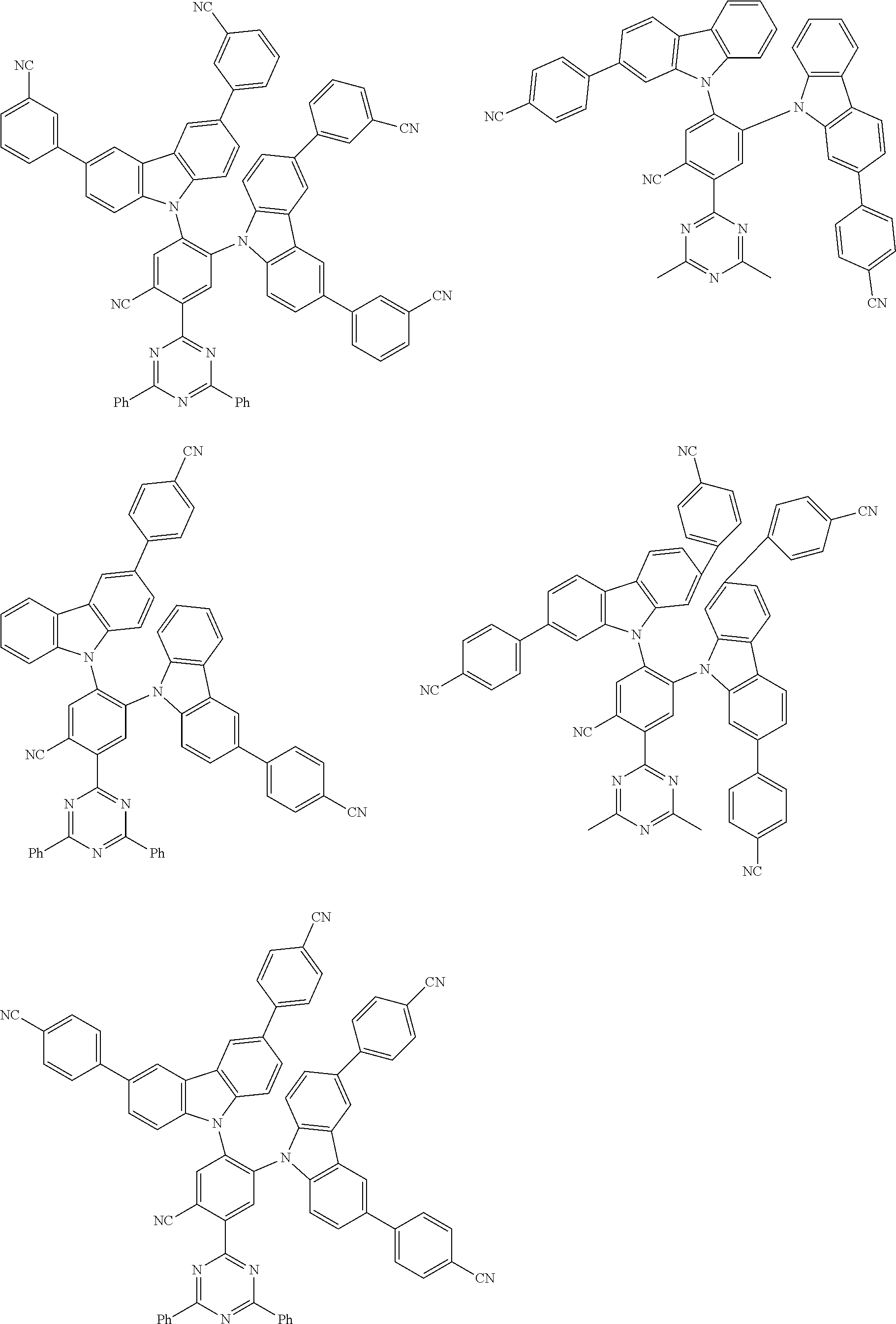


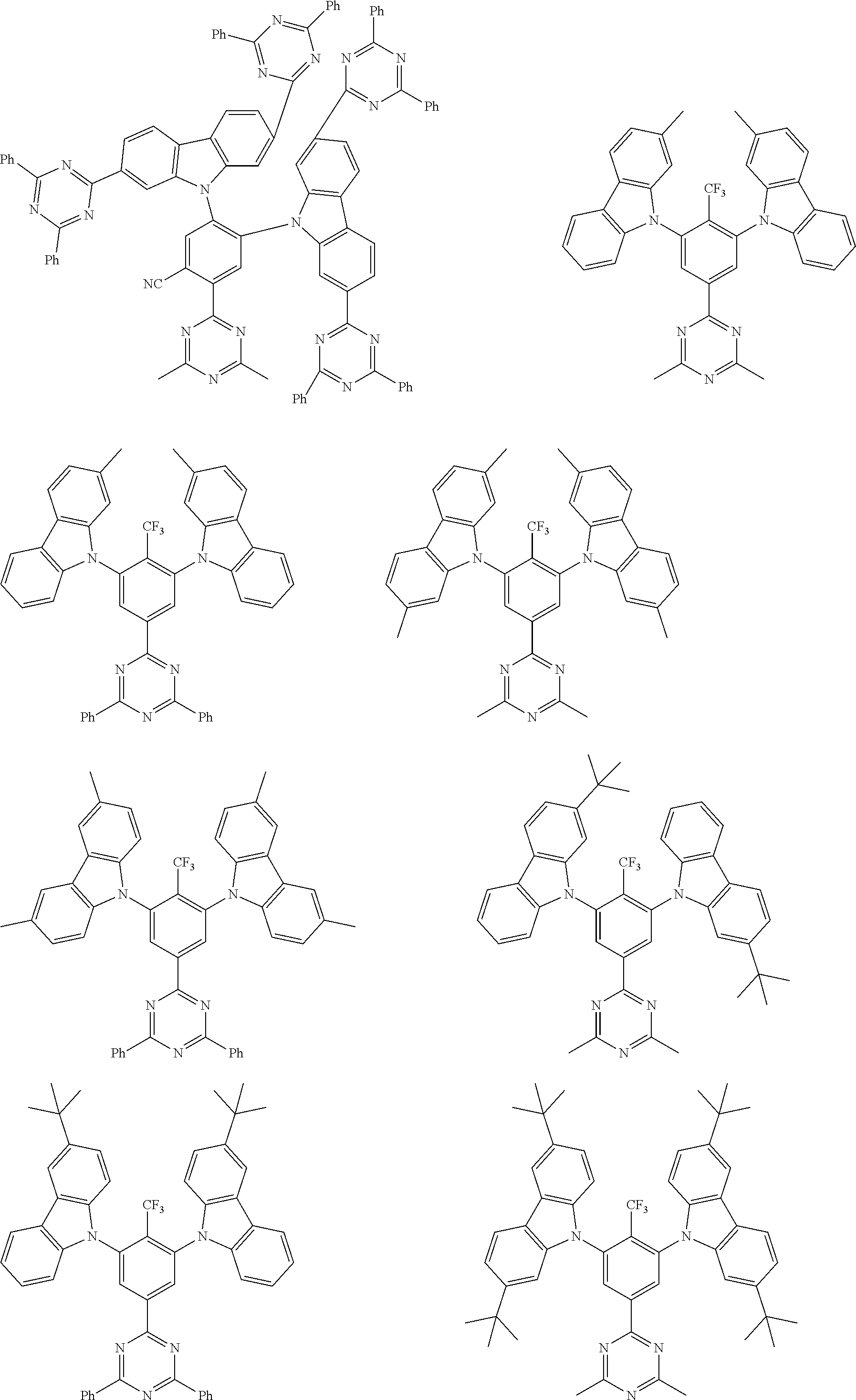


Claims (19)


Applications Claiming Priority (8)
| Application Number | Priority Date | Filing Date | Title |
|---|---|---|---|
| EP16186775 | 2016-09-01 | ||
| EP16186775.9 | 2016-09-01 | ||
| EP16186775 | 2016-09-01 | ||
| DE102016123105.3A DE102016123105B4 (en) | 2016-09-01 | 2016-11-30 | Organic molecules, in particular for use in organic optoelectronic devices |
| DE102016123105.3 | 2016-11-30 | ||
| DE102017105692.0 | 2017-03-16 | ||
| DE102017105692 | 2017-03-16 | ||
| PCT/EP2017/071832 WO2018041933A1 (en) | 2016-09-01 | 2017-08-31 | Organic molecules, especially for use in organic optoelectronic devices |
Publications (2)
| Publication Number | Publication Date |
|---|---|
| US20190194171A1 US20190194171A1 (en) | 2019-06-27 |
| US11492344B2 true US11492344B2 (en) | 2022-11-08 |
Family
ID=61300176
Family Applications (1)
| Application Number | Title | Priority Date | Filing Date |
|---|---|---|---|
| US16/329,052 Active 2039-03-12 US11492344B2 (en) | 2016-09-01 | 2017-08-31 | Organic molecules for use in organic optoelectronic devices |
Country Status (4)
| Country | Link |
|---|---|
| US (1) | US11492344B2 (en) |
| EP (1) | EP3507285B1 (en) |
| CN (1) | CN109641880A (en) |
| WO (1) | WO2018041933A1 (en) |
Families Citing this family (12)
| Publication number | Priority date | Publication date | Assignee | Title |
|---|---|---|---|---|
| EP3511321B1 (en) * | 2016-09-09 | 2021-11-03 | Toyobo Co., Ltd. | Organic light-emitting element, and light-emitting material and compound for use therein |
| JP7165943B2 (en) * | 2017-11-01 | 2022-11-07 | 東洋紡株式会社 | Compounds having a π-electron conjugated unit and a carbazole group |
| EP3540808A1 (en) * | 2018-03-16 | 2019-09-18 | Cynora Gmbh | Organic molecules, in particular for use in optoelectronic devices |
| DE102018107166B4 (en) * | 2018-03-26 | 2020-06-25 | Cynora Gmbh | Organic molecules, especially for use in optoelectronic devices |
| JP7206611B2 (en) * | 2018-03-28 | 2023-01-18 | 三菱ケミカル株式会社 | Composition for luminescent layer of organic electroluminescent device, organic electroluminescent device, display device and lighting |
| KR102222720B1 (en) * | 2018-03-28 | 2021-03-04 | 주식회사 엘지화학 | Compound and organic light emitting device comprising the same |
| JP7412773B2 (en) * | 2018-03-30 | 2024-01-15 | 株式会社Kyulux | Compositions used in organic light emitting diodes |
| KR20190121418A (en) * | 2018-04-17 | 2019-10-28 | 삼성디스플레이 주식회사 | Organic electroluminescence device and nitrogen-containing compound for organic electroluminescence device |
| KR102664158B1 (en) * | 2018-12-24 | 2024-05-08 | 엘지디스플레이 주식회사 | Organic compounds, organic light emitting diode and organic light emitting device haivng the compounds |
| TWI694987B (en) * | 2019-03-26 | 2020-06-01 | 元智大學 | Nitrile compound, the manufacturing method and the use of the same as light emitting materials, and organic light emitting diodes |
| WO2021040467A1 (en) * | 2019-08-28 | 2021-03-04 | 주식회사 엘지화학 | Novel heterocyclic compound and organic light-emitting device using same |
| CN113454078B (en) * | 2019-08-28 | 2023-12-01 | 株式会社Lg化学 | Novel heterocyclic compound and organic light-emitting device comprising same |
Citations (9)
| Publication number | Priority date | Publication date | Assignee | Title |
|---|---|---|---|---|
| WO2014148493A1 (en) | 2013-03-18 | 2014-09-25 | 出光興産株式会社 | Light-emitting device |
| WO2015033894A1 (en) * | 2013-09-04 | 2015-03-12 | 出光興産株式会社 | Carbazole derivative, material for organic electroluminescent element which comprises same, and organic electroluminescent element and electronic device each manufactured using same |
| US20150318488A1 (en) | 2014-05-02 | 2015-11-05 | Samsung Display Co., Ltd. | Organic light-emitting device |
| US20150325801A1 (en) | 2014-05-02 | 2015-11-12 | Samsung Display Co., Ltd. | Organic light-emitting device |
| US20160172601A1 (en) * | 2014-12-12 | 2016-06-16 | Idemitsu Kosan Co., Ltd. | Organic electroluminescent element and electronic device |
| US20190284174A1 (en) * | 2018-03-16 | 2019-09-19 | Cynora Gmbh | Organic molecules for optoelectronic devices |
| US10421746B2 (en) * | 2016-11-01 | 2019-09-24 | Cynora Gmbh | Organic molecules, especially for use in organic optoelectronic devices |
| US20200385399A1 (en) * | 2017-05-04 | 2020-12-10 | Cynora Gmbh | Organic molecules for use in optoelectronic devices |
| US20210155849A1 (en) * | 2018-04-11 | 2021-05-27 | Nanoco Technologies Ltd. | Top-emitting printed display with quantum dots and thermally activated delayed fluorescence molecules |
-
2017
- 2017-08-31 WO PCT/EP2017/071832 patent/WO2018041933A1/en unknown
- 2017-08-31 EP EP17772612.2A patent/EP3507285B1/en active Active
- 2017-08-31 US US16/329,052 patent/US11492344B2/en active Active
- 2017-08-31 CN CN201780053927.3A patent/CN109641880A/en active Pending
Patent Citations (14)
| Publication number | Priority date | Publication date | Assignee | Title |
|---|---|---|---|---|
| WO2014148493A1 (en) | 2013-03-18 | 2014-09-25 | 出光興産株式会社 | Light-emitting device |
| US20160028025A1 (en) | 2013-03-18 | 2016-01-28 | Idemitsu Kosan Co., Ltd. | Light-emitting device |
| US20160204361A1 (en) * | 2013-09-04 | 2016-07-14 | Idemitsu Kosan Co., Ltd. | Carbazole derivative, material for organic electroluminescent element which comprises same, and organic electroluminescent element and electronic device each manufactured using same |
| WO2015033894A1 (en) * | 2013-09-04 | 2015-03-12 | 出光興産株式会社 | Carbazole derivative, material for organic electroluminescent element which comprises same, and organic electroluminescent element and electronic device each manufactured using same |
| US9963429B2 (en) * | 2013-09-04 | 2018-05-08 | Idemitsu Kosan Co., Ltd. | Carbazole derivative, material for organic electroluminescent element which comprises same, and organic electroluminescent element and electronic device each manufactured using same |
| US20150325801A1 (en) | 2014-05-02 | 2015-11-12 | Samsung Display Co., Ltd. | Organic light-emitting device |
| US20150318488A1 (en) | 2014-05-02 | 2015-11-05 | Samsung Display Co., Ltd. | Organic light-emitting device |
| US20160172601A1 (en) * | 2014-12-12 | 2016-06-16 | Idemitsu Kosan Co., Ltd. | Organic electroluminescent element and electronic device |
| US9997717B2 (en) * | 2014-12-12 | 2018-06-12 | Idemitsu Kosan Co., Ltd. | Organic electroluminescence device and electronic device |
| US10421746B2 (en) * | 2016-11-01 | 2019-09-24 | Cynora Gmbh | Organic molecules, especially for use in organic optoelectronic devices |
| US20200385399A1 (en) * | 2017-05-04 | 2020-12-10 | Cynora Gmbh | Organic molecules for use in optoelectronic devices |
| US10981930B2 (en) * | 2017-05-04 | 2021-04-20 | Cynora Gmbh | Organic molecules for use in optoelectronic devices |
| US20190284174A1 (en) * | 2018-03-16 | 2019-09-19 | Cynora Gmbh | Organic molecules for optoelectronic devices |
| US20210155849A1 (en) * | 2018-04-11 | 2021-05-27 | Nanoco Technologies Ltd. | Top-emitting printed display with quantum dots and thermally activated delayed fluorescence molecules |
Also Published As
| Publication number | Publication date |
|---|---|
| CN109641880A (en) | 2019-04-16 |
| WO2018041933A1 (en) | 2018-03-08 |
| EP3507285B1 (en) | 2020-10-21 |
| EP3507285A1 (en) | 2019-07-10 |
| US20190194171A1 (en) | 2019-06-27 |
Similar Documents
| Publication | Publication Date | Title |
|---|---|---|
| US11588114B2 (en) | Organic molecules for use in optoelectronic devices | |
| US10421746B2 (en) | Organic molecules, especially for use in organic optoelectronic devices | |
| US11492344B2 (en) | Organic molecules for use in organic optoelectronic devices | |
| US10439151B2 (en) | Organic molecules, especially for use in organic optoelectronic devices | |
| US11005048B2 (en) | Organic molecules, in particular for use in optoelectronic devices | |
| US20190177303A1 (en) | Organic molecules for use in optoelectronic devices | |
| US20200358002A1 (en) | Organic molecules for use in optoelectronic devices | |
| US11380849B2 (en) | Organic molecules for use in optoelectronic devices | |
| US11825743B2 (en) | Organic molecules for use in organic optoelectronic devices | |
| US11161836B2 (en) | Organic molecules for optoelectronic devices | |
| US20230403931A1 (en) | Organic molecules for optoelectronic devices | |
| US11136294B2 (en) | Organic molecules for use in optoelectronic devices | |
| US11271174B2 (en) | Organic molecules for use in organic optoelectronic devices | |
| US20230167095A1 (en) | Organic molecules for use in optoelectronic devices | |
| US11600783B2 (en) | Organic molecules for use in optoelectronic devices | |
| US10998504B2 (en) | Organic molecules for use in optoelectronic devices | |
| US11597719B2 (en) | Organic molecules for use in organic optoelectronic devices | |
| US11456426B2 (en) | Organic molecules for use in organic optoelectronic devices | |
| US11104645B2 (en) | Organic molecules for use in optoelectronic devices | |
| US11548869B2 (en) | Organic molecules for use in organic optoelectronic devices | |
| US11919882B2 (en) | Organic molecules for use in organic optoelectronic devices | |
| US10971688B2 (en) | Organic molecules for use in organic optoelectronic devices | |
| US11661412B2 (en) | Organic molecules for use in organic optoelectronic devices | |
| US12035623B2 (en) | Organic molecules for optoelectronic devices | |
| US20230389424A1 (en) | Organic molecules for optoelectronic devices |
Legal Events
| Date | Code | Title | Description |
|---|---|---|---|
| FEPP | Fee payment procedure |
Free format text: ENTITY STATUS SET TO UNDISCOUNTED (ORIGINAL EVENT CODE: BIG.); ENTITY STATUS OF PATENT OWNER: LARGE ENTITY |
|
| FEPP | Fee payment procedure |
Free format text: ENTITY STATUS SET TO SMALL (ORIGINAL EVENT CODE: SMAL); ENTITY STATUS OF PATENT OWNER: LARGE ENTITY |
|
| STPP | Information on status: patent application and granting procedure in general |
Free format text: DOCKETED NEW CASE - READY FOR EXAMINATION |
|
| AS | Assignment |
Owner name: CYNORA GMBH, GERMANY Free format text: ASSIGNMENT OF ASSIGNORS INTEREST;ASSIGNORS:BERGMANN, LARISSA;ZINK, DANIEL;SEIFERMANN, STEFAN;SIGNING DATES FROM 20190516 TO 20190611;REEL/FRAME:049434/0174 |
|
| STPP | Information on status: patent application and granting procedure in general |
Free format text: NON FINAL ACTION MAILED |
|
| STPP | Information on status: patent application and granting procedure in general |
Free format text: RESPONSE TO NON-FINAL OFFICE ACTION ENTERED AND FORWARDED TO EXAMINER |
|
| STPP | Information on status: patent application and granting procedure in general |
Free format text: FINAL REJECTION MAILED |
|
| AS | Assignment |
Owner name: SAMSUNG DISPLAY CO., LTD., KOREA, REPUBLIC OF Free format text: ASSIGNMENT OF ASSIGNORS INTEREST;ASSIGNOR:CYNORA GMBH;REEL/FRAME:060329/0712 Effective date: 20220527 |
|
| STPP | Information on status: patent application and granting procedure in general |
Free format text: NOTICE OF ALLOWANCE MAILED -- APPLICATION RECEIVED IN OFFICE OF PUBLICATIONS |
|
| FEPP | Fee payment procedure |
Free format text: ENTITY STATUS SET TO UNDISCOUNTED (ORIGINAL EVENT CODE: BIG.); ENTITY STATUS OF PATENT OWNER: LARGE ENTITY |
|
| STPP | Information on status: patent application and granting procedure in general |
Free format text: PUBLICATIONS -- ISSUE FEE PAYMENT RECEIVED |
|
| STPP | Information on status: patent application and granting procedure in general |
Free format text: PUBLICATIONS -- ISSUE FEE PAYMENT VERIFIED |
|
| STCF | Information on status: patent grant |
Free format text: PATENTED CASE |