US11489125B2 - Organic electroluminescence device and monoamine compound for organic electroluminescence device - Google Patents
Organic electroluminescence device and monoamine compound for organic electroluminescence device Download PDFInfo
- Publication number
- US11489125B2 US11489125B2 US16/403,308 US201916403308A US11489125B2 US 11489125 B2 US11489125 B2 US 11489125B2 US 201916403308 A US201916403308 A US 201916403308A US 11489125 B2 US11489125 B2 US 11489125B2
- Authority
- US
- United States
- Prior art keywords
- formula
- ring
- substituted
- carbon atoms
- group
- Prior art date
- Legal status (The legal status is an assumption and is not a legal conclusion. Google has not performed a legal analysis and makes no representation as to the accuracy of the status listed.)
- Active, expires
Links
- 150000001875 compounds Chemical class 0.000 title claims abstract description 178
- 238000005401 electroluminescence Methods 0.000 title claims abstract description 57
- 125000003003 spiro group Chemical group 0.000 claims abstract description 38
- 239000011368 organic material Substances 0.000 claims abstract description 23
- 239000010410 layer Substances 0.000 claims description 199
- 239000012044 organic layer Substances 0.000 claims description 115
- -1 amine compound Chemical class 0.000 claims description 101
- 230000005525 hole transport Effects 0.000 claims description 88
- 239000000463 material Substances 0.000 claims description 56
- 125000004432 carbon atom Chemical group C* 0.000 claims description 49
- 238000002347 injection Methods 0.000 claims description 32
- 239000007924 injection Substances 0.000 claims description 32
- 229910052799 carbon Inorganic materials 0.000 claims description 27
- 229910052760 oxygen Inorganic materials 0.000 claims description 23
- 229910052717 sulfur Inorganic materials 0.000 claims description 23
- 125000004429 atom Chemical group 0.000 claims description 22
- OKTJSMMVPCPJKN-UHFFFAOYSA-N Carbon Chemical group [C] OKTJSMMVPCPJKN-UHFFFAOYSA-N 0.000 claims description 20
- 125000000623 heterocyclic group Chemical group 0.000 claims description 17
- 229910052710 silicon Inorganic materials 0.000 claims description 17
- 125000003118 aryl group Chemical group 0.000 claims description 15
- 125000000217 alkyl group Chemical group 0.000 claims description 12
- 125000000732 arylene group Chemical group 0.000 claims description 11
- 125000001072 heteroaryl group Chemical group 0.000 claims description 10
- 125000005549 heteroarylene group Chemical group 0.000 claims description 10
- 239000010703 silicon Substances 0.000 claims description 9
- 125000001183 hydrocarbyl group Chemical group 0.000 claims 3
- YXFVVABEGXRONW-UHFFFAOYSA-N Toluene Chemical compound CC1=CC=CC=C1 YXFVVABEGXRONW-UHFFFAOYSA-N 0.000 description 270
- CSNNHWWHGAXBCP-UHFFFAOYSA-L Magnesium sulfate Chemical compound [Mg+2].[O-][S+2]([O-])([O-])[O-] CSNNHWWHGAXBCP-UHFFFAOYSA-L 0.000 description 140
- VLKZOEOYAKHREP-UHFFFAOYSA-N n-Hexane Chemical compound CCCCCC VLKZOEOYAKHREP-UHFFFAOYSA-N 0.000 description 137
- 229910052943 magnesium sulfate Inorganic materials 0.000 description 70
- 239000000243 solution Substances 0.000 description 66
- 230000015572 biosynthetic process Effects 0.000 description 56
- 238000003786 synthesis reaction Methods 0.000 description 56
- 230000000052 comparative effect Effects 0.000 description 51
- 238000003756 stirring Methods 0.000 description 50
- 239000000203 mixture Substances 0.000 description 46
- 238000004992 fast atom bombardment mass spectroscopy Methods 0.000 description 39
- 239000012298 atmosphere Substances 0.000 description 38
- 150000001793 charged compounds Chemical class 0.000 description 38
- 239000012043 crude product Substances 0.000 description 38
- FAPWRFPIFSIZLT-UHFFFAOYSA-M Sodium chloride Chemical compound [Na+].[Cl-] FAPWRFPIFSIZLT-UHFFFAOYSA-M 0.000 description 37
- 239000007795 chemical reaction product Substances 0.000 description 35
- 238000001816 cooling Methods 0.000 description 35
- 238000010898 silica gel chromatography Methods 0.000 description 35
- 239000002904 solvent Substances 0.000 description 35
- UIIMBOGNXHQVGW-UHFFFAOYSA-M Sodium bicarbonate Chemical compound [Na+].OC([O-])=O UIIMBOGNXHQVGW-UHFFFAOYSA-M 0.000 description 26
- XLYOFNOQVPJJNP-UHFFFAOYSA-N water Substances O XLYOFNOQVPJJNP-UHFFFAOYSA-N 0.000 description 23
- RTZKZFJDLAIYFH-UHFFFAOYSA-N Diethyl ether Chemical compound CCOCC RTZKZFJDLAIYFH-UHFFFAOYSA-N 0.000 description 22
- 238000010438 heat treatment Methods 0.000 description 22
- 239000007787 solid Substances 0.000 description 20
- 0 CC.[2*]N([3*])CC.c1ccc2c(c1)Cc1ccccc1[Y]21c2ccccc2Cc2ccccc21 Chemical compound CC.[2*]N([3*])CC.c1ccc2c(c1)Cc1ccccc1[Y]21c2ccccc2Cc2ccccc21 0.000 description 19
- 238000000034 method Methods 0.000 description 19
- 238000010992 reflux Methods 0.000 description 19
- 230000003028 elevating effect Effects 0.000 description 16
- DLEDOFVPSDKWEF-UHFFFAOYSA-N lithium butane Chemical compound [Li+].CCC[CH2-] DLEDOFVPSDKWEF-UHFFFAOYSA-N 0.000 description 16
- MZRVEZGGRBJDDB-UHFFFAOYSA-N n-Butyllithium Substances [Li]CCCC MZRVEZGGRBJDDB-UHFFFAOYSA-N 0.000 description 16
- 125000005842 heteroatom Chemical group 0.000 description 15
- MFRIHAYPQRLWNB-UHFFFAOYSA-N sodium tert-butoxide Chemical compound [Na+].CC(C)(C)[O-] MFRIHAYPQRLWNB-UHFFFAOYSA-N 0.000 description 15
- BWHDROKFUHTORW-UHFFFAOYSA-N tritert-butylphosphane Chemical compound CC(C)(C)P(C(C)(C)C)C(C)(C)C BWHDROKFUHTORW-UHFFFAOYSA-N 0.000 description 15
- 239000002019 doping agent Substances 0.000 description 14
- 235000017557 sodium bicarbonate Nutrition 0.000 description 13
- 229910000030 sodium bicarbonate Inorganic materials 0.000 description 13
- 125000001424 substituent group Chemical group 0.000 description 13
- QTBSBXVTEAMEQO-UHFFFAOYSA-N Acetic acid Chemical compound CC(O)=O QTBSBXVTEAMEQO-UHFFFAOYSA-N 0.000 description 12
- VEXZGXHMUGYJMC-UHFFFAOYSA-N Hydrochloric acid Chemical compound Cl VEXZGXHMUGYJMC-UHFFFAOYSA-N 0.000 description 12
- 239000002356 single layer Substances 0.000 description 12
- LFQSCWFLJHTTHZ-UHFFFAOYSA-N Ethanol Chemical compound CCO LFQSCWFLJHTTHZ-UHFFFAOYSA-N 0.000 description 10
- 125000003277 amino group Chemical group 0.000 description 10
- BWHMMNNQKKPAPP-UHFFFAOYSA-L potassium carbonate Chemical compound [K+].[K+].[O-]C([O-])=O BWHMMNNQKKPAPP-UHFFFAOYSA-L 0.000 description 10
- 229910052751 metal Inorganic materials 0.000 description 9
- 239000002184 metal Substances 0.000 description 9
- XUIMIQQOPSSXEZ-UHFFFAOYSA-N Silicon Chemical compound [Si] XUIMIQQOPSSXEZ-UHFFFAOYSA-N 0.000 description 8
- 230000000903 blocking effect Effects 0.000 description 8
- NLXLAEXVIDQMFP-UHFFFAOYSA-N Ammonia chloride Chemical class [NH4+].[Cl-] NLXLAEXVIDQMFP-UHFFFAOYSA-N 0.000 description 7
- XLOMVQKBTHCTTD-UHFFFAOYSA-N Zinc monoxide Chemical compound [Zn]=O XLOMVQKBTHCTTD-UHFFFAOYSA-N 0.000 description 7
- 239000000872 buffer Substances 0.000 description 7
- KOFLVDBWRHFSAB-UHFFFAOYSA-N 1,2,4,5-tetrahydro-1-(phenylmethyl)-5,9b(1',2')-benzeno-9bh-benz(g)indol-3(3ah)-one Chemical compound C1C(C=2C3=CC=CC=2)C2=CC=CC=C2C23C1C(=O)CN2CC1=CC=CC=C1 KOFLVDBWRHFSAB-UHFFFAOYSA-N 0.000 description 6
- 229910052782 aluminium Inorganic materials 0.000 description 6
- 230000003247 decreasing effect Effects 0.000 description 6
- 230000008034 disappearance Effects 0.000 description 6
- 150000002430 hydrocarbons Chemical group 0.000 description 6
- 238000004519 manufacturing process Methods 0.000 description 6
- 229910052757 nitrogen Inorganic materials 0.000 description 6
- 239000002994 raw material Substances 0.000 description 6
- NFHFRUOZVGFOOS-UHFFFAOYSA-N Pd(PPh3)4 Substances [Pd].C1=CC=CC=C1P(C=1C=CC=CC=1)C1=CC=CC=C1.C1=CC=CC=C1P(C=1C=CC=CC=1)C1=CC=CC=C1.C1=CC=CC=C1P(C=1C=CC=CC=1)C1=CC=CC=C1.C1=CC=CC=C1P(C=1C=CC=CC=1)C1=CC=CC=C1 NFHFRUOZVGFOOS-UHFFFAOYSA-N 0.000 description 5
- 125000001997 phenyl group Chemical group [H]C1=C([H])C([H])=C(*)C([H])=C1[H] 0.000 description 5
- 229920000767 polyaniline Polymers 0.000 description 5
- 229910000027 potassium carbonate Inorganic materials 0.000 description 5
- ATTVYRDSOVWELU-UHFFFAOYSA-N 1-diphenylphosphoryl-2-(2-diphenylphosphorylphenoxy)benzene Chemical compound C=1C=CC=CC=1P(C=1C(=CC=CC=1)OC=1C(=CC=CC=1)P(=O)(C=1C=CC=CC=1)C=1C=CC=CC=1)(=O)C1=CC=CC=C1 ATTVYRDSOVWELU-UHFFFAOYSA-N 0.000 description 4
- AWXGSYPUMWKTBR-UHFFFAOYSA-N 4-carbazol-9-yl-n,n-bis(4-carbazol-9-ylphenyl)aniline Chemical compound C12=CC=CC=C2C2=CC=CC=C2N1C1=CC=C(N(C=2C=CC(=CC=2)N2C3=CC=CC=C3C3=CC=CC=C32)C=2C=CC(=CC=2)N2C3=CC=CC=C3C3=CC=CC=C32)C=C1 AWXGSYPUMWKTBR-UHFFFAOYSA-N 0.000 description 4
- VFUDMQLBKNMONU-UHFFFAOYSA-N 9-[4-(4-carbazol-9-ylphenyl)phenyl]carbazole Chemical group C12=CC=CC=C2C2=CC=CC=C2N1C1=CC=C(C=2C=CC(=CC=2)N2C3=CC=CC=C3C3=CC=CC=C32)C=C1 VFUDMQLBKNMONU-UHFFFAOYSA-N 0.000 description 4
- MQDMZXOMHAZXSD-UHFFFAOYSA-N CC1(C)c2ccccc2N(c2ccc3c(c2)[Si]2(c4ccccc4Oc4ccccc42)c2ccccc2-3)c2ccccc21.c1ccc2c(c1)Oc1ccccc1N2c1ccc2c(c1)[Si]1(c3ccccc3Oc3ccccc31)c1ccccc1-2.c1ccc2c(c1)Oc1ccccc1[Si]21c2ccccc2-c2ccc(-n3c4ccccc4c4ccccc43)cc21.c1ccc2c(c1)Oc1ccccc1[Si]21c2ccccc2-c2ccc(N3c4ccccc4Sc4ccccc43)cc21 Chemical compound CC1(C)c2ccccc2N(c2ccc3c(c2)[Si]2(c4ccccc4Oc4ccccc42)c2ccccc2-3)c2ccccc21.c1ccc2c(c1)Oc1ccccc1N2c1ccc2c(c1)[Si]1(c3ccccc3Oc3ccccc31)c1ccccc1-2.c1ccc2c(c1)Oc1ccccc1[Si]21c2ccccc2-c2ccc(-n3c4ccccc4c4ccccc43)cc21.c1ccc2c(c1)Oc1ccccc1[Si]21c2ccccc2-c2ccc(N3c4ccccc4Sc4ccccc43)cc21 MQDMZXOMHAZXSD-UHFFFAOYSA-N 0.000 description 4
- 125000003342 alkenyl group Chemical group 0.000 description 4
- PAJKTYGYUKSORL-UHFFFAOYSA-N c1ccc(-c2cc(-c3ccccc3)cc(N(c3ccccc3)c3ccc4c(c3)-c3ccccc3[Si]43c4ccccc4Oc4ccccc43)c2)cc1.c1ccc(-c2ccc(N(c3ccc4c(c3)-c3ccccc3[Si]43c4ccccc4Oc4ccccc43)c3cccc4ccccc34)cc2)cc1.c1ccc(-c2ccc(N(c3ccccc3)c3ccc4c(c3)-c3ccccc3[Si]43c4ccccc4Oc4ccccc43)cc2-c2ccccc2)cc1.c1ccc(-c2ccccc2N(c2ccc(-c3cccc4ccccc34)cc2)c2ccc3c(c2)-c2ccccc2[Si]32c3ccccc3Oc3ccccc32)cc1 Chemical compound c1ccc(-c2cc(-c3ccccc3)cc(N(c3ccccc3)c3ccc4c(c3)-c3ccccc3[Si]43c4ccccc4Oc4ccccc43)c2)cc1.c1ccc(-c2ccc(N(c3ccc4c(c3)-c3ccccc3[Si]43c4ccccc4Oc4ccccc43)c3cccc4ccccc34)cc2)cc1.c1ccc(-c2ccc(N(c3ccccc3)c3ccc4c(c3)-c3ccccc3[Si]43c4ccccc4Oc4ccccc43)cc2-c2ccccc2)cc1.c1ccc(-c2ccccc2N(c2ccc(-c3cccc4ccccc34)cc2)c2ccc3c(c2)-c2ccccc2[Si]32c3ccccc3Oc3ccccc32)cc1 PAJKTYGYUKSORL-UHFFFAOYSA-N 0.000 description 4
- DURKYMOWDZMZDL-UHFFFAOYSA-N c1ccc(-c2cc(-c3ccccc3)cc(N(c3ccccc3)c3ccc4c(c3)Oc3ccccc3[Si]43c4ccccc4-c4ccccc43)c2)cc1.c1ccc(-c2ccc(N(c3ccc4c(c3)Oc3ccccc3[Si]43c4ccccc4-c4ccccc43)c3cccc4ccccc34)cc2)cc1.c1ccc(-c2ccc(N(c3ccccc3)c3ccc4c(c3)Oc3ccccc3[Si]43c4ccccc4-c4ccccc43)cc2-c2ccccc2)cc1.c1ccc(-c2ccccc2N(c2ccc(-c3cccc4ccccc34)cc2)c2ccc3c(c2)Oc2ccccc2[Si]32c3ccccc3-c3ccccc32)cc1 Chemical compound c1ccc(-c2cc(-c3ccccc3)cc(N(c3ccccc3)c3ccc4c(c3)Oc3ccccc3[Si]43c4ccccc4-c4ccccc43)c2)cc1.c1ccc(-c2ccc(N(c3ccc4c(c3)Oc3ccccc3[Si]43c4ccccc4-c4ccccc43)c3cccc4ccccc34)cc2)cc1.c1ccc(-c2ccc(N(c3ccccc3)c3ccc4c(c3)Oc3ccccc3[Si]43c4ccccc4-c4ccccc43)cc2-c2ccccc2)cc1.c1ccc(-c2ccccc2N(c2ccc(-c3cccc4ccccc34)cc2)c2ccc3c(c2)Oc2ccccc2[Si]32c3ccccc3-c3ccccc32)cc1 DURKYMOWDZMZDL-UHFFFAOYSA-N 0.000 description 4
- KNTKFCIEAWWXGA-UHFFFAOYSA-N c1ccc(-c2cc(-c3ccccc3)cc(N(c3ccccc3)c3ccc4c(c3)Oc3ccccc3[Si]43c4ccccc4[Si](c4ccccc4)(c4ccccc4)c4ccccc43)c2)cc1.c1ccc(-c2ccc(N(c3ccc4c(c3)Oc3ccccc3[Si]43c4ccccc4[Si](c4ccccc4)(c4ccccc4)c4ccccc43)c3cccc4ccccc34)cc2)cc1.c1ccc(-c2ccc(N(c3ccccc3)c3ccc4c(c3)Oc3ccccc3[Si]43c4ccccc4[Si](c4ccccc4)(c4ccccc4)c4ccccc43)cc2-c2ccccc2)cc1.c1ccc(-c2ccccc2N(c2ccc(-c3cccc4ccccc34)cc2)c2ccc3c(c2)Oc2ccccc2[Si]32c3ccccc3[Si](c3ccccc3)(c3ccccc3)c3ccccc32)cc1 Chemical compound c1ccc(-c2cc(-c3ccccc3)cc(N(c3ccccc3)c3ccc4c(c3)Oc3ccccc3[Si]43c4ccccc4[Si](c4ccccc4)(c4ccccc4)c4ccccc43)c2)cc1.c1ccc(-c2ccc(N(c3ccc4c(c3)Oc3ccccc3[Si]43c4ccccc4[Si](c4ccccc4)(c4ccccc4)c4ccccc43)c3cccc4ccccc34)cc2)cc1.c1ccc(-c2ccc(N(c3ccccc3)c3ccc4c(c3)Oc3ccccc3[Si]43c4ccccc4[Si](c4ccccc4)(c4ccccc4)c4ccccc43)cc2-c2ccccc2)cc1.c1ccc(-c2ccccc2N(c2ccc(-c3cccc4ccccc34)cc2)c2ccc3c(c2)Oc2ccccc2[Si]32c3ccccc3[Si](c3ccccc3)(c3ccccc3)c3ccccc32)cc1 KNTKFCIEAWWXGA-UHFFFAOYSA-N 0.000 description 4
- NBRZSEKMJLGBQW-UHFFFAOYSA-N c1ccc(-c2cc(-c3ccccc3)cc(N(c3ccccc3)c3ccc4c(c3)Sc3ccccc3[Si]43c4ccccc4-c4ccccc43)c2)cc1.c1ccc(-c2ccc(N(c3ccc4c(c3)Sc3ccccc3[Si]43c4ccccc4-c4ccccc43)c3cccc4ccccc34)cc2)cc1.c1ccc(-c2ccc(N(c3ccccc3)c3ccc4c(c3)Sc3ccccc3[Si]43c4ccccc4-c4ccccc43)cc2-c2ccccc2)cc1.c1ccc(-c2ccccc2N(c2ccc(-c3cccc4ccccc34)cc2)c2ccc3c(c2)Sc2ccccc2[Si]32c3ccccc3-c3ccccc32)cc1 Chemical compound c1ccc(-c2cc(-c3ccccc3)cc(N(c3ccccc3)c3ccc4c(c3)Sc3ccccc3[Si]43c4ccccc4-c4ccccc43)c2)cc1.c1ccc(-c2ccc(N(c3ccc4c(c3)Sc3ccccc3[Si]43c4ccccc4-c4ccccc43)c3cccc4ccccc34)cc2)cc1.c1ccc(-c2ccc(N(c3ccccc3)c3ccc4c(c3)Sc3ccccc3[Si]43c4ccccc4-c4ccccc43)cc2-c2ccccc2)cc1.c1ccc(-c2ccccc2N(c2ccc(-c3cccc4ccccc34)cc2)c2ccc3c(c2)Sc2ccccc2[Si]32c3ccccc3-c3ccccc32)cc1 NBRZSEKMJLGBQW-UHFFFAOYSA-N 0.000 description 4
- HGIUKBZUVFEEEL-UHFFFAOYSA-N c1ccc(-c2cc(-c3ccccc3)cc(N(c3ccccc3)c3ccc4c(c3)Sc3ccccc3[Si]43c4ccccc4Oc4ccccc43)c2)cc1.c1ccc(-c2ccc(N(c3ccc4c(c3)Sc3ccccc3[Si]43c4ccccc4Oc4ccccc43)c3cccc4ccccc34)cc2)cc1.c1ccc(-c2ccc(N(c3ccccc3)c3ccc4c(c3)Sc3ccccc3[Si]43c4ccccc4Oc4ccccc43)cc2-c2ccccc2)cc1.c1ccc(-c2ccccc2N(c2ccc(-c3cccc4ccccc34)cc2)c2ccc3c(c2)Sc2ccccc2[Si]32c3ccccc3Oc3ccccc32)cc1 Chemical compound c1ccc(-c2cc(-c3ccccc3)cc(N(c3ccccc3)c3ccc4c(c3)Sc3ccccc3[Si]43c4ccccc4Oc4ccccc43)c2)cc1.c1ccc(-c2ccc(N(c3ccc4c(c3)Sc3ccccc3[Si]43c4ccccc4Oc4ccccc43)c3cccc4ccccc34)cc2)cc1.c1ccc(-c2ccc(N(c3ccccc3)c3ccc4c(c3)Sc3ccccc3[Si]43c4ccccc4Oc4ccccc43)cc2-c2ccccc2)cc1.c1ccc(-c2ccccc2N(c2ccc(-c3cccc4ccccc34)cc2)c2ccc3c(c2)Sc2ccccc2[Si]32c3ccccc3Oc3ccccc32)cc1 HGIUKBZUVFEEEL-UHFFFAOYSA-N 0.000 description 4
- YJLHTQWKCORYIH-UHFFFAOYSA-N c1ccc(-c2cc(-c3ccccc3)cc(N(c3ccccc3)c3ccc4c(c3)Sc3ccccc3[Si]43c4ccccc4Sc4ccccc43)c2)cc1.c1ccc(-c2ccc(N(c3ccc4c(c3)Sc3ccccc3[Si]43c4ccccc4Sc4ccccc43)c3cccc4ccccc34)cc2)cc1.c1ccc(-c2ccc(N(c3ccccc3)c3ccc4c(c3)Sc3ccccc3[Si]43c4ccccc4Sc4ccccc43)cc2-c2ccccc2)cc1.c1ccc(-c2ccccc2N(c2ccc(-c3cccc4ccccc34)cc2)c2ccc3c(c2)Sc2ccccc2[Si]32c3ccccc3Sc3ccccc32)cc1 Chemical compound c1ccc(-c2cc(-c3ccccc3)cc(N(c3ccccc3)c3ccc4c(c3)Sc3ccccc3[Si]43c4ccccc4Sc4ccccc43)c2)cc1.c1ccc(-c2ccc(N(c3ccc4c(c3)Sc3ccccc3[Si]43c4ccccc4Sc4ccccc43)c3cccc4ccccc34)cc2)cc1.c1ccc(-c2ccc(N(c3ccccc3)c3ccc4c(c3)Sc3ccccc3[Si]43c4ccccc4Sc4ccccc43)cc2-c2ccccc2)cc1.c1ccc(-c2ccccc2N(c2ccc(-c3cccc4ccccc34)cc2)c2ccc3c(c2)Sc2ccccc2[Si]32c3ccccc3Sc3ccccc32)cc1 YJLHTQWKCORYIH-UHFFFAOYSA-N 0.000 description 4
- MMXFIFVSABJIGG-UHFFFAOYSA-N c1ccc(N(c2ccc3c(c2)Oc2ccccc2[Si]32c3ccccc3-c3ccccc32)c2ccc3c(c2)C(c2ccccc2)(c2ccccc2)c2ccccc2-3)cc1.c1ccc(N(c2ccc3c(c2)Oc2ccccc2[Si]32c3ccccc3-c3ccccc32)c2cccc3c2-c2ccccc2C3(c2ccccc2)c2ccccc2)cc1.c1ccc2c(c1)Oc1cc(N(c3ccc(-c4cccc5ccccc45)cc3)c3cccc4c3sc3ccccc34)ccc1[Si]21c2ccccc2-c2ccccc21.c1ccc2c(c1)Oc1cc(N(c3ccc4c(c3)oc3ccccc34)c3ccc4c(c3)oc3ccccc34)ccc1[Si]21c2ccccc2-c2ccccc21 Chemical compound c1ccc(N(c2ccc3c(c2)Oc2ccccc2[Si]32c3ccccc3-c3ccccc32)c2ccc3c(c2)C(c2ccccc2)(c2ccccc2)c2ccccc2-3)cc1.c1ccc(N(c2ccc3c(c2)Oc2ccccc2[Si]32c3ccccc3-c3ccccc32)c2cccc3c2-c2ccccc2C3(c2ccccc2)c2ccccc2)cc1.c1ccc2c(c1)Oc1cc(N(c3ccc(-c4cccc5ccccc45)cc3)c3cccc4c3sc3ccccc34)ccc1[Si]21c2ccccc2-c2ccccc21.c1ccc2c(c1)Oc1cc(N(c3ccc4c(c3)oc3ccccc34)c3ccc4c(c3)oc3ccccc34)ccc1[Si]21c2ccccc2-c2ccccc21 MMXFIFVSABJIGG-UHFFFAOYSA-N 0.000 description 4
- BIBMLRQIFGMMKU-UHFFFAOYSA-N c1ccc(N(c2ccc3c(c2)Oc2ccccc2[Si]32c3ccccc3[Si](c3ccccc3)(c3ccccc3)c3ccccc32)c2ccc3c(c2)C(c2ccccc2)(c2ccccc2)c2ccccc2-3)cc1.c1ccc(N(c2ccc3c(c2)Oc2ccccc2[Si]32c3ccccc3[Si](c3ccccc3)(c3ccccc3)c3ccccc32)c2cccc3c2-c2ccccc2C3(c2ccccc2)c2ccccc2)cc1.c1ccc([Si]2(c3ccccc3)c3ccccc3[Si]3(c4ccccc4Oc4cc(N(c5ccc(-c6cccc7ccccc67)cc5)c5cccc6c5sc5ccccc56)ccc43)c3ccccc32)cc1.c1ccc([Si]2(c3ccccc3)c3ccccc3[Si]3(c4ccccc4Oc4cc(N(c5ccc6c(c5)oc5ccccc56)c5ccc6c(c5)oc5ccccc56)ccc43)c3ccccc32)cc1 Chemical compound c1ccc(N(c2ccc3c(c2)Oc2ccccc2[Si]32c3ccccc3[Si](c3ccccc3)(c3ccccc3)c3ccccc32)c2ccc3c(c2)C(c2ccccc2)(c2ccccc2)c2ccccc2-3)cc1.c1ccc(N(c2ccc3c(c2)Oc2ccccc2[Si]32c3ccccc3[Si](c3ccccc3)(c3ccccc3)c3ccccc32)c2cccc3c2-c2ccccc2C3(c2ccccc2)c2ccccc2)cc1.c1ccc([Si]2(c3ccccc3)c3ccccc3[Si]3(c4ccccc4Oc4cc(N(c5ccc(-c6cccc7ccccc67)cc5)c5cccc6c5sc5ccccc56)ccc43)c3ccccc32)cc1.c1ccc([Si]2(c3ccccc3)c3ccccc3[Si]3(c4ccccc4Oc4cc(N(c5ccc6c(c5)oc5ccccc56)c5ccc6c(c5)oc5ccccc56)ccc43)c3ccccc32)cc1 BIBMLRQIFGMMKU-UHFFFAOYSA-N 0.000 description 4
- SDBGTAJRUJLHQT-UHFFFAOYSA-N c1ccc(N(c2ccc3c(c2)Sc2ccccc2[Si]32c3ccccc3-c3ccccc32)c2ccc3c(c2)C(c2ccccc2)(c2ccccc2)c2ccccc2-3)cc1.c1ccc(N(c2ccc3c(c2)Sc2ccccc2[Si]32c3ccccc3-c3ccccc32)c2cccc3c2-c2ccccc2C3(c2ccccc2)c2ccccc2)cc1.c1ccc2c(c1)Sc1cc(N(c3ccc(-c4cccc5ccccc45)cc3)c3cccc4c3sc3ccccc34)ccc1[Si]21c2ccccc2-c2ccccc21.c1ccc2c(c1)Sc1cc(N(c3ccc4c(c3)oc3ccccc34)c3ccc4c(c3)oc3ccccc34)ccc1[Si]21c2ccccc2-c2ccccc21 Chemical compound c1ccc(N(c2ccc3c(c2)Sc2ccccc2[Si]32c3ccccc3-c3ccccc32)c2ccc3c(c2)C(c2ccccc2)(c2ccccc2)c2ccccc2-3)cc1.c1ccc(N(c2ccc3c(c2)Sc2ccccc2[Si]32c3ccccc3-c3ccccc32)c2cccc3c2-c2ccccc2C3(c2ccccc2)c2ccccc2)cc1.c1ccc2c(c1)Sc1cc(N(c3ccc(-c4cccc5ccccc45)cc3)c3cccc4c3sc3ccccc34)ccc1[Si]21c2ccccc2-c2ccccc21.c1ccc2c(c1)Sc1cc(N(c3ccc4c(c3)oc3ccccc34)c3ccc4c(c3)oc3ccccc34)ccc1[Si]21c2ccccc2-c2ccccc21 SDBGTAJRUJLHQT-UHFFFAOYSA-N 0.000 description 4
- LBFSKBGOVSFPAU-UHFFFAOYSA-N c1ccc(N(c2ccc3c(c2)Sc2ccccc2[Si]32c3ccccc3Oc3ccccc32)c2ccc3c(c2)C(c2ccccc2)(c2ccccc2)c2ccccc2-3)cc1.c1ccc(N(c2ccc3c(c2)Sc2ccccc2[Si]32c3ccccc3Oc3ccccc32)c2cccc3c2-c2ccccc2C3(c2ccccc2)c2ccccc2)cc1.c1ccc2c(c1)Oc1ccccc1[Si]21c2ccccc2Sc2cc(N(c3ccc(-c4cccc5ccccc45)cc3)c3cccc4c3sc3ccccc34)ccc21.c1ccc2c(c1)Oc1ccccc1[Si]21c2ccccc2Sc2cc(N(c3ccc4c(c3)oc3ccccc34)c3ccc4c(c3)oc3ccccc34)ccc21 Chemical compound c1ccc(N(c2ccc3c(c2)Sc2ccccc2[Si]32c3ccccc3Oc3ccccc32)c2ccc3c(c2)C(c2ccccc2)(c2ccccc2)c2ccccc2-3)cc1.c1ccc(N(c2ccc3c(c2)Sc2ccccc2[Si]32c3ccccc3Oc3ccccc32)c2cccc3c2-c2ccccc2C3(c2ccccc2)c2ccccc2)cc1.c1ccc2c(c1)Oc1ccccc1[Si]21c2ccccc2Sc2cc(N(c3ccc(-c4cccc5ccccc45)cc3)c3cccc4c3sc3ccccc34)ccc21.c1ccc2c(c1)Oc1ccccc1[Si]21c2ccccc2Sc2cc(N(c3ccc4c(c3)oc3ccccc34)c3ccc4c(c3)oc3ccccc34)ccc21 LBFSKBGOVSFPAU-UHFFFAOYSA-N 0.000 description 4
- QHCGSDAAWJCNRY-UHFFFAOYSA-N c1ccc(N(c2ccc3c(c2)Sc2ccccc2[Si]32c3ccccc3Sc3ccccc32)c2ccc3c(c2)C(c2ccccc2)(c2ccccc2)c2ccccc2-3)cc1.c1ccc(N(c2ccc3c(c2)Sc2ccccc2[Si]32c3ccccc3Sc3ccccc32)c2cccc3c2-c2ccccc2C3(c2ccccc2)c2ccccc2)cc1.c1ccc2c(c1)Sc1ccccc1[Si]21c2ccccc2Sc2cc(N(c3ccc(-c4cccc5ccccc45)cc3)c3cccc4c3sc3ccccc34)ccc21.c1ccc2c(c1)Sc1ccccc1[Si]21c2ccccc2Sc2cc(N(c3ccc4c(c3)oc3ccccc34)c3ccc4c(c3)oc3ccccc34)ccc21 Chemical compound c1ccc(N(c2ccc3c(c2)Sc2ccccc2[Si]32c3ccccc3Sc3ccccc32)c2ccc3c(c2)C(c2ccccc2)(c2ccccc2)c2ccccc2-3)cc1.c1ccc(N(c2ccc3c(c2)Sc2ccccc2[Si]32c3ccccc3Sc3ccccc32)c2cccc3c2-c2ccccc2C3(c2ccccc2)c2ccccc2)cc1.c1ccc2c(c1)Sc1ccccc1[Si]21c2ccccc2Sc2cc(N(c3ccc(-c4cccc5ccccc45)cc3)c3cccc4c3sc3ccccc34)ccc21.c1ccc2c(c1)Sc1ccccc1[Si]21c2ccccc2Sc2cc(N(c3ccc4c(c3)oc3ccccc34)c3ccc4c(c3)oc3ccccc34)ccc21 QHCGSDAAWJCNRY-UHFFFAOYSA-N 0.000 description 4
- 238000006243 chemical reaction Methods 0.000 description 4
- TXCDCPKCNAJMEE-UHFFFAOYSA-N dibenzofuran Chemical compound C1=CC=C2C3=CC=CC=C3OC2=C1 TXCDCPKCNAJMEE-UHFFFAOYSA-N 0.000 description 4
- 229910052749 magnesium Inorganic materials 0.000 description 4
- 229910044991 metal oxide Inorganic materials 0.000 description 4
- 150000004706 metal oxides Chemical class 0.000 description 4
- 229910052709 silver Inorganic materials 0.000 description 4
- BATOISXASQUNHX-UHFFFAOYSA-N 1-bromo-2-phenylsulfanylbenzene Chemical compound BrC1=CC=CC=C1SC1=CC=CC=C1 BATOISXASQUNHX-UHFFFAOYSA-N 0.000 description 3
- GEQBRULPNIVQPP-UHFFFAOYSA-N 2-[3,5-bis(1-phenylbenzimidazol-2-yl)phenyl]-1-phenylbenzimidazole Chemical compound C1=CC=CC=C1N1C2=CC=CC=C2N=C1C1=CC(C=2N(C3=CC=CC=C3N=2)C=2C=CC=CC=2)=CC(C=2N(C3=CC=CC=C3N=2)C=2C=CC=CC=2)=C1 GEQBRULPNIVQPP-UHFFFAOYSA-N 0.000 description 3
- VIZUPBYFLORCRA-UHFFFAOYSA-N 9,10-dinaphthalen-2-ylanthracene Chemical compound C12=CC=CC=C2C(C2=CC3=CC=CC=C3C=C2)=C(C=CC=C2)C2=C1C1=CC=C(C=CC=C2)C2=C1 VIZUPBYFLORCRA-UHFFFAOYSA-N 0.000 description 3
- RAPHUPWIHDYTKU-WXUKJITCSA-N 9-ethyl-3-[(e)-2-[4-[4-[(e)-2-(9-ethylcarbazol-3-yl)ethenyl]phenyl]phenyl]ethenyl]carbazole Chemical group C1=CC=C2C3=CC(/C=C/C4=CC=C(C=C4)C4=CC=C(C=C4)/C=C/C=4C=C5C6=CC=CC=C6N(C5=CC=4)CC)=CC=C3N(CC)C2=C1 RAPHUPWIHDYTKU-WXUKJITCSA-N 0.000 description 3
- ATEJRADYHHGLFX-UHFFFAOYSA-N CC.CC.CC.CC.CC.CC.CC.CC.c1ccc(-c2ccccc2)cc1.c1ccc2c(c1)oc1ccccc12.c1ccc2ccccc2c1.c1ccccc1 Chemical compound CC.CC.CC.CC.CC.CC.CC.CC.c1ccc(-c2ccccc2)cc1.c1ccc2c(c1)oc1ccccc12.c1ccc2ccccc2c1.c1ccccc1 ATEJRADYHHGLFX-UHFFFAOYSA-N 0.000 description 3
- XUMDCYBFXNSRRW-UHFFFAOYSA-N CC1(C)c2ccccc2-c2ccc(N(c3ccc(-c4ccccc4)cc3)c3ccc4c(c3)Oc3ccccc3[Si]43c4ccc5c(oc6ccccc65)c4Oc4c3ccc3c4oc4ccccc43)cc21.c1ccc(-c2ccc(N(c3ccc(-c4ccccc4)cc3)c3ccc4c(c3)Oc3ccccc3[Si]43c4ccc5ccccc5c4Oc4c3ccc3ccccc43)cc2)cc1.c1ccc(-c2ccc(N(c3ccc4c(c3)Oc3ccccc3[Si]43c4cc5ccccc5cc4Oc4cc5ccccc5cc43)c3cccc4c3sc3ccccc34)cc2)cc1 Chemical compound CC1(C)c2ccccc2-c2ccc(N(c3ccc(-c4ccccc4)cc3)c3ccc4c(c3)Oc3ccccc3[Si]43c4ccc5c(oc6ccccc65)c4Oc4c3ccc3c4oc4ccccc43)cc21.c1ccc(-c2ccc(N(c3ccc(-c4ccccc4)cc3)c3ccc4c(c3)Oc3ccccc3[Si]43c4ccc5ccccc5c4Oc4c3ccc3ccccc43)cc2)cc1.c1ccc(-c2ccc(N(c3ccc4c(c3)Oc3ccccc3[Si]43c4cc5ccccc5cc4Oc4cc5ccccc5cc43)c3cccc4c3sc3ccccc34)cc2)cc1 XUMDCYBFXNSRRW-UHFFFAOYSA-N 0.000 description 3
- KFZMGEQAYNKOFK-UHFFFAOYSA-N Isopropanol Chemical compound CC(C)O KFZMGEQAYNKOFK-UHFFFAOYSA-N 0.000 description 3
- 229910003910 SiCl4 Inorganic materials 0.000 description 3
- 239000012300 argon atmosphere Substances 0.000 description 3
- 239000004305 biphenyl Substances 0.000 description 3
- MZSNWGZDQSYJJL-UHFFFAOYSA-N c1ccc(-c2cc(-c3ccccc3)cc(N(c3ccccc3)c3ccc4c(c3)-c3ccccc3[Si]43c4ccccc4Sc4ccccc43)c2)cc1.c1ccc(-c2ccc(N(c3ccc4c(c3)-c3ccccc3[Si]43c4ccccc4Sc4ccccc43)c3cccc4ccccc34)cc2)cc1.c1ccc(-c2ccc(N(c3ccccc3)c3ccc4c(c3)-c3ccccc3[Si]43c4ccccc4Sc4ccccc43)cc2-c2ccccc2)cc1.c1ccc(-c2ccccc2N(c2ccc(-c3cccc4ccccc34)cc2)c2ccc3c(c2)-c2ccccc2[Si]32c3ccccc3Sc3ccccc32)cc1 Chemical compound c1ccc(-c2cc(-c3ccccc3)cc(N(c3ccccc3)c3ccc4c(c3)-c3ccccc3[Si]43c4ccccc4Sc4ccccc43)c2)cc1.c1ccc(-c2ccc(N(c3ccc4c(c3)-c3ccccc3[Si]43c4ccccc4Sc4ccccc43)c3cccc4ccccc34)cc2)cc1.c1ccc(-c2ccc(N(c3ccccc3)c3ccc4c(c3)-c3ccccc3[Si]43c4ccccc4Sc4ccccc43)cc2-c2ccccc2)cc1.c1ccc(-c2ccccc2N(c2ccc(-c3cccc4ccccc34)cc2)c2ccc3c(c2)-c2ccccc2[Si]32c3ccccc3Sc3ccccc32)cc1 MZSNWGZDQSYJJL-UHFFFAOYSA-N 0.000 description 3
- WSSFQQILQBJASQ-UHFFFAOYSA-N c1ccc(-c2ccc(N(c3ccc(-c4ccccc4)cc3)c3ccc4c(c3)[Si]3(c5ccccc5O4)c4ccccc4-c4ccccc43)cc2)cc1.c1ccc(-c2ccc(N(c3ccc4c(c3)[Si]3(c5ccccc5O4)c4ccccc4-c4ccccc43)c3ccc4c(ccc5ccccc54)c3)cc2)cc1.c1ccc(-c2ccc(N(c3ccc4c(c3)[Si]3(c5ccccc5O4)c4ccccc4-c4ccccc43)c3cccc4ccccc34)cc2)cc1.c1ccc(-c2ccc3c(c2)oc2cc(N(c4ccccc4)c4ccc5c(c4)[Si]4(c6ccccc6O5)c5ccccc5-c5ccccc54)ccc23)cc1 Chemical compound c1ccc(-c2ccc(N(c3ccc(-c4ccccc4)cc3)c3ccc4c(c3)[Si]3(c5ccccc5O4)c4ccccc4-c4ccccc43)cc2)cc1.c1ccc(-c2ccc(N(c3ccc4c(c3)[Si]3(c5ccccc5O4)c4ccccc4-c4ccccc43)c3ccc4c(ccc5ccccc54)c3)cc2)cc1.c1ccc(-c2ccc(N(c3ccc4c(c3)[Si]3(c5ccccc5O4)c4ccccc4-c4ccccc43)c3cccc4ccccc34)cc2)cc1.c1ccc(-c2ccc3c(c2)oc2cc(N(c4ccccc4)c4ccc5c(c4)[Si]4(c6ccccc6O5)c5ccccc5-c5ccccc54)ccc23)cc1 WSSFQQILQBJASQ-UHFFFAOYSA-N 0.000 description 3
- VWYOOFXSYNZCDV-UHFFFAOYSA-N c1ccc(C2(c3ccccc3)c3ccccc3-c3c(N(c4cccc(-c5ccc6c(c5)[Si]5(c7ccccc7Oc7ccccc75)c5cc7ccccc7cc5O6)c4)c4cccc5ccccc45)cccc32)cc1 Chemical compound c1ccc(C2(c3ccccc3)c3ccccc3-c3c(N(c4cccc(-c5ccc6c(c5)[Si]5(c7ccccc7Oc7ccccc75)c5cc7ccccc7cc5O6)c4)c4cccc5ccccc45)cccc32)cc1 VWYOOFXSYNZCDV-UHFFFAOYSA-N 0.000 description 3
- 230000021615 conjugation Effects 0.000 description 3
- ZUOUZKKEUPVFJK-UHFFFAOYSA-N diphenyl Chemical compound C1=CC=CC=C1C1=CC=CC=C1 ZUOUZKKEUPVFJK-UHFFFAOYSA-N 0.000 description 3
- 239000000706 filtrate Substances 0.000 description 3
- 238000001914 filtration Methods 0.000 description 3
- 238000004770 highest occupied molecular orbital Methods 0.000 description 3
- RAXXELZNTBOGNW-UHFFFAOYSA-N imidazole Natural products C1=CNC=N1 RAXXELZNTBOGNW-UHFFFAOYSA-N 0.000 description 3
- 230000009878 intermolecular interaction Effects 0.000 description 3
- 125000004433 nitrogen atom Chemical group N* 0.000 description 3
- 125000000962 organic group Chemical group 0.000 description 3
- 229920003227 poly(N-vinyl carbazole) Polymers 0.000 description 3
- XSCHRSMBECNVNS-UHFFFAOYSA-N quinoxaline Chemical compound N1=CC=NC2=CC=CC=C21 XSCHRSMBECNVNS-UHFFFAOYSA-N 0.000 description 3
- 150000003254 radicals Chemical class 0.000 description 3
- 150000003839 salts Chemical class 0.000 description 3
- FDNAPBUWERUEDA-UHFFFAOYSA-N silicon tetrachloride Chemical compound Cl[Si](Cl)(Cl)Cl FDNAPBUWERUEDA-UHFFFAOYSA-N 0.000 description 3
- 125000003808 silyl group Chemical group [H][Si]([H])([H])[*] 0.000 description 3
- 239000000758 substrate Substances 0.000 description 3
- TVIVIEFSHFOWTE-UHFFFAOYSA-K tri(quinolin-8-yloxy)alumane Chemical compound [Al+3].C1=CN=C2C([O-])=CC=CC2=C1.C1=CN=C2C([O-])=CC=CC2=C1.C1=CN=C2C([O-])=CC=CC2=C1 TVIVIEFSHFOWTE-UHFFFAOYSA-K 0.000 description 3
- 238000001771 vacuum deposition Methods 0.000 description 3
- 239000011787 zinc oxide Substances 0.000 description 3
- XRPOYNNXPVJDNQ-UHFFFAOYSA-N (2-bromophenyl)-triphenylsilane Chemical compound BrC1=CC=CC=C1[Si](C=1C=CC=CC=1)(C=1C=CC=CC=1)C1=CC=CC=C1 XRPOYNNXPVJDNQ-UHFFFAOYSA-N 0.000 description 2
- SWJPEBQEEAHIGZ-UHFFFAOYSA-N 1,4-dibromobenzene Chemical compound BrC1=CC=C(Br)C=C1 SWJPEBQEEAHIGZ-UHFFFAOYSA-N 0.000 description 2
- FCEHBMOGCRZNNI-UHFFFAOYSA-N 1-benzothiophene Chemical compound C1=CC=C2SC=CC2=C1 FCEHBMOGCRZNNI-UHFFFAOYSA-N 0.000 description 2
- STWIOMGEFHYWHR-UHFFFAOYSA-N 1-bromo-2-(2-bromophenyl)sulfanyl-3-chlorobenzene Chemical compound BrC1=C(C(=CC=C1)Cl)SC1=C(C=CC=C1)Br STWIOMGEFHYWHR-UHFFFAOYSA-N 0.000 description 2
- VAIMIWMAVGWBGX-UHFFFAOYSA-N 1-bromo-2-(2-bromophenyl)sulfanylbenzene Chemical compound BrC1=CC=CC=C1SC1=CC=CC=C1Br VAIMIWMAVGWBGX-UHFFFAOYSA-N 0.000 description 2
- IYZMXHQDXZKNCY-UHFFFAOYSA-N 1-n,1-n-diphenyl-4-n,4-n-bis[4-(n-phenylanilino)phenyl]benzene-1,4-diamine Chemical compound C1=CC=CC=C1N(C=1C=CC(=CC=1)N(C=1C=CC(=CC=1)N(C=1C=CC=CC=1)C=1C=CC=CC=1)C=1C=CC(=CC=1)N(C=1C=CC=CC=1)C=1C=CC=CC=1)C1=CC=CC=C1 IYZMXHQDXZKNCY-UHFFFAOYSA-N 0.000 description 2
- ASXSTQHYXCIZRV-UHFFFAOYSA-N 10-phenylspiro[acridine-9,10'-anthracene]-9'-one Chemical compound C12=CC=CC=C2C(=O)C2=CC=CC=C2C1(C1=CC=CC=C11)C2=CC=CC=C2N1C1=CC=CC=C1 ASXSTQHYXCIZRV-UHFFFAOYSA-N 0.000 description 2
- PRWATGACIORDEL-UHFFFAOYSA-N 2,4,5,6-tetra(carbazol-9-yl)benzene-1,3-dicarbonitrile Chemical compound C12=CC=CC=C2C2=CC=CC=C2N1C1=C(C#N)C(N2C3=CC=CC=C3C3=CC=CC=C32)=C(N2C3=CC=CC=C3C3=CC=CC=C32)C(N2C3=CC=CC=C3C3=CC=CC=C32)=C1C#N PRWATGACIORDEL-UHFFFAOYSA-N 0.000 description 2
- BFTIPCRZWILUIY-UHFFFAOYSA-N 2,5,8,11-tetratert-butylperylene Chemical group CC(C)(C)C1=CC(C2=CC(C(C)(C)C)=CC=3C2=C2C=C(C=3)C(C)(C)C)=C3C2=CC(C(C)(C)C)=CC3=C1 BFTIPCRZWILUIY-UHFFFAOYSA-N 0.000 description 2
- STTGYIUESPWXOW-UHFFFAOYSA-N 2,9-dimethyl-4,7-diphenyl-1,10-phenanthroline Chemical compound C=12C=CC3=C(C=4C=CC=CC=4)C=C(C)N=C3C2=NC(C)=CC=1C1=CC=CC=C1 STTGYIUESPWXOW-UHFFFAOYSA-N 0.000 description 2
- IXHWGNYCZPISET-UHFFFAOYSA-N 2-[4-(dicyanomethylidene)-2,3,5,6-tetrafluorocyclohexa-2,5-dien-1-ylidene]propanedinitrile Chemical compound FC1=C(F)C(=C(C#N)C#N)C(F)=C(F)C1=C(C#N)C#N IXHWGNYCZPISET-UHFFFAOYSA-N 0.000 description 2
- 125000006276 2-bromophenyl group Chemical group [H]C1=C([H])C(Br)=C(*)C([H])=C1[H] 0.000 description 2
- PRWJZNITVOUZBU-UHFFFAOYSA-N 2-chloroxanthen-9-one Chemical compound C1=CC=C2C(=O)C3=CC(Cl)=CC=C3OC2=C1 PRWJZNITVOUZBU-UHFFFAOYSA-N 0.000 description 2
- HNWFFTUWRIGBNM-UHFFFAOYSA-N 2-methyl-9,10-dinaphthalen-2-ylanthracene Chemical compound C1=CC=CC2=CC(C3=C4C=CC=CC4=C(C=4C=C5C=CC=CC5=CC=4)C4=CC=C(C=C43)C)=CC=C21 HNWFFTUWRIGBNM-UHFFFAOYSA-N 0.000 description 2
- OBAJPWYDYFEBTF-UHFFFAOYSA-N 2-tert-butyl-9,10-dinaphthalen-2-ylanthracene Chemical compound C1=CC=CC2=CC(C3=C4C=CC=CC4=C(C=4C=C5C=CC=CC5=CC=4)C4=CC=C(C=C43)C(C)(C)C)=CC=C21 OBAJPWYDYFEBTF-UHFFFAOYSA-N 0.000 description 2
- QMXFUIUEGUOSEV-UHFFFAOYSA-N 3,4,5,6-tetra(carbazol-9-yl)benzene-1,2-dicarbonitrile Chemical compound N#Cc1c(C#N)c(c(c(c1-n1c2ccccc2c2ccccc12)-n1c2ccccc2c2ccccc12)-n1c2ccccc2c2ccccc12)-n1c2ccccc2c2ccccc12 QMXFUIUEGUOSEV-UHFFFAOYSA-N 0.000 description 2
- ZVFQEOPUXVPSLB-UHFFFAOYSA-N 3-(4-tert-butylphenyl)-4-phenyl-5-(4-phenylphenyl)-1,2,4-triazole Chemical compound C1=CC(C(C)(C)C)=CC=C1C(N1C=2C=CC=CC=2)=NN=C1C1=CC=C(C=2C=CC=CC=2)C=C1 ZVFQEOPUXVPSLB-UHFFFAOYSA-N 0.000 description 2
- DHDHJYNTEFLIHY-UHFFFAOYSA-N 4,7-diphenyl-1,10-phenanthroline Chemical compound C1=CC=CC=C1C1=CC=NC2=C1C=CC1=C(C=3C=CC=CC=3)C=CN=C21 DHDHJYNTEFLIHY-UHFFFAOYSA-N 0.000 description 2
- ZOKIJILZFXPFTO-UHFFFAOYSA-N 4-methyl-n-[4-[1-[4-(4-methyl-n-(4-methylphenyl)anilino)phenyl]cyclohexyl]phenyl]-n-(4-methylphenyl)aniline Chemical compound C1=CC(C)=CC=C1N(C=1C=CC(=CC=1)C1(CCCCC1)C=1C=CC(=CC=1)N(C=1C=CC(C)=CC=1)C=1C=CC(C)=CC=1)C1=CC=C(C)C=C1 ZOKIJILZFXPFTO-UHFFFAOYSA-N 0.000 description 2
- AOQKGYRILLEVJV-UHFFFAOYSA-N 4-naphthalen-1-yl-3,5-diphenyl-1,2,4-triazole Chemical compound C1=CC=CC=C1C(N1C=2C3=CC=CC=C3C=CC=2)=NN=C1C1=CC=CC=C1 AOQKGYRILLEVJV-UHFFFAOYSA-N 0.000 description 2
- JAUCIDPGGHZXRP-UHFFFAOYSA-N 4-phenyl-n-(4-phenylphenyl)aniline Chemical compound C=1C=C(C=2C=CC=CC=2)C=CC=1NC(C=C1)=CC=C1C1=CC=CC=C1 JAUCIDPGGHZXRP-UHFFFAOYSA-N 0.000 description 2
- MZYDBGLUVPLRKR-UHFFFAOYSA-N 9-(3-carbazol-9-ylphenyl)carbazole Chemical compound C12=CC=CC=C2C2=CC=CC=C2N1C1=CC(N2C3=CC=CC=C3C3=CC=CC=C32)=CC=C1 MZYDBGLUVPLRKR-UHFFFAOYSA-N 0.000 description 2
- LTUJKAYZIMMJEP-UHFFFAOYSA-N 9-[4-(4-carbazol-9-yl-2-methylphenyl)-3-methylphenyl]carbazole Chemical group C12=CC=CC=C2C2=CC=CC=C2N1C1=CC=C(C=2C(=CC(=CC=2)N2C3=CC=CC=C3C3=CC=CC=C32)C)C(C)=C1 LTUJKAYZIMMJEP-UHFFFAOYSA-N 0.000 description 2
- UJOBWOGCFQCDNV-UHFFFAOYSA-N 9H-carbazole Chemical compound C1=CC=C2C3=CC=CC=C3NC2=C1 UJOBWOGCFQCDNV-UHFFFAOYSA-N 0.000 description 2
- PAYRUJLWNCNPSJ-UHFFFAOYSA-N Aniline Chemical compound NC1=CC=CC=C1 PAYRUJLWNCNPSJ-UHFFFAOYSA-N 0.000 description 2
- XKRFYHLGVUSROY-UHFFFAOYSA-N Argon Chemical compound [Ar] XKRFYHLGVUSROY-UHFFFAOYSA-N 0.000 description 2
- KOJAWAWRFBUPGH-UHFFFAOYSA-N CC(C)(C)Oc1ccc(N(c2ccc(-c3ccccc3)cc2)c2ccc3c(c2)[Si]2(c4ccccc4Oc4ccccc42)c2ccccc2O3)cc1.Fc1ccc(N(c2ccc(-c3ccccc3)cc2)c2ccc3c(c2)[Si]2(c4ccccc4Oc4ccccc42)c2ccccc2O3)cc1.c1ccc(-c2ccc(N(c3ccc4c(c3)[Si]3(c5ccccc5Oc5ccccc53)c3ccccc3O4)c3cc4ccccc4c4ccccc34)cc2)cc1.c1ccc(N(c2ccc(-n3c4ccccc4c4ccccc43)cc2)c2ccc3c(c2)[Si]2(c4ccccc4Oc4ccccc42)c2ccccc2O3)cc1 Chemical compound CC(C)(C)Oc1ccc(N(c2ccc(-c3ccccc3)cc2)c2ccc3c(c2)[Si]2(c4ccccc4Oc4ccccc42)c2ccccc2O3)cc1.Fc1ccc(N(c2ccc(-c3ccccc3)cc2)c2ccc3c(c2)[Si]2(c4ccccc4Oc4ccccc42)c2ccccc2O3)cc1.c1ccc(-c2ccc(N(c3ccc4c(c3)[Si]3(c5ccccc5Oc5ccccc53)c3ccccc3O4)c3cc4ccccc4c4ccccc34)cc2)cc1.c1ccc(N(c2ccc(-n3c4ccccc4c4ccccc43)cc2)c2ccc3c(c2)[Si]2(c4ccccc4Oc4ccccc42)c2ccccc2O3)cc1 KOJAWAWRFBUPGH-UHFFFAOYSA-N 0.000 description 2
- PFDJAWSLOJBZNC-UHFFFAOYSA-N CC1(C)c2ccccc2-c2ccc(N(c3ccc(-c4ccccc4)cc3)c3ccc4c(c3)Oc3ccccc3C43c4ccc5c(oc6ccccc65)c4Sc4c3ccc3c4oc4ccccc43)cc21.c1ccc(-c2ccc(N(c3ccc4c(c3)Oc3ccccc3C43c4cc5ccccc5cc4Sc4cc5ccccc5cc43)c3cccc4c3sc3ccccc34)cc2)cc1.c1ccc(C2(c3ccccc3)c3ccccc3-c3c(N(c4cccc(-c5ccc6c(c5)C5(c7cc8ccccc8cc7O6)c6ccccc6Sc6ccccc65)c4)c4cccc5ccccc45)cccc32)cc1 Chemical compound CC1(C)c2ccccc2-c2ccc(N(c3ccc(-c4ccccc4)cc3)c3ccc4c(c3)Oc3ccccc3C43c4ccc5c(oc6ccccc65)c4Sc4c3ccc3c4oc4ccccc43)cc21.c1ccc(-c2ccc(N(c3ccc4c(c3)Oc3ccccc3C43c4cc5ccccc5cc4Sc4cc5ccccc5cc43)c3cccc4c3sc3ccccc34)cc2)cc1.c1ccc(C2(c3ccccc3)c3ccccc3-c3c(N(c4cccc(-c5ccc6c(c5)C5(c7cc8ccccc8cc7O6)c6ccccc6Sc6ccccc65)c4)c4cccc5ccccc45)cccc32)cc1 PFDJAWSLOJBZNC-UHFFFAOYSA-N 0.000 description 2
- CQYYKOCPRJFMIV-UHFFFAOYSA-N CC1(C)c2ccccc2N(c2ccc(-c3ccc4c(c3)[Si]3(c5ccccc5O4)c4ccccc4-c4ccccc43)cc2)c2ccccc21.CC1(C)c2ccccc2N(c2ccc3c(c2)[Si]2(c4ccccc4O3)c3ccccc3-c3ccccc32)c2ccccc21.c1ccc2c(c1)Oc1ccc(-c3ccc(-n4c5ccccc5c5ccccc54)cc3)cc1[Si]21c2ccccc2-c2ccccc21.c1ccc2c(c1)Oc1ccc(-c3ccc(N4c5ccccc5Sc5ccccc54)cc3)cc1[Si]21c2ccccc2-c2ccccc21.c1ccc2c(c1)Oc1ccccc1N2c1ccc(-c2ccc3c(c2)[Si]2(c4ccccc4O3)c3ccccc3-c3ccccc32)cc1 Chemical compound CC1(C)c2ccccc2N(c2ccc(-c3ccc4c(c3)[Si]3(c5ccccc5O4)c4ccccc4-c4ccccc43)cc2)c2ccccc21.CC1(C)c2ccccc2N(c2ccc3c(c2)[Si]2(c4ccccc4O3)c3ccccc3-c3ccccc32)c2ccccc21.c1ccc2c(c1)Oc1ccc(-c3ccc(-n4c5ccccc5c5ccccc54)cc3)cc1[Si]21c2ccccc2-c2ccccc21.c1ccc2c(c1)Oc1ccc(-c3ccc(N4c5ccccc5Sc5ccccc54)cc3)cc1[Si]21c2ccccc2-c2ccccc21.c1ccc2c(c1)Oc1ccccc1N2c1ccc(-c2ccc3c(c2)[Si]2(c4ccccc4O3)c3ccccc3-c3ccccc32)cc1 CQYYKOCPRJFMIV-UHFFFAOYSA-N 0.000 description 2
- XVKWKKKKAZEFJH-UHFFFAOYSA-N CC1(C)c2ccccc2N(c2ccc(-c3ccc4c(c3)[Si]3(c5ccccc5O4)c4ccccc4-c4ccccc43)cc2)c2ccccc21.c1ccc2c(c1)Oc1ccc(-c3ccc(-n4c5ccccc5c5ccccc54)cc3)cc1[Si]21c2ccccc2-c2ccccc21.c1ccc2c(c1)Oc1ccc(-c3ccc(N4c5ccccc5Sc5ccccc54)cc3)cc1[Si]21c2ccccc2-c2ccccc21.c1ccc2c(c1)Oc1ccccc1N2c1ccc(-c2ccc3c(c2)[Si]2(c4ccccc4O3)c3ccccc3-c3ccccc32)cc1 Chemical compound CC1(C)c2ccccc2N(c2ccc(-c3ccc4c(c3)[Si]3(c5ccccc5O4)c4ccccc4-c4ccccc43)cc2)c2ccccc21.c1ccc2c(c1)Oc1ccc(-c3ccc(-n4c5ccccc5c5ccccc54)cc3)cc1[Si]21c2ccccc2-c2ccccc21.c1ccc2c(c1)Oc1ccc(-c3ccc(N4c5ccccc5Sc5ccccc54)cc3)cc1[Si]21c2ccccc2-c2ccccc21.c1ccc2c(c1)Oc1ccccc1N2c1ccc(-c2ccc3c(c2)[Si]2(c4ccccc4O3)c3ccccc3-c3ccccc32)cc1 XVKWKKKKAZEFJH-UHFFFAOYSA-N 0.000 description 2
- MERYPWPIKPVZKN-UHFFFAOYSA-N CC1(C)c2ccccc2N(c2ccc(-c3ccc4c(c3)[Si]3(c5ccccc5O4)c4ccccc4[Si](c4ccccc4)(c4ccccc4)c4ccccc43)cc2)c2ccccc21.CC1(C)c2ccccc2N(c2ccc3c(c2)[Si]2(c4ccccc4O3)c3ccccc3[Si](c3ccccc3)(c3ccccc3)c3ccccc32)c2ccccc21.c1ccc([Si]2(c3ccccc3)c3ccccc3[Si]3(c4ccccc4Oc4ccc(-c5ccc(-n6c7ccccc7c7ccccc76)cc5)cc43)c3ccccc32)cc1.c1ccc([Si]2(c3ccccc3)c3ccccc3[Si]3(c4ccccc4Oc4ccc(-c5ccc(N6c7ccccc7Oc7ccccc76)cc5)cc43)c3ccccc32)cc1.c1ccc([Si]2(c3ccccc3)c3ccccc3[Si]3(c4ccccc4Oc4ccc(-c5ccc(N6c7ccccc7Sc7ccccc76)cc5)cc43)c3ccccc32)cc1 Chemical compound CC1(C)c2ccccc2N(c2ccc(-c3ccc4c(c3)[Si]3(c5ccccc5O4)c4ccccc4[Si](c4ccccc4)(c4ccccc4)c4ccccc43)cc2)c2ccccc21.CC1(C)c2ccccc2N(c2ccc3c(c2)[Si]2(c4ccccc4O3)c3ccccc3[Si](c3ccccc3)(c3ccccc3)c3ccccc32)c2ccccc21.c1ccc([Si]2(c3ccccc3)c3ccccc3[Si]3(c4ccccc4Oc4ccc(-c5ccc(-n6c7ccccc7c7ccccc76)cc5)cc43)c3ccccc32)cc1.c1ccc([Si]2(c3ccccc3)c3ccccc3[Si]3(c4ccccc4Oc4ccc(-c5ccc(N6c7ccccc7Oc7ccccc76)cc5)cc43)c3ccccc32)cc1.c1ccc([Si]2(c3ccccc3)c3ccccc3[Si]3(c4ccccc4Oc4ccc(-c5ccc(N6c7ccccc7Sc7ccccc76)cc5)cc43)c3ccccc32)cc1 MERYPWPIKPVZKN-UHFFFAOYSA-N 0.000 description 2
- MTABBQQLJJZINW-UHFFFAOYSA-N CC1(C)c2ccccc2N(c2ccc(-c3ccc4c(c3)[Si]3(c5ccccc5O4)c4ccccc4[Si](c4ccccc4)(c4ccccc4)c4ccccc43)cc2)c2ccccc21.c1ccc([Si]2(c3ccccc3)c3ccccc3[Si]3(c4ccccc4Oc4ccc(-c5ccc(-n6c7ccccc7c7ccccc76)cc5)cc43)c3ccccc32)cc1.c1ccc([Si]2(c3ccccc3)c3ccccc3[Si]3(c4ccccc4Oc4ccc(-c5ccc(N6c7ccccc7Oc7ccccc76)cc5)cc43)c3ccccc32)cc1.c1ccc([Si]2(c3ccccc3)c3ccccc3[Si]3(c4ccccc4Oc4ccc(-c5ccc(N6c7ccccc7Sc7ccccc76)cc5)cc43)c3ccccc32)cc1 Chemical compound CC1(C)c2ccccc2N(c2ccc(-c3ccc4c(c3)[Si]3(c5ccccc5O4)c4ccccc4[Si](c4ccccc4)(c4ccccc4)c4ccccc43)cc2)c2ccccc21.c1ccc([Si]2(c3ccccc3)c3ccccc3[Si]3(c4ccccc4Oc4ccc(-c5ccc(-n6c7ccccc7c7ccccc76)cc5)cc43)c3ccccc32)cc1.c1ccc([Si]2(c3ccccc3)c3ccccc3[Si]3(c4ccccc4Oc4ccc(-c5ccc(N6c7ccccc7Oc7ccccc76)cc5)cc43)c3ccccc32)cc1.c1ccc([Si]2(c3ccccc3)c3ccccc3[Si]3(c4ccccc4Oc4ccc(-c5ccc(N6c7ccccc7Sc7ccccc76)cc5)cc43)c3ccccc32)cc1 MTABBQQLJJZINW-UHFFFAOYSA-N 0.000 description 2
- FKACSXBZJQZORM-UHFFFAOYSA-N CC1(C)c2ccccc2N(c2ccc(-c3ccc4c(c3)[Si]3(c5ccccc5Oc5ccccc53)c3ccccc3-4)cc2)c2ccccc21.CC1(C)c2ccccc2N(c2ccc3c(c2)[Si]2(c4ccccc4Oc4ccccc42)c2ccccc2-3)c2ccccc21.c1ccc2c(c1)Oc1ccccc1N2c1ccc(-c2ccc3c(c2)[Si]2(c4ccccc4Oc4ccccc42)c2ccccc2-3)cc1.c1ccc2c(c1)Oc1ccccc1[Si]21c2ccccc2-c2ccc(-c3ccc(-n4c5ccccc5c5ccccc54)cc3)cc21.c1ccc2c(c1)Oc1ccccc1[Si]21c2ccccc2-c2ccc(-c3ccc(N4c5ccccc5Sc5ccccc54)cc3)cc21 Chemical compound CC1(C)c2ccccc2N(c2ccc(-c3ccc4c(c3)[Si]3(c5ccccc5Oc5ccccc53)c3ccccc3-4)cc2)c2ccccc21.CC1(C)c2ccccc2N(c2ccc3c(c2)[Si]2(c4ccccc4Oc4ccccc42)c2ccccc2-3)c2ccccc21.c1ccc2c(c1)Oc1ccccc1N2c1ccc(-c2ccc3c(c2)[Si]2(c4ccccc4Oc4ccccc42)c2ccccc2-3)cc1.c1ccc2c(c1)Oc1ccccc1[Si]21c2ccccc2-c2ccc(-c3ccc(-n4c5ccccc5c5ccccc54)cc3)cc21.c1ccc2c(c1)Oc1ccccc1[Si]21c2ccccc2-c2ccc(-c3ccc(N4c5ccccc5Sc5ccccc54)cc3)cc21 FKACSXBZJQZORM-UHFFFAOYSA-N 0.000 description 2
- LZIBBGYCENLYRS-UHFFFAOYSA-N CC1(C)c2ccccc2N(c2ccc(-c3ccc4c(c3)[Si]3(c5ccccc5Oc5ccccc53)c3ccccc3S4)cc2)c2ccccc21.CC1(C)c2ccccc2N(c2ccc3c(c2)[Si]2(c4ccccc4Oc4ccccc42)c2ccccc2S3)c2ccccc21.c1ccc2c(c1)Oc1ccccc1N2c1ccc(-c2ccc3c(c2)[Si]2(c4ccccc4Oc4ccccc42)c2ccccc2S3)cc1.c1ccc2c(c1)Oc1ccccc1[Si]21c2ccccc2Sc2ccc(-c3ccc(-n4c5ccccc5c5ccccc54)cc3)cc21.c1ccc2c(c1)Oc1ccccc1[Si]21c2ccccc2Sc2ccc(-c3ccc(N4c5ccccc5Sc5ccccc54)cc3)cc21 Chemical compound CC1(C)c2ccccc2N(c2ccc(-c3ccc4c(c3)[Si]3(c5ccccc5Oc5ccccc53)c3ccccc3S4)cc2)c2ccccc21.CC1(C)c2ccccc2N(c2ccc3c(c2)[Si]2(c4ccccc4Oc4ccccc42)c2ccccc2S3)c2ccccc21.c1ccc2c(c1)Oc1ccccc1N2c1ccc(-c2ccc3c(c2)[Si]2(c4ccccc4Oc4ccccc42)c2ccccc2S3)cc1.c1ccc2c(c1)Oc1ccccc1[Si]21c2ccccc2Sc2ccc(-c3ccc(-n4c5ccccc5c5ccccc54)cc3)cc21.c1ccc2c(c1)Oc1ccccc1[Si]21c2ccccc2Sc2ccc(-c3ccc(N4c5ccccc5Sc5ccccc54)cc3)cc21 LZIBBGYCENLYRS-UHFFFAOYSA-N 0.000 description 2
- OYPDXYJCCSLLPN-UHFFFAOYSA-N CC1(C)c2ccccc2N(c2ccc(-c3ccc4c(c3)[Si]3(c5ccccc5Oc5ccccc53)c3ccccc3S4)cc2)c2ccccc21.c1ccc2c(c1)Oc1ccccc1N2c1ccc(-c2ccc3c(c2)[Si]2(c4ccccc4Oc4ccccc42)c2ccccc2S3)cc1.c1ccc2c(c1)Oc1ccccc1[Si]21c2ccccc2Sc2ccc(-c3ccc(-n4c5ccccc5c5ccccc54)cc3)cc21.c1ccc2c(c1)Oc1ccccc1[Si]21c2ccccc2Sc2ccc(-c3ccc(N4c5ccccc5Sc5ccccc54)cc3)cc21 Chemical compound CC1(C)c2ccccc2N(c2ccc(-c3ccc4c(c3)[Si]3(c5ccccc5Oc5ccccc53)c3ccccc3S4)cc2)c2ccccc21.c1ccc2c(c1)Oc1ccccc1N2c1ccc(-c2ccc3c(c2)[Si]2(c4ccccc4Oc4ccccc42)c2ccccc2S3)cc1.c1ccc2c(c1)Oc1ccccc1[Si]21c2ccccc2Sc2ccc(-c3ccc(-n4c5ccccc5c5ccccc54)cc3)cc21.c1ccc2c(c1)Oc1ccccc1[Si]21c2ccccc2Sc2ccc(-c3ccc(N4c5ccccc5Sc5ccccc54)cc3)cc21 OYPDXYJCCSLLPN-UHFFFAOYSA-N 0.000 description 2
- CJSMRGDXJUCBMT-UHFFFAOYSA-N CC1(C)c2ccccc2N(c2ccc(-c3ccc4c(c3)[Si]3(c5ccccc5Oc5ccccc53)c3ccccc3[SiH]4c3ccccc3)cc2)c2ccccc21.CC1(C)c2ccccc2N(c2ccc3c(c2)[Si]2(c4ccccc4Oc4ccccc42)c2ccccc2[SiH]3c2ccccc2)c2ccccc21.c1ccc([SiH]2c3ccccc3[Si]3(c4ccccc4Oc4ccccc43)c3cc(-c4ccc(-n5c6ccccc6c6ccccc65)cc4)ccc32)cc1.c1ccc([SiH]2c3ccccc3[Si]3(c4ccccc4Oc4ccccc43)c3cc(-c4ccc(N5c6ccccc6Oc6ccccc65)cc4)ccc32)cc1.c1ccc([SiH]2c3ccccc3[Si]3(c4ccccc4Oc4ccccc43)c3cc(-c4ccc(N5c6ccccc6Sc6ccccc65)cc4)ccc32)cc1.c1ccccc1.c1ccccc1.c1ccccc1.c1ccccc1.c1ccccc1 Chemical compound CC1(C)c2ccccc2N(c2ccc(-c3ccc4c(c3)[Si]3(c5ccccc5Oc5ccccc53)c3ccccc3[SiH]4c3ccccc3)cc2)c2ccccc21.CC1(C)c2ccccc2N(c2ccc3c(c2)[Si]2(c4ccccc4Oc4ccccc42)c2ccccc2[SiH]3c2ccccc2)c2ccccc21.c1ccc([SiH]2c3ccccc3[Si]3(c4ccccc4Oc4ccccc43)c3cc(-c4ccc(-n5c6ccccc6c6ccccc65)cc4)ccc32)cc1.c1ccc([SiH]2c3ccccc3[Si]3(c4ccccc4Oc4ccccc43)c3cc(-c4ccc(N5c6ccccc6Oc6ccccc65)cc4)ccc32)cc1.c1ccc([SiH]2c3ccccc3[Si]3(c4ccccc4Oc4ccccc43)c3cc(-c4ccc(N5c6ccccc6Sc6ccccc65)cc4)ccc32)cc1.c1ccccc1.c1ccccc1.c1ccccc1.c1ccccc1.c1ccccc1 CJSMRGDXJUCBMT-UHFFFAOYSA-N 0.000 description 2
- MRPFAEFQEVYNFF-UHFFFAOYSA-N CC1(C)c2ccccc2N(c2ccc(-c3ccc4c(c3)[Si]3(c5ccccc5Oc5ccccc53)c3ccccc3[Si]4(c3ccccc3)c3ccccc3)cc2)c2ccccc21.c1ccc([Si]2(c3ccccc3)c3ccccc3[Si]3(c4ccccc4Oc4ccccc43)c3cc(-c4ccc(-n5c6ccccc6c6ccccc65)cc4)ccc32)cc1.c1ccc([Si]2(c3ccccc3)c3ccccc3[Si]3(c4ccccc4Oc4ccccc43)c3cc(-c4ccc(N5c6ccccc6Oc6ccccc65)cc4)ccc32)cc1.c1ccc([Si]2(c3ccccc3)c3ccccc3[Si]3(c4ccccc4Oc4ccccc43)c3cc(-c4ccc(N5c6ccccc6Sc6ccccc65)cc4)ccc32)cc1 Chemical compound CC1(C)c2ccccc2N(c2ccc(-c3ccc4c(c3)[Si]3(c5ccccc5Oc5ccccc53)c3ccccc3[Si]4(c3ccccc3)c3ccccc3)cc2)c2ccccc21.c1ccc([Si]2(c3ccccc3)c3ccccc3[Si]3(c4ccccc4Oc4ccccc43)c3cc(-c4ccc(-n5c6ccccc6c6ccccc65)cc4)ccc32)cc1.c1ccc([Si]2(c3ccccc3)c3ccccc3[Si]3(c4ccccc4Oc4ccccc43)c3cc(-c4ccc(N5c6ccccc6Oc6ccccc65)cc4)ccc32)cc1.c1ccc([Si]2(c3ccccc3)c3ccccc3[Si]3(c4ccccc4Oc4ccccc43)c3cc(-c4ccc(N5c6ccccc6Sc6ccccc65)cc4)ccc32)cc1 MRPFAEFQEVYNFF-UHFFFAOYSA-N 0.000 description 2
- BVIGNYKAQHCBSQ-UHFFFAOYSA-N CC1(C)c2ccccc2N(c2ccc(-c3ccc4c(c3)[Si]3(c5ccccc5S4)c4ccccc4-c4ccccc43)cc2)c2ccccc21.CC1(C)c2ccccc2N(c2ccc3c(c2)[Si]2(c4ccccc4S3)c3ccccc3-c3ccccc32)c2ccccc21.c1ccc2c(c1)Oc1ccccc1N2c1ccc(-c2ccc3c(c2)[Si]2(c4ccccc4S3)c3ccccc3-c3ccccc32)cc1.c1ccc2c(c1)Sc1ccc(-c3ccc(-n4c5ccccc5c5ccccc54)cc3)cc1[Si]21c2ccccc2-c2ccccc21.c1ccc2c(c1)Sc1ccccc1N2c1ccc(-c2ccc3c(c2)[Si]2(c4ccccc4S3)c3ccccc3-c3ccccc32)cc1 Chemical compound CC1(C)c2ccccc2N(c2ccc(-c3ccc4c(c3)[Si]3(c5ccccc5S4)c4ccccc4-c4ccccc43)cc2)c2ccccc21.CC1(C)c2ccccc2N(c2ccc3c(c2)[Si]2(c4ccccc4S3)c3ccccc3-c3ccccc32)c2ccccc21.c1ccc2c(c1)Oc1ccccc1N2c1ccc(-c2ccc3c(c2)[Si]2(c4ccccc4S3)c3ccccc3-c3ccccc32)cc1.c1ccc2c(c1)Sc1ccc(-c3ccc(-n4c5ccccc5c5ccccc54)cc3)cc1[Si]21c2ccccc2-c2ccccc21.c1ccc2c(c1)Sc1ccccc1N2c1ccc(-c2ccc3c(c2)[Si]2(c4ccccc4S3)c3ccccc3-c3ccccc32)cc1 BVIGNYKAQHCBSQ-UHFFFAOYSA-N 0.000 description 2
- FHKWXQRHXWCDOM-UHFFFAOYSA-N CC1(C)c2ccccc2N(c2ccc(-c3ccc4c(c3)[Si]3(c5ccccc5S4)c4ccccc4-c4ccccc43)cc2)c2ccccc21.c1ccc2c(c1)Oc1ccccc1N2c1ccc(-c2ccc3c(c2)[Si]2(c4ccccc4S3)c3ccccc3-c3ccccc32)cc1.c1ccc2c(c1)Sc1ccc(-c3ccc(-n4c5ccccc5c5ccccc54)cc3)cc1[Si]21c2ccccc2-c2ccccc21.c1ccc2c(c1)Sc1ccccc1N2c1ccc(-c2ccc3c(c2)[Si]2(c4ccccc4S3)c3ccccc3-c3ccccc32)cc1 Chemical compound CC1(C)c2ccccc2N(c2ccc(-c3ccc4c(c3)[Si]3(c5ccccc5S4)c4ccccc4-c4ccccc43)cc2)c2ccccc21.c1ccc2c(c1)Oc1ccccc1N2c1ccc(-c2ccc3c(c2)[Si]2(c4ccccc4S3)c3ccccc3-c3ccccc32)cc1.c1ccc2c(c1)Sc1ccc(-c3ccc(-n4c5ccccc5c5ccccc54)cc3)cc1[Si]21c2ccccc2-c2ccccc21.c1ccc2c(c1)Sc1ccccc1N2c1ccc(-c2ccc3c(c2)[Si]2(c4ccccc4S3)c3ccccc3-c3ccccc32)cc1 FHKWXQRHXWCDOM-UHFFFAOYSA-N 0.000 description 2
- MZQBEWJTQBVPOL-UHFFFAOYSA-N CC1(C)c2ccccc2N(c2ccc(-c3ccc4c(c3)[Si]3(c5ccccc5Sc5ccccc53)c3ccccc3-4)cc2)c2ccccc21.CC1(C)c2ccccc2N(c2ccc3c(c2)[Si]2(c4ccccc4Sc4ccccc42)c2ccccc2-3)c2ccccc21.c1ccc2c(c1)Oc1ccccc1N2c1ccc(-c2ccc3c(c2)[Si]2(c4ccccc4Sc4ccccc42)c2ccccc2-3)cc1.c1ccc2c(c1)Sc1ccccc1N2c1ccc(-c2ccc3c(c2)[Si]2(c4ccccc4Sc4ccccc42)c2ccccc2-3)cc1.c1ccc2c(c1)Sc1ccccc1[Si]21c2ccccc2-c2ccc(-c3ccc(-n4c5ccccc5c5ccccc54)cc3)cc21 Chemical compound CC1(C)c2ccccc2N(c2ccc(-c3ccc4c(c3)[Si]3(c5ccccc5Sc5ccccc53)c3ccccc3-4)cc2)c2ccccc21.CC1(C)c2ccccc2N(c2ccc3c(c2)[Si]2(c4ccccc4Sc4ccccc42)c2ccccc2-3)c2ccccc21.c1ccc2c(c1)Oc1ccccc1N2c1ccc(-c2ccc3c(c2)[Si]2(c4ccccc4Sc4ccccc42)c2ccccc2-3)cc1.c1ccc2c(c1)Sc1ccccc1N2c1ccc(-c2ccc3c(c2)[Si]2(c4ccccc4Sc4ccccc42)c2ccccc2-3)cc1.c1ccc2c(c1)Sc1ccccc1[Si]21c2ccccc2-c2ccc(-c3ccc(-n4c5ccccc5c5ccccc54)cc3)cc21 MZQBEWJTQBVPOL-UHFFFAOYSA-N 0.000 description 2
- KNHQQTXEFYGCLF-UHFFFAOYSA-N CC1(C)c2ccccc2N(c2ccc(-c3ccc4c(c3)[Si]3(c5ccccc5Sc5ccccc53)c3ccccc3S4)cc2)c2ccccc21.CC1(C)c2ccccc2N(c2ccc3c(c2)[Si]2(c4ccccc4Sc4ccccc42)c2ccccc2S3)c2ccccc21.c1ccc2c(c1)Oc1ccccc1N2c1ccc(-c2ccc3c(c2)[Si]2(c4ccccc4Sc4ccccc42)c2ccccc2S3)cc1.c1ccc2c(c1)Sc1ccccc1N2c1ccc(-c2ccc3c(c2)[Si]2(c4ccccc4Sc4ccccc42)c2ccccc2S3)cc1.c1ccc2c(c1)Sc1ccccc1[Si]21c2ccccc2Sc2ccc(-c3ccc(-n4c5ccccc5c5ccccc54)cc3)cc21 Chemical compound CC1(C)c2ccccc2N(c2ccc(-c3ccc4c(c3)[Si]3(c5ccccc5Sc5ccccc53)c3ccccc3S4)cc2)c2ccccc21.CC1(C)c2ccccc2N(c2ccc3c(c2)[Si]2(c4ccccc4Sc4ccccc42)c2ccccc2S3)c2ccccc21.c1ccc2c(c1)Oc1ccccc1N2c1ccc(-c2ccc3c(c2)[Si]2(c4ccccc4Sc4ccccc42)c2ccccc2S3)cc1.c1ccc2c(c1)Sc1ccccc1N2c1ccc(-c2ccc3c(c2)[Si]2(c4ccccc4Sc4ccccc42)c2ccccc2S3)cc1.c1ccc2c(c1)Sc1ccccc1[Si]21c2ccccc2Sc2ccc(-c3ccc(-n4c5ccccc5c5ccccc54)cc3)cc21 KNHQQTXEFYGCLF-UHFFFAOYSA-N 0.000 description 2
- MVWKSQAWOBEFJE-UHFFFAOYSA-N CC1(C)c2ccccc2N(c2ccc(-c3ccc4c(c3)[Si]3(c5ccccc5Sc5ccccc53)c3ccccc3S4)cc2)c2ccccc21.c1ccc2c(c1)Oc1ccccc1N2c1ccc(-c2ccc3c(c2)[Si]2(c4ccccc4Sc4ccccc42)c2ccccc2S3)cc1.c1ccc2c(c1)Sc1ccccc1N2c1ccc(-c2ccc3c(c2)[Si]2(c4ccccc4Sc4ccccc42)c2ccccc2S3)cc1.c1ccc2c(c1)Sc1ccccc1[Si]21c2ccccc2Sc2ccc(-c3ccc(-n4c5ccccc5c5ccccc54)cc3)cc21 Chemical compound CC1(C)c2ccccc2N(c2ccc(-c3ccc4c(c3)[Si]3(c5ccccc5Sc5ccccc53)c3ccccc3S4)cc2)c2ccccc21.c1ccc2c(c1)Oc1ccccc1N2c1ccc(-c2ccc3c(c2)[Si]2(c4ccccc4Sc4ccccc42)c2ccccc2S3)cc1.c1ccc2c(c1)Sc1ccccc1N2c1ccc(-c2ccc3c(c2)[Si]2(c4ccccc4Sc4ccccc42)c2ccccc2S3)cc1.c1ccc2c(c1)Sc1ccccc1[Si]21c2ccccc2Sc2ccc(-c3ccc(-n4c5ccccc5c5ccccc54)cc3)cc21 MVWKSQAWOBEFJE-UHFFFAOYSA-N 0.000 description 2
- CEBMUGGMIGQMAD-UHFFFAOYSA-N CC1(C)c2ccccc2N(c2ccc(-c3ccc4c(c3)[Si]3(c5ccccc5Sc5ccccc53)c3ccccc3[SiH]4c3ccccc3)cc2)c2ccccc21.CC1(C)c2ccccc2N(c2ccc3c(c2)[Si]2(c4ccccc4Sc4ccccc42)c2ccccc2[SiH]3c2ccccc2)c2ccccc21.c1ccc([SiH]2c3ccccc3[Si]3(c4ccccc4Sc4ccccc43)c3cc(-c4ccc(-n5c6ccccc6c6ccccc65)cc4)ccc32)cc1.c1ccc([SiH]2c3ccccc3[Si]3(c4ccccc4Sc4ccccc43)c3cc(-c4ccc(N5c6ccccc6Oc6ccccc65)cc4)ccc32)cc1.c1ccc([SiH]2c3ccccc3[Si]3(c4ccccc4Sc4ccccc43)c3cc(-c4ccc(N5c6ccccc6Sc6ccccc65)cc4)ccc32)cc1.c1ccccc1.c1ccccc1.c1ccccc1.c1ccccc1.c1ccccc1 Chemical compound CC1(C)c2ccccc2N(c2ccc(-c3ccc4c(c3)[Si]3(c5ccccc5Sc5ccccc53)c3ccccc3[SiH]4c3ccccc3)cc2)c2ccccc21.CC1(C)c2ccccc2N(c2ccc3c(c2)[Si]2(c4ccccc4Sc4ccccc42)c2ccccc2[SiH]3c2ccccc2)c2ccccc21.c1ccc([SiH]2c3ccccc3[Si]3(c4ccccc4Sc4ccccc43)c3cc(-c4ccc(-n5c6ccccc6c6ccccc65)cc4)ccc32)cc1.c1ccc([SiH]2c3ccccc3[Si]3(c4ccccc4Sc4ccccc43)c3cc(-c4ccc(N5c6ccccc6Oc6ccccc65)cc4)ccc32)cc1.c1ccc([SiH]2c3ccccc3[Si]3(c4ccccc4Sc4ccccc43)c3cc(-c4ccc(N5c6ccccc6Sc6ccccc65)cc4)ccc32)cc1.c1ccccc1.c1ccccc1.c1ccccc1.c1ccccc1.c1ccccc1 CEBMUGGMIGQMAD-UHFFFAOYSA-N 0.000 description 2
- LTBURORYLKGKGA-UHFFFAOYSA-N CC1(C)c2ccccc2N(c2ccc(-c3ccc4c(c3)[Si]3(c5ccccc5Sc5ccccc53)c3ccccc3[Si]4(c3ccccc3)c3ccccc3)cc2)c2ccccc21.c1ccc([Si]2(c3ccccc3)c3ccccc3[Si]3(c4ccccc4Sc4ccccc43)c3cc(-c4ccc(-n5c6ccccc6c6ccccc65)cc4)ccc32)cc1.c1ccc([Si]2(c3ccccc3)c3ccccc3[Si]3(c4ccccc4Sc4ccccc43)c3cc(-c4ccc(N5c6ccccc6Oc6ccccc65)cc4)ccc32)cc1.c1ccc([Si]2(c3ccccc3)c3ccccc3[Si]3(c4ccccc4Sc4ccccc43)c3cc(-c4ccc(N5c6ccccc6Sc6ccccc65)cc4)ccc32)cc1 Chemical compound CC1(C)c2ccccc2N(c2ccc(-c3ccc4c(c3)[Si]3(c5ccccc5Sc5ccccc53)c3ccccc3[Si]4(c3ccccc3)c3ccccc3)cc2)c2ccccc21.c1ccc([Si]2(c3ccccc3)c3ccccc3[Si]3(c4ccccc4Sc4ccccc43)c3cc(-c4ccc(-n5c6ccccc6c6ccccc65)cc4)ccc32)cc1.c1ccc([Si]2(c3ccccc3)c3ccccc3[Si]3(c4ccccc4Sc4ccccc43)c3cc(-c4ccc(N5c6ccccc6Oc6ccccc65)cc4)ccc32)cc1.c1ccc([Si]2(c3ccccc3)c3ccccc3[Si]3(c4ccccc4Sc4ccccc43)c3cc(-c4ccc(N5c6ccccc6Sc6ccccc65)cc4)ccc32)cc1 LTBURORYLKGKGA-UHFFFAOYSA-N 0.000 description 2
- RNQUSEOUMKAUIX-UHFFFAOYSA-N CC1(C)c2ccccc2N(c2ccc3c(c2)[Si]2(c4ccccc4O3)c3ccccc3-c3ccccc32)c2ccccc21.c1ccc2c(c1)Oc1ccc(-n3c4ccccc4c4ccccc43)cc1[Si]21c2ccccc2-c2ccccc21.c1ccc2c(c1)Oc1ccc(N3c4ccccc4Sc4ccccc43)cc1[Si]21c2ccccc2-c2ccccc21.c1ccc2c(c1)Oc1ccccc1N2c1ccc2c(c1)[Si]1(c3ccccc3O2)c2ccccc2-c2ccccc21 Chemical compound CC1(C)c2ccccc2N(c2ccc3c(c2)[Si]2(c4ccccc4O3)c3ccccc3-c3ccccc32)c2ccccc21.c1ccc2c(c1)Oc1ccc(-n3c4ccccc4c4ccccc43)cc1[Si]21c2ccccc2-c2ccccc21.c1ccc2c(c1)Oc1ccc(N3c4ccccc4Sc4ccccc43)cc1[Si]21c2ccccc2-c2ccccc21.c1ccc2c(c1)Oc1ccccc1N2c1ccc2c(c1)[Si]1(c3ccccc3O2)c2ccccc2-c2ccccc21 RNQUSEOUMKAUIX-UHFFFAOYSA-N 0.000 description 2
- AAAJTRDWEVDZOW-UHFFFAOYSA-N CC1(C)c2ccccc2N(c2ccc3c(c2)[Si]2(c4ccccc4O3)c3ccccc3[Si](c3ccccc3)(c3ccccc3)c3ccccc32)c2ccccc21.c1ccc([Si]2(c3ccccc3)c3ccccc3[Si]3(c4ccccc4Oc4ccc(-n5c6ccccc6c6ccccc65)cc43)c3ccccc32)cc1.c1ccc([Si]2(c3ccccc3)c3ccccc3[Si]3(c4ccccc4Oc4ccc(N5c6ccccc6Oc6ccccc65)cc43)c3ccccc32)cc1.c1ccc([Si]2(c3ccccc3)c3ccccc3[Si]3(c4ccccc4Oc4ccc(N5c6ccccc6Sc6ccccc65)cc43)c3ccccc32)cc1 Chemical compound CC1(C)c2ccccc2N(c2ccc3c(c2)[Si]2(c4ccccc4O3)c3ccccc3[Si](c3ccccc3)(c3ccccc3)c3ccccc32)c2ccccc21.c1ccc([Si]2(c3ccccc3)c3ccccc3[Si]3(c4ccccc4Oc4ccc(-n5c6ccccc6c6ccccc65)cc43)c3ccccc32)cc1.c1ccc([Si]2(c3ccccc3)c3ccccc3[Si]3(c4ccccc4Oc4ccc(N5c6ccccc6Oc6ccccc65)cc43)c3ccccc32)cc1.c1ccc([Si]2(c3ccccc3)c3ccccc3[Si]3(c4ccccc4Oc4ccc(N5c6ccccc6Sc6ccccc65)cc43)c3ccccc32)cc1 AAAJTRDWEVDZOW-UHFFFAOYSA-N 0.000 description 2
- MYHNCBVGNQHQDL-UHFFFAOYSA-N CC1(C)c2ccccc2N(c2ccc3c(c2)[Si]2(c4ccccc4Oc4ccccc42)c2ccccc2S3)c2ccccc21.c1ccc2c(c1)Oc1ccccc1N2c1ccc2c(c1)[Si]1(c3ccccc3Oc3ccccc31)c1ccccc1S2.c1ccc2c(c1)Oc1ccccc1[Si]21c2ccccc2Sc2ccc(-n3c4ccccc4c4ccccc43)cc21.c1ccc2c(c1)Oc1ccccc1[Si]21c2ccccc2Sc2ccc(N3c4ccccc4Sc4ccccc43)cc21 Chemical compound CC1(C)c2ccccc2N(c2ccc3c(c2)[Si]2(c4ccccc4Oc4ccccc42)c2ccccc2S3)c2ccccc21.c1ccc2c(c1)Oc1ccccc1N2c1ccc2c(c1)[Si]1(c3ccccc3Oc3ccccc31)c1ccccc1S2.c1ccc2c(c1)Oc1ccccc1[Si]21c2ccccc2Sc2ccc(-n3c4ccccc4c4ccccc43)cc21.c1ccc2c(c1)Oc1ccccc1[Si]21c2ccccc2Sc2ccc(N3c4ccccc4Sc4ccccc43)cc21 MYHNCBVGNQHQDL-UHFFFAOYSA-N 0.000 description 2
- JQFQWROIAZEQCQ-UHFFFAOYSA-N CC1(C)c2ccccc2N(c2ccc3c(c2)[Si]2(c4ccccc4Oc4ccccc42)c2ccccc2[Si]3(c2ccccc2)c2ccccc2)c2ccccc21.C[Si]1(c2ccccc2)c2ccccc2[Si]2(c3ccccc3Oc3ccccc32)c2cc(N3c4ccccc4Oc4ccccc43)ccc21.c1ccc([Si]2(c3ccccc3)c3ccccc3[Si]3(c4ccccc4Oc4ccccc43)c3cc(-n4c5ccccc5c5ccccc54)ccc32)cc1.c1ccc([Si]2(c3ccccc3)c3ccccc3[Si]3(c4ccccc4Oc4ccccc43)c3cc(N4c5ccccc5Sc5ccccc54)ccc32)cc1 Chemical compound CC1(C)c2ccccc2N(c2ccc3c(c2)[Si]2(c4ccccc4Oc4ccccc42)c2ccccc2[Si]3(c2ccccc2)c2ccccc2)c2ccccc21.C[Si]1(c2ccccc2)c2ccccc2[Si]2(c3ccccc3Oc3ccccc32)c2cc(N3c4ccccc4Oc4ccccc43)ccc21.c1ccc([Si]2(c3ccccc3)c3ccccc3[Si]3(c4ccccc4Oc4ccccc43)c3cc(-n4c5ccccc5c5ccccc54)ccc32)cc1.c1ccc([Si]2(c3ccccc3)c3ccccc3[Si]3(c4ccccc4Oc4ccccc43)c3cc(N4c5ccccc5Sc5ccccc54)ccc32)cc1 JQFQWROIAZEQCQ-UHFFFAOYSA-N 0.000 description 2
- QCRSYSPKXSNTQB-UHFFFAOYSA-N CC1(C)c2ccccc2N(c2ccc3c(c2)[Si]2(c4ccccc4S3)c3ccccc3-c3ccccc32)c2ccccc21.c1ccc2c(c1)Oc1ccccc1N2c1ccc2c(c1)[Si]1(c3ccccc3S2)c2ccccc2-c2ccccc21.c1ccc2c(c1)Sc1ccc(-n3c4ccccc4c4ccccc43)cc1[Si]21c2ccccc2-c2ccccc21.c1ccc2c(c1)Sc1ccccc1N2c1ccc2c(c1)[Si]1(c3ccccc3S2)c2ccccc2-c2ccccc21 Chemical compound CC1(C)c2ccccc2N(c2ccc3c(c2)[Si]2(c4ccccc4S3)c3ccccc3-c3ccccc32)c2ccccc21.c1ccc2c(c1)Oc1ccccc1N2c1ccc2c(c1)[Si]1(c3ccccc3S2)c2ccccc2-c2ccccc21.c1ccc2c(c1)Sc1ccc(-n3c4ccccc4c4ccccc43)cc1[Si]21c2ccccc2-c2ccccc21.c1ccc2c(c1)Sc1ccccc1N2c1ccc2c(c1)[Si]1(c3ccccc3S2)c2ccccc2-c2ccccc21 QCRSYSPKXSNTQB-UHFFFAOYSA-N 0.000 description 2
- CVNUHMHZRJSTMV-UHFFFAOYSA-N CC1(C)c2ccccc2N(c2ccc3c(c2)[Si]2(c4ccccc4Sc4ccccc42)c2ccccc2-3)c2ccccc21.c1ccc2c(c1)Oc1ccccc1N2c1ccc2c(c1)[Si]1(c3ccccc3Sc3ccccc31)c1ccccc1-2.c1ccc2c(c1)Sc1ccccc1N2c1ccc2c(c1)[Si]1(c3ccccc3Sc3ccccc31)c1ccccc1-2.c1ccc2c(c1)Sc1ccccc1[Si]21c2ccccc2-c2ccc(-n3c4ccccc4c4ccccc43)cc21 Chemical compound CC1(C)c2ccccc2N(c2ccc3c(c2)[Si]2(c4ccccc4Sc4ccccc42)c2ccccc2-3)c2ccccc21.c1ccc2c(c1)Oc1ccccc1N2c1ccc2c(c1)[Si]1(c3ccccc3Sc3ccccc31)c1ccccc1-2.c1ccc2c(c1)Sc1ccccc1N2c1ccc2c(c1)[Si]1(c3ccccc3Sc3ccccc31)c1ccccc1-2.c1ccc2c(c1)Sc1ccccc1[Si]21c2ccccc2-c2ccc(-n3c4ccccc4c4ccccc43)cc21 CVNUHMHZRJSTMV-UHFFFAOYSA-N 0.000 description 2
- JKRSMHAWSIQFND-UHFFFAOYSA-N CC1(C)c2ccccc2N(c2ccc3c(c2)[Si]2(c4ccccc4Sc4ccccc42)c2ccccc2S3)c2ccccc21.c1ccc2c(c1)Oc1ccccc1N2c1ccc2c(c1)[Si]1(c3ccccc3Sc3ccccc31)c1ccccc1S2.c1ccc2c(c1)Sc1ccccc1N2c1ccc2c(c1)[Si]1(c3ccccc3Sc3ccccc31)c1ccccc1S2.c1ccc2c(c1)Sc1ccccc1[Si]21c2ccccc2Sc2ccc(-n3c4ccccc4c4ccccc43)cc21 Chemical compound CC1(C)c2ccccc2N(c2ccc3c(c2)[Si]2(c4ccccc4Sc4ccccc42)c2ccccc2S3)c2ccccc21.c1ccc2c(c1)Oc1ccccc1N2c1ccc2c(c1)[Si]1(c3ccccc3Sc3ccccc31)c1ccccc1S2.c1ccc2c(c1)Sc1ccccc1N2c1ccc2c(c1)[Si]1(c3ccccc3Sc3ccccc31)c1ccccc1S2.c1ccc2c(c1)Sc1ccccc1[Si]21c2ccccc2Sc2ccc(-n3c4ccccc4c4ccccc43)cc21 JKRSMHAWSIQFND-UHFFFAOYSA-N 0.000 description 2
- YLQBMQCUIZJEEH-UHFFFAOYSA-N Furan Chemical compound C=1C=COC=1 YLQBMQCUIZJEEH-UHFFFAOYSA-N 0.000 description 2
- 101000837344 Homo sapiens T-cell leukemia translocation-altered gene protein Proteins 0.000 description 2
- SIKJAQJRHWYJAI-UHFFFAOYSA-N Indole Chemical compound C1=CC=C2NC=CC2=C1 SIKJAQJRHWYJAI-UHFFFAOYSA-N 0.000 description 2
- 229910052779 Neodymium Inorganic materials 0.000 description 2
- CTQNGGLPUBDAKN-UHFFFAOYSA-N O-Xylene Chemical compound CC1=CC=CC=C1C CTQNGGLPUBDAKN-UHFFFAOYSA-N 0.000 description 2
- 229920001609 Poly(3,4-ethylenedioxythiophene) Polymers 0.000 description 2
- JUJWROOIHBZHMG-UHFFFAOYSA-N Pyridine Chemical compound C1=CC=NC=C1 JUJWROOIHBZHMG-UHFFFAOYSA-N 0.000 description 2
- KAESVJOAVNADME-UHFFFAOYSA-N Pyrrole Chemical compound C=1C=CNC=1 KAESVJOAVNADME-UHFFFAOYSA-N 0.000 description 2
- SMWDFEZZVXVKRB-UHFFFAOYSA-N Quinoline Chemical compound N1=CC=CC2=CC=CC=C21 SMWDFEZZVXVKRB-UHFFFAOYSA-N 0.000 description 2
- 102100028692 T-cell leukemia translocation-altered gene protein Human genes 0.000 description 2
- FZWLAAWBMGSTSO-UHFFFAOYSA-N Thiazole Chemical compound C1=CSC=N1 FZWLAAWBMGSTSO-UHFFFAOYSA-N 0.000 description 2
- YTPLMLYBLZKORZ-UHFFFAOYSA-N Thiophene Chemical compound C=1C=CSC=1 YTPLMLYBLZKORZ-UHFFFAOYSA-N 0.000 description 2
- 239000007983 Tris buffer Substances 0.000 description 2
- XAGFODPZIPBFFR-UHFFFAOYSA-N aluminium Chemical compound [Al] XAGFODPZIPBFFR-UHFFFAOYSA-N 0.000 description 2
- 150000001412 amines Chemical class 0.000 description 2
- MWPLVEDNUUSJAV-UHFFFAOYSA-N anthracene Chemical compound C1=CC=CC2=CC3=CC=CC=C3C=C21 MWPLVEDNUUSJAV-UHFFFAOYSA-N 0.000 description 2
- 150000004945 aromatic hydrocarbons Chemical group 0.000 description 2
- IOJUPLGTWVMSFF-UHFFFAOYSA-N benzothiazole Chemical compound C1=CC=C2SC=NC2=C1 IOJUPLGTWVMSFF-UHFFFAOYSA-N 0.000 description 2
- 235000010290 biphenyl Nutrition 0.000 description 2
- IPWKHHSGDUIRAH-UHFFFAOYSA-N bis(pinacolato)diboron Chemical compound O1C(C)(C)C(C)(C)OB1B1OC(C)(C)C(C)(C)O1 IPWKHHSGDUIRAH-UHFFFAOYSA-N 0.000 description 2
- UFVXQDWNSAGPHN-UHFFFAOYSA-K bis[(2-methylquinolin-8-yl)oxy]-(4-phenylphenoxy)alumane Chemical compound [Al+3].C1=CC=C([O-])C2=NC(C)=CC=C21.C1=CC=C([O-])C2=NC(C)=CC=C21.C1=CC([O-])=CC=C1C1=CC=CC=C1 UFVXQDWNSAGPHN-UHFFFAOYSA-K 0.000 description 2
- HNPRWZZHBOGXOE-UHFFFAOYSA-N c1ccc(-c2cc(-c3ccccc3)cc(N(c3ccccc3)c3ccc4c(c3)Oc3ccccc3C43c4ccccc4Sc4ccccc43)c2)cc1.c1ccc(-c2ccc(N(c3ccc4c(c3)Oc3ccccc3C43c4ccccc4Sc4ccccc43)c3cccc4ccccc34)cc2)cc1.c1ccc(-c2ccc(N(c3ccccc3)c3ccc4c(c3)Oc3ccccc3C43c4ccccc4Sc4ccccc43)cc2-c2ccccc2)cc1.c1ccc(-c2ccccc2N(c2ccc(-c3cccc4ccccc34)cc2)c2ccc3c(c2)Oc2ccccc2C32c3ccccc3Sc3ccccc32)cc1 Chemical compound c1ccc(-c2cc(-c3ccccc3)cc(N(c3ccccc3)c3ccc4c(c3)Oc3ccccc3C43c4ccccc4Sc4ccccc43)c2)cc1.c1ccc(-c2ccc(N(c3ccc4c(c3)Oc3ccccc3C43c4ccccc4Sc4ccccc43)c3cccc4ccccc34)cc2)cc1.c1ccc(-c2ccc(N(c3ccccc3)c3ccc4c(c3)Oc3ccccc3C43c4ccccc4Sc4ccccc43)cc2-c2ccccc2)cc1.c1ccc(-c2ccccc2N(c2ccc(-c3cccc4ccccc34)cc2)c2ccc3c(c2)Oc2ccccc2C32c3ccccc3Sc3ccccc32)cc1 HNPRWZZHBOGXOE-UHFFFAOYSA-N 0.000 description 2
- UOLCPAHBTLXHQY-UHFFFAOYSA-N c1ccc(-c2cc(-c3ccccc3)cc(N(c3ccccc3)c3ccc4c(c3)Oc3ccccc3C43c4ccccc4[Si](c4ccccc4)(c4ccccc4)c4ccccc43)c2)cc1.c1ccc(-c2ccc(N(c3ccc4c(c3)Oc3ccccc3C43c4ccccc4[Si](c4ccccc4)(c4ccccc4)c4ccccc43)c3cccc4ccccc34)cc2)cc1.c1ccc(-c2ccc(N(c3ccccc3)c3ccc4c(c3)Oc3ccccc3C43c4ccccc4[Si](c4ccccc4)(c4ccccc4)c4ccccc43)cc2-c2ccccc2)cc1.c1ccc(-c2ccccc2N(c2ccc(-c3cccc4ccccc34)cc2)c2ccc3c(c2)Oc2ccccc2C32c3ccccc3[Si](c3ccccc3)(c3ccccc3)c3ccccc32)cc1 Chemical compound c1ccc(-c2cc(-c3ccccc3)cc(N(c3ccccc3)c3ccc4c(c3)Oc3ccccc3C43c4ccccc4[Si](c4ccccc4)(c4ccccc4)c4ccccc43)c2)cc1.c1ccc(-c2ccc(N(c3ccc4c(c3)Oc3ccccc3C43c4ccccc4[Si](c4ccccc4)(c4ccccc4)c4ccccc43)c3cccc4ccccc34)cc2)cc1.c1ccc(-c2ccc(N(c3ccccc3)c3ccc4c(c3)Oc3ccccc3C43c4ccccc4[Si](c4ccccc4)(c4ccccc4)c4ccccc43)cc2-c2ccccc2)cc1.c1ccc(-c2ccccc2N(c2ccc(-c3cccc4ccccc34)cc2)c2ccc3c(c2)Oc2ccccc2C32c3ccccc3[Si](c3ccccc3)(c3ccccc3)c3ccccc32)cc1 UOLCPAHBTLXHQY-UHFFFAOYSA-N 0.000 description 2
- DLCSMUJQCVGYQW-UHFFFAOYSA-N c1ccc(-c2cc(-c3ccccc3)cc(N(c3ccccc3)c3ccc4c(c3)Oc3ccccc3[Si]43c4ccccc4Sc4ccccc43)c2)cc1.c1ccc(-c2ccc(N(c3ccc4c(c3)Oc3ccccc3[Si]43c4ccccc4Sc4ccccc43)c3cccc4ccccc34)cc2)cc1.c1ccc(-c2ccc(N(c3ccccc3)c3ccc4c(c3)Oc3ccccc3[Si]43c4ccccc4Sc4ccccc43)cc2-c2ccccc2)cc1.c1ccc(-c2ccccc2N(c2ccc(-c3cccc4ccccc34)cc2)c2ccc3c(c2)Oc2ccccc2[Si]32c3ccccc3Sc3ccccc32)cc1 Chemical compound c1ccc(-c2cc(-c3ccccc3)cc(N(c3ccccc3)c3ccc4c(c3)Oc3ccccc3[Si]43c4ccccc4Sc4ccccc43)c2)cc1.c1ccc(-c2ccc(N(c3ccc4c(c3)Oc3ccccc3[Si]43c4ccccc4Sc4ccccc43)c3cccc4ccccc34)cc2)cc1.c1ccc(-c2ccc(N(c3ccccc3)c3ccc4c(c3)Oc3ccccc3[Si]43c4ccccc4Sc4ccccc43)cc2-c2ccccc2)cc1.c1ccc(-c2ccccc2N(c2ccc(-c3cccc4ccccc34)cc2)c2ccc3c(c2)Oc2ccccc2[Si]32c3ccccc3Sc3ccccc32)cc1 DLCSMUJQCVGYQW-UHFFFAOYSA-N 0.000 description 2
- MJVWWZOQMNRCCI-UHFFFAOYSA-N c1ccc(-c2cc(-c3ccccc3)cc(N(c3ccccc3)c3ccc4c(c3)Sc3ccccc3C43c4ccccc4Oc4ccccc43)c2)cc1.c1ccc(-c2ccc(N(c3ccccc3)c3ccc4c(c3)Sc3ccccc3C43c4ccccc4Oc4ccccc43)cc2-c2ccccc2)cc1.c1ccc(-c2ccccc2N(c2ccc(-c3cccc4ccccc34)cc2)c2ccc3c(c2)Sc2ccccc2C32c3ccccc3Oc3ccccc32)cc1.c1ccc(N(c2ccc3c(c2)Sc2ccccc2C32c3ccccc3Oc3ccccc32)c2ccc3c(c2)C(c2ccccc2)(c2ccccc2)c2ccccc2-3)cc1 Chemical compound c1ccc(-c2cc(-c3ccccc3)cc(N(c3ccccc3)c3ccc4c(c3)Sc3ccccc3C43c4ccccc4Oc4ccccc43)c2)cc1.c1ccc(-c2ccc(N(c3ccccc3)c3ccc4c(c3)Sc3ccccc3C43c4ccccc4Oc4ccccc43)cc2-c2ccccc2)cc1.c1ccc(-c2ccccc2N(c2ccc(-c3cccc4ccccc34)cc2)c2ccc3c(c2)Sc2ccccc2C32c3ccccc3Oc3ccccc32)cc1.c1ccc(N(c2ccc3c(c2)Sc2ccccc2C32c3ccccc3Oc3ccccc32)c2ccc3c(c2)C(c2ccccc2)(c2ccccc2)c2ccccc2-3)cc1 MJVWWZOQMNRCCI-UHFFFAOYSA-N 0.000 description 2
- PSIUUVLVBQLIPX-UHFFFAOYSA-N c1ccc(-c2cc(-c3ccccc3)cc(N(c3ccccc3)c3ccc4c(c3)Sc3ccccc3C43c4ccccc4[Si](c4ccccc4)(c4ccccc4)c4ccccc43)c2)cc1.c1ccc(-c2ccc(N(c3ccc4c(c3)Sc3ccccc3C43c4ccccc4[Si](c4ccccc4)(c4ccccc4)c4ccccc43)c3cccc4ccccc34)cc2)cc1.c1ccc(-c2ccc(N(c3ccccc3)c3ccc4c(c3)Sc3ccccc3C43c4ccccc4[Si](c4ccccc4)(c4ccccc4)c4ccccc43)cc2-c2ccccc2)cc1.c1ccc(-c2ccccc2N(c2ccc(-c3cccc4ccccc34)cc2)c2ccc3c(c2)Sc2ccccc2C32c3ccccc3[Si](c3ccccc3)(c3ccccc3)c3ccccc32)cc1 Chemical compound c1ccc(-c2cc(-c3ccccc3)cc(N(c3ccccc3)c3ccc4c(c3)Sc3ccccc3C43c4ccccc4[Si](c4ccccc4)(c4ccccc4)c4ccccc43)c2)cc1.c1ccc(-c2ccc(N(c3ccc4c(c3)Sc3ccccc3C43c4ccccc4[Si](c4ccccc4)(c4ccccc4)c4ccccc43)c3cccc4ccccc34)cc2)cc1.c1ccc(-c2ccc(N(c3ccccc3)c3ccc4c(c3)Sc3ccccc3C43c4ccccc4[Si](c4ccccc4)(c4ccccc4)c4ccccc43)cc2-c2ccccc2)cc1.c1ccc(-c2ccccc2N(c2ccc(-c3cccc4ccccc34)cc2)c2ccc3c(c2)Sc2ccccc2C32c3ccccc3[Si](c3ccccc3)(c3ccccc3)c3ccccc32)cc1 PSIUUVLVBQLIPX-UHFFFAOYSA-N 0.000 description 2
- WBDNLABOFGDGHL-UHFFFAOYSA-N c1ccc(-c2cc(-c3ccccc3)cc(N(c3ccccc3)c3ccc4c(c3)[SiH](c3ccccc3)c3ccccc3[Si]43c4ccccc4Oc4ccccc43)c2)cc1.c1ccc(-c2ccc(N(c3ccc4c(c3)[SiH](c3ccccc3)c3ccccc3[Si]43c4ccccc4Oc4ccccc43)c3cccc4ccccc34)cc2)cc1.c1ccc(-c2ccc(N(c3ccccc3)c3ccc4c(c3)[SiH](c3ccccc3)c3ccccc3[Si]43c4ccccc4Oc4ccccc43)cc2-c2ccccc2)cc1.c1ccc(-c2ccccc2N(c2ccc(-c3cccc4ccccc34)cc2)c2ccc3c(c2)[SiH](c2ccccc2)c2ccccc2[Si]32c3ccccc3Oc3ccccc32)cc1.c1ccccc1.c1ccccc1.c1ccccc1.c1ccccc1 Chemical compound c1ccc(-c2cc(-c3ccccc3)cc(N(c3ccccc3)c3ccc4c(c3)[SiH](c3ccccc3)c3ccccc3[Si]43c4ccccc4Oc4ccccc43)c2)cc1.c1ccc(-c2ccc(N(c3ccc4c(c3)[SiH](c3ccccc3)c3ccccc3[Si]43c4ccccc4Oc4ccccc43)c3cccc4ccccc34)cc2)cc1.c1ccc(-c2ccc(N(c3ccccc3)c3ccc4c(c3)[SiH](c3ccccc3)c3ccccc3[Si]43c4ccccc4Oc4ccccc43)cc2-c2ccccc2)cc1.c1ccc(-c2ccccc2N(c2ccc(-c3cccc4ccccc34)cc2)c2ccc3c(c2)[SiH](c2ccccc2)c2ccccc2[Si]32c3ccccc3Oc3ccccc32)cc1.c1ccccc1.c1ccccc1.c1ccccc1.c1ccccc1 WBDNLABOFGDGHL-UHFFFAOYSA-N 0.000 description 2
- KLOFUUVIZPXKIJ-UHFFFAOYSA-N c1ccc(-c2cc(-c3ccccc3)cc(N(c3ccccc3)c3ccc4c(c3)[SiH](c3ccccc3)c3ccccc3[Si]43c4ccccc4Sc4ccccc43)c2)cc1.c1ccc(-c2ccc(N(c3ccc4c(c3)[SiH](c3ccccc3)c3ccccc3[Si]43c4ccccc4Sc4ccccc43)c3cccc4ccccc34)cc2)cc1.c1ccc(-c2ccc(N(c3ccccc3)c3ccc4c(c3)[SiH](c3ccccc3)c3ccccc3[Si]43c4ccccc4Sc4ccccc43)cc2-c2ccccc2)cc1.c1ccc(-c2ccccc2N(c2ccc(-c3cccc4ccccc34)cc2)c2ccc3c(c2)[SiH](c2ccccc2)c2ccccc2[Si]32c3ccccc3Sc3ccccc32)cc1.c1ccccc1.c1ccccc1.c1ccccc1.c1ccccc1 Chemical compound c1ccc(-c2cc(-c3ccccc3)cc(N(c3ccccc3)c3ccc4c(c3)[SiH](c3ccccc3)c3ccccc3[Si]43c4ccccc4Sc4ccccc43)c2)cc1.c1ccc(-c2ccc(N(c3ccc4c(c3)[SiH](c3ccccc3)c3ccccc3[Si]43c4ccccc4Sc4ccccc43)c3cccc4ccccc34)cc2)cc1.c1ccc(-c2ccc(N(c3ccccc3)c3ccc4c(c3)[SiH](c3ccccc3)c3ccccc3[Si]43c4ccccc4Sc4ccccc43)cc2-c2ccccc2)cc1.c1ccc(-c2ccccc2N(c2ccc(-c3cccc4ccccc34)cc2)c2ccc3c(c2)[SiH](c2ccccc2)c2ccccc2[Si]32c3ccccc3Sc3ccccc32)cc1.c1ccccc1.c1ccccc1.c1ccccc1.c1ccccc1 KLOFUUVIZPXKIJ-UHFFFAOYSA-N 0.000 description 2
- UPZYPQVCBOGFGX-UHFFFAOYSA-N c1ccc(-c2cc(-c3ccccc3)cc(N(c3ccccc3)c3ccc4c(c3)[Si](c3ccccc3)(c3ccccc3)c3ccccc3C43c4ccccc4Oc4ccccc43)c2)cc1.c1ccc(-c2ccc(N(c3ccccc3)c3ccc4c(c3)[Si](c3ccccc3)(c3ccccc3)c3ccccc3C43c4ccccc4Oc4ccccc43)cc2-c2ccccc2)cc1.c1ccc(-c2ccccc2N(c2ccc(-c3cccc4ccccc34)cc2)c2ccc3c(c2)[Si](c2ccccc2)(c2ccccc2)c2ccccc2C32c3ccccc3Oc3ccccc32)cc1.c1ccc(N(c2ccc3c(c2)C(c2ccccc2)(c2ccccc2)c2ccccc2-3)c2ccc3c(c2)[Si](c2ccccc2)(c2ccccc2)c2ccccc2C32c3ccccc3Oc3ccccc32)cc1 Chemical compound c1ccc(-c2cc(-c3ccccc3)cc(N(c3ccccc3)c3ccc4c(c3)[Si](c3ccccc3)(c3ccccc3)c3ccccc3C43c4ccccc4Oc4ccccc43)c2)cc1.c1ccc(-c2ccc(N(c3ccccc3)c3ccc4c(c3)[Si](c3ccccc3)(c3ccccc3)c3ccccc3C43c4ccccc4Oc4ccccc43)cc2-c2ccccc2)cc1.c1ccc(-c2ccccc2N(c2ccc(-c3cccc4ccccc34)cc2)c2ccc3c(c2)[Si](c2ccccc2)(c2ccccc2)c2ccccc2C32c3ccccc3Oc3ccccc32)cc1.c1ccc(N(c2ccc3c(c2)C(c2ccccc2)(c2ccccc2)c2ccccc2-3)c2ccc3c(c2)[Si](c2ccccc2)(c2ccccc2)c2ccccc2C32c3ccccc3Oc3ccccc32)cc1 UPZYPQVCBOGFGX-UHFFFAOYSA-N 0.000 description 2
- CZOJQAIFRYVDTC-UHFFFAOYSA-N c1ccc(-c2cc(-c3ccccc3)cc(N(c3ccccc3)c3ccc4c(c3)[Si](c3ccccc3)(c3ccccc3)c3ccccc3C43c4ccccc4Sc4ccccc43)c2)cc1.c1ccc(-c2ccc(N(c3ccccc3)c3ccc4c(c3)[Si](c3ccccc3)(c3ccccc3)c3ccccc3C43c4ccccc4Sc4ccccc43)cc2-c2ccccc2)cc1.c1ccc(-c2ccccc2N(c2ccc(-c3cccc4ccccc34)cc2)c2ccc3c(c2)[Si](c2ccccc2)(c2ccccc2)c2ccccc2C32c3ccccc3Sc3ccccc32)cc1.c1ccc(N(c2ccc3c(c2)C(c2ccccc2)(c2ccccc2)c2ccccc2-3)c2ccc3c(c2)[Si](c2ccccc2)(c2ccccc2)c2ccccc2C32c3ccccc3Sc3ccccc32)cc1 Chemical compound c1ccc(-c2cc(-c3ccccc3)cc(N(c3ccccc3)c3ccc4c(c3)[Si](c3ccccc3)(c3ccccc3)c3ccccc3C43c4ccccc4Sc4ccccc43)c2)cc1.c1ccc(-c2ccc(N(c3ccccc3)c3ccc4c(c3)[Si](c3ccccc3)(c3ccccc3)c3ccccc3C43c4ccccc4Sc4ccccc43)cc2-c2ccccc2)cc1.c1ccc(-c2ccccc2N(c2ccc(-c3cccc4ccccc34)cc2)c2ccc3c(c2)[Si](c2ccccc2)(c2ccccc2)c2ccccc2C32c3ccccc3Sc3ccccc32)cc1.c1ccc(N(c2ccc3c(c2)C(c2ccccc2)(c2ccccc2)c2ccccc2-3)c2ccc3c(c2)[Si](c2ccccc2)(c2ccccc2)c2ccccc2C32c3ccccc3Sc3ccccc32)cc1 CZOJQAIFRYVDTC-UHFFFAOYSA-N 0.000 description 2
- CDXARVKRSCVZFI-UHFFFAOYSA-N c1ccc(-c2cc(-c3ccccc3)cc(N(c3ccccc3)c3ccc4c(c3)[Si](c3ccccc3)(c3ccccc3)c3ccccc3[Si]43c4ccccc4Oc4ccccc43)c2)cc1.c1ccc(-c2ccc(N(c3ccc4c(c3)[Si](c3ccccc3)(c3ccccc3)c3ccccc3[Si]43c4ccccc4Oc4ccccc43)c3cccc4ccccc34)cc2)cc1.c1ccc(-c2ccc(N(c3ccccc3)c3ccc4c(c3)[Si](c3ccccc3)(c3ccccc3)c3ccccc3[Si]43c4ccccc4Oc4ccccc43)cc2-c2ccccc2)cc1.c1ccc(-c2ccccc2N(c2ccc(-c3cccc4ccccc34)cc2)c2ccc3c(c2)[Si](c2ccccc2)(c2ccccc2)c2ccccc2[Si]32c3ccccc3Oc3ccccc32)cc1 Chemical compound c1ccc(-c2cc(-c3ccccc3)cc(N(c3ccccc3)c3ccc4c(c3)[Si](c3ccccc3)(c3ccccc3)c3ccccc3[Si]43c4ccccc4Oc4ccccc43)c2)cc1.c1ccc(-c2ccc(N(c3ccc4c(c3)[Si](c3ccccc3)(c3ccccc3)c3ccccc3[Si]43c4ccccc4Oc4ccccc43)c3cccc4ccccc34)cc2)cc1.c1ccc(-c2ccc(N(c3ccccc3)c3ccc4c(c3)[Si](c3ccccc3)(c3ccccc3)c3ccccc3[Si]43c4ccccc4Oc4ccccc43)cc2-c2ccccc2)cc1.c1ccc(-c2ccccc2N(c2ccc(-c3cccc4ccccc34)cc2)c2ccc3c(c2)[Si](c2ccccc2)(c2ccccc2)c2ccccc2[Si]32c3ccccc3Oc3ccccc32)cc1 CDXARVKRSCVZFI-UHFFFAOYSA-N 0.000 description 2
- KHOMPAVNCGAORN-UHFFFAOYSA-N c1ccc(-c2cc(-c3ccccc3)cc(N(c3ccccc3)c3ccc4c(c3)[Si](c3ccccc3)(c3ccccc3)c3ccccc3[Si]43c4ccccc4Sc4ccccc43)c2)cc1.c1ccc(-c2ccc(N(c3ccc4c(c3)[Si](c3ccccc3)(c3ccccc3)c3ccccc3[Si]43c4ccccc4Sc4ccccc43)c3cccc4ccccc34)cc2)cc1.c1ccc(-c2ccc(N(c3ccccc3)c3ccc4c(c3)[Si](c3ccccc3)(c3ccccc3)c3ccccc3[Si]43c4ccccc4Sc4ccccc43)cc2-c2ccccc2)cc1.c1ccc(-c2ccccc2N(c2ccc(-c3cccc4ccccc34)cc2)c2ccc3c(c2)[Si](c2ccccc2)(c2ccccc2)c2ccccc2[Si]32c3ccccc3Sc3ccccc32)cc1 Chemical compound c1ccc(-c2cc(-c3ccccc3)cc(N(c3ccccc3)c3ccc4c(c3)[Si](c3ccccc3)(c3ccccc3)c3ccccc3[Si]43c4ccccc4Sc4ccccc43)c2)cc1.c1ccc(-c2ccc(N(c3ccc4c(c3)[Si](c3ccccc3)(c3ccccc3)c3ccccc3[Si]43c4ccccc4Sc4ccccc43)c3cccc4ccccc34)cc2)cc1.c1ccc(-c2ccc(N(c3ccccc3)c3ccc4c(c3)[Si](c3ccccc3)(c3ccccc3)c3ccccc3[Si]43c4ccccc4Sc4ccccc43)cc2-c2ccccc2)cc1.c1ccc(-c2ccccc2N(c2ccc(-c3cccc4ccccc34)cc2)c2ccc3c(c2)[Si](c2ccccc2)(c2ccccc2)c2ccccc2[Si]32c3ccccc3Sc3ccccc32)cc1 KHOMPAVNCGAORN-UHFFFAOYSA-N 0.000 description 2
- KKNDPQRNELBDPD-UHFFFAOYSA-N c1ccc(-c2ccc(-c3ccc(N(c4cccc5c4Oc4ccccc4C54c5ccccc5Sc5ccccc54)c4cccc5oc6ccccc6c45)cc3)cc2)cc1.c1ccc(-c2ccc(N(c3ccc(-c4cccc5c4Oc4ccccc4C54c5ccccc5Sc5ccccc54)cc3)c3cccc4ccccc34)cc2)cc1.c1ccc(N(c2ccc(-c3cccc4c3c3ccccc3n4-c3ccccc3)cc2)c2ccc3cccc(-c4cccc5c4Oc4ccccc4C54c5ccccc5Sc5ccccc54)c3c2)cc1 Chemical compound c1ccc(-c2ccc(-c3ccc(N(c4cccc5c4Oc4ccccc4C54c5ccccc5Sc5ccccc54)c4cccc5oc6ccccc6c45)cc3)cc2)cc1.c1ccc(-c2ccc(N(c3ccc(-c4cccc5c4Oc4ccccc4C54c5ccccc5Sc5ccccc54)cc3)c3cccc4ccccc34)cc2)cc1.c1ccc(N(c2ccc(-c3cccc4c3c3ccccc3n4-c3ccccc3)cc2)c2ccc3cccc(-c4cccc5c4Oc4ccccc4C54c5ccccc5Sc5ccccc54)c3c2)cc1 KKNDPQRNELBDPD-UHFFFAOYSA-N 0.000 description 2
- VRDIWLZMZYSYIH-UHFFFAOYSA-N c1ccc(-c2ccc(-c3ccc(N(c4cccc5c4Oc4ccccc4C54c5ccccc5[Si](c5ccccc5)(c5ccccc5)c5ccccc54)c4cccc5oc6ccccc6c45)cc3)cc2)cc1.c1ccc(-c2ccccc2-c2ccc(N(c3ccc4c(c3)oc3ccccc34)c3cccc4c3Oc3ccccc3C43c4ccccc4[Si](c4ccccc4)(c4ccccc4)c4ccccc43)cc2)cc1.c1ccc([Si]2(c3ccccc3)c3ccccc3C3(c4ccccc4Oc4c(N(c5ccc6c(ccc7ccccc76)c5)c5cccc6c5sc5ccccc56)cccc43)c3ccccc32)cc1 Chemical compound c1ccc(-c2ccc(-c3ccc(N(c4cccc5c4Oc4ccccc4C54c5ccccc5[Si](c5ccccc5)(c5ccccc5)c5ccccc54)c4cccc5oc6ccccc6c45)cc3)cc2)cc1.c1ccc(-c2ccccc2-c2ccc(N(c3ccc4c(c3)oc3ccccc34)c3cccc4c3Oc3ccccc3C43c4ccccc4[Si](c4ccccc4)(c4ccccc4)c4ccccc43)cc2)cc1.c1ccc([Si]2(c3ccccc3)c3ccccc3C3(c4ccccc4Oc4c(N(c5ccc6c(ccc7ccccc76)c5)c5cccc6c5sc5ccccc56)cccc43)c3ccccc32)cc1 VRDIWLZMZYSYIH-UHFFFAOYSA-N 0.000 description 2
- CVIWAFRCRLGHDK-UHFFFAOYSA-N c1ccc(-c2ccc(-c3ccc(N(c4cccc5c4Oc4ccccc4[Si]54c5ccccc5-c5ccccc54)c4cccc5oc6ccccc6c45)cc3)cc2)cc1.c1ccc(-c2ccc(N(c3ccccc3)c3ccc4c(c3)[Si]3(c5ccccc5S4)c4ccccc4-c4ccccc43)cc2)cc1.c1ccc(N(c2ccc(-c3cccc4c3sc3ccccc34)cc2)c2ccc3c(c2)[Si]2(c4ccccc4S3)c3ccccc3-c3ccccc32)cc1.c1ccc(N(c2ccc(-c3cccc4ccccc34)cc2)c2ccc3c(c2)[Si]2(c4ccccc4S3)c3ccccc3-c3ccccc32)cc1.c1ccc(N(c2ccccc2)c2ccc3c(c2)[Si]2(c4ccccc4S3)c3ccccc3-c3ccccc32)cc1 Chemical compound c1ccc(-c2ccc(-c3ccc(N(c4cccc5c4Oc4ccccc4[Si]54c5ccccc5-c5ccccc54)c4cccc5oc6ccccc6c45)cc3)cc2)cc1.c1ccc(-c2ccc(N(c3ccccc3)c3ccc4c(c3)[Si]3(c5ccccc5S4)c4ccccc4-c4ccccc43)cc2)cc1.c1ccc(N(c2ccc(-c3cccc4c3sc3ccccc34)cc2)c2ccc3c(c2)[Si]2(c4ccccc4S3)c3ccccc3-c3ccccc32)cc1.c1ccc(N(c2ccc(-c3cccc4ccccc34)cc2)c2ccc3c(c2)[Si]2(c4ccccc4S3)c3ccccc3-c3ccccc32)cc1.c1ccc(N(c2ccccc2)c2ccc3c(c2)[Si]2(c4ccccc4S3)c3ccccc3-c3ccccc32)cc1 CVIWAFRCRLGHDK-UHFFFAOYSA-N 0.000 description 2
- OCCPITQHNIOUTM-UHFFFAOYSA-N c1ccc(-c2ccc(-c3ccc(N(c4cccc5c4Oc4ccccc4[Si]54c5ccccc5-c5ccccc54)c4cccc5oc6ccccc6c45)cc3)cc2)cc1.c1ccc2c(c1)Oc1c(N(c3ccc4c(ccc5ccccc54)c3)c3cccc4c3sc3ccccc34)cccc1[Si]21c2ccccc2-c2ccccc21 Chemical compound c1ccc(-c2ccc(-c3ccc(N(c4cccc5c4Oc4ccccc4[Si]54c5ccccc5-c5ccccc54)c4cccc5oc6ccccc6c45)cc3)cc2)cc1.c1ccc2c(c1)Oc1c(N(c3ccc4c(ccc5ccccc54)c3)c3cccc4c3sc3ccccc34)cccc1[Si]21c2ccccc2-c2ccccc21 OCCPITQHNIOUTM-UHFFFAOYSA-N 0.000 description 2
- QKUUBDYAYWGMOR-UHFFFAOYSA-N c1ccc(-c2ccc(-c3ccc(N(c4cccc5c4Oc4ccccc4[Si]54c5ccccc5Oc5ccccc54)c4cccc5oc6ccccc6c45)cc3)cc2)cc1.c1ccc(-c2ccc(N(c3ccc(-c4cccc5c4Oc4ccccc4[Si]54c5ccccc5Oc5ccccc54)cc3)c3cccc4ccccc34)cc2)cc1.c1ccc(N(c2ccc(-c3cccc4c3c3ccccc3n4-c3ccccc3)cc2)c2ccc3cccc(-c4cccc5c4Oc4ccccc4[Si]54c5ccccc5Oc5ccccc54)c3c2)cc1 Chemical compound c1ccc(-c2ccc(-c3ccc(N(c4cccc5c4Oc4ccccc4[Si]54c5ccccc5Oc5ccccc54)c4cccc5oc6ccccc6c45)cc3)cc2)cc1.c1ccc(-c2ccc(N(c3ccc(-c4cccc5c4Oc4ccccc4[Si]54c5ccccc5Oc5ccccc54)cc3)c3cccc4ccccc34)cc2)cc1.c1ccc(N(c2ccc(-c3cccc4c3c3ccccc3n4-c3ccccc3)cc2)c2ccc3cccc(-c4cccc5c4Oc4ccccc4[Si]54c5ccccc5Oc5ccccc54)c3c2)cc1 QKUUBDYAYWGMOR-UHFFFAOYSA-N 0.000 description 2
- SREORXBBUBMUQL-UHFFFAOYSA-N c1ccc(-c2ccc(-c3ccc(N(c4cccc5c4Oc4ccccc4[Si]54c5ccccc5[Si](c5ccccc5)(c5ccccc5)c5ccccc54)c4cccc5oc6ccccc6c45)cc3)cc2)cc1.c1ccc(-c2ccc(N(c3ccccc3)c3ccc4c(c3)[Si]3(c5ccccc5Oc5ccccc53)c3ccccc3S4)cc2)cc1.c1ccc(N(c2ccc(-c3cccc4c3sc3ccccc34)cc2)c2ccc3c(c2)[Si]2(c4ccccc4Oc4ccccc42)c2ccccc2S3)cc1.c1ccc(N(c2ccc(-c3cccc4ccccc34)cc2)c2ccc3c(c2)[Si]2(c4ccccc4Oc4ccccc42)c2ccccc2S3)cc1.c1ccc(N(c2ccccc2)c2ccc3c(c2)[Si]2(c4ccccc4Oc4ccccc42)c2ccccc2S3)cc1 Chemical compound c1ccc(-c2ccc(-c3ccc(N(c4cccc5c4Oc4ccccc4[Si]54c5ccccc5[Si](c5ccccc5)(c5ccccc5)c5ccccc54)c4cccc5oc6ccccc6c45)cc3)cc2)cc1.c1ccc(-c2ccc(N(c3ccccc3)c3ccc4c(c3)[Si]3(c5ccccc5Oc5ccccc53)c3ccccc3S4)cc2)cc1.c1ccc(N(c2ccc(-c3cccc4c3sc3ccccc34)cc2)c2ccc3c(c2)[Si]2(c4ccccc4Oc4ccccc42)c2ccccc2S3)cc1.c1ccc(N(c2ccc(-c3cccc4ccccc34)cc2)c2ccc3c(c2)[Si]2(c4ccccc4Oc4ccccc42)c2ccccc2S3)cc1.c1ccc(N(c2ccccc2)c2ccc3c(c2)[Si]2(c4ccccc4Oc4ccccc42)c2ccccc2S3)cc1 SREORXBBUBMUQL-UHFFFAOYSA-N 0.000 description 2
- JPUHOHLLKCPYEA-UHFFFAOYSA-N c1ccc(-c2ccc(-c3ccc(N(c4cccc5c4Oc4ccccc4[Si]54c5ccccc5[Si](c5ccccc5)(c5ccccc5)c5ccccc54)c4cccc5oc6ccccc6c45)cc3)cc2)cc1.c1ccc([Si]2(c3ccccc3)c3ccccc3[Si]3(c4ccccc4Oc4c(N(c5ccc6c(ccc7ccccc76)c5)c5cccc6c5sc5ccccc56)cccc43)c3ccccc32)cc1 Chemical compound c1ccc(-c2ccc(-c3ccc(N(c4cccc5c4Oc4ccccc4[Si]54c5ccccc5[Si](c5ccccc5)(c5ccccc5)c5ccccc54)c4cccc5oc6ccccc6c45)cc3)cc2)cc1.c1ccc([Si]2(c3ccccc3)c3ccccc3[Si]3(c4ccccc4Oc4c(N(c5ccc6c(ccc7ccccc76)c5)c5cccc6c5sc5ccccc56)cccc43)c3ccccc32)cc1 JPUHOHLLKCPYEA-UHFFFAOYSA-N 0.000 description 2
- XDWQQELKQOBTQR-UHFFFAOYSA-N c1ccc(-c2ccc(-c3ccc(N(c4cccc5c4Sc4ccccc4C54c5ccccc5Oc5ccccc54)c4cccc5oc6ccccc6c45)cc3)cc2)cc1.c1ccc2c(c1)Oc1ccccc1C21c2ccccc2Sc2c(N(c3ccc4c(ccc5ccccc54)c3)c3cccc4c3sc3ccccc34)cccc21 Chemical compound c1ccc(-c2ccc(-c3ccc(N(c4cccc5c4Sc4ccccc4C54c5ccccc5Oc5ccccc54)c4cccc5oc6ccccc6c45)cc3)cc2)cc1.c1ccc2c(c1)Oc1ccccc1C21c2ccccc2Sc2c(N(c3ccc4c(ccc5ccccc54)c3)c3cccc4c3sc3ccccc34)cccc21 XDWQQELKQOBTQR-UHFFFAOYSA-N 0.000 description 2
- DFPLHJFKVQZVNG-UHFFFAOYSA-N c1ccc(-c2ccc(-c3ccc(N(c4cccc5c4Sc4ccccc4C54c5ccccc5[Si](c5ccccc5)(c5ccccc5)c5ccccc54)c4cccc5oc6ccccc6c45)cc3)cc2)cc1.c1ccc(-c2ccccc2-c2ccc(N(c3ccc4c(c3)oc3ccccc34)c3cccc4c3Sc3ccccc3C43c4ccccc4[Si](c4ccccc4)(c4ccccc4)c4ccccc43)cc2)cc1.c1ccc([Si]2(c3ccccc3)c3ccccc3C3(c4ccccc4Sc4c(N(c5ccc6c(ccc7ccccc76)c5)c5cccc6c5sc5ccccc56)cccc43)c3ccccc32)cc1 Chemical compound c1ccc(-c2ccc(-c3ccc(N(c4cccc5c4Sc4ccccc4C54c5ccccc5[Si](c5ccccc5)(c5ccccc5)c5ccccc54)c4cccc5oc6ccccc6c45)cc3)cc2)cc1.c1ccc(-c2ccccc2-c2ccc(N(c3ccc4c(c3)oc3ccccc34)c3cccc4c3Sc3ccccc3C43c4ccccc4[Si](c4ccccc4)(c4ccccc4)c4ccccc43)cc2)cc1.c1ccc([Si]2(c3ccccc3)c3ccccc3C3(c4ccccc4Sc4c(N(c5ccc6c(ccc7ccccc76)c5)c5cccc6c5sc5ccccc56)cccc43)c3ccccc32)cc1 DFPLHJFKVQZVNG-UHFFFAOYSA-N 0.000 description 2
- WUCTYMDNLUNEES-UHFFFAOYSA-N c1ccc(-c2ccc(-c3ccc(N(c4cccc5c4Sc4ccccc4[Si]54c5ccccc5-c5ccccc54)c4cccc5oc6ccccc6c45)cc3)cc2)cc1.c1ccc(-c2ccc(N(c3ccccc3)c3ccc4c(c3)[Si]3(c5ccccc5Oc5ccccc53)c3ccccc3-4)cc2)cc1.c1ccc(N(c2ccc(-c3cccc4c3sc3ccccc34)cc2)c2ccc3c(c2)[Si]2(c4ccccc4Oc4ccccc42)c2ccccc2-3)cc1.c1ccc(N(c2ccc(-c3cccc4ccccc34)cc2)c2ccc3c(c2)[Si]2(c4ccccc4Oc4ccccc42)c2ccccc2-3)cc1.c1ccc(N(c2ccccc2)c2ccc3c(c2)[Si]2(c4ccccc4Oc4ccccc42)c2ccccc2-3)cc1 Chemical compound c1ccc(-c2ccc(-c3ccc(N(c4cccc5c4Sc4ccccc4[Si]54c5ccccc5-c5ccccc54)c4cccc5oc6ccccc6c45)cc3)cc2)cc1.c1ccc(-c2ccc(N(c3ccccc3)c3ccc4c(c3)[Si]3(c5ccccc5Oc5ccccc53)c3ccccc3-4)cc2)cc1.c1ccc(N(c2ccc(-c3cccc4c3sc3ccccc34)cc2)c2ccc3c(c2)[Si]2(c4ccccc4Oc4ccccc42)c2ccccc2-3)cc1.c1ccc(N(c2ccc(-c3cccc4ccccc34)cc2)c2ccc3c(c2)[Si]2(c4ccccc4Oc4ccccc42)c2ccccc2-3)cc1.c1ccc(N(c2ccccc2)c2ccc3c(c2)[Si]2(c4ccccc4Oc4ccccc42)c2ccccc2-3)cc1 WUCTYMDNLUNEES-UHFFFAOYSA-N 0.000 description 2
- IDCXKPSZWBDBOL-UHFFFAOYSA-N c1ccc(-c2ccc(-c3ccc(N(c4cccc5c4Sc4ccccc4[Si]54c5ccccc5-c5ccccc54)c4cccc5oc6ccccc6c45)cc3)cc2)cc1.c1ccc2c(c1)Sc1c(N(c3ccc4c(ccc5ccccc54)c3)c3cccc4c3sc3ccccc34)cccc1[Si]21c2ccccc2-c2ccccc21 Chemical compound c1ccc(-c2ccc(-c3ccc(N(c4cccc5c4Sc4ccccc4[Si]54c5ccccc5-c5ccccc54)c4cccc5oc6ccccc6c45)cc3)cc2)cc1.c1ccc2c(c1)Sc1c(N(c3ccc4c(ccc5ccccc54)c3)c3cccc4c3sc3ccccc34)cccc1[Si]21c2ccccc2-c2ccccc21 IDCXKPSZWBDBOL-UHFFFAOYSA-N 0.000 description 2
- AHCPXYQXDGSVSH-UHFFFAOYSA-N c1ccc(-c2ccc(-c3ccc(N(c4cccc5c4Sc4ccccc4[Si]54c5ccccc5Oc5ccccc54)c4cccc5oc6ccccc6c45)cc3)cc2)cc1.c1ccc(-c2ccc(N(c3ccccc3)c3ccc4c(c3)[Si]3(c5ccccc5Sc5ccccc53)c3ccccc3S4)cc2)cc1.c1ccc(N(c2ccc(-c3cccc4c3sc3ccccc34)cc2)c2ccc3c(c2)[Si]2(c4ccccc4Sc4ccccc42)c2ccccc2S3)cc1.c1ccc(N(c2ccc(-c3cccc4ccccc34)cc2)c2ccc3c(c2)[Si]2(c4ccccc4Sc4ccccc42)c2ccccc2S3)cc1.c1ccc(N(c2ccccc2)c2ccc3c(c2)[Si]2(c4ccccc4Oc4ccccc42)c2ccccc2S3)cc1 Chemical compound c1ccc(-c2ccc(-c3ccc(N(c4cccc5c4Sc4ccccc4[Si]54c5ccccc5Oc5ccccc54)c4cccc5oc6ccccc6c45)cc3)cc2)cc1.c1ccc(-c2ccc(N(c3ccccc3)c3ccc4c(c3)[Si]3(c5ccccc5Sc5ccccc53)c3ccccc3S4)cc2)cc1.c1ccc(N(c2ccc(-c3cccc4c3sc3ccccc34)cc2)c2ccc3c(c2)[Si]2(c4ccccc4Sc4ccccc42)c2ccccc2S3)cc1.c1ccc(N(c2ccc(-c3cccc4ccccc34)cc2)c2ccc3c(c2)[Si]2(c4ccccc4Sc4ccccc42)c2ccccc2S3)cc1.c1ccc(N(c2ccccc2)c2ccc3c(c2)[Si]2(c4ccccc4Oc4ccccc42)c2ccccc2S3)cc1 AHCPXYQXDGSVSH-UHFFFAOYSA-N 0.000 description 2
- GIHRFLICRDNNGO-UHFFFAOYSA-N c1ccc(-c2ccc(-c3ccc(N(c4cccc5c4Sc4ccccc4[Si]54c5ccccc5Oc5ccccc54)c4cccc5oc6ccccc6c45)cc3)cc2)cc1.c1ccc2c(c1)Oc1ccccc1[Si]21c2ccccc2Sc2c(N(c3ccc4c(ccc5ccccc54)c3)c3cccc4c3sc3ccccc34)cccc21 Chemical compound c1ccc(-c2ccc(-c3ccc(N(c4cccc5c4Sc4ccccc4[Si]54c5ccccc5Oc5ccccc54)c4cccc5oc6ccccc6c45)cc3)cc2)cc1.c1ccc2c(c1)Oc1ccccc1[Si]21c2ccccc2Sc2c(N(c3ccc4c(ccc5ccccc54)c3)c3cccc4c3sc3ccccc34)cccc21 GIHRFLICRDNNGO-UHFFFAOYSA-N 0.000 description 2
- GOZKEUVOCKZJOY-UHFFFAOYSA-N c1ccc(-c2ccc(-c3ccc(N(c4cccc5c4Sc4ccccc4[Si]54c5ccccc5Sc5ccccc54)c4cccc5oc6ccccc6c45)cc3)cc2)cc1.c1ccc(-c2ccc(N(c3ccccc3)c3ccc4c(c3)[Si]3(c5ccccc5Oc5ccccc53)c3ccccc3[Si]4(c3ccccc3)c3ccccc3)cc2)cc1.c1ccc(N(c2ccc(-c3cccc4c3sc3ccccc34)cc2)c2ccc3c(c2)[Si]2(c4ccccc4Oc4ccccc42)c2ccccc2[Si]3(c2ccccc2)c2ccccc2)cc1.c1ccc(N(c2ccc(-c3cccc4ccccc34)cc2)c2ccc3c(c2)[Si]2(c4ccccc4Oc4ccccc42)c2ccccc2[Si]3(c2ccccc2)c2ccccc2)cc1.c1ccc(N(c2ccccc2)c2ccc3c(c2)[Si]2(c4ccccc4Oc4ccccc42)c2ccccc2[Si]3(c2ccccc2)c2ccccc2)cc1 Chemical compound c1ccc(-c2ccc(-c3ccc(N(c4cccc5c4Sc4ccccc4[Si]54c5ccccc5Sc5ccccc54)c4cccc5oc6ccccc6c45)cc3)cc2)cc1.c1ccc(-c2ccc(N(c3ccccc3)c3ccc4c(c3)[Si]3(c5ccccc5Oc5ccccc53)c3ccccc3[Si]4(c3ccccc3)c3ccccc3)cc2)cc1.c1ccc(N(c2ccc(-c3cccc4c3sc3ccccc34)cc2)c2ccc3c(c2)[Si]2(c4ccccc4Oc4ccccc42)c2ccccc2[Si]3(c2ccccc2)c2ccccc2)cc1.c1ccc(N(c2ccc(-c3cccc4ccccc34)cc2)c2ccc3c(c2)[Si]2(c4ccccc4Oc4ccccc42)c2ccccc2[Si]3(c2ccccc2)c2ccccc2)cc1.c1ccc(N(c2ccccc2)c2ccc3c(c2)[Si]2(c4ccccc4Oc4ccccc42)c2ccccc2[Si]3(c2ccccc2)c2ccccc2)cc1 GOZKEUVOCKZJOY-UHFFFAOYSA-N 0.000 description 2
- FBGZLVNTGXMOAK-UHFFFAOYSA-N c1ccc(-c2ccc(-c3ccc(N(c4cccc5c4Sc4ccccc4[Si]54c5ccccc5Sc5ccccc54)c4cccc5oc6ccccc6c45)cc3)cc2)cc1.c1ccc2c(c1)Sc1ccccc1[Si]21c2ccccc2Sc2c(N(c3ccc4c(ccc5ccccc54)c3)c3cccc4c3sc3ccccc34)cccc21 Chemical compound c1ccc(-c2ccc(-c3ccc(N(c4cccc5c4Sc4ccccc4[Si]54c5ccccc5Sc5ccccc54)c4cccc5oc6ccccc6c45)cc3)cc2)cc1.c1ccc2c(c1)Sc1ccccc1[Si]21c2ccccc2Sc2c(N(c3ccc4c(ccc5ccccc54)c3)c3cccc4c3sc3ccccc34)cccc21 FBGZLVNTGXMOAK-UHFFFAOYSA-N 0.000 description 2
- SUHMRQCYIUINDR-UHFFFAOYSA-N c1ccc(-c2ccc(-c3ccc(N(c4cccc5c4[Si](c4ccccc4)(c4ccccc4)c4ccccc4C54c5ccccc5Sc5ccccc54)c4cccc5oc6ccccc6c45)cc3)cc2)cc1.c1ccc(-c2ccc(N(c3ccc(-c4ccccc4)cc3)c3ccc4c(c3)Oc3ccccc3C43c4ccc5ccccc5c4Sc4c3ccc3ccccc43)cc2)cc1.c1ccc([Si]2(c3ccccc3)c3ccccc3C3(c4ccccc4Sc4ccccc43)c3cccc(N(c4ccc5c(ccc6ccccc65)c4)c4cccc5c4sc4ccccc45)c32)cc1 Chemical compound c1ccc(-c2ccc(-c3ccc(N(c4cccc5c4[Si](c4ccccc4)(c4ccccc4)c4ccccc4C54c5ccccc5Sc5ccccc54)c4cccc5oc6ccccc6c45)cc3)cc2)cc1.c1ccc(-c2ccc(N(c3ccc(-c4ccccc4)cc3)c3ccc4c(c3)Oc3ccccc3C43c4ccc5ccccc5c4Sc4c3ccc3ccccc43)cc2)cc1.c1ccc([Si]2(c3ccccc3)c3ccccc3C3(c4ccccc4Sc4ccccc43)c3cccc(N(c4ccc5c(ccc6ccccc65)c4)c4cccc5c4sc4ccccc45)c32)cc1 SUHMRQCYIUINDR-UHFFFAOYSA-N 0.000 description 2
- LWTGKFZBAYFGEK-UHFFFAOYSA-N c1ccc(-c2ccc(-c3ccc(N(c4cccc5c4[Si](c4ccccc4)(c4ccccc4)c4ccccc4[Si]54c5ccccc5Oc5ccccc54)c4cccc5oc6ccccc6c45)cc3)cc2)cc1.c1ccc(-c2ccc(N(c3ccccc3)c3ccc4c(c3)[Si]3(c5ccccc5Sc5ccccc53)c3ccccc3[Si]4(c3ccccc3)c3ccccc3)cc2)cc1.c1ccc(N(c2ccc(-c3cccc4c3sc3ccccc34)cc2)c2ccc3c(c2)[Si]2(c4ccccc4Sc4ccccc42)c2ccccc2[Si]3(c2ccccc2)c2ccccc2)cc1.c1ccc(N(c2ccc(-c3cccc4ccccc34)cc2)c2ccc3c(c2)[Si]2(c4ccccc4Sc4ccccc42)c2ccccc2[Si]3(c2ccccc2)c2ccccc2)cc1.c1ccc(N(c2ccccc2)c2ccc3c(c2)[Si]2(c4ccccc4Sc4ccccc42)c2ccccc2[Si]3(c2ccccc2)c2ccccc2)cc1 Chemical compound c1ccc(-c2ccc(-c3ccc(N(c4cccc5c4[Si](c4ccccc4)(c4ccccc4)c4ccccc4[Si]54c5ccccc5Oc5ccccc54)c4cccc5oc6ccccc6c45)cc3)cc2)cc1.c1ccc(-c2ccc(N(c3ccccc3)c3ccc4c(c3)[Si]3(c5ccccc5Sc5ccccc53)c3ccccc3[Si]4(c3ccccc3)c3ccccc3)cc2)cc1.c1ccc(N(c2ccc(-c3cccc4c3sc3ccccc34)cc2)c2ccc3c(c2)[Si]2(c4ccccc4Sc4ccccc42)c2ccccc2[Si]3(c2ccccc2)c2ccccc2)cc1.c1ccc(N(c2ccc(-c3cccc4ccccc34)cc2)c2ccc3c(c2)[Si]2(c4ccccc4Sc4ccccc42)c2ccccc2[Si]3(c2ccccc2)c2ccccc2)cc1.c1ccc(N(c2ccccc2)c2ccc3c(c2)[Si]2(c4ccccc4Sc4ccccc42)c2ccccc2[Si]3(c2ccccc2)c2ccccc2)cc1 LWTGKFZBAYFGEK-UHFFFAOYSA-N 0.000 description 2
- XHPBYUUISKFPJH-UHFFFAOYSA-N c1ccc(-c2ccc(-c3ccc(N(c4cccc5c4[Si](c4ccccc4)(c4ccccc4)c4ccccc4[Si]54c5ccccc5Oc5ccccc54)c4cccc5oc6ccccc6c45)cc3)cc2)cc1.c1ccc([Si]2(c3ccccc3)c3ccccc3[Si]3(c4ccccc4Oc4ccccc43)c3cccc(N(c4ccc5c(ccc6ccccc65)c4)c4cccc5c4sc4ccccc45)c32)cc1 Chemical compound c1ccc(-c2ccc(-c3ccc(N(c4cccc5c4[Si](c4ccccc4)(c4ccccc4)c4ccccc4[Si]54c5ccccc5Oc5ccccc54)c4cccc5oc6ccccc6c45)cc3)cc2)cc1.c1ccc([Si]2(c3ccccc3)c3ccccc3[Si]3(c4ccccc4Oc4ccccc43)c3cccc(N(c4ccc5c(ccc6ccccc65)c4)c4cccc5c4sc4ccccc45)c32)cc1 XHPBYUUISKFPJH-UHFFFAOYSA-N 0.000 description 2
- PTGCLDVJXXCUAO-UHFFFAOYSA-N c1ccc(-c2ccc(-c3ccc(N(c4cccc5c4[Si](c4ccccc4)(c4ccccc4)c4ccccc4[Si]54c5ccccc5Sc5ccccc54)c4cccc5oc6ccccc6c45)cc3)cc2)cc1.c1ccc(-c2ccc(N(c3ccccc3)c3ccc4c(c3)[Si]3(c5ccccc5O4)c4ccccc4-c4ccccc43)cc2)cc1.c1ccc(N(c2ccc(-c3cccc4c3sc3ccccc34)cc2)c2ccc3c(c2)[Si]2(c4ccccc4O3)c3ccccc3-c3ccccc32)cc1.c1ccc(N(c2ccc(-c3cccc4ccccc34)cc2)c2ccc3c(c2)[Si]2(c4ccccc4O3)c3ccccc3-c3ccccc32)cc1.c1ccc(N(c2ccccc2)c2ccc3c(c2)[Si]2(c4ccccc4O3)c3ccccc3-c3ccccc32)cc1 Chemical compound c1ccc(-c2ccc(-c3ccc(N(c4cccc5c4[Si](c4ccccc4)(c4ccccc4)c4ccccc4[Si]54c5ccccc5Sc5ccccc54)c4cccc5oc6ccccc6c45)cc3)cc2)cc1.c1ccc(-c2ccc(N(c3ccccc3)c3ccc4c(c3)[Si]3(c5ccccc5O4)c4ccccc4-c4ccccc43)cc2)cc1.c1ccc(N(c2ccc(-c3cccc4c3sc3ccccc34)cc2)c2ccc3c(c2)[Si]2(c4ccccc4O3)c3ccccc3-c3ccccc32)cc1.c1ccc(N(c2ccc(-c3cccc4ccccc34)cc2)c2ccc3c(c2)[Si]2(c4ccccc4O3)c3ccccc3-c3ccccc32)cc1.c1ccc(N(c2ccccc2)c2ccc3c(c2)[Si]2(c4ccccc4O3)c3ccccc3-c3ccccc32)cc1 PTGCLDVJXXCUAO-UHFFFAOYSA-N 0.000 description 2
- GPFOJCKYOWMBBV-UHFFFAOYSA-N c1ccc(-c2ccc(-c3ccc(N(c4cccc5c4[Si](c4ccccc4)(c4ccccc4)c4ccccc4[Si]54c5ccccc5Sc5ccccc54)c4cccc5oc6ccccc6c45)cc3)cc2)cc1.c1ccc([Si]2(c3ccccc3)c3ccccc3[Si]3(c4ccccc4Sc4ccccc43)c3cccc(N(c4ccc5c(ccc6ccccc65)c4)c4cccc5c4sc4ccccc45)c32)cc1 Chemical compound c1ccc(-c2ccc(-c3ccc(N(c4cccc5c4[Si](c4ccccc4)(c4ccccc4)c4ccccc4[Si]54c5ccccc5Sc5ccccc54)c4cccc5oc6ccccc6c45)cc3)cc2)cc1.c1ccc([Si]2(c3ccccc3)c3ccccc3[Si]3(c4ccccc4Sc4ccccc43)c3cccc(N(c4ccc5c(ccc6ccccc65)c4)c4cccc5c4sc4ccccc45)c32)cc1 GPFOJCKYOWMBBV-UHFFFAOYSA-N 0.000 description 2
- QIOUTRPGVJZTCQ-UHFFFAOYSA-N c1ccc(-c2ccc(-c3ccc(N(c4ccccc4)c4cccc(-c5ccc(-c6ccc7c(c6)[Si]6(c8ccccc8O7)c7ccccc7-c7ccccc76)cc5)c4)cc3)cc2)cc1.c1ccc(-c2ccc(N(c3cccc4ccccc34)c3ccc(-c4ccc5c(c4)[Si]4(c6ccccc6O5)c5ccccc5-c5ccccc54)c4ccccc34)cc2)cc1.c1ccc(-c2ccc(N(c3ccccc3)c3ccc(-c4ccc5c(c4)[Si]4(c6ccccc6O5)c5ccccc5-c5ccccc54)cc3)cc2)cc1.c1ccc(-c2ccc(N(c3ccccc3)c3ccc4c(c3)oc3cc(-c5ccc6c(c5)[Si]5(c7ccccc7O6)c6ccccc6-c6ccccc65)ccc34)cc2)cc1 Chemical compound c1ccc(-c2ccc(-c3ccc(N(c4ccccc4)c4cccc(-c5ccc(-c6ccc7c(c6)[Si]6(c8ccccc8O7)c7ccccc7-c7ccccc76)cc5)c4)cc3)cc2)cc1.c1ccc(-c2ccc(N(c3cccc4ccccc34)c3ccc(-c4ccc5c(c4)[Si]4(c6ccccc6O5)c5ccccc5-c5ccccc54)c4ccccc34)cc2)cc1.c1ccc(-c2ccc(N(c3ccccc3)c3ccc(-c4ccc5c(c4)[Si]4(c6ccccc6O5)c5ccccc5-c5ccccc54)cc3)cc2)cc1.c1ccc(-c2ccc(N(c3ccccc3)c3ccc4c(c3)oc3cc(-c5ccc6c(c5)[Si]5(c7ccccc7O6)c6ccccc6-c6ccccc65)ccc34)cc2)cc1 QIOUTRPGVJZTCQ-UHFFFAOYSA-N 0.000 description 2
- KYUHUVKRIZZETF-UHFFFAOYSA-N c1ccc(-c2ccc(-c3ccc(N(c4ccccc4)c4cccc(-c5ccc(-c6ccc7c(c6)[Si]6(c8ccccc8O7)c7ccccc7-c7ccccc76)cc5)c4)cc3)cc2)cc1.c1ccc(-c2ccc(N(c3ccccc3)c3ccc4c(c3)oc3cc(-c5ccc6c(c5)[Si]5(c7ccccc7O6)c6ccccc6-c6ccccc65)ccc34)cc2)cc1.c1ccc2c(c1)Oc1ccc(-n3c4ccccc4c4ccccc43)cc1[Si]21c2ccccc2-c2ccccc21.c1ccc2c(c1)Oc1ccc(N3c4ccccc4Sc4ccccc43)cc1[Si]21c2ccccc2-c2ccccc21.c1ccc2c(c1)Oc1ccccc1N2c1ccc2c(c1)[Si]1(c3ccccc3O2)c2ccccc2-c2ccccc21 Chemical compound c1ccc(-c2ccc(-c3ccc(N(c4ccccc4)c4cccc(-c5ccc(-c6ccc7c(c6)[Si]6(c8ccccc8O7)c7ccccc7-c7ccccc76)cc5)c4)cc3)cc2)cc1.c1ccc(-c2ccc(N(c3ccccc3)c3ccc4c(c3)oc3cc(-c5ccc6c(c5)[Si]5(c7ccccc7O6)c6ccccc6-c6ccccc65)ccc34)cc2)cc1.c1ccc2c(c1)Oc1ccc(-n3c4ccccc4c4ccccc43)cc1[Si]21c2ccccc2-c2ccccc21.c1ccc2c(c1)Oc1ccc(N3c4ccccc4Sc4ccccc43)cc1[Si]21c2ccccc2-c2ccccc21.c1ccc2c(c1)Oc1ccccc1N2c1ccc2c(c1)[Si]1(c3ccccc3O2)c2ccccc2-c2ccccc21 KYUHUVKRIZZETF-UHFFFAOYSA-N 0.000 description 2
- SRHFFIIUWFWAQF-UHFFFAOYSA-N c1ccc(-c2ccc(-c3ccc(N(c4ccccc4)c4cccc(-c5ccc(-c6ccc7c(c6)[Si]6(c8ccccc8O7)c7ccccc7[Si](c7ccccc7)(c7ccccc7)c7ccccc76)cc5)c4)cc3)cc2)cc1.c1ccc(-c2ccc(N(c3cccc4ccccc34)c3ccc(-c4ccc5c(c4)[Si]4(c6ccccc6O5)c5ccccc5[Si](c5ccccc5)(c5ccccc5)c5ccccc54)c4ccccc34)cc2)cc1.c1ccc(-c2ccc(N(c3ccccc3)c3ccc(-c4ccc5c(c4)[Si]4(c6ccccc6O5)c5ccccc5[Si](c5ccccc5)(c5ccccc5)c5ccccc54)cc3)cc2)cc1.c1ccc(-c2ccc(N(c3ccccc3)c3ccc4c(c3)oc3cc(-c5ccc6c(c5)[Si]5(c7ccccc7O6)c6ccccc6[Si](c6ccccc6)(c6ccccc6)c6ccccc65)ccc34)cc2)cc1 Chemical compound c1ccc(-c2ccc(-c3ccc(N(c4ccccc4)c4cccc(-c5ccc(-c6ccc7c(c6)[Si]6(c8ccccc8O7)c7ccccc7[Si](c7ccccc7)(c7ccccc7)c7ccccc76)cc5)c4)cc3)cc2)cc1.c1ccc(-c2ccc(N(c3cccc4ccccc34)c3ccc(-c4ccc5c(c4)[Si]4(c6ccccc6O5)c5ccccc5[Si](c5ccccc5)(c5ccccc5)c5ccccc54)c4ccccc34)cc2)cc1.c1ccc(-c2ccc(N(c3ccccc3)c3ccc(-c4ccc5c(c4)[Si]4(c6ccccc6O5)c5ccccc5[Si](c5ccccc5)(c5ccccc5)c5ccccc54)cc3)cc2)cc1.c1ccc(-c2ccc(N(c3ccccc3)c3ccc4c(c3)oc3cc(-c5ccc6c(c5)[Si]5(c7ccccc7O6)c6ccccc6[Si](c6ccccc6)(c6ccccc6)c6ccccc65)ccc34)cc2)cc1 SRHFFIIUWFWAQF-UHFFFAOYSA-N 0.000 description 2
- XZQZVPDEAMAXAE-UHFFFAOYSA-N c1ccc(-c2ccc(-c3ccc(N(c4ccccc4)c4cccc(-c5ccc(-c6ccc7c(c6)[Si]6(c8ccccc8O7)c7ccccc7[Si](c7ccccc7)(c7ccccc7)c7ccccc76)cc5)c4)cc3)cc2)cc1.c1ccc(-c2ccc(N(c3ccccc3)c3ccc4c(c3)oc3cc(-c5ccc6c(c5)[Si]5(c7ccccc7O6)c6ccccc6[Si](c6ccccc6)(c6ccccc6)c6ccccc65)ccc34)cc2)cc1.c1ccc([Si]2(c3ccccc3)c3ccccc3[Si]3(c4ccccc4Oc4ccc(-n5c6ccccc6c6ccccc65)cc43)c3ccccc32)cc1.c1ccc([Si]2(c3ccccc3)c3ccccc3[Si]3(c4ccccc4Oc4ccc(N5c6ccccc6Oc6ccccc65)cc43)c3ccccc32)cc1.c1ccc([Si]2(c3ccccc3)c3ccccc3[Si]3(c4ccccc4Oc4ccc(N5c6ccccc6Sc6ccccc65)cc43)c3ccccc32)cc1 Chemical compound c1ccc(-c2ccc(-c3ccc(N(c4ccccc4)c4cccc(-c5ccc(-c6ccc7c(c6)[Si]6(c8ccccc8O7)c7ccccc7[Si](c7ccccc7)(c7ccccc7)c7ccccc76)cc5)c4)cc3)cc2)cc1.c1ccc(-c2ccc(N(c3ccccc3)c3ccc4c(c3)oc3cc(-c5ccc6c(c5)[Si]5(c7ccccc7O6)c6ccccc6[Si](c6ccccc6)(c6ccccc6)c6ccccc65)ccc34)cc2)cc1.c1ccc([Si]2(c3ccccc3)c3ccccc3[Si]3(c4ccccc4Oc4ccc(-n5c6ccccc6c6ccccc65)cc43)c3ccccc32)cc1.c1ccc([Si]2(c3ccccc3)c3ccccc3[Si]3(c4ccccc4Oc4ccc(N5c6ccccc6Oc6ccccc65)cc43)c3ccccc32)cc1.c1ccc([Si]2(c3ccccc3)c3ccccc3[Si]3(c4ccccc4Oc4ccc(N5c6ccccc6Sc6ccccc65)cc43)c3ccccc32)cc1 XZQZVPDEAMAXAE-UHFFFAOYSA-N 0.000 description 2
- ZFNSBDAXVOGWOD-UHFFFAOYSA-N c1ccc(-c2ccc(-c3ccc(N(c4ccccc4)c4cccc(-c5ccc(-c6ccc7c(c6)[Si]6(c8ccccc8Oc8ccccc86)c6ccccc6-7)cc5)c4)cc3)cc2)cc1.c1ccc(-c2ccc(N(c3cccc4ccccc34)c3ccc(-c4ccc5c(c4)[Si]4(c6ccccc6Oc6ccccc64)c4ccccc4-5)c4ccccc34)cc2)cc1.c1ccc(-c2ccc(N(c3ccccc3)c3ccc(-c4ccc5c(c4)[Si]4(c6ccccc6Oc6ccccc64)c4ccccc4-5)cc3)cc2)cc1.c1ccc(-c2ccc(N(c3ccccc3)c3ccc4c(c3)oc3cc(-c5ccc6c(c5)[Si]5(c7ccccc7Oc7ccccc75)c5ccccc5-6)ccc34)cc2)cc1 Chemical compound c1ccc(-c2ccc(-c3ccc(N(c4ccccc4)c4cccc(-c5ccc(-c6ccc7c(c6)[Si]6(c8ccccc8Oc8ccccc86)c6ccccc6-7)cc5)c4)cc3)cc2)cc1.c1ccc(-c2ccc(N(c3cccc4ccccc34)c3ccc(-c4ccc5c(c4)[Si]4(c6ccccc6Oc6ccccc64)c4ccccc4-5)c4ccccc34)cc2)cc1.c1ccc(-c2ccc(N(c3ccccc3)c3ccc(-c4ccc5c(c4)[Si]4(c6ccccc6Oc6ccccc64)c4ccccc4-5)cc3)cc2)cc1.c1ccc(-c2ccc(N(c3ccccc3)c3ccc4c(c3)oc3cc(-c5ccc6c(c5)[Si]5(c7ccccc7Oc7ccccc75)c5ccccc5-6)ccc34)cc2)cc1 ZFNSBDAXVOGWOD-UHFFFAOYSA-N 0.000 description 2
- DETQCHPCZWPXMJ-UHFFFAOYSA-N c1ccc(-c2ccc(-c3ccc(N(c4ccccc4)c4cccc(-c5ccc(-c6ccc7c(c6)[Si]6(c8ccccc8Oc8ccccc86)c6ccccc6-7)cc5)c4)cc3)cc2)cc1.c1ccc(-c2ccc(N(c3ccccc3)c3ccc4c(c3)oc3cc(-c5ccc6c(c5)[Si]5(c7ccccc7Oc7ccccc75)c5ccccc5-6)ccc34)cc2)cc1.c1ccc2c(c1)Oc1ccccc1N2c1ccc2c(c1)[Si]1(c3ccccc3Oc3ccccc31)c1ccccc1-2.c1ccc2c(c1)Oc1ccccc1[Si]21c2ccccc2-c2ccc(-n3c4ccccc4c4ccccc43)cc21.c1ccc2c(c1)Oc1ccccc1[Si]21c2ccccc2-c2ccc(N3c4ccccc4Sc4ccccc43)cc21 Chemical compound c1ccc(-c2ccc(-c3ccc(N(c4ccccc4)c4cccc(-c5ccc(-c6ccc7c(c6)[Si]6(c8ccccc8Oc8ccccc86)c6ccccc6-7)cc5)c4)cc3)cc2)cc1.c1ccc(-c2ccc(N(c3ccccc3)c3ccc4c(c3)oc3cc(-c5ccc6c(c5)[Si]5(c7ccccc7Oc7ccccc75)c5ccccc5-6)ccc34)cc2)cc1.c1ccc2c(c1)Oc1ccccc1N2c1ccc2c(c1)[Si]1(c3ccccc3Oc3ccccc31)c1ccccc1-2.c1ccc2c(c1)Oc1ccccc1[Si]21c2ccccc2-c2ccc(-n3c4ccccc4c4ccccc43)cc21.c1ccc2c(c1)Oc1ccccc1[Si]21c2ccccc2-c2ccc(N3c4ccccc4Sc4ccccc43)cc21 DETQCHPCZWPXMJ-UHFFFAOYSA-N 0.000 description 2
- PPKUJODLDRQZRP-UHFFFAOYSA-N c1ccc(-c2ccc(-c3ccc(N(c4ccccc4)c4cccc(-c5ccc(-c6ccc7c(c6)[Si]6(c8ccccc8Oc8ccccc86)c6ccccc6S7)cc5)c4)cc3)cc2)cc1.c1ccc(-c2ccc(N(c3cccc4ccccc34)c3ccc(-c4ccc5c(c4)[Si]4(c6ccccc6Oc6ccccc64)c4ccccc4S5)c4ccccc34)cc2)cc1.c1ccc(-c2ccc(N(c3ccccc3)c3ccc(-c4ccc5c(c4)[Si]4(c6ccccc6Oc6ccccc64)c4ccccc4S5)cc3)cc2)cc1.c1ccc(-c2ccc(N(c3ccccc3)c3ccc4c(c3)oc3cc(-c5ccc6c(c5)[Si]5(c7ccccc7Oc7ccccc75)c5ccccc5S6)ccc34)cc2)cc1 Chemical compound c1ccc(-c2ccc(-c3ccc(N(c4ccccc4)c4cccc(-c5ccc(-c6ccc7c(c6)[Si]6(c8ccccc8Oc8ccccc86)c6ccccc6S7)cc5)c4)cc3)cc2)cc1.c1ccc(-c2ccc(N(c3cccc4ccccc34)c3ccc(-c4ccc5c(c4)[Si]4(c6ccccc6Oc6ccccc64)c4ccccc4S5)c4ccccc34)cc2)cc1.c1ccc(-c2ccc(N(c3ccccc3)c3ccc(-c4ccc5c(c4)[Si]4(c6ccccc6Oc6ccccc64)c4ccccc4S5)cc3)cc2)cc1.c1ccc(-c2ccc(N(c3ccccc3)c3ccc4c(c3)oc3cc(-c5ccc6c(c5)[Si]5(c7ccccc7Oc7ccccc75)c5ccccc5S6)ccc34)cc2)cc1 PPKUJODLDRQZRP-UHFFFAOYSA-N 0.000 description 2
- DQHAMXFWOVKBJA-UHFFFAOYSA-N c1ccc(-c2ccc(-c3ccc(N(c4ccccc4)c4cccc(-c5ccc(-c6ccc7c(c6)[Si]6(c8ccccc8Oc8ccccc86)c6ccccc6S7)cc5)c4)cc3)cc2)cc1.c1ccc(-c2ccc(N(c3ccccc3)c3ccc4c(c3)oc3cc(-c5ccc6c(c5)[Si]5(c7ccccc7Oc7ccccc75)c5ccccc5S6)ccc34)cc2)cc1.c1ccc2c(c1)Oc1ccccc1N2c1ccc2c(c1)[Si]1(c3ccccc3Oc3ccccc31)c1ccccc1S2.c1ccc2c(c1)Oc1ccccc1[Si]21c2ccccc2Sc2ccc(-n3c4ccccc4c4ccccc43)cc21.c1ccc2c(c1)Oc1ccccc1[Si]21c2ccccc2Sc2ccc(N3c4ccccc4Sc4ccccc43)cc21 Chemical compound c1ccc(-c2ccc(-c3ccc(N(c4ccccc4)c4cccc(-c5ccc(-c6ccc7c(c6)[Si]6(c8ccccc8Oc8ccccc86)c6ccccc6S7)cc5)c4)cc3)cc2)cc1.c1ccc(-c2ccc(N(c3ccccc3)c3ccc4c(c3)oc3cc(-c5ccc6c(c5)[Si]5(c7ccccc7Oc7ccccc75)c5ccccc5S6)ccc34)cc2)cc1.c1ccc2c(c1)Oc1ccccc1N2c1ccc2c(c1)[Si]1(c3ccccc3Oc3ccccc31)c1ccccc1S2.c1ccc2c(c1)Oc1ccccc1[Si]21c2ccccc2Sc2ccc(-n3c4ccccc4c4ccccc43)cc21.c1ccc2c(c1)Oc1ccccc1[Si]21c2ccccc2Sc2ccc(N3c4ccccc4Sc4ccccc43)cc21 DQHAMXFWOVKBJA-UHFFFAOYSA-N 0.000 description 2
- XQDHPWWWQIETQF-UHFFFAOYSA-N c1ccc(-c2ccc(-c3ccc(N(c4ccccc4)c4cccc(-c5ccc(-c6ccc7c(c6)[Si]6(c8ccccc8Oc8ccccc86)c6ccccc6[SiH]7c6ccccc6)cc5)c4)cc3)cc2)cc1.c1ccc(-c2ccc(N(c3ccccc3)c3ccc4c(c3)oc3cc(-c5ccc6c(c5)[Si]5(c7ccccc7Oc7ccccc75)c5ccccc5[SiH]6c5ccccc5)ccc34)cc2)cc1.c1ccc([SiH]2c3ccccc3[Si]3(c4ccccc4Oc4ccccc43)c3cc(-n4c5ccccc5c5ccccc54)ccc32)cc1.c1ccc([SiH]2c3ccccc3[Si]3(c4ccccc4Oc4ccccc43)c3cc(N4c5ccccc5Oc5ccccc54)ccc32)cc1.c1ccc([SiH]2c3ccccc3[Si]3(c4ccccc4Oc4ccccc43)c3cc(N4c5ccccc5Sc5ccccc54)ccc32)cc1.c1ccccc1.c1ccccc1.c1ccccc1.c1ccccc1.c1ccccc1 Chemical compound c1ccc(-c2ccc(-c3ccc(N(c4ccccc4)c4cccc(-c5ccc(-c6ccc7c(c6)[Si]6(c8ccccc8Oc8ccccc86)c6ccccc6[SiH]7c6ccccc6)cc5)c4)cc3)cc2)cc1.c1ccc(-c2ccc(N(c3ccccc3)c3ccc4c(c3)oc3cc(-c5ccc6c(c5)[Si]5(c7ccccc7Oc7ccccc75)c5ccccc5[SiH]6c5ccccc5)ccc34)cc2)cc1.c1ccc([SiH]2c3ccccc3[Si]3(c4ccccc4Oc4ccccc43)c3cc(-n4c5ccccc5c5ccccc54)ccc32)cc1.c1ccc([SiH]2c3ccccc3[Si]3(c4ccccc4Oc4ccccc43)c3cc(N4c5ccccc5Oc5ccccc54)ccc32)cc1.c1ccc([SiH]2c3ccccc3[Si]3(c4ccccc4Oc4ccccc43)c3cc(N4c5ccccc5Sc5ccccc54)ccc32)cc1.c1ccccc1.c1ccccc1.c1ccccc1.c1ccccc1.c1ccccc1 XQDHPWWWQIETQF-UHFFFAOYSA-N 0.000 description 2
- DAOGUYAAUIVSBZ-UHFFFAOYSA-N c1ccc(-c2ccc(-c3ccc(N(c4ccccc4)c4cccc(-c5ccc(-c6ccc7c(c6)[Si]6(c8ccccc8Oc8ccccc86)c6ccccc6[Si]7(c6ccccc6)c6ccccc6)cc5)c4)cc3)cc2)cc1.c1ccc(-c2ccc(N(c3cccc4ccccc34)c3ccc(-c4ccc5c(c4)[Si]4(c6ccccc6Oc6ccccc64)c4ccccc4[Si]5(c4ccccc4)c4ccccc4)c4ccccc34)cc2)cc1.c1ccc(-c2ccc(N(c3ccccc3)c3ccc(-c4ccc5c(c4)[Si]4(c6ccccc6Oc6ccccc64)c4ccccc4[Si]5(c4ccccc4)c4ccccc4)cc3)cc2)cc1.c1ccc(-c2ccc(N(c3ccccc3)c3ccc4c(c3)oc3cc(-c5ccc6c(c5)[Si]5(c7ccccc7Oc7ccccc75)c5ccccc5[Si]6(c5ccccc5)c5ccccc5)ccc34)cc2)cc1 Chemical compound c1ccc(-c2ccc(-c3ccc(N(c4ccccc4)c4cccc(-c5ccc(-c6ccc7c(c6)[Si]6(c8ccccc8Oc8ccccc86)c6ccccc6[Si]7(c6ccccc6)c6ccccc6)cc5)c4)cc3)cc2)cc1.c1ccc(-c2ccc(N(c3cccc4ccccc34)c3ccc(-c4ccc5c(c4)[Si]4(c6ccccc6Oc6ccccc64)c4ccccc4[Si]5(c4ccccc4)c4ccccc4)c4ccccc34)cc2)cc1.c1ccc(-c2ccc(N(c3ccccc3)c3ccc(-c4ccc5c(c4)[Si]4(c6ccccc6Oc6ccccc64)c4ccccc4[Si]5(c4ccccc4)c4ccccc4)cc3)cc2)cc1.c1ccc(-c2ccc(N(c3ccccc3)c3ccc4c(c3)oc3cc(-c5ccc6c(c5)[Si]5(c7ccccc7Oc7ccccc75)c5ccccc5[Si]6(c5ccccc5)c5ccccc5)ccc34)cc2)cc1 DAOGUYAAUIVSBZ-UHFFFAOYSA-N 0.000 description 2
- TXUXLZRYVFGNGY-UHFFFAOYSA-N c1ccc(-c2ccc(-c3ccc(N(c4ccccc4)c4cccc(-c5ccc(-c6ccc7c(c6)[Si]6(c8ccccc8S7)c7ccccc7-c7ccccc76)cc5)c4)cc3)cc2)cc1.c1ccc(-c2ccc(N(c3cccc4ccccc34)c3ccc(-c4ccc5c(c4)[Si]4(c6ccccc6S5)c5ccccc5-c5ccccc54)c4ccccc34)cc2)cc1.c1ccc(-c2ccc(N(c3ccccc3)c3ccc(-c4ccc5c(c4)[Si]4(c6ccccc6S5)c5ccccc5-c5ccccc54)cc3)cc2)cc1.c1ccc(-c2ccc(N(c3ccccc3)c3ccc4c(c3)oc3cc(-c5ccc6c(c5)[Si]5(c7ccccc7S6)c6ccccc6-c6ccccc65)ccc34)cc2)cc1 Chemical compound c1ccc(-c2ccc(-c3ccc(N(c4ccccc4)c4cccc(-c5ccc(-c6ccc7c(c6)[Si]6(c8ccccc8S7)c7ccccc7-c7ccccc76)cc5)c4)cc3)cc2)cc1.c1ccc(-c2ccc(N(c3cccc4ccccc34)c3ccc(-c4ccc5c(c4)[Si]4(c6ccccc6S5)c5ccccc5-c5ccccc54)c4ccccc34)cc2)cc1.c1ccc(-c2ccc(N(c3ccccc3)c3ccc(-c4ccc5c(c4)[Si]4(c6ccccc6S5)c5ccccc5-c5ccccc54)cc3)cc2)cc1.c1ccc(-c2ccc(N(c3ccccc3)c3ccc4c(c3)oc3cc(-c5ccc6c(c5)[Si]5(c7ccccc7S6)c6ccccc6-c6ccccc65)ccc34)cc2)cc1 TXUXLZRYVFGNGY-UHFFFAOYSA-N 0.000 description 2
- WUYNSSFEGZAVSG-UHFFFAOYSA-N c1ccc(-c2ccc(-c3ccc(N(c4ccccc4)c4cccc(-c5ccc(-c6ccc7c(c6)[Si]6(c8ccccc8S7)c7ccccc7-c7ccccc76)cc5)c4)cc3)cc2)cc1.c1ccc(-c2ccc(N(c3ccccc3)c3ccc4c(c3)oc3cc(-c5ccc6c(c5)[Si]5(c7ccccc7S6)c6ccccc6-c6ccccc65)ccc34)cc2)cc1.c1ccc2c(c1)Oc1ccccc1N2c1ccc2c(c1)[Si]1(c3ccccc3S2)c2ccccc2-c2ccccc21.c1ccc2c(c1)Sc1ccc(-n3c4ccccc4c4ccccc43)cc1[Si]21c2ccccc2-c2ccccc21.c1ccc2c(c1)Sc1ccccc1N2c1ccc2c(c1)[Si]1(c3ccccc3S2)c2ccccc2-c2ccccc21 Chemical compound c1ccc(-c2ccc(-c3ccc(N(c4ccccc4)c4cccc(-c5ccc(-c6ccc7c(c6)[Si]6(c8ccccc8S7)c7ccccc7-c7ccccc76)cc5)c4)cc3)cc2)cc1.c1ccc(-c2ccc(N(c3ccccc3)c3ccc4c(c3)oc3cc(-c5ccc6c(c5)[Si]5(c7ccccc7S6)c6ccccc6-c6ccccc65)ccc34)cc2)cc1.c1ccc2c(c1)Oc1ccccc1N2c1ccc2c(c1)[Si]1(c3ccccc3S2)c2ccccc2-c2ccccc21.c1ccc2c(c1)Sc1ccc(-n3c4ccccc4c4ccccc43)cc1[Si]21c2ccccc2-c2ccccc21.c1ccc2c(c1)Sc1ccccc1N2c1ccc2c(c1)[Si]1(c3ccccc3S2)c2ccccc2-c2ccccc21 WUYNSSFEGZAVSG-UHFFFAOYSA-N 0.000 description 2
- SISAYCLFAJGEGB-UHFFFAOYSA-N c1ccc(-c2ccc(-c3ccc(N(c4ccccc4)c4cccc(-c5ccc(-c6ccc7c(c6)[Si]6(c8ccccc8Sc8ccccc86)c6ccccc6-7)cc5)c4)cc3)cc2)cc1.c1ccc(-c2ccc(N(c3cccc4ccccc34)c3ccc(-c4ccc5c(c4)[Si]4(c6ccccc6Sc6ccccc64)c4ccccc4-5)c4ccccc34)cc2)cc1.c1ccc(-c2ccc(N(c3ccccc3)c3ccc(-c4ccc5c(c4)[Si]4(c6ccccc6Sc6ccccc64)c4ccccc4-5)cc3)cc2)cc1.c1ccc(-c2ccc(N(c3ccccc3)c3ccc4c(c3)oc3cc(-c5ccc6c(c5)[Si]5(c7ccccc7Sc7ccccc75)c5ccccc5-6)ccc34)cc2)cc1 Chemical compound c1ccc(-c2ccc(-c3ccc(N(c4ccccc4)c4cccc(-c5ccc(-c6ccc7c(c6)[Si]6(c8ccccc8Sc8ccccc86)c6ccccc6-7)cc5)c4)cc3)cc2)cc1.c1ccc(-c2ccc(N(c3cccc4ccccc34)c3ccc(-c4ccc5c(c4)[Si]4(c6ccccc6Sc6ccccc64)c4ccccc4-5)c4ccccc34)cc2)cc1.c1ccc(-c2ccc(N(c3ccccc3)c3ccc(-c4ccc5c(c4)[Si]4(c6ccccc6Sc6ccccc64)c4ccccc4-5)cc3)cc2)cc1.c1ccc(-c2ccc(N(c3ccccc3)c3ccc4c(c3)oc3cc(-c5ccc6c(c5)[Si]5(c7ccccc7Sc7ccccc75)c5ccccc5-6)ccc34)cc2)cc1 SISAYCLFAJGEGB-UHFFFAOYSA-N 0.000 description 2
- GVTQSOQWVQXSFJ-UHFFFAOYSA-N c1ccc(-c2ccc(-c3ccc(N(c4ccccc4)c4cccc(-c5ccc(-c6ccc7c(c6)[Si]6(c8ccccc8Sc8ccccc86)c6ccccc6-7)cc5)c4)cc3)cc2)cc1.c1ccc(-c2ccc(N(c3ccccc3)c3ccc4c(c3)oc3cc(-c5ccc6c(c5)[Si]5(c7ccccc7Sc7ccccc75)c5ccccc5-6)ccc34)cc2)cc1.c1ccc2c(c1)Oc1ccccc1N2c1ccc2c(c1)[Si]1(c3ccccc3Sc3ccccc31)c1ccccc1-2.c1ccc2c(c1)Sc1ccccc1N2c1ccc2c(c1)[Si]1(c3ccccc3Sc3ccccc31)c1ccccc1-2.c1ccc2c(c1)Sc1ccccc1[Si]21c2ccccc2-c2ccc(-n3c4ccccc4c4ccccc43)cc21 Chemical compound c1ccc(-c2ccc(-c3ccc(N(c4ccccc4)c4cccc(-c5ccc(-c6ccc7c(c6)[Si]6(c8ccccc8Sc8ccccc86)c6ccccc6-7)cc5)c4)cc3)cc2)cc1.c1ccc(-c2ccc(N(c3ccccc3)c3ccc4c(c3)oc3cc(-c5ccc6c(c5)[Si]5(c7ccccc7Sc7ccccc75)c5ccccc5-6)ccc34)cc2)cc1.c1ccc2c(c1)Oc1ccccc1N2c1ccc2c(c1)[Si]1(c3ccccc3Sc3ccccc31)c1ccccc1-2.c1ccc2c(c1)Sc1ccccc1N2c1ccc2c(c1)[Si]1(c3ccccc3Sc3ccccc31)c1ccccc1-2.c1ccc2c(c1)Sc1ccccc1[Si]21c2ccccc2-c2ccc(-n3c4ccccc4c4ccccc43)cc21 GVTQSOQWVQXSFJ-UHFFFAOYSA-N 0.000 description 2
- SBQLCJKEIUGQLH-UHFFFAOYSA-N c1ccc(-c2ccc(-c3ccc(N(c4ccccc4)c4cccc(-c5ccc(-c6ccc7c(c6)[Si]6(c8ccccc8Sc8ccccc86)c6ccccc6S7)cc5)c4)cc3)cc2)cc1.c1ccc(-c2ccc(N(c3cccc4ccccc34)c3ccc(-c4ccc5c(c4)[Si]4(c6ccccc6Sc6ccccc64)c4ccccc4S5)c4ccccc34)cc2)cc1.c1ccc(-c2ccc(N(c3ccccc3)c3ccc(-c4ccc5c(c4)[Si]4(c6ccccc6Sc6ccccc64)c4ccccc4S5)cc3)cc2)cc1.c1ccc(-c2ccc(N(c3ccccc3)c3ccc4c(c3)oc3cc(-c5ccc6c(c5)[Si]5(c7ccccc7Sc7ccccc75)c5ccccc5S6)ccc34)cc2)cc1 Chemical compound c1ccc(-c2ccc(-c3ccc(N(c4ccccc4)c4cccc(-c5ccc(-c6ccc7c(c6)[Si]6(c8ccccc8Sc8ccccc86)c6ccccc6S7)cc5)c4)cc3)cc2)cc1.c1ccc(-c2ccc(N(c3cccc4ccccc34)c3ccc(-c4ccc5c(c4)[Si]4(c6ccccc6Sc6ccccc64)c4ccccc4S5)c4ccccc34)cc2)cc1.c1ccc(-c2ccc(N(c3ccccc3)c3ccc(-c4ccc5c(c4)[Si]4(c6ccccc6Sc6ccccc64)c4ccccc4S5)cc3)cc2)cc1.c1ccc(-c2ccc(N(c3ccccc3)c3ccc4c(c3)oc3cc(-c5ccc6c(c5)[Si]5(c7ccccc7Sc7ccccc75)c5ccccc5S6)ccc34)cc2)cc1 SBQLCJKEIUGQLH-UHFFFAOYSA-N 0.000 description 2
- QQVKWQUIEMZHLG-UHFFFAOYSA-N c1ccc(-c2ccc(-c3ccc(N(c4ccccc4)c4cccc(-c5ccc(-c6ccc7c(c6)[Si]6(c8ccccc8Sc8ccccc86)c6ccccc6S7)cc5)c4)cc3)cc2)cc1.c1ccc(-c2ccc(N(c3ccccc3)c3ccc4c(c3)oc3cc(-c5ccc6c(c5)[Si]5(c7ccccc7Sc7ccccc75)c5ccccc5S6)ccc34)cc2)cc1.c1ccc2c(c1)Oc1ccccc1N2c1ccc2c(c1)[Si]1(c3ccccc3Sc3ccccc31)c1ccccc1S2.c1ccc2c(c1)Sc1ccccc1N2c1ccc2c(c1)[Si]1(c3ccccc3Sc3ccccc31)c1ccccc1S2.c1ccc2c(c1)Sc1ccccc1[Si]21c2ccccc2Sc2ccc(-n3c4ccccc4c4ccccc43)cc21 Chemical compound c1ccc(-c2ccc(-c3ccc(N(c4ccccc4)c4cccc(-c5ccc(-c6ccc7c(c6)[Si]6(c8ccccc8Sc8ccccc86)c6ccccc6S7)cc5)c4)cc3)cc2)cc1.c1ccc(-c2ccc(N(c3ccccc3)c3ccc4c(c3)oc3cc(-c5ccc6c(c5)[Si]5(c7ccccc7Sc7ccccc75)c5ccccc5S6)ccc34)cc2)cc1.c1ccc2c(c1)Oc1ccccc1N2c1ccc2c(c1)[Si]1(c3ccccc3Sc3ccccc31)c1ccccc1S2.c1ccc2c(c1)Sc1ccccc1N2c1ccc2c(c1)[Si]1(c3ccccc3Sc3ccccc31)c1ccccc1S2.c1ccc2c(c1)Sc1ccccc1[Si]21c2ccccc2Sc2ccc(-n3c4ccccc4c4ccccc43)cc21 QQVKWQUIEMZHLG-UHFFFAOYSA-N 0.000 description 2
- VTIQBMUAKUSZRE-UHFFFAOYSA-N c1ccc(-c2ccc(-c3ccc(N(c4ccccc4)c4cccc(-c5ccc(-c6ccc7c(c6)[Si]6(c8ccccc8Sc8ccccc86)c6ccccc6[SiH]7c6ccccc6)cc5)c4)cc3)cc2)cc1.c1ccc(-c2ccc(N(c3ccccc3)c3ccc4c(c3)oc3cc(-c5ccc6c(c5)[Si]5(c7ccccc7Sc7ccccc75)c5ccccc5[SiH]6c5ccccc5)ccc34)cc2)cc1.c1ccc([SiH]2c3ccccc3[Si]3(c4ccccc4Sc4ccccc43)c3cc(-n4c5ccccc5c5ccccc54)ccc32)cc1.c1ccc([SiH]2c3ccccc3[Si]3(c4ccccc4Sc4ccccc43)c3cc(N4c5ccccc5Oc5ccccc54)ccc32)cc1.c1ccc([SiH]2c3ccccc3[Si]3(c4ccccc4Sc4ccccc43)c3cc(N4c5ccccc5Sc5ccccc54)ccc32)cc1.c1ccccc1.c1ccccc1.c1ccccc1.c1ccccc1.c1ccccc1 Chemical compound c1ccc(-c2ccc(-c3ccc(N(c4ccccc4)c4cccc(-c5ccc(-c6ccc7c(c6)[Si]6(c8ccccc8Sc8ccccc86)c6ccccc6[SiH]7c6ccccc6)cc5)c4)cc3)cc2)cc1.c1ccc(-c2ccc(N(c3ccccc3)c3ccc4c(c3)oc3cc(-c5ccc6c(c5)[Si]5(c7ccccc7Sc7ccccc75)c5ccccc5[SiH]6c5ccccc5)ccc34)cc2)cc1.c1ccc([SiH]2c3ccccc3[Si]3(c4ccccc4Sc4ccccc43)c3cc(-n4c5ccccc5c5ccccc54)ccc32)cc1.c1ccc([SiH]2c3ccccc3[Si]3(c4ccccc4Sc4ccccc43)c3cc(N4c5ccccc5Oc5ccccc54)ccc32)cc1.c1ccc([SiH]2c3ccccc3[Si]3(c4ccccc4Sc4ccccc43)c3cc(N4c5ccccc5Sc5ccccc54)ccc32)cc1.c1ccccc1.c1ccccc1.c1ccccc1.c1ccccc1.c1ccccc1 VTIQBMUAKUSZRE-UHFFFAOYSA-N 0.000 description 2
- KXRXQNARWGWUDA-UHFFFAOYSA-N c1ccc(-c2ccc(-c3ccc(N(c4ccccc4)c4cccc(-c5ccc(-c6ccc7c(c6)[Si]6(c8ccccc8Sc8ccccc86)c6ccccc6[Si]7(c6ccccc6)c6ccccc6)cc5)c4)cc3)cc2)cc1.c1ccc(-c2ccc(N(c3cccc4ccccc34)c3ccc(-c4ccc5c(c4)[Si]4(c6ccccc6Sc6ccccc64)c4ccccc4[Si]5(c4ccccc4)c4ccccc4)c4ccccc34)cc2)cc1.c1ccc(-c2ccc(N(c3ccccc3)c3ccc(-c4ccc5c(c4)[Si]4(c6ccccc6Sc6ccccc64)c4ccccc4[Si]5(c4ccccc4)c4ccccc4)cc3)cc2)cc1.c1ccc(-c2ccc(N(c3ccccc3)c3ccc4c(c3)oc3cc(-c5ccc6c(c5)[Si]5(c7ccccc7Sc7ccccc75)c5ccccc5[Si]6(c5ccccc5)c5ccccc5)ccc34)cc2)cc1 Chemical compound c1ccc(-c2ccc(-c3ccc(N(c4ccccc4)c4cccc(-c5ccc(-c6ccc7c(c6)[Si]6(c8ccccc8Sc8ccccc86)c6ccccc6[Si]7(c6ccccc6)c6ccccc6)cc5)c4)cc3)cc2)cc1.c1ccc(-c2ccc(N(c3cccc4ccccc34)c3ccc(-c4ccc5c(c4)[Si]4(c6ccccc6Sc6ccccc64)c4ccccc4[Si]5(c4ccccc4)c4ccccc4)c4ccccc34)cc2)cc1.c1ccc(-c2ccc(N(c3ccccc3)c3ccc(-c4ccc5c(c4)[Si]4(c6ccccc6Sc6ccccc64)c4ccccc4[Si]5(c4ccccc4)c4ccccc4)cc3)cc2)cc1.c1ccc(-c2ccc(N(c3ccccc3)c3ccc4c(c3)oc3cc(-c5ccc6c(c5)[Si]5(c7ccccc7Sc7ccccc75)c5ccccc5[Si]6(c5ccccc5)c5ccccc5)ccc34)cc2)cc1 KXRXQNARWGWUDA-UHFFFAOYSA-N 0.000 description 2
- OSZAKAVMKOLCPN-UHFFFAOYSA-N c1ccc(-c2ccc(N(c3ccc(-c4ccccc4)cc3)c3ccc4c(c3)[Si]3(c5ccccc5O4)c4ccccc4-c4ccccc43)cc2)cc1.c1ccc(-c2ccc(N(c3ccc4c(c3)[Si]3(c5ccccc5O4)c4ccccc4-c4ccccc43)c3cc4ccccc4c4ccccc34)cc2)cc1.c1ccc(-c2ccc(N(c3ccc4c(c3)[Si]3(c5ccccc5O4)c4ccccc4-c4ccccc43)c3ccc4c(ccc5ccccc54)c3)cc2)cc1.c1ccc(-c2ccc3c(c2)oc2cc(N(c4ccccc4)c4ccc5c(c4)[Si]4(c6ccccc6O5)c5ccccc5-c5ccccc54)ccc23)cc1 Chemical compound c1ccc(-c2ccc(N(c3ccc(-c4ccccc4)cc3)c3ccc4c(c3)[Si]3(c5ccccc5O4)c4ccccc4-c4ccccc43)cc2)cc1.c1ccc(-c2ccc(N(c3ccc4c(c3)[Si]3(c5ccccc5O4)c4ccccc4-c4ccccc43)c3cc4ccccc4c4ccccc34)cc2)cc1.c1ccc(-c2ccc(N(c3ccc4c(c3)[Si]3(c5ccccc5O4)c4ccccc4-c4ccccc43)c3ccc4c(ccc5ccccc54)c3)cc2)cc1.c1ccc(-c2ccc3c(c2)oc2cc(N(c4ccccc4)c4ccc5c(c4)[Si]4(c6ccccc6O5)c5ccccc5-c5ccccc54)ccc23)cc1 OSZAKAVMKOLCPN-UHFFFAOYSA-N 0.000 description 2
- RYIBSAAWSOLKNI-UHFFFAOYSA-N c1ccc(-c2ccc(N(c3ccc(-c4ccccc4)cc3)c3ccc4c(c3)[Si]3(c5ccccc5O4)c4ccccc4[Si](c4ccccc4)(c4ccccc4)c4ccccc43)cc2)cc1.c1ccc(-c2ccc(N(c3ccc4c(c3)[Si]3(c5ccccc5O4)c4ccccc4[Si](c4ccccc4)(c4ccccc4)c4ccccc43)c3cc4ccccc4c4ccccc34)cc2)cc1.c1ccc(-c2ccc(N(c3ccc4c(c3)[Si]3(c5ccccc5O4)c4ccccc4[Si](c4ccccc4)(c4ccccc4)c4ccccc43)c3ccc4c(ccc5ccccc54)c3)cc2)cc1.c1ccc(-c2ccc3c(c2)oc2cc(N(c4ccccc4)c4ccc5c(c4)[Si]4(c6ccccc6O5)c5ccccc5[Si](c5ccccc5)(c5ccccc5)c5ccccc54)ccc23)cc1 Chemical compound c1ccc(-c2ccc(N(c3ccc(-c4ccccc4)cc3)c3ccc4c(c3)[Si]3(c5ccccc5O4)c4ccccc4[Si](c4ccccc4)(c4ccccc4)c4ccccc43)cc2)cc1.c1ccc(-c2ccc(N(c3ccc4c(c3)[Si]3(c5ccccc5O4)c4ccccc4[Si](c4ccccc4)(c4ccccc4)c4ccccc43)c3cc4ccccc4c4ccccc34)cc2)cc1.c1ccc(-c2ccc(N(c3ccc4c(c3)[Si]3(c5ccccc5O4)c4ccccc4[Si](c4ccccc4)(c4ccccc4)c4ccccc43)c3ccc4c(ccc5ccccc54)c3)cc2)cc1.c1ccc(-c2ccc3c(c2)oc2cc(N(c4ccccc4)c4ccc5c(c4)[Si]4(c6ccccc6O5)c5ccccc5[Si](c5ccccc5)(c5ccccc5)c5ccccc54)ccc23)cc1 RYIBSAAWSOLKNI-UHFFFAOYSA-N 0.000 description 2
- CDSDIDKTRIUXNX-UHFFFAOYSA-N c1ccc(-c2ccc(N(c3ccc(-c4ccccc4)cc3)c3ccc4c(c3)[Si]3(c5ccccc5O4)c4ccccc4[Si](c4ccccc4)(c4ccccc4)c4ccccc43)cc2)cc1.c1ccc(-c2ccc(N(c3ccc4c(c3)[Si]3(c5ccccc5O4)c4ccccc4[Si](c4ccccc4)(c4ccccc4)c4ccccc43)c3ccc4c(ccc5ccccc54)c3)cc2)cc1.c1ccc(-c2ccc(N(c3ccc4c(c3)[Si]3(c5ccccc5O4)c4ccccc4[Si](c4ccccc4)(c4ccccc4)c4ccccc43)c3cccc4ccccc34)cc2)cc1.c1ccc(-c2ccc3c(c2)oc2cc(N(c4ccccc4)c4ccc5c(c4)[Si]4(c6ccccc6O5)c5ccccc5[Si](c5ccccc5)(c5ccccc5)c5ccccc54)ccc23)cc1 Chemical compound c1ccc(-c2ccc(N(c3ccc(-c4ccccc4)cc3)c3ccc4c(c3)[Si]3(c5ccccc5O4)c4ccccc4[Si](c4ccccc4)(c4ccccc4)c4ccccc43)cc2)cc1.c1ccc(-c2ccc(N(c3ccc4c(c3)[Si]3(c5ccccc5O4)c4ccccc4[Si](c4ccccc4)(c4ccccc4)c4ccccc43)c3ccc4c(ccc5ccccc54)c3)cc2)cc1.c1ccc(-c2ccc(N(c3ccc4c(c3)[Si]3(c5ccccc5O4)c4ccccc4[Si](c4ccccc4)(c4ccccc4)c4ccccc43)c3cccc4ccccc34)cc2)cc1.c1ccc(-c2ccc3c(c2)oc2cc(N(c4ccccc4)c4ccc5c(c4)[Si]4(c6ccccc6O5)c5ccccc5[Si](c5ccccc5)(c5ccccc5)c5ccccc54)ccc23)cc1 CDSDIDKTRIUXNX-UHFFFAOYSA-N 0.000 description 2
- MHIXNJFSXWJPTB-UHFFFAOYSA-N c1ccc(-c2ccc(N(c3ccc(-c4ccccc4)cc3)c3ccc4c(c3)[Si]3(c5ccccc5Oc5ccccc53)c3ccccc3-4)cc2)cc1.c1ccc(-c2ccc(N(c3ccc4c(c3)[Si]3(c5ccccc5Oc5ccccc53)c3ccccc3-4)c3cc4ccccc4c4ccccc34)cc2)cc1.c1ccc(-c2ccc(N(c3ccc4c(c3)[Si]3(c5ccccc5Oc5ccccc53)c3ccccc3-4)c3ccc4c(ccc5ccccc54)c3)cc2)cc1.c1ccc(-c2ccc3c(c2)oc2cc(N(c4ccccc4)c4ccc5c(c4)[Si]4(c6ccccc6Oc6ccccc64)c4ccccc4-5)ccc23)cc1 Chemical compound c1ccc(-c2ccc(N(c3ccc(-c4ccccc4)cc3)c3ccc4c(c3)[Si]3(c5ccccc5Oc5ccccc53)c3ccccc3-4)cc2)cc1.c1ccc(-c2ccc(N(c3ccc4c(c3)[Si]3(c5ccccc5Oc5ccccc53)c3ccccc3-4)c3cc4ccccc4c4ccccc34)cc2)cc1.c1ccc(-c2ccc(N(c3ccc4c(c3)[Si]3(c5ccccc5Oc5ccccc53)c3ccccc3-4)c3ccc4c(ccc5ccccc54)c3)cc2)cc1.c1ccc(-c2ccc3c(c2)oc2cc(N(c4ccccc4)c4ccc5c(c4)[Si]4(c6ccccc6Oc6ccccc64)c4ccccc4-5)ccc23)cc1 MHIXNJFSXWJPTB-UHFFFAOYSA-N 0.000 description 2
- WRTOMOXEBLRYDF-UHFFFAOYSA-N c1ccc(-c2ccc(N(c3ccc(-c4ccccc4)cc3)c3ccc4c(c3)[Si]3(c5ccccc5Oc5ccccc53)c3ccccc3-4)cc2)cc1.c1ccc(-c2ccc(N(c3ccc4c(c3)[Si]3(c5ccccc5Oc5ccccc53)c3ccccc3-4)c3ccc4c(ccc5ccccc54)c3)cc2)cc1.c1ccc(-c2ccc(N(c3ccc4c(c3)[Si]3(c5ccccc5Oc5ccccc53)c3ccccc3-4)c3cccc4ccccc34)cc2)cc1.c1ccc(-c2ccc3c(c2)oc2cc(N(c4ccccc4)c4ccc5c(c4)[Si]4(c6ccccc6Oc6ccccc64)c4ccccc4-5)ccc23)cc1 Chemical compound c1ccc(-c2ccc(N(c3ccc(-c4ccccc4)cc3)c3ccc4c(c3)[Si]3(c5ccccc5Oc5ccccc53)c3ccccc3-4)cc2)cc1.c1ccc(-c2ccc(N(c3ccc4c(c3)[Si]3(c5ccccc5Oc5ccccc53)c3ccccc3-4)c3ccc4c(ccc5ccccc54)c3)cc2)cc1.c1ccc(-c2ccc(N(c3ccc4c(c3)[Si]3(c5ccccc5Oc5ccccc53)c3ccccc3-4)c3cccc4ccccc34)cc2)cc1.c1ccc(-c2ccc3c(c2)oc2cc(N(c4ccccc4)c4ccc5c(c4)[Si]4(c6ccccc6Oc6ccccc64)c4ccccc4-5)ccc23)cc1 WRTOMOXEBLRYDF-UHFFFAOYSA-N 0.000 description 2
- RSOPAOSNXDEWAH-UHFFFAOYSA-N c1ccc(-c2ccc(N(c3ccc(-c4ccccc4)cc3)c3ccc4c(c3)[Si]3(c5ccccc5Oc5ccccc53)c3ccccc3S4)cc2)cc1.c1ccc(-c2ccc(N(c3ccc4c(c3)[Si]3(c5ccccc5Oc5ccccc53)c3ccccc3S4)c3cc4ccccc4c4ccccc34)cc2)cc1.c1ccc(-c2ccc(N(c3ccc4c(c3)[Si]3(c5ccccc5Oc5ccccc53)c3ccccc3S4)c3ccc4c(ccc5ccccc54)c3)cc2)cc1.c1ccc(-c2ccc3c(c2)oc2cc(N(c4ccccc4)c4ccc5c(c4)[Si]4(c6ccccc6Oc6ccccc64)c4ccccc4S5)ccc23)cc1 Chemical compound c1ccc(-c2ccc(N(c3ccc(-c4ccccc4)cc3)c3ccc4c(c3)[Si]3(c5ccccc5Oc5ccccc53)c3ccccc3S4)cc2)cc1.c1ccc(-c2ccc(N(c3ccc4c(c3)[Si]3(c5ccccc5Oc5ccccc53)c3ccccc3S4)c3cc4ccccc4c4ccccc34)cc2)cc1.c1ccc(-c2ccc(N(c3ccc4c(c3)[Si]3(c5ccccc5Oc5ccccc53)c3ccccc3S4)c3ccc4c(ccc5ccccc54)c3)cc2)cc1.c1ccc(-c2ccc3c(c2)oc2cc(N(c4ccccc4)c4ccc5c(c4)[Si]4(c6ccccc6Oc6ccccc64)c4ccccc4S5)ccc23)cc1 RSOPAOSNXDEWAH-UHFFFAOYSA-N 0.000 description 2
- KLPIKRPOETVCDV-UHFFFAOYSA-N c1ccc(-c2ccc(N(c3ccc(-c4ccccc4)cc3)c3ccc4c(c3)[Si]3(c5ccccc5Oc5ccccc53)c3ccccc3S4)cc2)cc1.c1ccc(-c2ccc(N(c3ccc4c(c3)[Si]3(c5ccccc5Oc5ccccc53)c3ccccc3S4)c3ccc4c(ccc5ccccc54)c3)cc2)cc1.c1ccc(-c2ccc(N(c3ccc4c(c3)[Si]3(c5ccccc5Oc5ccccc53)c3ccccc3S4)c3cccc4ccccc34)cc2)cc1.c1ccc(-c2ccc3c(c2)oc2cc(N(c4ccccc4)c4ccc5c(c4)[Si]4(c6ccccc6Oc6ccccc64)c4ccccc4S5)ccc23)cc1 Chemical compound c1ccc(-c2ccc(N(c3ccc(-c4ccccc4)cc3)c3ccc4c(c3)[Si]3(c5ccccc5Oc5ccccc53)c3ccccc3S4)cc2)cc1.c1ccc(-c2ccc(N(c3ccc4c(c3)[Si]3(c5ccccc5Oc5ccccc53)c3ccccc3S4)c3ccc4c(ccc5ccccc54)c3)cc2)cc1.c1ccc(-c2ccc(N(c3ccc4c(c3)[Si]3(c5ccccc5Oc5ccccc53)c3ccccc3S4)c3cccc4ccccc34)cc2)cc1.c1ccc(-c2ccc3c(c2)oc2cc(N(c4ccccc4)c4ccc5c(c4)[Si]4(c6ccccc6Oc6ccccc64)c4ccccc4S5)ccc23)cc1 KLPIKRPOETVCDV-UHFFFAOYSA-N 0.000 description 2
- CLKZZCDWSLWYCE-UHFFFAOYSA-N c1ccc(-c2ccc(N(c3ccc(-c4ccccc4)cc3)c3ccc4c(c3)[Si]3(c5ccccc5Oc5ccccc53)c3ccccc3[SiH]4c3ccccc3)cc2)cc1.c1ccc(-c2ccc(N(c3ccc4c(c3)[Si]3(c5ccccc5Oc5ccccc53)c3ccccc3[SiH]4c3ccccc3)c3cc4ccccc4c4ccccc34)cc2)cc1.c1ccc(-c2ccc(N(c3ccc4c(c3)[Si]3(c5ccccc5Oc5ccccc53)c3ccccc3[SiH]4c3ccccc3)c3ccc4c(ccc5ccccc54)c3)cc2)cc1.c1ccc(-c2ccc3c(c2)oc2cc(N(c4ccccc4)c4ccc5c(c4)[Si]4(c6ccccc6Oc6ccccc64)c4ccccc4[SiH]5c4ccccc4)ccc23)cc1.c1ccccc1.c1ccccc1.c1ccccc1.c1ccccc1 Chemical compound c1ccc(-c2ccc(N(c3ccc(-c4ccccc4)cc3)c3ccc4c(c3)[Si]3(c5ccccc5Oc5ccccc53)c3ccccc3[SiH]4c3ccccc3)cc2)cc1.c1ccc(-c2ccc(N(c3ccc4c(c3)[Si]3(c5ccccc5Oc5ccccc53)c3ccccc3[SiH]4c3ccccc3)c3cc4ccccc4c4ccccc34)cc2)cc1.c1ccc(-c2ccc(N(c3ccc4c(c3)[Si]3(c5ccccc5Oc5ccccc53)c3ccccc3[SiH]4c3ccccc3)c3ccc4c(ccc5ccccc54)c3)cc2)cc1.c1ccc(-c2ccc3c(c2)oc2cc(N(c4ccccc4)c4ccc5c(c4)[Si]4(c6ccccc6Oc6ccccc64)c4ccccc4[SiH]5c4ccccc4)ccc23)cc1.c1ccccc1.c1ccccc1.c1ccccc1.c1ccccc1 CLKZZCDWSLWYCE-UHFFFAOYSA-N 0.000 description 2
- IPJNSYHBSOEREZ-UHFFFAOYSA-N c1ccc(-c2ccc(N(c3ccc(-c4ccccc4)cc3)c3ccc4c(c3)[Si]3(c5ccccc5Oc5ccccc53)c3ccccc3[Si]4(c3ccccc3)c3ccccc3)cc2)cc1.c1ccc(-c2ccc(N(c3ccc4c(c3)[Si]3(c5ccccc5Oc5ccccc53)c3ccccc3[Si]4(c3ccccc3)c3ccccc3)c3ccc4c(ccc5ccccc54)c3)cc2)cc1.c1ccc(-c2ccc(N(c3ccc4c(c3)[Si]3(c5ccccc5Oc5ccccc53)c3ccccc3[Si]4(c3ccccc3)c3ccccc3)c3cccc4ccccc34)cc2)cc1.c1ccc(-c2ccc3c(c2)oc2cc(N(c4ccccc4)c4ccc5c(c4)[Si]4(c6ccccc6Oc6ccccc64)c4ccccc4[Si]5(c4ccccc4)c4ccccc4)ccc23)cc1 Chemical compound c1ccc(-c2ccc(N(c3ccc(-c4ccccc4)cc3)c3ccc4c(c3)[Si]3(c5ccccc5Oc5ccccc53)c3ccccc3[Si]4(c3ccccc3)c3ccccc3)cc2)cc1.c1ccc(-c2ccc(N(c3ccc4c(c3)[Si]3(c5ccccc5Oc5ccccc53)c3ccccc3[Si]4(c3ccccc3)c3ccccc3)c3ccc4c(ccc5ccccc54)c3)cc2)cc1.c1ccc(-c2ccc(N(c3ccc4c(c3)[Si]3(c5ccccc5Oc5ccccc53)c3ccccc3[Si]4(c3ccccc3)c3ccccc3)c3cccc4ccccc34)cc2)cc1.c1ccc(-c2ccc3c(c2)oc2cc(N(c4ccccc4)c4ccc5c(c4)[Si]4(c6ccccc6Oc6ccccc64)c4ccccc4[Si]5(c4ccccc4)c4ccccc4)ccc23)cc1 IPJNSYHBSOEREZ-UHFFFAOYSA-N 0.000 description 2
- OETIJMLNEXMLHX-UHFFFAOYSA-N c1ccc(-c2ccc(N(c3ccc(-c4ccccc4)cc3)c3ccc4c(c3)[Si]3(c5ccccc5S4)c4ccccc4-c4ccccc43)cc2)cc1.c1ccc(-c2ccc(N(c3ccc4c(c3)[Si]3(c5ccccc5S4)c4ccccc4-c4ccccc43)c3cc4ccccc4c4ccccc34)cc2)cc1.c1ccc(-c2ccc(N(c3ccc4c(c3)[Si]3(c5ccccc5S4)c4ccccc4-c4ccccc43)c3ccc4c(ccc5ccccc54)c3)cc2)cc1.c1ccc(-c2ccc3c(c2)oc2cc(N(c4ccccc4)c4ccc5c(c4)[Si]4(c6ccccc6S5)c5ccccc5-c5ccccc54)ccc23)cc1 Chemical compound c1ccc(-c2ccc(N(c3ccc(-c4ccccc4)cc3)c3ccc4c(c3)[Si]3(c5ccccc5S4)c4ccccc4-c4ccccc43)cc2)cc1.c1ccc(-c2ccc(N(c3ccc4c(c3)[Si]3(c5ccccc5S4)c4ccccc4-c4ccccc43)c3cc4ccccc4c4ccccc34)cc2)cc1.c1ccc(-c2ccc(N(c3ccc4c(c3)[Si]3(c5ccccc5S4)c4ccccc4-c4ccccc43)c3ccc4c(ccc5ccccc54)c3)cc2)cc1.c1ccc(-c2ccc3c(c2)oc2cc(N(c4ccccc4)c4ccc5c(c4)[Si]4(c6ccccc6S5)c5ccccc5-c5ccccc54)ccc23)cc1 OETIJMLNEXMLHX-UHFFFAOYSA-N 0.000 description 2
- ADAYJAFFHMUUGO-UHFFFAOYSA-N c1ccc(-c2ccc(N(c3ccc(-c4ccccc4)cc3)c3ccc4c(c3)[Si]3(c5ccccc5S4)c4ccccc4-c4ccccc43)cc2)cc1.c1ccc(-c2ccc(N(c3ccc4c(c3)[Si]3(c5ccccc5S4)c4ccccc4-c4ccccc43)c3ccc4c(ccc5ccccc54)c3)cc2)cc1.c1ccc(-c2ccc(N(c3ccc4c(c3)[Si]3(c5ccccc5S4)c4ccccc4-c4ccccc43)c3cccc4ccccc34)cc2)cc1.c1ccc(-c2ccc3c(c2)oc2cc(N(c4ccccc4)c4ccc5c(c4)[Si]4(c6ccccc6S5)c5ccccc5-c5ccccc54)ccc23)cc1 Chemical compound c1ccc(-c2ccc(N(c3ccc(-c4ccccc4)cc3)c3ccc4c(c3)[Si]3(c5ccccc5S4)c4ccccc4-c4ccccc43)cc2)cc1.c1ccc(-c2ccc(N(c3ccc4c(c3)[Si]3(c5ccccc5S4)c4ccccc4-c4ccccc43)c3ccc4c(ccc5ccccc54)c3)cc2)cc1.c1ccc(-c2ccc(N(c3ccc4c(c3)[Si]3(c5ccccc5S4)c4ccccc4-c4ccccc43)c3cccc4ccccc34)cc2)cc1.c1ccc(-c2ccc3c(c2)oc2cc(N(c4ccccc4)c4ccc5c(c4)[Si]4(c6ccccc6S5)c5ccccc5-c5ccccc54)ccc23)cc1 ADAYJAFFHMUUGO-UHFFFAOYSA-N 0.000 description 2
- WGLOLURXQYWZTC-UHFFFAOYSA-N c1ccc(-c2ccc(N(c3ccc(-c4ccccc4)cc3)c3ccc4c(c3)[Si]3(c5ccccc5Sc5ccccc53)c3ccccc3-4)cc2)cc1.c1ccc(-c2ccc(N(c3ccc4c(c3)[Si]3(c5ccccc5Sc5ccccc53)c3ccccc3-4)c3cc4ccccc4c4ccccc34)cc2)cc1.c1ccc(-c2ccc(N(c3ccc4c(c3)[Si]3(c5ccccc5Sc5ccccc53)c3ccccc3-4)c3ccc4c(ccc5ccccc54)c3)cc2)cc1.c1ccc(-c2ccc3c(c2)oc2cc(N(c4ccccc4)c4ccc5c(c4)[Si]4(c6ccccc6Sc6ccccc64)c4ccccc4-5)ccc23)cc1 Chemical compound c1ccc(-c2ccc(N(c3ccc(-c4ccccc4)cc3)c3ccc4c(c3)[Si]3(c5ccccc5Sc5ccccc53)c3ccccc3-4)cc2)cc1.c1ccc(-c2ccc(N(c3ccc4c(c3)[Si]3(c5ccccc5Sc5ccccc53)c3ccccc3-4)c3cc4ccccc4c4ccccc34)cc2)cc1.c1ccc(-c2ccc(N(c3ccc4c(c3)[Si]3(c5ccccc5Sc5ccccc53)c3ccccc3-4)c3ccc4c(ccc5ccccc54)c3)cc2)cc1.c1ccc(-c2ccc3c(c2)oc2cc(N(c4ccccc4)c4ccc5c(c4)[Si]4(c6ccccc6Sc6ccccc64)c4ccccc4-5)ccc23)cc1 WGLOLURXQYWZTC-UHFFFAOYSA-N 0.000 description 2
- SDYWTUGPURCHDW-UHFFFAOYSA-N c1ccc(-c2ccc(N(c3ccc(-c4ccccc4)cc3)c3ccc4c(c3)[Si]3(c5ccccc5Sc5ccccc53)c3ccccc3-4)cc2)cc1.c1ccc(-c2ccc(N(c3ccc4c(c3)[Si]3(c5ccccc5Sc5ccccc53)c3ccccc3-4)c3ccc4c(ccc5ccccc54)c3)cc2)cc1.c1ccc(-c2ccc(N(c3ccc4c(c3)[Si]3(c5ccccc5Sc5ccccc53)c3ccccc3-4)c3cccc4ccccc34)cc2)cc1.c1ccc(-c2ccc3c(c2)oc2cc(N(c4ccccc4)c4ccc5c(c4)[Si]4(c6ccccc6Sc6ccccc64)c4ccccc4-5)ccc23)cc1 Chemical compound c1ccc(-c2ccc(N(c3ccc(-c4ccccc4)cc3)c3ccc4c(c3)[Si]3(c5ccccc5Sc5ccccc53)c3ccccc3-4)cc2)cc1.c1ccc(-c2ccc(N(c3ccc4c(c3)[Si]3(c5ccccc5Sc5ccccc53)c3ccccc3-4)c3ccc4c(ccc5ccccc54)c3)cc2)cc1.c1ccc(-c2ccc(N(c3ccc4c(c3)[Si]3(c5ccccc5Sc5ccccc53)c3ccccc3-4)c3cccc4ccccc34)cc2)cc1.c1ccc(-c2ccc3c(c2)oc2cc(N(c4ccccc4)c4ccc5c(c4)[Si]4(c6ccccc6Sc6ccccc64)c4ccccc4-5)ccc23)cc1 SDYWTUGPURCHDW-UHFFFAOYSA-N 0.000 description 2
- DMFKQPHTWWIGPX-UHFFFAOYSA-N c1ccc(-c2ccc(N(c3ccc(-c4ccccc4)cc3)c3ccc4c(c3)[Si]3(c5ccccc5Sc5ccccc53)c3ccccc3S4)cc2)cc1.c1ccc(-c2ccc(N(c3ccc4c(c3)[Si]3(c5ccccc5Sc5ccccc53)c3ccccc3S4)c3cc4ccccc4c4ccccc34)cc2)cc1.c1ccc(-c2ccc(N(c3ccc4c(c3)[Si]3(c5ccccc5Sc5ccccc53)c3ccccc3S4)c3ccc4c(ccc5ccccc54)c3)cc2)cc1.c1ccc(-c2ccc3c(c2)oc2cc(N(c4ccccc4)c4ccc5c(c4)[Si]4(c6ccccc6Sc6ccccc64)c4ccccc4S5)ccc23)cc1 Chemical compound c1ccc(-c2ccc(N(c3ccc(-c4ccccc4)cc3)c3ccc4c(c3)[Si]3(c5ccccc5Sc5ccccc53)c3ccccc3S4)cc2)cc1.c1ccc(-c2ccc(N(c3ccc4c(c3)[Si]3(c5ccccc5Sc5ccccc53)c3ccccc3S4)c3cc4ccccc4c4ccccc34)cc2)cc1.c1ccc(-c2ccc(N(c3ccc4c(c3)[Si]3(c5ccccc5Sc5ccccc53)c3ccccc3S4)c3ccc4c(ccc5ccccc54)c3)cc2)cc1.c1ccc(-c2ccc3c(c2)oc2cc(N(c4ccccc4)c4ccc5c(c4)[Si]4(c6ccccc6Sc6ccccc64)c4ccccc4S5)ccc23)cc1 DMFKQPHTWWIGPX-UHFFFAOYSA-N 0.000 description 2
- UMLVNVILLNFPGU-UHFFFAOYSA-N c1ccc(-c2ccc(N(c3ccc(-c4ccccc4)cc3)c3ccc4c(c3)[Si]3(c5ccccc5Sc5ccccc53)c3ccccc3S4)cc2)cc1.c1ccc(-c2ccc(N(c3ccc4c(c3)[Si]3(c5ccccc5Sc5ccccc53)c3ccccc3S4)c3ccc4c(ccc5ccccc54)c3)cc2)cc1.c1ccc(-c2ccc(N(c3ccc4c(c3)[Si]3(c5ccccc5Sc5ccccc53)c3ccccc3S4)c3cccc4ccccc34)cc2)cc1.c1ccc(-c2ccc3c(c2)oc2cc(N(c4ccccc4)c4ccc5c(c4)[Si]4(c6ccccc6Sc6ccccc64)c4ccccc4S5)ccc23)cc1 Chemical compound c1ccc(-c2ccc(N(c3ccc(-c4ccccc4)cc3)c3ccc4c(c3)[Si]3(c5ccccc5Sc5ccccc53)c3ccccc3S4)cc2)cc1.c1ccc(-c2ccc(N(c3ccc4c(c3)[Si]3(c5ccccc5Sc5ccccc53)c3ccccc3S4)c3ccc4c(ccc5ccccc54)c3)cc2)cc1.c1ccc(-c2ccc(N(c3ccc4c(c3)[Si]3(c5ccccc5Sc5ccccc53)c3ccccc3S4)c3cccc4ccccc34)cc2)cc1.c1ccc(-c2ccc3c(c2)oc2cc(N(c4ccccc4)c4ccc5c(c4)[Si]4(c6ccccc6Sc6ccccc64)c4ccccc4S5)ccc23)cc1 UMLVNVILLNFPGU-UHFFFAOYSA-N 0.000 description 2
- YHTPAYNWSPMPSQ-UHFFFAOYSA-N c1ccc(-c2ccc(N(c3ccc(-c4ccccc4)cc3)c3ccc4c(c3)[Si]3(c5ccccc5Sc5ccccc53)c3ccccc3[SiH]4c3ccccc3)cc2)cc1.c1ccc(-c2ccc(N(c3ccc4c(c3)[Si]3(c5ccccc5Sc5ccccc53)c3ccccc3[SiH]4c3ccccc3)c3cc4ccccc4c4ccccc34)cc2)cc1.c1ccc(-c2ccc(N(c3ccc4c(c3)[Si]3(c5ccccc5Sc5ccccc53)c3ccccc3[SiH]4c3ccccc3)c3ccc4c(ccc5ccccc54)c3)cc2)cc1.c1ccc(-c2ccc3c(c2)oc2cc(N(c4ccccc4)c4ccc5c(c4)[Si]4(c6ccccc6Sc6ccccc64)c4ccccc4[SiH]5c4ccccc4)ccc23)cc1.c1ccccc1.c1ccccc1.c1ccccc1.c1ccccc1 Chemical compound c1ccc(-c2ccc(N(c3ccc(-c4ccccc4)cc3)c3ccc4c(c3)[Si]3(c5ccccc5Sc5ccccc53)c3ccccc3[SiH]4c3ccccc3)cc2)cc1.c1ccc(-c2ccc(N(c3ccc4c(c3)[Si]3(c5ccccc5Sc5ccccc53)c3ccccc3[SiH]4c3ccccc3)c3cc4ccccc4c4ccccc34)cc2)cc1.c1ccc(-c2ccc(N(c3ccc4c(c3)[Si]3(c5ccccc5Sc5ccccc53)c3ccccc3[SiH]4c3ccccc3)c3ccc4c(ccc5ccccc54)c3)cc2)cc1.c1ccc(-c2ccc3c(c2)oc2cc(N(c4ccccc4)c4ccc5c(c4)[Si]4(c6ccccc6Sc6ccccc64)c4ccccc4[SiH]5c4ccccc4)ccc23)cc1.c1ccccc1.c1ccccc1.c1ccccc1.c1ccccc1 YHTPAYNWSPMPSQ-UHFFFAOYSA-N 0.000 description 2
- JBNDPEOSJBRADG-UHFFFAOYSA-N c1ccc(-c2ccc(N(c3ccc(-c4ccccc4)cc3)c3cccc4c3Oc3ccccc3C43c4ccccc4Sc4ccccc43)cc2)cc1.c1ccc(-c2ccc(N(c3cccc(-c4ccc5c(c4)Oc4ccccc4C54c5ccccc5Sc5ccccc54)c3)c3cccc4ccccc34)cc2)cc1.c1ccc(N(c2ccc(-c3ccc4c(c3)Oc3ccccc3C43c4ccccc4Sc4ccccc43)cc2)c2cc3ccccc3c3ccccc23)cc1.c1ccc2c(c1)Oc1cc(-c3ccc(N(c4ccc(-c5cccc6ccccc56)cc4)c4ccc5c(c4)oc4ccccc45)cc3)ccc1C21c2ccccc2Sc2ccccc21 Chemical compound c1ccc(-c2ccc(N(c3ccc(-c4ccccc4)cc3)c3cccc4c3Oc3ccccc3C43c4ccccc4Sc4ccccc43)cc2)cc1.c1ccc(-c2ccc(N(c3cccc(-c4ccc5c(c4)Oc4ccccc4C54c5ccccc5Sc5ccccc54)c3)c3cccc4ccccc34)cc2)cc1.c1ccc(N(c2ccc(-c3ccc4c(c3)Oc3ccccc3C43c4ccccc4Sc4ccccc43)cc2)c2cc3ccccc3c3ccccc23)cc1.c1ccc2c(c1)Oc1cc(-c3ccc(N(c4ccc(-c5cccc6ccccc56)cc4)c4ccc5c(c4)oc4ccccc45)cc3)ccc1C21c2ccccc2Sc2ccccc21 JBNDPEOSJBRADG-UHFFFAOYSA-N 0.000 description 2
- PCEGNNVFZFQTOV-UHFFFAOYSA-N c1ccc(-c2ccc(N(c3ccc(-c4ccccc4)cc3)c3cccc4c3Oc3ccccc3[Si]43c4ccccc4-c4ccccc43)cc2)cc1.c1ccc(-c2ccc(N(c3cccc(-c4ccc5c(c4)Oc4ccccc4[Si]54c5ccccc5-c5ccccc54)c3)c3cccc4ccccc34)cc2)cc1.c1ccc(N(c2ccc(-c3ccc4c(c3)Oc3ccccc3[Si]43c4ccccc4-c4ccccc43)cc2)c2cc3ccccc3c3ccccc23)cc1.c1ccc2c(c1)Oc1cc(-c3ccc(N(c4ccc(-c5cccc6ccccc56)cc4)c4ccc5c(c4)oc4ccccc45)cc3)ccc1[Si]21c2ccccc2-c2ccccc21 Chemical compound c1ccc(-c2ccc(N(c3ccc(-c4ccccc4)cc3)c3cccc4c3Oc3ccccc3[Si]43c4ccccc4-c4ccccc43)cc2)cc1.c1ccc(-c2ccc(N(c3cccc(-c4ccc5c(c4)Oc4ccccc4[Si]54c5ccccc5-c5ccccc54)c3)c3cccc4ccccc34)cc2)cc1.c1ccc(N(c2ccc(-c3ccc4c(c3)Oc3ccccc3[Si]43c4ccccc4-c4ccccc43)cc2)c2cc3ccccc3c3ccccc23)cc1.c1ccc2c(c1)Oc1cc(-c3ccc(N(c4ccc(-c5cccc6ccccc56)cc4)c4ccc5c(c4)oc4ccccc45)cc3)ccc1[Si]21c2ccccc2-c2ccccc21 PCEGNNVFZFQTOV-UHFFFAOYSA-N 0.000 description 2
- NZMDEBNSOYYMTJ-UHFFFAOYSA-N c1ccc(-c2ccc(N(c3ccc(-c4ccccc4)cc3)c3cccc4c3Oc3ccccc3[Si]43c4ccccc4-c4ccccc43)cc2)cc1.c1ccc(-c2ccccc2-c2ccc(N(c3ccc4c(c3)oc3ccccc34)c3cccc4c3Oc3ccccc3[Si]43c4ccccc4-c4ccccc43)cc2)cc1.c1ccc2c(c1)Oc1c(N(c3ccc(-c4cccc5ccccc45)cc3)c3ccc(-c4cccc5ccccc45)cc3)cccc1[Si]21c2ccccc2-c2ccccc21 Chemical compound c1ccc(-c2ccc(N(c3ccc(-c4ccccc4)cc3)c3cccc4c3Oc3ccccc3[Si]43c4ccccc4-c4ccccc43)cc2)cc1.c1ccc(-c2ccccc2-c2ccc(N(c3ccc4c(c3)oc3ccccc34)c3cccc4c3Oc3ccccc3[Si]43c4ccccc4-c4ccccc43)cc2)cc1.c1ccc2c(c1)Oc1c(N(c3ccc(-c4cccc5ccccc45)cc3)c3ccc(-c4cccc5ccccc45)cc3)cccc1[Si]21c2ccccc2-c2ccccc21 NZMDEBNSOYYMTJ-UHFFFAOYSA-N 0.000 description 2
- XXMKGHFKXMXKJO-UHFFFAOYSA-N c1ccc(-c2ccc(N(c3ccc(-c4ccccc4)cc3)c3cccc4c3Oc3ccccc3[Si]43c4ccccc4[Si](c4ccccc4)(c4ccccc4)c4ccccc43)cc2)cc1.c1ccc(-c2ccc(N(c3cccc(-c4ccc5c(c4)Oc4ccccc4[Si]54c5ccccc5[Si](c5ccccc5)(c5ccccc5)c5ccccc54)c3)c3cccc4ccccc34)cc2)cc1.c1ccc(N(c2ccc(-c3ccc4c(c3)Oc3ccccc3[Si]43c4ccccc4[Si](c4ccccc4)(c4ccccc4)c4ccccc43)cc2)c2cc3ccccc3c3ccccc23)cc1.c1ccc([Si]2(c3ccccc3)c3ccccc3[Si]3(c4ccccc4Oc4cc(-c5ccc(N(c6ccc(-c7cccc8ccccc78)cc6)c6ccc7c(c6)oc6ccccc67)cc5)ccc43)c3ccccc32)cc1 Chemical compound c1ccc(-c2ccc(N(c3ccc(-c4ccccc4)cc3)c3cccc4c3Oc3ccccc3[Si]43c4ccccc4[Si](c4ccccc4)(c4ccccc4)c4ccccc43)cc2)cc1.c1ccc(-c2ccc(N(c3cccc(-c4ccc5c(c4)Oc4ccccc4[Si]54c5ccccc5[Si](c5ccccc5)(c5ccccc5)c5ccccc54)c3)c3cccc4ccccc34)cc2)cc1.c1ccc(N(c2ccc(-c3ccc4c(c3)Oc3ccccc3[Si]43c4ccccc4[Si](c4ccccc4)(c4ccccc4)c4ccccc43)cc2)c2cc3ccccc3c3ccccc23)cc1.c1ccc([Si]2(c3ccccc3)c3ccccc3[Si]3(c4ccccc4Oc4cc(-c5ccc(N(c6ccc(-c7cccc8ccccc78)cc6)c6ccc7c(c6)oc6ccccc67)cc5)ccc43)c3ccccc32)cc1 XXMKGHFKXMXKJO-UHFFFAOYSA-N 0.000 description 2
- JUNGHDJCYLFKFS-UHFFFAOYSA-N c1ccc(-c2ccc(N(c3ccc(-c4ccccc4)cc3)c3cccc4c3Oc3ccccc3[Si]43c4ccccc4[Si](c4ccccc4)(c4ccccc4)c4ccccc43)cc2)cc1.c1ccc(-c2ccccc2-c2ccc(N(c3ccc4c(c3)oc3ccccc34)c3cccc4c3Oc3ccccc3[Si]43c4ccccc4[Si](c4ccccc4)(c4ccccc4)c4ccccc43)cc2)cc1.c1ccc([Si]2(c3ccccc3)c3ccccc3[Si]3(c4ccccc4Oc4c(N(c5ccc(-c6cccc7ccccc67)cc5)c5ccc(-c6cccc7ccccc67)cc5)cccc43)c3ccccc32)cc1 Chemical compound c1ccc(-c2ccc(N(c3ccc(-c4ccccc4)cc3)c3cccc4c3Oc3ccccc3[Si]43c4ccccc4[Si](c4ccccc4)(c4ccccc4)c4ccccc43)cc2)cc1.c1ccc(-c2ccccc2-c2ccc(N(c3ccc4c(c3)oc3ccccc34)c3cccc4c3Oc3ccccc3[Si]43c4ccccc4[Si](c4ccccc4)(c4ccccc4)c4ccccc43)cc2)cc1.c1ccc([Si]2(c3ccccc3)c3ccccc3[Si]3(c4ccccc4Oc4c(N(c5ccc(-c6cccc7ccccc67)cc5)c5ccc(-c6cccc7ccccc67)cc5)cccc43)c3ccccc32)cc1 JUNGHDJCYLFKFS-UHFFFAOYSA-N 0.000 description 2
- KNFNKXZKJNRGGG-UHFFFAOYSA-N c1ccc(-c2ccc(N(c3ccc(-c4ccccc4)cc3)c3cccc4c3S(c3ccccc3)(c3ccccc3)c3ccccc3[Si]43c4ccccc4Oc4ccccc43)cc2)cc1.c1ccc(-c2ccc(N(c3cccc(-c4ccc5c(c4)S(c4ccccc4)(c4ccccc4)c4ccccc4[Si]54c5ccccc5Oc5ccccc54)c3)c3cccc4ccccc34)cc2)cc1.c1ccc(N(c2ccc(-c3ccc4c(c3)S(c3ccccc3)(c3ccccc3)c3ccccc3[Si]43c4ccccc4Oc4ccccc43)cc2)c2cc3ccccc3c3ccccc23)cc1.c1ccc(S2(c3ccccc3)c3ccccc3[Si]3(c4ccccc4Oc4ccccc43)c3ccc(-c4ccc(N(c5ccc(-c6cccc7ccccc67)cc5)c5ccc6c(c5)oc5ccccc56)cc4)cc32)cc1 Chemical compound c1ccc(-c2ccc(N(c3ccc(-c4ccccc4)cc3)c3cccc4c3S(c3ccccc3)(c3ccccc3)c3ccccc3[Si]43c4ccccc4Oc4ccccc43)cc2)cc1.c1ccc(-c2ccc(N(c3cccc(-c4ccc5c(c4)S(c4ccccc4)(c4ccccc4)c4ccccc4[Si]54c5ccccc5Oc5ccccc54)c3)c3cccc4ccccc34)cc2)cc1.c1ccc(N(c2ccc(-c3ccc4c(c3)S(c3ccccc3)(c3ccccc3)c3ccccc3[Si]43c4ccccc4Oc4ccccc43)cc2)c2cc3ccccc3c3ccccc23)cc1.c1ccc(S2(c3ccccc3)c3ccccc3[Si]3(c4ccccc4Oc4ccccc43)c3ccc(-c4ccc(N(c5ccc(-c6cccc7ccccc67)cc5)c5ccc6c(c5)oc5ccccc56)cc4)cc32)cc1 KNFNKXZKJNRGGG-UHFFFAOYSA-N 0.000 description 2
- LSWNZBBVFXBJKK-UHFFFAOYSA-N c1ccc(-c2ccc(N(c3ccc(-c4ccccc4)cc3)c3cccc4c3S(c3ccccc3)(c3ccccc3)c3ccccc3[Si]43c4ccccc4Sc4ccccc43)cc2)cc1.c1ccc(-c2ccc(N(c3cccc(-c4ccc5c(c4)S(c4ccccc4)(c4ccccc4)c4ccccc4[Si]54c5ccccc5Sc5ccccc54)c3)c3cccc4ccccc34)cc2)cc1.c1ccc(N(c2ccc(-c3ccc4c(c3)S(c3ccccc3)(c3ccccc3)c3ccccc3[Si]43c4ccccc4Sc4ccccc43)cc2)c2cc3ccccc3c3ccccc23)cc1.c1ccc(S2(c3ccccc3)c3ccccc3[Si]3(c4ccccc4Sc4ccccc43)c3ccc(-c4ccc(N(c5ccc(-c6cccc7ccccc67)cc5)c5ccc6c(c5)oc5ccccc56)cc4)cc32)cc1 Chemical compound c1ccc(-c2ccc(N(c3ccc(-c4ccccc4)cc3)c3cccc4c3S(c3ccccc3)(c3ccccc3)c3ccccc3[Si]43c4ccccc4Sc4ccccc43)cc2)cc1.c1ccc(-c2ccc(N(c3cccc(-c4ccc5c(c4)S(c4ccccc4)(c4ccccc4)c4ccccc4[Si]54c5ccccc5Sc5ccccc54)c3)c3cccc4ccccc34)cc2)cc1.c1ccc(N(c2ccc(-c3ccc4c(c3)S(c3ccccc3)(c3ccccc3)c3ccccc3[Si]43c4ccccc4Sc4ccccc43)cc2)c2cc3ccccc3c3ccccc23)cc1.c1ccc(S2(c3ccccc3)c3ccccc3[Si]3(c4ccccc4Sc4ccccc43)c3ccc(-c4ccc(N(c5ccc(-c6cccc7ccccc67)cc5)c5ccc6c(c5)oc5ccccc56)cc4)cc32)cc1 LSWNZBBVFXBJKK-UHFFFAOYSA-N 0.000 description 2
- NBVQZTWBTPCVEI-UHFFFAOYSA-N c1ccc(-c2ccc(N(c3ccc(-c4ccccc4)cc3)c3cccc4c3Sc3ccccc3C43c4ccccc4Oc4ccccc43)cc2)cc1.c1ccc(-c2ccccc2-c2ccc(N(c3ccc4c(c3)oc3ccccc34)c3cccc4c3Sc3ccccc3C43c4ccccc4Oc4ccccc43)cc2)cc1.c1ccc2c(c1)Oc1ccccc1C21c2ccccc2Sc2c(N(c3ccc(-c4cccc5ccccc45)cc3)c3ccc(-c4cccc5ccccc45)cc3)cccc21 Chemical compound c1ccc(-c2ccc(N(c3ccc(-c4ccccc4)cc3)c3cccc4c3Sc3ccccc3C43c4ccccc4Oc4ccccc43)cc2)cc1.c1ccc(-c2ccccc2-c2ccc(N(c3ccc4c(c3)oc3ccccc34)c3cccc4c3Sc3ccccc3C43c4ccccc4Oc4ccccc43)cc2)cc1.c1ccc2c(c1)Oc1ccccc1C21c2ccccc2Sc2c(N(c3ccc(-c4cccc5ccccc45)cc3)c3ccc(-c4cccc5ccccc45)cc3)cccc21 NBVQZTWBTPCVEI-UHFFFAOYSA-N 0.000 description 2
- OCJZNXYLYVINBD-UHFFFAOYSA-N c1ccc(-c2ccc(N(c3ccc(-c4ccccc4)cc3)c3cccc4c3Sc3ccccc3[Si]43c4ccccc4-c4ccccc43)cc2)cc1.c1ccc(-c2ccc(N(c3cccc(-c4ccc5c(c4)Sc4ccccc4[Si]54c5ccccc5-c5ccccc54)c3)c3cccc4ccccc34)cc2)cc1.c1ccc(N(c2ccc(-c3ccc4c(c3)Sc3ccccc3[Si]43c4ccccc4-c4ccccc43)cc2)c2cc3ccccc3c3ccccc23)cc1.c1ccc2c(c1)Sc1cc(-c3ccc(N(c4ccc(-c5cccc6ccccc56)cc4)c4ccc5c(c4)oc4ccccc45)cc3)ccc1[Si]21c2ccccc2-c2ccccc21 Chemical compound c1ccc(-c2ccc(N(c3ccc(-c4ccccc4)cc3)c3cccc4c3Sc3ccccc3[Si]43c4ccccc4-c4ccccc43)cc2)cc1.c1ccc(-c2ccc(N(c3cccc(-c4ccc5c(c4)Sc4ccccc4[Si]54c5ccccc5-c5ccccc54)c3)c3cccc4ccccc34)cc2)cc1.c1ccc(N(c2ccc(-c3ccc4c(c3)Sc3ccccc3[Si]43c4ccccc4-c4ccccc43)cc2)c2cc3ccccc3c3ccccc23)cc1.c1ccc2c(c1)Sc1cc(-c3ccc(N(c4ccc(-c5cccc6ccccc56)cc4)c4ccc5c(c4)oc4ccccc45)cc3)ccc1[Si]21c2ccccc2-c2ccccc21 OCJZNXYLYVINBD-UHFFFAOYSA-N 0.000 description 2
- PGYVFDZQAJQYCT-UHFFFAOYSA-N c1ccc(-c2ccc(N(c3ccc(-c4ccccc4)cc3)c3cccc4c3Sc3ccccc3[Si]43c4ccccc4-c4ccccc43)cc2)cc1.c1ccc(-c2ccccc2-c2ccc(N(c3ccc4c(c3)oc3ccccc34)c3cccc4c3Sc3ccccc3[Si]43c4ccccc4-c4ccccc43)cc2)cc1.c1ccc2c(c1)Sc1c(N(c3ccc(-c4cccc5ccccc45)cc3)c3ccc(-c4cccc5ccccc45)cc3)cccc1[Si]21c2ccccc2-c2ccccc21 Chemical compound c1ccc(-c2ccc(N(c3ccc(-c4ccccc4)cc3)c3cccc4c3Sc3ccccc3[Si]43c4ccccc4-c4ccccc43)cc2)cc1.c1ccc(-c2ccccc2-c2ccc(N(c3ccc4c(c3)oc3ccccc34)c3cccc4c3Sc3ccccc3[Si]43c4ccccc4-c4ccccc43)cc2)cc1.c1ccc2c(c1)Sc1c(N(c3ccc(-c4cccc5ccccc45)cc3)c3ccc(-c4cccc5ccccc45)cc3)cccc1[Si]21c2ccccc2-c2ccccc21 PGYVFDZQAJQYCT-UHFFFAOYSA-N 0.000 description 2
- MJXKGAGHJHUVCV-UHFFFAOYSA-N c1ccc(-c2ccc(N(c3ccc(-c4ccccc4)cc3)c3cccc4c3Sc3ccccc3[Si]43c4ccccc4Oc4ccccc43)cc2)cc1.c1ccc(-c2ccc(N(c3cccc(-c4ccc5c(c4)Sc4ccccc4[Si]54c5ccccc5Oc5ccccc54)c3)c3cccc4ccccc34)cc2)cc1.c1ccc(N(c2ccc(-c3ccc4c(c3)Sc3ccccc3[Si]43c4ccccc4Oc4ccccc43)cc2)c2cc3ccccc3c3ccccc23)cc1.c1ccc2c(c1)Oc1ccccc1[Si]21c2ccccc2Sc2cc(-c3ccc(N(c4ccc(-c5cccc6ccccc56)cc4)c4ccc5c(c4)oc4ccccc45)cc3)ccc21 Chemical compound c1ccc(-c2ccc(N(c3ccc(-c4ccccc4)cc3)c3cccc4c3Sc3ccccc3[Si]43c4ccccc4Oc4ccccc43)cc2)cc1.c1ccc(-c2ccc(N(c3cccc(-c4ccc5c(c4)Sc4ccccc4[Si]54c5ccccc5Oc5ccccc54)c3)c3cccc4ccccc34)cc2)cc1.c1ccc(N(c2ccc(-c3ccc4c(c3)Sc3ccccc3[Si]43c4ccccc4Oc4ccccc43)cc2)c2cc3ccccc3c3ccccc23)cc1.c1ccc2c(c1)Oc1ccccc1[Si]21c2ccccc2Sc2cc(-c3ccc(N(c4ccc(-c5cccc6ccccc56)cc4)c4ccc5c(c4)oc4ccccc45)cc3)ccc21 MJXKGAGHJHUVCV-UHFFFAOYSA-N 0.000 description 2
- CEPSQJYRYIFPLP-UHFFFAOYSA-N c1ccc(-c2ccc(N(c3ccc(-c4ccccc4)cc3)c3cccc4c3Sc3ccccc3[Si]43c4ccccc4Oc4ccccc43)cc2)cc1.c1ccc(-c2ccccc2-c2ccc(N(c3ccc4c(c3)oc3ccccc34)c3cccc4c3Sc3ccccc3[Si]43c4ccccc4Oc4ccccc43)cc2)cc1.c1ccc2c(c1)Oc1ccccc1[Si]21c2ccccc2Sc2c(N(c3ccc(-c4cccc5ccccc45)cc3)c3ccc(-c4cccc5ccccc45)cc3)cccc21 Chemical compound c1ccc(-c2ccc(N(c3ccc(-c4ccccc4)cc3)c3cccc4c3Sc3ccccc3[Si]43c4ccccc4Oc4ccccc43)cc2)cc1.c1ccc(-c2ccccc2-c2ccc(N(c3ccc4c(c3)oc3ccccc34)c3cccc4c3Sc3ccccc3[Si]43c4ccccc4Oc4ccccc43)cc2)cc1.c1ccc2c(c1)Oc1ccccc1[Si]21c2ccccc2Sc2c(N(c3ccc(-c4cccc5ccccc45)cc3)c3ccc(-c4cccc5ccccc45)cc3)cccc21 CEPSQJYRYIFPLP-UHFFFAOYSA-N 0.000 description 2
- RCRLWAIYNPDGEQ-UHFFFAOYSA-N c1ccc(-c2ccc(N(c3ccc(-c4ccccc4)cc3)c3cccc4c3Sc3ccccc3[Si]43c4ccccc4Sc4ccccc43)cc2)cc1.c1ccc(-c2ccc(N(c3cccc(-c4ccc5c(c4)Sc4ccccc4[Si]54c5ccccc5Sc5ccccc54)c3)c3cccc4ccccc34)cc2)cc1.c1ccc(N(c2ccc(-c3ccc4c(c3)Sc3ccccc3[Si]43c4ccccc4Sc4ccccc43)cc2)c2cc3ccccc3c3ccccc23)cc1.c1ccc2c(c1)Sc1ccccc1[Si]21c2ccccc2Sc2cc(-c3ccc(N(c4ccc(-c5cccc6ccccc56)cc4)c4ccc5c(c4)oc4ccccc45)cc3)ccc21 Chemical compound c1ccc(-c2ccc(N(c3ccc(-c4ccccc4)cc3)c3cccc4c3Sc3ccccc3[Si]43c4ccccc4Sc4ccccc43)cc2)cc1.c1ccc(-c2ccc(N(c3cccc(-c4ccc5c(c4)Sc4ccccc4[Si]54c5ccccc5Sc5ccccc54)c3)c3cccc4ccccc34)cc2)cc1.c1ccc(N(c2ccc(-c3ccc4c(c3)Sc3ccccc3[Si]43c4ccccc4Sc4ccccc43)cc2)c2cc3ccccc3c3ccccc23)cc1.c1ccc2c(c1)Sc1ccccc1[Si]21c2ccccc2Sc2cc(-c3ccc(N(c4ccc(-c5cccc6ccccc56)cc4)c4ccc5c(c4)oc4ccccc45)cc3)ccc21 RCRLWAIYNPDGEQ-UHFFFAOYSA-N 0.000 description 2
- CKNZBYULBYMEJU-UHFFFAOYSA-N c1ccc(-c2ccc(N(c3ccc(-c4ccccc4)cc3)c3cccc4c3Sc3ccccc3[Si]43c4ccccc4Sc4ccccc43)cc2)cc1.c1ccc(-c2ccccc2-c2ccc(N(c3ccc4c(c3)oc3ccccc34)c3cccc4c3Sc3ccccc3[Si]43c4ccccc4Sc4ccccc43)cc2)cc1.c1ccc2c(c1)Sc1ccccc1[Si]21c2ccccc2Sc2c(N(c3ccc(-c4cccc5ccccc45)cc3)c3ccc(-c4cccc5ccccc45)cc3)cccc21 Chemical compound c1ccc(-c2ccc(N(c3ccc(-c4ccccc4)cc3)c3cccc4c3Sc3ccccc3[Si]43c4ccccc4Sc4ccccc43)cc2)cc1.c1ccc(-c2ccccc2-c2ccc(N(c3ccc4c(c3)oc3ccccc34)c3cccc4c3Sc3ccccc3[Si]43c4ccccc4Sc4ccccc43)cc2)cc1.c1ccc2c(c1)Sc1ccccc1[Si]21c2ccccc2Sc2c(N(c3ccc(-c4cccc5ccccc45)cc3)c3ccc(-c4cccc5ccccc45)cc3)cccc21 CKNZBYULBYMEJU-UHFFFAOYSA-N 0.000 description 2
- MGSNPQDNHLDGON-UHFFFAOYSA-N c1ccc(-c2ccc(N(c3ccc(-c4ccccc4)cc3)c3cccc4c3[Si](c3ccccc3)(c3ccccc3)c3ccccc3C43c4ccccc4Sc4ccccc43)cc2)cc1.c1ccc(-c2ccccc2-c2ccc(N(c3ccc4c(c3)oc3ccccc34)c3cccc4c3[Si](c3ccccc3)(c3ccccc3)c3ccccc3C43c4ccccc4Sc4ccccc43)cc2)cc1.c1ccc([Si]2(c3ccccc3)c3ccccc3C3(c4ccccc4Sc4ccccc43)c3cccc(N(c4ccc(-c5cccc6ccccc56)cc4)c4ccc(-c5cccc6ccccc56)cc4)c32)cc1 Chemical compound c1ccc(-c2ccc(N(c3ccc(-c4ccccc4)cc3)c3cccc4c3[Si](c3ccccc3)(c3ccccc3)c3ccccc3C43c4ccccc4Sc4ccccc43)cc2)cc1.c1ccc(-c2ccccc2-c2ccc(N(c3ccc4c(c3)oc3ccccc34)c3cccc4c3[Si](c3ccccc3)(c3ccccc3)c3ccccc3C43c4ccccc4Sc4ccccc43)cc2)cc1.c1ccc([Si]2(c3ccccc3)c3ccccc3C3(c4ccccc4Sc4ccccc43)c3cccc(N(c4ccc(-c5cccc6ccccc56)cc4)c4ccc(-c5cccc6ccccc56)cc4)c32)cc1 MGSNPQDNHLDGON-UHFFFAOYSA-N 0.000 description 2
- YCHDMKGCRGDZLU-UHFFFAOYSA-N c1ccc(-c2ccc(N(c3ccc(-c4ccccc4)cc3)c3cccc4c3[Si](c3ccccc3)(c3ccccc3)c3ccccc3[Si]43c4ccccc4Oc4ccccc43)cc2)cc1.c1ccc(-c2ccccc2-c2ccc(N(c3ccc4c(c3)oc3ccccc34)c3cccc4c3[Si](c3ccccc3)(c3ccccc3)c3ccccc3[Si]43c4ccccc4Oc4ccccc43)cc2)cc1.c1ccc([Si]2(c3ccccc3)c3ccccc3[Si]3(c4ccccc4Oc4ccccc43)c3cccc(N(c4ccc(-c5cccc6ccccc56)cc4)c4ccc(-c5cccc6ccccc56)cc4)c32)cc1 Chemical compound c1ccc(-c2ccc(N(c3ccc(-c4ccccc4)cc3)c3cccc4c3[Si](c3ccccc3)(c3ccccc3)c3ccccc3[Si]43c4ccccc4Oc4ccccc43)cc2)cc1.c1ccc(-c2ccccc2-c2ccc(N(c3ccc4c(c3)oc3ccccc34)c3cccc4c3[Si](c3ccccc3)(c3ccccc3)c3ccccc3[Si]43c4ccccc4Oc4ccccc43)cc2)cc1.c1ccc([Si]2(c3ccccc3)c3ccccc3[Si]3(c4ccccc4Oc4ccccc43)c3cccc(N(c4ccc(-c5cccc6ccccc56)cc4)c4ccc(-c5cccc6ccccc56)cc4)c32)cc1 YCHDMKGCRGDZLU-UHFFFAOYSA-N 0.000 description 2
- SWJHRARLGQEONL-UHFFFAOYSA-N c1ccc(-c2ccc(N(c3ccc(-c4ccccc4)cc3)c3cccc4c3[Si](c3ccccc3)(c3ccccc3)c3ccccc3[Si]43c4ccccc4Sc4ccccc43)cc2)cc1.c1ccc(-c2ccccc2-c2ccc(N(c3ccc4c(c3)oc3ccccc34)c3cccc4c3[Si](c3ccccc3)(c3ccccc3)c3ccccc3[Si]43c4ccccc4Sc4ccccc43)cc2)cc1.c1ccc([Si]2(c3ccccc3)c3ccccc3[Si]3(c4ccccc4Sc4ccccc43)c3cccc(N(c4ccc(-c5cccc6ccccc56)cc4)c4ccc(-c5cccc6ccccc56)cc4)c32)cc1 Chemical compound c1ccc(-c2ccc(N(c3ccc(-c4ccccc4)cc3)c3cccc4c3[Si](c3ccccc3)(c3ccccc3)c3ccccc3[Si]43c4ccccc4Sc4ccccc43)cc2)cc1.c1ccc(-c2ccccc2-c2ccc(N(c3ccc4c(c3)oc3ccccc34)c3cccc4c3[Si](c3ccccc3)(c3ccccc3)c3ccccc3[Si]43c4ccccc4Sc4ccccc43)cc2)cc1.c1ccc([Si]2(c3ccccc3)c3ccccc3[Si]3(c4ccccc4Sc4ccccc43)c3cccc(N(c4ccc(-c5cccc6ccccc56)cc4)c4ccc(-c5cccc6ccccc56)cc4)c32)cc1 SWJHRARLGQEONL-UHFFFAOYSA-N 0.000 description 2
- DWVBHYDVHWMTAH-UHFFFAOYSA-N c1ccc(-c2ccc(N(c3ccc([Si](c4ccccc4)(c4ccccc4)c4ccccc4)cc3)c3ccc4c(c3)[Si]3(c5ccccc5O4)c4ccccc4-c4ccccc43)cc2)cc1.c1ccc(-c2ccc(N(c3ccc4c(c3)[Si]3(c5ccccc5O4)c4ccccc4-c4ccccc43)c3cc4ccccc4c4ccccc34)cc2)cc1.c1ccc(C2(c3ccc(N(c4ccc5c(c4)[Si]4(c6ccccc6O5)c5ccccc5-c5ccccc54)c4cccc5ccccc45)cc3)c3ccccc3-c3ccccc32)cc1.c1ccc(N(c2ccc3c(c2)[Si]2(c4ccccc4O3)c3ccccc3-c3ccccc32)c2cccc3c2c2ccccc2n3-c2ccccc2)cc1 Chemical compound c1ccc(-c2ccc(N(c3ccc([Si](c4ccccc4)(c4ccccc4)c4ccccc4)cc3)c3ccc4c(c3)[Si]3(c5ccccc5O4)c4ccccc4-c4ccccc43)cc2)cc1.c1ccc(-c2ccc(N(c3ccc4c(c3)[Si]3(c5ccccc5O4)c4ccccc4-c4ccccc43)c3cc4ccccc4c4ccccc34)cc2)cc1.c1ccc(C2(c3ccc(N(c4ccc5c(c4)[Si]4(c6ccccc6O5)c5ccccc5-c5ccccc54)c4cccc5ccccc45)cc3)c3ccccc3-c3ccccc32)cc1.c1ccc(N(c2ccc3c(c2)[Si]2(c4ccccc4O3)c3ccccc3-c3ccccc32)c2cccc3c2c2ccccc2n3-c2ccccc2)cc1 DWVBHYDVHWMTAH-UHFFFAOYSA-N 0.000 description 2
- GZIHXVWQFJOZBI-UHFFFAOYSA-N c1ccc(-c2ccc(N(c3ccc([Si](c4ccccc4)(c4ccccc4)c4ccccc4)cc3)c3ccc4c(c3)[Si]3(c5ccccc5O4)c4ccccc4-c4ccccc43)cc2)cc1.c1ccc(-c2ccc(N(c3cccc4ccccc34)c3ccc(-c4ccc5c(c4)[Si]4(c6ccccc6O5)c5ccccc5-c5ccccc54)c4ccccc34)cc2)cc1.c1ccc(-c2ccc(N(c3ccccc3)c3ccc(-c4ccc5c(c4)[Si]4(c6ccccc6O5)c5ccccc5-c5ccccc54)cc3)cc2)cc1.c1ccc(-n2c3ccccc3c3c(-c4ccc(N(c5ccc6c(c5)[Si]5(c7ccccc7O6)c6ccccc6-c6ccccc65)c5cccc6ccccc56)cc4)cccc32)cc1.c1ccc(C2(c3ccc(N(c4ccc5c(c4)[Si]4(c6ccccc6O5)c5ccccc5-c5ccccc54)c4cccc5ccccc45)cc3)c3ccccc3-c3ccccc32)cc1 Chemical compound c1ccc(-c2ccc(N(c3ccc([Si](c4ccccc4)(c4ccccc4)c4ccccc4)cc3)c3ccc4c(c3)[Si]3(c5ccccc5O4)c4ccccc4-c4ccccc43)cc2)cc1.c1ccc(-c2ccc(N(c3cccc4ccccc34)c3ccc(-c4ccc5c(c4)[Si]4(c6ccccc6O5)c5ccccc5-c5ccccc54)c4ccccc34)cc2)cc1.c1ccc(-c2ccc(N(c3ccccc3)c3ccc(-c4ccc5c(c4)[Si]4(c6ccccc6O5)c5ccccc5-c5ccccc54)cc3)cc2)cc1.c1ccc(-n2c3ccccc3c3c(-c4ccc(N(c5ccc6c(c5)[Si]5(c7ccccc7O6)c6ccccc6-c6ccccc65)c5cccc6ccccc56)cc4)cccc32)cc1.c1ccc(C2(c3ccc(N(c4ccc5c(c4)[Si]4(c6ccccc6O5)c5ccccc5-c5ccccc54)c4cccc5ccccc45)cc3)c3ccccc3-c3ccccc32)cc1 GZIHXVWQFJOZBI-UHFFFAOYSA-N 0.000 description 2
- RQUUZECTXBONCJ-UHFFFAOYSA-N c1ccc(-c2ccc(N(c3ccc([Si](c4ccccc4)(c4ccccc4)c4ccccc4)cc3)c3ccc4c(c3)[Si]3(c5ccccc5O4)c4ccccc4[Si](c4ccccc4)(c4ccccc4)c4ccccc43)cc2)cc1.c1ccc(-c2ccc(N(c3ccc4c(c3)[Si]3(c5ccccc5O4)c4ccccc4[Si](c4ccccc4)(c4ccccc4)c4ccccc43)c3cc4ccccc4c4ccccc34)cc2)cc1.c1ccc(C2(c3ccc(N(c4ccc5c(c4)[Si]4(c6ccccc6O5)c5ccccc5[Si](c5ccccc5)(c5ccccc5)c5ccccc54)c4cccc5ccccc45)cc3)c3ccccc3-c3ccccc32)cc1.c1ccc(N(c2ccc3c(c2)[Si]2(c4ccccc4O3)c3ccccc3[Si](c3ccccc3)(c3ccccc3)c3ccccc32)c2cccc3c2c2ccccc2n3-c2ccccc2)cc1 Chemical compound c1ccc(-c2ccc(N(c3ccc([Si](c4ccccc4)(c4ccccc4)c4ccccc4)cc3)c3ccc4c(c3)[Si]3(c5ccccc5O4)c4ccccc4[Si](c4ccccc4)(c4ccccc4)c4ccccc43)cc2)cc1.c1ccc(-c2ccc(N(c3ccc4c(c3)[Si]3(c5ccccc5O4)c4ccccc4[Si](c4ccccc4)(c4ccccc4)c4ccccc43)c3cc4ccccc4c4ccccc34)cc2)cc1.c1ccc(C2(c3ccc(N(c4ccc5c(c4)[Si]4(c6ccccc6O5)c5ccccc5[Si](c5ccccc5)(c5ccccc5)c5ccccc54)c4cccc5ccccc45)cc3)c3ccccc3-c3ccccc32)cc1.c1ccc(N(c2ccc3c(c2)[Si]2(c4ccccc4O3)c3ccccc3[Si](c3ccccc3)(c3ccccc3)c3ccccc32)c2cccc3c2c2ccccc2n3-c2ccccc2)cc1 RQUUZECTXBONCJ-UHFFFAOYSA-N 0.000 description 2
- LZBKFZXXLVEWJI-UHFFFAOYSA-N c1ccc(-c2ccc(N(c3ccc([Si](c4ccccc4)(c4ccccc4)c4ccccc4)cc3)c3ccc4c(c3)[Si]3(c5ccccc5O4)c4ccccc4[Si](c4ccccc4)(c4ccccc4)c4ccccc43)cc2)cc1.c1ccc(-c2ccc(N(c3cccc4ccccc34)c3ccc(-c4ccc5c(c4)[Si]4(c6ccccc6O5)c5ccccc5[Si](c5ccccc5)(c5ccccc5)c5ccccc54)c4ccccc34)cc2)cc1.c1ccc(-c2ccc(N(c3ccccc3)c3ccc(-c4ccc5c(c4)[Si]4(c6ccccc6O5)c5ccccc5[Si](c5ccccc5)(c5ccccc5)c5ccccc54)cc3)cc2)cc1.c1ccc(-n2c3ccccc3c3c(-c4ccc(N(c5ccc6c(c5)[Si]5(c7ccccc7O6)c6ccccc6[Si](c6ccccc6)(c6ccccc6)c6ccccc65)c5cccc6ccccc56)cc4)cccc32)cc1.c1ccc(C2(c3ccc(N(c4ccc5c(c4)[Si]4(c6ccccc6O5)c5ccccc5[Si](c5ccccc5)(c5ccccc5)c5ccccc54)c4cccc5ccccc45)cc3)c3ccccc3-c3ccccc32)cc1 Chemical compound c1ccc(-c2ccc(N(c3ccc([Si](c4ccccc4)(c4ccccc4)c4ccccc4)cc3)c3ccc4c(c3)[Si]3(c5ccccc5O4)c4ccccc4[Si](c4ccccc4)(c4ccccc4)c4ccccc43)cc2)cc1.c1ccc(-c2ccc(N(c3cccc4ccccc34)c3ccc(-c4ccc5c(c4)[Si]4(c6ccccc6O5)c5ccccc5[Si](c5ccccc5)(c5ccccc5)c5ccccc54)c4ccccc34)cc2)cc1.c1ccc(-c2ccc(N(c3ccccc3)c3ccc(-c4ccc5c(c4)[Si]4(c6ccccc6O5)c5ccccc5[Si](c5ccccc5)(c5ccccc5)c5ccccc54)cc3)cc2)cc1.c1ccc(-n2c3ccccc3c3c(-c4ccc(N(c5ccc6c(c5)[Si]5(c7ccccc7O6)c6ccccc6[Si](c6ccccc6)(c6ccccc6)c6ccccc65)c5cccc6ccccc56)cc4)cccc32)cc1.c1ccc(C2(c3ccc(N(c4ccc5c(c4)[Si]4(c6ccccc6O5)c5ccccc5[Si](c5ccccc5)(c5ccccc5)c5ccccc54)c4cccc5ccccc45)cc3)c3ccccc3-c3ccccc32)cc1 LZBKFZXXLVEWJI-UHFFFAOYSA-N 0.000 description 2
- FPWQYRCWIVHXOE-UHFFFAOYSA-N c1ccc(-c2ccc(N(c3ccc([Si](c4ccccc4)(c4ccccc4)c4ccccc4)cc3)c3ccc4c(c3)[Si]3(c5ccccc5Oc5ccccc53)c3ccccc3-4)cc2)cc1.c1ccc(-c2ccc(N(c3ccc4c(c3)[Si]3(c5ccccc5Oc5ccccc53)c3ccccc3-4)c3cc4ccccc4c4ccccc34)cc2)cc1.c1ccc(C2(c3ccc(N(c4ccc5c(c4)[Si]4(c6ccccc6Oc6ccccc64)c4ccccc4-5)c4cccc5ccccc45)cc3)c3ccccc3-c3ccccc32)cc1.c1ccc(N(c2ccc3c(c2)[Si]2(c4ccccc4Oc4ccccc42)c2ccccc2-3)c2cccc3c2c2ccccc2n3-c2ccccc2)cc1 Chemical compound c1ccc(-c2ccc(N(c3ccc([Si](c4ccccc4)(c4ccccc4)c4ccccc4)cc3)c3ccc4c(c3)[Si]3(c5ccccc5Oc5ccccc53)c3ccccc3-4)cc2)cc1.c1ccc(-c2ccc(N(c3ccc4c(c3)[Si]3(c5ccccc5Oc5ccccc53)c3ccccc3-4)c3cc4ccccc4c4ccccc34)cc2)cc1.c1ccc(C2(c3ccc(N(c4ccc5c(c4)[Si]4(c6ccccc6Oc6ccccc64)c4ccccc4-5)c4cccc5ccccc45)cc3)c3ccccc3-c3ccccc32)cc1.c1ccc(N(c2ccc3c(c2)[Si]2(c4ccccc4Oc4ccccc42)c2ccccc2-3)c2cccc3c2c2ccccc2n3-c2ccccc2)cc1 FPWQYRCWIVHXOE-UHFFFAOYSA-N 0.000 description 2
- MZFRCUYDOFDQQV-UHFFFAOYSA-N c1ccc(-c2ccc(N(c3ccc([Si](c4ccccc4)(c4ccccc4)c4ccccc4)cc3)c3ccc4c(c3)[Si]3(c5ccccc5Oc5ccccc53)c3ccccc3-4)cc2)cc1.c1ccc(-c2ccc(N(c3cccc4ccccc34)c3ccc(-c4ccc5c(c4)[Si]4(c6ccccc6Oc6ccccc64)c4ccccc4-5)c4ccccc34)cc2)cc1.c1ccc(-c2ccc(N(c3ccccc3)c3ccc(-c4ccc5c(c4)[Si]4(c6ccccc6Oc6ccccc64)c4ccccc4-5)cc3)cc2)cc1.c1ccc(-n2c3ccccc3c3c(-c4ccc(N(c5ccc6c(c5)[Si]5(c7ccccc7Oc7ccccc75)c5ccccc5-6)c5cccc6ccccc56)cc4)cccc32)cc1.c1ccc(C2(c3ccc(N(c4ccc5c(c4)[Si]4(c6ccccc6Oc6ccccc64)c4ccccc4-5)c4cccc5ccccc45)cc3)c3ccccc3-c3ccccc32)cc1 Chemical compound c1ccc(-c2ccc(N(c3ccc([Si](c4ccccc4)(c4ccccc4)c4ccccc4)cc3)c3ccc4c(c3)[Si]3(c5ccccc5Oc5ccccc53)c3ccccc3-4)cc2)cc1.c1ccc(-c2ccc(N(c3cccc4ccccc34)c3ccc(-c4ccc5c(c4)[Si]4(c6ccccc6Oc6ccccc64)c4ccccc4-5)c4ccccc34)cc2)cc1.c1ccc(-c2ccc(N(c3ccccc3)c3ccc(-c4ccc5c(c4)[Si]4(c6ccccc6Oc6ccccc64)c4ccccc4-5)cc3)cc2)cc1.c1ccc(-n2c3ccccc3c3c(-c4ccc(N(c5ccc6c(c5)[Si]5(c7ccccc7Oc7ccccc75)c5ccccc5-6)c5cccc6ccccc56)cc4)cccc32)cc1.c1ccc(C2(c3ccc(N(c4ccc5c(c4)[Si]4(c6ccccc6Oc6ccccc64)c4ccccc4-5)c4cccc5ccccc45)cc3)c3ccccc3-c3ccccc32)cc1 MZFRCUYDOFDQQV-UHFFFAOYSA-N 0.000 description 2
- AKHAYEQOPBDPSY-UHFFFAOYSA-N c1ccc(-c2ccc(N(c3ccc([Si](c4ccccc4)(c4ccccc4)c4ccccc4)cc3)c3ccc4c(c3)[Si]3(c5ccccc5Oc5ccccc53)c3ccccc3S4)cc2)cc1.c1ccc(-c2ccc(N(c3ccc4c(c3)[Si]3(c5ccccc5Oc5ccccc53)c3ccccc3S4)c3cc4ccccc4c4ccccc34)cc2)cc1.c1ccc(C2(c3ccc(N(c4ccc5c(c4)[Si]4(c6ccccc6Oc6ccccc64)c4ccccc4S5)c4cccc5ccccc45)cc3)c3ccccc3-c3ccccc32)cc1.c1ccc(N(c2ccc3c(c2)[Si]2(c4ccccc4Oc4ccccc42)c2ccccc2S3)c2cccc3c2c2ccccc2n3-c2ccccc2)cc1 Chemical compound c1ccc(-c2ccc(N(c3ccc([Si](c4ccccc4)(c4ccccc4)c4ccccc4)cc3)c3ccc4c(c3)[Si]3(c5ccccc5Oc5ccccc53)c3ccccc3S4)cc2)cc1.c1ccc(-c2ccc(N(c3ccc4c(c3)[Si]3(c5ccccc5Oc5ccccc53)c3ccccc3S4)c3cc4ccccc4c4ccccc34)cc2)cc1.c1ccc(C2(c3ccc(N(c4ccc5c(c4)[Si]4(c6ccccc6Oc6ccccc64)c4ccccc4S5)c4cccc5ccccc45)cc3)c3ccccc3-c3ccccc32)cc1.c1ccc(N(c2ccc3c(c2)[Si]2(c4ccccc4Oc4ccccc42)c2ccccc2S3)c2cccc3c2c2ccccc2n3-c2ccccc2)cc1 AKHAYEQOPBDPSY-UHFFFAOYSA-N 0.000 description 2
- OWGBXVJRGFHKNW-UHFFFAOYSA-N c1ccc(-c2ccc(N(c3ccc([Si](c4ccccc4)(c4ccccc4)c4ccccc4)cc3)c3ccc4c(c3)[Si]3(c5ccccc5Oc5ccccc53)c3ccccc3S4)cc2)cc1.c1ccc(-c2ccc(N(c3cccc4ccccc34)c3ccc(-c4ccc5c(c4)[Si]4(c6ccccc6Oc6ccccc64)c4ccccc4S5)c4ccccc34)cc2)cc1.c1ccc(-c2ccc(N(c3ccccc3)c3ccc(-c4ccc5c(c4)[Si]4(c6ccccc6Oc6ccccc64)c4ccccc4S5)cc3)cc2)cc1.c1ccc(-n2c3ccccc3c3c(-c4ccc(N(c5ccc6c(c5)[Si]5(c7ccccc7Oc7ccccc75)c5ccccc5S6)c5cccc6ccccc56)cc4)cccc32)cc1.c1ccc(C2(c3ccc(N(c4ccc5c(c4)[Si]4(c6ccccc6Oc6ccccc64)c4ccccc4S5)c4cccc5ccccc45)cc3)c3ccccc3-c3ccccc32)cc1 Chemical compound c1ccc(-c2ccc(N(c3ccc([Si](c4ccccc4)(c4ccccc4)c4ccccc4)cc3)c3ccc4c(c3)[Si]3(c5ccccc5Oc5ccccc53)c3ccccc3S4)cc2)cc1.c1ccc(-c2ccc(N(c3cccc4ccccc34)c3ccc(-c4ccc5c(c4)[Si]4(c6ccccc6Oc6ccccc64)c4ccccc4S5)c4ccccc34)cc2)cc1.c1ccc(-c2ccc(N(c3ccccc3)c3ccc(-c4ccc5c(c4)[Si]4(c6ccccc6Oc6ccccc64)c4ccccc4S5)cc3)cc2)cc1.c1ccc(-n2c3ccccc3c3c(-c4ccc(N(c5ccc6c(c5)[Si]5(c7ccccc7Oc7ccccc75)c5ccccc5S6)c5cccc6ccccc56)cc4)cccc32)cc1.c1ccc(C2(c3ccc(N(c4ccc5c(c4)[Si]4(c6ccccc6Oc6ccccc64)c4ccccc4S5)c4cccc5ccccc45)cc3)c3ccccc3-c3ccccc32)cc1 OWGBXVJRGFHKNW-UHFFFAOYSA-N 0.000 description 2
- SRTIANBLXQKZSC-UHFFFAOYSA-N c1ccc(-c2ccc(N(c3ccc([Si](c4ccccc4)(c4ccccc4)c4ccccc4)cc3)c3ccc4c(c3)[Si]3(c5ccccc5Oc5ccccc53)c3ccccc3[SiH]4c3ccccc3)cc2)cc1.c1ccc(-c2ccc(N(c3cccc4ccccc34)c3ccc(-c4ccc5c(c4)[Si]4(c6ccccc6Oc6ccccc64)c4ccccc4[SiH]5c4ccccc4)c4ccccc34)cc2)cc1.c1ccc(-c2ccc(N(c3ccccc3)c3ccc(-c4ccc5c(c4)[Si]4(c6ccccc6Oc6ccccc64)c4ccccc4[SiH]5c4ccccc4)cc3)cc2)cc1.c1ccc(-n2c3ccccc3c3c(-c4ccc(N(c5ccc6c(c5)[Si]5(c7ccccc7Oc7ccccc75)c5ccccc5[SiH]6c5ccccc5)c5cccc6ccccc56)cc4)cccc32)cc1.c1ccc([SiH]2c3ccccc3[Si]3(c4ccccc4Oc4ccccc43)c3cc(N(c4ccc(C5(c6ccccc6)c6ccccc6-c6ccccc65)cc4)c4cccc5ccccc45)ccc32)cc1.c1ccccc1.c1ccccc1.c1ccccc1.c1ccccc1.c1ccccc1 Chemical compound c1ccc(-c2ccc(N(c3ccc([Si](c4ccccc4)(c4ccccc4)c4ccccc4)cc3)c3ccc4c(c3)[Si]3(c5ccccc5Oc5ccccc53)c3ccccc3[SiH]4c3ccccc3)cc2)cc1.c1ccc(-c2ccc(N(c3cccc4ccccc34)c3ccc(-c4ccc5c(c4)[Si]4(c6ccccc6Oc6ccccc64)c4ccccc4[SiH]5c4ccccc4)c4ccccc34)cc2)cc1.c1ccc(-c2ccc(N(c3ccccc3)c3ccc(-c4ccc5c(c4)[Si]4(c6ccccc6Oc6ccccc64)c4ccccc4[SiH]5c4ccccc4)cc3)cc2)cc1.c1ccc(-n2c3ccccc3c3c(-c4ccc(N(c5ccc6c(c5)[Si]5(c7ccccc7Oc7ccccc75)c5ccccc5[SiH]6c5ccccc5)c5cccc6ccccc56)cc4)cccc32)cc1.c1ccc([SiH]2c3ccccc3[Si]3(c4ccccc4Oc4ccccc43)c3cc(N(c4ccc(C5(c6ccccc6)c6ccccc6-c6ccccc65)cc4)c4cccc5ccccc45)ccc32)cc1.c1ccccc1.c1ccccc1.c1ccccc1.c1ccccc1.c1ccccc1 SRTIANBLXQKZSC-UHFFFAOYSA-N 0.000 description 2
- OOVDRKNVNFSWLB-UHFFFAOYSA-N c1ccc(-c2ccc(N(c3ccc([Si](c4ccccc4)(c4ccccc4)c4ccccc4)cc3)c3ccc4c(c3)[Si]3(c5ccccc5Oc5ccccc53)c3ccccc3[Si]4(c3ccccc3)c3ccccc3)cc2)cc1.c1ccc(-c2ccc(N(c3ccc4c(c3)[Si]3(c5ccccc5Oc5ccccc53)c3ccccc3[Si]4(c3ccccc3)c3ccccc3)c3cc4ccccc4c4ccccc34)cc2)cc1.c1ccc(C2(c3ccc(N(c4ccc5c(c4)[Si]4(c6ccccc6Oc6ccccc64)c4ccccc4[Si]5(c4ccccc4)c4ccccc4)c4cccc5ccccc45)cc3)c3ccccc3-c3ccccc32)cc1.c1ccc(N(c2ccc3c(c2)[Si]2(c4ccccc4Oc4ccccc42)c2ccccc2[Si]3(c2ccccc2)c2ccccc2)c2cccc3c2c2ccccc2n3-c2ccccc2)cc1 Chemical compound c1ccc(-c2ccc(N(c3ccc([Si](c4ccccc4)(c4ccccc4)c4ccccc4)cc3)c3ccc4c(c3)[Si]3(c5ccccc5Oc5ccccc53)c3ccccc3[Si]4(c3ccccc3)c3ccccc3)cc2)cc1.c1ccc(-c2ccc(N(c3ccc4c(c3)[Si]3(c5ccccc5Oc5ccccc53)c3ccccc3[Si]4(c3ccccc3)c3ccccc3)c3cc4ccccc4c4ccccc34)cc2)cc1.c1ccc(C2(c3ccc(N(c4ccc5c(c4)[Si]4(c6ccccc6Oc6ccccc64)c4ccccc4[Si]5(c4ccccc4)c4ccccc4)c4cccc5ccccc45)cc3)c3ccccc3-c3ccccc32)cc1.c1ccc(N(c2ccc3c(c2)[Si]2(c4ccccc4Oc4ccccc42)c2ccccc2[Si]3(c2ccccc2)c2ccccc2)c2cccc3c2c2ccccc2n3-c2ccccc2)cc1 OOVDRKNVNFSWLB-UHFFFAOYSA-N 0.000 description 2
- YZERLDILGQKXEI-UHFFFAOYSA-N c1ccc(-c2ccc(N(c3ccc([Si](c4ccccc4)(c4ccccc4)c4ccccc4)cc3)c3ccc4c(c3)[Si]3(c5ccccc5S4)c4ccccc4-c4ccccc43)cc2)cc1.c1ccc(-c2ccc(N(c3ccc4c(c3)[Si]3(c5ccccc5S4)c4ccccc4-c4ccccc43)c3cc4ccccc4c4ccccc34)cc2)cc1.c1ccc(C2(c3ccc(N(c4ccc5c(c4)[Si]4(c6ccccc6S5)c5ccccc5-c5ccccc54)c4cccc5ccccc45)cc3)c3ccccc3-c3ccccc32)cc1.c1ccc(N(c2ccc3c(c2)[Si]2(c4ccccc4S3)c3ccccc3-c3ccccc32)c2cccc3c2c2ccccc2n3-c2ccccc2)cc1 Chemical compound c1ccc(-c2ccc(N(c3ccc([Si](c4ccccc4)(c4ccccc4)c4ccccc4)cc3)c3ccc4c(c3)[Si]3(c5ccccc5S4)c4ccccc4-c4ccccc43)cc2)cc1.c1ccc(-c2ccc(N(c3ccc4c(c3)[Si]3(c5ccccc5S4)c4ccccc4-c4ccccc43)c3cc4ccccc4c4ccccc34)cc2)cc1.c1ccc(C2(c3ccc(N(c4ccc5c(c4)[Si]4(c6ccccc6S5)c5ccccc5-c5ccccc54)c4cccc5ccccc45)cc3)c3ccccc3-c3ccccc32)cc1.c1ccc(N(c2ccc3c(c2)[Si]2(c4ccccc4S3)c3ccccc3-c3ccccc32)c2cccc3c2c2ccccc2n3-c2ccccc2)cc1 YZERLDILGQKXEI-UHFFFAOYSA-N 0.000 description 2
- XJDZQWRSGYHVNJ-UHFFFAOYSA-N c1ccc(-c2ccc(N(c3ccc([Si](c4ccccc4)(c4ccccc4)c4ccccc4)cc3)c3ccc4c(c3)[Si]3(c5ccccc5S4)c4ccccc4-c4ccccc43)cc2)cc1.c1ccc(-c2ccc(N(c3cccc4ccccc34)c3ccc(-c4ccc5c(c4)[Si]4(c6ccccc6S5)c5ccccc5-c5ccccc54)c4ccccc34)cc2)cc1.c1ccc(-c2ccc(N(c3ccccc3)c3ccc(-c4ccc5c(c4)[Si]4(c6ccccc6S5)c5ccccc5-c5ccccc54)cc3)cc2)cc1.c1ccc(-n2c3ccccc3c3c(-c4ccc(N(c5ccc6c(c5)[Si]5(c7ccccc7S6)c6ccccc6-c6ccccc65)c5cccc6ccccc56)cc4)cccc32)cc1.c1ccc(C2(c3ccc(N(c4ccc5c(c4)[Si]4(c6ccccc6S5)c5ccccc5-c5ccccc54)c4cccc5ccccc45)cc3)c3ccccc3-c3ccccc32)cc1 Chemical compound c1ccc(-c2ccc(N(c3ccc([Si](c4ccccc4)(c4ccccc4)c4ccccc4)cc3)c3ccc4c(c3)[Si]3(c5ccccc5S4)c4ccccc4-c4ccccc43)cc2)cc1.c1ccc(-c2ccc(N(c3cccc4ccccc34)c3ccc(-c4ccc5c(c4)[Si]4(c6ccccc6S5)c5ccccc5-c5ccccc54)c4ccccc34)cc2)cc1.c1ccc(-c2ccc(N(c3ccccc3)c3ccc(-c4ccc5c(c4)[Si]4(c6ccccc6S5)c5ccccc5-c5ccccc54)cc3)cc2)cc1.c1ccc(-n2c3ccccc3c3c(-c4ccc(N(c5ccc6c(c5)[Si]5(c7ccccc7S6)c6ccccc6-c6ccccc65)c5cccc6ccccc56)cc4)cccc32)cc1.c1ccc(C2(c3ccc(N(c4ccc5c(c4)[Si]4(c6ccccc6S5)c5ccccc5-c5ccccc54)c4cccc5ccccc45)cc3)c3ccccc3-c3ccccc32)cc1 XJDZQWRSGYHVNJ-UHFFFAOYSA-N 0.000 description 2
- LLEHQXKAFVLTNV-UHFFFAOYSA-N c1ccc(-c2ccc(N(c3ccc([Si](c4ccccc4)(c4ccccc4)c4ccccc4)cc3)c3ccc4c(c3)[Si]3(c5ccccc5Sc5ccccc53)c3ccccc3-4)cc2)cc1.c1ccc(-c2ccc(N(c3ccc4c(c3)[Si]3(c5ccccc5Sc5ccccc53)c3ccccc3-4)c3cc4ccccc4c4ccccc34)cc2)cc1.c1ccc(C2(c3ccc(N(c4ccc5c(c4)[Si]4(c6ccccc6Sc6ccccc64)c4ccccc4-5)c4cccc5ccccc45)cc3)c3ccccc3-c3ccccc32)cc1.c1ccc(N(c2ccc3c(c2)[Si]2(c4ccccc4Sc4ccccc42)c2ccccc2-3)c2cccc3c2c2ccccc2n3-c2ccccc2)cc1 Chemical compound c1ccc(-c2ccc(N(c3ccc([Si](c4ccccc4)(c4ccccc4)c4ccccc4)cc3)c3ccc4c(c3)[Si]3(c5ccccc5Sc5ccccc53)c3ccccc3-4)cc2)cc1.c1ccc(-c2ccc(N(c3ccc4c(c3)[Si]3(c5ccccc5Sc5ccccc53)c3ccccc3-4)c3cc4ccccc4c4ccccc34)cc2)cc1.c1ccc(C2(c3ccc(N(c4ccc5c(c4)[Si]4(c6ccccc6Sc6ccccc64)c4ccccc4-5)c4cccc5ccccc45)cc3)c3ccccc3-c3ccccc32)cc1.c1ccc(N(c2ccc3c(c2)[Si]2(c4ccccc4Sc4ccccc42)c2ccccc2-3)c2cccc3c2c2ccccc2n3-c2ccccc2)cc1 LLEHQXKAFVLTNV-UHFFFAOYSA-N 0.000 description 2
- WVKFCEUACZRNKX-UHFFFAOYSA-N c1ccc(-c2ccc(N(c3ccc([Si](c4ccccc4)(c4ccccc4)c4ccccc4)cc3)c3ccc4c(c3)[Si]3(c5ccccc5Sc5ccccc53)c3ccccc3-4)cc2)cc1.c1ccc(-c2ccc(N(c3cccc4ccccc34)c3ccc(-c4ccc5c(c4)[Si]4(c6ccccc6Sc6ccccc64)c4ccccc4-5)c4ccccc34)cc2)cc1.c1ccc(-c2ccc(N(c3ccccc3)c3ccc(-c4ccc5c(c4)[Si]4(c6ccccc6Sc6ccccc64)c4ccccc4-5)cc3)cc2)cc1.c1ccc(-n2c3ccccc3c3c(-c4ccc(N(c5ccc6c(c5)[Si]5(c7ccccc7Sc7ccccc75)c5ccccc5-6)c5cccc6ccccc56)cc4)cccc32)cc1.c1ccc(C2(c3ccc(N(c4ccc5c(c4)[Si]4(c6ccccc6Sc6ccccc64)c4ccccc4-5)c4cccc5ccccc45)cc3)c3ccccc3-c3ccccc32)cc1 Chemical compound c1ccc(-c2ccc(N(c3ccc([Si](c4ccccc4)(c4ccccc4)c4ccccc4)cc3)c3ccc4c(c3)[Si]3(c5ccccc5Sc5ccccc53)c3ccccc3-4)cc2)cc1.c1ccc(-c2ccc(N(c3cccc4ccccc34)c3ccc(-c4ccc5c(c4)[Si]4(c6ccccc6Sc6ccccc64)c4ccccc4-5)c4ccccc34)cc2)cc1.c1ccc(-c2ccc(N(c3ccccc3)c3ccc(-c4ccc5c(c4)[Si]4(c6ccccc6Sc6ccccc64)c4ccccc4-5)cc3)cc2)cc1.c1ccc(-n2c3ccccc3c3c(-c4ccc(N(c5ccc6c(c5)[Si]5(c7ccccc7Sc7ccccc75)c5ccccc5-6)c5cccc6ccccc56)cc4)cccc32)cc1.c1ccc(C2(c3ccc(N(c4ccc5c(c4)[Si]4(c6ccccc6Sc6ccccc64)c4ccccc4-5)c4cccc5ccccc45)cc3)c3ccccc3-c3ccccc32)cc1 WVKFCEUACZRNKX-UHFFFAOYSA-N 0.000 description 2
- BIEYTMUPMMGDCZ-UHFFFAOYSA-N c1ccc(-c2ccc(N(c3ccc([Si](c4ccccc4)(c4ccccc4)c4ccccc4)cc3)c3ccc4c(c3)[Si]3(c5ccccc5Sc5ccccc53)c3ccccc3S4)cc2)cc1.c1ccc(-c2ccc(N(c3ccc4c(c3)[Si]3(c5ccccc5Sc5ccccc53)c3ccccc3S4)c3cc4ccccc4c4ccccc34)cc2)cc1.c1ccc(C2(c3ccc(N(c4ccc5c(c4)[Si]4(c6ccccc6Sc6ccccc64)c4ccccc4S5)c4cccc5ccccc45)cc3)c3ccccc3-c3ccccc32)cc1.c1ccc(N(c2ccc3c(c2)[Si]2(c4ccccc4Sc4ccccc42)c2ccccc2S3)c2cccc3c2c2ccccc2n3-c2ccccc2)cc1 Chemical compound c1ccc(-c2ccc(N(c3ccc([Si](c4ccccc4)(c4ccccc4)c4ccccc4)cc3)c3ccc4c(c3)[Si]3(c5ccccc5Sc5ccccc53)c3ccccc3S4)cc2)cc1.c1ccc(-c2ccc(N(c3ccc4c(c3)[Si]3(c5ccccc5Sc5ccccc53)c3ccccc3S4)c3cc4ccccc4c4ccccc34)cc2)cc1.c1ccc(C2(c3ccc(N(c4ccc5c(c4)[Si]4(c6ccccc6Sc6ccccc64)c4ccccc4S5)c4cccc5ccccc45)cc3)c3ccccc3-c3ccccc32)cc1.c1ccc(N(c2ccc3c(c2)[Si]2(c4ccccc4Sc4ccccc42)c2ccccc2S3)c2cccc3c2c2ccccc2n3-c2ccccc2)cc1 BIEYTMUPMMGDCZ-UHFFFAOYSA-N 0.000 description 2
- WVSHSVIUBRIXKQ-UHFFFAOYSA-N c1ccc(-c2ccc(N(c3ccc([Si](c4ccccc4)(c4ccccc4)c4ccccc4)cc3)c3ccc4c(c3)[Si]3(c5ccccc5Sc5ccccc53)c3ccccc3S4)cc2)cc1.c1ccc(-c2ccc(N(c3cccc4ccccc34)c3ccc(-c4ccc5c(c4)[Si]4(c6ccccc6Sc6ccccc64)c4ccccc4S5)c4ccccc34)cc2)cc1.c1ccc(-c2ccc(N(c3ccccc3)c3ccc(-c4ccc5c(c4)[Si]4(c6ccccc6Sc6ccccc64)c4ccccc4S5)cc3)cc2)cc1.c1ccc(-n2c3ccccc3c3c(-c4ccc(N(c5ccc6c(c5)[Si]5(c7ccccc7Sc7ccccc75)c5ccccc5S6)c5cccc6ccccc56)cc4)cccc32)cc1.c1ccc(C2(c3ccc(N(c4ccc5c(c4)[Si]4(c6ccccc6Sc6ccccc64)c4ccccc4S5)c4cccc5ccccc45)cc3)c3ccccc3-c3ccccc32)cc1 Chemical compound c1ccc(-c2ccc(N(c3ccc([Si](c4ccccc4)(c4ccccc4)c4ccccc4)cc3)c3ccc4c(c3)[Si]3(c5ccccc5Sc5ccccc53)c3ccccc3S4)cc2)cc1.c1ccc(-c2ccc(N(c3cccc4ccccc34)c3ccc(-c4ccc5c(c4)[Si]4(c6ccccc6Sc6ccccc64)c4ccccc4S5)c4ccccc34)cc2)cc1.c1ccc(-c2ccc(N(c3ccccc3)c3ccc(-c4ccc5c(c4)[Si]4(c6ccccc6Sc6ccccc64)c4ccccc4S5)cc3)cc2)cc1.c1ccc(-n2c3ccccc3c3c(-c4ccc(N(c5ccc6c(c5)[Si]5(c7ccccc7Sc7ccccc75)c5ccccc5S6)c5cccc6ccccc56)cc4)cccc32)cc1.c1ccc(C2(c3ccc(N(c4ccc5c(c4)[Si]4(c6ccccc6Sc6ccccc64)c4ccccc4S5)c4cccc5ccccc45)cc3)c3ccccc3-c3ccccc32)cc1 WVSHSVIUBRIXKQ-UHFFFAOYSA-N 0.000 description 2
- UBMMAFYAIBOAET-UHFFFAOYSA-N c1ccc(-c2ccc(N(c3ccc([Si](c4ccccc4)(c4ccccc4)c4ccccc4)cc3)c3ccc4c(c3)[Si]3(c5ccccc5Sc5ccccc53)c3ccccc3[SiH]4c3ccccc3)cc2)cc1.c1ccc(-c2ccc(N(c3cccc4ccccc34)c3ccc(-c4ccc5c(c4)[Si]4(c6ccccc6Sc6ccccc64)c4ccccc4[SiH]5c4ccccc4)c4ccccc34)cc2)cc1.c1ccc(-c2ccc(N(c3ccccc3)c3ccc(-c4ccc5c(c4)[Si]4(c6ccccc6Sc6ccccc64)c4ccccc4[SiH]5c4ccccc4)cc3)cc2)cc1.c1ccc(-n2c3ccccc3c3c(-c4ccc(N(c5ccc6c(c5)[Si]5(c7ccccc7Sc7ccccc75)c5ccccc5[SiH]6c5ccccc5)c5cccc6ccccc56)cc4)cccc32)cc1.c1ccc([SiH]2c3ccccc3[Si]3(c4ccccc4Sc4ccccc43)c3cc(N(c4ccc(C5(c6ccccc6)c6ccccc6-c6ccccc65)cc4)c4cccc5ccccc45)ccc32)cc1.c1ccccc1.c1ccccc1.c1ccccc1.c1ccccc1.c1ccccc1 Chemical compound c1ccc(-c2ccc(N(c3ccc([Si](c4ccccc4)(c4ccccc4)c4ccccc4)cc3)c3ccc4c(c3)[Si]3(c5ccccc5Sc5ccccc53)c3ccccc3[SiH]4c3ccccc3)cc2)cc1.c1ccc(-c2ccc(N(c3cccc4ccccc34)c3ccc(-c4ccc5c(c4)[Si]4(c6ccccc6Sc6ccccc64)c4ccccc4[SiH]5c4ccccc4)c4ccccc34)cc2)cc1.c1ccc(-c2ccc(N(c3ccccc3)c3ccc(-c4ccc5c(c4)[Si]4(c6ccccc6Sc6ccccc64)c4ccccc4[SiH]5c4ccccc4)cc3)cc2)cc1.c1ccc(-n2c3ccccc3c3c(-c4ccc(N(c5ccc6c(c5)[Si]5(c7ccccc7Sc7ccccc75)c5ccccc5[SiH]6c5ccccc5)c5cccc6ccccc56)cc4)cccc32)cc1.c1ccc([SiH]2c3ccccc3[Si]3(c4ccccc4Sc4ccccc43)c3cc(N(c4ccc(C5(c6ccccc6)c6ccccc6-c6ccccc65)cc4)c4cccc5ccccc45)ccc32)cc1.c1ccccc1.c1ccccc1.c1ccccc1.c1ccccc1.c1ccccc1 UBMMAFYAIBOAET-UHFFFAOYSA-N 0.000 description 2
- UQQSIZUBBSCHTA-UHFFFAOYSA-N c1ccc(-c2ccc(N(c3ccc([Si](c4ccccc4)(c4ccccc4)c4ccccc4)cc3)c3ccc4c(c3)[Si]3(c5ccccc5Sc5ccccc53)c3ccccc3[Si]4(c3ccccc3)c3ccccc3)cc2)cc1.c1ccc(-c2ccc(N(c3ccc4c(c3)[Si]3(c5ccccc5Sc5ccccc53)c3ccccc3[Si]4(c3ccccc3)c3ccccc3)c3cc4ccccc4c4ccccc34)cc2)cc1.c1ccc(C2(c3ccc(N(c4ccc5c(c4)[Si]4(c6ccccc6Sc6ccccc64)c4ccccc4[Si]5(c4ccccc4)c4ccccc4)c4cccc5ccccc45)cc3)c3ccccc3-c3ccccc32)cc1.c1ccc(N(c2ccc3c(c2)[Si]2(c4ccccc4Sc4ccccc42)c2ccccc2[Si]3(c2ccccc2)c2ccccc2)c2cccc3c2c2ccccc2n3-c2ccccc2)cc1 Chemical compound c1ccc(-c2ccc(N(c3ccc([Si](c4ccccc4)(c4ccccc4)c4ccccc4)cc3)c3ccc4c(c3)[Si]3(c5ccccc5Sc5ccccc53)c3ccccc3[Si]4(c3ccccc3)c3ccccc3)cc2)cc1.c1ccc(-c2ccc(N(c3ccc4c(c3)[Si]3(c5ccccc5Sc5ccccc53)c3ccccc3[Si]4(c3ccccc3)c3ccccc3)c3cc4ccccc4c4ccccc34)cc2)cc1.c1ccc(C2(c3ccc(N(c4ccc5c(c4)[Si]4(c6ccccc6Sc6ccccc64)c4ccccc4[Si]5(c4ccccc4)c4ccccc4)c4cccc5ccccc45)cc3)c3ccccc3-c3ccccc32)cc1.c1ccc(N(c2ccc3c(c2)[Si]2(c4ccccc4Sc4ccccc42)c2ccccc2[Si]3(c2ccccc2)c2ccccc2)c2cccc3c2c2ccccc2n3-c2ccccc2)cc1 UQQSIZUBBSCHTA-UHFFFAOYSA-N 0.000 description 2
- YEJMMDZVLKUIFQ-UHFFFAOYSA-N c1ccc(-c2ccc(N(c3ccc4c(c3)[Si]3(c5ccccc5O4)c4ccccc4-c4ccccc43)c3cccc4ccccc34)cc2)cc1.c1ccc(N(c2ccc3c(c2)[Si]2(c4ccccc4O3)c3ccccc3-c3ccccc32)c2ccc3c(c2)oc2ccccc23)cc1.c1ccc(N(c2ccc3c(c2)[Si]2(c4ccccc4O3)c3ccccc3-c3ccccc32)c2ccc3sc4ccccc4c3c2)cc1.c1ccc(N(c2ccc3c(c2)[Si]2(c4ccccc4O3)c3ccccc3-c3ccccc32)c2cccc3oc4ccccc4c23)cc1 Chemical compound c1ccc(-c2ccc(N(c3ccc4c(c3)[Si]3(c5ccccc5O4)c4ccccc4-c4ccccc43)c3cccc4ccccc34)cc2)cc1.c1ccc(N(c2ccc3c(c2)[Si]2(c4ccccc4O3)c3ccccc3-c3ccccc32)c2ccc3c(c2)oc2ccccc23)cc1.c1ccc(N(c2ccc3c(c2)[Si]2(c4ccccc4O3)c3ccccc3-c3ccccc32)c2ccc3sc4ccccc4c3c2)cc1.c1ccc(N(c2ccc3c(c2)[Si]2(c4ccccc4O3)c3ccccc3-c3ccccc32)c2cccc3oc4ccccc4c23)cc1 YEJMMDZVLKUIFQ-UHFFFAOYSA-N 0.000 description 2
- UQIIBDXSSHGXQE-UHFFFAOYSA-N c1ccc(-c2ccc(N(c3ccc4c(c3)[Si]3(c5ccccc5O4)c4ccccc4[Si](c4ccccc4)(c4ccccc4)c4ccccc43)c3cccc4ccccc34)cc2)cc1.c1ccc(N(c2ccc3c(c2)[Si]2(c4ccccc4O3)c3ccccc3[Si](c3ccccc3)(c3ccccc3)c3ccccc32)c2ccc3c(c2)oc2ccccc23)cc1.c1ccc(N(c2ccc3c(c2)[Si]2(c4ccccc4O3)c3ccccc3[Si](c3ccccc3)(c3ccccc3)c3ccccc32)c2ccc3sc4ccccc4c3c2)cc1.c1ccc(N(c2ccc3c(c2)[Si]2(c4ccccc4O3)c3ccccc3[Si](c3ccccc3)(c3ccccc3)c3ccccc32)c2cccc3oc4ccccc4c23)cc1 Chemical compound c1ccc(-c2ccc(N(c3ccc4c(c3)[Si]3(c5ccccc5O4)c4ccccc4[Si](c4ccccc4)(c4ccccc4)c4ccccc43)c3cccc4ccccc34)cc2)cc1.c1ccc(N(c2ccc3c(c2)[Si]2(c4ccccc4O3)c3ccccc3[Si](c3ccccc3)(c3ccccc3)c3ccccc32)c2ccc3c(c2)oc2ccccc23)cc1.c1ccc(N(c2ccc3c(c2)[Si]2(c4ccccc4O3)c3ccccc3[Si](c3ccccc3)(c3ccccc3)c3ccccc32)c2ccc3sc4ccccc4c3c2)cc1.c1ccc(N(c2ccc3c(c2)[Si]2(c4ccccc4O3)c3ccccc3[Si](c3ccccc3)(c3ccccc3)c3ccccc32)c2cccc3oc4ccccc4c23)cc1 UQIIBDXSSHGXQE-UHFFFAOYSA-N 0.000 description 2
- XUYDZBFUZGOXOK-UHFFFAOYSA-N c1ccc(-c2ccc(N(c3ccc4c(c3)[Si]3(c5ccccc5Oc5ccccc53)c3ccccc3-4)c3cccc4ccccc34)cc2)cc1.c1ccc(N(c2ccc3c(c2)[Si]2(c4ccccc4Oc4ccccc42)c2ccccc2-3)c2ccc3c(c2)oc2ccccc23)cc1.c1ccc(N(c2ccc3c(c2)[Si]2(c4ccccc4Oc4ccccc42)c2ccccc2-3)c2ccc3sc4ccccc4c3c2)cc1.c1ccc(N(c2ccc3c(c2)[Si]2(c4ccccc4Oc4ccccc42)c2ccccc2-3)c2cccc3oc4ccccc4c23)cc1 Chemical compound c1ccc(-c2ccc(N(c3ccc4c(c3)[Si]3(c5ccccc5Oc5ccccc53)c3ccccc3-4)c3cccc4ccccc34)cc2)cc1.c1ccc(N(c2ccc3c(c2)[Si]2(c4ccccc4Oc4ccccc42)c2ccccc2-3)c2ccc3c(c2)oc2ccccc23)cc1.c1ccc(N(c2ccc3c(c2)[Si]2(c4ccccc4Oc4ccccc42)c2ccccc2-3)c2ccc3sc4ccccc4c3c2)cc1.c1ccc(N(c2ccc3c(c2)[Si]2(c4ccccc4Oc4ccccc42)c2ccccc2-3)c2cccc3oc4ccccc4c23)cc1 XUYDZBFUZGOXOK-UHFFFAOYSA-N 0.000 description 2
- NYBKVZMZTKWHQJ-UHFFFAOYSA-N c1ccc(-c2ccc(N(c3ccc4c(c3)[Si]3(c5ccccc5Oc5ccccc53)c3ccccc3S4)c3cccc4ccccc34)cc2)cc1.c1ccc(N(c2ccc3c(c2)[Si]2(c4ccccc4Oc4ccccc42)c2ccccc2S3)c2ccc3c(c2)oc2ccccc23)cc1.c1ccc(N(c2ccc3c(c2)[Si]2(c4ccccc4Oc4ccccc42)c2ccccc2S3)c2ccc3sc4ccccc4c3c2)cc1.c1ccc(N(c2ccc3c(c2)[Si]2(c4ccccc4Oc4ccccc42)c2ccccc2S3)c2cccc3oc4ccccc4c23)cc1 Chemical compound c1ccc(-c2ccc(N(c3ccc4c(c3)[Si]3(c5ccccc5Oc5ccccc53)c3ccccc3S4)c3cccc4ccccc34)cc2)cc1.c1ccc(N(c2ccc3c(c2)[Si]2(c4ccccc4Oc4ccccc42)c2ccccc2S3)c2ccc3c(c2)oc2ccccc23)cc1.c1ccc(N(c2ccc3c(c2)[Si]2(c4ccccc4Oc4ccccc42)c2ccccc2S3)c2ccc3sc4ccccc4c3c2)cc1.c1ccc(N(c2ccc3c(c2)[Si]2(c4ccccc4Oc4ccccc42)c2ccccc2S3)c2cccc3oc4ccccc4c23)cc1 NYBKVZMZTKWHQJ-UHFFFAOYSA-N 0.000 description 2
- SWRKJVKFWRUGCI-UHFFFAOYSA-N c1ccc(-c2ccc(N(c3ccc4c(c3)[Si]3(c5ccccc5Oc5ccccc53)c3ccccc3[SiH]4c3ccccc3)c3cccc4ccccc34)cc2)cc1.c1ccc(N(c2ccc3c(c2)[Si]2(c4ccccc4Oc4ccccc42)c2ccccc2[SiH]3c2ccccc2)c2ccc3c(c2)oc2ccccc23)cc1.c1ccc(N(c2ccc3c(c2)[Si]2(c4ccccc4Oc4ccccc42)c2ccccc2[SiH]3c2ccccc2)c2ccc3sc4ccccc4c3c2)cc1.c1ccc(N(c2ccc3c(c2)[Si]2(c4ccccc4Oc4ccccc42)c2ccccc2[SiH]3c2ccccc2)c2cccc3oc4ccccc4c23)cc1.c1ccccc1.c1ccccc1.c1ccccc1.c1ccccc1 Chemical compound c1ccc(-c2ccc(N(c3ccc4c(c3)[Si]3(c5ccccc5Oc5ccccc53)c3ccccc3[SiH]4c3ccccc3)c3cccc4ccccc34)cc2)cc1.c1ccc(N(c2ccc3c(c2)[Si]2(c4ccccc4Oc4ccccc42)c2ccccc2[SiH]3c2ccccc2)c2ccc3c(c2)oc2ccccc23)cc1.c1ccc(N(c2ccc3c(c2)[Si]2(c4ccccc4Oc4ccccc42)c2ccccc2[SiH]3c2ccccc2)c2ccc3sc4ccccc4c3c2)cc1.c1ccc(N(c2ccc3c(c2)[Si]2(c4ccccc4Oc4ccccc42)c2ccccc2[SiH]3c2ccccc2)c2cccc3oc4ccccc4c23)cc1.c1ccccc1.c1ccccc1.c1ccccc1.c1ccccc1 SWRKJVKFWRUGCI-UHFFFAOYSA-N 0.000 description 2
- RETGTGBFRACWND-UHFFFAOYSA-N c1ccc(-c2ccc(N(c3ccc4c(c3)[Si]3(c5ccccc5S4)c4ccccc4-c4ccccc43)c3cccc4ccccc34)cc2)cc1.c1ccc(N(c2ccc3c(c2)[Si]2(c4ccccc4S3)c3ccccc3-c3ccccc32)c2ccc3c(c2)oc2ccccc23)cc1.c1ccc(N(c2ccc3c(c2)[Si]2(c4ccccc4S3)c3ccccc3-c3ccccc32)c2ccc3sc4ccccc4c3c2)cc1.c1ccc(N(c2ccc3c(c2)[Si]2(c4ccccc4S3)c3ccccc3-c3ccccc32)c2cccc3oc4ccccc4c23)cc1 Chemical compound c1ccc(-c2ccc(N(c3ccc4c(c3)[Si]3(c5ccccc5S4)c4ccccc4-c4ccccc43)c3cccc4ccccc34)cc2)cc1.c1ccc(N(c2ccc3c(c2)[Si]2(c4ccccc4S3)c3ccccc3-c3ccccc32)c2ccc3c(c2)oc2ccccc23)cc1.c1ccc(N(c2ccc3c(c2)[Si]2(c4ccccc4S3)c3ccccc3-c3ccccc32)c2ccc3sc4ccccc4c3c2)cc1.c1ccc(N(c2ccc3c(c2)[Si]2(c4ccccc4S3)c3ccccc3-c3ccccc32)c2cccc3oc4ccccc4c23)cc1 RETGTGBFRACWND-UHFFFAOYSA-N 0.000 description 2
- QAQLGXXRUVDTGF-UHFFFAOYSA-N c1ccc(-c2ccc(N(c3ccc4c(c3)[Si]3(c5ccccc5Sc5ccccc53)c3ccccc3-4)c3cccc4ccccc34)cc2)cc1.c1ccc(N(c2ccc3c(c2)[Si]2(c4ccccc4Sc4ccccc42)c2ccccc2-3)c2ccc3c(c2)oc2ccccc23)cc1.c1ccc(N(c2ccc3c(c2)[Si]2(c4ccccc4Sc4ccccc42)c2ccccc2-3)c2ccc3sc4ccccc4c3c2)cc1.c1ccc(N(c2ccc3c(c2)[Si]2(c4ccccc4Sc4ccccc42)c2ccccc2-3)c2cccc3oc4ccccc4c23)cc1 Chemical compound c1ccc(-c2ccc(N(c3ccc4c(c3)[Si]3(c5ccccc5Sc5ccccc53)c3ccccc3-4)c3cccc4ccccc34)cc2)cc1.c1ccc(N(c2ccc3c(c2)[Si]2(c4ccccc4Sc4ccccc42)c2ccccc2-3)c2ccc3c(c2)oc2ccccc23)cc1.c1ccc(N(c2ccc3c(c2)[Si]2(c4ccccc4Sc4ccccc42)c2ccccc2-3)c2ccc3sc4ccccc4c3c2)cc1.c1ccc(N(c2ccc3c(c2)[Si]2(c4ccccc4Sc4ccccc42)c2ccccc2-3)c2cccc3oc4ccccc4c23)cc1 QAQLGXXRUVDTGF-UHFFFAOYSA-N 0.000 description 2
- HXBVQWIXZUFAHA-UHFFFAOYSA-N c1ccc(-c2ccc(N(c3ccc4c(c3)[Si]3(c5ccccc5Sc5ccccc53)c3ccccc3S4)c3cccc4ccccc34)cc2)cc1.c1ccc(N(c2ccc3c(c2)[Si]2(c4ccccc4Sc4ccccc42)c2ccccc2S3)c2ccc3c(c2)oc2ccccc23)cc1.c1ccc(N(c2ccc3c(c2)[Si]2(c4ccccc4Sc4ccccc42)c2ccccc2S3)c2ccc3sc4ccccc4c3c2)cc1.c1ccc(N(c2ccc3c(c2)[Si]2(c4ccccc4Sc4ccccc42)c2ccccc2S3)c2cccc3oc4ccccc4c23)cc1 Chemical compound c1ccc(-c2ccc(N(c3ccc4c(c3)[Si]3(c5ccccc5Sc5ccccc53)c3ccccc3S4)c3cccc4ccccc34)cc2)cc1.c1ccc(N(c2ccc3c(c2)[Si]2(c4ccccc4Sc4ccccc42)c2ccccc2S3)c2ccc3c(c2)oc2ccccc23)cc1.c1ccc(N(c2ccc3c(c2)[Si]2(c4ccccc4Sc4ccccc42)c2ccccc2S3)c2ccc3sc4ccccc4c3c2)cc1.c1ccc(N(c2ccc3c(c2)[Si]2(c4ccccc4Sc4ccccc42)c2ccccc2S3)c2cccc3oc4ccccc4c23)cc1 HXBVQWIXZUFAHA-UHFFFAOYSA-N 0.000 description 2
- WHSXYHJQBUULJT-UHFFFAOYSA-N c1ccc(-c2ccc(N(c3ccc4c(c3)[Si]3(c5ccccc5Sc5ccccc53)c3ccccc3[SiH]4c3ccccc3)c3cccc4ccccc34)cc2)cc1.c1ccc(N(c2ccc3c(c2)[Si]2(c4ccccc4Sc4ccccc42)c2ccccc2[SiH]3c2ccccc2)c2ccc3c(c2)oc2ccccc23)cc1.c1ccc(N(c2ccc3c(c2)[Si]2(c4ccccc4Sc4ccccc42)c2ccccc2[SiH]3c2ccccc2)c2ccc3sc4ccccc4c3c2)cc1.c1ccc(N(c2ccc3c(c2)[Si]2(c4ccccc4Sc4ccccc42)c2ccccc2[SiH]3c2ccccc2)c2cccc3oc4ccccc4c23)cc1.c1ccccc1.c1ccccc1.c1ccccc1.c1ccccc1 Chemical compound c1ccc(-c2ccc(N(c3ccc4c(c3)[Si]3(c5ccccc5Sc5ccccc53)c3ccccc3[SiH]4c3ccccc3)c3cccc4ccccc34)cc2)cc1.c1ccc(N(c2ccc3c(c2)[Si]2(c4ccccc4Sc4ccccc42)c2ccccc2[SiH]3c2ccccc2)c2ccc3c(c2)oc2ccccc23)cc1.c1ccc(N(c2ccc3c(c2)[Si]2(c4ccccc4Sc4ccccc42)c2ccccc2[SiH]3c2ccccc2)c2ccc3sc4ccccc4c3c2)cc1.c1ccc(N(c2ccc3c(c2)[Si]2(c4ccccc4Sc4ccccc42)c2ccccc2[SiH]3c2ccccc2)c2cccc3oc4ccccc4c23)cc1.c1ccccc1.c1ccccc1.c1ccccc1.c1ccccc1 WHSXYHJQBUULJT-UHFFFAOYSA-N 0.000 description 2
- FCPMGFIOHHMUIW-UHFFFAOYSA-N c1ccc(-c2ccc(N(c3cccc(-c4ccc5c(c4)Oc4ccccc4[Si]54c5ccccc5-c5ccccc54)c3)c3cccc4ccccc34)cc2)cc1.c1ccc(N(c2ccc(-c3ccc4c(c3)Oc3ccccc3[Si]43c4ccccc4-c4ccccc43)cc2)c2cc3ccccc3c3ccccc23)cc1.c1ccc2c(c1)Oc1cc(-c3ccc(N(c4ccc(-c5cccc6ccccc56)cc4)c4ccc5c(c4)oc4ccccc45)cc3)ccc1[Si]21c2ccccc2-c2ccccc21 Chemical compound c1ccc(-c2ccc(N(c3cccc(-c4ccc5c(c4)Oc4ccccc4[Si]54c5ccccc5-c5ccccc54)c3)c3cccc4ccccc34)cc2)cc1.c1ccc(N(c2ccc(-c3ccc4c(c3)Oc3ccccc3[Si]43c4ccccc4-c4ccccc43)cc2)c2cc3ccccc3c3ccccc23)cc1.c1ccc2c(c1)Oc1cc(-c3ccc(N(c4ccc(-c5cccc6ccccc56)cc4)c4ccc5c(c4)oc4ccccc45)cc3)ccc1[Si]21c2ccccc2-c2ccccc21 FCPMGFIOHHMUIW-UHFFFAOYSA-N 0.000 description 2
- BWCRJBLGDNYUBE-UHFFFAOYSA-N c1ccc(-c2ccc(N(c3cccc(-c4ccc5c(c4)Oc4ccccc4[Si]54c5ccccc5[Si](c5ccccc5)(c5ccccc5)c5ccccc54)c3)c3cccc4ccccc34)cc2)cc1.c1ccc(N(c2ccc(-c3ccc4c(c3)Oc3ccccc3[Si]43c4ccccc4[Si](c4ccccc4)(c4ccccc4)c4ccccc43)cc2)c2cc3ccccc3c3ccccc23)cc1.c1ccc([Si]2(c3ccccc3)c3ccccc3[Si]3(c4ccccc4Oc4cc(-c5ccc(N(c6ccc(-c7cccc8ccccc78)cc6)c6ccc7c(c6)oc6ccccc67)cc5)ccc43)c3ccccc32)cc1 Chemical compound c1ccc(-c2ccc(N(c3cccc(-c4ccc5c(c4)Oc4ccccc4[Si]54c5ccccc5[Si](c5ccccc5)(c5ccccc5)c5ccccc54)c3)c3cccc4ccccc34)cc2)cc1.c1ccc(N(c2ccc(-c3ccc4c(c3)Oc3ccccc3[Si]43c4ccccc4[Si](c4ccccc4)(c4ccccc4)c4ccccc43)cc2)c2cc3ccccc3c3ccccc23)cc1.c1ccc([Si]2(c3ccccc3)c3ccccc3[Si]3(c4ccccc4Oc4cc(-c5ccc(N(c6ccc(-c7cccc8ccccc78)cc6)c6ccc7c(c6)oc6ccccc67)cc5)ccc43)c3ccccc32)cc1 BWCRJBLGDNYUBE-UHFFFAOYSA-N 0.000 description 2
- WZHAQURZXZMHHL-UHFFFAOYSA-N c1ccc(-c2ccc(N(c3cccc(-c4ccc5c(c4)Sc4ccccc4C54c5ccccc5Oc5ccccc54)c3)c3cccc4ccccc34)cc2)cc1.c1ccc(N(c2ccc(-c3ccc4c(c3)Sc3ccccc3C43c4ccccc4Oc4ccccc43)cc2)c2cc3ccccc3c3ccccc23)cc1.c1ccc2c(c1)Oc1ccccc1C21c2ccccc2Sc2cc(-c3ccc(N(c4ccc(-c5cccc6ccccc56)cc4)c4ccc5c(c4)oc4ccccc45)cc3)ccc21 Chemical compound c1ccc(-c2ccc(N(c3cccc(-c4ccc5c(c4)Sc4ccccc4C54c5ccccc5Oc5ccccc54)c3)c3cccc4ccccc34)cc2)cc1.c1ccc(N(c2ccc(-c3ccc4c(c3)Sc3ccccc3C43c4ccccc4Oc4ccccc43)cc2)c2cc3ccccc3c3ccccc23)cc1.c1ccc2c(c1)Oc1ccccc1C21c2ccccc2Sc2cc(-c3ccc(N(c4ccc(-c5cccc6ccccc56)cc4)c4ccc5c(c4)oc4ccccc45)cc3)ccc21 WZHAQURZXZMHHL-UHFFFAOYSA-N 0.000 description 2
- NIBDLSJXFVKEIS-UHFFFAOYSA-N c1ccc(-c2ccc(N(c3cccc(-c4ccc5c(c4)Sc4ccccc4[Si]54c5ccccc5-c5ccccc54)c3)c3cccc4ccccc34)cc2)cc1.c1ccc(N(c2ccc(-c3ccc4c(c3)Sc3ccccc3[Si]43c4ccccc4-c4ccccc43)cc2)c2cc3ccccc3c3ccccc23)cc1.c1ccc2c(c1)Sc1cc(-c3ccc(N(c4ccc(-c5cccc6ccccc56)cc4)c4ccc5c(c4)oc4ccccc45)cc3)ccc1[Si]21c2ccccc2-c2ccccc21 Chemical compound c1ccc(-c2ccc(N(c3cccc(-c4ccc5c(c4)Sc4ccccc4[Si]54c5ccccc5-c5ccccc54)c3)c3cccc4ccccc34)cc2)cc1.c1ccc(N(c2ccc(-c3ccc4c(c3)Sc3ccccc3[Si]43c4ccccc4-c4ccccc43)cc2)c2cc3ccccc3c3ccccc23)cc1.c1ccc2c(c1)Sc1cc(-c3ccc(N(c4ccc(-c5cccc6ccccc56)cc4)c4ccc5c(c4)oc4ccccc45)cc3)ccc1[Si]21c2ccccc2-c2ccccc21 NIBDLSJXFVKEIS-UHFFFAOYSA-N 0.000 description 2
- PGTAMKRWEGWAMX-UHFFFAOYSA-N c1ccc(-c2ccc(N(c3cccc(-c4ccc5c(c4)Sc4ccccc4[Si]54c5ccccc5Oc5ccccc54)c3)c3cccc4ccccc34)cc2)cc1.c1ccc(N(c2ccc(-c3ccc4c(c3)Sc3ccccc3[Si]43c4ccccc4Oc4ccccc43)cc2)c2cc3ccccc3c3ccccc23)cc1.c1ccc2c(c1)Oc1ccccc1[Si]21c2ccccc2Sc2cc(-c3ccc(N(c4ccc(-c5cccc6ccccc56)cc4)c4ccc5c(c4)oc4ccccc45)cc3)ccc21 Chemical compound c1ccc(-c2ccc(N(c3cccc(-c4ccc5c(c4)Sc4ccccc4[Si]54c5ccccc5Oc5ccccc54)c3)c3cccc4ccccc34)cc2)cc1.c1ccc(N(c2ccc(-c3ccc4c(c3)Sc3ccccc3[Si]43c4ccccc4Oc4ccccc43)cc2)c2cc3ccccc3c3ccccc23)cc1.c1ccc2c(c1)Oc1ccccc1[Si]21c2ccccc2Sc2cc(-c3ccc(N(c4ccc(-c5cccc6ccccc56)cc4)c4ccc5c(c4)oc4ccccc45)cc3)ccc21 PGTAMKRWEGWAMX-UHFFFAOYSA-N 0.000 description 2
- GTPLTGZLVNJFJP-UHFFFAOYSA-N c1ccc(-c2ccc(N(c3cccc(-c4ccc5c(c4)Sc4ccccc4[Si]54c5ccccc5Sc5ccccc54)c3)c3cccc4ccccc34)cc2)cc1.c1ccc(N(c2ccc(-c3ccc4c(c3)Sc3ccccc3[Si]43c4ccccc4Sc4ccccc43)cc2)c2cc3ccccc3c3ccccc23)cc1.c1ccc2c(c1)Sc1ccccc1[Si]21c2ccccc2Sc2cc(-c3ccc(N(c4ccc(-c5cccc6ccccc56)cc4)c4ccc5c(c4)oc4ccccc45)cc3)ccc21 Chemical compound c1ccc(-c2ccc(N(c3cccc(-c4ccc5c(c4)Sc4ccccc4[Si]54c5ccccc5Sc5ccccc54)c3)c3cccc4ccccc34)cc2)cc1.c1ccc(N(c2ccc(-c3ccc4c(c3)Sc3ccccc3[Si]43c4ccccc4Sc4ccccc43)cc2)c2cc3ccccc3c3ccccc23)cc1.c1ccc2c(c1)Sc1ccccc1[Si]21c2ccccc2Sc2cc(-c3ccc(N(c4ccc(-c5cccc6ccccc56)cc4)c4ccc5c(c4)oc4ccccc45)cc3)ccc21 GTPLTGZLVNJFJP-UHFFFAOYSA-N 0.000 description 2
- KRJJSXMPCKZPRL-UHFFFAOYSA-N c1ccc(-c2ccc(N(c3cccc(-c4ccc5c(c4)[SiH](c4ccccc4)c4ccccc4[Si]54c5ccccc5Oc5ccccc54)c3)c3cccc4ccccc34)cc2)cc1.c1ccc(N(c2ccc(-c3ccc4c(c3)[SiH](c3ccccc3)c3ccccc3[Si]43c4ccccc4Oc4ccccc43)cc2)c2cc3ccccc3c3ccccc23)cc1.c1ccc([SiH]2c3ccccc3[Si]3(c4ccccc4Oc4ccccc43)c3ccc(-c4ccc(N(c5ccc(-c6cccc7ccccc67)cc5)c5ccc6c(c5)oc5ccccc56)cc4)cc32)cc1.c1ccccc1.c1ccccc1.c1ccccc1 Chemical compound c1ccc(-c2ccc(N(c3cccc(-c4ccc5c(c4)[SiH](c4ccccc4)c4ccccc4[Si]54c5ccccc5Oc5ccccc54)c3)c3cccc4ccccc34)cc2)cc1.c1ccc(N(c2ccc(-c3ccc4c(c3)[SiH](c3ccccc3)c3ccccc3[Si]43c4ccccc4Oc4ccccc43)cc2)c2cc3ccccc3c3ccccc23)cc1.c1ccc([SiH]2c3ccccc3[Si]3(c4ccccc4Oc4ccccc43)c3ccc(-c4ccc(N(c5ccc(-c6cccc7ccccc67)cc5)c5ccc6c(c5)oc5ccccc56)cc4)cc32)cc1.c1ccccc1.c1ccccc1.c1ccccc1 KRJJSXMPCKZPRL-UHFFFAOYSA-N 0.000 description 2
- WHRGYVRCQVDOBV-UHFFFAOYSA-N c1ccc(-c2ccc(N(c3cccc(-c4ccc5c(c4)[SiH](c4ccccc4)c4ccccc4[Si]54c5ccccc5Sc5ccccc54)c3)c3cccc4ccccc34)cc2)cc1.c1ccc(N(c2ccc(-c3ccc4c(c3)[SiH](c3ccccc3)c3ccccc3[Si]43c4ccccc4Sc4ccccc43)cc2)c2cc3ccccc3c3ccccc23)cc1.c1ccc([SiH]2c3ccccc3[Si]3(c4ccccc4Sc4ccccc43)c3ccc(-c4ccc(N(c5ccc(-c6cccc7ccccc67)cc5)c5ccc6c(c5)oc5ccccc56)cc4)cc32)cc1.c1ccccc1.c1ccccc1.c1ccccc1 Chemical compound c1ccc(-c2ccc(N(c3cccc(-c4ccc5c(c4)[SiH](c4ccccc4)c4ccccc4[Si]54c5ccccc5Sc5ccccc54)c3)c3cccc4ccccc34)cc2)cc1.c1ccc(N(c2ccc(-c3ccc4c(c3)[SiH](c3ccccc3)c3ccccc3[Si]43c4ccccc4Sc4ccccc43)cc2)c2cc3ccccc3c3ccccc23)cc1.c1ccc([SiH]2c3ccccc3[Si]3(c4ccccc4Sc4ccccc43)c3ccc(-c4ccc(N(c5ccc(-c6cccc7ccccc67)cc5)c5ccc6c(c5)oc5ccccc56)cc4)cc32)cc1.c1ccccc1.c1ccccc1.c1ccccc1 WHRGYVRCQVDOBV-UHFFFAOYSA-N 0.000 description 2
- HYOBVSRSSWEKNS-UHFFFAOYSA-N c1ccc(-c2ccc(N(c3ccccc3)c3ccc4c(c3)C3(c5ccccc5O4)c4ccccc4Sc4c3ccc3c5ccccc5n(-c5ccccc5)c43)cc2)cc1.c1ccc(-c2ccc(N(c3ccccc3)c3ccc4c(c3)C3(c5ccccc5O4)c4ccccc4Sc4c3ccc3cccnc43)cc2)cc1.c1ccc(-c2ccc(N(c3ccccc3)c3ccc4c(c3)C3(c5ccccc5O4)c4ccccc4Sc4cc5c(cc43)oc3ccccc35)cc2)cc1.c1ccc(-c2ccc(N(c3ccccc3)c3ccc4c(c3)C3(c5ccccc5O4)c4ccccc4Sc4cc5ccccc5cc43)cc2)cc1.c1ccc(-c2ccc(N(c3ccccc3)c3ccc4c(c3)C3(c5ccccc5O4)c4ccccc4Sc4ccc(-c5cccc6c5oc5ccccc56)cc43)cc2)cc1 Chemical compound c1ccc(-c2ccc(N(c3ccccc3)c3ccc4c(c3)C3(c5ccccc5O4)c4ccccc4Sc4c3ccc3c5ccccc5n(-c5ccccc5)c43)cc2)cc1.c1ccc(-c2ccc(N(c3ccccc3)c3ccc4c(c3)C3(c5ccccc5O4)c4ccccc4Sc4c3ccc3cccnc43)cc2)cc1.c1ccc(-c2ccc(N(c3ccccc3)c3ccc4c(c3)C3(c5ccccc5O4)c4ccccc4Sc4cc5c(cc43)oc3ccccc35)cc2)cc1.c1ccc(-c2ccc(N(c3ccccc3)c3ccc4c(c3)C3(c5ccccc5O4)c4ccccc4Sc4cc5ccccc5cc43)cc2)cc1.c1ccc(-c2ccc(N(c3ccccc3)c3ccc4c(c3)C3(c5ccccc5O4)c4ccccc4Sc4ccc(-c5cccc6c5oc5ccccc56)cc43)cc2)cc1 HYOBVSRSSWEKNS-UHFFFAOYSA-N 0.000 description 2
- LMHWJHHUANUFHT-UHFFFAOYSA-N c1ccc(-c2ccc(N(c3ccccc3)c3ccc4c(c3)C3(c5ccccc5O4)c4ccccc4Sc4ccccc43)cc2)cc1.c1ccc(-c2cccc(N(c3ccccc3)c3ccc4c(c3)C3(c5ccccc5O4)c4ccccc4Sc4ccccc43)c2)cc1.c1ccc(N(c2ccc(-c3cccc4c3sc3ccccc34)cc2)c2ccc3c(c2)C2(c4ccccc4O3)c3ccccc3Sc3ccccc32)cc1.c1ccc(N(c2ccc(-c3cccc4ccccc34)cc2)c2ccc3c(c2)C2(c4ccccc4O3)c3ccccc3Sc3ccccc32)cc1.c1ccc(N(c2ccc3c(c2)C2(c4ccccc4O3)c3ccccc3Sc3ccccc32)c2cccc3c2sc2ccccc23)cc1 Chemical compound c1ccc(-c2ccc(N(c3ccccc3)c3ccc4c(c3)C3(c5ccccc5O4)c4ccccc4Sc4ccccc43)cc2)cc1.c1ccc(-c2cccc(N(c3ccccc3)c3ccc4c(c3)C3(c5ccccc5O4)c4ccccc4Sc4ccccc43)c2)cc1.c1ccc(N(c2ccc(-c3cccc4c3sc3ccccc34)cc2)c2ccc3c(c2)C2(c4ccccc4O3)c3ccccc3Sc3ccccc32)cc1.c1ccc(N(c2ccc(-c3cccc4ccccc34)cc2)c2ccc3c(c2)C2(c4ccccc4O3)c3ccccc3Sc3ccccc32)cc1.c1ccc(N(c2ccc3c(c2)C2(c4ccccc4O3)c3ccccc3Sc3ccccc32)c2cccc3c2sc2ccccc23)cc1 LMHWJHHUANUFHT-UHFFFAOYSA-N 0.000 description 2
- RRWNKVKKQLEUFA-UHFFFAOYSA-N c1ccc(-c2ccc(N(c3ccccc3)c3ccc4c(c3)C3(c5ccccc5O4)c4ccccc4[Si](c4ccccc4)(c4ccccc4)c4ccccc43)cc2)cc1.c1ccc(N(c2ccc(-c3cccc4c3sc3ccccc34)cc2)c2ccc3c(c2)C2(c4ccccc4O3)c3ccccc3[Si](c3ccccc3)(c3ccccc3)c3ccccc32)cc1.c1ccc(N(c2ccc(-c3cccc4ccccc34)cc2)c2ccc3c(c2)C2(c4ccccc4O3)c3ccccc3[Si](c3ccccc3)(c3ccccc3)c3ccccc32)cc1.c1ccc(N(c2ccc3c(c2)C2(c4ccccc4O3)c3ccccc3[Si](c3ccccc3)(c3ccccc3)c3ccccc32)c2cccc3c2sc2ccccc23)cc1.c1ccc(N(c2ccccc2)c2ccc3c(c2)C2(c4ccccc4O3)c3ccccc3[Si](c3ccccc3)(c3ccccc3)c3ccccc32)cc1 Chemical compound c1ccc(-c2ccc(N(c3ccccc3)c3ccc4c(c3)C3(c5ccccc5O4)c4ccccc4[Si](c4ccccc4)(c4ccccc4)c4ccccc43)cc2)cc1.c1ccc(N(c2ccc(-c3cccc4c3sc3ccccc34)cc2)c2ccc3c(c2)C2(c4ccccc4O3)c3ccccc3[Si](c3ccccc3)(c3ccccc3)c3ccccc32)cc1.c1ccc(N(c2ccc(-c3cccc4ccccc34)cc2)c2ccc3c(c2)C2(c4ccccc4O3)c3ccccc3[Si](c3ccccc3)(c3ccccc3)c3ccccc32)cc1.c1ccc(N(c2ccc3c(c2)C2(c4ccccc4O3)c3ccccc3[Si](c3ccccc3)(c3ccccc3)c3ccccc32)c2cccc3c2sc2ccccc23)cc1.c1ccc(N(c2ccccc2)c2ccc3c(c2)C2(c4ccccc4O3)c3ccccc3[Si](c3ccccc3)(c3ccccc3)c3ccccc32)cc1 RRWNKVKKQLEUFA-UHFFFAOYSA-N 0.000 description 2
- MEIMHBYIGNVXGT-UHFFFAOYSA-N c1ccc(-c2ccc(N(c3ccccc3)c3ccc4c(c3)C3(c5ccccc5Oc5ccccc53)c3ccccc3S4)cc2)cc1.c1ccc(N(c2ccc(-c3cccc4c3sc3ccccc34)cc2)c2ccc3c(c2)C2(c4ccccc4Oc4ccccc42)c2ccccc2S3)cc1.c1ccc(N(c2ccc(-c3cccc4ccccc34)cc2)c2ccc3c(c2)C2(c4ccccc4Oc4ccccc42)c2ccccc2S3)cc1.c1ccc(N(c2ccc3c(c2)C2(c4ccccc4Oc4ccccc42)c2ccccc2S3)c2cccc3c2sc2ccccc23)cc1.c1ccc(N(c2ccccc2)c2ccc3c(c2)C2(c4ccccc4Oc4ccccc42)c2ccccc2S3)cc1 Chemical compound c1ccc(-c2ccc(N(c3ccccc3)c3ccc4c(c3)C3(c5ccccc5Oc5ccccc53)c3ccccc3S4)cc2)cc1.c1ccc(N(c2ccc(-c3cccc4c3sc3ccccc34)cc2)c2ccc3c(c2)C2(c4ccccc4Oc4ccccc42)c2ccccc2S3)cc1.c1ccc(N(c2ccc(-c3cccc4ccccc34)cc2)c2ccc3c(c2)C2(c4ccccc4Oc4ccccc42)c2ccccc2S3)cc1.c1ccc(N(c2ccc3c(c2)C2(c4ccccc4Oc4ccccc42)c2ccccc2S3)c2cccc3c2sc2ccccc23)cc1.c1ccc(N(c2ccccc2)c2ccc3c(c2)C2(c4ccccc4Oc4ccccc42)c2ccccc2S3)cc1 MEIMHBYIGNVXGT-UHFFFAOYSA-N 0.000 description 2
- NTJZXZDPMBQZMN-UHFFFAOYSA-N c1ccc(-c2ccc(N(c3ccccc3)c3ccc4c(c3)C3(c5ccccc5S4)c4ccccc4[Si](c4ccccc4)(c4ccccc4)c4ccccc43)cc2)cc1.c1ccc(N(c2ccc(-c3cccc4c3sc3ccccc34)cc2)c2ccc3c(c2)C2(c4ccccc4S3)c3ccccc3[Si](c3ccccc3)(c3ccccc3)c3ccccc32)cc1.c1ccc(N(c2ccc(-c3cccc4ccccc34)cc2)c2ccc3c(c2)C2(c4ccccc4S3)c3ccccc3[Si](c3ccccc3)(c3ccccc3)c3ccccc32)cc1.c1ccc(N(c2ccc3c(c2)C2(c4ccccc4S3)c3ccccc3[Si](c3ccccc3)(c3ccccc3)c3ccccc32)c2cccc3c2sc2ccccc23)cc1.c1ccc(N(c2ccccc2)c2ccc3c(c2)C2(c4ccccc4S3)c3ccccc3[Si](c3ccccc3)(c3ccccc3)c3ccccc32)cc1 Chemical compound c1ccc(-c2ccc(N(c3ccccc3)c3ccc4c(c3)C3(c5ccccc5S4)c4ccccc4[Si](c4ccccc4)(c4ccccc4)c4ccccc43)cc2)cc1.c1ccc(N(c2ccc(-c3cccc4c3sc3ccccc34)cc2)c2ccc3c(c2)C2(c4ccccc4S3)c3ccccc3[Si](c3ccccc3)(c3ccccc3)c3ccccc32)cc1.c1ccc(N(c2ccc(-c3cccc4ccccc34)cc2)c2ccc3c(c2)C2(c4ccccc4S3)c3ccccc3[Si](c3ccccc3)(c3ccccc3)c3ccccc32)cc1.c1ccc(N(c2ccc3c(c2)C2(c4ccccc4S3)c3ccccc3[Si](c3ccccc3)(c3ccccc3)c3ccccc32)c2cccc3c2sc2ccccc23)cc1.c1ccc(N(c2ccccc2)c2ccc3c(c2)C2(c4ccccc4S3)c3ccccc3[Si](c3ccccc3)(c3ccccc3)c3ccccc32)cc1 NTJZXZDPMBQZMN-UHFFFAOYSA-N 0.000 description 2
- ZBZAORYLJQPLAO-UHFFFAOYSA-N c1ccc(-c2ccc(N(c3ccccc3)c3ccc4c(c3)[Si]3(c5ccccc5O4)c4ccccc4-c4ccccc43)cc2)cc1.c1ccc(N(c2ccc(-c3cccc4c3sc3ccccc34)cc2)c2ccc3c(c2)[Si]2(c4ccccc4O3)c3ccccc3-c3ccccc32)cc1.c1ccc(N(c2ccc(-c3cccc4ccccc34)cc2)c2ccc3c(c2)[Si]2(c4ccccc4O3)c3ccccc3-c3ccccc32)cc1.c1ccc(N(c2ccc3c(c2)[Si]2(c4ccccc4O3)c3ccccc3-c3ccccc32)c2cccc3c2sc2ccccc23)cc1.c1ccc(N(c2ccccc2)c2ccc3c(c2)[Si]2(c4ccccc4O3)c3ccccc3-c3ccccc32)cc1 Chemical compound c1ccc(-c2ccc(N(c3ccccc3)c3ccc4c(c3)[Si]3(c5ccccc5O4)c4ccccc4-c4ccccc43)cc2)cc1.c1ccc(N(c2ccc(-c3cccc4c3sc3ccccc34)cc2)c2ccc3c(c2)[Si]2(c4ccccc4O3)c3ccccc3-c3ccccc32)cc1.c1ccc(N(c2ccc(-c3cccc4ccccc34)cc2)c2ccc3c(c2)[Si]2(c4ccccc4O3)c3ccccc3-c3ccccc32)cc1.c1ccc(N(c2ccc3c(c2)[Si]2(c4ccccc4O3)c3ccccc3-c3ccccc32)c2cccc3c2sc2ccccc23)cc1.c1ccc(N(c2ccccc2)c2ccc3c(c2)[Si]2(c4ccccc4O3)c3ccccc3-c3ccccc32)cc1 ZBZAORYLJQPLAO-UHFFFAOYSA-N 0.000 description 2
- GCGBVJUNBRVDRP-UHFFFAOYSA-N c1ccc(-c2ccc(N(c3ccccc3)c3ccc4c(c3)[Si]3(c5ccccc5O4)c4ccccc4Sc4ccccc43)cc2)cc1.c1ccc(N(c2ccc(-c3cccc4c3sc3ccccc34)cc2)c2ccc3c(c2)[Si]2(c4ccccc4O3)c3ccccc3Sc3ccccc32)cc1.c1ccc(N(c2ccc(-c3cccc4ccccc34)cc2)c2ccc3c(c2)[Si]2(c4ccccc4O3)c3ccccc3Sc3ccccc32)cc1.c1ccc(N(c2ccc3c(c2)[Si]2(c4ccccc4O3)c3ccccc3Sc3ccccc32)c2cccc3c2sc2ccccc23)cc1.c1ccc(N(c2ccccc2)c2ccc3c(c2)[Si]2(c4ccccc4O3)c3ccccc3Sc3ccccc32)cc1 Chemical compound c1ccc(-c2ccc(N(c3ccccc3)c3ccc4c(c3)[Si]3(c5ccccc5O4)c4ccccc4Sc4ccccc43)cc2)cc1.c1ccc(N(c2ccc(-c3cccc4c3sc3ccccc34)cc2)c2ccc3c(c2)[Si]2(c4ccccc4O3)c3ccccc3Sc3ccccc32)cc1.c1ccc(N(c2ccc(-c3cccc4ccccc34)cc2)c2ccc3c(c2)[Si]2(c4ccccc4O3)c3ccccc3Sc3ccccc32)cc1.c1ccc(N(c2ccc3c(c2)[Si]2(c4ccccc4O3)c3ccccc3Sc3ccccc32)c2cccc3c2sc2ccccc23)cc1.c1ccc(N(c2ccccc2)c2ccc3c(c2)[Si]2(c4ccccc4O3)c3ccccc3Sc3ccccc32)cc1 GCGBVJUNBRVDRP-UHFFFAOYSA-N 0.000 description 2
- LZCSNNNKXPIAER-UHFFFAOYSA-N c1ccc(-c2ccc(N(c3ccccc3)c3ccc4c(c3)[Si]3(c5ccccc5O4)c4ccccc4[Si](c4ccccc4)(c4ccccc4)c4ccccc43)cc2)cc1.c1ccc(N(c2ccc(-c3cccc4c3sc3ccccc34)cc2)c2ccc3c(c2)[Si]2(c4ccccc4O3)c3ccccc3[Si](c3ccccc3)(c3ccccc3)c3ccccc32)cc1.c1ccc(N(c2ccc(-c3cccc4ccccc34)cc2)c2ccc3c(c2)[Si]2(c4ccccc4O3)c3ccccc3[Si](c3ccccc3)(c3ccccc3)c3ccccc32)cc1.c1ccc(N(c2ccc3c(c2)[Si]2(c4ccccc4O3)c3ccccc3[Si](c3ccccc3)(c3ccccc3)c3ccccc32)c2cccc3c2sc2ccccc23)cc1.c1ccc(N(c2ccccc2)c2ccc3c(c2)[Si]2(c4ccccc4O3)c3ccccc3[Si](c3ccccc3)(c3ccccc3)c3ccccc32)cc1 Chemical compound c1ccc(-c2ccc(N(c3ccccc3)c3ccc4c(c3)[Si]3(c5ccccc5O4)c4ccccc4[Si](c4ccccc4)(c4ccccc4)c4ccccc43)cc2)cc1.c1ccc(N(c2ccc(-c3cccc4c3sc3ccccc34)cc2)c2ccc3c(c2)[Si]2(c4ccccc4O3)c3ccccc3[Si](c3ccccc3)(c3ccccc3)c3ccccc32)cc1.c1ccc(N(c2ccc(-c3cccc4ccccc34)cc2)c2ccc3c(c2)[Si]2(c4ccccc4O3)c3ccccc3[Si](c3ccccc3)(c3ccccc3)c3ccccc32)cc1.c1ccc(N(c2ccc3c(c2)[Si]2(c4ccccc4O3)c3ccccc3[Si](c3ccccc3)(c3ccccc3)c3ccccc32)c2cccc3c2sc2ccccc23)cc1.c1ccc(N(c2ccccc2)c2ccc3c(c2)[Si]2(c4ccccc4O3)c3ccccc3[Si](c3ccccc3)(c3ccccc3)c3ccccc32)cc1 LZCSNNNKXPIAER-UHFFFAOYSA-N 0.000 description 2
- JPNAMSYAJJLGOC-UHFFFAOYSA-N c1ccc(-c2ccc(N(c3ccccc3)c3ccc4c(c3)[Si]3(c5ccccc5O4)c4ccccc4[Si](c4ccccc4)(c4ccccc4)c4ccccc43)cc2)cc1.c1ccc(N(c2ccc(-c3cccc4c3sc3ccccc34)cc2)c2ccc3c(c2)[Si]2(c4ccccc4O3)c3ccccc3[Si](c3ccccc3)(c3ccccc3)c3ccccc32)cc1.c1ccc(N(c2ccc(-c3cccc4ccccc34)cc2)c2ccc3c(c2)[Si]2(c4ccccc4O3)c3ccccc3[Si](c3ccccc3)(c3ccccc3)c3ccccc32)cc1.c1ccc(N(c2ccccc2)c2ccc3c(c2)[Si]2(c4ccccc4O3)c3ccccc3[Si](c3ccccc3)(c3ccccc3)c3ccccc32)cc1 Chemical compound c1ccc(-c2ccc(N(c3ccccc3)c3ccc4c(c3)[Si]3(c5ccccc5O4)c4ccccc4[Si](c4ccccc4)(c4ccccc4)c4ccccc43)cc2)cc1.c1ccc(N(c2ccc(-c3cccc4c3sc3ccccc34)cc2)c2ccc3c(c2)[Si]2(c4ccccc4O3)c3ccccc3[Si](c3ccccc3)(c3ccccc3)c3ccccc32)cc1.c1ccc(N(c2ccc(-c3cccc4ccccc34)cc2)c2ccc3c(c2)[Si]2(c4ccccc4O3)c3ccccc3[Si](c3ccccc3)(c3ccccc3)c3ccccc32)cc1.c1ccc(N(c2ccccc2)c2ccc3c(c2)[Si]2(c4ccccc4O3)c3ccccc3[Si](c3ccccc3)(c3ccccc3)c3ccccc32)cc1 JPNAMSYAJJLGOC-UHFFFAOYSA-N 0.000 description 2
- PKAPSJDHMCFVRL-UHFFFAOYSA-N c1ccc(-c2ccc(N(c3ccccc3)c3ccc4c(c3)[Si]3(c5ccccc5Oc5ccccc53)c3ccccc3-4)cc2)cc1.c1ccc(N(c2ccc(-c3cccc4c3sc3ccccc34)cc2)c2ccc3c(c2)[Si]2(c4ccccc4Oc4ccccc42)c2ccccc2-3)cc1.c1ccc(N(c2ccc(-c3cccc4ccccc34)cc2)c2ccc3c(c2)[Si]2(c4ccccc4Oc4ccccc42)c2ccccc2-3)cc1.c1ccc(N(c2ccc3c(c2)[Si]2(c4ccccc4Oc4ccccc42)c2ccccc2-3)c2cccc3c2sc2ccccc23)cc1.c1ccc(N(c2ccccc2)c2ccc3c(c2)[Si]2(c4ccccc4Oc4ccccc42)c2ccccc2-3)cc1 Chemical compound c1ccc(-c2ccc(N(c3ccccc3)c3ccc4c(c3)[Si]3(c5ccccc5Oc5ccccc53)c3ccccc3-4)cc2)cc1.c1ccc(N(c2ccc(-c3cccc4c3sc3ccccc34)cc2)c2ccc3c(c2)[Si]2(c4ccccc4Oc4ccccc42)c2ccccc2-3)cc1.c1ccc(N(c2ccc(-c3cccc4ccccc34)cc2)c2ccc3c(c2)[Si]2(c4ccccc4Oc4ccccc42)c2ccccc2-3)cc1.c1ccc(N(c2ccc3c(c2)[Si]2(c4ccccc4Oc4ccccc42)c2ccccc2-3)c2cccc3c2sc2ccccc23)cc1.c1ccc(N(c2ccccc2)c2ccc3c(c2)[Si]2(c4ccccc4Oc4ccccc42)c2ccccc2-3)cc1 PKAPSJDHMCFVRL-UHFFFAOYSA-N 0.000 description 2
- WHPGSGFTFWEIML-UHFFFAOYSA-N c1ccc(-c2ccc(N(c3ccccc3)c3ccc4c(c3)[Si]3(c5ccccc5Oc5ccccc53)c3ccccc3S4)cc2)cc1.c1ccc(N(c2ccc(-c3cccc4c3sc3ccccc34)cc2)c2ccc3c(c2)[Si]2(c4ccccc4Oc4ccccc42)c2ccccc2S3)cc1.c1ccc(N(c2ccc(-c3cccc4ccccc34)cc2)c2ccc3c(c2)[Si]2(c4ccccc4Oc4ccccc42)c2ccccc2S3)cc1.c1ccc(N(c2ccc3c(c2)[Si]2(c4ccccc4Oc4ccccc42)c2ccccc2S3)c2cccc3c2sc2ccccc23)cc1.c1ccc(N(c2ccccc2)c2ccc3c(c2)[Si]2(c4ccccc4Oc4ccccc42)c2ccccc2S3)cc1 Chemical compound c1ccc(-c2ccc(N(c3ccccc3)c3ccc4c(c3)[Si]3(c5ccccc5Oc5ccccc53)c3ccccc3S4)cc2)cc1.c1ccc(N(c2ccc(-c3cccc4c3sc3ccccc34)cc2)c2ccc3c(c2)[Si]2(c4ccccc4Oc4ccccc42)c2ccccc2S3)cc1.c1ccc(N(c2ccc(-c3cccc4ccccc34)cc2)c2ccc3c(c2)[Si]2(c4ccccc4Oc4ccccc42)c2ccccc2S3)cc1.c1ccc(N(c2ccc3c(c2)[Si]2(c4ccccc4Oc4ccccc42)c2ccccc2S3)c2cccc3c2sc2ccccc23)cc1.c1ccc(N(c2ccccc2)c2ccc3c(c2)[Si]2(c4ccccc4Oc4ccccc42)c2ccccc2S3)cc1 WHPGSGFTFWEIML-UHFFFAOYSA-N 0.000 description 2
- QHNDQTRRRCTVIL-UHFFFAOYSA-N c1ccc(-c2ccc(N(c3ccccc3)c3ccc4c(c3)[Si]3(c5ccccc5Oc5ccccc53)c3ccccc3[SiH]4c3ccccc3)cc2)cc1.c1ccc(N(c2ccc(-c3cccc4c3sc3ccccc34)cc2)c2ccc3c(c2)[Si]2(c4ccccc4Oc4ccccc42)c2ccccc2[SiH]3c2ccccc2)cc1.c1ccc(N(c2ccc(-c3cccc4ccccc34)cc2)c2ccc3c(c2)[Si]2(c4ccccc4Oc4ccccc42)c2ccccc2[SiH]3c2ccccc2)cc1.c1ccc(N(c2ccc3c(c2)[Si]2(c4ccccc4Oc4ccccc42)c2ccccc2[SiH]3c2ccccc2)c2cccc3c2sc2ccccc23)cc1.c1ccc(N(c2ccccc2)c2ccc3c(c2)[Si]2(c4ccccc4Oc4ccccc42)c2ccccc2[SiH]3c2ccccc2)cc1.c1ccccc1.c1ccccc1.c1ccccc1.c1ccccc1.c1ccccc1 Chemical compound c1ccc(-c2ccc(N(c3ccccc3)c3ccc4c(c3)[Si]3(c5ccccc5Oc5ccccc53)c3ccccc3[SiH]4c3ccccc3)cc2)cc1.c1ccc(N(c2ccc(-c3cccc4c3sc3ccccc34)cc2)c2ccc3c(c2)[Si]2(c4ccccc4Oc4ccccc42)c2ccccc2[SiH]3c2ccccc2)cc1.c1ccc(N(c2ccc(-c3cccc4ccccc34)cc2)c2ccc3c(c2)[Si]2(c4ccccc4Oc4ccccc42)c2ccccc2[SiH]3c2ccccc2)cc1.c1ccc(N(c2ccc3c(c2)[Si]2(c4ccccc4Oc4ccccc42)c2ccccc2[SiH]3c2ccccc2)c2cccc3c2sc2ccccc23)cc1.c1ccc(N(c2ccccc2)c2ccc3c(c2)[Si]2(c4ccccc4Oc4ccccc42)c2ccccc2[SiH]3c2ccccc2)cc1.c1ccccc1.c1ccccc1.c1ccccc1.c1ccccc1.c1ccccc1 QHNDQTRRRCTVIL-UHFFFAOYSA-N 0.000 description 2
- IDHZWCJQOXOOIX-UHFFFAOYSA-N c1ccc(-c2ccc(N(c3ccccc3)c3ccc4c(c3)[Si]3(c5ccccc5S4)c4ccccc4-c4ccccc43)cc2)cc1.c1ccc(N(c2ccc(-c3cccc4c3sc3ccccc34)cc2)c2ccc3c(c2)[Si]2(c4ccccc4S3)c3ccccc3-c3ccccc32)cc1.c1ccc(N(c2ccc(-c3cccc4ccccc34)cc2)c2ccc3c(c2)[Si]2(c4ccccc4S3)c3ccccc3-c3ccccc32)cc1.c1ccc(N(c2ccc3c(c2)[Si]2(c4ccccc4S3)c3ccccc3-c3ccccc32)c2cccc3c2sc2ccccc23)cc1.c1ccc(N(c2ccccc2)c2ccc3c(c2)[Si]2(c4ccccc4S3)c3ccccc3-c3ccccc32)cc1 Chemical compound c1ccc(-c2ccc(N(c3ccccc3)c3ccc4c(c3)[Si]3(c5ccccc5S4)c4ccccc4-c4ccccc43)cc2)cc1.c1ccc(N(c2ccc(-c3cccc4c3sc3ccccc34)cc2)c2ccc3c(c2)[Si]2(c4ccccc4S3)c3ccccc3-c3ccccc32)cc1.c1ccc(N(c2ccc(-c3cccc4ccccc34)cc2)c2ccc3c(c2)[Si]2(c4ccccc4S3)c3ccccc3-c3ccccc32)cc1.c1ccc(N(c2ccc3c(c2)[Si]2(c4ccccc4S3)c3ccccc3-c3ccccc32)c2cccc3c2sc2ccccc23)cc1.c1ccc(N(c2ccccc2)c2ccc3c(c2)[Si]2(c4ccccc4S3)c3ccccc3-c3ccccc32)cc1 IDHZWCJQOXOOIX-UHFFFAOYSA-N 0.000 description 2
- DKNDEHHHRIZMQX-UHFFFAOYSA-N c1ccc(-c2ccc(N(c3ccccc3)c3ccc4c(c3)[Si]3(c5ccccc5Sc5ccccc53)c3ccccc3-4)cc2)cc1.c1ccc(N(c2ccc(-c3cccc4c3sc3ccccc34)cc2)c2ccc3c(c2)[Si]2(c4ccccc4Sc4ccccc42)c2ccccc2-3)cc1.c1ccc(N(c2ccc(-c3cccc4ccccc34)cc2)c2ccc3c(c2)[Si]2(c4ccccc4Sc4ccccc42)c2ccccc2-3)cc1.c1ccc(N(c2ccc3c(c2)[Si]2(c4ccccc4Sc4ccccc42)c2ccccc2-3)c2cccc3c2sc2ccccc23)cc1.c1ccc(N(c2ccccc2)c2ccc3c(c2)[Si]2(c4ccccc4Sc4ccccc42)c2ccccc2-3)cc1 Chemical compound c1ccc(-c2ccc(N(c3ccccc3)c3ccc4c(c3)[Si]3(c5ccccc5Sc5ccccc53)c3ccccc3-4)cc2)cc1.c1ccc(N(c2ccc(-c3cccc4c3sc3ccccc34)cc2)c2ccc3c(c2)[Si]2(c4ccccc4Sc4ccccc42)c2ccccc2-3)cc1.c1ccc(N(c2ccc(-c3cccc4ccccc34)cc2)c2ccc3c(c2)[Si]2(c4ccccc4Sc4ccccc42)c2ccccc2-3)cc1.c1ccc(N(c2ccc3c(c2)[Si]2(c4ccccc4Sc4ccccc42)c2ccccc2-3)c2cccc3c2sc2ccccc23)cc1.c1ccc(N(c2ccccc2)c2ccc3c(c2)[Si]2(c4ccccc4Sc4ccccc42)c2ccccc2-3)cc1 DKNDEHHHRIZMQX-UHFFFAOYSA-N 0.000 description 2
- PIXBBLJIVOHSHC-UHFFFAOYSA-N c1ccc(-c2ccc(N(c3ccccc3)c3ccc4c(c3)[Si]3(c5ccccc5Sc5ccccc53)c3ccccc3-4)cc2)cc1.c1ccc(N(c2ccc(-c3cccc4c3sc3ccccc34)cc2)c2ccc3c(c2)[Si]2(c4ccccc4Sc4ccccc42)c2ccccc2-3)cc1.c1ccc(N(c2ccc(-c3cccc4ccccc34)cc2)c2ccc3c(c2)[Si]2(c4ccccc4Sc4ccccc42)c2ccccc2-3)cc1.c1ccc(N(c2ccccc2)c2ccc3c(c2)[Si]2(c4ccccc4Sc4ccccc42)c2ccccc2-3)cc1 Chemical compound c1ccc(-c2ccc(N(c3ccccc3)c3ccc4c(c3)[Si]3(c5ccccc5Sc5ccccc53)c3ccccc3-4)cc2)cc1.c1ccc(N(c2ccc(-c3cccc4c3sc3ccccc34)cc2)c2ccc3c(c2)[Si]2(c4ccccc4Sc4ccccc42)c2ccccc2-3)cc1.c1ccc(N(c2ccc(-c3cccc4ccccc34)cc2)c2ccc3c(c2)[Si]2(c4ccccc4Sc4ccccc42)c2ccccc2-3)cc1.c1ccc(N(c2ccccc2)c2ccc3c(c2)[Si]2(c4ccccc4Sc4ccccc42)c2ccccc2-3)cc1 PIXBBLJIVOHSHC-UHFFFAOYSA-N 0.000 description 2
- ZYQJTQUPDHGTIT-UHFFFAOYSA-N c1ccc(-c2ccc(N(c3ccccc3)c3ccc4c(c3)[Si]3(c5ccccc5Sc5ccccc53)c3ccccc3S4)cc2)cc1.c1ccc(N(c2ccc(-c3cccc4c3sc3ccccc34)cc2)c2ccc3c(c2)[Si]2(c4ccccc4Sc4ccccc42)c2ccccc2S3)cc1.c1ccc(N(c2ccc(-c3cccc4ccccc34)cc2)c2ccc3c(c2)[Si]2(c4ccccc4Sc4ccccc42)c2ccccc2S3)cc1.c1ccc(N(c2ccc3c(c2)[Si]2(c4ccccc4Sc4ccccc42)c2ccccc2S3)c2cccc3c2sc2ccccc23)cc1.c1ccc(N(c2ccccc2)c2ccc3c(c2)[Si]2(c4ccccc4Sc4ccccc42)c2ccccc2S3)cc1 Chemical compound c1ccc(-c2ccc(N(c3ccccc3)c3ccc4c(c3)[Si]3(c5ccccc5Sc5ccccc53)c3ccccc3S4)cc2)cc1.c1ccc(N(c2ccc(-c3cccc4c3sc3ccccc34)cc2)c2ccc3c(c2)[Si]2(c4ccccc4Sc4ccccc42)c2ccccc2S3)cc1.c1ccc(N(c2ccc(-c3cccc4ccccc34)cc2)c2ccc3c(c2)[Si]2(c4ccccc4Sc4ccccc42)c2ccccc2S3)cc1.c1ccc(N(c2ccc3c(c2)[Si]2(c4ccccc4Sc4ccccc42)c2ccccc2S3)c2cccc3c2sc2ccccc23)cc1.c1ccc(N(c2ccccc2)c2ccc3c(c2)[Si]2(c4ccccc4Sc4ccccc42)c2ccccc2S3)cc1 ZYQJTQUPDHGTIT-UHFFFAOYSA-N 0.000 description 2
- ROJANVBOUHQBFG-UHFFFAOYSA-N c1ccc(-c2ccc(N(c3ccccc3)c3ccc4c(c3)[Si]3(c5ccccc5Sc5ccccc53)c3ccccc3[SiH]4c3ccccc3)cc2)cc1.c1ccc(N(c2ccc(-c3cccc4c3sc3ccccc34)cc2)c2ccc3c(c2)[Si]2(c4ccccc4Sc4ccccc42)c2ccccc2[SiH]3c2ccccc2)cc1.c1ccc(N(c2ccc(-c3cccc4ccccc34)cc2)c2ccc3c(c2)[Si]2(c4ccccc4Sc4ccccc42)c2ccccc2[SiH]3c2ccccc2)cc1.c1ccc(N(c2ccc3c(c2)[Si]2(c4ccccc4Sc4ccccc42)c2ccccc2[SiH]3c2ccccc2)c2cccc3c2sc2ccccc23)cc1.c1ccc(N(c2ccccc2)c2ccc3c(c2)[Si]2(c4ccccc4Sc4ccccc42)c2ccccc2[SiH]3c2ccccc2)cc1.c1ccccc1.c1ccccc1.c1ccccc1.c1ccccc1.c1ccccc1 Chemical compound c1ccc(-c2ccc(N(c3ccccc3)c3ccc4c(c3)[Si]3(c5ccccc5Sc5ccccc53)c3ccccc3[SiH]4c3ccccc3)cc2)cc1.c1ccc(N(c2ccc(-c3cccc4c3sc3ccccc34)cc2)c2ccc3c(c2)[Si]2(c4ccccc4Sc4ccccc42)c2ccccc2[SiH]3c2ccccc2)cc1.c1ccc(N(c2ccc(-c3cccc4ccccc34)cc2)c2ccc3c(c2)[Si]2(c4ccccc4Sc4ccccc42)c2ccccc2[SiH]3c2ccccc2)cc1.c1ccc(N(c2ccc3c(c2)[Si]2(c4ccccc4Sc4ccccc42)c2ccccc2[SiH]3c2ccccc2)c2cccc3c2sc2ccccc23)cc1.c1ccc(N(c2ccccc2)c2ccc3c(c2)[Si]2(c4ccccc4Sc4ccccc42)c2ccccc2[SiH]3c2ccccc2)cc1.c1ccccc1.c1ccccc1.c1ccccc1.c1ccccc1.c1ccccc1 ROJANVBOUHQBFG-UHFFFAOYSA-N 0.000 description 2
- QYPOOYFTXWFTAC-UHFFFAOYSA-N c1ccc(-c2ccccc2-c2ccc(N(c3ccc4c(c3)oc3ccccc34)c3cccc4c3Oc3ccccc3C43c4ccccc4Sc4ccccc43)cc2)cc1.c1ccc2c(c1)Oc1c(N(c3ccc(-c4cccc5ccccc45)cc3)c3ccc(-c4cccc5ccccc45)cc3)cccc1C21c2ccccc2Sc2ccccc21.c1ccc2c(c1)Oc1c(N(c3ccc4c(ccc5ccccc54)c3)c3cccc4c3sc3ccccc34)cccc1C21c2ccccc2Sc2ccccc21 Chemical compound c1ccc(-c2ccccc2-c2ccc(N(c3ccc4c(c3)oc3ccccc34)c3cccc4c3Oc3ccccc3C43c4ccccc4Sc4ccccc43)cc2)cc1.c1ccc2c(c1)Oc1c(N(c3ccc(-c4cccc5ccccc45)cc3)c3ccc(-c4cccc5ccccc45)cc3)cccc1C21c2ccccc2Sc2ccccc21.c1ccc2c(c1)Oc1c(N(c3ccc4c(ccc5ccccc54)c3)c3cccc4c3sc3ccccc34)cccc1C21c2ccccc2Sc2ccccc21 QYPOOYFTXWFTAC-UHFFFAOYSA-N 0.000 description 2
- CKGAZODYAOPPFP-UHFFFAOYSA-N c1ccc(-c2ccccc2-c2ccc(N(c3ccc4c(c3)oc3ccccc34)c3cccc4c3Oc3ccccc3[Si]43c4ccccc4-c4ccccc43)cc2)cc1.c1ccc2c(c1)Oc1c(N(c3ccc(-c4cccc5ccccc45)cc3)c3ccc(-c4cccc5ccccc45)cc3)cccc1[Si]21c2ccccc2-c2ccccc21.c1ccc2c(c1)Oc1c(N(c3ccc4c(ccc5ccccc54)c3)c3cccc4c3sc3ccccc34)cccc1[Si]21c2ccccc2-c2ccccc21 Chemical compound c1ccc(-c2ccccc2-c2ccc(N(c3ccc4c(c3)oc3ccccc34)c3cccc4c3Oc3ccccc3[Si]43c4ccccc4-c4ccccc43)cc2)cc1.c1ccc2c(c1)Oc1c(N(c3ccc(-c4cccc5ccccc45)cc3)c3ccc(-c4cccc5ccccc45)cc3)cccc1[Si]21c2ccccc2-c2ccccc21.c1ccc2c(c1)Oc1c(N(c3ccc4c(ccc5ccccc54)c3)c3cccc4c3sc3ccccc34)cccc1[Si]21c2ccccc2-c2ccccc21 CKGAZODYAOPPFP-UHFFFAOYSA-N 0.000 description 2
- CIXWUJWEEFDOBR-UHFFFAOYSA-N c1ccc(-c2ccccc2-c2ccc(N(c3ccc4c(c3)oc3ccccc34)c3cccc4c3Oc3ccccc3[Si]43c4ccccc4[Si](c4ccccc4)(c4ccccc4)c4ccccc43)cc2)cc1.c1ccc([Si]2(c3ccccc3)c3ccccc3[Si]3(c4ccccc4Oc4c(N(c5ccc(-c6cccc7ccccc67)cc5)c5ccc(-c6cccc7ccccc67)cc5)cccc43)c3ccccc32)cc1.c1ccc([Si]2(c3ccccc3)c3ccccc3[Si]3(c4ccccc4Oc4c(N(c5ccc6c(ccc7ccccc76)c5)c5cccc6c5sc5ccccc56)cccc43)c3ccccc32)cc1 Chemical compound c1ccc(-c2ccccc2-c2ccc(N(c3ccc4c(c3)oc3ccccc34)c3cccc4c3Oc3ccccc3[Si]43c4ccccc4[Si](c4ccccc4)(c4ccccc4)c4ccccc43)cc2)cc1.c1ccc([Si]2(c3ccccc3)c3ccccc3[Si]3(c4ccccc4Oc4c(N(c5ccc(-c6cccc7ccccc67)cc5)c5ccc(-c6cccc7ccccc67)cc5)cccc43)c3ccccc32)cc1.c1ccc([Si]2(c3ccccc3)c3ccccc3[Si]3(c4ccccc4Oc4c(N(c5ccc6c(ccc7ccccc76)c5)c5cccc6c5sc5ccccc56)cccc43)c3ccccc32)cc1 CIXWUJWEEFDOBR-UHFFFAOYSA-N 0.000 description 2
- ROSUWENIYJWHJY-UHFFFAOYSA-N c1ccc(-c2ccccc2-c2ccc(N(c3ccc4c(c3)oc3ccccc34)c3cccc4c3Sc3ccccc3[Si]43c4ccccc4-c4ccccc43)cc2)cc1.c1ccc2c(c1)Sc1c(N(c3ccc(-c4cccc5ccccc45)cc3)c3ccc(-c4cccc5ccccc45)cc3)cccc1[Si]21c2ccccc2-c2ccccc21.c1ccc2c(c1)Sc1c(N(c3ccc4c(ccc5ccccc54)c3)c3cccc4c3sc3ccccc34)cccc1[Si]21c2ccccc2-c2ccccc21 Chemical compound c1ccc(-c2ccccc2-c2ccc(N(c3ccc4c(c3)oc3ccccc34)c3cccc4c3Sc3ccccc3[Si]43c4ccccc4-c4ccccc43)cc2)cc1.c1ccc2c(c1)Sc1c(N(c3ccc(-c4cccc5ccccc45)cc3)c3ccc(-c4cccc5ccccc45)cc3)cccc1[Si]21c2ccccc2-c2ccccc21.c1ccc2c(c1)Sc1c(N(c3ccc4c(ccc5ccccc54)c3)c3cccc4c3sc3ccccc34)cccc1[Si]21c2ccccc2-c2ccccc21 ROSUWENIYJWHJY-UHFFFAOYSA-N 0.000 description 2
- MYOQXPAVJHRTTA-UHFFFAOYSA-N c1ccc(-c2ccccc2-c2ccc(N(c3ccc4c(c3)oc3ccccc34)c3cccc4c3Sc3ccccc3[Si]43c4ccccc4Oc4ccccc43)cc2)cc1.c1ccc2c(c1)Oc1ccccc1[Si]21c2ccccc2Sc2c(N(c3ccc(-c4cccc5ccccc45)cc3)c3ccc(-c4cccc5ccccc45)cc3)cccc21.c1ccc2c(c1)Oc1ccccc1[Si]21c2ccccc2Sc2c(N(c3ccc4c(ccc5ccccc54)c3)c3cccc4c3sc3ccccc34)cccc21 Chemical compound c1ccc(-c2ccccc2-c2ccc(N(c3ccc4c(c3)oc3ccccc34)c3cccc4c3Sc3ccccc3[Si]43c4ccccc4Oc4ccccc43)cc2)cc1.c1ccc2c(c1)Oc1ccccc1[Si]21c2ccccc2Sc2c(N(c3ccc(-c4cccc5ccccc45)cc3)c3ccc(-c4cccc5ccccc45)cc3)cccc21.c1ccc2c(c1)Oc1ccccc1[Si]21c2ccccc2Sc2c(N(c3ccc4c(ccc5ccccc54)c3)c3cccc4c3sc3ccccc34)cccc21 MYOQXPAVJHRTTA-UHFFFAOYSA-N 0.000 description 2
- BLVCYUISEMYODC-UHFFFAOYSA-N c1ccc(-c2ccccc2-c2ccc(N(c3ccc4c(c3)oc3ccccc34)c3cccc4c3Sc3ccccc3[Si]43c4ccccc4Sc4ccccc43)cc2)cc1.c1ccc2c(c1)Sc1ccccc1[Si]21c2ccccc2Sc2c(N(c3ccc(-c4cccc5ccccc45)cc3)c3ccc(-c4cccc5ccccc45)cc3)cccc21.c1ccc2c(c1)Sc1ccccc1[Si]21c2ccccc2Sc2c(N(c3ccc4c(ccc5ccccc54)c3)c3cccc4c3sc3ccccc34)cccc21 Chemical compound c1ccc(-c2ccccc2-c2ccc(N(c3ccc4c(c3)oc3ccccc34)c3cccc4c3Sc3ccccc3[Si]43c4ccccc4Sc4ccccc43)cc2)cc1.c1ccc2c(c1)Sc1ccccc1[Si]21c2ccccc2Sc2c(N(c3ccc(-c4cccc5ccccc45)cc3)c3ccc(-c4cccc5ccccc45)cc3)cccc21.c1ccc2c(c1)Sc1ccccc1[Si]21c2ccccc2Sc2c(N(c3ccc4c(ccc5ccccc54)c3)c3cccc4c3sc3ccccc34)cccc21 BLVCYUISEMYODC-UHFFFAOYSA-N 0.000 description 2
- MRNCWVCCGPRGIO-UHFFFAOYSA-N c1ccc(-c2ccccc2-c2ccc(N(c3ccc4c(c3)oc3ccccc34)c3cccc4c3[Si](c3ccccc3)(c3ccccc3)c3ccccc3[Si]43c4ccccc4Oc4ccccc43)cc2)cc1.c1ccc([Si]2(c3ccccc3)c3ccccc3[Si]3(c4ccccc4Oc4ccccc43)c3cccc(N(c4ccc(-c5cccc6ccccc56)cc4)c4ccc(-c5cccc6ccccc56)cc4)c32)cc1.c1ccc([Si]2(c3ccccc3)c3ccccc3[Si]3(c4ccccc4Oc4ccccc43)c3cccc(N(c4ccc5c(ccc6ccccc65)c4)c4cccc5c4sc4ccccc45)c32)cc1 Chemical compound c1ccc(-c2ccccc2-c2ccc(N(c3ccc4c(c3)oc3ccccc34)c3cccc4c3[Si](c3ccccc3)(c3ccccc3)c3ccccc3[Si]43c4ccccc4Oc4ccccc43)cc2)cc1.c1ccc([Si]2(c3ccccc3)c3ccccc3[Si]3(c4ccccc4Oc4ccccc43)c3cccc(N(c4ccc(-c5cccc6ccccc56)cc4)c4ccc(-c5cccc6ccccc56)cc4)c32)cc1.c1ccc([Si]2(c3ccccc3)c3ccccc3[Si]3(c4ccccc4Oc4ccccc43)c3cccc(N(c4ccc5c(ccc6ccccc65)c4)c4cccc5c4sc4ccccc45)c32)cc1 MRNCWVCCGPRGIO-UHFFFAOYSA-N 0.000 description 2
- GGJJQCOAENBXHS-UHFFFAOYSA-N c1ccc(-c2ccccc2-c2ccc(N(c3ccc4c(c3)oc3ccccc34)c3cccc4c3[Si](c3ccccc3)(c3ccccc3)c3ccccc3[Si]43c4ccccc4Sc4ccccc43)cc2)cc1.c1ccc([Si]2(c3ccccc3)c3ccccc3[Si]3(c4ccccc4Sc4ccccc43)c3cccc(N(c4ccc(-c5cccc6ccccc56)cc4)c4ccc(-c5cccc6ccccc56)cc4)c32)cc1.c1ccc([Si]2(c3ccccc3)c3ccccc3[Si]3(c4ccccc4Sc4ccccc43)c3cccc(N(c4ccc5c(ccc6ccccc65)c4)c4cccc5c4sc4ccccc45)c32)cc1 Chemical compound c1ccc(-c2ccccc2-c2ccc(N(c3ccc4c(c3)oc3ccccc34)c3cccc4c3[Si](c3ccccc3)(c3ccccc3)c3ccccc3[Si]43c4ccccc4Sc4ccccc43)cc2)cc1.c1ccc([Si]2(c3ccccc3)c3ccccc3[Si]3(c4ccccc4Sc4ccccc43)c3cccc(N(c4ccc(-c5cccc6ccccc56)cc4)c4ccc(-c5cccc6ccccc56)cc4)c32)cc1.c1ccc([Si]2(c3ccccc3)c3ccccc3[Si]3(c4ccccc4Sc4ccccc43)c3cccc(N(c4ccc5c(ccc6ccccc65)c4)c4cccc5c4sc4ccccc45)c32)cc1 GGJJQCOAENBXHS-UHFFFAOYSA-N 0.000 description 2
- UFBGAQVUCLBOFE-UHFFFAOYSA-N c1ccc(N(c2ccc3c(c2)C(c2ccccc2)(c2ccccc2)c2ccccc2-3)c2ccc3c(c2)S(c2ccccc2)(c2ccccc2)c2ccccc2[Si]32c3ccccc3Oc3ccccc32)cc1.c1ccc(N(c2ccc3c(c2)S(c2ccccc2)(c2ccccc2)c2ccccc2[Si]32c3ccccc3Oc3ccccc32)c2cccc3c2-c2ccccc2C3(c2ccccc2)c2ccccc2)cc1.c1ccc(S2(c3ccccc3)c3ccccc3[Si]3(c4ccccc4Oc4ccccc43)c3ccc(N(c4ccc(-c5cccc6ccccc56)cc4)c4cccc5c4sc4ccccc45)cc32)cc1.c1ccc(S2(c3ccccc3)c3ccccc3[Si]3(c4ccccc4Oc4ccccc43)c3ccc(N(c4ccc5c(c4)oc4ccccc45)c4ccc5c(c4)oc4ccccc45)cc32)cc1 Chemical compound c1ccc(N(c2ccc3c(c2)C(c2ccccc2)(c2ccccc2)c2ccccc2-3)c2ccc3c(c2)S(c2ccccc2)(c2ccccc2)c2ccccc2[Si]32c3ccccc3Oc3ccccc32)cc1.c1ccc(N(c2ccc3c(c2)S(c2ccccc2)(c2ccccc2)c2ccccc2[Si]32c3ccccc3Oc3ccccc32)c2cccc3c2-c2ccccc2C3(c2ccccc2)c2ccccc2)cc1.c1ccc(S2(c3ccccc3)c3ccccc3[Si]3(c4ccccc4Oc4ccccc43)c3ccc(N(c4ccc(-c5cccc6ccccc56)cc4)c4cccc5c4sc4ccccc45)cc32)cc1.c1ccc(S2(c3ccccc3)c3ccccc3[Si]3(c4ccccc4Oc4ccccc43)c3ccc(N(c4ccc5c(c4)oc4ccccc45)c4ccc5c(c4)oc4ccccc45)cc32)cc1 UFBGAQVUCLBOFE-UHFFFAOYSA-N 0.000 description 2
- JDQPYTJAALIAKB-UHFFFAOYSA-N c1ccc(N(c2ccc3c(c2)C(c2ccccc2)(c2ccccc2)c2ccccc2-3)c2ccc3c(c2)S(c2ccccc2)(c2ccccc2)c2ccccc2[Si]32c3ccccc3Sc3ccccc32)cc1.c1ccc(N(c2ccc3c(c2)S(c2ccccc2)(c2ccccc2)c2ccccc2[Si]32c3ccccc3Sc3ccccc32)c2cccc3c2-c2ccccc2C3(c2ccccc2)c2ccccc2)cc1.c1ccc(S2(c3ccccc3)c3ccccc3[Si]3(c4ccccc4Sc4ccccc43)c3ccc(N(c4ccc(-c5cccc6ccccc56)cc4)c4cccc5c4sc4ccccc45)cc32)cc1.c1ccc(S2(c3ccccc3)c3ccccc3[Si]3(c4ccccc4Sc4ccccc43)c3ccc(N(c4ccc5c(c4)oc4ccccc45)c4ccc5c(c4)oc4ccccc45)cc32)cc1 Chemical compound c1ccc(N(c2ccc3c(c2)C(c2ccccc2)(c2ccccc2)c2ccccc2-3)c2ccc3c(c2)S(c2ccccc2)(c2ccccc2)c2ccccc2[Si]32c3ccccc3Sc3ccccc32)cc1.c1ccc(N(c2ccc3c(c2)S(c2ccccc2)(c2ccccc2)c2ccccc2[Si]32c3ccccc3Sc3ccccc32)c2cccc3c2-c2ccccc2C3(c2ccccc2)c2ccccc2)cc1.c1ccc(S2(c3ccccc3)c3ccccc3[Si]3(c4ccccc4Sc4ccccc43)c3ccc(N(c4ccc(-c5cccc6ccccc56)cc4)c4cccc5c4sc4ccccc45)cc32)cc1.c1ccc(S2(c3ccccc3)c3ccccc3[Si]3(c4ccccc4Sc4ccccc43)c3ccc(N(c4ccc5c(c4)oc4ccccc45)c4ccc5c(c4)oc4ccccc45)cc32)cc1 JDQPYTJAALIAKB-UHFFFAOYSA-N 0.000 description 2
- JTBUDBKSMWMBEY-UHFFFAOYSA-N c1ccc(N(c2ccc3c(c2)Oc2ccccc2C32c3ccccc3Sc3ccccc32)c2ccc3c(c2)C(c2ccccc2)(c2ccccc2)c2ccccc2-3)cc1.c1ccc(N(c2ccc3c(c2)Oc2ccccc2C32c3ccccc3Sc3ccccc32)c2cccc3c2-c2ccccc2C3(c2ccccc2)c2ccccc2)cc1.c1ccc2c(c1)Oc1cc(N(c3ccc(-c4cccc5ccccc45)cc3)c3cccc4c3sc3ccccc34)ccc1C21c2ccccc2Sc2ccccc21.c1ccc2c(c1)Oc1cc(N(c3ccc4c(c3)oc3ccccc34)c3ccc4c(c3)oc3ccccc34)ccc1C21c2ccccc2Sc2ccccc21 Chemical compound c1ccc(N(c2ccc3c(c2)Oc2ccccc2C32c3ccccc3Sc3ccccc32)c2ccc3c(c2)C(c2ccccc2)(c2ccccc2)c2ccccc2-3)cc1.c1ccc(N(c2ccc3c(c2)Oc2ccccc2C32c3ccccc3Sc3ccccc32)c2cccc3c2-c2ccccc2C3(c2ccccc2)c2ccccc2)cc1.c1ccc2c(c1)Oc1cc(N(c3ccc(-c4cccc5ccccc45)cc3)c3cccc4c3sc3ccccc34)ccc1C21c2ccccc2Sc2ccccc21.c1ccc2c(c1)Oc1cc(N(c3ccc4c(c3)oc3ccccc34)c3ccc4c(c3)oc3ccccc34)ccc1C21c2ccccc2Sc2ccccc21 JTBUDBKSMWMBEY-UHFFFAOYSA-N 0.000 description 2
- ZBCXJLGQVXSMEN-UHFFFAOYSA-N c1ccc(N(c2ccc3c(c2)[SiH](c2ccccc2)c2ccccc2[Si]32c3ccccc3Oc3ccccc32)c2ccc3c(c2)C(c2ccccc2)(c2ccccc2)c2ccccc2-3)cc1.c1ccc(N(c2ccc3c(c2)[SiH](c2ccccc2)c2ccccc2[Si]32c3ccccc3Oc3ccccc32)c2cccc3c2-c2ccccc2C3(c2ccccc2)c2ccccc2)cc1.c1ccc([SiH]2c3ccccc3[Si]3(c4ccccc4Oc4ccccc43)c3ccc(N(c4ccc(-c5cccc6ccccc56)cc4)c4cccc5c4sc4ccccc45)cc32)cc1.c1ccc([SiH]2c3ccccc3[Si]3(c4ccccc4Oc4ccccc43)c3ccc(N(c4ccc5c(c4)oc4ccccc45)c4ccc5c(c4)oc4ccccc45)cc32)cc1.c1ccccc1.c1ccccc1.c1ccccc1.c1ccccc1 Chemical compound c1ccc(N(c2ccc3c(c2)[SiH](c2ccccc2)c2ccccc2[Si]32c3ccccc3Oc3ccccc32)c2ccc3c(c2)C(c2ccccc2)(c2ccccc2)c2ccccc2-3)cc1.c1ccc(N(c2ccc3c(c2)[SiH](c2ccccc2)c2ccccc2[Si]32c3ccccc3Oc3ccccc32)c2cccc3c2-c2ccccc2C3(c2ccccc2)c2ccccc2)cc1.c1ccc([SiH]2c3ccccc3[Si]3(c4ccccc4Oc4ccccc43)c3ccc(N(c4ccc(-c5cccc6ccccc56)cc4)c4cccc5c4sc4ccccc45)cc32)cc1.c1ccc([SiH]2c3ccccc3[Si]3(c4ccccc4Oc4ccccc43)c3ccc(N(c4ccc5c(c4)oc4ccccc45)c4ccc5c(c4)oc4ccccc45)cc32)cc1.c1ccccc1.c1ccccc1.c1ccccc1.c1ccccc1 ZBCXJLGQVXSMEN-UHFFFAOYSA-N 0.000 description 2
- DITZXBRDCBKGDG-UHFFFAOYSA-N c1ccc(N(c2ccc3c(c2)[SiH](c2ccccc2)c2ccccc2[Si]32c3ccccc3Sc3ccccc32)c2ccc3c(c2)C(c2ccccc2)(c2ccccc2)c2ccccc2-3)cc1.c1ccc(N(c2ccc3c(c2)[SiH](c2ccccc2)c2ccccc2[Si]32c3ccccc3Sc3ccccc32)c2cccc3c2-c2ccccc2C3(c2ccccc2)c2ccccc2)cc1.c1ccc([SiH]2c3ccccc3[Si]3(c4ccccc4Sc4ccccc43)c3ccc(N(c4ccc(-c5cccc6ccccc56)cc4)c4cccc5c4sc4ccccc45)cc32)cc1.c1ccc([SiH]2c3ccccc3[Si]3(c4ccccc4Sc4ccccc43)c3ccc(N(c4ccc5c(c4)oc4ccccc45)c4ccc5c(c4)oc4ccccc45)cc32)cc1.c1ccccc1.c1ccccc1.c1ccccc1.c1ccccc1 Chemical compound c1ccc(N(c2ccc3c(c2)[SiH](c2ccccc2)c2ccccc2[Si]32c3ccccc3Sc3ccccc32)c2ccc3c(c2)C(c2ccccc2)(c2ccccc2)c2ccccc2-3)cc1.c1ccc(N(c2ccc3c(c2)[SiH](c2ccccc2)c2ccccc2[Si]32c3ccccc3Sc3ccccc32)c2cccc3c2-c2ccccc2C3(c2ccccc2)c2ccccc2)cc1.c1ccc([SiH]2c3ccccc3[Si]3(c4ccccc4Sc4ccccc43)c3ccc(N(c4ccc(-c5cccc6ccccc56)cc4)c4cccc5c4sc4ccccc45)cc32)cc1.c1ccc([SiH]2c3ccccc3[Si]3(c4ccccc4Sc4ccccc43)c3ccc(N(c4ccc5c(c4)oc4ccccc45)c4ccc5c(c4)oc4ccccc45)cc32)cc1.c1ccccc1.c1ccccc1.c1ccccc1.c1ccccc1 DITZXBRDCBKGDG-UHFFFAOYSA-N 0.000 description 2
- LFRDYGSKBKOFTL-UHFFFAOYSA-N c1ccc(N(c2ccc3c(c2)[Si]2(c4ccccc4O3)c3ccccc3-c3ccccc32)c2ccc3c(c2)oc2ccccc23)cc1.c1ccc(N(c2ccc3c(c2)[Si]2(c4ccccc4O3)c3ccccc3-c3ccccc32)c2ccc3sc4ccccc4c3c2)cc1.c1ccc(N(c2ccc3c(c2)[Si]2(c4ccccc4O3)c3ccccc3-c3ccccc32)c2cccc3c2sc2ccccc23)cc1.c1ccc(N(c2ccc3c(c2)[Si]2(c4ccccc4O3)c3ccccc3-c3ccccc32)c2cccc3oc4ccccc4c23)cc1 Chemical compound c1ccc(N(c2ccc3c(c2)[Si]2(c4ccccc4O3)c3ccccc3-c3ccccc32)c2ccc3c(c2)oc2ccccc23)cc1.c1ccc(N(c2ccc3c(c2)[Si]2(c4ccccc4O3)c3ccccc3-c3ccccc32)c2ccc3sc4ccccc4c3c2)cc1.c1ccc(N(c2ccc3c(c2)[Si]2(c4ccccc4O3)c3ccccc3-c3ccccc32)c2cccc3c2sc2ccccc23)cc1.c1ccc(N(c2ccc3c(c2)[Si]2(c4ccccc4O3)c3ccccc3-c3ccccc32)c2cccc3oc4ccccc4c23)cc1 LFRDYGSKBKOFTL-UHFFFAOYSA-N 0.000 description 2
- WBBOWHIPIFCOHT-UHFFFAOYSA-N c1ccc(N(c2ccc3c(c2)[Si]2(c4ccccc4O3)c3ccccc3[Si](c3ccccc3)(c3ccccc3)c3ccccc32)c2ccc3c(c2)oc2ccccc23)cc1.c1ccc(N(c2ccc3c(c2)[Si]2(c4ccccc4O3)c3ccccc3[Si](c3ccccc3)(c3ccccc3)c3ccccc32)c2ccc3sc4ccccc4c3c2)cc1.c1ccc(N(c2ccc3c(c2)[Si]2(c4ccccc4O3)c3ccccc3[Si](c3ccccc3)(c3ccccc3)c3ccccc32)c2cccc3c2sc2ccccc23)cc1.c1ccc(N(c2ccc3c(c2)[Si]2(c4ccccc4O3)c3ccccc3[Si](c3ccccc3)(c3ccccc3)c3ccccc32)c2cccc3oc4ccccc4c23)cc1 Chemical compound c1ccc(N(c2ccc3c(c2)[Si]2(c4ccccc4O3)c3ccccc3[Si](c3ccccc3)(c3ccccc3)c3ccccc32)c2ccc3c(c2)oc2ccccc23)cc1.c1ccc(N(c2ccc3c(c2)[Si]2(c4ccccc4O3)c3ccccc3[Si](c3ccccc3)(c3ccccc3)c3ccccc32)c2ccc3sc4ccccc4c3c2)cc1.c1ccc(N(c2ccc3c(c2)[Si]2(c4ccccc4O3)c3ccccc3[Si](c3ccccc3)(c3ccccc3)c3ccccc32)c2cccc3c2sc2ccccc23)cc1.c1ccc(N(c2ccc3c(c2)[Si]2(c4ccccc4O3)c3ccccc3[Si](c3ccccc3)(c3ccccc3)c3ccccc32)c2cccc3oc4ccccc4c23)cc1 WBBOWHIPIFCOHT-UHFFFAOYSA-N 0.000 description 2
- YQZMJTDVJGPTLA-UHFFFAOYSA-N c1ccc(N(c2ccc3c(c2)[Si]2(c4ccccc4Oc4ccccc42)c2ccccc2-3)c2ccc3c(c2)oc2ccccc23)cc1.c1ccc(N(c2ccc3c(c2)[Si]2(c4ccccc4Oc4ccccc42)c2ccccc2-3)c2ccc3sc4ccccc4c3c2)cc1.c1ccc(N(c2ccc3c(c2)[Si]2(c4ccccc4Oc4ccccc42)c2ccccc2-3)c2cccc3c2sc2ccccc23)cc1.c1ccc(N(c2ccc3c(c2)[Si]2(c4ccccc4Oc4ccccc42)c2ccccc2-3)c2cccc3oc4ccccc4c23)cc1 Chemical compound c1ccc(N(c2ccc3c(c2)[Si]2(c4ccccc4Oc4ccccc42)c2ccccc2-3)c2ccc3c(c2)oc2ccccc23)cc1.c1ccc(N(c2ccc3c(c2)[Si]2(c4ccccc4Oc4ccccc42)c2ccccc2-3)c2ccc3sc4ccccc4c3c2)cc1.c1ccc(N(c2ccc3c(c2)[Si]2(c4ccccc4Oc4ccccc42)c2ccccc2-3)c2cccc3c2sc2ccccc23)cc1.c1ccc(N(c2ccc3c(c2)[Si]2(c4ccccc4Oc4ccccc42)c2ccccc2-3)c2cccc3oc4ccccc4c23)cc1 YQZMJTDVJGPTLA-UHFFFAOYSA-N 0.000 description 2
- JZUDKCSIMXRIPH-UHFFFAOYSA-N c1ccc(N(c2ccc3c(c2)[Si]2(c4ccccc4Oc4ccccc42)c2ccccc2S3)c2ccc3c(c2)oc2ccccc23)cc1.c1ccc(N(c2ccc3c(c2)[Si]2(c4ccccc4Oc4ccccc42)c2ccccc2S3)c2ccc3sc4ccccc4c3c2)cc1.c1ccc(N(c2ccc3c(c2)[Si]2(c4ccccc4Oc4ccccc42)c2ccccc2S3)c2cccc3c2sc2ccccc23)cc1.c1ccc(N(c2ccc3c(c2)[Si]2(c4ccccc4Oc4ccccc42)c2ccccc2S3)c2cccc3oc4ccccc4c23)cc1 Chemical compound c1ccc(N(c2ccc3c(c2)[Si]2(c4ccccc4Oc4ccccc42)c2ccccc2S3)c2ccc3c(c2)oc2ccccc23)cc1.c1ccc(N(c2ccc3c(c2)[Si]2(c4ccccc4Oc4ccccc42)c2ccccc2S3)c2ccc3sc4ccccc4c3c2)cc1.c1ccc(N(c2ccc3c(c2)[Si]2(c4ccccc4Oc4ccccc42)c2ccccc2S3)c2cccc3c2sc2ccccc23)cc1.c1ccc(N(c2ccc3c(c2)[Si]2(c4ccccc4Oc4ccccc42)c2ccccc2S3)c2cccc3oc4ccccc4c23)cc1 JZUDKCSIMXRIPH-UHFFFAOYSA-N 0.000 description 2
- WZWNPVBUDTYOOI-UHFFFAOYSA-N c1ccc(N(c2ccc3c(c2)[Si]2(c4ccccc4Oc4ccccc42)c2ccccc2[Si]3(c2ccccc2)c2ccccc2)c2ccc3c(c2)oc2ccccc23)cc1.c1ccc(N(c2ccc3c(c2)[Si]2(c4ccccc4Oc4ccccc42)c2ccccc2[Si]3(c2ccccc2)c2ccccc2)c2ccc3sc4ccccc4c3c2)cc1.c1ccc(N(c2ccc3c(c2)[Si]2(c4ccccc4Oc4ccccc42)c2ccccc2[Si]3(c2ccccc2)c2ccccc2)c2cccc3c2sc2ccccc23)cc1.c1ccc(N(c2ccc3c(c2)[Si]2(c4ccccc4Oc4ccccc42)c2ccccc2[Si]3(c2ccccc2)c2ccccc2)c2cccc3oc4ccccc4c23)cc1 Chemical compound c1ccc(N(c2ccc3c(c2)[Si]2(c4ccccc4Oc4ccccc42)c2ccccc2[Si]3(c2ccccc2)c2ccccc2)c2ccc3c(c2)oc2ccccc23)cc1.c1ccc(N(c2ccc3c(c2)[Si]2(c4ccccc4Oc4ccccc42)c2ccccc2[Si]3(c2ccccc2)c2ccccc2)c2ccc3sc4ccccc4c3c2)cc1.c1ccc(N(c2ccc3c(c2)[Si]2(c4ccccc4Oc4ccccc42)c2ccccc2[Si]3(c2ccccc2)c2ccccc2)c2cccc3c2sc2ccccc23)cc1.c1ccc(N(c2ccc3c(c2)[Si]2(c4ccccc4Oc4ccccc42)c2ccccc2[Si]3(c2ccccc2)c2ccccc2)c2cccc3oc4ccccc4c23)cc1 WZWNPVBUDTYOOI-UHFFFAOYSA-N 0.000 description 2
- YNALEOSRJAFHTG-UHFFFAOYSA-N c1ccc(N(c2ccc3c(c2)[Si]2(c4ccccc4S3)c3ccccc3-c3ccccc32)c2ccc3c(c2)oc2ccccc23)cc1.c1ccc(N(c2ccc3c(c2)[Si]2(c4ccccc4S3)c3ccccc3-c3ccccc32)c2ccc3sc4ccccc4c3c2)cc1.c1ccc(N(c2ccc3c(c2)[Si]2(c4ccccc4S3)c3ccccc3-c3ccccc32)c2cccc3c2sc2ccccc23)cc1.c1ccc(N(c2ccc3c(c2)[Si]2(c4ccccc4S3)c3ccccc3-c3ccccc32)c2cccc3oc4ccccc4c23)cc1 Chemical compound c1ccc(N(c2ccc3c(c2)[Si]2(c4ccccc4S3)c3ccccc3-c3ccccc32)c2ccc3c(c2)oc2ccccc23)cc1.c1ccc(N(c2ccc3c(c2)[Si]2(c4ccccc4S3)c3ccccc3-c3ccccc32)c2ccc3sc4ccccc4c3c2)cc1.c1ccc(N(c2ccc3c(c2)[Si]2(c4ccccc4S3)c3ccccc3-c3ccccc32)c2cccc3c2sc2ccccc23)cc1.c1ccc(N(c2ccc3c(c2)[Si]2(c4ccccc4S3)c3ccccc3-c3ccccc32)c2cccc3oc4ccccc4c23)cc1 YNALEOSRJAFHTG-UHFFFAOYSA-N 0.000 description 2
- IETWPSKTFNPCLV-UHFFFAOYSA-N c1ccc(N(c2ccc3c(c2)[Si]2(c4ccccc4Sc4ccccc42)c2ccccc2-3)c2ccc3c(c2)oc2ccccc23)cc1.c1ccc(N(c2ccc3c(c2)[Si]2(c4ccccc4Sc4ccccc42)c2ccccc2-3)c2ccc3sc4ccccc4c3c2)cc1.c1ccc(N(c2ccc3c(c2)[Si]2(c4ccccc4Sc4ccccc42)c2ccccc2-3)c2cccc3c2sc2ccccc23)cc1.c1ccc(N(c2ccc3c(c2)[Si]2(c4ccccc4Sc4ccccc42)c2ccccc2-3)c2cccc3oc4ccccc4c23)cc1 Chemical compound c1ccc(N(c2ccc3c(c2)[Si]2(c4ccccc4Sc4ccccc42)c2ccccc2-3)c2ccc3c(c2)oc2ccccc23)cc1.c1ccc(N(c2ccc3c(c2)[Si]2(c4ccccc4Sc4ccccc42)c2ccccc2-3)c2ccc3sc4ccccc4c3c2)cc1.c1ccc(N(c2ccc3c(c2)[Si]2(c4ccccc4Sc4ccccc42)c2ccccc2-3)c2cccc3c2sc2ccccc23)cc1.c1ccc(N(c2ccc3c(c2)[Si]2(c4ccccc4Sc4ccccc42)c2ccccc2-3)c2cccc3oc4ccccc4c23)cc1 IETWPSKTFNPCLV-UHFFFAOYSA-N 0.000 description 2
- VCHNBPHFVNWOAR-UHFFFAOYSA-N c1ccc(N(c2ccc3c(c2)[Si]2(c4ccccc4Sc4ccccc42)c2ccccc2S3)c2ccc3c(c2)oc2ccccc23)cc1.c1ccc(N(c2ccc3c(c2)[Si]2(c4ccccc4Sc4ccccc42)c2ccccc2S3)c2ccc3sc4ccccc4c3c2)cc1.c1ccc(N(c2ccc3c(c2)[Si]2(c4ccccc4Sc4ccccc42)c2ccccc2S3)c2cccc3c2sc2ccccc23)cc1.c1ccc(N(c2ccc3c(c2)[Si]2(c4ccccc4Sc4ccccc42)c2ccccc2S3)c2cccc3oc4ccccc4c23)cc1 Chemical compound c1ccc(N(c2ccc3c(c2)[Si]2(c4ccccc4Sc4ccccc42)c2ccccc2S3)c2ccc3c(c2)oc2ccccc23)cc1.c1ccc(N(c2ccc3c(c2)[Si]2(c4ccccc4Sc4ccccc42)c2ccccc2S3)c2ccc3sc4ccccc4c3c2)cc1.c1ccc(N(c2ccc3c(c2)[Si]2(c4ccccc4Sc4ccccc42)c2ccccc2S3)c2cccc3c2sc2ccccc23)cc1.c1ccc(N(c2ccc3c(c2)[Si]2(c4ccccc4Sc4ccccc42)c2ccccc2S3)c2cccc3oc4ccccc4c23)cc1 VCHNBPHFVNWOAR-UHFFFAOYSA-N 0.000 description 2
- JQPRKRMVXGXRCP-UHFFFAOYSA-N c1ccc(N(c2ccc3c(c2)[Si]2(c4ccccc4Sc4ccccc42)c2ccccc2[Si]3(c2ccccc2)c2ccccc2)c2ccc3c(c2)oc2ccccc23)cc1.c1ccc(N(c2ccc3c(c2)[Si]2(c4ccccc4Sc4ccccc42)c2ccccc2[Si]3(c2ccccc2)c2ccccc2)c2ccc3sc4ccccc4c3c2)cc1.c1ccc(N(c2ccc3c(c2)[Si]2(c4ccccc4Sc4ccccc42)c2ccccc2[Si]3(c2ccccc2)c2ccccc2)c2cccc3c2sc2ccccc23)cc1.c1ccc(N(c2ccc3c(c2)[Si]2(c4ccccc4Sc4ccccc42)c2ccccc2[Si]3(c2ccccc2)c2ccccc2)c2cccc3oc4ccccc4c23)cc1 Chemical compound c1ccc(N(c2ccc3c(c2)[Si]2(c4ccccc4Sc4ccccc42)c2ccccc2[Si]3(c2ccccc2)c2ccccc2)c2ccc3c(c2)oc2ccccc23)cc1.c1ccc(N(c2ccc3c(c2)[Si]2(c4ccccc4Sc4ccccc42)c2ccccc2[Si]3(c2ccccc2)c2ccccc2)c2ccc3sc4ccccc4c3c2)cc1.c1ccc(N(c2ccc3c(c2)[Si]2(c4ccccc4Sc4ccccc42)c2ccccc2[Si]3(c2ccccc2)c2ccccc2)c2cccc3c2sc2ccccc23)cc1.c1ccc(N(c2ccc3c(c2)[Si]2(c4ccccc4Sc4ccccc42)c2ccccc2[Si]3(c2ccccc2)c2ccccc2)c2cccc3oc4ccccc4c23)cc1 JQPRKRMVXGXRCP-UHFFFAOYSA-N 0.000 description 2
- 229910052791 calcium Inorganic materials 0.000 description 2
- 229910052804 chromium Inorganic materials 0.000 description 2
- 229910052802 copper Inorganic materials 0.000 description 2
- 239000010949 copper Substances 0.000 description 2
- 125000004093 cyano group Chemical group *C#N 0.000 description 2
- 125000004122 cyclic group Chemical group 0.000 description 2
- SNRCKKQHDUIRIY-UHFFFAOYSA-L cyclopenta-1,4-dien-1-yl(diphenyl)phosphane;dichloromethane;dichloropalladium;iron(2+) Chemical compound [Fe+2].ClCCl.Cl[Pd]Cl.C1=C[CH-]C(P(C=2C=CC=CC=2)C=2C=CC=CC=2)=C1.C1=C[CH-]C(P(C=2C=CC=CC=2)C=2C=CC=CC=2)=C1 SNRCKKQHDUIRIY-UHFFFAOYSA-L 0.000 description 2
- 230000003111 delayed effect Effects 0.000 description 2
- IYYZUPMFVPLQIF-UHFFFAOYSA-N dibenzothiophene Chemical compound C1=CC=C2C3=CC=CC=C3SC2=C1 IYYZUPMFVPLQIF-UHFFFAOYSA-N 0.000 description 2
- 125000001495 ethyl group Chemical group [H]C([H])([H])C([H])([H])* 0.000 description 2
- 125000003983 fluorenyl group Chemical group C1(=CC=CC=2C3=CC=CC=C3CC12)* 0.000 description 2
- 229910052731 fluorine Inorganic materials 0.000 description 2
- 239000011521 glass Substances 0.000 description 2
- 229910052737 gold Inorganic materials 0.000 description 2
- 125000005843 halogen group Chemical group 0.000 description 2
- 238000007641 inkjet printing Methods 0.000 description 2
- 229910052741 iridium Inorganic materials 0.000 description 2
- AWJUIBRHMBBTKR-UHFFFAOYSA-N isoquinoline Chemical compound C1=NC=CC2=CC=CC=C21 AWJUIBRHMBBTKR-UHFFFAOYSA-N 0.000 description 2
- 238000007648 laser printing Methods 0.000 description 2
- 229910052744 lithium Inorganic materials 0.000 description 2
- PQXKHYXIUOZZFA-UHFFFAOYSA-M lithium fluoride Inorganic materials [Li+].[F-] PQXKHYXIUOZZFA-UHFFFAOYSA-M 0.000 description 2
- IMKMFBIYHXBKRX-UHFFFAOYSA-M lithium;quinoline-2-carboxylate Chemical compound [Li+].C1=CC=CC2=NC(C(=O)[O-])=CC=C21 IMKMFBIYHXBKRX-UHFFFAOYSA-M 0.000 description 2
- 125000002496 methyl group Chemical group [H]C([H])([H])* 0.000 description 2
- 229910052750 molybdenum Inorganic materials 0.000 description 2
- KDADHQHDRSAQDY-UHFFFAOYSA-N n-(4-phenylphenyl)naphthalen-1-amine Chemical compound C=1C=CC2=CC=CC=C2C=1NC(C=C1)=CC=C1C1=CC=CC=C1 KDADHQHDRSAQDY-UHFFFAOYSA-N 0.000 description 2
- 229910052759 nickel Inorganic materials 0.000 description 2
- 125000001181 organosilyl group Chemical group [SiH3]* 0.000 description 2
- WCPAKWJPBJAGKN-UHFFFAOYSA-N oxadiazole Chemical compound C1=CON=N1 WCPAKWJPBJAGKN-UHFFFAOYSA-N 0.000 description 2
- 229910052763 palladium Inorganic materials 0.000 description 2
- 229910052697 platinum Inorganic materials 0.000 description 2
- SCVFZCLFOSHCOH-UHFFFAOYSA-M potassium acetate Chemical compound [K+].CC([O-])=O SCVFZCLFOSHCOH-UHFFFAOYSA-M 0.000 description 2
- BBEAQIROQSPTKN-UHFFFAOYSA-N pyrene Chemical compound C1=CC=C2C=CC3=CC=CC4=CC=C1C2=C43 BBEAQIROQSPTKN-UHFFFAOYSA-N 0.000 description 2
- 150000004059 quinone derivatives Chemical class 0.000 description 2
- 238000005215 recombination Methods 0.000 description 2
- 230000006798 recombination Effects 0.000 description 2
- FGDZQCVHDSGLHJ-UHFFFAOYSA-M rubidium chloride Chemical compound [Cl-].[Rb+] FGDZQCVHDSGLHJ-UHFFFAOYSA-M 0.000 description 2
- 238000004528 spin coating Methods 0.000 description 2
- PCCVSPMFGIFTHU-UHFFFAOYSA-N tetracyanoquinodimethane Chemical compound N#CC(C#N)=C1C=CC(=C(C#N)C#N)C=C1 PCCVSPMFGIFTHU-UHFFFAOYSA-N 0.000 description 2
- 238000001931 thermography Methods 0.000 description 2
- 229910052719 titanium Inorganic materials 0.000 description 2
- 150000003852 triazoles Chemical class 0.000 description 2
- DETFWTCLAIIJRZ-UHFFFAOYSA-N triphenyl-(4-triphenylsilylphenyl)silane Chemical compound C1=CC=CC=C1[Si](C=1C=CC(=CC=1)[Si](C=1C=CC=CC=1)(C=1C=CC=CC=1)C=1C=CC=CC=1)(C=1C=CC=CC=1)C1=CC=CC=C1 DETFWTCLAIIJRZ-UHFFFAOYSA-N 0.000 description 2
- ODHXBMXNKOYIBV-UHFFFAOYSA-N triphenylamine Chemical compound C1=CC=CC=C1N(C=1C=CC=CC=1)C1=CC=CC=C1 ODHXBMXNKOYIBV-UHFFFAOYSA-N 0.000 description 2
- MIOPJNTWMNEORI-GMSGAONNSA-N (S)-camphorsulfonic acid Chemical compound C1C[C@@]2(CS(O)(=O)=O)C(=O)C[C@@H]1C2(C)C MIOPJNTWMNEORI-GMSGAONNSA-N 0.000 description 1
- DPGQSDLGKGLNHC-UHFFFAOYSA-N 1,1-diethylcyclopentane Chemical compound CCC1(CC)CCCC1 DPGQSDLGKGLNHC-UHFFFAOYSA-N 0.000 description 1
- JYEUMXHLPRZUAT-UHFFFAOYSA-N 1,2,3-triazine Chemical compound C1=CN=NN=C1 JYEUMXHLPRZUAT-UHFFFAOYSA-N 0.000 description 1
- DZKXDEWNLDOXQH-UHFFFAOYSA-N 1,3,5,2,4,6-triazatriphosphinine Chemical compound N1=PN=PN=P1 DZKXDEWNLDOXQH-UHFFFAOYSA-N 0.000 description 1
- YJTKZCDBKVTVBY-UHFFFAOYSA-N 1,3-Diphenylbenzene Chemical group C1=CC=CC=C1C1=CC=CC(C=2C=CC=CC=2)=C1 YJTKZCDBKVTVBY-UHFFFAOYSA-N 0.000 description 1
- BCMCBBGGLRIHSE-UHFFFAOYSA-N 1,3-benzoxazole Chemical compound C1=CC=C2OC=NC2=C1 BCMCBBGGLRIHSE-UHFFFAOYSA-N 0.000 description 1
- YRPIGRRBBMFFBE-UHFFFAOYSA-N 1-(4-bromophenyl)naphthalene Chemical compound C1=CC(Br)=CC=C1C1=CC=CC2=CC=CC=C12 YRPIGRRBBMFFBE-UHFFFAOYSA-N 0.000 description 1
- IJJYNFWMKNYNEW-UHFFFAOYSA-N 1-(4-pyren-1-ylphenyl)pyrene Chemical compound C1=CC(C=2C=CC(=CC=2)C=2C3=CC=C4C=CC=C5C=CC(C3=C54)=CC=2)=C2C=CC3=CC=CC4=CC=C1C2=C43 IJJYNFWMKNYNEW-UHFFFAOYSA-N 0.000 description 1
- RMONPWCHVCOQGX-UHFFFAOYSA-N 1-bromo-2-(2-bromophenoxy)-4-chlorobenzene Chemical compound BrC1=C(C=C(C=C1)Cl)OC1=C(C=CC=C1)Br RMONPWCHVCOQGX-UHFFFAOYSA-N 0.000 description 1
- JMSKYMHFNWGUJG-UHFFFAOYSA-N 1-bromo-2-(2-bromophenoxy)benzene Chemical compound BrC1=CC=CC=C1OC1=CC=CC=C1Br JMSKYMHFNWGUJG-UHFFFAOYSA-N 0.000 description 1
- RRWFUWRLNIZICP-UHFFFAOYSA-N 1-bromo-2-phenoxybenzene Chemical compound BrC1=CC=CC=C1OC1=CC=CC=C1 RRWFUWRLNIZICP-UHFFFAOYSA-N 0.000 description 1
- 125000004973 1-butenyl group Chemical group C(=CCC)* 0.000 description 1
- HVCQSNXTTXPIAD-UHFFFAOYSA-N 1-chloroxanthen-9-one Chemical compound O1C2=CC=CC=C2C(=O)C2=C1C=CC=C2Cl HVCQSNXTTXPIAD-UHFFFAOYSA-N 0.000 description 1
- JXKQGMUHBKZPCD-UHFFFAOYSA-N 1-n,1-n,4-n,4-n-tetraphenylpyrene-1,4-diamine Chemical compound C1=CC=CC=C1N(C=1C2=CC=C3C=CC=C4C=C(C(C2=C43)=CC=1)N(C=1C=CC=CC=1)C=1C=CC=CC=1)C1=CC=CC=C1 JXKQGMUHBKZPCD-UHFFFAOYSA-N 0.000 description 1
- WTEJYGDMCOWSLV-UHFFFAOYSA-N 1-n,1-n,6-n,6-n-tetraphenylpyrene-1,6-diamine Chemical compound C1=CC=CC=C1N(C=1C2=CC=C3C=CC(=C4C=CC(C2=C43)=CC=1)N(C=1C=CC=CC=1)C=1C=CC=CC=1)C1=CC=CC=C1 WTEJYGDMCOWSLV-UHFFFAOYSA-N 0.000 description 1
- SPDPTFAJSFKAMT-UHFFFAOYSA-N 1-n-[4-[4-(n-[4-(3-methyl-n-(3-methylphenyl)anilino)phenyl]anilino)phenyl]phenyl]-4-n,4-n-bis(3-methylphenyl)-1-n-phenylbenzene-1,4-diamine Chemical compound CC1=CC=CC(N(C=2C=CC(=CC=2)N(C=2C=CC=CC=2)C=2C=CC(=CC=2)C=2C=CC(=CC=2)N(C=2C=CC=CC=2)C=2C=CC(=CC=2)N(C=2C=C(C)C=CC=2)C=2C=C(C)C=CC=2)C=2C=C(C)C=CC=2)=C1 SPDPTFAJSFKAMT-UHFFFAOYSA-N 0.000 description 1
- 125000006023 1-pentenyl group Chemical group 0.000 description 1
- CYPVTICNYNXTQP-UHFFFAOYSA-N 10-[4-[4-(9,9-dimethylacridin-10-yl)phenyl]sulfonylphenyl]-9,9-dimethylacridine Chemical compound C12=CC=CC=C2C(C)(C)C2=CC=CC=C2N1C1=CC=C(S(=O)(=O)C=2C=CC(=CC=2)N2C3=CC=CC=C3C(C)(C)C3=CC=CC=C32)C=C1 CYPVTICNYNXTQP-UHFFFAOYSA-N 0.000 description 1
- WJFKNYWRSNBZNX-UHFFFAOYSA-N 10H-phenothiazine Chemical compound C1=CC=C2NC3=CC=CC=C3SC2=C1 WJFKNYWRSNBZNX-UHFFFAOYSA-N 0.000 description 1
- TZMSYXZUNZXBOL-UHFFFAOYSA-N 10H-phenoxazine Chemical compound C1=CC=C2NC3=CC=CC=C3OC2=C1 TZMSYXZUNZXBOL-UHFFFAOYSA-N 0.000 description 1
- MYKQKWIPLZEVOW-UHFFFAOYSA-N 11h-benzo[a]carbazole Chemical compound C1=CC2=CC=CC=C2C2=C1C1=CC=CC=C1N2 MYKQKWIPLZEVOW-UHFFFAOYSA-N 0.000 description 1
- HYZJCKYKOHLVJF-UHFFFAOYSA-N 1H-benzimidazole Chemical compound C1=CC=C2NC=NC2=C1 HYZJCKYKOHLVJF-UHFFFAOYSA-N 0.000 description 1
- VSIKJPJINIDELZ-UHFFFAOYSA-N 2,2,4,4,6,6,8,8-octakis-phenyl-1,3,5,7,2,4,6,8-tetraoxatetrasilocane Chemical compound O1[Si](C=2C=CC=CC=2)(C=2C=CC=CC=2)O[Si](C=2C=CC=CC=2)(C=2C=CC=CC=2)O[Si](C=2C=CC=CC=2)(C=2C=CC=CC=2)O[Si]1(C=1C=CC=CC=1)C1=CC=CC=C1 VSIKJPJINIDELZ-UHFFFAOYSA-N 0.000 description 1
- VCYDUTCMKSROID-UHFFFAOYSA-N 2,2,4,4,6,6-hexakis-phenyl-1,3,5,2,4,6-trioxatrisilinane Chemical compound O1[Si](C=2C=CC=CC=2)(C=2C=CC=CC=2)O[Si](C=2C=CC=CC=2)(C=2C=CC=CC=2)O[Si]1(C=1C=CC=CC=1)C1=CC=CC=C1 VCYDUTCMKSROID-UHFFFAOYSA-N 0.000 description 1
- FUGJJMVGGAWCAU-UHFFFAOYSA-N 2,2,4,4,6,6-hexakis-phenyl-1,3,5-triaza-2$l^{5},4$l^{5},6$l^{5}-triphosphacyclohexa-1,3,5-triene Chemical compound C1=CC=CC=C1P1(C=2C=CC=CC=2)=NP(C=2C=CC=CC=2)(C=2C=CC=CC=2)=NP(C=2C=CC=CC=2)(C=2C=CC=CC=2)=N1 FUGJJMVGGAWCAU-UHFFFAOYSA-N 0.000 description 1
- AIAJGVRFXREWPK-UHFFFAOYSA-N 2,8-bis(diphenylphosphoryl)dibenzofuran Chemical compound C=1C=CC=CC=1P(C=1C=C2C3=CC(=CC=C3OC2=CC=1)P(=O)(C=1C=CC=CC=1)C=1C=CC=CC=1)(=O)C1=CC=CC=C1 AIAJGVRFXREWPK-UHFFFAOYSA-N 0.000 description 1
- MIKOENIVAKPWBP-UHFFFAOYSA-N 2-bromo-1-(2-bromophenoxy)-4-chlorobenzene Chemical compound BrC1=C(C=CC(=C1)Cl)OC1=C(C=CC=C1)Br MIKOENIVAKPWBP-UHFFFAOYSA-N 0.000 description 1
- ZCDADJXRUCOCJE-UHFFFAOYSA-N 2-chlorothioxanthen-9-one Chemical compound C1=CC=C2C(=O)C3=CC(Cl)=CC=C3SC2=C1 ZCDADJXRUCOCJE-UHFFFAOYSA-N 0.000 description 1
- 125000006176 2-ethylbutyl group Chemical group [H]C([H])([H])C([H])([H])C([H])(C([H])([H])*)C([H])([H])C([H])([H])[H] 0.000 description 1
- HEQMLVXJZHARBK-UHFFFAOYSA-N 3,5,5-trichlorobenzo[b][1]benzosilole Chemical compound Clc1ccc2-c3ccccc3[Si](Cl)(Cl)c2c1 HEQMLVXJZHARBK-UHFFFAOYSA-N 0.000 description 1
- CINYXYWQPZSTOT-UHFFFAOYSA-N 3-[3-[3,5-bis(3-pyridin-3-ylphenyl)phenyl]phenyl]pyridine Chemical compound C1=CN=CC(C=2C=C(C=CC=2)C=2C=C(C=C(C=2)C=2C=C(C=CC=2)C=2C=NC=CC=2)C=2C=C(C=CC=2)C=2C=NC=CC=2)=C1 CINYXYWQPZSTOT-UHFFFAOYSA-N 0.000 description 1
- WIRJDTJTGNEUAF-UHFFFAOYSA-N 3-chlorothioxanthen-9-one Chemical compound C1=CC=C2C(=O)C3=CC=C(Cl)C=C3SC2=C1 WIRJDTJTGNEUAF-UHFFFAOYSA-N 0.000 description 1
- LEUJIOLEGDAICX-UHFFFAOYSA-N 3-chloroxanthen-9-one Chemical compound C1=CC=C2C(=O)C3=CC=C(Cl)C=C3OC2=C1 LEUJIOLEGDAICX-UHFFFAOYSA-N 0.000 description 1
- OGGKVJMNFFSDEV-UHFFFAOYSA-N 3-methyl-n-[4-[4-(n-(3-methylphenyl)anilino)phenyl]phenyl]-n-phenylaniline Chemical compound CC1=CC=CC(N(C=2C=CC=CC=2)C=2C=CC(=CC=2)C=2C=CC(=CC=2)N(C=2C=CC=CC=2)C=2C=C(C)C=CC=2)=C1 OGGKVJMNFFSDEV-UHFFFAOYSA-N 0.000 description 1
- 125000005917 3-methylpentyl group Chemical group 0.000 description 1
- 125000004920 4-methyl-2-pentyl group Chemical group CC(CC(C)*)C 0.000 description 1
- SKRQCHDXFSWTHN-UHFFFAOYSA-N 4-methyl-n-[4-[2-[4-[1-(4-methyl-n-(4-methylphenyl)anilino)-2-phenylethenyl]phenyl]ethenyl]phenyl]-n-(4-methylphenyl)aniline Chemical compound C1=CC(C)=CC=C1N(C=1C=CC(C)=CC=1)C(C=1C=CC(C=CC=2C=CC(=CC=2)N(C=2C=CC(C)=CC=2)C=2C=CC(C)=CC=2)=CC=1)=CC1=CC=CC=C1 SKRQCHDXFSWTHN-UHFFFAOYSA-N 0.000 description 1
- DIVZFUBWFAOMCW-UHFFFAOYSA-N 4-n-(3-methylphenyl)-1-n,1-n-bis[4-(n-(3-methylphenyl)anilino)phenyl]-4-n-phenylbenzene-1,4-diamine Chemical compound CC1=CC=CC(N(C=2C=CC=CC=2)C=2C=CC(=CC=2)N(C=2C=CC(=CC=2)N(C=2C=CC=CC=2)C=2C=C(C)C=CC=2)C=2C=CC(=CC=2)N(C=2C=CC=CC=2)C=2C=C(C)C=CC=2)=C1 DIVZFUBWFAOMCW-UHFFFAOYSA-N 0.000 description 1
- QYNTUCBQEHUHCS-UHFFFAOYSA-N 4-n-(3-methylphenyl)-1-n-[4-[4-(n-[4-(n-(3-methylphenyl)anilino)phenyl]anilino)phenyl]phenyl]-1-n,4-n-diphenylbenzene-1,4-diamine Chemical compound CC1=CC=CC(N(C=2C=CC=CC=2)C=2C=CC(=CC=2)N(C=2C=CC=CC=2)C=2C=CC(=CC=2)C=2C=CC(=CC=2)N(C=2C=CC=CC=2)C=2C=CC(=CC=2)N(C=2C=CC=CC=2)C=2C=C(C)C=CC=2)=C1 QYNTUCBQEHUHCS-UHFFFAOYSA-N 0.000 description 1
- CRHRWHRNQKPUPO-UHFFFAOYSA-N 4-n-naphthalen-1-yl-1-n,1-n-bis[4-(n-naphthalen-1-ylanilino)phenyl]-4-n-phenylbenzene-1,4-diamine Chemical compound C1=CC=CC=C1N(C=1C2=CC=CC=C2C=CC=1)C1=CC=C(N(C=2C=CC(=CC=2)N(C=2C=CC=CC=2)C=2C3=CC=CC=C3C=CC=2)C=2C=CC(=CC=2)N(C=2C=CC=CC=2)C=2C3=CC=CC=C3C=CC=2)C=C1 CRHRWHRNQKPUPO-UHFFFAOYSA-N 0.000 description 1
- KDOQMLIRFUVJNT-UHFFFAOYSA-N 4-n-naphthalen-2-yl-1-n,1-n-bis[4-(n-naphthalen-2-ylanilino)phenyl]-4-n-phenylbenzene-1,4-diamine Chemical compound C1=CC=CC=C1N(C=1C=C2C=CC=CC2=CC=1)C1=CC=C(N(C=2C=CC(=CC=2)N(C=2C=CC=CC=2)C=2C=C3C=CC=CC3=CC=2)C=2C=CC(=CC=2)N(C=2C=CC=CC=2)C=2C=C3C=CC=CC3=CC=2)C=C1 KDOQMLIRFUVJNT-UHFFFAOYSA-N 0.000 description 1
- GHXQNCKAIFMFCN-UHFFFAOYSA-N 4-naphthalen-1-yl-n-(4-naphthalen-1-ylphenyl)aniline Chemical compound C1=CC=C2C(C3=CC=C(C=C3)NC=3C=CC(=CC=3)C=3C4=CC=CC=C4C=CC=3)=CC=CC2=C1 GHXQNCKAIFMFCN-UHFFFAOYSA-N 0.000 description 1
- IQURIBNOAPIFPZ-UHFFFAOYSA-N 5,5-dichlorobenzo[b][1]benzosilole Chemical compound C1=CC=C2[Si](Cl)(Cl)C3=CC=CC=C3C2=C1 IQURIBNOAPIFPZ-UHFFFAOYSA-N 0.000 description 1
- ZCYVEMRRCGMTRW-UHFFFAOYSA-N 7553-56-2 Chemical group [I] ZCYVEMRRCGMTRW-UHFFFAOYSA-N 0.000 description 1
- JSEQNGYLWKBMJI-UHFFFAOYSA-N 9,9-dimethyl-10h-acridine Chemical compound C1=CC=C2C(C)(C)C3=CC=CC=C3NC2=C1 JSEQNGYLWKBMJI-UHFFFAOYSA-N 0.000 description 1
- AHDSYMVAUJZCOP-UHFFFAOYSA-N 9-[4-(4,4,5,5-tetramethyl-1,3,2-dioxaborolan-2-yl)phenyl]carbazole Chemical compound O1C(C)(C)C(C)(C)OB1C1=CC=C(N2C3=CC=CC=C3C3=CC=CC=C32)C=C1 AHDSYMVAUJZCOP-UHFFFAOYSA-N 0.000 description 1
- JQXNAJZMEBHUMC-XPWSMXQVSA-N 9-ethyl-3-[(e)-2-[4-[(e)-2-(9-ethylcarbazol-3-yl)ethenyl]phenyl]ethenyl]carbazole Chemical compound C1=CC=C2C3=CC(/C=C/C4=CC=C(C=C4)/C=C/C=4C=C5C6=CC=CC=C6N(C5=CC=4)CC)=CC=C3N(CC)C2=C1 JQXNAJZMEBHUMC-XPWSMXQVSA-N 0.000 description 1
- VIJYEGDOKCKUOL-UHFFFAOYSA-N 9-phenylcarbazole Chemical compound C1=CC=CC=C1N1C2=CC=CC=C2C2=CC=CC=C21 VIJYEGDOKCKUOL-UHFFFAOYSA-N 0.000 description 1
- AMYREVAOGFTDHR-UHFFFAOYSA-N BB(B)B(B(B)B)B(B(B)B)B(B(B(B(B)B)B(B)B)B(B(B)B)B(B)B)B(B(B(B(B)B)B(B)B)B(B(B)B)B(B)B)B(B(B(B(B(B)B)B(B)B)B(B(B)B)B(B)B)B(B(B(B)B)B(B)B)B(B(B)B)B(B)B)B(B(B(B(B(B)B)B(B)B)B(B(B)B)B(B)B)B(B(B(B)B)B(B)B)B(B(B)B)B(B)B)B(B(B(B(B)B)B(B)B)B(B(B)B)B(B)B)B(B(B(B)B)B(B)B)B(B(B)B)B(B)B.Brc1ccccc1[Si](c1ccccc1)(c1ccccc1)c1ccccc1Br.CC1(C)OB(c2ccc(N(c3ccc(-c4cccc5ccccc45)cc3)c3ccc4c(c3)oc3ccccc34)cc2)OC1(C)C.CI.CI.Cl[Si](Cl)(Cl)Cl.Clc1ccc(Br)c(Oc2ccccc2Br)c1.Clc1ccc2c(c1)Oc1ccccc1[Si]2(Cl)Cl.Clc1ccc2c(c1)Oc1ccccc1[Si]21c2ccccc2[Si](c2ccccc2)(c2ccccc2)c2ccccc21.c1ccc([Si]2(c3ccccc3)c3ccccc3[Si]3(c4ccccc4Oc4cc(-c5ccc(N(c6ccc(-c7cccc8ccccc78)cc6)c6ccc7c(c6)oc6ccccc67)cc5)ccc43)c3ccccc32)cc1 Chemical compound BB(B)B(B(B)B)B(B(B)B)B(B(B(B(B)B)B(B)B)B(B(B)B)B(B)B)B(B(B(B(B)B)B(B)B)B(B(B)B)B(B)B)B(B(B(B(B(B)B)B(B)B)B(B(B)B)B(B)B)B(B(B(B)B)B(B)B)B(B(B)B)B(B)B)B(B(B(B(B(B)B)B(B)B)B(B(B)B)B(B)B)B(B(B(B)B)B(B)B)B(B(B)B)B(B)B)B(B(B(B(B)B)B(B)B)B(B(B)B)B(B)B)B(B(B(B)B)B(B)B)B(B(B)B)B(B)B.Brc1ccccc1[Si](c1ccccc1)(c1ccccc1)c1ccccc1Br.CC1(C)OB(c2ccc(N(c3ccc(-c4cccc5ccccc45)cc3)c3ccc4c(c3)oc3ccccc34)cc2)OC1(C)C.CI.CI.Cl[Si](Cl)(Cl)Cl.Clc1ccc(Br)c(Oc2ccccc2Br)c1.Clc1ccc2c(c1)Oc1ccccc1[Si]2(Cl)Cl.Clc1ccc2c(c1)Oc1ccccc1[Si]21c2ccccc2[Si](c2ccccc2)(c2ccccc2)c2ccccc21.c1ccc([Si]2(c3ccccc3)c3ccccc3[Si]3(c4ccccc4Oc4cc(-c5ccc(N(c6ccc(-c7cccc8ccccc78)cc6)c6ccc7c(c6)oc6ccccc67)cc5)ccc43)c3ccccc32)cc1 AMYREVAOGFTDHR-UHFFFAOYSA-N 0.000 description 1
- RQQMBIGUIQMKJY-UHFFFAOYSA-N BB(B)B(B(B)B)B(B(B)B)B(B(B(B(B)B)B(B)B)B(B(B)B)B(B)B)B(B(B(B(B)B)B(B)B)B(B(B)B)B(B)B)B(B(B(B)B)B(B)B)B(B(B)B)B(B)B.Brc1ccccc1Sc1ccccc1Br.CI.CI.Cl[Si](Cl)(Cl)Cl.Cl[Si]1(Cl)c2ccccc2Sc2ccccc21.Clc1ccc(Br)c(Oc2ccccc2Br)c1.Clc1ccc2c(c1)Oc1ccccc1[Si]21c2ccccc2Sc2ccccc21.c1ccc(-c2ccc(N(c3ccc4c(c3)Oc3ccccc3[Si]43c4ccccc4Sc4ccccc43)c3cccc4ccccc34)cc2)cc1.c1ccc(-c2ccc(Nc3cccc4ccccc34)cc2)cc1 Chemical compound BB(B)B(B(B)B)B(B(B)B)B(B(B(B(B)B)B(B)B)B(B(B)B)B(B)B)B(B(B(B(B)B)B(B)B)B(B(B)B)B(B)B)B(B(B(B)B)B(B)B)B(B(B)B)B(B)B.Brc1ccccc1Sc1ccccc1Br.CI.CI.Cl[Si](Cl)(Cl)Cl.Cl[Si]1(Cl)c2ccccc2Sc2ccccc21.Clc1ccc(Br)c(Oc2ccccc2Br)c1.Clc1ccc2c(c1)Oc1ccccc1[Si]21c2ccccc2Sc2ccccc21.c1ccc(-c2ccc(N(c3ccc4c(c3)Oc3ccccc3[Si]43c4ccccc4Sc4ccccc43)c3cccc4ccccc34)cc2)cc1.c1ccc(-c2ccc(Nc3cccc4ccccc34)cc2)cc1 RQQMBIGUIQMKJY-UHFFFAOYSA-N 0.000 description 1
- UXJGGEIYDRCJOO-UHFFFAOYSA-N BB(B)B(B)B(B(B)B)B(B(B(B(B)B)B(B)B)B(B(B)B)B(B)B)B(B(B(B(B)B)B(B)B)B(B(B)B)B(B)B)B(B(B(B(B(B)B)B(B)B)B(B(B)B)B(B)B)B(B(B(B)B)B(B)B)B(B(B)B)B(B)B)B(B(B(B(B(B(B)B)B(B)B)B(B(B)B)B(B)B)B(B(B(B)B)B(B)B)B(B(B)B)B(B)B)B(B(B(B(B)B)B(B)B)B(B(B)B)B(B)B)B(B(B(B)B)B(B)B)B(B(B)B)B(B)B)B(B(B(B(B(B)B)B(B)B)B(B(B)B)B(B)B)B(B(B(B)B)B(B)B)B(B(B)B)B(B)B)B(B(B(B(B)B)B(B)B)B(B(B)B)B(B)B)B(B(B(B)B)B(B)B)B(B(B)B)B(B)B.CI.CI.Cl[Si]1(Cl)c2ccccc2Sc2ccccc21.Clc1ccc(Sc2ccccc2Br)c(Br)c1.Clc1ccc2c(c1)[Si]1(c3ccccc3Oc3ccccc31)c1ccccc1S2.c1ccc(-c2ccc(N(c3ccc4c(c3)[Si]3(c5ccccc5Sc5ccccc53)c3ccccc3S4)c3ccc4c(ccc5ccccc54)c3)cc2)cc1.c1ccc(-c2ccc(Nc3ccc4c(ccc5ccccc54)c3)cc2)cc1 Chemical compound BB(B)B(B)B(B(B)B)B(B(B(B(B)B)B(B)B)B(B(B)B)B(B)B)B(B(B(B(B)B)B(B)B)B(B(B)B)B(B)B)B(B(B(B(B(B)B)B(B)B)B(B(B)B)B(B)B)B(B(B(B)B)B(B)B)B(B(B)B)B(B)B)B(B(B(B(B(B(B)B)B(B)B)B(B(B)B)B(B)B)B(B(B(B)B)B(B)B)B(B(B)B)B(B)B)B(B(B(B(B)B)B(B)B)B(B(B)B)B(B)B)B(B(B(B)B)B(B)B)B(B(B)B)B(B)B)B(B(B(B(B(B)B)B(B)B)B(B(B)B)B(B)B)B(B(B(B)B)B(B)B)B(B(B)B)B(B)B)B(B(B(B(B)B)B(B)B)B(B(B)B)B(B)B)B(B(B(B)B)B(B)B)B(B(B)B)B(B)B.CI.CI.Cl[Si]1(Cl)c2ccccc2Sc2ccccc21.Clc1ccc(Sc2ccccc2Br)c(Br)c1.Clc1ccc2c(c1)[Si]1(c3ccccc3Oc3ccccc31)c1ccccc1S2.c1ccc(-c2ccc(N(c3ccc4c(c3)[Si]3(c5ccccc5Sc5ccccc53)c3ccccc3S4)c3ccc4c(ccc5ccccc54)c3)cc2)cc1.c1ccc(-c2ccc(Nc3ccc4c(ccc5ccccc54)c3)cc2)cc1 UXJGGEIYDRCJOO-UHFFFAOYSA-N 0.000 description 1
- IPJHJUVPQRLIKE-UHFFFAOYSA-N BB(B)B(B)B(B(B)B)B(B(B(B)B)B(B)B)B(B(B)B)B(B)B.CC1(C)OB(c2ccc(N(c3ccccc3)c3ccc(-c4ccccc4)cc3)cc2)OC1(C)C.CI.Clc1ccc2c(c1)[Si]1(c3ccccc3Oc3ccccc31)c1ccccc1O2.c1ccc(-c2ccc(N(c3ccccc3)c3ccc(-c4ccc5c(c4)[Si]4(c6ccccc6Oc6ccccc64)c4ccccc4O5)cc3)cc2)cc1 Chemical compound BB(B)B(B)B(B(B)B)B(B(B(B)B)B(B)B)B(B(B)B)B(B)B.CC1(C)OB(c2ccc(N(c3ccccc3)c3ccc(-c4ccccc4)cc3)cc2)OC1(C)C.CI.Clc1ccc2c(c1)[Si]1(c3ccccc3Oc3ccccc31)c1ccccc1O2.c1ccc(-c2ccc(N(c3ccccc3)c3ccc(-c4ccc5c(c4)[Si]4(c6ccccc6Oc6ccccc64)c4ccccc4O5)cc3)cc2)cc1 IPJHJUVPQRLIKE-UHFFFAOYSA-N 0.000 description 1
- YXZSRGXITFPWEA-UHFFFAOYSA-N BB(B)B(B)B(B(B)B)B(B)B.Brc1ccccc1Oc1ccccc1Br.CI.CI.Cl[Si](Cl)(Cl)Cl.Cl[Si]1(Cl)c2ccccc2Oc2ccccc21.Clc1ccc(Oc2ccccc2Br)c(Br)c1.Clc1ccc2c(c1)[Si]1(c3ccccc3Oc3ccccc31)c1ccccc1O2.c1ccc(-c2ccc(N(c3ccc(-c4ccccc4)cc3)c3ccc4c(c3)[Si]3(c5ccccc5Oc5ccccc53)c3ccccc3O4)cc2)cc1.c1ccc(-c2ccc(Nc3ccc(-c4ccccc4)cc3)cc2)cc1 Chemical compound BB(B)B(B)B(B(B)B)B(B)B.Brc1ccccc1Oc1ccccc1Br.CI.CI.Cl[Si](Cl)(Cl)Cl.Cl[Si]1(Cl)c2ccccc2Oc2ccccc21.Clc1ccc(Oc2ccccc2Br)c(Br)c1.Clc1ccc2c(c1)[Si]1(c3ccccc3Oc3ccccc31)c1ccccc1O2.c1ccc(-c2ccc(N(c3ccc(-c4ccccc4)cc3)c3ccc4c(c3)[Si]3(c5ccccc5Oc5ccccc53)c3ccccc3O4)cc2)cc1.c1ccc(-c2ccc(Nc3ccc(-c4ccccc4)cc3)cc2)cc1 YXZSRGXITFPWEA-UHFFFAOYSA-N 0.000 description 1
- GPUDEJNWBWPEJR-UHFFFAOYSA-N BBB(B(B)B)B(B(B)B)B(B(B(B(B)B)B(B)B)B(B(B)B)B(B)B)B(B(B(B(B(B)B)B(B)B)B(B(B)B)B(B)B)B(B(B(B)B)B(B)B)B(B(B)B)B(B)B)B(B(B(B(B(B(B)B)B(B)B)B(B(B)B)B(B)B)B(B(B(B)B)B(B)B)B(B(B)B)B(B)B)B(B(B(B(B)B)B(B)B)B(B(B)B)B(B)B)B(B(B(B)B)B(B)B)B(B(B)B)B(B)B)B(B(B(B(B(B)B)B(B)B)B(B(B)B)B(B)B)B(B(B(B)B)B(B)B)B(B(B)B)B(B)B)B(B(B(B(B)B)B(B)B)B(B(B)B)B(B)B)B(B(B(B)B)B(B)B)B(B(B)B)B(B)B.CI.CI.Cl[Si]1(Cl)c2ccccc2Oc2ccccc21.Clc1cccc(Br)c1Sc1ccccc1Br.Clc1cccc2c1Sc1ccccc1[Si]21c2ccccc2Oc2ccccc21.c1ccc2c(-c3ccc(Nc4ccc(-c5cccc6ccccc56)cc4)cc3)cccc2c1.c1ccc2c(c1)Oc1ccccc1[Si]21c2ccccc2Sc2c(N(c3ccc(-c4cccc5ccccc45)cc3)c3ccc(-c4cccc5ccccc45)cc3)cccc21 Chemical compound BBB(B(B)B)B(B(B)B)B(B(B(B(B)B)B(B)B)B(B(B)B)B(B)B)B(B(B(B(B(B)B)B(B)B)B(B(B)B)B(B)B)B(B(B(B)B)B(B)B)B(B(B)B)B(B)B)B(B(B(B(B(B(B)B)B(B)B)B(B(B)B)B(B)B)B(B(B(B)B)B(B)B)B(B(B)B)B(B)B)B(B(B(B(B)B)B(B)B)B(B(B)B)B(B)B)B(B(B(B)B)B(B)B)B(B(B)B)B(B)B)B(B(B(B(B(B)B)B(B)B)B(B(B)B)B(B)B)B(B(B(B)B)B(B)B)B(B(B)B)B(B)B)B(B(B(B(B)B)B(B)B)B(B(B)B)B(B)B)B(B(B(B)B)B(B)B)B(B(B)B)B(B)B.CI.CI.Cl[Si]1(Cl)c2ccccc2Oc2ccccc21.Clc1cccc(Br)c1Sc1ccccc1Br.Clc1cccc2c1Sc1ccccc1[Si]21c2ccccc2Oc2ccccc21.c1ccc2c(-c3ccc(Nc4ccc(-c5cccc6ccccc56)cc4)cc3)cccc2c1.c1ccc2c(c1)Oc1ccccc1[Si]21c2ccccc2Sc2c(N(c3ccc(-c4cccc5ccccc45)cc3)c3ccc(-c4cccc5ccccc45)cc3)cccc21 GPUDEJNWBWPEJR-UHFFFAOYSA-N 0.000 description 1
- ROFVEXUMMXZLPA-UHFFFAOYSA-N Bipyridyl Chemical compound N1=CC=CC=C1C1=CC=CC=N1 ROFVEXUMMXZLPA-UHFFFAOYSA-N 0.000 description 1
- ZOXJGFHDIHLPTG-UHFFFAOYSA-N Boron Chemical group [B] ZOXJGFHDIHLPTG-UHFFFAOYSA-N 0.000 description 1
- UGBVKHLOYMDBBK-UHFFFAOYSA-N BrC1=C(C=CC=C1)[Si](C1=CC=CC=C1)(C1=CC=CC=C1)C1=C(C=CC=C1)Br Chemical compound BrC1=C(C=CC=C1)[Si](C1=CC=CC=C1)(C1=CC=CC=C1)C1=C(C=CC=C1)Br UGBVKHLOYMDBBK-UHFFFAOYSA-N 0.000 description 1
- CSVDUNUEAFTLPR-UHFFFAOYSA-N Brc1ccc(-c2cccc3ccccc23)cc1.Brc1ccc(Br)cc1.Brc1ccc(N(c2ccc(-c3cccc4ccccc34)cc2)c2ccc3c(c2)oc2ccccc23)cc1.CC1(C)OB(B2OC(C)(C)C(C)(C)O2)OC1(C)C.CC1(C)OB(c2ccc(N(c3ccc(-c4cccc5ccccc45)cc3)c3ccc4c(c3)oc3ccccc34)cc2)OC1(C)C.CI.CI.CI.CI.Clc1ccc2c(c1)Oc1ccccc1C21c2ccccc2Sc2ccccc21.Nc1ccc2c(c1)oc1ccccc12.c1ccc2c(-c3ccc(Nc4ccc5c(c4)oc4ccccc45)cc3)cccc2c1 Chemical compound Brc1ccc(-c2cccc3ccccc23)cc1.Brc1ccc(Br)cc1.Brc1ccc(N(c2ccc(-c3cccc4ccccc34)cc2)c2ccc3c(c2)oc2ccccc23)cc1.CC1(C)OB(B2OC(C)(C)C(C)(C)O2)OC1(C)C.CC1(C)OB(c2ccc(N(c3ccc(-c4cccc5ccccc45)cc3)c3ccc4c(c3)oc3ccccc34)cc2)OC1(C)C.CI.CI.CI.CI.Clc1ccc2c(c1)Oc1ccccc1C21c2ccccc2Sc2ccccc21.Nc1ccc2c(c1)oc1ccccc12.c1ccc2c(-c3ccc(Nc4ccc5c(c4)oc4ccccc45)cc3)cccc2c1 CSVDUNUEAFTLPR-UHFFFAOYSA-N 0.000 description 1
- MMMFCJYNMOSMFS-UHFFFAOYSA-N Brc1ccc(Br)cc1.Brc1ccc(N(c2ccccc2)c2ccc(-c3ccccc3)cc2)cc1.C.CC1(C)OB(B2OC(C)(C)C(C)(C)O2)OC1(C)C.CC1(C)OB(c2ccc(N(c3ccccc3)c3ccc(-c4ccccc4)cc3)cc2)OC1(C)C.CI.CI.CI.Clc1ccc2c(c1)C1(c3ccccc3O2)c2ccccc2Sc2ccccc21.c1ccc(-c2ccc(N(c3ccccc3)c3ccc(-c4ccc5c(c4)Sc4ccccc4C54c5ccccc5Oc5ccccc54)cc3)cc2)cc1.c1ccc(Nc2ccc(-c3ccccc3)cc2)cc1 Chemical compound Brc1ccc(Br)cc1.Brc1ccc(N(c2ccccc2)c2ccc(-c3ccccc3)cc2)cc1.C.CC1(C)OB(B2OC(C)(C)C(C)(C)O2)OC1(C)C.CC1(C)OB(c2ccc(N(c3ccccc3)c3ccc(-c4ccccc4)cc3)cc2)OC1(C)C.CI.CI.CI.Clc1ccc2c(c1)C1(c3ccccc3O2)c2ccccc2Sc2ccccc21.c1ccc(-c2ccc(N(c3ccccc3)c3ccc(-c4ccc5c(c4)Sc4ccccc4C54c5ccccc5Oc5ccccc54)cc3)cc2)cc1.c1ccc(Nc2ccc(-c3ccccc3)cc2)cc1 MMMFCJYNMOSMFS-UHFFFAOYSA-N 0.000 description 1
- NIGMPMQQYJFLOL-UHFFFAOYSA-N Brc1ccccc1Oc1ccccc1.C.CI.Clc1ccc2c(c1)C1(c3ccccc3Oc3ccccc31)c1ccccc1S2.O=c1c2ccccc2sc2ccc(Cl)cc12.c1ccc(-c2ccc(N(c3ccc(-c4ccccc4)cc3)c3ccc4c(c3)C3(c5ccccc5Oc5ccccc53)c3ccccc3S4)cc2)cc1.c1ccc(-c2ccc(Nc3ccc(-c4ccccc4)cc3)cc2)cc1 Chemical compound Brc1ccccc1Oc1ccccc1.C.CI.Clc1ccc2c(c1)C1(c3ccccc3Oc3ccccc31)c1ccccc1S2.O=c1c2ccccc2sc2ccc(Cl)cc12.c1ccc(-c2ccc(N(c3ccc(-c4ccccc4)cc3)c3ccc4c(c3)C3(c5ccccc5Oc5ccccc53)c3ccccc3S4)cc2)cc1.c1ccc(-c2ccc(Nc3ccc(-c4ccccc4)cc3)cc2)cc1 NIGMPMQQYJFLOL-UHFFFAOYSA-N 0.000 description 1
- XGSYBZMOEPCGKA-UHFFFAOYSA-N Brc1ccccc1Sc1ccccc1.C.CI.Clc1ccc2c(c1)C1(c3ccccc3O2)c2ccccc2Sc2ccccc21.O=c1c2ccccc2oc2ccc(Cl)cc12.c1ccc(-c2ccc(N(c3ccc(-c4ccccc4)cc3)c3ccc4c(c3)C3(c5ccccc5O4)c4ccccc4Sc4ccccc43)cc2)cc1.c1ccc(-c2ccc(Nc3ccc(-c4ccccc4)cc3)cc2)cc1 Chemical compound Brc1ccccc1Sc1ccccc1.C.CI.Clc1ccc2c(c1)C1(c3ccccc3O2)c2ccccc2Sc2ccccc21.O=c1c2ccccc2oc2ccc(Cl)cc12.c1ccc(-c2ccc(N(c3ccc(-c4ccccc4)cc3)c3ccc4c(c3)C3(c5ccccc5O4)c4ccccc4Sc4ccccc43)cc2)cc1.c1ccc(-c2ccc(Nc3ccc(-c4ccccc4)cc3)cc2)cc1 XGSYBZMOEPCGKA-UHFFFAOYSA-N 0.000 description 1
- VXISJSBVKBQCBB-UHFFFAOYSA-N Brc1ccccc1Sc1ccccc1.C.CI.Clc1ccc2c(c1)Oc1ccccc1C21c2ccccc2Sc2ccccc21.O=c1c2ccccc2oc2cc(Cl)ccc12.c1ccc(-c2ccc(N(c3ccc4c(c3)Oc3ccccc3C43c4ccccc4Sc4ccccc43)c3cccc4ccccc34)cc2)cc1.c1ccc(-c2ccc(Nc3cccc4ccccc34)cc2)cc1 Chemical compound Brc1ccccc1Sc1ccccc1.C.CI.Clc1ccc2c(c1)Oc1ccccc1C21c2ccccc2Sc2ccccc21.O=c1c2ccccc2oc2cc(Cl)ccc12.c1ccc(-c2ccc(N(c3ccc4c(c3)Oc3ccccc3C43c4ccccc4Sc4ccccc43)c3cccc4ccccc34)cc2)cc1.c1ccc(-c2ccc(Nc3cccc4ccccc34)cc2)cc1 VXISJSBVKBQCBB-UHFFFAOYSA-N 0.000 description 1
- BIEPPQJZORDMOV-UHFFFAOYSA-N Brc1ccccc1Sc1ccccc1.C.CI.Clc1cccc2c1Oc1ccccc1C21c2ccccc2Sc2ccccc21.O=c1c2ccccc2oc2c(Cl)cccc12.c1ccc(-c2ccc(N(c3ccc(-c4ccccc4)cc3)c3cccc4c3Oc3ccccc3C43c4ccccc4Sc4ccccc43)cc2)cc1.c1ccc(-c2ccc(Nc3ccc(-c4ccccc4)cc3)cc2)cc1 Chemical compound Brc1ccccc1Sc1ccccc1.C.CI.Clc1cccc2c1Oc1ccccc1C21c2ccccc2Sc2ccccc21.O=c1c2ccccc2oc2c(Cl)cccc12.c1ccc(-c2ccc(N(c3ccc(-c4ccccc4)cc3)c3cccc4c3Oc3ccccc3C43c4ccccc4Sc4ccccc43)cc2)cc1.c1ccc(-c2ccc(Nc3ccc(-c4ccccc4)cc3)cc2)cc1 BIEPPQJZORDMOV-UHFFFAOYSA-N 0.000 description 1
- KUZSTLIVYAUQSW-UHFFFAOYSA-N Brc1ccccc1Sc1ccccc1Br.C.CC1(C)OB(c2ccc(-n3c4ccccc4c4ccccc43)cc2)OC1(C)C.CI.Clc1ccc2c(c1)[Si](Cl)(Cl)c1ccccc1-2.Clc1ccc2c(c1)[Si]1(c3ccccc3Sc3ccccc31)c1ccccc1-2.c1ccc2c(c1)Sc1ccccc1[Si]21c2ccccc2-c2ccc(-c3ccc(-n4c5ccccc5c5ccccc54)cc3)cc21 Chemical compound Brc1ccccc1Sc1ccccc1Br.C.CC1(C)OB(c2ccc(-n3c4ccccc4c4ccccc43)cc2)OC1(C)C.CI.Clc1ccc2c(c1)[Si](Cl)(Cl)c1ccccc1-2.Clc1ccc2c(c1)[Si]1(c3ccccc3Sc3ccccc31)c1ccccc1-2.c1ccc2c(c1)Sc1ccccc1[Si]21c2ccccc2-c2ccc(-c3ccc(-n4c5ccccc5c5ccccc54)cc3)cc21 KUZSTLIVYAUQSW-UHFFFAOYSA-N 0.000 description 1
- UUHKTFRGPQNQNQ-UHFFFAOYSA-N Brc1ccccc1[Si](c1ccccc1)(c1ccccc1)c1ccccc1.C.CI.Clc1ccc2c(c1)C1(c3ccccc3O2)c2ccccc2S(c2ccccc2)(c2ccccc2)c2ccccc21.O=c1c2ccccc2oc2ccc(Cl)cc12.c1ccc(-c2ccc(N(c3ccc(-c4ccccc4)cc3)c3ccc4c(c3)C3(c5ccccc5O4)c4ccccc4[Si](c4ccccc4)(c4ccccc4)c4ccccc43)cc2)cc1.c1ccc(-c2ccc(Nc3ccc(-c4ccccc4)cc3)cc2)cc1 Chemical compound Brc1ccccc1[Si](c1ccccc1)(c1ccccc1)c1ccccc1.C.CI.Clc1ccc2c(c1)C1(c3ccccc3O2)c2ccccc2S(c2ccccc2)(c2ccccc2)c2ccccc21.O=c1c2ccccc2oc2ccc(Cl)cc12.c1ccc(-c2ccc(N(c3ccc(-c4ccccc4)cc3)c3ccc4c(c3)C3(c5ccccc5O4)c4ccccc4[Si](c4ccccc4)(c4ccccc4)c4ccccc43)cc2)cc1.c1ccc(-c2ccc(Nc3ccc(-c4ccccc4)cc3)cc2)cc1 UUHKTFRGPQNQNQ-UHFFFAOYSA-N 0.000 description 1
- HDVMGNYPRDYODP-UHFFFAOYSA-N Brc1ccccc1[Si](c1ccccc1)(c1ccccc1)c1ccccc1.C.CI.Clc1ccc2c(c1)C1(c3ccccc3S2)c2ccccc2[Si](c2ccccc2)(c2ccccc2)c2ccccc21.O=c1c2ccccc2sc2cc(Cl)ccc12.c1ccc(N(c2ccc3c(c2)Sc2ccccc2C32c3ccccc3[Si](c3ccccc3)(c3ccccc3)c3ccccc32)c2ccc3c(c2)C(c2ccccc2)(c2ccccc2)c2ccccc2-3)cc1.c1ccc(Nc2ccc3c(c2)C(c2ccccc2)(c2ccccc2)c2ccccc2-3)cc1 Chemical compound Brc1ccccc1[Si](c1ccccc1)(c1ccccc1)c1ccccc1.C.CI.Clc1ccc2c(c1)C1(c3ccccc3S2)c2ccccc2[Si](c2ccccc2)(c2ccccc2)c2ccccc21.O=c1c2ccccc2sc2cc(Cl)ccc12.c1ccc(N(c2ccc3c(c2)Sc2ccccc2C32c3ccccc3[Si](c3ccccc3)(c3ccccc3)c3ccccc32)c2ccc3c(c2)C(c2ccccc2)(c2ccccc2)c2ccccc2-3)cc1.c1ccc(Nc2ccc3c(c2)C(c2ccccc2)(c2ccccc2)c2ccccc2-3)cc1 HDVMGNYPRDYODP-UHFFFAOYSA-N 0.000 description 1
- WKBOTKDWSSQWDR-UHFFFAOYSA-N Bromine atom Chemical group [Br] WKBOTKDWSSQWDR-UHFFFAOYSA-N 0.000 description 1
- HMXDUDSJJQIUCP-UHFFFAOYSA-N C.C1=CC(c2ccccc2)CC=C1N(c1ccccc1)c1ccc2c(c1)[Si]1(c3ccccc3O2)c2ccccc2-c2ccccc21.CI.Cl[Si]1(Cl)c2ccccc2-c2ccccc21.Clc1ccc(Oc2ccccc2Br)c(Br)c1.Clc1ccc2c(c1)[Si]1(c3ccccc3O2)c2ccccc2-c2ccccc21.c1ccc(Nc2ccc(-c3ccccc3)cc2)cc1 Chemical compound C.C1=CC(c2ccccc2)CC=C1N(c1ccccc1)c1ccc2c(c1)[Si]1(c3ccccc3O2)c2ccccc2-c2ccccc21.CI.Cl[Si]1(Cl)c2ccccc2-c2ccccc21.Clc1ccc(Oc2ccccc2Br)c(Br)c1.Clc1ccc2c(c1)[Si]1(c3ccccc3O2)c2ccccc2-c2ccccc21.c1ccc(Nc2ccc(-c3ccccc3)cc2)cc1 HMXDUDSJJQIUCP-UHFFFAOYSA-N 0.000 description 1
- XCKWESFHXFSTKA-UHFFFAOYSA-N C.CC1(C)c2ccccc2N(c2ccc3c(c2)C2(c4ccccc4Oc4ccccc42)c2ccccc2S3)c2ccccc21.CC1(C)c2ccccc2Nc2ccccc21.CI.Clc1ccc2c(c1)C1(c3ccccc3Oc3ccccc31)c1ccccc1S2 Chemical compound C.CC1(C)c2ccccc2N(c2ccc3c(c2)C2(c4ccccc4Oc4ccccc42)c2ccccc2S3)c2ccccc21.CC1(C)c2ccccc2Nc2ccccc21.CI.Clc1ccc2c(c1)C1(c3ccccc3Oc3ccccc31)c1ccccc1S2 XCKWESFHXFSTKA-UHFFFAOYSA-N 0.000 description 1
- ZMQVOVUDBUVWOL-UHFFFAOYSA-N C.c1ccc2c(c1)Oc1cc(-c3ccc(N(c4ccc(-c5cccc6ccccc56)cc4)c4ccc5c(c4)oc4ccccc45)cc3)ccc1C21c2ccccc2Sc2ccccc21 Chemical compound C.c1ccc2c(c1)Oc1cc(-c3ccc(N(c4ccc(-c5cccc6ccccc56)cc4)c4ccc5c(c4)oc4ccccc45)cc3)ccc1C21c2ccccc2Sc2ccccc21 ZMQVOVUDBUVWOL-UHFFFAOYSA-N 0.000 description 1
- KESRRRLHHXXBRW-UHFFFAOYSA-N C1=CC=NC2=C3C(O)=CC=CC3=CC=C21 Chemical compound C1=CC=NC2=C3C(O)=CC=CC3=CC=C21 KESRRRLHHXXBRW-UHFFFAOYSA-N 0.000 description 1
- KLRDCLFXKZFEPW-UHFFFAOYSA-N CC(C)(C)Oc1ccc(N(c2ccc(-c3ccccc3)cc2)c2ccc3c(c2)C2(c4ccccc4O3)c3ccccc3Sc3ccccc32)cc1.Fc1ccc(N(c2ccc(-c3ccccc3)cc2)c2ccc3c(c2)C2(c4ccccc4O3)c3ccccc3Sc3ccccc32)cc1.c1ccc(-c2ccc(N(c3ccc([Si](c4ccccc4)(c4ccccc4)c4ccccc4)cc3)c3ccc4c(c3)C3(c5ccccc5O4)c4ccccc4Sc4ccccc43)cc2)cc1.c1ccc(-n2c3ccccc3c3c(-c4ccc(N(c5ccc6c(c5)C5(c7ccccc7O6)c6ccccc6Sc6ccccc65)c5cccc6ccccc56)cc4)cccc32)cc1.c1ccc(N(c2ccc(-n3c4ccccc4c4ccccc43)cc2)c2ccc3c(c2)C2(c4ccccc4O3)c3ccccc3Sc3ccccc32)cc1 Chemical compound CC(C)(C)Oc1ccc(N(c2ccc(-c3ccccc3)cc2)c2ccc3c(c2)C2(c4ccccc4O3)c3ccccc3Sc3ccccc32)cc1.Fc1ccc(N(c2ccc(-c3ccccc3)cc2)c2ccc3c(c2)C2(c4ccccc4O3)c3ccccc3Sc3ccccc32)cc1.c1ccc(-c2ccc(N(c3ccc([Si](c4ccccc4)(c4ccccc4)c4ccccc4)cc3)c3ccc4c(c3)C3(c5ccccc5O4)c4ccccc4Sc4ccccc43)cc2)cc1.c1ccc(-n2c3ccccc3c3c(-c4ccc(N(c5ccc6c(c5)C5(c7ccccc7O6)c6ccccc6Sc6ccccc65)c5cccc6ccccc56)cc4)cccc32)cc1.c1ccc(N(c2ccc(-n3c4ccccc4c4ccccc43)cc2)c2ccc3c(c2)C2(c4ccccc4O3)c3ccccc3Sc3ccccc32)cc1 KLRDCLFXKZFEPW-UHFFFAOYSA-N 0.000 description 1
- DZYCMRGAEUXXOZ-UHFFFAOYSA-N CC(C)(C)Oc1ccc(N(c2ccc(-c3ccccc3)cc2)c2ccc3c(c2)C2(c4ccccc4O3)c3ccccc3Sc3ccccc32)cc1.Fc1ccc(N(c2ccc(-c3ccccc3)cc2)c2ccc3c(c2)C2(c4ccccc4O3)c3ccccc3Sc3ccccc32)cc1.c1ccc(-c2ccc(N(c3ccc4c(c3)C3(c5ccccc5O4)c4ccccc4Sc4ccccc43)c3cc4ccccc4c4ccccc34)cc2)cc1.c1ccc(-c2ccc(N(c3ccc4c(c3)C3(c5ccccc5O4)c4ccccc4Sc4ccccc43)c3ccc4c(ccc5ccccc54)c3)cc2)cc1 Chemical compound CC(C)(C)Oc1ccc(N(c2ccc(-c3ccccc3)cc2)c2ccc3c(c2)C2(c4ccccc4O3)c3ccccc3Sc3ccccc32)cc1.Fc1ccc(N(c2ccc(-c3ccccc3)cc2)c2ccc3c(c2)C2(c4ccccc4O3)c3ccccc3Sc3ccccc32)cc1.c1ccc(-c2ccc(N(c3ccc4c(c3)C3(c5ccccc5O4)c4ccccc4Sc4ccccc43)c3cc4ccccc4c4ccccc34)cc2)cc1.c1ccc(-c2ccc(N(c3ccc4c(c3)C3(c5ccccc5O4)c4ccccc4Sc4ccccc43)c3ccc4c(ccc5ccccc54)c3)cc2)cc1 DZYCMRGAEUXXOZ-UHFFFAOYSA-N 0.000 description 1
- TXEKMMSHSGCFMO-UHFFFAOYSA-N CC(C)(C)Oc1ccc(N(c2ccc(-c3ccccc3)cc2)c2ccc3c(c2)C2(c4ccccc4O3)c3ccccc3Sc3ccccc32)cc1.Fc1ccc(N(c2ccc(-c3ccccc3)cc2)c2ccc3c(c2)C2(c4ccccc4O3)c3ccccc3Sc3ccccc32)cc1.c1ccc(-c2ccc(N(c3ccc4c(c3)C3(c5ccccc5O4)c4ccccc4Sc4ccccc43)c3cc4ccccc4c4ccccc34)cc2)cc1.c1ccc(N(c2ccc(-n3c4ccccc4c4ccccc43)cc2)c2ccc3c(c2)C2(c4ccccc4O3)c3ccccc3Sc3ccccc32)cc1 Chemical compound CC(C)(C)Oc1ccc(N(c2ccc(-c3ccccc3)cc2)c2ccc3c(c2)C2(c4ccccc4O3)c3ccccc3Sc3ccccc32)cc1.Fc1ccc(N(c2ccc(-c3ccccc3)cc2)c2ccc3c(c2)C2(c4ccccc4O3)c3ccccc3Sc3ccccc32)cc1.c1ccc(-c2ccc(N(c3ccc4c(c3)C3(c5ccccc5O4)c4ccccc4Sc4ccccc43)c3cc4ccccc4c4ccccc34)cc2)cc1.c1ccc(N(c2ccc(-n3c4ccccc4c4ccccc43)cc2)c2ccc3c(c2)C2(c4ccccc4O3)c3ccccc3Sc3ccccc32)cc1 TXEKMMSHSGCFMO-UHFFFAOYSA-N 0.000 description 1
- KIGGLMPNXUXTEV-UHFFFAOYSA-N CC(C)(C)Oc1ccc(N(c2ccc(-c3ccccc3)cc2)c2ccc3c(c2)[Si]2(c4ccccc4Oc4ccccc42)c2ccccc2O3)cc1.Fc1ccc(N(c2ccc(-c3ccccc3)cc2)c2ccc3c(c2)[Si]2(c4ccccc4Oc4ccccc42)c2ccccc2O3)cc1.c1ccc(-c2ccc(N(c3ccc4c(c3)[Si]3(c5ccccc5Oc5ccccc53)c3ccccc3O4)c3cc4ccccc4c4ccccc34)cc2)cc1.c1ccc(-c2ccc(N(c3ccc4c(c3)[Si]3(c5ccccc5Oc5ccccc53)c3ccccc3O4)c3ccc4c(ccc5ccccc54)c3)cc2)cc1 Chemical compound CC(C)(C)Oc1ccc(N(c2ccc(-c3ccccc3)cc2)c2ccc3c(c2)[Si]2(c4ccccc4Oc4ccccc42)c2ccccc2O3)cc1.Fc1ccc(N(c2ccc(-c3ccccc3)cc2)c2ccc3c(c2)[Si]2(c4ccccc4Oc4ccccc42)c2ccccc2O3)cc1.c1ccc(-c2ccc(N(c3ccc4c(c3)[Si]3(c5ccccc5Oc5ccccc53)c3ccccc3O4)c3cc4ccccc4c4ccccc34)cc2)cc1.c1ccc(-c2ccc(N(c3ccc4c(c3)[Si]3(c5ccccc5Oc5ccccc53)c3ccccc3O4)c3ccc4c(ccc5ccccc54)c3)cc2)cc1 KIGGLMPNXUXTEV-UHFFFAOYSA-N 0.000 description 1
- IBPIHVHREANBPN-UHFFFAOYSA-N CC(C)(C)c1ccc(N(c2ccc3c(c2)C2(c4ccccc4Sc4ccccc42)c2cc(N(c4ccc(C(C)(C)C)cc4)c4cccc5c4oc4ccccc45)c4cccnc4c2O3)c2cccc3c2oc2ccccc23)cc1.CC(C)(C)c1ccc(N(c2ccc3c(c2)C2(c4ccccc4Sc4ccccc42)c2cc(N(c4ccc(C(C)(C)C)cc4)c4cccc5c4sc4ccccc45)c4cccnc4c2O3)c2cccc3c2sc2ccccc23)cc1 Chemical compound CC(C)(C)c1ccc(N(c2ccc3c(c2)C2(c4ccccc4Sc4ccccc42)c2cc(N(c4ccc(C(C)(C)C)cc4)c4cccc5c4oc4ccccc45)c4cccnc4c2O3)c2cccc3c2oc2ccccc23)cc1.CC(C)(C)c1ccc(N(c2ccc3c(c2)C2(c4ccccc4Sc4ccccc42)c2cc(N(c4ccc(C(C)(C)C)cc4)c4cccc5c4sc4ccccc45)c4cccnc4c2O3)c2cccc3c2sc2ccccc23)cc1 IBPIHVHREANBPN-UHFFFAOYSA-N 0.000 description 1
- YDHXMELBEGYEKR-UHFFFAOYSA-N CC1(C)c2ccccc2-c2ccc(N(c3ccc(-c4ccccc4)cc3)c3ccc4c(c3)Oc3ccccc3C43c4ccc5c(c4Sc4c3ccc3c4oc4ccccc43)OC3C=CC=CC53)cc21.c1ccc(-c2ccc(N(c3ccc(-c4ccccc4)cc3)c3ccc4c(c3)Oc3ccccc3C43c4ccc5ccccc5c4Sc4c3ccc3ccccc43)cc2)cc1.c1ccc(-c2ccc(N(c3ccc4c(c3)Oc3ccccc3C43c4cc5ccccc5cc4Sc4cc5ccccc5cc43)c3cccc4c3sc3ccccc34)cc2)cc1 Chemical compound CC1(C)c2ccccc2-c2ccc(N(c3ccc(-c4ccccc4)cc3)c3ccc4c(c3)Oc3ccccc3C43c4ccc5c(c4Sc4c3ccc3c4oc4ccccc43)OC3C=CC=CC53)cc21.c1ccc(-c2ccc(N(c3ccc(-c4ccccc4)cc3)c3ccc4c(c3)Oc3ccccc3C43c4ccc5ccccc5c4Sc4c3ccc3ccccc43)cc2)cc1.c1ccc(-c2ccc(N(c3ccc4c(c3)Oc3ccccc3C43c4cc5ccccc5cc4Sc4cc5ccccc5cc43)c3cccc4c3sc3ccccc34)cc2)cc1 YDHXMELBEGYEKR-UHFFFAOYSA-N 0.000 description 1
- HVLGFUGLFDJENM-UHFFFAOYSA-N CC1(C)c2ccccc2-c2ccc(N(c3ccc(-c4ccccc4)cc3)c3ccc4c(c3)[Si](c3ccccc3)(c3ccccc3)c3ccccc3S4)cc21.CC1(C)c2ccccc2-c2ccc(N(c3ccc4c(c3)C(C)(C)c3ccccc3-4)c3ccc4c(c3)C3(c5ccccc5Oc5ccccc53)c3ccccc3O4)cc21.c1ccc(-c2ccc(N(c3ccc(-c4cccc5ccccc45)cc3)c3ccc4c(c3)[Si]3(c5ccccc5-c5ccccc53)c3ccccc3-4)cc2)cc1.c1ccc(-c2ccc(N(c3ccc([Si]4(c5ccccc5)c5ccccc5-c5ccccc54)cc3)c3cccc4ccccc34)cc2)cc1 Chemical compound CC1(C)c2ccccc2-c2ccc(N(c3ccc(-c4ccccc4)cc3)c3ccc4c(c3)[Si](c3ccccc3)(c3ccccc3)c3ccccc3S4)cc21.CC1(C)c2ccccc2-c2ccc(N(c3ccc4c(c3)C(C)(C)c3ccccc3-4)c3ccc4c(c3)C3(c5ccccc5Oc5ccccc53)c3ccccc3O4)cc21.c1ccc(-c2ccc(N(c3ccc(-c4cccc5ccccc45)cc3)c3ccc4c(c3)[Si]3(c5ccccc5-c5ccccc53)c3ccccc3-4)cc2)cc1.c1ccc(-c2ccc(N(c3ccc([Si]4(c5ccccc5)c5ccccc5-c5ccccc54)cc3)c3cccc4ccccc34)cc2)cc1 HVLGFUGLFDJENM-UHFFFAOYSA-N 0.000 description 1
- VFXONPSAJHZHMR-UHFFFAOYSA-N CC1(C)c2ccccc2-c2ccc(N(c3ccc4c(c3)C(C)(C)c3ccccc3-4)c3ccc4c(c3)C3(c5ccccc5Oc5ccccc53)c3ccccc3O4)cc21.c1ccc(-c2ccc(N(c3ccc(-c4ccccc4)cc3)c3ccc4c(c3)C(c3ccccc3)(c3ccccc3)c3ccccc3O4)cc2)cc1.c1ccc(-c2ccc(N(c3ccc(-c4ccccc4)cc3)c3ccc4c(c3)C3(c5ccccc5S4)c4ccccc4-c4ccccc43)cc2)cc1.c1ccc(-c2ccc(N(c3ccc(-c4ccccc4)cc3)c3cccc4c3Oc3ccccc3C43c4cccc5ccc6cccc3c6c45)cc2)cc1 Chemical compound CC1(C)c2ccccc2-c2ccc(N(c3ccc4c(c3)C(C)(C)c3ccccc3-4)c3ccc4c(c3)C3(c5ccccc5Oc5ccccc53)c3ccccc3O4)cc21.c1ccc(-c2ccc(N(c3ccc(-c4ccccc4)cc3)c3ccc4c(c3)C(c3ccccc3)(c3ccccc3)c3ccccc3O4)cc2)cc1.c1ccc(-c2ccc(N(c3ccc(-c4ccccc4)cc3)c3ccc4c(c3)C3(c5ccccc5S4)c4ccccc4-c4ccccc43)cc2)cc1.c1ccc(-c2ccc(N(c3ccc(-c4ccccc4)cc3)c3cccc4c3Oc3ccccc3C43c4cccc5ccc6cccc3c6c45)cc2)cc1 VFXONPSAJHZHMR-UHFFFAOYSA-N 0.000 description 1
- NBRKIQYPBNBIEP-UHFFFAOYSA-N CC1(C)c2ccccc2N(c2ccc(-c3ccc4c(c3)C3(c5ccccc5O4)c4ccccc4[Si](c4ccccc4)(c4ccccc4)c4ccccc43)cc2)c2ccccc21.CC1(C)c2ccccc2N(c2ccc3c(c2)C2(c4ccccc4O3)c3ccccc3[Si](c3ccccc3)(c3ccccc3)c3ccccc32)c2ccccc21.c1ccc([Si]2(c3ccccc3)c3ccccc3C3(c4ccccc4Oc4ccc(-c5ccc(-n6c7ccccc7c7ccccc76)cc5)cc43)c3ccccc32)cc1.c1ccc([Si]2(c3ccccc3)c3ccccc3C3(c4ccccc4Oc4ccc(-c5ccc(N6c7ccccc7Oc7ccccc76)cc5)cc43)c3ccccc32)cc1.c1ccc([Si]2(c3ccccc3)c3ccccc3C3(c4ccccc4Oc4ccc(-c5ccc(N6c7ccccc7Sc7ccccc76)cc5)cc43)c3ccccc32)cc1 Chemical compound CC1(C)c2ccccc2N(c2ccc(-c3ccc4c(c3)C3(c5ccccc5O4)c4ccccc4[Si](c4ccccc4)(c4ccccc4)c4ccccc43)cc2)c2ccccc21.CC1(C)c2ccccc2N(c2ccc3c(c2)C2(c4ccccc4O3)c3ccccc3[Si](c3ccccc3)(c3ccccc3)c3ccccc32)c2ccccc21.c1ccc([Si]2(c3ccccc3)c3ccccc3C3(c4ccccc4Oc4ccc(-c5ccc(-n6c7ccccc7c7ccccc76)cc5)cc43)c3ccccc32)cc1.c1ccc([Si]2(c3ccccc3)c3ccccc3C3(c4ccccc4Oc4ccc(-c5ccc(N6c7ccccc7Oc7ccccc76)cc5)cc43)c3ccccc32)cc1.c1ccc([Si]2(c3ccccc3)c3ccccc3C3(c4ccccc4Oc4ccc(-c5ccc(N6c7ccccc7Sc7ccccc76)cc5)cc43)c3ccccc32)cc1 NBRKIQYPBNBIEP-UHFFFAOYSA-N 0.000 description 1
- BLQBBCRAPXRYQH-UHFFFAOYSA-N CC1(C)c2ccccc2N(c2ccc(-c3ccc4c(c3)C3(c5ccccc5O4)c4ccccc4[Si](c4ccccc4)(c4ccccc4)c4ccccc43)cc2)c2ccccc21.c1ccc(-c2ccc(N(c3ccc4c(c3)Oc3ccccc3C43c4ccccc4[Si](c4ccccc4)(c4ccccc4)c4ccccc43)c3cccc4ccccc34)cc2)cc1.c1ccc([Si]2(c3ccccc3)c3ccccc3C3(c4ccccc4Oc4ccc(-c5ccc(-n6c7ccccc7c7ccccc76)cc5)cc43)c3ccccc32)cc1.c1ccc([Si]2(c3ccccc3)c3ccccc3C3(c4ccccc4Oc4ccc(-c5ccc(N6c7ccccc7Oc7ccccc76)cc5)cc43)c3ccccc32)cc1.c1ccc([Si]2(c3ccccc3)c3ccccc3C3(c4ccccc4Oc4ccc(-c5ccc(N6c7ccccc7Sc7ccccc76)cc5)cc43)c3ccccc32)cc1 Chemical compound CC1(C)c2ccccc2N(c2ccc(-c3ccc4c(c3)C3(c5ccccc5O4)c4ccccc4[Si](c4ccccc4)(c4ccccc4)c4ccccc43)cc2)c2ccccc21.c1ccc(-c2ccc(N(c3ccc4c(c3)Oc3ccccc3C43c4ccccc4[Si](c4ccccc4)(c4ccccc4)c4ccccc43)c3cccc4ccccc34)cc2)cc1.c1ccc([Si]2(c3ccccc3)c3ccccc3C3(c4ccccc4Oc4ccc(-c5ccc(-n6c7ccccc7c7ccccc76)cc5)cc43)c3ccccc32)cc1.c1ccc([Si]2(c3ccccc3)c3ccccc3C3(c4ccccc4Oc4ccc(-c5ccc(N6c7ccccc7Oc7ccccc76)cc5)cc43)c3ccccc32)cc1.c1ccc([Si]2(c3ccccc3)c3ccccc3C3(c4ccccc4Oc4ccc(-c5ccc(N6c7ccccc7Sc7ccccc76)cc5)cc43)c3ccccc32)cc1 BLQBBCRAPXRYQH-UHFFFAOYSA-N 0.000 description 1
- PNILOWJLQGQVCP-UHFFFAOYSA-N CC1(C)c2ccccc2N(c2ccc(-c3ccc4c(c3)C3(c5ccccc5O4)c4ccccc4[Si](c4ccccc4)(c4ccccc4)c4ccccc43)cc2)c2ccccc21.c1ccc([Si]2(c3ccccc3)c3ccccc3C3(c4ccccc4Oc4ccc(-c5ccc(-n6c7ccccc7c7ccccc76)cc5)cc43)c3ccccc32)cc1.c1ccc([Si]2(c3ccccc3)c3ccccc3C3(c4ccccc4Oc4ccc(-c5ccc(N6c7ccccc7Oc7ccccc76)cc5)cc43)c3ccccc32)cc1.c1ccc([Si]2(c3ccccc3)c3ccccc3C3(c4ccccc4Oc4ccc(-c5ccc(N6c7ccccc7Sc7ccccc76)cc5)cc43)c3ccccc32)cc1 Chemical compound CC1(C)c2ccccc2N(c2ccc(-c3ccc4c(c3)C3(c5ccccc5O4)c4ccccc4[Si](c4ccccc4)(c4ccccc4)c4ccccc43)cc2)c2ccccc21.c1ccc([Si]2(c3ccccc3)c3ccccc3C3(c4ccccc4Oc4ccc(-c5ccc(-n6c7ccccc7c7ccccc76)cc5)cc43)c3ccccc32)cc1.c1ccc([Si]2(c3ccccc3)c3ccccc3C3(c4ccccc4Oc4ccc(-c5ccc(N6c7ccccc7Oc7ccccc76)cc5)cc43)c3ccccc32)cc1.c1ccc([Si]2(c3ccccc3)c3ccccc3C3(c4ccccc4Oc4ccc(-c5ccc(N6c7ccccc7Sc7ccccc76)cc5)cc43)c3ccccc32)cc1 PNILOWJLQGQVCP-UHFFFAOYSA-N 0.000 description 1
- RGOVRZTWQFCUOV-UHFFFAOYSA-N CC1(C)c2ccccc2N(c2ccc(-c3ccc4c(c3)C3(c5ccccc5Oc5ccccc53)c3ccccc3S4)cc2)c2ccccc21.CC1(C)c2ccccc2N(c2ccc3c(c2)C2(c4ccccc4Oc4ccccc42)c2ccccc2S3)c2ccccc21.c1ccc2c(c1)Oc1ccccc1C21c2ccccc2Sc2ccc(-c3ccc(-n4c5ccccc5c5ccccc54)cc3)cc21.c1ccc2c(c1)Oc1ccccc1C21c2ccccc2Sc2ccc(-c3ccc(N4c5ccccc5Sc5ccccc54)cc3)cc21.c1ccc2c(c1)Oc1ccccc1N2c1ccc(-c2ccc3c(c2)C2(c4ccccc4Oc4ccccc42)c2ccccc2S3)cc1 Chemical compound CC1(C)c2ccccc2N(c2ccc(-c3ccc4c(c3)C3(c5ccccc5Oc5ccccc53)c3ccccc3S4)cc2)c2ccccc21.CC1(C)c2ccccc2N(c2ccc3c(c2)C2(c4ccccc4Oc4ccccc42)c2ccccc2S3)c2ccccc21.c1ccc2c(c1)Oc1ccccc1C21c2ccccc2Sc2ccc(-c3ccc(-n4c5ccccc5c5ccccc54)cc3)cc21.c1ccc2c(c1)Oc1ccccc1C21c2ccccc2Sc2ccc(-c3ccc(N4c5ccccc5Sc5ccccc54)cc3)cc21.c1ccc2c(c1)Oc1ccccc1N2c1ccc(-c2ccc3c(c2)C2(c4ccccc4Oc4ccccc42)c2ccccc2S3)cc1 RGOVRZTWQFCUOV-UHFFFAOYSA-N 0.000 description 1
- BMNCHDMTLGHORR-UHFFFAOYSA-N CC1(C)c2ccccc2N(c2ccc(-c3ccc4c(c3)C3(c5ccccc5Oc5ccccc53)c3ccccc3S4)cc2)c2ccccc21.c1ccc(-c2ccc(N(c3ccc4c(c3)Sc3ccccc3C43c4ccccc4Oc4ccccc43)c3cccc4ccccc34)cc2)cc1.c1ccc2c(c1)Oc1ccccc1C21c2ccccc2Sc2ccc(-c3ccc(-n4c5ccccc5c5ccccc54)cc3)cc21.c1ccc2c(c1)Oc1ccccc1C21c2ccccc2Sc2ccc(-c3ccc(N4c5ccccc5Sc5ccccc54)cc3)cc21.c1ccc2c(c1)Oc1ccccc1N2c1ccc(-c2ccc3c(c2)C2(c4ccccc4Oc4ccccc42)c2ccccc2S3)cc1 Chemical compound CC1(C)c2ccccc2N(c2ccc(-c3ccc4c(c3)C3(c5ccccc5Oc5ccccc53)c3ccccc3S4)cc2)c2ccccc21.c1ccc(-c2ccc(N(c3ccc4c(c3)Sc3ccccc3C43c4ccccc4Oc4ccccc43)c3cccc4ccccc34)cc2)cc1.c1ccc2c(c1)Oc1ccccc1C21c2ccccc2Sc2ccc(-c3ccc(-n4c5ccccc5c5ccccc54)cc3)cc21.c1ccc2c(c1)Oc1ccccc1C21c2ccccc2Sc2ccc(-c3ccc(N4c5ccccc5Sc5ccccc54)cc3)cc21.c1ccc2c(c1)Oc1ccccc1N2c1ccc(-c2ccc3c(c2)C2(c4ccccc4Oc4ccccc42)c2ccccc2S3)cc1 BMNCHDMTLGHORR-UHFFFAOYSA-N 0.000 description 1
- HQICXEXPHKRKHM-UHFFFAOYSA-N CC1(C)c2ccccc2N(c2ccc(-c3ccc4c(c3)C3(c5ccccc5Oc5ccccc53)c3ccccc3S4)cc2)c2ccccc21.c1ccc(-c2ccc(N(c3ccc4c(c3)Sc3ccccc3C43c4ccccc4Oc4ccccc43)c3cccc4ccccc34)cc2)cc1.c1ccc2c(c1)Oc1ccccc1C21c2ccccc2Sc2ccc(-c3ccc(N4c5ccccc5Sc5ccccc54)cc3)cc21.c1ccc2c(c1)Oc1ccccc1N2c1ccc(-c2ccc3c(c2)C2(c4ccccc4Oc4ccccc42)c2ccccc2S3)cc1 Chemical compound CC1(C)c2ccccc2N(c2ccc(-c3ccc4c(c3)C3(c5ccccc5Oc5ccccc53)c3ccccc3S4)cc2)c2ccccc21.c1ccc(-c2ccc(N(c3ccc4c(c3)Sc3ccccc3C43c4ccccc4Oc4ccccc43)c3cccc4ccccc34)cc2)cc1.c1ccc2c(c1)Oc1ccccc1C21c2ccccc2Sc2ccc(-c3ccc(N4c5ccccc5Sc5ccccc54)cc3)cc21.c1ccc2c(c1)Oc1ccccc1N2c1ccc(-c2ccc3c(c2)C2(c4ccccc4Oc4ccccc42)c2ccccc2S3)cc1 HQICXEXPHKRKHM-UHFFFAOYSA-N 0.000 description 1
- OPUDJYHKMSWBAE-UHFFFAOYSA-N CC1(C)c2ccccc2N(c2ccc(-c3ccc4c(c3)C3(c5ccccc5Oc5ccccc53)c3ccccc3[SiH]4c3ccccc3)cc2)c2ccccc21.CC1(C)c2ccccc2N(c2ccc3c(c2)C2(c4ccccc4Oc4ccccc42)c2ccccc2[SiH]3c2ccccc2)c2ccccc21.c1ccc([SiH]2c3ccccc3C3(c4ccccc4Oc4ccccc43)c3cc(-c4ccc(-n5c6ccccc6c6ccccc65)cc4)ccc32)cc1.c1ccc([SiH]2c3ccccc3C3(c4ccccc4Oc4ccccc43)c3cc(-c4ccc(N5c6ccccc6Oc6ccccc65)cc4)ccc32)cc1.c1ccc([SiH]2c3ccccc3C3(c4ccccc4Oc4ccccc43)c3cc(-c4ccc(N5c6ccccc6Sc6ccccc65)cc4)ccc32)cc1.c1ccccc1.c1ccccc1.c1ccccc1.c1ccccc1.c1ccccc1 Chemical compound CC1(C)c2ccccc2N(c2ccc(-c3ccc4c(c3)C3(c5ccccc5Oc5ccccc53)c3ccccc3[SiH]4c3ccccc3)cc2)c2ccccc21.CC1(C)c2ccccc2N(c2ccc3c(c2)C2(c4ccccc4Oc4ccccc42)c2ccccc2[SiH]3c2ccccc2)c2ccccc21.c1ccc([SiH]2c3ccccc3C3(c4ccccc4Oc4ccccc43)c3cc(-c4ccc(-n5c6ccccc6c6ccccc65)cc4)ccc32)cc1.c1ccc([SiH]2c3ccccc3C3(c4ccccc4Oc4ccccc43)c3cc(-c4ccc(N5c6ccccc6Oc6ccccc65)cc4)ccc32)cc1.c1ccc([SiH]2c3ccccc3C3(c4ccccc4Oc4ccccc43)c3cc(-c4ccc(N5c6ccccc6Sc6ccccc65)cc4)ccc32)cc1.c1ccccc1.c1ccccc1.c1ccccc1.c1ccccc1.c1ccccc1 OPUDJYHKMSWBAE-UHFFFAOYSA-N 0.000 description 1
- JYMFMWLTLAZEPV-UHFFFAOYSA-N CC1(C)c2ccccc2N(c2ccc(-c3ccc4c(c3)C3(c5ccccc5Oc5ccccc53)c3ccccc3[Si]4(c3ccccc3)c3ccccc3)cc2)c2ccccc21.c1ccc(-c2ccc(N(c3ccc4c(c3)[Si](c3ccccc3)(c3ccccc3)c3ccccc3C43c4ccccc4Oc4ccccc43)c3cccc4ccccc34)cc2)cc1.c1ccc([Si]2(c3ccccc3)c3ccccc3C3(c4ccccc4Oc4ccccc43)c3cc(-c4ccc(-n5c6ccccc6c6ccccc65)cc4)ccc32)cc1.c1ccc([Si]2(c3ccccc3)c3ccccc3C3(c4ccccc4Oc4ccccc43)c3cc(-c4ccc(N5c6ccccc6Oc6ccccc65)cc4)ccc32)cc1.c1ccc([Si]2(c3ccccc3)c3ccccc3C3(c4ccccc4Oc4ccccc43)c3cc(-c4ccc(N5c6ccccc6Sc6ccccc65)cc4)ccc32)cc1 Chemical compound CC1(C)c2ccccc2N(c2ccc(-c3ccc4c(c3)C3(c5ccccc5Oc5ccccc53)c3ccccc3[Si]4(c3ccccc3)c3ccccc3)cc2)c2ccccc21.c1ccc(-c2ccc(N(c3ccc4c(c3)[Si](c3ccccc3)(c3ccccc3)c3ccccc3C43c4ccccc4Oc4ccccc43)c3cccc4ccccc34)cc2)cc1.c1ccc([Si]2(c3ccccc3)c3ccccc3C3(c4ccccc4Oc4ccccc43)c3cc(-c4ccc(-n5c6ccccc6c6ccccc65)cc4)ccc32)cc1.c1ccc([Si]2(c3ccccc3)c3ccccc3C3(c4ccccc4Oc4ccccc43)c3cc(-c4ccc(N5c6ccccc6Oc6ccccc65)cc4)ccc32)cc1.c1ccc([Si]2(c3ccccc3)c3ccccc3C3(c4ccccc4Oc4ccccc43)c3cc(-c4ccc(N5c6ccccc6Sc6ccccc65)cc4)ccc32)cc1 JYMFMWLTLAZEPV-UHFFFAOYSA-N 0.000 description 1
- SCZSHAFNLZSYKT-UHFFFAOYSA-N CC1(C)c2ccccc2N(c2ccc(-c3ccc4c(c3)C3(c5ccccc5Oc5ccccc53)c3ccccc3[Si]4(c3ccccc3)c3ccccc3)cc2)c2ccccc21.c1ccc(-c2ccc(N(c3ccc4c(c3)[Si](c3ccccc3)(c3ccccc3)c3ccccc3C43c4ccccc4Oc4ccccc43)c3cccc4ccccc34)cc2)cc1.c1ccc([Si]2(c3ccccc3)c3ccccc3C3(c4ccccc4Oc4ccccc43)c3cc(-c4ccc(N5c6ccccc6Oc6ccccc65)cc4)ccc32)cc1.c1ccc([Si]2(c3ccccc3)c3ccccc3C3(c4ccccc4Oc4ccccc43)c3cc(-c4ccc(N5c6ccccc6Sc6ccccc65)cc4)ccc32)cc1 Chemical compound CC1(C)c2ccccc2N(c2ccc(-c3ccc4c(c3)C3(c5ccccc5Oc5ccccc53)c3ccccc3[Si]4(c3ccccc3)c3ccccc3)cc2)c2ccccc21.c1ccc(-c2ccc(N(c3ccc4c(c3)[Si](c3ccccc3)(c3ccccc3)c3ccccc3C43c4ccccc4Oc4ccccc43)c3cccc4ccccc34)cc2)cc1.c1ccc([Si]2(c3ccccc3)c3ccccc3C3(c4ccccc4Oc4ccccc43)c3cc(-c4ccc(N5c6ccccc6Oc6ccccc65)cc4)ccc32)cc1.c1ccc([Si]2(c3ccccc3)c3ccccc3C3(c4ccccc4Oc4ccccc43)c3cc(-c4ccc(N5c6ccccc6Sc6ccccc65)cc4)ccc32)cc1 SCZSHAFNLZSYKT-UHFFFAOYSA-N 0.000 description 1
- CZQQFUSYAYZUSF-UHFFFAOYSA-N CC1(C)c2ccccc2N(c2ccc(-c3ccc4c(c3)C3(c5ccccc5S4)c4ccccc4[Si](c4ccccc4)(c4ccccc4)c4ccccc43)cc2)c2ccccc21.CC1(C)c2ccccc2N(c2ccc3c(c2)C2(c4ccccc4S3)c3ccccc3[Si](c3ccccc3)(c3ccccc3)c3ccccc32)c2ccccc21.c1ccc([Si]2(c3ccccc3)c3ccccc3C3(c4ccccc4Sc4ccc(-c5ccc(-n6c7ccccc7c7ccccc76)cc5)cc43)c3ccccc32)cc1.c1ccc([Si]2(c3ccccc3)c3ccccc3C3(c4ccccc4Sc4ccc(-c5ccc(N6c7ccccc7Oc7ccccc76)cc5)cc43)c3ccccc32)cc1.c1ccc([Si]2(c3ccccc3)c3ccccc3C3(c4ccccc4Sc4ccc(-c5ccc(N6c7ccccc7Sc7ccccc76)cc5)cc43)c3ccccc32)cc1 Chemical compound CC1(C)c2ccccc2N(c2ccc(-c3ccc4c(c3)C3(c5ccccc5S4)c4ccccc4[Si](c4ccccc4)(c4ccccc4)c4ccccc43)cc2)c2ccccc21.CC1(C)c2ccccc2N(c2ccc3c(c2)C2(c4ccccc4S3)c3ccccc3[Si](c3ccccc3)(c3ccccc3)c3ccccc32)c2ccccc21.c1ccc([Si]2(c3ccccc3)c3ccccc3C3(c4ccccc4Sc4ccc(-c5ccc(-n6c7ccccc7c7ccccc76)cc5)cc43)c3ccccc32)cc1.c1ccc([Si]2(c3ccccc3)c3ccccc3C3(c4ccccc4Sc4ccc(-c5ccc(N6c7ccccc7Oc7ccccc76)cc5)cc43)c3ccccc32)cc1.c1ccc([Si]2(c3ccccc3)c3ccccc3C3(c4ccccc4Sc4ccc(-c5ccc(N6c7ccccc7Sc7ccccc76)cc5)cc43)c3ccccc32)cc1 CZQQFUSYAYZUSF-UHFFFAOYSA-N 0.000 description 1
- GOHXBZXNRFZJSB-UHFFFAOYSA-N CC1(C)c2ccccc2N(c2ccc(-c3ccc4c(c3)C3(c5ccccc5S4)c4ccccc4[Si](c4ccccc4)(c4ccccc4)c4ccccc43)cc2)c2ccccc21.c1ccc(-c2ccc(N(c3ccc4c(c3)Sc3ccccc3C43c4ccccc4[Si](c4ccccc4)(c4ccccc4)c4ccccc43)c3cccc4ccccc34)cc2)cc1.c1ccc([Si]2(c3ccccc3)c3ccccc3C3(c4ccccc4Sc4ccc(-c5ccc(-n6c7ccccc7c7ccccc76)cc5)cc43)c3ccccc32)cc1.c1ccc([Si]2(c3ccccc3)c3ccccc3C3(c4ccccc4Sc4ccc(-c5ccc(N6c7ccccc7Oc7ccccc76)cc5)cc43)c3ccccc32)cc1.c1ccc([Si]2(c3ccccc3)c3ccccc3C3(c4ccccc4Sc4ccc(-c5ccc(N6c7ccccc7Sc7ccccc76)cc5)cc43)c3ccccc32)cc1 Chemical compound CC1(C)c2ccccc2N(c2ccc(-c3ccc4c(c3)C3(c5ccccc5S4)c4ccccc4[Si](c4ccccc4)(c4ccccc4)c4ccccc43)cc2)c2ccccc21.c1ccc(-c2ccc(N(c3ccc4c(c3)Sc3ccccc3C43c4ccccc4[Si](c4ccccc4)(c4ccccc4)c4ccccc43)c3cccc4ccccc34)cc2)cc1.c1ccc([Si]2(c3ccccc3)c3ccccc3C3(c4ccccc4Sc4ccc(-c5ccc(-n6c7ccccc7c7ccccc76)cc5)cc43)c3ccccc32)cc1.c1ccc([Si]2(c3ccccc3)c3ccccc3C3(c4ccccc4Sc4ccc(-c5ccc(N6c7ccccc7Oc7ccccc76)cc5)cc43)c3ccccc32)cc1.c1ccc([Si]2(c3ccccc3)c3ccccc3C3(c4ccccc4Sc4ccc(-c5ccc(N6c7ccccc7Sc7ccccc76)cc5)cc43)c3ccccc32)cc1 GOHXBZXNRFZJSB-UHFFFAOYSA-N 0.000 description 1
- YDGYENLJRFMSEN-UHFFFAOYSA-N CC1(C)c2ccccc2N(c2ccc(-c3ccc4c(c3)C3(c5ccccc5S4)c4ccccc4[Si](c4ccccc4)(c4ccccc4)c4ccccc43)cc2)c2ccccc21.c1ccc([Si]2(c3ccccc3)c3ccccc3C3(c4ccccc4Sc4ccc(-c5ccc(-n6c7ccccc7c7ccccc76)cc5)cc43)c3ccccc32)cc1.c1ccc([Si]2(c3ccccc3)c3ccccc3C3(c4ccccc4Sc4ccc(-c5ccc(N6c7ccccc7Oc7ccccc76)cc5)cc43)c3ccccc32)cc1.c1ccc([Si]2(c3ccccc3)c3ccccc3C3(c4ccccc4Sc4ccc(-c5ccc(N6c7ccccc7Sc7ccccc76)cc5)cc43)c3ccccc32)cc1 Chemical compound CC1(C)c2ccccc2N(c2ccc(-c3ccc4c(c3)C3(c5ccccc5S4)c4ccccc4[Si](c4ccccc4)(c4ccccc4)c4ccccc43)cc2)c2ccccc21.c1ccc([Si]2(c3ccccc3)c3ccccc3C3(c4ccccc4Sc4ccc(-c5ccc(-n6c7ccccc7c7ccccc76)cc5)cc43)c3ccccc32)cc1.c1ccc([Si]2(c3ccccc3)c3ccccc3C3(c4ccccc4Sc4ccc(-c5ccc(N6c7ccccc7Oc7ccccc76)cc5)cc43)c3ccccc32)cc1.c1ccc([Si]2(c3ccccc3)c3ccccc3C3(c4ccccc4Sc4ccc(-c5ccc(N6c7ccccc7Sc7ccccc76)cc5)cc43)c3ccccc32)cc1 YDGYENLJRFMSEN-UHFFFAOYSA-N 0.000 description 1
- KJOPXTAVSIHABU-UHFFFAOYSA-N CC1(C)c2ccccc2N(c2ccc(-c3ccc4c(c3)C3(c5ccccc5Sc5ccccc53)c3ccccc3[SiH]4c3ccccc3)cc2)c2ccccc21.CC1(C)c2ccccc2N(c2ccc3c(c2)C2(c4ccccc4Sc4ccccc42)c2ccccc2[SiH]3c2ccccc2)c2ccccc21.c1ccc([SiH]2c3ccccc3C3(c4ccccc4Sc4ccccc43)c3cc(-c4ccc(-n5c6ccccc6c6ccccc65)cc4)ccc32)cc1.c1ccc([SiH]2c3ccccc3C3(c4ccccc4Sc4ccccc43)c3cc(-c4ccc(N5c6ccccc6Oc6ccccc65)cc4)ccc32)cc1.c1ccc([SiH]2c3ccccc3C3(c4ccccc4Sc4ccccc43)c3cc(-c4ccc(N5c6ccccc6Sc6ccccc65)cc4)ccc32)cc1.c1ccccc1.c1ccccc1.c1ccccc1.c1ccccc1.c1ccccc1 Chemical compound CC1(C)c2ccccc2N(c2ccc(-c3ccc4c(c3)C3(c5ccccc5Sc5ccccc53)c3ccccc3[SiH]4c3ccccc3)cc2)c2ccccc21.CC1(C)c2ccccc2N(c2ccc3c(c2)C2(c4ccccc4Sc4ccccc42)c2ccccc2[SiH]3c2ccccc2)c2ccccc21.c1ccc([SiH]2c3ccccc3C3(c4ccccc4Sc4ccccc43)c3cc(-c4ccc(-n5c6ccccc6c6ccccc65)cc4)ccc32)cc1.c1ccc([SiH]2c3ccccc3C3(c4ccccc4Sc4ccccc43)c3cc(-c4ccc(N5c6ccccc6Oc6ccccc65)cc4)ccc32)cc1.c1ccc([SiH]2c3ccccc3C3(c4ccccc4Sc4ccccc43)c3cc(-c4ccc(N5c6ccccc6Sc6ccccc65)cc4)ccc32)cc1.c1ccccc1.c1ccccc1.c1ccccc1.c1ccccc1.c1ccccc1 KJOPXTAVSIHABU-UHFFFAOYSA-N 0.000 description 1
- CJFPWYWLUZHOOY-UHFFFAOYSA-N CC1(C)c2ccccc2N(c2ccc(-c3ccc4c(c3)C3(c5ccccc5Sc5ccccc53)c3ccccc3[Si]4(c3ccccc3)c3ccccc3)cc2)c2ccccc21.c1ccc(-c2ccc(N(c3ccc4c(c3)[Si](c3ccccc3)(c3ccccc3)c3ccccc3C43c4ccccc4Sc4ccccc43)c3cccc4ccccc34)cc2)cc1.c1ccc([Si]2(c3ccccc3)c3ccccc3C3(c4ccccc4Sc4ccccc43)c3cc(-c4ccc(-n5c6ccccc6c6ccccc65)cc4)ccc32)cc1.c1ccc([Si]2(c3ccccc3)c3ccccc3C3(c4ccccc4Sc4ccccc43)c3cc(-c4ccc(N5c6ccccc6Oc6ccccc65)cc4)ccc32)cc1.c1ccc([Si]2(c3ccccc3)c3ccccc3C3(c4ccccc4Sc4ccccc43)c3cc(-c4ccc(N5c6ccccc6Sc6ccccc65)cc4)ccc32)cc1 Chemical compound CC1(C)c2ccccc2N(c2ccc(-c3ccc4c(c3)C3(c5ccccc5Sc5ccccc53)c3ccccc3[Si]4(c3ccccc3)c3ccccc3)cc2)c2ccccc21.c1ccc(-c2ccc(N(c3ccc4c(c3)[Si](c3ccccc3)(c3ccccc3)c3ccccc3C43c4ccccc4Sc4ccccc43)c3cccc4ccccc34)cc2)cc1.c1ccc([Si]2(c3ccccc3)c3ccccc3C3(c4ccccc4Sc4ccccc43)c3cc(-c4ccc(-n5c6ccccc6c6ccccc65)cc4)ccc32)cc1.c1ccc([Si]2(c3ccccc3)c3ccccc3C3(c4ccccc4Sc4ccccc43)c3cc(-c4ccc(N5c6ccccc6Oc6ccccc65)cc4)ccc32)cc1.c1ccc([Si]2(c3ccccc3)c3ccccc3C3(c4ccccc4Sc4ccccc43)c3cc(-c4ccc(N5c6ccccc6Sc6ccccc65)cc4)ccc32)cc1 CJFPWYWLUZHOOY-UHFFFAOYSA-N 0.000 description 1
- UWGNNSCMLJISED-UHFFFAOYSA-N CC1(C)c2ccccc2N(c2ccc(-c3ccc4c(c3)C3(c5ccccc5Sc5ccccc53)c3ccccc3[Si]4(c3ccccc3)c3ccccc3)cc2)c2ccccc21.c1ccc(-c2ccc(N(c3ccc4c(c3)[Si](c3ccccc3)(c3ccccc3)c3ccccc3C43c4ccccc4Sc4ccccc43)c3cccc4ccccc34)cc2)cc1.c1ccc([Si]2(c3ccccc3)c3ccccc3C3(c4ccccc4Sc4ccccc43)c3cc(-c4ccc(N5c6ccccc6Oc6ccccc65)cc4)ccc32)cc1.c1ccc([Si]2(c3ccccc3)c3ccccc3C3(c4ccccc4Sc4ccccc43)c3cc(-c4ccc(N5c6ccccc6Sc6ccccc65)cc4)ccc32)cc1 Chemical compound CC1(C)c2ccccc2N(c2ccc(-c3ccc4c(c3)C3(c5ccccc5Sc5ccccc53)c3ccccc3[Si]4(c3ccccc3)c3ccccc3)cc2)c2ccccc21.c1ccc(-c2ccc(N(c3ccc4c(c3)[Si](c3ccccc3)(c3ccccc3)c3ccccc3C43c4ccccc4Sc4ccccc43)c3cccc4ccccc34)cc2)cc1.c1ccc([Si]2(c3ccccc3)c3ccccc3C3(c4ccccc4Sc4ccccc43)c3cc(-c4ccc(N5c6ccccc6Oc6ccccc65)cc4)ccc32)cc1.c1ccc([Si]2(c3ccccc3)c3ccccc3C3(c4ccccc4Sc4ccccc43)c3cc(-c4ccc(N5c6ccccc6Sc6ccccc65)cc4)ccc32)cc1 UWGNNSCMLJISED-UHFFFAOYSA-N 0.000 description 1
- CTAOJTMGYLYPSD-UHFFFAOYSA-N CC1(C)c2ccccc2N(c2ccc(-c3ccc4c(c3)[Si]3(c5ccccc5O4)c4ccccc4Sc4ccccc43)cc2)c2ccccc21.CC1(C)c2ccccc2N(c2ccc3c(c2)[Si]2(c4ccccc4O3)c3ccccc3Sc3ccccc32)c2ccccc21.c1ccc2c(c1)Oc1ccc(-c3ccc(-n4c5ccccc5c5ccccc54)cc3)cc1[Si]21c2ccccc2Sc2ccccc21.c1ccc2c(c1)Oc1ccc(-c3ccc(N4c5ccccc5Sc5ccccc54)cc3)cc1[Si]21c2ccccc2Sc2ccccc21.c1ccc2c(c1)Oc1ccccc1N2c1ccc(-c2ccc3c(c2)[Si]2(c4ccccc4O3)c3ccccc3Sc3ccccc32)cc1 Chemical compound CC1(C)c2ccccc2N(c2ccc(-c3ccc4c(c3)[Si]3(c5ccccc5O4)c4ccccc4Sc4ccccc43)cc2)c2ccccc21.CC1(C)c2ccccc2N(c2ccc3c(c2)[Si]2(c4ccccc4O3)c3ccccc3Sc3ccccc32)c2ccccc21.c1ccc2c(c1)Oc1ccc(-c3ccc(-n4c5ccccc5c5ccccc54)cc3)cc1[Si]21c2ccccc2Sc2ccccc21.c1ccc2c(c1)Oc1ccc(-c3ccc(N4c5ccccc5Sc5ccccc54)cc3)cc1[Si]21c2ccccc2Sc2ccccc21.c1ccc2c(c1)Oc1ccccc1N2c1ccc(-c2ccc3c(c2)[Si]2(c4ccccc4O3)c3ccccc3Sc3ccccc32)cc1 CTAOJTMGYLYPSD-UHFFFAOYSA-N 0.000 description 1
- SGENNCFMNJOLAZ-UHFFFAOYSA-N CC1(C)c2ccccc2N(c2ccc(-c3ccc4c(c3)[Si]3(c5ccccc5O4)c4ccccc4Sc4ccccc43)cc2)c2ccccc21.c1ccc(-c2ccc(N(c3ccc4c(c3)Oc3ccccc3[Si]43c4ccccc4Sc4ccccc43)c3cccc4ccccc34)cc2)cc1.c1ccc2c(c1)Oc1ccc(-c3ccc(-n4c5ccccc5c5ccccc54)cc3)cc1[Si]21c2ccccc2Sc2ccccc21.c1ccc2c(c1)Oc1ccc(-c3ccc(N4c5ccccc5Sc5ccccc54)cc3)cc1[Si]21c2ccccc2Sc2ccccc21.c1ccc2c(c1)Oc1ccccc1N2c1ccc(-c2ccc3c(c2)[Si]2(c4ccccc4O3)c3ccccc3Sc3ccccc32)cc1 Chemical compound CC1(C)c2ccccc2N(c2ccc(-c3ccc4c(c3)[Si]3(c5ccccc5O4)c4ccccc4Sc4ccccc43)cc2)c2ccccc21.c1ccc(-c2ccc(N(c3ccc4c(c3)Oc3ccccc3[Si]43c4ccccc4Sc4ccccc43)c3cccc4ccccc34)cc2)cc1.c1ccc2c(c1)Oc1ccc(-c3ccc(-n4c5ccccc5c5ccccc54)cc3)cc1[Si]21c2ccccc2Sc2ccccc21.c1ccc2c(c1)Oc1ccc(-c3ccc(N4c5ccccc5Sc5ccccc54)cc3)cc1[Si]21c2ccccc2Sc2ccccc21.c1ccc2c(c1)Oc1ccccc1N2c1ccc(-c2ccc3c(c2)[Si]2(c4ccccc4O3)c3ccccc3Sc3ccccc32)cc1 SGENNCFMNJOLAZ-UHFFFAOYSA-N 0.000 description 1
- GQGALSQRUNDFAC-UHFFFAOYSA-N CC1(C)c2ccccc2N(c2ccc(-c3ccc4c(c3)[Si]3(c5ccccc5O4)c4ccccc4Sc4ccccc43)cc2)c2ccccc21.c1ccc2c(c1)Oc1ccc(-c3ccc(-n4c5ccccc5c5ccccc54)cc3)cc1[Si]21c2ccccc2Sc2ccccc21.c1ccc2c(c1)Oc1ccc(-c3ccc(N4c5ccccc5Sc5ccccc54)cc3)cc1[Si]21c2ccccc2Sc2ccccc21.c1ccc2c(c1)Oc1ccccc1N2c1ccc(-c2ccc3c(c2)[Si]2(c4ccccc4O3)c3ccccc3Sc3ccccc32)cc1 Chemical compound CC1(C)c2ccccc2N(c2ccc(-c3ccc4c(c3)[Si]3(c5ccccc5O4)c4ccccc4Sc4ccccc43)cc2)c2ccccc21.c1ccc2c(c1)Oc1ccc(-c3ccc(-n4c5ccccc5c5ccccc54)cc3)cc1[Si]21c2ccccc2Sc2ccccc21.c1ccc2c(c1)Oc1ccc(-c3ccc(N4c5ccccc5Sc5ccccc54)cc3)cc1[Si]21c2ccccc2Sc2ccccc21.c1ccc2c(c1)Oc1ccccc1N2c1ccc(-c2ccc3c(c2)[Si]2(c4ccccc4O3)c3ccccc3Sc3ccccc32)cc1 GQGALSQRUNDFAC-UHFFFAOYSA-N 0.000 description 1
- OIVPMVPYBYXXRW-UHFFFAOYSA-N CC1(C)c2ccccc2N(c2ccc(-c3ccc4c(c3)[Si]3(c5ccccc5Sc5ccccc53)c3ccccc3-4)cc2)c2ccccc21.c1ccc2c(c1)Oc1ccccc1N2c1ccc(-c2ccc3c(c2)[Si]2(c4ccccc4Sc4ccccc42)c2ccccc2-3)cc1.c1ccc2c(c1)Sc1ccccc1N2c1ccc(-c2ccc3c(c2)[Si]2(c4ccccc4Sc4ccccc42)c2ccccc2-3)cc1.c1ccc2c(c1)Sc1ccccc1[Si]21c2ccccc2-c2ccc(-c3ccc(-n4c5ccccc5c5ccccc54)cc3)cc21 Chemical compound CC1(C)c2ccccc2N(c2ccc(-c3ccc4c(c3)[Si]3(c5ccccc5Sc5ccccc53)c3ccccc3-4)cc2)c2ccccc21.c1ccc2c(c1)Oc1ccccc1N2c1ccc(-c2ccc3c(c2)[Si]2(c4ccccc4Sc4ccccc42)c2ccccc2-3)cc1.c1ccc2c(c1)Sc1ccccc1N2c1ccc(-c2ccc3c(c2)[Si]2(c4ccccc4Sc4ccccc42)c2ccccc2-3)cc1.c1ccc2c(c1)Sc1ccccc1[Si]21c2ccccc2-c2ccc(-c3ccc(-n4c5ccccc5c5ccccc54)cc3)cc21 OIVPMVPYBYXXRW-UHFFFAOYSA-N 0.000 description 1
- PEIZARPDXHGJGS-UHFFFAOYSA-N CC1(C)c2ccccc2N(c2ccc3c(c2)C2(c4ccccc4O3)c3ccccc3[Si](c3ccccc3)(c3ccccc3)c3ccccc32)c2ccccc21.c1ccc(-c2ccc(-c3ccc(N(c4ccccc4)c4cccc(-c5ccc(-c6ccc7c(c6)C6(c8ccccc8O7)c7ccccc7[Si](c7ccccc7)(c7ccccc7)c7ccccc76)cc5)c4)cc3)cc2)cc1.c1ccc([Si]2(c3ccccc3)c3ccccc3C3(c4ccccc4Oc4ccc(-n5c6ccccc6c6ccccc65)cc43)c3ccccc32)cc1.c1ccc([Si]2(c3ccccc3)c3ccccc3C3(c4ccccc4Oc4ccc(N5c6ccccc6Oc6ccccc65)cc43)c3ccccc32)cc1.c1ccc([Si]2(c3ccccc3)c3ccccc3C3(c4ccccc4Oc4ccc(N5c6ccccc6Sc6ccccc65)cc43)c3ccccc32)cc1 Chemical compound CC1(C)c2ccccc2N(c2ccc3c(c2)C2(c4ccccc4O3)c3ccccc3[Si](c3ccccc3)(c3ccccc3)c3ccccc32)c2ccccc21.c1ccc(-c2ccc(-c3ccc(N(c4ccccc4)c4cccc(-c5ccc(-c6ccc7c(c6)C6(c8ccccc8O7)c7ccccc7[Si](c7ccccc7)(c7ccccc7)c7ccccc76)cc5)c4)cc3)cc2)cc1.c1ccc([Si]2(c3ccccc3)c3ccccc3C3(c4ccccc4Oc4ccc(-n5c6ccccc6c6ccccc65)cc43)c3ccccc32)cc1.c1ccc([Si]2(c3ccccc3)c3ccccc3C3(c4ccccc4Oc4ccc(N5c6ccccc6Oc6ccccc65)cc43)c3ccccc32)cc1.c1ccc([Si]2(c3ccccc3)c3ccccc3C3(c4ccccc4Oc4ccc(N5c6ccccc6Sc6ccccc65)cc43)c3ccccc32)cc1 PEIZARPDXHGJGS-UHFFFAOYSA-N 0.000 description 1
- ZOFDRTMKFHOAEL-UHFFFAOYSA-N CC1(C)c2ccccc2N(c2ccc3c(c2)C2(c4ccccc4O3)c3ccccc3[Si](c3ccccc3)(c3ccccc3)c3ccccc32)c2ccccc21.c1ccc([Si]2(c3ccccc3)c3ccccc3C3(c4ccccc4Oc4ccc(-n5c6ccccc6c6ccccc65)cc43)c3ccccc32)cc1.c1ccc([Si]2(c3ccccc3)c3ccccc3C3(c4ccccc4Oc4ccc(N5c6ccccc6Oc6ccccc65)cc43)c3ccccc32)cc1.c1ccc([Si]2(c3ccccc3)c3ccccc3C3(c4ccccc4Oc4ccc(N5c6ccccc6Sc6ccccc65)cc43)c3ccccc32)cc1 Chemical compound CC1(C)c2ccccc2N(c2ccc3c(c2)C2(c4ccccc4O3)c3ccccc3[Si](c3ccccc3)(c3ccccc3)c3ccccc32)c2ccccc21.c1ccc([Si]2(c3ccccc3)c3ccccc3C3(c4ccccc4Oc4ccc(-n5c6ccccc6c6ccccc65)cc43)c3ccccc32)cc1.c1ccc([Si]2(c3ccccc3)c3ccccc3C3(c4ccccc4Oc4ccc(N5c6ccccc6Oc6ccccc65)cc43)c3ccccc32)cc1.c1ccc([Si]2(c3ccccc3)c3ccccc3C3(c4ccccc4Oc4ccc(N5c6ccccc6Sc6ccccc65)cc43)c3ccccc32)cc1 ZOFDRTMKFHOAEL-UHFFFAOYSA-N 0.000 description 1
- VJVDOOQETMVJGL-UHFFFAOYSA-N CC1(C)c2ccccc2N(c2ccc3c(c2)C2(c4ccccc4Oc4ccccc42)c2ccccc2S3)c2ccccc21.c1ccc(-c2ccc(-c3ccc(N(c4ccccc4)c4cccc(-c5ccc(-c6ccc7c(c6)C6(c8ccccc8Oc8ccccc86)c6ccccc6S7)cc5)c4)cc3)cc2)cc1.c1ccc2c(c1)Oc1ccccc1C21c2ccccc2Sc2ccc(-n3c4ccccc4c4ccccc43)cc21.c1ccc2c(c1)Oc1ccccc1C21c2ccccc2Sc2ccc(N3c4ccccc4Sc4ccccc43)cc21.c1ccc2c(c1)Oc1ccccc1N2c1ccc2c(c1)C1(c3ccccc3Oc3ccccc31)c1ccccc1S2 Chemical compound CC1(C)c2ccccc2N(c2ccc3c(c2)C2(c4ccccc4Oc4ccccc42)c2ccccc2S3)c2ccccc21.c1ccc(-c2ccc(-c3ccc(N(c4ccccc4)c4cccc(-c5ccc(-c6ccc7c(c6)C6(c8ccccc8Oc8ccccc86)c6ccccc6S7)cc5)c4)cc3)cc2)cc1.c1ccc2c(c1)Oc1ccccc1C21c2ccccc2Sc2ccc(-n3c4ccccc4c4ccccc43)cc21.c1ccc2c(c1)Oc1ccccc1C21c2ccccc2Sc2ccc(N3c4ccccc4Sc4ccccc43)cc21.c1ccc2c(c1)Oc1ccccc1N2c1ccc2c(c1)C1(c3ccccc3Oc3ccccc31)c1ccccc1S2 VJVDOOQETMVJGL-UHFFFAOYSA-N 0.000 description 1
- RFSLNGCTGJNDRC-UHFFFAOYSA-N CC1(C)c2ccccc2N(c2ccc3c(c2)C2(c4ccccc4Oc4ccccc42)c2ccccc2S3)c2ccccc21.c1ccc(-c2ccc(N(c3ccc(-c4ccccc4)cc3)c3ccc4c(c3)C3(c5ccccc5O4)c4ccccc4S(c4ccccc4)(c4ccccc4)c4ccccc43)cc2)cc1.c1ccc(-c2ccc(N(c3ccc(-c4ccccc4)cc3)c3ccc4c(c3)C3(c5ccccc5Oc5ccccc53)c3ccccc3S4)cc2)cc1.c1ccc(-c2ccc(N(c3ccc(-c4ccccc4)cc3)c3cccc4c3Oc3ccccc3C43c4ccccc4Sc4ccccc43)cc2)cc1 Chemical compound CC1(C)c2ccccc2N(c2ccc3c(c2)C2(c4ccccc4Oc4ccccc42)c2ccccc2S3)c2ccccc21.c1ccc(-c2ccc(N(c3ccc(-c4ccccc4)cc3)c3ccc4c(c3)C3(c5ccccc5O4)c4ccccc4S(c4ccccc4)(c4ccccc4)c4ccccc43)cc2)cc1.c1ccc(-c2ccc(N(c3ccc(-c4ccccc4)cc3)c3ccc4c(c3)C3(c5ccccc5Oc5ccccc53)c3ccccc3S4)cc2)cc1.c1ccc(-c2ccc(N(c3ccc(-c4ccccc4)cc3)c3cccc4c3Oc3ccccc3C43c4ccccc4Sc4ccccc43)cc2)cc1 RFSLNGCTGJNDRC-UHFFFAOYSA-N 0.000 description 1
- JAXJXPFAEASRQS-UHFFFAOYSA-N CC1(C)c2ccccc2N(c2ccc3c(c2)C2(c4ccccc4Oc4ccccc42)c2ccccc2S3)c2ccccc21.c1ccc2c(c1)Oc1ccccc1C21c2ccccc2Sc2ccc(-c3ccc(-n4c5ccccc5c5ccccc54)cc3)cc21.c1ccc2c(c1)Oc1ccccc1C21c2ccccc2Sc2ccc(-n3c4ccccc4c4ccccc43)cc21.c1ccc2c(c1)Oc1ccccc1C21c2ccccc2Sc2ccc(N3c4ccccc4Sc4ccccc43)cc21.c1ccc2c(c1)Oc1ccccc1N2c1ccc2c(c1)C1(c3ccccc3Oc3ccccc31)c1ccccc1S2 Chemical compound CC1(C)c2ccccc2N(c2ccc3c(c2)C2(c4ccccc4Oc4ccccc42)c2ccccc2S3)c2ccccc21.c1ccc2c(c1)Oc1ccccc1C21c2ccccc2Sc2ccc(-c3ccc(-n4c5ccccc5c5ccccc54)cc3)cc21.c1ccc2c(c1)Oc1ccccc1C21c2ccccc2Sc2ccc(-n3c4ccccc4c4ccccc43)cc21.c1ccc2c(c1)Oc1ccccc1C21c2ccccc2Sc2ccc(N3c4ccccc4Sc4ccccc43)cc21.c1ccc2c(c1)Oc1ccccc1N2c1ccc2c(c1)C1(c3ccccc3Oc3ccccc31)c1ccccc1S2 JAXJXPFAEASRQS-UHFFFAOYSA-N 0.000 description 1
- OCGBYLABOMEREN-UHFFFAOYSA-N CC1(C)c2ccccc2N(c2ccc3c(c2)C2(c4ccccc4Oc4ccccc42)c2ccccc2[Si]3(c2ccccc2)c2ccccc2)c2ccccc21.c1ccc(-c2ccc(-c3ccc(N(c4ccccc4)c4cccc(-c5ccc(-c6ccc7c(c6)C6(c8ccccc8Oc8ccccc86)c6ccccc6[Si]7(c6ccccc6)c6ccccc6)cc5)c4)cc3)cc2)cc1.c1ccc([Si]2(c3ccccc3)c3ccccc3C3(c4ccccc4Oc4ccccc43)c3cc(-n4c5ccccc5c5ccccc54)ccc32)cc1.c1ccc([Si]2(c3ccccc3)c3ccccc3C3(c4ccccc4Oc4ccccc43)c3cc(N4c5ccccc5Oc5ccccc54)ccc32)cc1.c1ccc([Si]2(c3ccccc3)c3ccccc3C3(c4ccccc4Oc4ccccc43)c3cc(N4c5ccccc5Sc5ccccc54)ccc32)cc1 Chemical compound CC1(C)c2ccccc2N(c2ccc3c(c2)C2(c4ccccc4Oc4ccccc42)c2ccccc2[Si]3(c2ccccc2)c2ccccc2)c2ccccc21.c1ccc(-c2ccc(-c3ccc(N(c4ccccc4)c4cccc(-c5ccc(-c6ccc7c(c6)C6(c8ccccc8Oc8ccccc86)c6ccccc6[Si]7(c6ccccc6)c6ccccc6)cc5)c4)cc3)cc2)cc1.c1ccc([Si]2(c3ccccc3)c3ccccc3C3(c4ccccc4Oc4ccccc43)c3cc(-n4c5ccccc5c5ccccc54)ccc32)cc1.c1ccc([Si]2(c3ccccc3)c3ccccc3C3(c4ccccc4Oc4ccccc43)c3cc(N4c5ccccc5Oc5ccccc54)ccc32)cc1.c1ccc([Si]2(c3ccccc3)c3ccccc3C3(c4ccccc4Oc4ccccc43)c3cc(N4c5ccccc5Sc5ccccc54)ccc32)cc1 OCGBYLABOMEREN-UHFFFAOYSA-N 0.000 description 1
- SBEHDQHBGLBNLU-UHFFFAOYSA-N CC1(C)c2ccccc2N(c2ccc3c(c2)C2(c4ccccc4Oc4ccccc42)c2ccccc2[Si]3(c2ccccc2)c2ccccc2)c2ccccc21.c1ccc([Si]2(c3ccccc3)c3ccccc3C3(c4ccccc4Oc4ccccc43)c3cc(-c4ccc(-n5c6ccccc6c6ccccc65)cc4)ccc32)cc1.c1ccc([Si]2(c3ccccc3)c3ccccc3C3(c4ccccc4Oc4ccccc43)c3cc(-n4c5ccccc5c5ccccc54)ccc32)cc1.c1ccc([Si]2(c3ccccc3)c3ccccc3C3(c4ccccc4Oc4ccccc43)c3cc(N4c5ccccc5Oc5ccccc54)ccc32)cc1.c1ccc([Si]2(c3ccccc3)c3ccccc3C3(c4ccccc4Oc4ccccc43)c3cc(N4c5ccccc5Sc5ccccc54)ccc32)cc1 Chemical compound CC1(C)c2ccccc2N(c2ccc3c(c2)C2(c4ccccc4Oc4ccccc42)c2ccccc2[Si]3(c2ccccc2)c2ccccc2)c2ccccc21.c1ccc([Si]2(c3ccccc3)c3ccccc3C3(c4ccccc4Oc4ccccc43)c3cc(-c4ccc(-n5c6ccccc6c6ccccc65)cc4)ccc32)cc1.c1ccc([Si]2(c3ccccc3)c3ccccc3C3(c4ccccc4Oc4ccccc43)c3cc(-n4c5ccccc5c5ccccc54)ccc32)cc1.c1ccc([Si]2(c3ccccc3)c3ccccc3C3(c4ccccc4Oc4ccccc43)c3cc(N4c5ccccc5Oc5ccccc54)ccc32)cc1.c1ccc([Si]2(c3ccccc3)c3ccccc3C3(c4ccccc4Oc4ccccc43)c3cc(N4c5ccccc5Sc5ccccc54)ccc32)cc1 SBEHDQHBGLBNLU-UHFFFAOYSA-N 0.000 description 1
- MCZNNEFDBFDYSB-UHFFFAOYSA-N CC1(C)c2ccccc2N(c2ccc3c(c2)C2(c4ccccc4S3)c3ccccc3[Si](c3ccccc3)(c3ccccc3)c3ccccc32)c2ccccc21.c1ccc(-c2ccc(-c3ccc(N(c4ccccc4)c4cccc(-c5ccc(-c6ccc7c(c6)C6(c8ccccc8S7)c7ccccc7[Si](c7ccccc7)(c7ccccc7)c7ccccc76)cc5)c4)cc3)cc2)cc1.c1ccc([Si]2(c3ccccc3)c3ccccc3C3(c4ccccc4Sc4ccc(-n5c6ccccc6c6ccccc65)cc43)c3ccccc32)cc1.c1ccc([Si]2(c3ccccc3)c3ccccc3C3(c4ccccc4Sc4ccc(N5c6ccccc6Oc6ccccc65)cc43)c3ccccc32)cc1.c1ccc([Si]2(c3ccccc3)c3ccccc3C3(c4ccccc4Sc4ccc(N5c6ccccc6Sc6ccccc65)cc43)c3ccccc32)cc1 Chemical compound CC1(C)c2ccccc2N(c2ccc3c(c2)C2(c4ccccc4S3)c3ccccc3[Si](c3ccccc3)(c3ccccc3)c3ccccc32)c2ccccc21.c1ccc(-c2ccc(-c3ccc(N(c4ccccc4)c4cccc(-c5ccc(-c6ccc7c(c6)C6(c8ccccc8S7)c7ccccc7[Si](c7ccccc7)(c7ccccc7)c7ccccc76)cc5)c4)cc3)cc2)cc1.c1ccc([Si]2(c3ccccc3)c3ccccc3C3(c4ccccc4Sc4ccc(-n5c6ccccc6c6ccccc65)cc43)c3ccccc32)cc1.c1ccc([Si]2(c3ccccc3)c3ccccc3C3(c4ccccc4Sc4ccc(N5c6ccccc6Oc6ccccc65)cc43)c3ccccc32)cc1.c1ccc([Si]2(c3ccccc3)c3ccccc3C3(c4ccccc4Sc4ccc(N5c6ccccc6Sc6ccccc65)cc43)c3ccccc32)cc1 MCZNNEFDBFDYSB-UHFFFAOYSA-N 0.000 description 1
- BLPVPRRLNKPSOA-UHFFFAOYSA-N CC1(C)c2ccccc2N(c2ccc3c(c2)C2(c4ccccc4S3)c3ccccc3[Si](c3ccccc3)(c3ccccc3)c3ccccc32)c2ccccc21.c1ccc([Si]2(c3ccccc3)c3ccccc3C3(c4ccccc4Sc4ccc(-n5c6ccccc6c6ccccc65)cc43)c3ccccc32)cc1.c1ccc([Si]2(c3ccccc3)c3ccccc3C3(c4ccccc4Sc4ccc(N5c6ccccc6Oc6ccccc65)cc43)c3ccccc32)cc1.c1ccc([Si]2(c3ccccc3)c3ccccc3C3(c4ccccc4Sc4ccc(N5c6ccccc6Sc6ccccc65)cc43)c3ccccc32)cc1 Chemical compound CC1(C)c2ccccc2N(c2ccc3c(c2)C2(c4ccccc4S3)c3ccccc3[Si](c3ccccc3)(c3ccccc3)c3ccccc32)c2ccccc21.c1ccc([Si]2(c3ccccc3)c3ccccc3C3(c4ccccc4Sc4ccc(-n5c6ccccc6c6ccccc65)cc43)c3ccccc32)cc1.c1ccc([Si]2(c3ccccc3)c3ccccc3C3(c4ccccc4Sc4ccc(N5c6ccccc6Oc6ccccc65)cc43)c3ccccc32)cc1.c1ccc([Si]2(c3ccccc3)c3ccccc3C3(c4ccccc4Sc4ccc(N5c6ccccc6Sc6ccccc65)cc43)c3ccccc32)cc1 BLPVPRRLNKPSOA-UHFFFAOYSA-N 0.000 description 1
- LRWDGMHGUFWHQR-UHFFFAOYSA-N CC1(C)c2ccccc2N(c2ccc3c(c2)C2(c4ccccc4Sc4ccccc42)c2ccccc2[Si]3(c2ccccc2)c2ccccc2)c2ccccc21.c1ccc(-c2ccc(-c3ccc(N(c4ccccc4)c4cccc(-c5ccc(-c6ccc7c(c6)C6(c8ccccc8Sc8ccccc86)c6ccccc6[Si]7(c6ccccc6)c6ccccc6)cc5)c4)cc3)cc2)cc1.c1ccc([Si]2(c3ccccc3)c3ccccc3C3(c4ccccc4Sc4ccccc43)c3cc(-n4c5ccccc5c5ccccc54)ccc32)cc1.c1ccc([Si]2(c3ccccc3)c3ccccc3C3(c4ccccc4Sc4ccccc43)c3cc(N4c5ccccc5Oc5ccccc54)ccc32)cc1.c1ccc([Si]2(c3ccccc3)c3ccccc3C3(c4ccccc4Sc4ccccc43)c3cc(N4c5ccccc5Sc5ccccc54)ccc32)cc1 Chemical compound CC1(C)c2ccccc2N(c2ccc3c(c2)C2(c4ccccc4Sc4ccccc42)c2ccccc2[Si]3(c2ccccc2)c2ccccc2)c2ccccc21.c1ccc(-c2ccc(-c3ccc(N(c4ccccc4)c4cccc(-c5ccc(-c6ccc7c(c6)C6(c8ccccc8Sc8ccccc86)c6ccccc6[Si]7(c6ccccc6)c6ccccc6)cc5)c4)cc3)cc2)cc1.c1ccc([Si]2(c3ccccc3)c3ccccc3C3(c4ccccc4Sc4ccccc43)c3cc(-n4c5ccccc5c5ccccc54)ccc32)cc1.c1ccc([Si]2(c3ccccc3)c3ccccc3C3(c4ccccc4Sc4ccccc43)c3cc(N4c5ccccc5Oc5ccccc54)ccc32)cc1.c1ccc([Si]2(c3ccccc3)c3ccccc3C3(c4ccccc4Sc4ccccc43)c3cc(N4c5ccccc5Sc5ccccc54)ccc32)cc1 LRWDGMHGUFWHQR-UHFFFAOYSA-N 0.000 description 1
- AJFUPDGKBYQMGX-UHFFFAOYSA-N CC1(C)c2ccccc2N(c2ccc3c(c2)C2(c4ccccc4Sc4ccccc42)c2ccccc2[Si]3(c2ccccc2)c2ccccc2)c2ccccc21.c1ccc([Si]2(c3ccccc3)c3ccccc3C3(c4ccccc4Sc4ccccc43)c3cc(-c4ccc(-n5c6ccccc6c6ccccc65)cc4)ccc32)cc1.c1ccc([Si]2(c3ccccc3)c3ccccc3C3(c4ccccc4Sc4ccccc43)c3cc(-n4c5ccccc5c5ccccc54)ccc32)cc1.c1ccc([Si]2(c3ccccc3)c3ccccc3C3(c4ccccc4Sc4ccccc43)c3cc(N4c5ccccc5Oc5ccccc54)ccc32)cc1.c1ccc([Si]2(c3ccccc3)c3ccccc3C3(c4ccccc4Sc4ccccc43)c3cc(N4c5ccccc5Sc5ccccc54)ccc32)cc1 Chemical compound CC1(C)c2ccccc2N(c2ccc3c(c2)C2(c4ccccc4Sc4ccccc42)c2ccccc2[Si]3(c2ccccc2)c2ccccc2)c2ccccc21.c1ccc([Si]2(c3ccccc3)c3ccccc3C3(c4ccccc4Sc4ccccc43)c3cc(-c4ccc(-n5c6ccccc6c6ccccc65)cc4)ccc32)cc1.c1ccc([Si]2(c3ccccc3)c3ccccc3C3(c4ccccc4Sc4ccccc43)c3cc(-n4c5ccccc5c5ccccc54)ccc32)cc1.c1ccc([Si]2(c3ccccc3)c3ccccc3C3(c4ccccc4Sc4ccccc43)c3cc(N4c5ccccc5Oc5ccccc54)ccc32)cc1.c1ccc([Si]2(c3ccccc3)c3ccccc3C3(c4ccccc4Sc4ccccc43)c3cc(N4c5ccccc5Sc5ccccc54)ccc32)cc1 AJFUPDGKBYQMGX-UHFFFAOYSA-N 0.000 description 1
- YKPXONCLPYIPIC-UHFFFAOYSA-N CC1(C)c2ccccc2N(c2ccc3c(c2)[Si]2(c4ccccc4O3)c3ccccc3Sc3ccccc32)c2ccccc21.c1ccc(-c2ccc(-c3ccc(N(c4ccccc4)c4cccc(-c5ccc(-c6ccc7c(c6)[Si]6(c8ccccc8O7)c7ccccc7Sc7ccccc76)cc5)c4)cc3)cc2)cc1.c1ccc2c(c1)Oc1ccc(-n3c4ccccc4c4ccccc43)cc1[Si]21c2ccccc2Sc2ccccc21.c1ccc2c(c1)Oc1ccc(N3c4ccccc4Sc4ccccc43)cc1[Si]21c2ccccc2Sc2ccccc21.c1ccc2c(c1)Oc1ccccc1N2c1ccc2c(c1)[Si]1(c3ccccc3O2)c2ccccc2Sc2ccccc21 Chemical compound CC1(C)c2ccccc2N(c2ccc3c(c2)[Si]2(c4ccccc4O3)c3ccccc3Sc3ccccc32)c2ccccc21.c1ccc(-c2ccc(-c3ccc(N(c4ccccc4)c4cccc(-c5ccc(-c6ccc7c(c6)[Si]6(c8ccccc8O7)c7ccccc7Sc7ccccc76)cc5)c4)cc3)cc2)cc1.c1ccc2c(c1)Oc1ccc(-n3c4ccccc4c4ccccc43)cc1[Si]21c2ccccc2Sc2ccccc21.c1ccc2c(c1)Oc1ccc(N3c4ccccc4Sc4ccccc43)cc1[Si]21c2ccccc2Sc2ccccc21.c1ccc2c(c1)Oc1ccccc1N2c1ccc2c(c1)[Si]1(c3ccccc3O2)c2ccccc2Sc2ccccc21 YKPXONCLPYIPIC-UHFFFAOYSA-N 0.000 description 1
- WSHIVNGFFDNOGL-UHFFFAOYSA-N CC1(C)c2ccccc2N(c2ccc3c(c2)[Si]2(c4ccccc4O3)c3ccccc3Sc3ccccc32)c2ccccc21.c1ccc2c(c1)Oc1ccc(-n3c4ccccc4c4ccccc43)cc1[Si]21c2ccccc2Sc2ccccc21.c1ccc2c(c1)Oc1ccc(N3c4ccccc4Sc4ccccc43)cc1[Si]21c2ccccc2Sc2ccccc21.c1ccc2c(c1)Oc1ccccc1N2c1ccc2c(c1)[Si]1(c3ccccc3O2)c2ccccc2Sc2ccccc21 Chemical compound CC1(C)c2ccccc2N(c2ccc3c(c2)[Si]2(c4ccccc4O3)c3ccccc3Sc3ccccc32)c2ccccc21.c1ccc2c(c1)Oc1ccc(-n3c4ccccc4c4ccccc43)cc1[Si]21c2ccccc2Sc2ccccc21.c1ccc2c(c1)Oc1ccc(N3c4ccccc4Sc4ccccc43)cc1[Si]21c2ccccc2Sc2ccccc21.c1ccc2c(c1)Oc1ccccc1N2c1ccc2c(c1)[Si]1(c3ccccc3O2)c2ccccc2Sc2ccccc21 WSHIVNGFFDNOGL-UHFFFAOYSA-N 0.000 description 1
- VFMDZMMKPPCWMS-UHFFFAOYSA-N CC1(C)c2ccccc2N(c2ccc3c(c2)[Si]2(c4ccccc4Sc4ccccc42)c2ccccc2[Si]3(c2ccccc2)c2ccccc2)c2ccccc21.C[Si]1(c2ccccc2)c2ccccc2[Si]2(c3ccccc3Sc3ccccc32)c2cc(N3c4ccccc4Oc4ccccc43)ccc21.c1ccc([Si]2(c3ccccc3)c3ccccc3[Si]3(c4ccccc4Sc4ccccc43)c3cc(-n4c5ccccc5c5ccccc54)ccc32)cc1.c1ccc([Si]2(c3ccccc3)c3ccccc3[Si]3(c4ccccc4Sc4ccccc43)c3cc(N4c5ccccc5Sc5ccccc54)ccc32)cc1 Chemical compound CC1(C)c2ccccc2N(c2ccc3c(c2)[Si]2(c4ccccc4Sc4ccccc42)c2ccccc2[Si]3(c2ccccc2)c2ccccc2)c2ccccc21.C[Si]1(c2ccccc2)c2ccccc2[Si]2(c3ccccc3Sc3ccccc32)c2cc(N3c4ccccc4Oc4ccccc43)ccc21.c1ccc([Si]2(c3ccccc3)c3ccccc3[Si]3(c4ccccc4Sc4ccccc43)c3cc(-n4c5ccccc5c5ccccc54)ccc32)cc1.c1ccc([Si]2(c3ccccc3)c3ccccc3[Si]3(c4ccccc4Sc4ccccc43)c3cc(N4c5ccccc5Sc5ccccc54)ccc32)cc1 VFMDZMMKPPCWMS-UHFFFAOYSA-N 0.000 description 1
- MNWHVUJHDNRSKN-UHFFFAOYSA-N CC1(C)c2ccccc2N(c2ccc3c(c2)[Si]2(c4ccccc4Sc4ccccc42)c2ccccc2[Si]3(c2ccccc2)c2ccccc2)c2ccccc21.c1ccc([Si]2(c3ccccc3)c3ccccc3[Si]3(c4ccccc4Sc4ccccc43)c3cc(-n4c5ccccc5c5ccccc54)ccc32)cc1.c1ccc([Si]2(c3ccccc3)c3ccccc3[Si]3(c4ccccc4Sc4ccccc43)c3cc(N4c5ccccc5Oc5ccccc54)ccc32)cc1.c1ccc([Si]2(c3ccccc3)c3ccccc3[Si]3(c4ccccc4Sc4ccccc43)c3cc(N4c5ccccc5Sc5ccccc54)ccc32)cc1 Chemical compound CC1(C)c2ccccc2N(c2ccc3c(c2)[Si]2(c4ccccc4Sc4ccccc42)c2ccccc2[Si]3(c2ccccc2)c2ccccc2)c2ccccc21.c1ccc([Si]2(c3ccccc3)c3ccccc3[Si]3(c4ccccc4Sc4ccccc43)c3cc(-n4c5ccccc5c5ccccc54)ccc32)cc1.c1ccc([Si]2(c3ccccc3)c3ccccc3[Si]3(c4ccccc4Sc4ccccc43)c3cc(N4c5ccccc5Oc5ccccc54)ccc32)cc1.c1ccc([Si]2(c3ccccc3)c3ccccc3[Si]3(c4ccccc4Sc4ccccc43)c3cc(N4c5ccccc5Sc5ccccc54)ccc32)cc1 MNWHVUJHDNRSKN-UHFFFAOYSA-N 0.000 description 1
- YCKRFDGAMUMZLT-UHFFFAOYSA-N Fluorine atom Chemical compound [F] YCKRFDGAMUMZLT-UHFFFAOYSA-N 0.000 description 1
- FUJCRWPEOMXPAD-UHFFFAOYSA-N Li2O Inorganic materials [Li+].[Li+].[O-2] FUJCRWPEOMXPAD-UHFFFAOYSA-N 0.000 description 1
- WDYHHSHMQFYAAW-UHFFFAOYSA-N N-(4-naphthalen-1-ylphenyl)-N-[4-(4,4,5,5-tetramethyl-1,3,2-dioxaborolan-2-yl)phenyl]dibenzofuran-3-amine Chemical compound C1(=CC=CC2=CC=CC=C12)C1=CC=C(C=C1)N(C=1C=CC2=C(OC3=C2C=CC=C3)C=1)C1=CC=C(C=C1)B1OC(C(O1)(C)C)(C)C WDYHHSHMQFYAAW-UHFFFAOYSA-N 0.000 description 1
- RJCPTFXCYOGWAS-UHFFFAOYSA-N N-(4-phenylphenyl)phenanthren-2-amine Chemical compound C1(=CC=C(C=C1)NC1=CC=2C=CC3=CC=CC=C3C=2C=C1)C1=CC=CC=C1 RJCPTFXCYOGWAS-UHFFFAOYSA-N 0.000 description 1
- ZCQWOFVYLHDMMC-UHFFFAOYSA-N Oxazole Chemical compound C1=COC=N1 ZCQWOFVYLHDMMC-UHFFFAOYSA-N 0.000 description 1
- CBENFWSGALASAD-UHFFFAOYSA-N Ozone Chemical compound [O-][O+]=O CBENFWSGALASAD-UHFFFAOYSA-N 0.000 description 1
- CZPWVGJYEJSRLH-UHFFFAOYSA-N Pyrimidine Chemical compound C1=CN=CN=C1 CZPWVGJYEJSRLH-UHFFFAOYSA-N 0.000 description 1
- 101150088517 TCTA gene Proteins 0.000 description 1
- SLGBZMMZGDRARJ-UHFFFAOYSA-N Triphenylene Natural products C1=CC=C2C3=CC=CC=C3C3=CC=CC=C3C2=C1 SLGBZMMZGDRARJ-UHFFFAOYSA-N 0.000 description 1
- DGEZNRSVGBDHLK-UHFFFAOYSA-N [1,10]phenanthroline Chemical compound C1=CN=C2C3=NC=CC=C3C=CC2=C1 DGEZNRSVGBDHLK-UHFFFAOYSA-N 0.000 description 1
- ANMSITCHNGQQGA-VLRQMCIASA-N [2H]c1c([2H])c([2H])c(N(c2ccc(-c3ccccc3)cc2)c2ccc3c(c2)C2(c4ccccc4O3)c3ccccc3Sc3ccccc32)c([2H])c1[2H].c1ccc(-c2ccc(N(c3ccc(C4CCCCC4)cc3)c3ccc4c(c3)C3(c5ccccc5O4)c4ccccc4Sc4ccccc43)cc2)cc1.c1ccc(C2(c3ccc(N(c4ccc5c(c4)C4(c6ccccc6O5)c5ccccc5Sc5ccccc54)c4cccc5ccccc45)cc3)c3ccccc3-c3ccccc32)cc1.c1ccc(C2CCC(N(c3ccc4c(c3)C3(c5ccccc5O4)c4ccccc4Sc4ccccc43)C3CCC(c4ccccc4)CC3)CC2)cc1 Chemical compound [2H]c1c([2H])c([2H])c(N(c2ccc(-c3ccccc3)cc2)c2ccc3c(c2)C2(c4ccccc4O3)c3ccccc3Sc3ccccc32)c([2H])c1[2H].c1ccc(-c2ccc(N(c3ccc(C4CCCCC4)cc3)c3ccc4c(c3)C3(c5ccccc5O4)c4ccccc4Sc4ccccc43)cc2)cc1.c1ccc(C2(c3ccc(N(c4ccc5c(c4)C4(c6ccccc6O5)c5ccccc5Sc5ccccc54)c4cccc5ccccc45)cc3)c3ccccc3-c3ccccc32)cc1.c1ccc(C2CCC(N(c3ccc4c(c3)C3(c5ccccc5O4)c4ccccc4Sc4ccccc43)C3CCC(c4ccccc4)CC3)CC2)cc1 ANMSITCHNGQQGA-VLRQMCIASA-N 0.000 description 1
- AOUGAUKZTYHAJV-VLRQMCIASA-N [2H]c1c([2H])c([2H])c(N(c2ccc(-c3ccccc3)cc2)c2ccc3c(c2)C2(c4ccccc4O3)c3ccccc3Sc3ccccc32)c([2H])c1[2H].c1ccc(-c2ccc(N(c3ccccc3)c3ccc(-c4ccc5c(c4)C4(c6ccccc6O5)c5ccccc5Sc5ccccc54)cc3)cc2)cc1.c1ccc(-c2ccccc2N(c2ccccc2)c2cccc(-c3ccc4c(c3)C3(c5ccccc5O4)c4ccccc4Sc4ccccc43)c2)cc1.c1ccc(C2CCC(N(c3ccc4c(c3)C3(c5ccccc5O4)c4ccccc4Sc4ccccc43)C3CCC(c4ccccc4)CC3)CC2)cc1 Chemical compound [2H]c1c([2H])c([2H])c(N(c2ccc(-c3ccccc3)cc2)c2ccc3c(c2)C2(c4ccccc4O3)c3ccccc3Sc3ccccc32)c([2H])c1[2H].c1ccc(-c2ccc(N(c3ccccc3)c3ccc(-c4ccc5c(c4)C4(c6ccccc6O5)c5ccccc5Sc5ccccc54)cc3)cc2)cc1.c1ccc(-c2ccccc2N(c2ccccc2)c2cccc(-c3ccc4c(c3)C3(c5ccccc5O4)c4ccccc4Sc4ccccc43)c2)cc1.c1ccc(C2CCC(N(c3ccc4c(c3)C3(c5ccccc5O4)c4ccccc4Sc4ccccc43)C3CCC(c4ccccc4)CC3)CC2)cc1 AOUGAUKZTYHAJV-VLRQMCIASA-N 0.000 description 1
- IKJIXKPYFSZJOW-VLRQMCIASA-N [2H]c1c([2H])c([2H])c(N(c2ccc(-c3ccccc3)cc2)c2ccc3c(c2)C2(c4ccccc4O3)c3ccccc3Sc3ccccc32)c([2H])c1[2H].c1ccc(-c2ccc(N(c3ccccc3)c3ccc(-c4ccc5c(c4)C4(c6ccccc6O5)c5ccccc5Sc5ccccc54)cc3)cc2)cc1.c1ccc(C2(c3ccc(N(c4ccc5c(c4)C4(c6ccccc6O5)c5ccccc5Sc5ccccc54)c4cccc5ccccc45)cc3)c3ccccc3-c3ccccc32)cc1.c1ccc(C2CCC(N(c3ccc4c(c3)C3(c5ccccc5O4)c4ccccc4Sc4ccccc43)C3CCC(c4ccccc4)CC3)CC2)cc1 Chemical compound [2H]c1c([2H])c([2H])c(N(c2ccc(-c3ccccc3)cc2)c2ccc3c(c2)C2(c4ccccc4O3)c3ccccc3Sc3ccccc32)c([2H])c1[2H].c1ccc(-c2ccc(N(c3ccccc3)c3ccc(-c4ccc5c(c4)C4(c6ccccc6O5)c5ccccc5Sc5ccccc54)cc3)cc2)cc1.c1ccc(C2(c3ccc(N(c4ccc5c(c4)C4(c6ccccc6O5)c5ccccc5Sc5ccccc54)c4cccc5ccccc45)cc3)c3ccccc3-c3ccccc32)cc1.c1ccc(C2CCC(N(c3ccc4c(c3)C3(c5ccccc5O4)c4ccccc4Sc4ccccc43)C3CCC(c4ccccc4)CC3)CC2)cc1 IKJIXKPYFSZJOW-VLRQMCIASA-N 0.000 description 1
- JMKWXJATTCVSNX-LJBLJARYSA-N [2H]c1c([2H])c([2H])c(N(c2ccc(-c3ccccc3)cc2)c2ccc3c(c2)[Si]2(c4ccccc4Oc4ccccc42)c2ccccc2O3)c([2H])c1[2H].c1ccc(-c2ccc(N(c3ccc(C4CCCCC4)cc3)c3ccc4c(c3)[Si]3(c5ccccc5Oc5ccccc53)c3ccccc3O4)cc2)cc1.c1ccc(-c2ccc(N(c3ccc([Si](c4ccccc4)(c4ccccc4)c4ccccc4)cc3)c3ccc4c(c3)[Si]3(c5ccccc5Oc5ccccc53)c3ccccc3O4)cc2)cc1.c1ccc(-n2c3ccccc3c3c(-c4ccc(N(c5ccc6c(c5)[Si]5(c7ccccc7Oc7ccccc75)c5ccccc5O6)c5cccc6ccccc56)cc4)cccc32)cc1.c1ccc(C2(c3ccc(N(c4ccc5c(c4)[Si]4(c6ccccc6Oc6ccccc64)c4ccccc4O5)c4cccc5ccccc45)cc3)c3ccccc3-c3ccccc32)cc1 Chemical compound [2H]c1c([2H])c([2H])c(N(c2ccc(-c3ccccc3)cc2)c2ccc3c(c2)[Si]2(c4ccccc4Oc4ccccc42)c2ccccc2O3)c([2H])c1[2H].c1ccc(-c2ccc(N(c3ccc(C4CCCCC4)cc3)c3ccc4c(c3)[Si]3(c5ccccc5Oc5ccccc53)c3ccccc3O4)cc2)cc1.c1ccc(-c2ccc(N(c3ccc([Si](c4ccccc4)(c4ccccc4)c4ccccc4)cc3)c3ccc4c(c3)[Si]3(c5ccccc5Oc5ccccc53)c3ccccc3O4)cc2)cc1.c1ccc(-n2c3ccccc3c3c(-c4ccc(N(c5ccc6c(c5)[Si]5(c7ccccc7Oc7ccccc75)c5ccccc5O6)c5cccc6ccccc56)cc4)cccc32)cc1.c1ccc(C2(c3ccc(N(c4ccc5c(c4)[Si]4(c6ccccc6Oc6ccccc64)c4ccccc4O5)c4cccc5ccccc45)cc3)c3ccccc3-c3ccccc32)cc1 JMKWXJATTCVSNX-LJBLJARYSA-N 0.000 description 1
- IUBBERMNINFMNS-VLRQMCIASA-N [2H]c1c([2H])c([2H])c(N(c2ccc(-c3ccccc3)cc2)c2ccc3c(c2)[Si]2(c4ccccc4Oc4ccccc42)c2ccccc2O3)c([2H])c1[2H].c1ccc(-c2ccc(N(c3ccccc3)c3ccc(-c4ccc5c(c4)[Si]4(c6ccccc6Oc6ccccc64)c4ccccc4O5)cc3)cc2)cc1.c1ccc(-c2ccccc2N(c2ccccc2)c2cccc(-c3ccc4c(c3)[Si]3(c5ccccc5Oc5ccccc53)c3ccccc3O4)c2)cc1.c1ccc(C2CCC(N(c3ccc4c(c3)[Si]3(c5ccccc5Oc5ccccc53)c3ccccc3O4)C3CCC(c4ccccc4)CC3)CC2)cc1 Chemical compound [2H]c1c([2H])c([2H])c(N(c2ccc(-c3ccccc3)cc2)c2ccc3c(c2)[Si]2(c4ccccc4Oc4ccccc42)c2ccccc2O3)c([2H])c1[2H].c1ccc(-c2ccc(N(c3ccccc3)c3ccc(-c4ccc5c(c4)[Si]4(c6ccccc6Oc6ccccc64)c4ccccc4O5)cc3)cc2)cc1.c1ccc(-c2ccccc2N(c2ccccc2)c2cccc(-c3ccc4c(c3)[Si]3(c5ccccc5Oc5ccccc53)c3ccccc3O4)c2)cc1.c1ccc(C2CCC(N(c3ccc4c(c3)[Si]3(c5ccccc5Oc5ccccc53)c3ccccc3O4)C3CCC(c4ccccc4)CC3)CC2)cc1 IUBBERMNINFMNS-VLRQMCIASA-N 0.000 description 1
- BJUDLZPOSXRXGT-VLRQMCIASA-N [2H]c1c([2H])c([2H])c(N(c2ccc(-c3ccccc3)cc2)c2ccc3c(c2)[Si]2(c4ccccc4Oc4ccccc42)c2ccccc2O3)c([2H])c1[2H].c1ccc(-c2ccc(N(c3ccccc3)c3ccc(-c4ccc5c(c4)[Si]4(c6ccccc6Oc6ccccc64)c4ccccc4O5)cc3)cc2)cc1.c1ccc(C2(c3ccc(N(c4ccc5c(c4)[Si]4(c6ccccc6Oc6ccccc64)c4ccccc4O5)c4cccc5ccccc45)cc3)c3ccccc3-c3ccccc32)cc1.c1ccc(C2CCC(N(c3ccc4c(c3)[Si]3(c5ccccc5Oc5ccccc53)c3ccccc3O4)C3CCC(c4ccccc4)CC3)CC2)cc1 Chemical compound [2H]c1c([2H])c([2H])c(N(c2ccc(-c3ccccc3)cc2)c2ccc3c(c2)[Si]2(c4ccccc4Oc4ccccc42)c2ccccc2O3)c([2H])c1[2H].c1ccc(-c2ccc(N(c3ccccc3)c3ccc(-c4ccc5c(c4)[Si]4(c6ccccc6Oc6ccccc64)c4ccccc4O5)cc3)cc2)cc1.c1ccc(C2(c3ccc(N(c4ccc5c(c4)[Si]4(c6ccccc6Oc6ccccc64)c4ccccc4O5)c4cccc5ccccc45)cc3)c3ccccc3-c3ccccc32)cc1.c1ccc(C2CCC(N(c3ccc4c(c3)[Si]3(c5ccccc5Oc5ccccc53)c3ccccc3O4)C3CCC(c4ccccc4)CC3)CC2)cc1 BJUDLZPOSXRXGT-VLRQMCIASA-N 0.000 description 1
- 150000001242 acetic acid derivatives Chemical class 0.000 description 1
- 150000004729 acetoacetic acid derivatives Chemical class 0.000 description 1
- 125000005595 acetylacetonate group Chemical group 0.000 description 1
- 125000005073 adamantyl group Chemical group C12(CC3CC(CC(C1)C3)C2)* 0.000 description 1
- 150000001338 aliphatic hydrocarbons Chemical group 0.000 description 1
- 229910001508 alkali metal halide Inorganic materials 0.000 description 1
- 150000008045 alkali metal halides Chemical class 0.000 description 1
- 125000003282 alkyl amino group Chemical group 0.000 description 1
- 125000005103 alkyl silyl group Chemical group 0.000 description 1
- 125000002490 anilino group Chemical group [H]N(*)C1=C([H])C([H])=C([H])C([H])=C1[H] 0.000 description 1
- 125000002178 anthracenyl group Chemical group C1(=CC=CC2=CC3=CC=CC=C3C=C12)* 0.000 description 1
- 229910052786 argon Inorganic materials 0.000 description 1
- 125000001769 aryl amino group Chemical group 0.000 description 1
- 125000005104 aryl silyl group Chemical group 0.000 description 1
- JPNZKPRONVOMLL-UHFFFAOYSA-N azane;octadecanoic acid Chemical class [NH4+].CCCCCCCCCCCCCCCCCC([O-])=O JPNZKPRONVOMLL-UHFFFAOYSA-N 0.000 description 1
- QVQLCTNNEUAWMS-UHFFFAOYSA-N barium oxide Inorganic materials [Ba]=O QVQLCTNNEUAWMS-UHFFFAOYSA-N 0.000 description 1
- 230000008901 benefit Effects 0.000 description 1
- RFRXIWQYSOIBDI-UHFFFAOYSA-N benzarone Chemical compound CCC=1OC2=CC=CC=C2C=1C(=O)C1=CC=C(O)C=C1 RFRXIWQYSOIBDI-UHFFFAOYSA-N 0.000 description 1
- LPTWEDZIPSKWDG-UHFFFAOYSA-N benzenesulfonic acid;dodecane Chemical compound OS(=O)(=O)C1=CC=CC=C1.CCCCCCCCCCCC LPTWEDZIPSKWDG-UHFFFAOYSA-N 0.000 description 1
- 150000001558 benzoic acid derivatives Chemical class 0.000 description 1
- 125000006267 biphenyl group Chemical group 0.000 description 1
- 125000002529 biphenylenyl group Chemical group C1(=CC=CC=2C3=CC=CC=C3C12)* 0.000 description 1
- 229910052796 boron Inorganic materials 0.000 description 1
- HKELYTUGGXCLFB-UHFFFAOYSA-N c1ccc(-c2cc(-c3ccccc3)cc(N(c3ccccc3)c3ccc4c(c3)Oc3ccccc3C43c4ccccc4Sc4ccccc43)c2)cc1.c1ccc(-c2ccc(N(c3ccccc3)c3ccc4c(c3)Oc3ccccc3C43c4ccccc4Sc4ccccc43)cc2-c2ccccc2)cc1.c1ccc(N(c2ccc3c(c2)Oc2ccccc2C32c3ccccc3Sc3ccccc32)c2ccc3c(c2)C(c2ccccc2)(c2ccccc2)c2ccccc2-3)cc1.c1ccc(N(c2ccc3c(c2)Oc2ccccc2C32c3ccccc3Sc3ccccc32)c2cccc3c2-c2ccccc2C3(c2ccccc2)c2ccccc2)cc1 Chemical compound c1ccc(-c2cc(-c3ccccc3)cc(N(c3ccccc3)c3ccc4c(c3)Oc3ccccc3C43c4ccccc4Sc4ccccc43)c2)cc1.c1ccc(-c2ccc(N(c3ccccc3)c3ccc4c(c3)Oc3ccccc3C43c4ccccc4Sc4ccccc43)cc2-c2ccccc2)cc1.c1ccc(N(c2ccc3c(c2)Oc2ccccc2C32c3ccccc3Sc3ccccc32)c2ccc3c(c2)C(c2ccccc2)(c2ccccc2)c2ccccc2-3)cc1.c1ccc(N(c2ccc3c(c2)Oc2ccccc2C32c3ccccc3Sc3ccccc32)c2cccc3c2-c2ccccc2C3(c2ccccc2)c2ccccc2)cc1 HKELYTUGGXCLFB-UHFFFAOYSA-N 0.000 description 1
- CECJIZDNNGWBCU-UHFFFAOYSA-N c1ccc(-c2cc(-c3ccccc3)cc(N(c3ccccc3)c3ccc4c(c3)Oc3ccccc3C43c4ccccc4[Si](c4ccccc4)(c4ccccc4)c4ccccc43)c2)cc1.c1ccc(-c2ccc(N(c3ccccc3)c3ccc4c(c3)Oc3ccccc3C43c4ccccc4[Si](c4ccccc4)(c4ccccc4)c4ccccc43)cc2-c2ccccc2)cc1.c1ccc(-c2ccccc2N(c2ccc(-c3cccc4ccccc34)cc2)c2ccc3c(c2)Oc2ccccc2C32c3ccccc3[Si](c3ccccc3)(c3ccccc3)c3ccccc32)cc1.c1ccc(N(c2ccc3c(c2)Oc2ccccc2C32c3ccccc3[Si](c3ccccc3)(c3ccccc3)c3ccccc32)c2ccc3c(c2)C(c2ccccc2)(c2ccccc2)c2ccccc2-3)cc1 Chemical compound c1ccc(-c2cc(-c3ccccc3)cc(N(c3ccccc3)c3ccc4c(c3)Oc3ccccc3C43c4ccccc4[Si](c4ccccc4)(c4ccccc4)c4ccccc43)c2)cc1.c1ccc(-c2ccc(N(c3ccccc3)c3ccc4c(c3)Oc3ccccc3C43c4ccccc4[Si](c4ccccc4)(c4ccccc4)c4ccccc43)cc2-c2ccccc2)cc1.c1ccc(-c2ccccc2N(c2ccc(-c3cccc4ccccc34)cc2)c2ccc3c(c2)Oc2ccccc2C32c3ccccc3[Si](c3ccccc3)(c3ccccc3)c3ccccc32)cc1.c1ccc(N(c2ccc3c(c2)Oc2ccccc2C32c3ccccc3[Si](c3ccccc3)(c3ccccc3)c3ccccc32)c2ccc3c(c2)C(c2ccccc2)(c2ccccc2)c2ccccc2-3)cc1 CECJIZDNNGWBCU-UHFFFAOYSA-N 0.000 description 1
- XLQRCIOHOYCRHO-UHFFFAOYSA-N c1ccc(-c2cc(-c3ccccc3)cc(N(c3ccccc3)c3ccc4c(c3)Oc3ccccc3[Si]43c4ccccc4Oc4ccccc43)c2)cc1.c1ccc(-c2ccc(N(c3ccc4c(c3)Oc3ccccc3[Si]43c4ccccc4Oc4ccccc43)c3cccc4ccccc34)cc2)cc1.c1ccc(-c2ccc(N(c3ccccc3)c3ccc4c(c3)Oc3ccccc3[Si]43c4ccccc4Oc4ccccc43)cc2-c2ccccc2)cc1.c1ccc(-c2ccccc2N(c2ccc(-c3cccc4ccccc34)cc2)c2ccc3c(c2)Oc2ccccc2[Si]32c3ccccc3Oc3ccccc32)cc1 Chemical compound c1ccc(-c2cc(-c3ccccc3)cc(N(c3ccccc3)c3ccc4c(c3)Oc3ccccc3[Si]43c4ccccc4Oc4ccccc43)c2)cc1.c1ccc(-c2ccc(N(c3ccc4c(c3)Oc3ccccc3[Si]43c4ccccc4Oc4ccccc43)c3cccc4ccccc34)cc2)cc1.c1ccc(-c2ccc(N(c3ccccc3)c3ccc4c(c3)Oc3ccccc3[Si]43c4ccccc4Oc4ccccc43)cc2-c2ccccc2)cc1.c1ccc(-c2ccccc2N(c2ccc(-c3cccc4ccccc34)cc2)c2ccc3c(c2)Oc2ccccc2[Si]32c3ccccc3Oc3ccccc32)cc1 XLQRCIOHOYCRHO-UHFFFAOYSA-N 0.000 description 1
- QPEHUKFHPISAMP-UHFFFAOYSA-N c1ccc(-c2cc(-c3ccccc3)cc(N(c3ccccc3)c3ccc4c(c3)Oc3ccccc3[Si]43c4ccccc4Oc4ccccc43)c2)cc1.c1ccc(-c2ccc(N(c3ccccc3)c3ccc4c(c3)Oc3ccccc3[Si]43c4ccccc4Oc4ccccc43)cc2-c2ccccc2)cc1.c1ccc(N(c2ccc3c(c2)Oc2ccccc2[Si]32c3ccccc3Oc3ccccc32)c2ccc3c(c2)C(c2ccccc2)(c2ccccc2)c2ccccc2-3)cc1.c1ccc(N(c2ccc3c(c2)Oc2ccccc2[Si]32c3ccccc3Oc3ccccc32)c2cccc3c2-c2ccccc2C3(c2ccccc2)c2ccccc2)cc1 Chemical compound c1ccc(-c2cc(-c3ccccc3)cc(N(c3ccccc3)c3ccc4c(c3)Oc3ccccc3[Si]43c4ccccc4Oc4ccccc43)c2)cc1.c1ccc(-c2ccc(N(c3ccccc3)c3ccc4c(c3)Oc3ccccc3[Si]43c4ccccc4Oc4ccccc43)cc2-c2ccccc2)cc1.c1ccc(N(c2ccc3c(c2)Oc2ccccc2[Si]32c3ccccc3Oc3ccccc32)c2ccc3c(c2)C(c2ccccc2)(c2ccccc2)c2ccccc2-3)cc1.c1ccc(N(c2ccc3c(c2)Oc2ccccc2[Si]32c3ccccc3Oc3ccccc32)c2cccc3c2-c2ccccc2C3(c2ccccc2)c2ccccc2)cc1 QPEHUKFHPISAMP-UHFFFAOYSA-N 0.000 description 1
- BOXCHBBXPXBCRG-UHFFFAOYSA-N c1ccc(-c2cc(-c3ccccc3)cc(N(c3ccccc3)c3ccc4c(c3)Oc3ccccc3[Si]43c4ccccc4Oc4ccccc43)c2)cc1.c1ccc(N(c2ccc3c(c2)Oc2ccccc2[Si]32c3ccccc3Oc3ccccc32)c2ccc3c(c2)C(c2ccccc2)(c2ccccc2)c2ccccc2-3)cc1.c1ccc(N(c2ccc3c(c2)Oc2ccccc2[Si]32c3ccccc3Oc3ccccc32)c2cccc3c2-c2ccccc2C3(c2ccccc2)c2ccccc2)cc1.c1ccc2c(c1)Oc1ccccc1[Si]21c2ccccc2Oc2cc(N(c3ccc(-c4cccc5ccccc45)cc3)c3cccc4c3sc3ccccc34)ccc21 Chemical compound c1ccc(-c2cc(-c3ccccc3)cc(N(c3ccccc3)c3ccc4c(c3)Oc3ccccc3[Si]43c4ccccc4Oc4ccccc43)c2)cc1.c1ccc(N(c2ccc3c(c2)Oc2ccccc2[Si]32c3ccccc3Oc3ccccc32)c2ccc3c(c2)C(c2ccccc2)(c2ccccc2)c2ccccc2-3)cc1.c1ccc(N(c2ccc3c(c2)Oc2ccccc2[Si]32c3ccccc3Oc3ccccc32)c2cccc3c2-c2ccccc2C3(c2ccccc2)c2ccccc2)cc1.c1ccc2c(c1)Oc1ccccc1[Si]21c2ccccc2Oc2cc(N(c3ccc(-c4cccc5ccccc45)cc3)c3cccc4c3sc3ccccc34)ccc21 BOXCHBBXPXBCRG-UHFFFAOYSA-N 0.000 description 1
- OSTKVQOFLZSDKB-UHFFFAOYSA-N c1ccc(-c2cc(-c3ccccc3)cc(N(c3ccccc3)c3ccc4c(c3)Oc3ccccc3[Si]43c4ccccc4Sc4ccccc43)c2)cc1.c1ccc(-c2ccc(N(c3ccccc3)c3ccc4c(c3)Oc3ccccc3[Si]43c4ccccc4Sc4ccccc43)cc2-c2ccccc2)cc1.c1ccc(-c2ccccc2N(c2ccc(-c3cccc4ccccc34)cc2)c2ccc3c(c2)Oc2ccccc2[Si]32c3ccccc3Sc3ccccc32)cc1.c1ccc(N(c2ccc3c(c2)Oc2ccccc2[Si]32c3ccccc3Sc3ccccc32)c2ccc3c(c2)C(c2ccccc2)(c2ccccc2)c2ccccc2-3)cc1 Chemical compound c1ccc(-c2cc(-c3ccccc3)cc(N(c3ccccc3)c3ccc4c(c3)Oc3ccccc3[Si]43c4ccccc4Sc4ccccc43)c2)cc1.c1ccc(-c2ccc(N(c3ccccc3)c3ccc4c(c3)Oc3ccccc3[Si]43c4ccccc4Sc4ccccc43)cc2-c2ccccc2)cc1.c1ccc(-c2ccccc2N(c2ccc(-c3cccc4ccccc34)cc2)c2ccc3c(c2)Oc2ccccc2[Si]32c3ccccc3Sc3ccccc32)cc1.c1ccc(N(c2ccc3c(c2)Oc2ccccc2[Si]32c3ccccc3Sc3ccccc32)c2ccc3c(c2)C(c2ccccc2)(c2ccccc2)c2ccccc2-3)cc1 OSTKVQOFLZSDKB-UHFFFAOYSA-N 0.000 description 1
- HEFFTNNWACOOFD-UHFFFAOYSA-N c1ccc(-c2cc(-c3ccccc3)cc(N(c3ccccc3)c3ccc4c(c3)Sc3ccccc3C43c4ccccc4Oc4ccccc43)c2)cc1.c1ccc(-c2ccc(N(c3ccc4c(c3)Sc3ccccc3C43c4ccccc4Oc4ccccc43)c3cccc4ccccc34)cc2)cc1.c1ccc(-c2ccc(N(c3ccccc3)c3ccc4c(c3)Sc3ccccc3C43c4ccccc4Oc4ccccc43)cc2-c2ccccc2)cc1.c1ccc(-c2ccccc2N(c2ccc(-c3cccc4ccccc34)cc2)c2ccc3c(c2)Sc2ccccc2C32c3ccccc3Oc3ccccc32)cc1 Chemical compound c1ccc(-c2cc(-c3ccccc3)cc(N(c3ccccc3)c3ccc4c(c3)Sc3ccccc3C43c4ccccc4Oc4ccccc43)c2)cc1.c1ccc(-c2ccc(N(c3ccc4c(c3)Sc3ccccc3C43c4ccccc4Oc4ccccc43)c3cccc4ccccc34)cc2)cc1.c1ccc(-c2ccc(N(c3ccccc3)c3ccc4c(c3)Sc3ccccc3C43c4ccccc4Oc4ccccc43)cc2-c2ccccc2)cc1.c1ccc(-c2ccccc2N(c2ccc(-c3cccc4ccccc34)cc2)c2ccc3c(c2)Sc2ccccc2C32c3ccccc3Oc3ccccc32)cc1 HEFFTNNWACOOFD-UHFFFAOYSA-N 0.000 description 1
- OOAIZCLPNFENMX-UHFFFAOYSA-N c1ccc(-c2cc(-c3ccccc3)cc(N(c3ccccc3)c3ccc4c(c3)Sc3ccccc3C43c4ccccc4[Si](c4ccccc4)(c4ccccc4)c4ccccc43)c2)cc1.c1ccc(-c2ccc(N(c3ccccc3)c3ccc4c(c3)Sc3ccccc3C43c4ccccc4[Si](c4ccccc4)(c4ccccc4)c4ccccc43)cc2-c2ccccc2)cc1.c1ccc(-c2ccccc2N(c2ccc(-c3cccc4ccccc34)cc2)c2ccc3c(c2)Sc2ccccc2C32c3ccccc3[Si](c3ccccc3)(c3ccccc3)c3ccccc32)cc1.c1ccc(N(c2ccc3c(c2)Sc2ccccc2C32c3ccccc3[Si](c3ccccc3)(c3ccccc3)c3ccccc32)c2ccc3c(c2)C(c2ccccc2)(c2ccccc2)c2ccccc2-3)cc1 Chemical compound c1ccc(-c2cc(-c3ccccc3)cc(N(c3ccccc3)c3ccc4c(c3)Sc3ccccc3C43c4ccccc4[Si](c4ccccc4)(c4ccccc4)c4ccccc43)c2)cc1.c1ccc(-c2ccc(N(c3ccccc3)c3ccc4c(c3)Sc3ccccc3C43c4ccccc4[Si](c4ccccc4)(c4ccccc4)c4ccccc43)cc2-c2ccccc2)cc1.c1ccc(-c2ccccc2N(c2ccc(-c3cccc4ccccc34)cc2)c2ccc3c(c2)Sc2ccccc2C32c3ccccc3[Si](c3ccccc3)(c3ccccc3)c3ccccc32)cc1.c1ccc(N(c2ccc3c(c2)Sc2ccccc2C32c3ccccc3[Si](c3ccccc3)(c3ccccc3)c3ccccc32)c2ccc3c(c2)C(c2ccccc2)(c2ccccc2)c2ccccc2-3)cc1 OOAIZCLPNFENMX-UHFFFAOYSA-N 0.000 description 1
- APUWWINOHPMDJA-UHFFFAOYSA-N c1ccc(-c2cc(-c3ccccc3)cc(N(c3ccccc3)c3ccc4c(c3)[SiH](c3ccccc3)c3ccccc3C43c4ccccc4Oc4ccccc43)c2)cc1.c1ccc(-c2ccc(N(c3ccc4c(c3)[SiH](c3ccccc3)c3ccccc3C43c4ccccc4Oc4ccccc43)c3cccc4ccccc34)cc2)cc1.c1ccc(-c2ccc(N(c3ccccc3)c3ccc4c(c3)[SiH](c3ccccc3)c3ccccc3C43c4ccccc4Oc4ccccc43)cc2-c2ccccc2)cc1.c1ccc(-c2ccccc2N(c2ccc(-c3cccc4ccccc34)cc2)c2ccc3c(c2)[SiH](c2ccccc2)c2ccccc2C32c3ccccc3Oc3ccccc32)cc1.c1ccccc1.c1ccccc1.c1ccccc1.c1ccccc1 Chemical compound c1ccc(-c2cc(-c3ccccc3)cc(N(c3ccccc3)c3ccc4c(c3)[SiH](c3ccccc3)c3ccccc3C43c4ccccc4Oc4ccccc43)c2)cc1.c1ccc(-c2ccc(N(c3ccc4c(c3)[SiH](c3ccccc3)c3ccccc3C43c4ccccc4Oc4ccccc43)c3cccc4ccccc34)cc2)cc1.c1ccc(-c2ccc(N(c3ccccc3)c3ccc4c(c3)[SiH](c3ccccc3)c3ccccc3C43c4ccccc4Oc4ccccc43)cc2-c2ccccc2)cc1.c1ccc(-c2ccccc2N(c2ccc(-c3cccc4ccccc34)cc2)c2ccc3c(c2)[SiH](c2ccccc2)c2ccccc2C32c3ccccc3Oc3ccccc32)cc1.c1ccccc1.c1ccccc1.c1ccccc1.c1ccccc1 APUWWINOHPMDJA-UHFFFAOYSA-N 0.000 description 1
- PMQPCOFQCPBSGV-UHFFFAOYSA-N c1ccc(-c2cc(-c3ccccc3)cc(N(c3ccccc3)c3ccc4c(c3)[SiH](c3ccccc3)c3ccccc3C43c4ccccc4Sc4ccccc43)c2)cc1.c1ccc(-c2ccc(N(c3ccc4c(c3)[SiH](c3ccccc3)c3ccccc3C43c4ccccc4Sc4ccccc43)c3cccc4ccccc34)cc2)cc1.c1ccc(-c2ccc(N(c3ccccc3)c3ccc4c(c3)[SiH](c3ccccc3)c3ccccc3C43c4ccccc4Sc4ccccc43)cc2-c2ccccc2)cc1.c1ccc(-c2ccccc2N(c2ccc(-c3cccc4ccccc34)cc2)c2ccc3c(c2)[SiH](c2ccccc2)c2ccccc2C32c3ccccc3Sc3ccccc32)cc1.c1ccccc1.c1ccccc1.c1ccccc1.c1ccccc1 Chemical compound c1ccc(-c2cc(-c3ccccc3)cc(N(c3ccccc3)c3ccc4c(c3)[SiH](c3ccccc3)c3ccccc3C43c4ccccc4Sc4ccccc43)c2)cc1.c1ccc(-c2ccc(N(c3ccc4c(c3)[SiH](c3ccccc3)c3ccccc3C43c4ccccc4Sc4ccccc43)c3cccc4ccccc34)cc2)cc1.c1ccc(-c2ccc(N(c3ccccc3)c3ccc4c(c3)[SiH](c3ccccc3)c3ccccc3C43c4ccccc4Sc4ccccc43)cc2-c2ccccc2)cc1.c1ccc(-c2ccccc2N(c2ccc(-c3cccc4ccccc34)cc2)c2ccc3c(c2)[SiH](c2ccccc2)c2ccccc2C32c3ccccc3Sc3ccccc32)cc1.c1ccccc1.c1ccccc1.c1ccccc1.c1ccccc1 PMQPCOFQCPBSGV-UHFFFAOYSA-N 0.000 description 1
- YEWOVJAJNCCHKQ-UHFFFAOYSA-N c1ccc(-c2ccc(-c3ccc(N(c4cccc5c4Cc4ccccc4C54c5ccccc5Oc5ccccc54)c4cccc5oc6ccccc6c45)cc3)cc2)cc1.c1ccc(-c2ccccc2-c2ccc(N(c3ccc4c(c3)oc3ccccc34)c3cccc4c3Cc3ccccc3C43c4ccccc4Oc4ccccc43)cc2)cc1.c1ccc2c(c1)Cc1c(N(c3ccc4c(ccc5ccccc54)c3)c3cccc4c3sc3ccccc34)cccc1C21c2ccccc2Oc2ccccc21 Chemical compound c1ccc(-c2ccc(-c3ccc(N(c4cccc5c4Cc4ccccc4C54c5ccccc5Oc5ccccc54)c4cccc5oc6ccccc6c45)cc3)cc2)cc1.c1ccc(-c2ccccc2-c2ccc(N(c3ccc4c(c3)oc3ccccc34)c3cccc4c3Cc3ccccc3C43c4ccccc4Oc4ccccc43)cc2)cc1.c1ccc2c(c1)Cc1c(N(c3ccc4c(ccc5ccccc54)c3)c3cccc4c3sc3ccccc34)cccc1C21c2ccccc2Oc2ccccc21 YEWOVJAJNCCHKQ-UHFFFAOYSA-N 0.000 description 1
- BGZIMEVEQJSDSI-UHFFFAOYSA-N c1ccc(-c2ccc(-c3ccc(N(c4cccc5c4Cc4ccccc4C54c5ccccc5Sc5ccccc54)c4cccc5oc6ccccc6c45)cc3)cc2)cc1.c1ccc(-c2ccccc2-c2ccc(N(c3ccc4c(c3)oc3ccccc34)c3cccc4c3Cc3ccccc3C43c4ccccc4Sc4ccccc43)cc2)cc1.c1ccc2c(c1)Cc1c(N(c3ccc4c(ccc5ccccc54)c3)c3cccc4c3sc3ccccc34)cccc1C21c2ccccc2Sc2ccccc21 Chemical compound c1ccc(-c2ccc(-c3ccc(N(c4cccc5c4Cc4ccccc4C54c5ccccc5Sc5ccccc54)c4cccc5oc6ccccc6c45)cc3)cc2)cc1.c1ccc(-c2ccccc2-c2ccc(N(c3ccc4c(c3)oc3ccccc34)c3cccc4c3Cc3ccccc3C43c4ccccc4Sc4ccccc43)cc2)cc1.c1ccc2c(c1)Cc1c(N(c3ccc4c(ccc5ccccc54)c3)c3cccc4c3sc3ccccc34)cccc1C21c2ccccc2Sc2ccccc21 BGZIMEVEQJSDSI-UHFFFAOYSA-N 0.000 description 1
- JWLZDHYYQYPMND-UHFFFAOYSA-N c1ccc(-c2ccc(-c3ccc(N(c4cccc5c4Oc4ccccc4C54c5ccccc5Sc5ccccc54)c4cccc5oc6ccccc6c45)cc3)cc2)cc1.c1ccc(N(c2ccc(-c3cccc4c3c3ccccc3n4-c3ccccc3)cc2)c2ccc3cccc(-c4cccc5c4Oc4ccccc4C54c5ccccc5Sc5ccccc54)c3c2)cc1.c1ccc2c(c1)Oc1c(N(c3ccc4c(ccc5ccccc54)c3)c3cccc4c3sc3ccccc34)cccc1C21c2ccccc2Sc2ccccc21 Chemical compound c1ccc(-c2ccc(-c3ccc(N(c4cccc5c4Oc4ccccc4C54c5ccccc5Sc5ccccc54)c4cccc5oc6ccccc6c45)cc3)cc2)cc1.c1ccc(N(c2ccc(-c3cccc4c3c3ccccc3n4-c3ccccc3)cc2)c2ccc3cccc(-c4cccc5c4Oc4ccccc4C54c5ccccc5Sc5ccccc54)c3c2)cc1.c1ccc2c(c1)Oc1c(N(c3ccc4c(ccc5ccccc54)c3)c3cccc4c3sc3ccccc34)cccc1C21c2ccccc2Sc2ccccc21 JWLZDHYYQYPMND-UHFFFAOYSA-N 0.000 description 1
- CJSYMQWSXNYYSM-UHFFFAOYSA-N c1ccc(-c2ccc(-c3ccc(N(c4cccc5c4Oc4ccccc4C54c5ccccc5[Si](c5ccccc5)(c5ccccc5)c5ccccc54)c4cccc5oc6ccccc6c45)cc3)cc2)cc1.c1ccc([Si]2(c3ccccc3)c3ccccc3C3(c4ccccc4Oc4c(N(c5ccc6c(ccc7ccccc76)c5)c5cccc6c5sc5ccccc56)cccc43)c3ccccc32)cc1 Chemical compound c1ccc(-c2ccc(-c3ccc(N(c4cccc5c4Oc4ccccc4C54c5ccccc5[Si](c5ccccc5)(c5ccccc5)c5ccccc54)c4cccc5oc6ccccc6c45)cc3)cc2)cc1.c1ccc([Si]2(c3ccccc3)c3ccccc3C3(c4ccccc4Oc4c(N(c5ccc6c(ccc7ccccc76)c5)c5cccc6c5sc5ccccc56)cccc43)c3ccccc32)cc1 CJSYMQWSXNYYSM-UHFFFAOYSA-N 0.000 description 1
- NDLMJJFQLZXVFK-UHFFFAOYSA-N c1ccc(-c2ccc(-c3ccc(N(c4cccc5c4Oc4ccccc4[Si]54c5ccccc5Oc5ccccc54)c4cccc5oc6ccccc6c45)cc3)cc2)cc1.c1ccc(N(c2ccc(-c3cccc4c3c3ccccc3n4-c3ccccc3)cc2)c2ccc3cccc(-c4cccc5c4Oc4ccccc4[Si]54c5ccccc5Oc5ccccc54)c3c2)cc1.c1ccc2c(c1)Oc1ccccc1[Si]21c2ccccc2Oc2c(N(c3ccc4c(ccc5ccccc54)c3)c3cccc4c3sc3ccccc34)cccc21 Chemical compound c1ccc(-c2ccc(-c3ccc(N(c4cccc5c4Oc4ccccc4[Si]54c5ccccc5Oc5ccccc54)c4cccc5oc6ccccc6c45)cc3)cc2)cc1.c1ccc(N(c2ccc(-c3cccc4c3c3ccccc3n4-c3ccccc3)cc2)c2ccc3cccc(-c4cccc5c4Oc4ccccc4[Si]54c5ccccc5Oc5ccccc54)c3c2)cc1.c1ccc2c(c1)Oc1ccccc1[Si]21c2ccccc2Oc2c(N(c3ccc4c(ccc5ccccc54)c3)c3cccc4c3sc3ccccc34)cccc21 NDLMJJFQLZXVFK-UHFFFAOYSA-N 0.000 description 1
- KHFYHGZBTHMFNG-UHFFFAOYSA-N c1ccc(-c2ccc(-c3ccc(N(c4cccc5c4Oc4ccccc4[Si]54c5ccccc5Sc5ccccc54)c4cccc5oc6ccccc6c45)cc3)cc2)cc1.c1ccc(-c2ccccc2-c2ccc(N(c3ccc4c(c3)oc3ccccc34)c3cccc4c3Oc3ccccc3[Si]43c4ccccc4Sc4ccccc43)cc2)cc1.c1ccc2c(c1)Oc1c(N(c3ccc4c(ccc5ccccc54)c3)c3cccc4c3sc3ccccc34)cccc1[Si]21c2ccccc2Sc2ccccc21 Chemical compound c1ccc(-c2ccc(-c3ccc(N(c4cccc5c4Oc4ccccc4[Si]54c5ccccc5Sc5ccccc54)c4cccc5oc6ccccc6c45)cc3)cc2)cc1.c1ccc(-c2ccccc2-c2ccc(N(c3ccc4c(c3)oc3ccccc34)c3cccc4c3Oc3ccccc3[Si]43c4ccccc4Sc4ccccc43)cc2)cc1.c1ccc2c(c1)Oc1c(N(c3ccc4c(ccc5ccccc54)c3)c3cccc4c3sc3ccccc34)cccc1[Si]21c2ccccc2Sc2ccccc21 KHFYHGZBTHMFNG-UHFFFAOYSA-N 0.000 description 1
- CZGWJJBBIIPOKO-UHFFFAOYSA-N c1ccc(-c2ccc(-c3ccc(N(c4cccc5c4Oc4ccccc4[Si]54c5ccccc5Sc5ccccc54)c4cccc5oc6ccccc6c45)cc3)cc2)cc1.c1ccc(-c2ccccc2-c2ccc(N(c3ccc4c(c3)oc3ccccc34)c3cccc4c3Oc3ccccc3[Si]43c4ccccc4[SiH2]c4ccccc43)cc2)cc1.c1ccc2c(c1)Oc1c(N(c3ccc4c(ccc5ccccc54)c3)c3cccc4c3sc3ccccc34)cccc1[Si]21c2ccccc2Sc2ccccc21 Chemical compound c1ccc(-c2ccc(-c3ccc(N(c4cccc5c4Oc4ccccc4[Si]54c5ccccc5Sc5ccccc54)c4cccc5oc6ccccc6c45)cc3)cc2)cc1.c1ccc(-c2ccccc2-c2ccc(N(c3ccc4c(c3)oc3ccccc34)c3cccc4c3Oc3ccccc3[Si]43c4ccccc4[SiH2]c4ccccc43)cc2)cc1.c1ccc2c(c1)Oc1c(N(c3ccc4c(ccc5ccccc54)c3)c3cccc4c3sc3ccccc34)cccc1[Si]21c2ccccc2Sc2ccccc21 CZGWJJBBIIPOKO-UHFFFAOYSA-N 0.000 description 1
- XAQJURVJVUJPMS-UHFFFAOYSA-N c1ccc(-c2ccc(-c3ccc(N(c4cccc5c4Oc4ccccc4[Si]54c5ccccc5Sc5ccccc54)c4cccc5oc6ccccc6c45)cc3)cc2)cc1.c1ccc2c(c1)Oc1c(N(c3ccc4c(ccc5ccccc54)c3)c3cccc4c3sc3ccccc34)cccc1[Si]21c2ccccc2Sc2ccccc21 Chemical compound c1ccc(-c2ccc(-c3ccc(N(c4cccc5c4Oc4ccccc4[Si]54c5ccccc5Sc5ccccc54)c4cccc5oc6ccccc6c45)cc3)cc2)cc1.c1ccc2c(c1)Oc1c(N(c3ccc4c(ccc5ccccc54)c3)c3cccc4c3sc3ccccc34)cccc1[Si]21c2ccccc2Sc2ccccc21 XAQJURVJVUJPMS-UHFFFAOYSA-N 0.000 description 1
- CIYRKHFFPBHROE-UHFFFAOYSA-N c1ccc(-c2ccc(-c3ccc(N(c4cccc5c4Sc4ccccc4C54c5ccccc5Oc5ccccc54)c4cccc5oc6ccccc6c45)cc3)cc2)cc1.c1ccc(-c2ccccc2-c2ccc(N(c3ccc4c(c3)oc3ccccc34)c3cccc4c3Sc3ccccc3C43c4ccccc4Oc4ccccc43)cc2)cc1.c1ccc2c(c1)Oc1ccccc1C21c2ccccc2Sc2c(N(c3ccc4c(ccc5ccccc54)c3)c3cccc4c3sc3ccccc34)cccc21 Chemical compound c1ccc(-c2ccc(-c3ccc(N(c4cccc5c4Sc4ccccc4C54c5ccccc5Oc5ccccc54)c4cccc5oc6ccccc6c45)cc3)cc2)cc1.c1ccc(-c2ccccc2-c2ccc(N(c3ccc4c(c3)oc3ccccc34)c3cccc4c3Sc3ccccc3C43c4ccccc4Oc4ccccc43)cc2)cc1.c1ccc2c(c1)Oc1ccccc1C21c2ccccc2Sc2c(N(c3ccc4c(ccc5ccccc54)c3)c3cccc4c3sc3ccccc34)cccc21 CIYRKHFFPBHROE-UHFFFAOYSA-N 0.000 description 1
- KIPOOROGJWJWSN-UHFFFAOYSA-N c1ccc(-c2ccc(-c3ccc(N(c4cccc5c4Sc4ccccc4C54c5ccccc5[Si](c5ccccc5)(c5ccccc5)c5ccccc54)c4cccc5oc6ccccc6c45)cc3)cc2)cc1.c1ccc([Si]2(c3ccccc3)c3ccccc3C3(c4ccccc4Sc4c(N(c5ccc6c(ccc7ccccc76)c5)c5cccc6c5sc5ccccc56)cccc43)c3ccccc32)cc1 Chemical compound c1ccc(-c2ccc(-c3ccc(N(c4cccc5c4Sc4ccccc4C54c5ccccc5[Si](c5ccccc5)(c5ccccc5)c5ccccc54)c4cccc5oc6ccccc6c45)cc3)cc2)cc1.c1ccc([Si]2(c3ccccc3)c3ccccc3C3(c4ccccc4Sc4c(N(c5ccc6c(ccc7ccccc76)c5)c5cccc6c5sc5ccccc56)cccc43)c3ccccc32)cc1 KIPOOROGJWJWSN-UHFFFAOYSA-N 0.000 description 1
- QYOJIUFXQVRHNB-UHFFFAOYSA-N c1ccc(-c2ccc(-c3ccc(N(c4cccc5c4[Si](c4ccccc4)(c4ccccc4)c4ccccc4C54c5ccccc5Oc5ccccc54)c4cccc5oc6ccccc6c45)cc3)cc2)cc1 Chemical compound c1ccc(-c2ccc(-c3ccc(N(c4cccc5c4[Si](c4ccccc4)(c4ccccc4)c4ccccc4C54c5ccccc5Oc5ccccc54)c4cccc5oc6ccccc6c45)cc3)cc2)cc1 QYOJIUFXQVRHNB-UHFFFAOYSA-N 0.000 description 1
- VUBWDCHEVICNLQ-UHFFFAOYSA-N c1ccc(-c2ccc(-c3ccc(N(c4cccc5c4[Si](c4ccccc4)(c4ccccc4)c4ccccc4C54c5ccccc5Oc5ccccc54)c4cccc5oc6ccccc6c45)cc3)cc2)cc1.c1ccc([Si]2(c3ccccc3)c3ccccc3C3(c4ccccc4Oc4ccccc43)c3cccc(N(c4ccc5c(ccc6ccccc65)c4)c4cccc5c4sc4ccccc45)c32)cc1 Chemical compound c1ccc(-c2ccc(-c3ccc(N(c4cccc5c4[Si](c4ccccc4)(c4ccccc4)c4ccccc4C54c5ccccc5Oc5ccccc54)c4cccc5oc6ccccc6c45)cc3)cc2)cc1.c1ccc([Si]2(c3ccccc3)c3ccccc3C3(c4ccccc4Oc4ccccc43)c3cccc(N(c4ccc5c(ccc6ccccc65)c4)c4cccc5c4sc4ccccc45)c32)cc1 VUBWDCHEVICNLQ-UHFFFAOYSA-N 0.000 description 1
- LJAXNSAUUYBMCG-UHFFFAOYSA-N c1ccc(-c2ccc(-c3ccc(N(c4ccccc4)c4cccc(-c5ccc(-c6ccc7c(c6)C6(c8ccccc8O7)c7ccccc7Sc7ccccc76)cc5)c4)cc3)cc2)cc1.c1ccc(-c2ccc(N(c3cccc4ccccc34)c3ccc(-c4ccc5c(c4)C4(c6ccccc6O5)c5ccccc5Sc5ccccc54)c4ccccc34)cc2)cc1.c1ccc(-c2ccc(N(c3ccccc3)c3ccc(-c4ccc5c(c4)C4(c6ccccc6O5)c5ccccc5Sc5ccccc54)cc3)cc2)cc1.c1ccc(-c2ccc(N(c3ccccc3)c3ccc4c(c3)oc3cc(-c5ccc6c(c5)C5(c7ccccc7O6)c6ccccc6Sc6ccccc65)ccc34)cc2)cc1.c1ccc(-c2ccccc2N(c2ccccc2)c2cccc(-c3ccc4c(c3)C3(c5ccccc5O4)c4ccccc4Sc4ccccc43)c2)cc1 Chemical compound c1ccc(-c2ccc(-c3ccc(N(c4ccccc4)c4cccc(-c5ccc(-c6ccc7c(c6)C6(c8ccccc8O7)c7ccccc7Sc7ccccc76)cc5)c4)cc3)cc2)cc1.c1ccc(-c2ccc(N(c3cccc4ccccc34)c3ccc(-c4ccc5c(c4)C4(c6ccccc6O5)c5ccccc5Sc5ccccc54)c4ccccc34)cc2)cc1.c1ccc(-c2ccc(N(c3ccccc3)c3ccc(-c4ccc5c(c4)C4(c6ccccc6O5)c5ccccc5Sc5ccccc54)cc3)cc2)cc1.c1ccc(-c2ccc(N(c3ccccc3)c3ccc4c(c3)oc3cc(-c5ccc6c(c5)C5(c7ccccc7O6)c6ccccc6Sc6ccccc65)ccc34)cc2)cc1.c1ccc(-c2ccccc2N(c2ccccc2)c2cccc(-c3ccc4c(c3)C3(c5ccccc5O4)c4ccccc4Sc4ccccc43)c2)cc1 LJAXNSAUUYBMCG-UHFFFAOYSA-N 0.000 description 1
- SFISCHWKTLQFKR-UHFFFAOYSA-N c1ccc(-c2ccc(-c3ccc(N(c4ccccc4)c4cccc(-c5ccc(-c6ccc7c(c6)C6(c8ccccc8O7)c7ccccc7Sc7ccccc76)cc5)c4)cc3)cc2)cc1.c1ccc(-c2ccc(N(c3cccc4ccccc34)c3ccc(-c4ccc5c(c4)C4(c6ccccc6O5)c5ccccc5Sc5ccccc54)c4ccccc34)cc2)cc1.c1ccc(-c2ccc(N(c3ccccc3)c3ccc4c(c3)oc3cc(-c5ccc6c(c5)C5(c7ccccc7O6)c6ccccc6Sc6ccccc65)ccc34)cc2)cc1.c1ccc(-c2ccc3c(c2)C2(c4cc(N(c5ccc(-c6cccc7ccccc67)cc5)c5cccc6ccccc56)ccc4O3)c3ccccc3Sc3ccccc32)cc1 Chemical compound c1ccc(-c2ccc(-c3ccc(N(c4ccccc4)c4cccc(-c5ccc(-c6ccc7c(c6)C6(c8ccccc8O7)c7ccccc7Sc7ccccc76)cc5)c4)cc3)cc2)cc1.c1ccc(-c2ccc(N(c3cccc4ccccc34)c3ccc(-c4ccc5c(c4)C4(c6ccccc6O5)c5ccccc5Sc5ccccc54)c4ccccc34)cc2)cc1.c1ccc(-c2ccc(N(c3ccccc3)c3ccc4c(c3)oc3cc(-c5ccc6c(c5)C5(c7ccccc7O6)c6ccccc6Sc6ccccc65)ccc34)cc2)cc1.c1ccc(-c2ccc3c(c2)C2(c4cc(N(c5ccc(-c6cccc7ccccc67)cc5)c5cccc6ccccc56)ccc4O3)c3ccccc3Sc3ccccc32)cc1 SFISCHWKTLQFKR-UHFFFAOYSA-N 0.000 description 1
- VJIKJJJGFHANKC-UHFFFAOYSA-N c1ccc(-c2ccc(-c3ccc(N(c4ccccc4)c4cccc(-c5ccc(-c6ccc7c(c6)C6(c8ccccc8O7)c7ccccc7Sc7ccccc76)cc5)c4)cc3)cc2)cc1.c1ccc(-c2ccc(N(c3cccc4ccccc34)c3ccc(-c4ccc5c(c4)C4(c6ccccc6O5)c5ccccc5Sc5ccccc54)c4ccccc34)cc2)cc1.c1ccc(-c2ccc(N(c3ccccc3)c3ccc4c(c3)oc3cc(-c5ccc6c(c5)C5(c7ccccc7O6)c6ccccc6Sc6ccccc65)ccc34)cc2)cc1.c1ccc(-c2ccccc2N(c2ccccc2)c2cccc(-c3ccc4c(c3)C3(c5ccccc5O4)c4ccccc4Sc4ccccc43)c2)cc1 Chemical compound c1ccc(-c2ccc(-c3ccc(N(c4ccccc4)c4cccc(-c5ccc(-c6ccc7c(c6)C6(c8ccccc8O7)c7ccccc7Sc7ccccc76)cc5)c4)cc3)cc2)cc1.c1ccc(-c2ccc(N(c3cccc4ccccc34)c3ccc(-c4ccc5c(c4)C4(c6ccccc6O5)c5ccccc5Sc5ccccc54)c4ccccc34)cc2)cc1.c1ccc(-c2ccc(N(c3ccccc3)c3ccc4c(c3)oc3cc(-c5ccc6c(c5)C5(c7ccccc7O6)c6ccccc6Sc6ccccc65)ccc34)cc2)cc1.c1ccc(-c2ccccc2N(c2ccccc2)c2cccc(-c3ccc4c(c3)C3(c5ccccc5O4)c4ccccc4Sc4ccccc43)c2)cc1 VJIKJJJGFHANKC-UHFFFAOYSA-N 0.000 description 1
- KLRCQUQSEUTTMF-UHFFFAOYSA-N c1ccc(-c2ccc(-c3ccc(N(c4ccccc4)c4cccc(-c5ccc(-c6ccc7c(c6)C6(c8ccccc8O7)c7ccccc7[Si](c7ccccc7)(c7ccccc7)c7ccccc76)cc5)c4)cc3)cc2)cc1.c1ccc(-c2ccc(N(c3cccc4ccccc34)c3ccc(-c4ccc5c(c4)C4(c6ccccc6O5)c5ccccc5[Si](c5ccccc5)(c5ccccc5)c5ccccc54)c4ccccc34)cc2)cc1.c1ccc(-c2ccc(N(c3ccccc3)c3ccc(-c4ccc5c(c4)C4(c6ccccc6O5)c5ccccc5[Si](c5ccccc5)(c5ccccc5)c5ccccc54)cc3)cc2)cc1.c1ccc(-c2ccc(N(c3ccccc3)c3ccc4c(c3)oc3cc(-c5ccc6c(c5)C5(c7ccccc7O6)c6ccccc6[Si](c6ccccc6)(c6ccccc6)c6ccccc65)ccc34)cc2)cc1 Chemical compound c1ccc(-c2ccc(-c3ccc(N(c4ccccc4)c4cccc(-c5ccc(-c6ccc7c(c6)C6(c8ccccc8O7)c7ccccc7[Si](c7ccccc7)(c7ccccc7)c7ccccc76)cc5)c4)cc3)cc2)cc1.c1ccc(-c2ccc(N(c3cccc4ccccc34)c3ccc(-c4ccc5c(c4)C4(c6ccccc6O5)c5ccccc5[Si](c5ccccc5)(c5ccccc5)c5ccccc54)c4ccccc34)cc2)cc1.c1ccc(-c2ccc(N(c3ccccc3)c3ccc(-c4ccc5c(c4)C4(c6ccccc6O5)c5ccccc5[Si](c5ccccc5)(c5ccccc5)c5ccccc54)cc3)cc2)cc1.c1ccc(-c2ccc(N(c3ccccc3)c3ccc4c(c3)oc3cc(-c5ccc6c(c5)C5(c7ccccc7O6)c6ccccc6[Si](c6ccccc6)(c6ccccc6)c6ccccc65)ccc34)cc2)cc1 KLRCQUQSEUTTMF-UHFFFAOYSA-N 0.000 description 1
- WVNGQNZJAUOGKR-UHFFFAOYSA-N c1ccc(-c2ccc(-c3ccc(N(c4ccccc4)c4cccc(-c5ccc(-c6ccc7c(c6)C6(c8ccccc8O7)c7ccccc7[Si](c7ccccc7)(c7ccccc7)c7ccccc76)cc5)c4)cc3)cc2)cc1.c1ccc(-c2ccc(N(c3ccccc3)c3ccc4c(c3)oc3cc(-c5ccc6c(c5)C5(c7ccccc7O6)c6ccccc6[Si](c6ccccc6)(c6ccccc6)c6ccccc65)ccc34)cc2)cc1.c1ccc([Si]2(c3ccccc3)c3ccccc3C3(c4ccccc4Oc4ccc(-n5c6ccccc6c6ccccc65)cc43)c3ccccc32)cc1.c1ccc([Si]2(c3ccccc3)c3ccccc3C3(c4ccccc4Oc4ccc(N5c6ccccc6Oc6ccccc65)cc43)c3ccccc32)cc1.c1ccc([Si]2(c3ccccc3)c3ccccc3C3(c4ccccc4Oc4ccc(N5c6ccccc6Sc6ccccc65)cc43)c3ccccc32)cc1 Chemical compound c1ccc(-c2ccc(-c3ccc(N(c4ccccc4)c4cccc(-c5ccc(-c6ccc7c(c6)C6(c8ccccc8O7)c7ccccc7[Si](c7ccccc7)(c7ccccc7)c7ccccc76)cc5)c4)cc3)cc2)cc1.c1ccc(-c2ccc(N(c3ccccc3)c3ccc4c(c3)oc3cc(-c5ccc6c(c5)C5(c7ccccc7O6)c6ccccc6[Si](c6ccccc6)(c6ccccc6)c6ccccc65)ccc34)cc2)cc1.c1ccc([Si]2(c3ccccc3)c3ccccc3C3(c4ccccc4Oc4ccc(-n5c6ccccc6c6ccccc65)cc43)c3ccccc32)cc1.c1ccc([Si]2(c3ccccc3)c3ccccc3C3(c4ccccc4Oc4ccc(N5c6ccccc6Oc6ccccc65)cc43)c3ccccc32)cc1.c1ccc([Si]2(c3ccccc3)c3ccccc3C3(c4ccccc4Oc4ccc(N5c6ccccc6Sc6ccccc65)cc43)c3ccccc32)cc1 WVNGQNZJAUOGKR-UHFFFAOYSA-N 0.000 description 1
- XQWOZTHEARWBOS-UHFFFAOYSA-N c1ccc(-c2ccc(-c3ccc(N(c4ccccc4)c4cccc(-c5ccc(-c6ccc7c(c6)C6(c8ccccc8Oc8ccccc86)c6ccccc6S7)cc5)c4)cc3)cc2)cc1.c1ccc(-c2ccc(N(c3cccc4ccccc34)c3ccc(-c4ccc5c(c4)C4(c6ccccc6Oc6ccccc64)c4ccccc4S5)c4ccccc34)cc2)cc1.c1ccc(-c2ccc(N(c3ccccc3)c3ccc(-c4ccc5c(c4)C4(c6ccccc6Oc6ccccc64)c4ccccc4S5)cc3)cc2)cc1.c1ccc(-c2ccc(N(c3ccccc3)c3ccc4c(c3)oc3cc(-c5ccc6c(c5)C5(c7ccccc7Oc7ccccc75)c5ccccc5S6)ccc34)cc2)cc1 Chemical compound c1ccc(-c2ccc(-c3ccc(N(c4ccccc4)c4cccc(-c5ccc(-c6ccc7c(c6)C6(c8ccccc8Oc8ccccc86)c6ccccc6S7)cc5)c4)cc3)cc2)cc1.c1ccc(-c2ccc(N(c3cccc4ccccc34)c3ccc(-c4ccc5c(c4)C4(c6ccccc6Oc6ccccc64)c4ccccc4S5)c4ccccc34)cc2)cc1.c1ccc(-c2ccc(N(c3ccccc3)c3ccc(-c4ccc5c(c4)C4(c6ccccc6Oc6ccccc64)c4ccccc4S5)cc3)cc2)cc1.c1ccc(-c2ccc(N(c3ccccc3)c3ccc4c(c3)oc3cc(-c5ccc6c(c5)C5(c7ccccc7Oc7ccccc75)c5ccccc5S6)ccc34)cc2)cc1 XQWOZTHEARWBOS-UHFFFAOYSA-N 0.000 description 1
- MITSHWRFNFMGBB-UHFFFAOYSA-N c1ccc(-c2ccc(-c3ccc(N(c4ccccc4)c4cccc(-c5ccc(-c6ccc7c(c6)C6(c8ccccc8Oc8ccccc86)c6ccccc6S7)cc5)c4)cc3)cc2)cc1.c1ccc(-c2ccc(N(c3ccccc3)c3ccc4c(c3)oc3cc(-c5ccc6c(c5)C5(c7ccccc7Oc7ccccc75)c5ccccc5S6)ccc34)cc2)cc1.c1ccc2c(c1)Oc1ccccc1C21c2ccccc2Sc2ccc(-n3c4ccccc4c4ccccc43)cc21.c1ccc2c(c1)Oc1ccccc1C21c2ccccc2Sc2ccc(N3c4ccccc4Sc4ccccc43)cc21.c1ccc2c(c1)Oc1ccccc1N2c1ccc2c(c1)C1(c3ccccc3Oc3ccccc31)c1ccccc1S2 Chemical compound c1ccc(-c2ccc(-c3ccc(N(c4ccccc4)c4cccc(-c5ccc(-c6ccc7c(c6)C6(c8ccccc8Oc8ccccc86)c6ccccc6S7)cc5)c4)cc3)cc2)cc1.c1ccc(-c2ccc(N(c3ccccc3)c3ccc4c(c3)oc3cc(-c5ccc6c(c5)C5(c7ccccc7Oc7ccccc75)c5ccccc5S6)ccc34)cc2)cc1.c1ccc2c(c1)Oc1ccccc1C21c2ccccc2Sc2ccc(-n3c4ccccc4c4ccccc43)cc21.c1ccc2c(c1)Oc1ccccc1C21c2ccccc2Sc2ccc(N3c4ccccc4Sc4ccccc43)cc21.c1ccc2c(c1)Oc1ccccc1N2c1ccc2c(c1)C1(c3ccccc3Oc3ccccc31)c1ccccc1S2 MITSHWRFNFMGBB-UHFFFAOYSA-N 0.000 description 1
- ZRHPHGAFHVGEAI-UHFFFAOYSA-N c1ccc(-c2ccc(-c3ccc(N(c4ccccc4)c4cccc(-c5ccc(-c6ccc7c(c6)C6(c8ccccc8Oc8ccccc86)c6ccccc6[SiH]7c6ccccc6)cc5)c4)cc3)cc2)cc1.c1ccc(-c2ccc(N(c3ccccc3)c3ccc4c(c3)oc3cc(-c5ccc6c(c5)C5(c7ccccc7Oc7ccccc75)c5ccccc5[SiH]6c5ccccc5)ccc34)cc2)cc1.c1ccc([SiH]2c3ccccc3C3(c4ccccc4Oc4ccccc43)c3cc(-n4c5ccccc5c5ccccc54)ccc32)cc1.c1ccc([SiH]2c3ccccc3C3(c4ccccc4Oc4ccccc43)c3cc(N4c5ccccc5Oc5ccccc54)ccc32)cc1.c1ccc([SiH]2c3ccccc3C3(c4ccccc4Oc4ccccc43)c3cc(N4c5ccccc5Sc5ccccc54)ccc32)cc1.c1ccccc1.c1ccccc1.c1ccccc1.c1ccccc1.c1ccccc1 Chemical compound c1ccc(-c2ccc(-c3ccc(N(c4ccccc4)c4cccc(-c5ccc(-c6ccc7c(c6)C6(c8ccccc8Oc8ccccc86)c6ccccc6[SiH]7c6ccccc6)cc5)c4)cc3)cc2)cc1.c1ccc(-c2ccc(N(c3ccccc3)c3ccc4c(c3)oc3cc(-c5ccc6c(c5)C5(c7ccccc7Oc7ccccc75)c5ccccc5[SiH]6c5ccccc5)ccc34)cc2)cc1.c1ccc([SiH]2c3ccccc3C3(c4ccccc4Oc4ccccc43)c3cc(-n4c5ccccc5c5ccccc54)ccc32)cc1.c1ccc([SiH]2c3ccccc3C3(c4ccccc4Oc4ccccc43)c3cc(N4c5ccccc5Oc5ccccc54)ccc32)cc1.c1ccc([SiH]2c3ccccc3C3(c4ccccc4Oc4ccccc43)c3cc(N4c5ccccc5Sc5ccccc54)ccc32)cc1.c1ccccc1.c1ccccc1.c1ccccc1.c1ccccc1.c1ccccc1 ZRHPHGAFHVGEAI-UHFFFAOYSA-N 0.000 description 1
- BJOLLIOOPNLWHG-UHFFFAOYSA-N c1ccc(-c2ccc(-c3ccc(N(c4ccccc4)c4cccc(-c5ccc(-c6ccc7c(c6)C6(c8ccccc8Oc8ccccc86)c6ccccc6[Si]7(c6ccccc6)c6ccccc6)cc5)c4)cc3)cc2)cc1.c1ccc(-c2ccc(N(c3cccc4ccccc34)c3ccc(-c4ccc5c(c4)C4(c6ccccc6Oc6ccccc64)c4ccccc4[Si]5(c4ccccc4)c4ccccc4)c4ccccc34)cc2)cc1.c1ccc(-c2ccc(N(c3ccccc3)c3ccc(-c4ccc5c(c4)C4(c6ccccc6Oc6ccccc64)c4ccccc4[Si]5(c4ccccc4)c4ccccc4)cc3)cc2)cc1.c1ccc(-c2ccc(N(c3ccccc3)c3ccc4c(c3)oc3cc(-c5ccc6c(c5)C5(c7ccccc7Oc7ccccc75)c5ccccc5[Si]6(c5ccccc5)c5ccccc5)ccc34)cc2)cc1 Chemical compound c1ccc(-c2ccc(-c3ccc(N(c4ccccc4)c4cccc(-c5ccc(-c6ccc7c(c6)C6(c8ccccc8Oc8ccccc86)c6ccccc6[Si]7(c6ccccc6)c6ccccc6)cc5)c4)cc3)cc2)cc1.c1ccc(-c2ccc(N(c3cccc4ccccc34)c3ccc(-c4ccc5c(c4)C4(c6ccccc6Oc6ccccc64)c4ccccc4[Si]5(c4ccccc4)c4ccccc4)c4ccccc34)cc2)cc1.c1ccc(-c2ccc(N(c3ccccc3)c3ccc(-c4ccc5c(c4)C4(c6ccccc6Oc6ccccc64)c4ccccc4[Si]5(c4ccccc4)c4ccccc4)cc3)cc2)cc1.c1ccc(-c2ccc(N(c3ccccc3)c3ccc4c(c3)oc3cc(-c5ccc6c(c5)C5(c7ccccc7Oc7ccccc75)c5ccccc5[Si]6(c5ccccc5)c5ccccc5)ccc34)cc2)cc1 BJOLLIOOPNLWHG-UHFFFAOYSA-N 0.000 description 1
- INHDUYGCOQHFIC-UHFFFAOYSA-N c1ccc(-c2ccc(-c3ccc(N(c4ccccc4)c4cccc(-c5ccc(-c6ccc7c(c6)C6(c8ccccc8S7)c7ccccc7[Si](c7ccccc7)(c7ccccc7)c7ccccc76)cc5)c4)cc3)cc2)cc1.c1ccc(-c2ccc(N(c3cccc4ccccc34)c3ccc(-c4ccc5c(c4)C4(c6ccccc6S5)c5ccccc5[Si](c5ccccc5)(c5ccccc5)c5ccccc54)c4ccccc34)cc2)cc1.c1ccc(-c2ccc(N(c3ccccc3)c3ccc(-c4ccc5c(c4)C4(c6ccccc6S5)c5ccccc5[Si](c5ccccc5)(c5ccccc5)c5ccccc54)cc3)cc2)cc1.c1ccc(-c2ccc(N(c3ccccc3)c3ccc4c(c3)oc3cc(-c5ccc6c(c5)C5(c7ccccc7S6)c6ccccc6[Si](c6ccccc6)(c6ccccc6)c6ccccc65)ccc34)cc2)cc1 Chemical compound c1ccc(-c2ccc(-c3ccc(N(c4ccccc4)c4cccc(-c5ccc(-c6ccc7c(c6)C6(c8ccccc8S7)c7ccccc7[Si](c7ccccc7)(c7ccccc7)c7ccccc76)cc5)c4)cc3)cc2)cc1.c1ccc(-c2ccc(N(c3cccc4ccccc34)c3ccc(-c4ccc5c(c4)C4(c6ccccc6S5)c5ccccc5[Si](c5ccccc5)(c5ccccc5)c5ccccc54)c4ccccc34)cc2)cc1.c1ccc(-c2ccc(N(c3ccccc3)c3ccc(-c4ccc5c(c4)C4(c6ccccc6S5)c5ccccc5[Si](c5ccccc5)(c5ccccc5)c5ccccc54)cc3)cc2)cc1.c1ccc(-c2ccc(N(c3ccccc3)c3ccc4c(c3)oc3cc(-c5ccc6c(c5)C5(c7ccccc7S6)c6ccccc6[Si](c6ccccc6)(c6ccccc6)c6ccccc65)ccc34)cc2)cc1 INHDUYGCOQHFIC-UHFFFAOYSA-N 0.000 description 1
- PHARKBYIIODXHX-UHFFFAOYSA-N c1ccc(-c2ccc(-c3ccc(N(c4ccccc4)c4cccc(-c5ccc(-c6ccc7c(c6)C6(c8ccccc8S7)c7ccccc7[Si](c7ccccc7)(c7ccccc7)c7ccccc76)cc5)c4)cc3)cc2)cc1.c1ccc(-c2ccc(N(c3ccccc3)c3ccc4c(c3)oc3cc(-c5ccc6c(c5)C5(c7ccccc7S6)c6ccccc6[Si](c6ccccc6)(c6ccccc6)c6ccccc65)ccc34)cc2)cc1.c1ccc([Si]2(c3ccccc3)c3ccccc3C3(c4ccccc4Sc4ccc(-n5c6ccccc6c6ccccc65)cc43)c3ccccc32)cc1.c1ccc([Si]2(c3ccccc3)c3ccccc3C3(c4ccccc4Sc4ccc(N5c6ccccc6Oc6ccccc65)cc43)c3ccccc32)cc1.c1ccc([Si]2(c3ccccc3)c3ccccc3C3(c4ccccc4Sc4ccc(N5c6ccccc6Sc6ccccc65)cc43)c3ccccc32)cc1 Chemical compound c1ccc(-c2ccc(-c3ccc(N(c4ccccc4)c4cccc(-c5ccc(-c6ccc7c(c6)C6(c8ccccc8S7)c7ccccc7[Si](c7ccccc7)(c7ccccc7)c7ccccc76)cc5)c4)cc3)cc2)cc1.c1ccc(-c2ccc(N(c3ccccc3)c3ccc4c(c3)oc3cc(-c5ccc6c(c5)C5(c7ccccc7S6)c6ccccc6[Si](c6ccccc6)(c6ccccc6)c6ccccc65)ccc34)cc2)cc1.c1ccc([Si]2(c3ccccc3)c3ccccc3C3(c4ccccc4Sc4ccc(-n5c6ccccc6c6ccccc65)cc43)c3ccccc32)cc1.c1ccc([Si]2(c3ccccc3)c3ccccc3C3(c4ccccc4Sc4ccc(N5c6ccccc6Oc6ccccc65)cc43)c3ccccc32)cc1.c1ccc([Si]2(c3ccccc3)c3ccccc3C3(c4ccccc4Sc4ccc(N5c6ccccc6Sc6ccccc65)cc43)c3ccccc32)cc1 PHARKBYIIODXHX-UHFFFAOYSA-N 0.000 description 1
- PCDDXGNMLFCARL-UHFFFAOYSA-N c1ccc(-c2ccc(-c3ccc(N(c4ccccc4)c4cccc(-c5ccc(-c6ccc7c(c6)C6(c8ccccc8Sc8ccccc86)c6ccccc6[SiH]7c6ccccc6)cc5)c4)cc3)cc2)cc1.c1ccc(-c2ccc(N(c3ccccc3)c3ccc4c(c3)oc3cc(-c5ccc6c(c5)C5(c7ccccc7Sc7ccccc75)c5ccccc5[SiH]6c5ccccc5)ccc34)cc2)cc1.c1ccc([SiH]2c3ccccc3C3(c4ccccc4Sc4ccccc43)c3cc(-n4c5ccccc5c5ccccc54)ccc32)cc1.c1ccc([SiH]2c3ccccc3C3(c4ccccc4Sc4ccccc43)c3cc(N4c5ccccc5Oc5ccccc54)ccc32)cc1.c1ccc([SiH]2c3ccccc3C3(c4ccccc4Sc4ccccc43)c3cc(N4c5ccccc5Sc5ccccc54)ccc32)cc1.c1ccccc1.c1ccccc1.c1ccccc1.c1ccccc1.c1ccccc1 Chemical compound c1ccc(-c2ccc(-c3ccc(N(c4ccccc4)c4cccc(-c5ccc(-c6ccc7c(c6)C6(c8ccccc8Sc8ccccc86)c6ccccc6[SiH]7c6ccccc6)cc5)c4)cc3)cc2)cc1.c1ccc(-c2ccc(N(c3ccccc3)c3ccc4c(c3)oc3cc(-c5ccc6c(c5)C5(c7ccccc7Sc7ccccc75)c5ccccc5[SiH]6c5ccccc5)ccc34)cc2)cc1.c1ccc([SiH]2c3ccccc3C3(c4ccccc4Sc4ccccc43)c3cc(-n4c5ccccc5c5ccccc54)ccc32)cc1.c1ccc([SiH]2c3ccccc3C3(c4ccccc4Sc4ccccc43)c3cc(N4c5ccccc5Oc5ccccc54)ccc32)cc1.c1ccc([SiH]2c3ccccc3C3(c4ccccc4Sc4ccccc43)c3cc(N4c5ccccc5Sc5ccccc54)ccc32)cc1.c1ccccc1.c1ccccc1.c1ccccc1.c1ccccc1.c1ccccc1 PCDDXGNMLFCARL-UHFFFAOYSA-N 0.000 description 1
- QAJMYEVCGBFRPC-UHFFFAOYSA-N c1ccc(-c2ccc(-c3ccc(N(c4ccccc4)c4cccc(-c5ccc(-c6ccc7c(c6)C6(c8ccccc8Sc8ccccc86)c6ccccc6[Si]7(c6ccccc6)c6ccccc6)cc5)c4)cc3)cc2)cc1.c1ccc(-c2ccc(N(c3cccc4ccccc34)c3ccc(-c4ccc5c(c4)C4(c6ccccc6Sc6ccccc64)c4ccccc4[Si]5(c4ccccc4)c4ccccc4)c4ccccc34)cc2)cc1.c1ccc(-c2ccc(N(c3ccccc3)c3ccc(-c4ccc5c(c4)C4(c6ccccc6Sc6ccccc64)c4ccccc4[Si]5(c4ccccc4)c4ccccc4)cc3)cc2)cc1.c1ccc(-c2ccc(N(c3ccccc3)c3ccc4c(c3)oc3cc(-c5ccc6c(c5)C5(c7ccccc7Sc7ccccc75)c5ccccc5[Si]6(c5ccccc5)c5ccccc5)ccc34)cc2)cc1 Chemical compound c1ccc(-c2ccc(-c3ccc(N(c4ccccc4)c4cccc(-c5ccc(-c6ccc7c(c6)C6(c8ccccc8Sc8ccccc86)c6ccccc6[Si]7(c6ccccc6)c6ccccc6)cc5)c4)cc3)cc2)cc1.c1ccc(-c2ccc(N(c3cccc4ccccc34)c3ccc(-c4ccc5c(c4)C4(c6ccccc6Sc6ccccc64)c4ccccc4[Si]5(c4ccccc4)c4ccccc4)c4ccccc34)cc2)cc1.c1ccc(-c2ccc(N(c3ccccc3)c3ccc(-c4ccc5c(c4)C4(c6ccccc6Sc6ccccc64)c4ccccc4[Si]5(c4ccccc4)c4ccccc4)cc3)cc2)cc1.c1ccc(-c2ccc(N(c3ccccc3)c3ccc4c(c3)oc3cc(-c5ccc6c(c5)C5(c7ccccc7Sc7ccccc75)c5ccccc5[Si]6(c5ccccc5)c5ccccc5)ccc34)cc2)cc1 QAJMYEVCGBFRPC-UHFFFAOYSA-N 0.000 description 1
- SVFDZVHVHYIVNU-UHFFFAOYSA-N c1ccc(-c2ccc(-c3ccc(N(c4ccccc4)c4cccc(-c5ccc(-c6ccc7c(c6)[Si]6(c8ccccc8O7)c7ccccc7Sc7ccccc76)cc5)c4)cc3)cc2)cc1.c1ccc(-c2ccc(N(c3cccc4ccccc34)c3ccc(-c4ccc5c(c4)[Si]4(c6ccccc6O5)c5ccccc5Sc5ccccc54)c4ccccc34)cc2)cc1.c1ccc(-c2ccc(N(c3ccccc3)c3ccc4c(c3)[Si]3(c5ccccc5O4)c4ccccc4Sc4ccccc43)cc2)cc1.c1ccc(-c2ccc(N(c3ccccc3)c3ccc4c(c3)oc3cc(-c5ccc6c(c5)[Si]5(c7ccccc7O6)c6ccccc6Sc6ccccc65)ccc34)cc2)cc1 Chemical compound c1ccc(-c2ccc(-c3ccc(N(c4ccccc4)c4cccc(-c5ccc(-c6ccc7c(c6)[Si]6(c8ccccc8O7)c7ccccc7Sc7ccccc76)cc5)c4)cc3)cc2)cc1.c1ccc(-c2ccc(N(c3cccc4ccccc34)c3ccc(-c4ccc5c(c4)[Si]4(c6ccccc6O5)c5ccccc5Sc5ccccc54)c4ccccc34)cc2)cc1.c1ccc(-c2ccc(N(c3ccccc3)c3ccc4c(c3)[Si]3(c5ccccc5O4)c4ccccc4Sc4ccccc43)cc2)cc1.c1ccc(-c2ccc(N(c3ccccc3)c3ccc4c(c3)oc3cc(-c5ccc6c(c5)[Si]5(c7ccccc7O6)c6ccccc6Sc6ccccc65)ccc34)cc2)cc1 SVFDZVHVHYIVNU-UHFFFAOYSA-N 0.000 description 1
- GBVAWSHPBPDUES-UHFFFAOYSA-N c1ccc(-c2ccc(-c3ccc(N(c4ccccc4)c4cccc(-c5ccc(-c6ccc7c(c6)[Si]6(c8ccccc8O7)c7ccccc7Sc7ccccc76)cc5)c4)cc3)cc2)cc1.c1ccc(-c2ccc(N(c3ccccc3)c3ccc4c(c3)oc3cc(-c5ccc6c(c5)[Si]5(c7ccccc7O6)c6ccccc6Sc6ccccc65)ccc34)cc2)cc1.c1ccc2c(c1)Oc1ccc(-n3c4ccccc4c4ccccc43)cc1[Si]21c2ccccc2Sc2ccccc21.c1ccc2c(c1)Oc1ccc(N3c4ccccc4Sc4ccccc43)cc1[Si]21c2ccccc2Sc2ccccc21.c1ccc2c(c1)Oc1ccccc1N2c1ccc2c(c1)[Si]1(c3ccccc3O2)c2ccccc2Sc2ccccc21 Chemical compound c1ccc(-c2ccc(-c3ccc(N(c4ccccc4)c4cccc(-c5ccc(-c6ccc7c(c6)[Si]6(c8ccccc8O7)c7ccccc7Sc7ccccc76)cc5)c4)cc3)cc2)cc1.c1ccc(-c2ccc(N(c3ccccc3)c3ccc4c(c3)oc3cc(-c5ccc6c(c5)[Si]5(c7ccccc7O6)c6ccccc6Sc6ccccc65)ccc34)cc2)cc1.c1ccc2c(c1)Oc1ccc(-n3c4ccccc4c4ccccc43)cc1[Si]21c2ccccc2Sc2ccccc21.c1ccc2c(c1)Oc1ccc(N3c4ccccc4Sc4ccccc43)cc1[Si]21c2ccccc2Sc2ccccc21.c1ccc2c(c1)Oc1ccccc1N2c1ccc2c(c1)[Si]1(c3ccccc3O2)c2ccccc2Sc2ccccc21 GBVAWSHPBPDUES-UHFFFAOYSA-N 0.000 description 1
- ZBSKPADVYKMTGC-UHFFFAOYSA-N c1ccc(-c2ccc(-c3ccc(N(c4ccccc4)c4cccc(-c5ccc(-c6ccc7c(c6)[Si]6(c8ccccc8Oc8ccccc86)c6ccccc6O7)cc5)c4)cc3)cc2)cc1.c1ccc(-c2ccc(N(c3cccc4ccccc34)c3ccc(-c4ccc5c(c4)[Si]4(c6ccccc6Oc6ccccc64)c4ccccc4O5)c4ccccc34)cc2)cc1.c1ccc(-c2ccc(N(c3ccccc3)c3ccc(-c4ccc5c(c4)[Si]4(c6ccccc6Oc6ccccc64)c4cccc(C6CCCCC6)c4O5)cc3)cc2)cc1.c1ccc(-c2ccc(N(c3ccccc3)c3ccc4c(c3)[Si]3(c5ccccc5Oc5ccccc53)c3ccc(-c5ccccc5)cc3O4)cc2)cc1.c1ccc(-c2ccc3c(c2)[Si]2(c4ccccc4Oc4ccccc42)c2cc(N(c4ccc(-c5cccc6ccccc56)cc4)c4cccc5ccccc45)ccc2O3)cc1 Chemical compound c1ccc(-c2ccc(-c3ccc(N(c4ccccc4)c4cccc(-c5ccc(-c6ccc7c(c6)[Si]6(c8ccccc8Oc8ccccc86)c6ccccc6O7)cc5)c4)cc3)cc2)cc1.c1ccc(-c2ccc(N(c3cccc4ccccc34)c3ccc(-c4ccc5c(c4)[Si]4(c6ccccc6Oc6ccccc64)c4ccccc4O5)c4ccccc34)cc2)cc1.c1ccc(-c2ccc(N(c3ccccc3)c3ccc(-c4ccc5c(c4)[Si]4(c6ccccc6Oc6ccccc64)c4cccc(C6CCCCC6)c4O5)cc3)cc2)cc1.c1ccc(-c2ccc(N(c3ccccc3)c3ccc4c(c3)[Si]3(c5ccccc5Oc5ccccc53)c3ccc(-c5ccccc5)cc3O4)cc2)cc1.c1ccc(-c2ccc3c(c2)[Si]2(c4ccccc4Oc4ccccc42)c2cc(N(c4ccc(-c5cccc6ccccc56)cc4)c4cccc5ccccc45)ccc2O3)cc1 ZBSKPADVYKMTGC-UHFFFAOYSA-N 0.000 description 1
- GSYHXEDTMOIOSM-UHFFFAOYSA-N c1ccc(-c2ccc(-c3ccc(N(c4ccccc4)c4cccc(-c5ccc(-c6ccc7c(c6)[Si]6(c8ccccc8Oc8ccccc86)c6ccccc6O7)cc5)c4)cc3)cc2)cc1.c1ccc(-c2ccc(N(c3cccc4ccccc34)c3ccc(-c4ccc5c(c4)[Si]4(c6ccccc6Oc6ccccc64)c4ccccc4O5)c4ccccc34)cc2)cc1.c1ccc(-c2ccc(N(c3ccccc3)c3ccc4c(c3)oc3cc(-c5ccc6c(c5)[Si]5(c7ccccc7Oc7ccccc75)c5ccccc5O6)ccc34)cc2)cc1.c1ccc(-c2ccc3c(c2)[Si]2(c4ccccc4Oc4ccccc42)c2cc(N(c4ccc(-c5cccc6ccccc56)cc4)c4cccc5ccccc45)ccc2O3)cc1 Chemical compound c1ccc(-c2ccc(-c3ccc(N(c4ccccc4)c4cccc(-c5ccc(-c6ccc7c(c6)[Si]6(c8ccccc8Oc8ccccc86)c6ccccc6O7)cc5)c4)cc3)cc2)cc1.c1ccc(-c2ccc(N(c3cccc4ccccc34)c3ccc(-c4ccc5c(c4)[Si]4(c6ccccc6Oc6ccccc64)c4ccccc4O5)c4ccccc34)cc2)cc1.c1ccc(-c2ccc(N(c3ccccc3)c3ccc4c(c3)oc3cc(-c5ccc6c(c5)[Si]5(c7ccccc7Oc7ccccc75)c5ccccc5O6)ccc34)cc2)cc1.c1ccc(-c2ccc3c(c2)[Si]2(c4ccccc4Oc4ccccc42)c2cc(N(c4ccc(-c5cccc6ccccc56)cc4)c4cccc5ccccc45)ccc2O3)cc1 GSYHXEDTMOIOSM-UHFFFAOYSA-N 0.000 description 1
- LAUXYPGVFVTKOQ-UHFFFAOYSA-N c1ccc(-c2ccc(-c3ccc(N(c4ccccc4)c4cccc(-c5ccc(-c6ccc7c(c6)[Si]6(c8ccccc8Oc8ccccc86)c6ccccc6O7)cc5)c4)cc3)cc2)cc1.c1ccc(-c2ccc(N(c3cccc4ccccc34)c3ccc(-c4ccc5c(c4)[Si]4(c6ccccc6Oc6ccccc64)c4ccccc4O5)c4ccccc34)cc2)cc1.c1ccc(-c2ccc(N(c3ccccc3)c3ccc4c(c3)oc3cc(-c5ccc6c(c5)[Si]5(c7ccccc7Oc7ccccc75)c5ccccc5O6)ccc34)cc2)cc1.c1ccc(-c2ccccc2N(c2ccccc2)c2cccc(-c3ccc4c(c3)[Si]3(c5ccccc5Oc5ccccc53)c3ccccc3O4)c2)cc1 Chemical compound c1ccc(-c2ccc(-c3ccc(N(c4ccccc4)c4cccc(-c5ccc(-c6ccc7c(c6)[Si]6(c8ccccc8Oc8ccccc86)c6ccccc6O7)cc5)c4)cc3)cc2)cc1.c1ccc(-c2ccc(N(c3cccc4ccccc34)c3ccc(-c4ccc5c(c4)[Si]4(c6ccccc6Oc6ccccc64)c4ccccc4O5)c4ccccc34)cc2)cc1.c1ccc(-c2ccc(N(c3ccccc3)c3ccc4c(c3)oc3cc(-c5ccc6c(c5)[Si]5(c7ccccc7Oc7ccccc75)c5ccccc5O6)ccc34)cc2)cc1.c1ccc(-c2ccccc2N(c2ccccc2)c2cccc(-c3ccc4c(c3)[Si]3(c5ccccc5Oc5ccccc53)c3ccccc3O4)c2)cc1 LAUXYPGVFVTKOQ-UHFFFAOYSA-N 0.000 description 1
- FFGQDHNBHLHUDH-UHFFFAOYSA-N c1ccc(-c2ccc(N(c3ccc(-c4cccc5c4Oc4ccccc4C54c5ccccc5Sc5ccccc54)cc3)c3cccc4ccccc34)cc2)cc1 Chemical compound c1ccc(-c2ccc(N(c3ccc(-c4cccc5c4Oc4ccccc4C54c5ccccc5Sc5ccccc54)cc3)c3cccc4ccccc34)cc2)cc1 FFGQDHNBHLHUDH-UHFFFAOYSA-N 0.000 description 1
- AKCIMPLTBMZKID-UHFFFAOYSA-N c1ccc(-c2ccc(N(c3ccc(-c4cccc5c4Oc4ccccc4[Si]54c5ccccc5Oc5ccccc54)cc3)c3cccc4ccccc34)cc2)cc1 Chemical compound c1ccc(-c2ccc(N(c3ccc(-c4cccc5c4Oc4ccccc4[Si]54c5ccccc5Oc5ccccc54)cc3)c3cccc4ccccc34)cc2)cc1 AKCIMPLTBMZKID-UHFFFAOYSA-N 0.000 description 1
- BJUXGEMHJNPFIG-UHFFFAOYSA-N c1ccc(-c2ccc(N(c3ccc(-c4ccccc4)cc3)c3ccc4c(c3)C3(c5ccccc5O4)c4ccccc4Sc4ccccc43)cc2)cc1.c1ccc(-c2ccc(N(c3ccc4c(c3)C3(c5ccccc5O4)c4ccccc4Sc4ccccc43)c3cc4ccccc4c4ccccc34)cc2)cc1.c1ccc(-c2ccc(N(c3ccc4c(c3)C3(c5ccccc5O4)c4ccccc4Sc4ccccc43)c3ccc4c(ccc5ccccc54)c3)cc2)cc1.c1ccc(-c2ccccc2-c2ccc(N(c3ccccc3)c3ccc4c(c3)C3(c5ccccc5O4)c4ccccc4Sc4ccccc43)cc2)cc1 Chemical compound c1ccc(-c2ccc(N(c3ccc(-c4ccccc4)cc3)c3ccc4c(c3)C3(c5ccccc5O4)c4ccccc4Sc4ccccc43)cc2)cc1.c1ccc(-c2ccc(N(c3ccc4c(c3)C3(c5ccccc5O4)c4ccccc4Sc4ccccc43)c3cc4ccccc4c4ccccc34)cc2)cc1.c1ccc(-c2ccc(N(c3ccc4c(c3)C3(c5ccccc5O4)c4ccccc4Sc4ccccc43)c3ccc4c(ccc5ccccc54)c3)cc2)cc1.c1ccc(-c2ccccc2-c2ccc(N(c3ccccc3)c3ccc4c(c3)C3(c5ccccc5O4)c4ccccc4Sc4ccccc43)cc2)cc1 BJUXGEMHJNPFIG-UHFFFAOYSA-N 0.000 description 1
- RJJANSYXSARZFY-UHFFFAOYSA-N c1ccc(-c2ccc(N(c3ccc(-c4ccccc4)cc3)c3ccc4c(c3)C3(c5ccccc5O4)c4ccccc4Sc4ccccc43)cc2)cc1.c1ccc(-c2ccc(N(c3ccc4c(c3)C3(c5ccccc5O4)c4ccccc4Sc4ccccc43)c3ccc4c(ccc5ccccc54)c3)cc2)cc1.c1ccc(-c2ccc3c(c2)oc2cc(N(c4ccccc4)c4ccc5c(c4)C4(c6ccccc6O5)c5ccccc5Sc5ccccc54)ccc23)cc1.c1ccc(-c2ccccc2-c2ccc(N(c3ccccc3)c3ccc4c(c3)C3(c5ccccc5O4)c4ccccc4Sc4ccccc43)cc2)cc1 Chemical compound c1ccc(-c2ccc(N(c3ccc(-c4ccccc4)cc3)c3ccc4c(c3)C3(c5ccccc5O4)c4ccccc4Sc4ccccc43)cc2)cc1.c1ccc(-c2ccc(N(c3ccc4c(c3)C3(c5ccccc5O4)c4ccccc4Sc4ccccc43)c3ccc4c(ccc5ccccc54)c3)cc2)cc1.c1ccc(-c2ccc3c(c2)oc2cc(N(c4ccccc4)c4ccc5c(c4)C4(c6ccccc6O5)c5ccccc5Sc5ccccc54)ccc23)cc1.c1ccc(-c2ccccc2-c2ccc(N(c3ccccc3)c3ccc4c(c3)C3(c5ccccc5O4)c4ccccc4Sc4ccccc43)cc2)cc1 RJJANSYXSARZFY-UHFFFAOYSA-N 0.000 description 1
- LSVBLHHPNIALKM-UHFFFAOYSA-N c1ccc(-c2ccc(N(c3ccc(-c4ccccc4)cc3)c3ccc4c(c3)C3(c5ccccc5O4)c4ccccc4Sc4ccccc43)cc2)cc1.c1ccc(-c2ccc(N(c3ccc4c(c3)C3(c5ccccc5O4)c4ccccc4Sc4ccccc43)c3cccc4ccccc34)cc2)cc1.c1ccc(-c2ccc3c(c2)oc2cc(N(c4ccccc4)c4ccc5c(c4)C4(c6ccccc6O5)c5ccccc5Sc5ccccc54)ccc23)cc1.c1ccc(-c2ccccc2-c2ccc(N(c3ccccc3)c3ccc4c(c3)C3(c5ccccc5O4)c4ccccc4Sc4ccccc43)cc2)cc1 Chemical compound c1ccc(-c2ccc(N(c3ccc(-c4ccccc4)cc3)c3ccc4c(c3)C3(c5ccccc5O4)c4ccccc4Sc4ccccc43)cc2)cc1.c1ccc(-c2ccc(N(c3ccc4c(c3)C3(c5ccccc5O4)c4ccccc4Sc4ccccc43)c3cccc4ccccc34)cc2)cc1.c1ccc(-c2ccc3c(c2)oc2cc(N(c4ccccc4)c4ccc5c(c4)C4(c6ccccc6O5)c5ccccc5Sc5ccccc54)ccc23)cc1.c1ccc(-c2ccccc2-c2ccc(N(c3ccccc3)c3ccc4c(c3)C3(c5ccccc5O4)c4ccccc4Sc4ccccc43)cc2)cc1 LSVBLHHPNIALKM-UHFFFAOYSA-N 0.000 description 1
- JVWRWOZVLJGSCE-UHFFFAOYSA-N c1ccc(-c2ccc(N(c3ccc(-c4ccccc4)cc3)c3ccc4c(c3)C3(c5ccccc5O4)c4ccccc4Sc4ccccc43)cc2)cc1.c1ccc(-c2ccc(N(c3ccc4c(c3)Oc3ccccc3C43c4ccccc4Sc4ccccc43)c3cccc4ccccc34)cc2)cc1.c1ccc(-c2ccc(N(c3ccccc3)c3ccc(-c4ccc5c(c4)C4(c6ccccc6O5)c5ccccc5Sc5ccccc54)cc3)cc2)cc1.c1ccc2c(c1)Oc1cc(-c3ccc(N(c4ccc(-c5cccc6ccccc56)cc4)c4ccc5c(c4)oc4ccccc45)cc3)ccc1C21c2ccccc2Sc2ccccc21 Chemical compound c1ccc(-c2ccc(N(c3ccc(-c4ccccc4)cc3)c3ccc4c(c3)C3(c5ccccc5O4)c4ccccc4Sc4ccccc43)cc2)cc1.c1ccc(-c2ccc(N(c3ccc4c(c3)Oc3ccccc3C43c4ccccc4Sc4ccccc43)c3cccc4ccccc34)cc2)cc1.c1ccc(-c2ccc(N(c3ccccc3)c3ccc(-c4ccc5c(c4)C4(c6ccccc6O5)c5ccccc5Sc5ccccc54)cc3)cc2)cc1.c1ccc2c(c1)Oc1cc(-c3ccc(N(c4ccc(-c5cccc6ccccc56)cc4)c4ccc5c(c4)oc4ccccc45)cc3)ccc1C21c2ccccc2Sc2ccccc21 JVWRWOZVLJGSCE-UHFFFAOYSA-N 0.000 description 1
- PYCHIUYJEMNKTN-UHFFFAOYSA-N c1ccc(-c2ccc(N(c3ccc(-c4ccccc4)cc3)c3ccc4c(c3)C3(c5ccccc5O4)c4ccccc4[Si](c4ccccc4)(c4ccccc4)c4ccccc43)cc2)cc1.c1ccc(-c2ccc(N(c3ccc4c(c3)C3(c5ccccc5O4)c4ccccc4[Si](c4ccccc4)(c4ccccc4)c4ccccc43)c3cc4ccccc4c4ccccc34)cc2)cc1.c1ccc(-c2ccc(N(c3ccc4c(c3)C3(c5ccccc5O4)c4ccccc4[Si](c4ccccc4)(c4ccccc4)c4ccccc43)c3ccc4c(ccc5ccccc54)c3)cc2)cc1.c1ccc(-c2ccc3c(c2)oc2cc(N(c4ccccc4)c4ccc5c(c4)C4(c6ccccc6O5)c5ccccc5[Si](c5ccccc5)(c5ccccc5)c5ccccc54)ccc23)cc1 Chemical compound c1ccc(-c2ccc(N(c3ccc(-c4ccccc4)cc3)c3ccc4c(c3)C3(c5ccccc5O4)c4ccccc4[Si](c4ccccc4)(c4ccccc4)c4ccccc43)cc2)cc1.c1ccc(-c2ccc(N(c3ccc4c(c3)C3(c5ccccc5O4)c4ccccc4[Si](c4ccccc4)(c4ccccc4)c4ccccc43)c3cc4ccccc4c4ccccc34)cc2)cc1.c1ccc(-c2ccc(N(c3ccc4c(c3)C3(c5ccccc5O4)c4ccccc4[Si](c4ccccc4)(c4ccccc4)c4ccccc43)c3ccc4c(ccc5ccccc54)c3)cc2)cc1.c1ccc(-c2ccc3c(c2)oc2cc(N(c4ccccc4)c4ccc5c(c4)C4(c6ccccc6O5)c5ccccc5[Si](c5ccccc5)(c5ccccc5)c5ccccc54)ccc23)cc1 PYCHIUYJEMNKTN-UHFFFAOYSA-N 0.000 description 1
- NQDMYGLEKDIENY-UHFFFAOYSA-N c1ccc(-c2ccc(N(c3ccc(-c4ccccc4)cc3)c3ccc4c(c3)C3(c5ccccc5O4)c4ccccc4[Si](c4ccccc4)(c4ccccc4)c4ccccc43)cc2)cc1.c1ccc(-c2ccc(N(c3ccc4c(c3)C3(c5ccccc5O4)c4ccccc4[Si](c4ccccc4)(c4ccccc4)c4ccccc43)c3cc4ccccc4c4ccccc34)cc2)cc1.c1ccc(-c2ccc(N(c3ccc4c(c3)C3(c5ccccc5O4)c4ccccc4[Si](c4ccccc4)(c4ccccc4)c4ccccc43)c3ccc4c(ccc5ccccc54)c3)cc2)cc1.c1ccc(-n2c3ccccc3c3c(-c4ccc(N(c5ccc6c(c5)C5(c7ccccc7O6)c6ccccc6[Si](c6ccccc6)(c6ccccc6)c6ccccc65)c5cccc6ccccc56)cc4)cccc32)cc1 Chemical compound c1ccc(-c2ccc(N(c3ccc(-c4ccccc4)cc3)c3ccc4c(c3)C3(c5ccccc5O4)c4ccccc4[Si](c4ccccc4)(c4ccccc4)c4ccccc43)cc2)cc1.c1ccc(-c2ccc(N(c3ccc4c(c3)C3(c5ccccc5O4)c4ccccc4[Si](c4ccccc4)(c4ccccc4)c4ccccc43)c3cc4ccccc4c4ccccc34)cc2)cc1.c1ccc(-c2ccc(N(c3ccc4c(c3)C3(c5ccccc5O4)c4ccccc4[Si](c4ccccc4)(c4ccccc4)c4ccccc43)c3ccc4c(ccc5ccccc54)c3)cc2)cc1.c1ccc(-n2c3ccccc3c3c(-c4ccc(N(c5ccc6c(c5)C5(c7ccccc7O6)c6ccccc6[Si](c6ccccc6)(c6ccccc6)c6ccccc65)c5cccc6ccccc56)cc4)cccc32)cc1 NQDMYGLEKDIENY-UHFFFAOYSA-N 0.000 description 1
- FDBJIWXNZPWJAY-UHFFFAOYSA-N c1ccc(-c2ccc(N(c3ccc(-c4ccccc4)cc3)c3ccc4c(c3)C3(c5ccccc5O4)c4ccccc4[Si](c4ccccc4)(c4ccccc4)c4ccccc43)cc2)cc1.c1ccc(-c2ccc(N(c3ccc4c(c3)C3(c5ccccc5O4)c4ccccc4[Si](c4ccccc4)(c4ccccc4)c4ccccc43)c3ccc4c(ccc5ccccc54)c3)cc2)cc1.c1ccc(-c2ccc(N(c3ccc4c(c3)C3(c5ccccc5O4)c4ccccc4[Si](c4ccccc4)(c4ccccc4)c4ccccc43)c3cccc4ccccc34)cc2)cc1.c1ccc(-c2ccc3c(c2)oc2cc(N(c4ccccc4)c4ccc5c(c4)C4(c6ccccc6O5)c5ccccc5[Si](c5ccccc5)(c5ccccc5)c5ccccc54)ccc23)cc1 Chemical compound c1ccc(-c2ccc(N(c3ccc(-c4ccccc4)cc3)c3ccc4c(c3)C3(c5ccccc5O4)c4ccccc4[Si](c4ccccc4)(c4ccccc4)c4ccccc43)cc2)cc1.c1ccc(-c2ccc(N(c3ccc4c(c3)C3(c5ccccc5O4)c4ccccc4[Si](c4ccccc4)(c4ccccc4)c4ccccc43)c3ccc4c(ccc5ccccc54)c3)cc2)cc1.c1ccc(-c2ccc(N(c3ccc4c(c3)C3(c5ccccc5O4)c4ccccc4[Si](c4ccccc4)(c4ccccc4)c4ccccc43)c3cccc4ccccc34)cc2)cc1.c1ccc(-c2ccc3c(c2)oc2cc(N(c4ccccc4)c4ccc5c(c4)C4(c6ccccc6O5)c5ccccc5[Si](c5ccccc5)(c5ccccc5)c5ccccc54)ccc23)cc1 FDBJIWXNZPWJAY-UHFFFAOYSA-N 0.000 description 1
- YCPYRKGISIRXIM-UHFFFAOYSA-N c1ccc(-c2ccc(N(c3ccc(-c4ccccc4)cc3)c3ccc4c(c3)C3(c5ccccc5Oc5ccccc53)c3ccccc3S4)cc2)cc1.c1ccc(-c2ccc(N(c3ccc4c(c3)C3(c5ccccc5Oc5ccccc53)c3ccccc3S4)c3cc4ccccc4c4ccccc34)cc2)cc1.c1ccc(-c2ccc(N(c3ccc4c(c3)C3(c5ccccc5Oc5ccccc53)c3ccccc3S4)c3ccc4c(ccc5ccccc54)c3)cc2)cc1.c1ccc(-c2ccc3c(c2)oc2cc(N(c4ccccc4)c4ccc5c(c4)C4(c6ccccc6Oc6ccccc64)c4ccccc4S5)ccc23)cc1 Chemical compound c1ccc(-c2ccc(N(c3ccc(-c4ccccc4)cc3)c3ccc4c(c3)C3(c5ccccc5Oc5ccccc53)c3ccccc3S4)cc2)cc1.c1ccc(-c2ccc(N(c3ccc4c(c3)C3(c5ccccc5Oc5ccccc53)c3ccccc3S4)c3cc4ccccc4c4ccccc34)cc2)cc1.c1ccc(-c2ccc(N(c3ccc4c(c3)C3(c5ccccc5Oc5ccccc53)c3ccccc3S4)c3ccc4c(ccc5ccccc54)c3)cc2)cc1.c1ccc(-c2ccc3c(c2)oc2cc(N(c4ccccc4)c4ccc5c(c4)C4(c6ccccc6Oc6ccccc64)c4ccccc4S5)ccc23)cc1 YCPYRKGISIRXIM-UHFFFAOYSA-N 0.000 description 1
- ZERLLPVUVAYJHV-UHFFFAOYSA-N c1ccc(-c2ccc(N(c3ccc(-c4ccccc4)cc3)c3ccc4c(c3)C3(c5ccccc5Oc5ccccc53)c3ccccc3S4)cc2)cc1.c1ccc(-c2ccc(N(c3ccc4c(c3)C3(c5ccccc5Oc5ccccc53)c3ccccc3S4)c3cc4ccccc4c4ccccc34)cc2)cc1.c1ccc(-c2ccc(N(c3ccc4c(c3)C3(c5ccccc5Oc5ccccc53)c3ccccc3S4)c3ccc4c(ccc5ccccc54)c3)cc2)cc1.c1ccc(-n2c3ccccc3c3c(-c4ccc(N(c5ccc6c(c5)C5(c7ccccc7Oc7ccccc75)c5ccccc5S6)c5cccc6ccccc56)cc4)cccc32)cc1 Chemical compound c1ccc(-c2ccc(N(c3ccc(-c4ccccc4)cc3)c3ccc4c(c3)C3(c5ccccc5Oc5ccccc53)c3ccccc3S4)cc2)cc1.c1ccc(-c2ccc(N(c3ccc4c(c3)C3(c5ccccc5Oc5ccccc53)c3ccccc3S4)c3cc4ccccc4c4ccccc34)cc2)cc1.c1ccc(-c2ccc(N(c3ccc4c(c3)C3(c5ccccc5Oc5ccccc53)c3ccccc3S4)c3ccc4c(ccc5ccccc54)c3)cc2)cc1.c1ccc(-n2c3ccccc3c3c(-c4ccc(N(c5ccc6c(c5)C5(c7ccccc7Oc7ccccc75)c5ccccc5S6)c5cccc6ccccc56)cc4)cccc32)cc1 ZERLLPVUVAYJHV-UHFFFAOYSA-N 0.000 description 1
- UXKUMDZSCULWRY-UHFFFAOYSA-N c1ccc(-c2ccc(N(c3ccc(-c4ccccc4)cc3)c3ccc4c(c3)C3(c5ccccc5Oc5ccccc53)c3ccccc3S4)cc2)cc1.c1ccc(-c2ccc(N(c3ccc4c(c3)C3(c5ccccc5Oc5ccccc53)c3ccccc3S4)c3ccc4c(ccc5ccccc54)c3)cc2)cc1.c1ccc(-c2ccc(N(c3ccc4c(c3)C3(c5ccccc5Oc5ccccc53)c3ccccc3S4)c3cccc4ccccc34)cc2)cc1.c1ccc(-c2ccc3c(c2)oc2cc(N(c4ccccc4)c4ccc5c(c4)C4(c6ccccc6Oc6ccccc64)c4ccccc4S5)ccc23)cc1 Chemical compound c1ccc(-c2ccc(N(c3ccc(-c4ccccc4)cc3)c3ccc4c(c3)C3(c5ccccc5Oc5ccccc53)c3ccccc3S4)cc2)cc1.c1ccc(-c2ccc(N(c3ccc4c(c3)C3(c5ccccc5Oc5ccccc53)c3ccccc3S4)c3ccc4c(ccc5ccccc54)c3)cc2)cc1.c1ccc(-c2ccc(N(c3ccc4c(c3)C3(c5ccccc5Oc5ccccc53)c3ccccc3S4)c3cccc4ccccc34)cc2)cc1.c1ccc(-c2ccc3c(c2)oc2cc(N(c4ccccc4)c4ccc5c(c4)C4(c6ccccc6Oc6ccccc64)c4ccccc4S5)ccc23)cc1 UXKUMDZSCULWRY-UHFFFAOYSA-N 0.000 description 1
- BIRBWOVAIVTHDF-UHFFFAOYSA-N c1ccc(-c2ccc(N(c3ccc(-c4ccccc4)cc3)c3ccc4c(c3)C3(c5ccccc5Oc5ccccc53)c3ccccc3[SiH]4c3ccccc3)cc2)cc1.c1ccc(-c2ccc(N(c3ccc4c(c3)C3(c5ccccc5Oc5ccccc53)c3ccccc3[SiH]4c3ccccc3)c3cc4ccccc4c4ccccc34)cc2)cc1.c1ccc(-c2ccc(N(c3ccc4c(c3)C3(c5ccccc5Oc5ccccc53)c3ccccc3[SiH]4c3ccccc3)c3ccc4c(ccc5ccccc54)c3)cc2)cc1.c1ccc(-c2ccc3c(c2)oc2cc(N(c4ccccc4)c4ccc5c(c4)C4(c6ccccc6Oc6ccccc64)c4ccccc4[SiH]5c4ccccc4)ccc23)cc1.c1ccccc1.c1ccccc1.c1ccccc1.c1ccccc1 Chemical compound c1ccc(-c2ccc(N(c3ccc(-c4ccccc4)cc3)c3ccc4c(c3)C3(c5ccccc5Oc5ccccc53)c3ccccc3[SiH]4c3ccccc3)cc2)cc1.c1ccc(-c2ccc(N(c3ccc4c(c3)C3(c5ccccc5Oc5ccccc53)c3ccccc3[SiH]4c3ccccc3)c3cc4ccccc4c4ccccc34)cc2)cc1.c1ccc(-c2ccc(N(c3ccc4c(c3)C3(c5ccccc5Oc5ccccc53)c3ccccc3[SiH]4c3ccccc3)c3ccc4c(ccc5ccccc54)c3)cc2)cc1.c1ccc(-c2ccc3c(c2)oc2cc(N(c4ccccc4)c4ccc5c(c4)C4(c6ccccc6Oc6ccccc64)c4ccccc4[SiH]5c4ccccc4)ccc23)cc1.c1ccccc1.c1ccccc1.c1ccccc1.c1ccccc1 BIRBWOVAIVTHDF-UHFFFAOYSA-N 0.000 description 1
- BOLDALOCCBAKHL-UHFFFAOYSA-N c1ccc(-c2ccc(N(c3ccc(-c4ccccc4)cc3)c3ccc4c(c3)C3(c5ccccc5Oc5ccccc53)c3ccccc3[Si]4(c3ccccc3)c3ccccc3)cc2)cc1.c1ccc(-c2ccc(N(c3ccc4c(c3)C3(c5ccccc5Oc5ccccc53)c3ccccc3[Si]4(c3ccccc3)c3ccccc3)c3cc4ccccc4c4ccccc34)cc2)cc1.c1ccc(-c2ccc(N(c3ccc4c(c3)C3(c5ccccc5Oc5ccccc53)c3ccccc3[Si]4(c3ccccc3)c3ccccc3)c3ccc4c(ccc5ccccc54)c3)cc2)cc1.c1ccc(-n2c3ccccc3c3c(-c4ccc(N(c5ccc6c(c5)C5(c7ccccc7Oc7ccccc75)c5ccccc5[Si]6(c5ccccc5)c5ccccc5)c5cccc6ccccc56)cc4)cccc32)cc1 Chemical compound c1ccc(-c2ccc(N(c3ccc(-c4ccccc4)cc3)c3ccc4c(c3)C3(c5ccccc5Oc5ccccc53)c3ccccc3[Si]4(c3ccccc3)c3ccccc3)cc2)cc1.c1ccc(-c2ccc(N(c3ccc4c(c3)C3(c5ccccc5Oc5ccccc53)c3ccccc3[Si]4(c3ccccc3)c3ccccc3)c3cc4ccccc4c4ccccc34)cc2)cc1.c1ccc(-c2ccc(N(c3ccc4c(c3)C3(c5ccccc5Oc5ccccc53)c3ccccc3[Si]4(c3ccccc3)c3ccccc3)c3ccc4c(ccc5ccccc54)c3)cc2)cc1.c1ccc(-n2c3ccccc3c3c(-c4ccc(N(c5ccc6c(c5)C5(c7ccccc7Oc7ccccc75)c5ccccc5[Si]6(c5ccccc5)c5ccccc5)c5cccc6ccccc56)cc4)cccc32)cc1 BOLDALOCCBAKHL-UHFFFAOYSA-N 0.000 description 1
- GLOKVCXTAQNAJX-UHFFFAOYSA-N c1ccc(-c2ccc(N(c3ccc(-c4ccccc4)cc3)c3ccc4c(c3)C3(c5ccccc5Oc5ccccc53)c3ccccc3[Si]4(c3ccccc3)c3ccccc3)cc2)cc1.c1ccc(-c2ccc(N(c3ccc4c(c3)C3(c5ccccc5Oc5ccccc53)c3ccccc3[Si]4(c3ccccc3)c3ccccc3)c3ccc4c(ccc5ccccc54)c3)cc2)cc1.c1ccc(-c2ccc(N(c3ccc4c(c3)C3(c5ccccc5Oc5ccccc53)c3ccccc3[Si]4(c3ccccc3)c3ccccc3)c3cccc4ccccc34)cc2)cc1.c1ccc(-c2ccc3c(c2)oc2cc(N(c4ccccc4)c4ccc5c(c4)C4(c6ccccc6Oc6ccccc64)c4ccccc4[Si]5(c4ccccc4)c4ccccc4)ccc23)cc1 Chemical compound c1ccc(-c2ccc(N(c3ccc(-c4ccccc4)cc3)c3ccc4c(c3)C3(c5ccccc5Oc5ccccc53)c3ccccc3[Si]4(c3ccccc3)c3ccccc3)cc2)cc1.c1ccc(-c2ccc(N(c3ccc4c(c3)C3(c5ccccc5Oc5ccccc53)c3ccccc3[Si]4(c3ccccc3)c3ccccc3)c3ccc4c(ccc5ccccc54)c3)cc2)cc1.c1ccc(-c2ccc(N(c3ccc4c(c3)C3(c5ccccc5Oc5ccccc53)c3ccccc3[Si]4(c3ccccc3)c3ccccc3)c3cccc4ccccc34)cc2)cc1.c1ccc(-c2ccc3c(c2)oc2cc(N(c4ccccc4)c4ccc5c(c4)C4(c6ccccc6Oc6ccccc64)c4ccccc4[Si]5(c4ccccc4)c4ccccc4)ccc23)cc1 GLOKVCXTAQNAJX-UHFFFAOYSA-N 0.000 description 1
- NREXRRPMXOHEPZ-UHFFFAOYSA-N c1ccc(-c2ccc(N(c3ccc(-c4ccccc4)cc3)c3ccc4c(c3)C3(c5ccccc5S4)c4ccccc4[Si](c4ccccc4)(c4ccccc4)c4ccccc43)cc2)cc1.c1ccc(-c2ccc(N(c3ccc4c(c3)C3(c5ccccc5S4)c4ccccc4[Si](c4ccccc4)(c4ccccc4)c4ccccc43)c3cc4ccccc4c4ccccc34)cc2)cc1.c1ccc(-c2ccc(N(c3ccc4c(c3)C3(c5ccccc5S4)c4ccccc4[Si](c4ccccc4)(c4ccccc4)c4ccccc43)c3ccc4c(ccc5ccccc54)c3)cc2)cc1.c1ccc(-c2ccc3c(c2)oc2cc(N(c4ccccc4)c4ccc5c(c4)C4(c6ccccc6S5)c5ccccc5[Si](c5ccccc5)(c5ccccc5)c5ccccc54)ccc23)cc1 Chemical compound c1ccc(-c2ccc(N(c3ccc(-c4ccccc4)cc3)c3ccc4c(c3)C3(c5ccccc5S4)c4ccccc4[Si](c4ccccc4)(c4ccccc4)c4ccccc43)cc2)cc1.c1ccc(-c2ccc(N(c3ccc4c(c3)C3(c5ccccc5S4)c4ccccc4[Si](c4ccccc4)(c4ccccc4)c4ccccc43)c3cc4ccccc4c4ccccc34)cc2)cc1.c1ccc(-c2ccc(N(c3ccc4c(c3)C3(c5ccccc5S4)c4ccccc4[Si](c4ccccc4)(c4ccccc4)c4ccccc43)c3ccc4c(ccc5ccccc54)c3)cc2)cc1.c1ccc(-c2ccc3c(c2)oc2cc(N(c4ccccc4)c4ccc5c(c4)C4(c6ccccc6S5)c5ccccc5[Si](c5ccccc5)(c5ccccc5)c5ccccc54)ccc23)cc1 NREXRRPMXOHEPZ-UHFFFAOYSA-N 0.000 description 1
- GOTNFGMXOSAGAS-UHFFFAOYSA-N c1ccc(-c2ccc(N(c3ccc(-c4ccccc4)cc3)c3ccc4c(c3)C3(c5ccccc5S4)c4ccccc4[Si](c4ccccc4)(c4ccccc4)c4ccccc43)cc2)cc1.c1ccc(-c2ccc(N(c3ccc4c(c3)C3(c5ccccc5S4)c4ccccc4[Si](c4ccccc4)(c4ccccc4)c4ccccc43)c3cc4ccccc4c4ccccc34)cc2)cc1.c1ccc(-c2ccc(N(c3ccc4c(c3)C3(c5ccccc5S4)c4ccccc4[Si](c4ccccc4)(c4ccccc4)c4ccccc43)c3ccc4c(ccc5ccccc54)c3)cc2)cc1.c1ccc(-n2c3ccccc3c3c(-c4ccc(N(c5ccc6c(c5)C5(c7ccccc7S6)c6ccccc6[Si](c6ccccc6)(c6ccccc6)c6ccccc65)c5cccc6ccccc56)cc4)cccc32)cc1 Chemical compound c1ccc(-c2ccc(N(c3ccc(-c4ccccc4)cc3)c3ccc4c(c3)C3(c5ccccc5S4)c4ccccc4[Si](c4ccccc4)(c4ccccc4)c4ccccc43)cc2)cc1.c1ccc(-c2ccc(N(c3ccc4c(c3)C3(c5ccccc5S4)c4ccccc4[Si](c4ccccc4)(c4ccccc4)c4ccccc43)c3cc4ccccc4c4ccccc34)cc2)cc1.c1ccc(-c2ccc(N(c3ccc4c(c3)C3(c5ccccc5S4)c4ccccc4[Si](c4ccccc4)(c4ccccc4)c4ccccc43)c3ccc4c(ccc5ccccc54)c3)cc2)cc1.c1ccc(-n2c3ccccc3c3c(-c4ccc(N(c5ccc6c(c5)C5(c7ccccc7S6)c6ccccc6[Si](c6ccccc6)(c6ccccc6)c6ccccc65)c5cccc6ccccc56)cc4)cccc32)cc1 GOTNFGMXOSAGAS-UHFFFAOYSA-N 0.000 description 1
- TUCJDBXGTYZBBL-UHFFFAOYSA-N c1ccc(-c2ccc(N(c3ccc(-c4ccccc4)cc3)c3ccc4c(c3)C3(c5ccccc5S4)c4ccccc4[Si](c4ccccc4)(c4ccccc4)c4ccccc43)cc2)cc1.c1ccc(-c2ccc(N(c3ccc4c(c3)C3(c5ccccc5S4)c4ccccc4[Si](c4ccccc4)(c4ccccc4)c4ccccc43)c3ccc4c(ccc5ccccc54)c3)cc2)cc1.c1ccc(-c2ccc(N(c3ccc4c(c3)C3(c5ccccc5S4)c4ccccc4[Si](c4ccccc4)(c4ccccc4)c4ccccc43)c3cccc4ccccc34)cc2)cc1.c1ccc(-c2ccc3c(c2)oc2cc(N(c4ccccc4)c4ccc5c(c4)C4(c6ccccc6S5)c5ccccc5[Si](c5ccccc5)(c5ccccc5)c5ccccc54)ccc23)cc1 Chemical compound c1ccc(-c2ccc(N(c3ccc(-c4ccccc4)cc3)c3ccc4c(c3)C3(c5ccccc5S4)c4ccccc4[Si](c4ccccc4)(c4ccccc4)c4ccccc43)cc2)cc1.c1ccc(-c2ccc(N(c3ccc4c(c3)C3(c5ccccc5S4)c4ccccc4[Si](c4ccccc4)(c4ccccc4)c4ccccc43)c3ccc4c(ccc5ccccc54)c3)cc2)cc1.c1ccc(-c2ccc(N(c3ccc4c(c3)C3(c5ccccc5S4)c4ccccc4[Si](c4ccccc4)(c4ccccc4)c4ccccc43)c3cccc4ccccc34)cc2)cc1.c1ccc(-c2ccc3c(c2)oc2cc(N(c4ccccc4)c4ccc5c(c4)C4(c6ccccc6S5)c5ccccc5[Si](c5ccccc5)(c5ccccc5)c5ccccc54)ccc23)cc1 TUCJDBXGTYZBBL-UHFFFAOYSA-N 0.000 description 1
- PCJAYLFTDVLMFW-UHFFFAOYSA-N c1ccc(-c2ccc(N(c3ccc(-c4ccccc4)cc3)c3ccc4c(c3)C3(c5ccccc5Sc5ccccc53)c3ccccc3[SiH]4c3ccccc3)cc2)cc1.c1ccc(-c2ccc(N(c3ccc4c(c3)C3(c5ccccc5Sc5ccccc53)c3ccccc3[SiH]4c3ccccc3)c3cc4ccccc4c4ccccc34)cc2)cc1.c1ccc(-c2ccc(N(c3ccc4c(c3)C3(c5ccccc5Sc5ccccc53)c3ccccc3[SiH]4c3ccccc3)c3ccc4c(ccc5ccccc54)c3)cc2)cc1.c1ccc(-c2ccc3c(c2)oc2cc(N(c4ccccc4)c4ccc5c(c4)C4(c6ccccc6Sc6ccccc64)c4ccccc4[SiH]5c4ccccc4)ccc23)cc1.c1ccccc1.c1ccccc1.c1ccccc1.c1ccccc1 Chemical compound c1ccc(-c2ccc(N(c3ccc(-c4ccccc4)cc3)c3ccc4c(c3)C3(c5ccccc5Sc5ccccc53)c3ccccc3[SiH]4c3ccccc3)cc2)cc1.c1ccc(-c2ccc(N(c3ccc4c(c3)C3(c5ccccc5Sc5ccccc53)c3ccccc3[SiH]4c3ccccc3)c3cc4ccccc4c4ccccc34)cc2)cc1.c1ccc(-c2ccc(N(c3ccc4c(c3)C3(c5ccccc5Sc5ccccc53)c3ccccc3[SiH]4c3ccccc3)c3ccc4c(ccc5ccccc54)c3)cc2)cc1.c1ccc(-c2ccc3c(c2)oc2cc(N(c4ccccc4)c4ccc5c(c4)C4(c6ccccc6Sc6ccccc64)c4ccccc4[SiH]5c4ccccc4)ccc23)cc1.c1ccccc1.c1ccccc1.c1ccccc1.c1ccccc1 PCJAYLFTDVLMFW-UHFFFAOYSA-N 0.000 description 1
- KPXCLVSYTICBJT-UHFFFAOYSA-N c1ccc(-c2ccc(N(c3ccc(-c4ccccc4)cc3)c3ccc4c(c3)C3(c5ccccc5Sc5ccccc53)c3ccccc3[Si]4(c3ccccc3)c3ccccc3)cc2)cc1.c1ccc(-c2ccc(N(c3ccc4c(c3)C3(c5ccccc5Sc5ccccc53)c3ccccc3[Si]4(c3ccccc3)c3ccccc3)c3cc4ccccc4c4ccccc34)cc2)cc1.c1ccc(-c2ccc(N(c3ccc4c(c3)C3(c5ccccc5Sc5ccccc53)c3ccccc3[Si]4(c3ccccc3)c3ccccc3)c3ccc4c(ccc5ccccc54)c3)cc2)cc1.c1ccc(-n2c3ccccc3c3c(-c4ccc(N(c5ccc6c(c5)C5(c7ccccc7Sc7ccccc75)c5ccccc5[Si]6(c5ccccc5)c5ccccc5)c5cccc6ccccc56)cc4)cccc32)cc1 Chemical compound c1ccc(-c2ccc(N(c3ccc(-c4ccccc4)cc3)c3ccc4c(c3)C3(c5ccccc5Sc5ccccc53)c3ccccc3[Si]4(c3ccccc3)c3ccccc3)cc2)cc1.c1ccc(-c2ccc(N(c3ccc4c(c3)C3(c5ccccc5Sc5ccccc53)c3ccccc3[Si]4(c3ccccc3)c3ccccc3)c3cc4ccccc4c4ccccc34)cc2)cc1.c1ccc(-c2ccc(N(c3ccc4c(c3)C3(c5ccccc5Sc5ccccc53)c3ccccc3[Si]4(c3ccccc3)c3ccccc3)c3ccc4c(ccc5ccccc54)c3)cc2)cc1.c1ccc(-n2c3ccccc3c3c(-c4ccc(N(c5ccc6c(c5)C5(c7ccccc7Sc7ccccc75)c5ccccc5[Si]6(c5ccccc5)c5ccccc5)c5cccc6ccccc56)cc4)cccc32)cc1 KPXCLVSYTICBJT-UHFFFAOYSA-N 0.000 description 1
- VEOFGDRHLWYZIN-UHFFFAOYSA-N c1ccc(-c2ccc(N(c3ccc(-c4ccccc4)cc3)c3ccc4c(c3)C3(c5ccccc5Sc5ccccc53)c3ccccc3[Si]4(c3ccccc3)c3ccccc3)cc2)cc1.c1ccc(-c2ccc(N(c3ccc4c(c3)C3(c5ccccc5Sc5ccccc53)c3ccccc3[Si]4(c3ccccc3)c3ccccc3)c3ccc4c(ccc5ccccc54)c3)cc2)cc1.c1ccc(-c2ccc(N(c3ccc4c(c3)C3(c5ccccc5Sc5ccccc53)c3ccccc3[Si]4(c3ccccc3)c3ccccc3)c3cccc4ccccc34)cc2)cc1.c1ccc(-c2ccc3c(c2)oc2cc(N(c4ccccc4)c4ccc5c(c4)C4(c6ccccc6Sc6ccccc64)c4ccccc4[Si]5(c4ccccc4)c4ccccc4)ccc23)cc1 Chemical compound c1ccc(-c2ccc(N(c3ccc(-c4ccccc4)cc3)c3ccc4c(c3)C3(c5ccccc5Sc5ccccc53)c3ccccc3[Si]4(c3ccccc3)c3ccccc3)cc2)cc1.c1ccc(-c2ccc(N(c3ccc4c(c3)C3(c5ccccc5Sc5ccccc53)c3ccccc3[Si]4(c3ccccc3)c3ccccc3)c3ccc4c(ccc5ccccc54)c3)cc2)cc1.c1ccc(-c2ccc(N(c3ccc4c(c3)C3(c5ccccc5Sc5ccccc53)c3ccccc3[Si]4(c3ccccc3)c3ccccc3)c3cccc4ccccc34)cc2)cc1.c1ccc(-c2ccc3c(c2)oc2cc(N(c4ccccc4)c4ccc5c(c4)C4(c6ccccc6Sc6ccccc64)c4ccccc4[Si]5(c4ccccc4)c4ccccc4)ccc23)cc1 VEOFGDRHLWYZIN-UHFFFAOYSA-N 0.000 description 1
- JNQNRIBGOJKBBY-UHFFFAOYSA-N c1ccc(-c2ccc(N(c3ccc(-c4ccccc4)cc3)c3ccc4c(c3)[Si]3(c5ccccc5O4)c4ccccc4Sc4ccccc43)cc2)cc1.c1ccc(-c2ccc(N(c3ccc4c(c3)[Si]3(c5ccccc5O4)c4ccccc4Sc4ccccc43)c3cc4ccccc4c4ccccc34)cc2)cc1.c1ccc(-c2ccc(N(c3ccc4c(c3)[Si]3(c5ccccc5O4)c4ccccc4Sc4ccccc43)c3ccc4c(ccc5ccccc54)c3)cc2)cc1.c1ccc(-c2ccc3c(c2)oc2cc(N(c4ccccc4)c4ccc5c(c4)[Si]4(c6ccccc6O5)c5ccccc5Sc5ccccc54)ccc23)cc1 Chemical compound c1ccc(-c2ccc(N(c3ccc(-c4ccccc4)cc3)c3ccc4c(c3)[Si]3(c5ccccc5O4)c4ccccc4Sc4ccccc43)cc2)cc1.c1ccc(-c2ccc(N(c3ccc4c(c3)[Si]3(c5ccccc5O4)c4ccccc4Sc4ccccc43)c3cc4ccccc4c4ccccc34)cc2)cc1.c1ccc(-c2ccc(N(c3ccc4c(c3)[Si]3(c5ccccc5O4)c4ccccc4Sc4ccccc43)c3ccc4c(ccc5ccccc54)c3)cc2)cc1.c1ccc(-c2ccc3c(c2)oc2cc(N(c4ccccc4)c4ccc5c(c4)[Si]4(c6ccccc6O5)c5ccccc5Sc5ccccc54)ccc23)cc1 JNQNRIBGOJKBBY-UHFFFAOYSA-N 0.000 description 1
- YEJWELCBPCHXLO-UHFFFAOYSA-N c1ccc(-c2ccc(N(c3ccc(-c4ccccc4)cc3)c3ccc4c(c3)[Si]3(c5ccccc5O4)c4ccccc4Sc4ccccc43)cc2)cc1.c1ccc(-c2ccc(N(c3ccc4c(c3)[Si]3(c5ccccc5O4)c4ccccc4Sc4ccccc43)c3cc4ccccc4c4ccccc34)cc2)cc1.c1ccc(-c2ccc(N(c3ccc4c(c3)[Si]3(c5ccccc5O4)c4ccccc4Sc4ccccc43)c3ccc4c(ccc5ccccc54)c3)cc2)cc1.c1ccc(-n2c3ccccc3c3c(-c4ccc(N(c5ccc6c(c5)[Si]5(c7ccccc7O6)c6ccccc6Sc6ccccc65)c5cccc6ccccc56)cc4)cccc32)cc1 Chemical compound c1ccc(-c2ccc(N(c3ccc(-c4ccccc4)cc3)c3ccc4c(c3)[Si]3(c5ccccc5O4)c4ccccc4Sc4ccccc43)cc2)cc1.c1ccc(-c2ccc(N(c3ccc4c(c3)[Si]3(c5ccccc5O4)c4ccccc4Sc4ccccc43)c3cc4ccccc4c4ccccc34)cc2)cc1.c1ccc(-c2ccc(N(c3ccc4c(c3)[Si]3(c5ccccc5O4)c4ccccc4Sc4ccccc43)c3ccc4c(ccc5ccccc54)c3)cc2)cc1.c1ccc(-n2c3ccccc3c3c(-c4ccc(N(c5ccc6c(c5)[Si]5(c7ccccc7O6)c6ccccc6Sc6ccccc65)c5cccc6ccccc56)cc4)cccc32)cc1 YEJWELCBPCHXLO-UHFFFAOYSA-N 0.000 description 1
- BHPVKABUVBIMGX-UHFFFAOYSA-N c1ccc(-c2ccc(N(c3ccc(-c4ccccc4)cc3)c3ccc4c(c3)[Si]3(c5ccccc5O4)c4ccccc4Sc4ccccc43)cc2)cc1.c1ccc(-c2ccc(N(c3ccc4c(c3)[Si]3(c5ccccc5O4)c4ccccc4Sc4ccccc43)c3ccc4c(ccc5ccccc54)c3)cc2)cc1.c1ccc(-c2ccc(N(c3ccc4c(c3)[Si]3(c5ccccc5O4)c4ccccc4Sc4ccccc43)c3cccc4ccccc34)cc2)cc1.c1ccc(-c2ccc3c(c2)oc2cc(N(c4ccccc4)c4ccc5c(c4)[Si]4(c6ccccc6O5)c5ccccc5Sc5ccccc54)ccc23)cc1 Chemical compound c1ccc(-c2ccc(N(c3ccc(-c4ccccc4)cc3)c3ccc4c(c3)[Si]3(c5ccccc5O4)c4ccccc4Sc4ccccc43)cc2)cc1.c1ccc(-c2ccc(N(c3ccc4c(c3)[Si]3(c5ccccc5O4)c4ccccc4Sc4ccccc43)c3ccc4c(ccc5ccccc54)c3)cc2)cc1.c1ccc(-c2ccc(N(c3ccc4c(c3)[Si]3(c5ccccc5O4)c4ccccc4Sc4ccccc43)c3cccc4ccccc34)cc2)cc1.c1ccc(-c2ccc3c(c2)oc2cc(N(c4ccccc4)c4ccc5c(c4)[Si]4(c6ccccc6O5)c5ccccc5Sc5ccccc54)ccc23)cc1 BHPVKABUVBIMGX-UHFFFAOYSA-N 0.000 description 1
- ZWQYWGHJEHMPCO-UHFFFAOYSA-N c1ccc(-c2ccc(N(c3ccc(-c4ccccc4)cc3)c3ccc4c(c3)[Si]3(c5ccccc5Oc5ccccc53)c3ccccc3O4)cc2)cc1.c1ccc(-c2ccc(N(c3ccc4c(c3)Oc3ccccc3[Si]43c4ccccc4Sc4ccccc43)c3cccc4ccccc34)cc2)cc1.c1ccc(-c2ccc(N(c3ccccc3)c3ccc(-c4ccc5c(c4)[Si]4(c6ccccc6Oc6ccccc64)c4ccccc4O5)cc3)cc2)cc1.c1ccc([Si]2(c3ccccc3)c3ccccc3[Si]3(c4ccccc4Oc4cc(-c5ccc(N(c6ccc(-c7cccc8ccccc78)cc6)c6ccc7c(c6)oc6ccccc67)cc5)ccc43)c3ccccc32)cc1 Chemical compound c1ccc(-c2ccc(N(c3ccc(-c4ccccc4)cc3)c3ccc4c(c3)[Si]3(c5ccccc5Oc5ccccc53)c3ccccc3O4)cc2)cc1.c1ccc(-c2ccc(N(c3ccc4c(c3)Oc3ccccc3[Si]43c4ccccc4Sc4ccccc43)c3cccc4ccccc34)cc2)cc1.c1ccc(-c2ccc(N(c3ccccc3)c3ccc(-c4ccc5c(c4)[Si]4(c6ccccc6Oc6ccccc64)c4ccccc4O5)cc3)cc2)cc1.c1ccc([Si]2(c3ccccc3)c3ccccc3[Si]3(c4ccccc4Oc4cc(-c5ccc(N(c6ccc(-c7cccc8ccccc78)cc6)c6ccc7c(c6)oc6ccccc67)cc5)ccc43)c3ccccc32)cc1 ZWQYWGHJEHMPCO-UHFFFAOYSA-N 0.000 description 1
- XLFAUZMNHKFPRH-UHFFFAOYSA-N c1ccc(-c2ccc(N(c3ccc(-c4ccccc4)cc3)c3ccc4c(c3)[Si]3(c5ccccc5Oc5ccccc53)c3ccccc3O4)cc2)cc1.c1ccc(-c2ccc(N(c3ccc4c(c3)[Si]3(c5ccccc5Oc5ccccc53)c3ccccc3O4)c3ccc4c(ccc5ccccc54)c3)cc2)cc1.c1ccc(-c2ccc3c(c2)oc2cc(N(c4ccccc4)c4ccc5c(c4)[Si]4(c6ccccc6Oc6ccccc64)c4ccccc4O5)ccc23)cc1.c1ccc(-c2ccccc2-c2ccc(N(c3ccccc3)c3ccc4c(c3)[Si]3(c5ccccc5Oc5ccccc53)c3ccccc3O4)cc2)cc1 Chemical compound c1ccc(-c2ccc(N(c3ccc(-c4ccccc4)cc3)c3ccc4c(c3)[Si]3(c5ccccc5Oc5ccccc53)c3ccccc3O4)cc2)cc1.c1ccc(-c2ccc(N(c3ccc4c(c3)[Si]3(c5ccccc5Oc5ccccc53)c3ccccc3O4)c3ccc4c(ccc5ccccc54)c3)cc2)cc1.c1ccc(-c2ccc3c(c2)oc2cc(N(c4ccccc4)c4ccc5c(c4)[Si]4(c6ccccc6Oc6ccccc64)c4ccccc4O5)ccc23)cc1.c1ccc(-c2ccccc2-c2ccc(N(c3ccccc3)c3ccc4c(c3)[Si]3(c5ccccc5Oc5ccccc53)c3ccccc3O4)cc2)cc1 XLFAUZMNHKFPRH-UHFFFAOYSA-N 0.000 description 1
- PAFDSOCXFIFSRZ-UHFFFAOYSA-N c1ccc(-c2ccc(N(c3ccc(-c4ccccc4)cc3)c3ccc4c(c3)[Si]3(c5ccccc5Oc5ccccc53)c3ccccc3O4)cc2)cc1.c1ccc(-c2ccc(N(c3ccc4c(c3)[Si]3(c5ccccc5Oc5ccccc53)c3ccccc3O4)c3cccc4ccccc34)cc2)cc1.c1ccc(-c2ccc3c(c2)oc2cc(N(c4ccccc4)c4ccc5c(c4)[Si]4(c6ccccc6Oc6ccccc64)c4ccccc4O5)ccc23)cc1.c1ccc(-c2ccccc2-c2ccc(N(c3ccccc3)c3ccc4c(c3)[Si]3(c5ccccc5Oc5ccccc53)c3ccccc3O4)cc2)cc1 Chemical compound c1ccc(-c2ccc(N(c3ccc(-c4ccccc4)cc3)c3ccc4c(c3)[Si]3(c5ccccc5Oc5ccccc53)c3ccccc3O4)cc2)cc1.c1ccc(-c2ccc(N(c3ccc4c(c3)[Si]3(c5ccccc5Oc5ccccc53)c3ccccc3O4)c3cccc4ccccc34)cc2)cc1.c1ccc(-c2ccc3c(c2)oc2cc(N(c4ccccc4)c4ccc5c(c4)[Si]4(c6ccccc6Oc6ccccc64)c4ccccc4O5)ccc23)cc1.c1ccc(-c2ccccc2-c2ccc(N(c3ccccc3)c3ccc4c(c3)[Si]3(c5ccccc5Oc5ccccc53)c3ccccc3O4)cc2)cc1 PAFDSOCXFIFSRZ-UHFFFAOYSA-N 0.000 description 1
- OYUJQYVQVUSGAX-UHFFFAOYSA-N c1ccc(-c2ccc(N(c3ccc(-c4ccccc4)cc3)c3ccc4c(c3)[Si]3(c5ccccc5Sc5ccccc53)c3ccccc3[Si]4(c3ccccc3)c3ccccc3)cc2)cc1.c1ccc(-c2ccc(N(c3ccc4c(c3)[Si]3(c5ccccc5Sc5ccccc53)c3ccccc3[Si]4(c3ccccc3)c3ccccc3)c3ccc4c(ccc5ccccc54)c3)cc2)cc1.c1ccc(-c2ccc(N(c3ccc4c(c3)[Si]3(c5ccccc5Sc5ccccc53)c3ccccc3[Si]4(c3ccccc3)c3ccccc3)c3cccc4ccccc34)cc2)cc1.c1ccc(-c2ccc3c(c2)oc2cc(N(c4ccccc4)c4ccc5c(c4)[Si]4(c6ccccc6Sc6ccccc64)c4ccccc4[Si]5(c4ccccc4)c4ccccc4)ccc23)cc1 Chemical compound c1ccc(-c2ccc(N(c3ccc(-c4ccccc4)cc3)c3ccc4c(c3)[Si]3(c5ccccc5Sc5ccccc53)c3ccccc3[Si]4(c3ccccc3)c3ccccc3)cc2)cc1.c1ccc(-c2ccc(N(c3ccc4c(c3)[Si]3(c5ccccc5Sc5ccccc53)c3ccccc3[Si]4(c3ccccc3)c3ccccc3)c3ccc4c(ccc5ccccc54)c3)cc2)cc1.c1ccc(-c2ccc(N(c3ccc4c(c3)[Si]3(c5ccccc5Sc5ccccc53)c3ccccc3[Si]4(c3ccccc3)c3ccccc3)c3cccc4ccccc34)cc2)cc1.c1ccc(-c2ccc3c(c2)oc2cc(N(c4ccccc4)c4ccc5c(c4)[Si]4(c6ccccc6Sc6ccccc64)c4ccccc4[Si]5(c4ccccc4)c4ccccc4)ccc23)cc1 OYUJQYVQVUSGAX-UHFFFAOYSA-N 0.000 description 1
- FBHXWDNNNJSQDD-UHFFFAOYSA-N c1ccc(-c2ccc(N(c3ccc(-c4ccccc4)cc3)c3cccc4c3Cc3ccccc3C43c4ccccc4Oc4ccccc43)cc2)cc1.c1ccc(-c2ccc(N(c3cccc(-c4ccc5c(c4)[Si](c4ccccc4)(c4ccccc4)c4ccccc4C54c5ccccc5Oc5ccccc54)c3)c3cccc4ccccc34)cc2)cc1.c1ccc([Si]2(c3ccccc3)c3ccccc3C3(c4ccccc4Oc4ccccc43)c3ccc(-c4ccc(N(c5ccc(-c6cccc7ccccc67)cc5)c5ccc6c(c5)oc5ccccc56)cc4)cc32)cc1.c1ccc2c(c1)Cc1c(N(c3ccc(-c4cccc5ccccc45)cc3)c3ccc(-c4cccc5ccccc45)cc3)cccc1C21c2ccccc2Oc2ccccc21 Chemical compound c1ccc(-c2ccc(N(c3ccc(-c4ccccc4)cc3)c3cccc4c3Cc3ccccc3C43c4ccccc4Oc4ccccc43)cc2)cc1.c1ccc(-c2ccc(N(c3cccc(-c4ccc5c(c4)[Si](c4ccccc4)(c4ccccc4)c4ccccc4C54c5ccccc5Oc5ccccc54)c3)c3cccc4ccccc34)cc2)cc1.c1ccc([Si]2(c3ccccc3)c3ccccc3C3(c4ccccc4Oc4ccccc43)c3ccc(-c4ccc(N(c5ccc(-c6cccc7ccccc67)cc5)c5ccc6c(c5)oc5ccccc56)cc4)cc32)cc1.c1ccc2c(c1)Cc1c(N(c3ccc(-c4cccc5ccccc45)cc3)c3ccc(-c4cccc5ccccc45)cc3)cccc1C21c2ccccc2Oc2ccccc21 FBHXWDNNNJSQDD-UHFFFAOYSA-N 0.000 description 1
- NMUIHDFAOHNOJW-UHFFFAOYSA-N c1ccc(-c2ccc(N(c3ccc(-c4ccccc4)cc3)c3cccc4c3Cc3ccccc3C43c4ccccc4Sc4ccccc43)cc2)cc1.c1ccc(-c2ccc(N(c3cccc(-c4ccc5c(c4)[Si](c4ccccc4)(c4ccccc4)c4ccccc4C54c5ccccc5Sc5ccccc54)c3)c3cccc4ccccc34)cc2)cc1.c1ccc([Si]2(c3ccccc3)c3ccccc3C3(c4ccccc4Sc4ccccc43)c3ccc(-c4ccc(N(c5ccc(-c6cccc7ccccc67)cc5)c5ccc6c(c5)oc5ccccc56)cc4)cc32)cc1.c1ccc2c(c1)Cc1c(N(c3ccc(-c4cccc5ccccc45)cc3)c3ccc(-c4cccc5ccccc45)cc3)cccc1C21c2ccccc2Sc2ccccc21 Chemical compound c1ccc(-c2ccc(N(c3ccc(-c4ccccc4)cc3)c3cccc4c3Cc3ccccc3C43c4ccccc4Sc4ccccc43)cc2)cc1.c1ccc(-c2ccc(N(c3cccc(-c4ccc5c(c4)[Si](c4ccccc4)(c4ccccc4)c4ccccc4C54c5ccccc5Sc5ccccc54)c3)c3cccc4ccccc34)cc2)cc1.c1ccc([Si]2(c3ccccc3)c3ccccc3C3(c4ccccc4Sc4ccccc43)c3ccc(-c4ccc(N(c5ccc(-c6cccc7ccccc67)cc5)c5ccc6c(c5)oc5ccccc56)cc4)cc32)cc1.c1ccc2c(c1)Cc1c(N(c3ccc(-c4cccc5ccccc45)cc3)c3ccc(-c4cccc5ccccc45)cc3)cccc1C21c2ccccc2Sc2ccccc21 NMUIHDFAOHNOJW-UHFFFAOYSA-N 0.000 description 1
- XKCIXIDWDKZLEZ-UHFFFAOYSA-N c1ccc(-c2ccc(N(c3ccc(-c4ccccc4)cc3)c3cccc4c3Oc3ccccc3C43c4ccccc4Sc4ccccc43)cc2)cc1.c1ccc(-c2ccc(N(c3cccc(-c4ccc5c(c4)Oc4ccccc4C54c5ccccc5Sc5ccccc54)c3)c3cccc4ccccc34)cc2)cc1.c1ccc(-c2ccccc2-c2ccc(N(c3ccc4c(c3)oc3ccccc34)c3cccc4c3Oc3ccccc3C43c4ccccc4Sc4ccccc43)cc2)cc1.c1ccc2c(c1)Oc1c(N(c3ccc(-c4cccc5ccccc45)cc3)c3ccc(-c4cccc5ccccc45)cc3)cccc1C21c2ccccc2Sc2ccccc21 Chemical compound c1ccc(-c2ccc(N(c3ccc(-c4ccccc4)cc3)c3cccc4c3Oc3ccccc3C43c4ccccc4Sc4ccccc43)cc2)cc1.c1ccc(-c2ccc(N(c3cccc(-c4ccc5c(c4)Oc4ccccc4C54c5ccccc5Sc5ccccc54)c3)c3cccc4ccccc34)cc2)cc1.c1ccc(-c2ccccc2-c2ccc(N(c3ccc4c(c3)oc3ccccc34)c3cccc4c3Oc3ccccc3C43c4ccccc4Sc4ccccc43)cc2)cc1.c1ccc2c(c1)Oc1c(N(c3ccc(-c4cccc5ccccc45)cc3)c3ccc(-c4cccc5ccccc45)cc3)cccc1C21c2ccccc2Sc2ccccc21 XKCIXIDWDKZLEZ-UHFFFAOYSA-N 0.000 description 1
- KIYKRLSFHDYWDL-UHFFFAOYSA-N c1ccc(-c2ccc(N(c3ccc(-c4ccccc4)cc3)c3cccc4c3Oc3ccccc3C43c4ccccc4[Si](c4ccccc4)(c4ccccc4)c4ccccc43)cc2)cc1.c1ccc(-c2ccc(N(c3cccc(-c4ccc5c(c4)Oc4ccccc4C54c5ccccc5[Si](c5ccccc5)(c5ccccc5)c5ccccc54)c3)c3cccc4ccccc34)cc2)cc1.c1ccc([Si]2(c3ccccc3)c3ccccc3C3(c4ccccc4Oc4c(N(c5ccc(-c6cccc7ccccc67)cc5)c5ccc(-c6cccc7ccccc67)cc5)cccc43)c3ccccc32)cc1 Chemical compound c1ccc(-c2ccc(N(c3ccc(-c4ccccc4)cc3)c3cccc4c3Oc3ccccc3C43c4ccccc4[Si](c4ccccc4)(c4ccccc4)c4ccccc43)cc2)cc1.c1ccc(-c2ccc(N(c3cccc(-c4ccc5c(c4)Oc4ccccc4C54c5ccccc5[Si](c5ccccc5)(c5ccccc5)c5ccccc54)c3)c3cccc4ccccc34)cc2)cc1.c1ccc([Si]2(c3ccccc3)c3ccccc3C3(c4ccccc4Oc4c(N(c5ccc(-c6cccc7ccccc67)cc5)c5ccc(-c6cccc7ccccc67)cc5)cccc43)c3ccccc32)cc1 KIYKRLSFHDYWDL-UHFFFAOYSA-N 0.000 description 1
- ZBLYLCICEYKREZ-UHFFFAOYSA-N c1ccc(-c2ccc(N(c3ccc(-c4ccccc4)cc3)c3cccc4c3Oc3ccccc3C43c4ccccc4[Si](c4ccccc4)(c4ccccc4)c4ccccc43)cc2)cc1.c1ccc(-c2ccc(N(c3cccc(-c4ccc5c(c4)Oc4ccccc4C54c5ccccc5[Si](c5ccccc5)(c5ccccc5)c5ccccc54)c3)c3cccc4ccccc34)cc2)cc1.c1ccc([Si]2(c3ccccc3)c3ccccc3C3(c4ccccc4Oc4c(N(c5ccc(-c6cccc7ccccc67)cc5)c5ccc(-c6cccc7ccccc67)cc5)cccc43)c3ccccc32)cc1.c1ccc([Si]2(c3ccccc3)c3ccccc3C3(c4ccccc4Oc4cc(-c5ccc(N(c6ccc(-c7cccc8ccccc78)cc6)c6ccc7c(c6)oc6ccccc67)cc5)ccc43)c3ccccc32)cc1 Chemical compound c1ccc(-c2ccc(N(c3ccc(-c4ccccc4)cc3)c3cccc4c3Oc3ccccc3C43c4ccccc4[Si](c4ccccc4)(c4ccccc4)c4ccccc43)cc2)cc1.c1ccc(-c2ccc(N(c3cccc(-c4ccc5c(c4)Oc4ccccc4C54c5ccccc5[Si](c5ccccc5)(c5ccccc5)c5ccccc54)c3)c3cccc4ccccc34)cc2)cc1.c1ccc([Si]2(c3ccccc3)c3ccccc3C3(c4ccccc4Oc4c(N(c5ccc(-c6cccc7ccccc67)cc5)c5ccc(-c6cccc7ccccc67)cc5)cccc43)c3ccccc32)cc1.c1ccc([Si]2(c3ccccc3)c3ccccc3C3(c4ccccc4Oc4cc(-c5ccc(N(c6ccc(-c7cccc8ccccc78)cc6)c6ccc7c(c6)oc6ccccc67)cc5)ccc43)c3ccccc32)cc1 ZBLYLCICEYKREZ-UHFFFAOYSA-N 0.000 description 1
- BNMIVQFDTGMHEH-UHFFFAOYSA-N c1ccc(-c2ccc(N(c3ccc(-c4ccccc4)cc3)c3cccc4c3Oc3ccccc3C43c4ccccc4[Si](c4ccccc4)(c4ccccc4)c4ccccc43)cc2)cc1.c1ccc(-c2ccccc2-c2ccc(N(c3ccc4c(c3)oc3ccccc34)c3cccc4c3Oc3ccccc3C43c4ccccc4[Si](c4ccccc4)(c4ccccc4)c4ccccc43)cc2)cc1.c1ccc([Si]2(c3ccccc3)c3ccccc3C3(c4ccccc4Oc4c(N(c5ccc(-c6cccc7ccccc67)cc5)c5ccc(-c6cccc7ccccc67)cc5)cccc43)c3ccccc32)cc1 Chemical compound c1ccc(-c2ccc(N(c3ccc(-c4ccccc4)cc3)c3cccc4c3Oc3ccccc3C43c4ccccc4[Si](c4ccccc4)(c4ccccc4)c4ccccc43)cc2)cc1.c1ccc(-c2ccccc2-c2ccc(N(c3ccc4c(c3)oc3ccccc34)c3cccc4c3Oc3ccccc3C43c4ccccc4[Si](c4ccccc4)(c4ccccc4)c4ccccc43)cc2)cc1.c1ccc([Si]2(c3ccccc3)c3ccccc3C3(c4ccccc4Oc4c(N(c5ccc(-c6cccc7ccccc67)cc5)c5ccc(-c6cccc7ccccc67)cc5)cccc43)c3ccccc32)cc1 BNMIVQFDTGMHEH-UHFFFAOYSA-N 0.000 description 1
- RIJHJIZTFLFISZ-UHFFFAOYSA-N c1ccc(-c2ccc(N(c3ccc(-c4ccccc4)cc3)c3cccc4c3Oc3ccccc3[Si]43c4ccccc4Oc4ccccc43)cc2)cc1.c1ccc(-c2ccc(N(c3cccc(-c4ccc5c(c4)Oc4ccccc4[Si]54c5ccccc5Oc5ccccc54)c3)c3cccc4ccccc34)cc2)cc1.c1ccc(-c2ccccc2-c2ccc(N(c3ccc4c(c3)oc3ccccc34)c3cccc4c3Oc3ccccc3[Si]43c4ccccc4Oc4ccccc43)cc2)cc1.c1ccc2c(c1)Oc1ccccc1[Si]21c2ccccc2Oc2c(N(c3ccc(-c4cccc5ccccc45)cc3)c3ccc(-c4cccc5ccccc45)cc3)cccc21 Chemical compound c1ccc(-c2ccc(N(c3ccc(-c4ccccc4)cc3)c3cccc4c3Oc3ccccc3[Si]43c4ccccc4Oc4ccccc43)cc2)cc1.c1ccc(-c2ccc(N(c3cccc(-c4ccc5c(c4)Oc4ccccc4[Si]54c5ccccc5Oc5ccccc54)c3)c3cccc4ccccc34)cc2)cc1.c1ccc(-c2ccccc2-c2ccc(N(c3ccc4c(c3)oc3ccccc34)c3cccc4c3Oc3ccccc3[Si]43c4ccccc4Oc4ccccc43)cc2)cc1.c1ccc2c(c1)Oc1ccccc1[Si]21c2ccccc2Oc2c(N(c3ccc(-c4cccc5ccccc45)cc3)c3ccc(-c4cccc5ccccc45)cc3)cccc21 RIJHJIZTFLFISZ-UHFFFAOYSA-N 0.000 description 1
- GVMMJZGXCRVXBL-UHFFFAOYSA-N c1ccc(-c2ccc(N(c3ccc(-c4ccccc4)cc3)c3cccc4c3Oc3ccccc3[Si]43c4ccccc4Oc4ccccc43)cc2)cc1.c1ccc(-c2ccc(N(c3cccc(-c4ccc5c(c4)Oc4ccccc4[Si]54c5ccccc5Oc5ccccc54)c3)c3cccc4ccccc34)cc2)cc1.c1ccc(N(c2ccc(-c3ccc4c(c3)Oc3ccccc3[Si]43c4ccccc4Oc4ccccc43)cc2)c2cc3ccccc3c3ccccc23)cc1.c1ccc2c(c1)Oc1ccccc1[Si]21c2ccccc2Oc2cc(-c3ccc(N(c4ccc(-c5cccc6ccccc56)cc4)c4ccc5c(c4)oc4ccccc45)cc3)ccc21 Chemical compound c1ccc(-c2ccc(N(c3ccc(-c4ccccc4)cc3)c3cccc4c3Oc3ccccc3[Si]43c4ccccc4Oc4ccccc43)cc2)cc1.c1ccc(-c2ccc(N(c3cccc(-c4ccc5c(c4)Oc4ccccc4[Si]54c5ccccc5Oc5ccccc54)c3)c3cccc4ccccc34)cc2)cc1.c1ccc(N(c2ccc(-c3ccc4c(c3)Oc3ccccc3[Si]43c4ccccc4Oc4ccccc43)cc2)c2cc3ccccc3c3ccccc23)cc1.c1ccc2c(c1)Oc1ccccc1[Si]21c2ccccc2Oc2cc(-c3ccc(N(c4ccc(-c5cccc6ccccc56)cc4)c4ccc5c(c4)oc4ccccc45)cc3)ccc21 GVMMJZGXCRVXBL-UHFFFAOYSA-N 0.000 description 1
- YNMWSVFORBWRJP-UHFFFAOYSA-N c1ccc(-c2ccc(N(c3ccc(-c4ccccc4)cc3)c3cccc4c3Oc3ccccc3[Si]43c4ccccc4Oc4ccccc43)cc2)cc1.c1ccc(-c2ccccc2-c2ccc(N(c3ccc4c(c3)oc3ccccc34)c3cccc4c3Oc3ccccc3[Si]43c4ccccc4Oc4ccccc43)cc2)cc1.c1ccc2c(c1)Oc1ccccc1[Si]21c2ccccc2Oc2c(N(c3ccc(-c4cccc5ccccc45)cc3)c3ccc(-c4cccc5ccccc45)cc3)cccc21.c1ccc2c(c1)Oc1ccccc1[Si]21c2ccccc2Oc2c(N(c3ccc4c(ccc5ccccc54)c3)c3cccc4c3sc3ccccc34)cccc21 Chemical compound c1ccc(-c2ccc(N(c3ccc(-c4ccccc4)cc3)c3cccc4c3Oc3ccccc3[Si]43c4ccccc4Oc4ccccc43)cc2)cc1.c1ccc(-c2ccccc2-c2ccc(N(c3ccc4c(c3)oc3ccccc34)c3cccc4c3Oc3ccccc3[Si]43c4ccccc4Oc4ccccc43)cc2)cc1.c1ccc2c(c1)Oc1ccccc1[Si]21c2ccccc2Oc2c(N(c3ccc(-c4cccc5ccccc45)cc3)c3ccc(-c4cccc5ccccc45)cc3)cccc21.c1ccc2c(c1)Oc1ccccc1[Si]21c2ccccc2Oc2c(N(c3ccc4c(ccc5ccccc54)c3)c3cccc4c3sc3ccccc34)cccc21 YNMWSVFORBWRJP-UHFFFAOYSA-N 0.000 description 1
- CMUJZHQVICURBN-UHFFFAOYSA-N c1ccc(-c2ccc(N(c3ccc(-c4ccccc4)cc3)c3cccc4c3Oc3ccccc3[Si]43c4ccccc4Sc4ccccc43)cc2)cc1.c1ccc(-c2ccc(N(c3cccc(-c4ccc5c(c4)Oc4ccccc4[Si]54c5ccccc5Sc5ccccc54)c3)c3cccc4ccccc34)cc2)cc1.c1ccc2c(c1)Oc1c(N(c3ccc(-c4cccc5ccccc45)cc3)c3ccc(-c4cccc5ccccc45)cc3)cccc1[Si]21c2ccccc2Sc2ccccc21 Chemical compound c1ccc(-c2ccc(N(c3ccc(-c4ccccc4)cc3)c3cccc4c3Oc3ccccc3[Si]43c4ccccc4Sc4ccccc43)cc2)cc1.c1ccc(-c2ccc(N(c3cccc(-c4ccc5c(c4)Oc4ccccc4[Si]54c5ccccc5Sc5ccccc54)c3)c3cccc4ccccc34)cc2)cc1.c1ccc2c(c1)Oc1c(N(c3ccc(-c4cccc5ccccc45)cc3)c3ccc(-c4cccc5ccccc45)cc3)cccc1[Si]21c2ccccc2Sc2ccccc21 CMUJZHQVICURBN-UHFFFAOYSA-N 0.000 description 1
- CYIOINKRGYPEFD-UHFFFAOYSA-N c1ccc(-c2ccc(N(c3ccc(-c4ccccc4)cc3)c3cccc4c3Oc3ccccc3[Si]43c4ccccc4Sc4ccccc43)cc2)cc1.c1ccc(-c2ccc(N(c3cccc(-c4ccc5c(c4)Oc4ccccc4[Si]54c5ccccc5Sc5ccccc54)c3)c3cccc4ccccc34)cc2)cc1.c1ccc2c(c1)Oc1c(N(c3ccc(-c4cccc5ccccc45)cc3)c3ccc(-c4cccc5ccccc45)cc3)cccc1[Si]21c2ccccc2Sc2ccccc21.c1ccc2c(c1)Oc1cc(-c3ccc(N(c4ccc(-c5cccc6ccccc56)cc4)c4ccc5c(c4)oc4ccccc45)cc3)ccc1[Si]21c2ccccc2Sc2ccccc21 Chemical compound c1ccc(-c2ccc(N(c3ccc(-c4ccccc4)cc3)c3cccc4c3Oc3ccccc3[Si]43c4ccccc4Sc4ccccc43)cc2)cc1.c1ccc(-c2ccc(N(c3cccc(-c4ccc5c(c4)Oc4ccccc4[Si]54c5ccccc5Sc5ccccc54)c3)c3cccc4ccccc34)cc2)cc1.c1ccc2c(c1)Oc1c(N(c3ccc(-c4cccc5ccccc45)cc3)c3ccc(-c4cccc5ccccc45)cc3)cccc1[Si]21c2ccccc2Sc2ccccc21.c1ccc2c(c1)Oc1cc(-c3ccc(N(c4ccc(-c5cccc6ccccc56)cc4)c4ccc5c(c4)oc4ccccc45)cc3)ccc1[Si]21c2ccccc2Sc2ccccc21 CYIOINKRGYPEFD-UHFFFAOYSA-N 0.000 description 1
- DPPPXVFVOUIFDG-UHFFFAOYSA-N c1ccc(-c2ccc(N(c3ccc(-c4ccccc4)cc3)c3cccc4c3Oc3ccccc3[Si]43c4ccccc4Sc4ccccc43)cc2)cc1.c1ccc(-c2ccccc2-c2ccc(N(c3ccc4c(c3)oc3ccccc34)c3cccc4c3Oc3ccccc3[Si]43c4ccccc4Sc4ccccc43)cc2)cc1.c1ccc2c(c1)Oc1c(N(c3ccc(-c4cccc5ccccc45)cc3)c3ccc(-c4cccc5ccccc45)cc3)cccc1[Si]21c2ccccc2Sc2ccccc21 Chemical compound c1ccc(-c2ccc(N(c3ccc(-c4ccccc4)cc3)c3cccc4c3Oc3ccccc3[Si]43c4ccccc4Sc4ccccc43)cc2)cc1.c1ccc(-c2ccccc2-c2ccc(N(c3ccc4c(c3)oc3ccccc34)c3cccc4c3Oc3ccccc3[Si]43c4ccccc4Sc4ccccc43)cc2)cc1.c1ccc2c(c1)Oc1c(N(c3ccc(-c4cccc5ccccc45)cc3)c3ccc(-c4cccc5ccccc45)cc3)cccc1[Si]21c2ccccc2Sc2ccccc21 DPPPXVFVOUIFDG-UHFFFAOYSA-N 0.000 description 1
- AKDWGAWIJSXFAU-UHFFFAOYSA-N c1ccc(-c2ccc(N(c3ccc(-c4ccccc4)cc3)c3cccc4c3Sc3ccccc3C43c4ccccc4Oc4ccccc43)cc2)cc1.c1ccc(-c2ccc(N(c3cccc(-c4ccc5c(c4)Sc4ccccc4C54c5ccccc5Oc5ccccc54)c3)c3cccc4ccccc34)cc2)cc1.c1ccc2c(c1)Oc1ccccc1C21c2ccccc2Sc2c(N(c3ccc(-c4cccc5ccccc45)cc3)c3ccc(-c4cccc5ccccc45)cc3)cccc21.c1ccc2c(c1)Oc1ccccc1C21c2ccccc2Sc2cc(-c3ccc(N(c4ccc(-c5cccc6ccccc56)cc4)c4ccc5c(c4)oc4ccccc45)cc3)ccc21 Chemical compound c1ccc(-c2ccc(N(c3ccc(-c4ccccc4)cc3)c3cccc4c3Sc3ccccc3C43c4ccccc4Oc4ccccc43)cc2)cc1.c1ccc(-c2ccc(N(c3cccc(-c4ccc5c(c4)Sc4ccccc4C54c5ccccc5Oc5ccccc54)c3)c3cccc4ccccc34)cc2)cc1.c1ccc2c(c1)Oc1ccccc1C21c2ccccc2Sc2c(N(c3ccc(-c4cccc5ccccc45)cc3)c3ccc(-c4cccc5ccccc45)cc3)cccc21.c1ccc2c(c1)Oc1ccccc1C21c2ccccc2Sc2cc(-c3ccc(N(c4ccc(-c5cccc6ccccc56)cc4)c4ccc5c(c4)oc4ccccc45)cc3)ccc21 AKDWGAWIJSXFAU-UHFFFAOYSA-N 0.000 description 1
- OBUCNYAQCZJJJF-UHFFFAOYSA-N c1ccc(-c2ccc(N(c3ccc(-c4ccccc4)cc3)c3cccc4c3Sc3ccccc3C43c4ccccc4[Si](c4ccccc4)(c4ccccc4)c4ccccc43)cc2)cc1.c1ccc(-c2ccc(N(c3cccc(-c4ccc5c(c4)Sc4ccccc4C54c5ccccc5[Si](c5ccccc5)(c5ccccc5)c5ccccc54)c3)c3cccc4ccccc34)cc2)cc1.c1ccc([Si]2(c3ccccc3)c3ccccc3C3(c4ccccc4Sc4c(N(c5ccc(-c6cccc7ccccc67)cc5)c5ccc(-c6cccc7ccccc67)cc5)cccc43)c3ccccc32)cc1 Chemical compound c1ccc(-c2ccc(N(c3ccc(-c4ccccc4)cc3)c3cccc4c3Sc3ccccc3C43c4ccccc4[Si](c4ccccc4)(c4ccccc4)c4ccccc43)cc2)cc1.c1ccc(-c2ccc(N(c3cccc(-c4ccc5c(c4)Sc4ccccc4C54c5ccccc5[Si](c5ccccc5)(c5ccccc5)c5ccccc54)c3)c3cccc4ccccc34)cc2)cc1.c1ccc([Si]2(c3ccccc3)c3ccccc3C3(c4ccccc4Sc4c(N(c5ccc(-c6cccc7ccccc67)cc5)c5ccc(-c6cccc7ccccc67)cc5)cccc43)c3ccccc32)cc1 OBUCNYAQCZJJJF-UHFFFAOYSA-N 0.000 description 1
- OSFYUFWIBWIXOM-UHFFFAOYSA-N c1ccc(-c2ccc(N(c3ccc(-c4ccccc4)cc3)c3cccc4c3Sc3ccccc3C43c4ccccc4[Si](c4ccccc4)(c4ccccc4)c4ccccc43)cc2)cc1.c1ccc(-c2ccc(N(c3cccc(-c4ccc5c(c4)Sc4ccccc4C54c5ccccc5[Si](c5ccccc5)(c5ccccc5)c5ccccc54)c3)c3cccc4ccccc34)cc2)cc1.c1ccc([Si]2(c3ccccc3)c3ccccc3C3(c4ccccc4Sc4c(N(c5ccc(-c6cccc7ccccc67)cc5)c5ccc(-c6cccc7ccccc67)cc5)cccc43)c3ccccc32)cc1.c1ccc([Si]2(c3ccccc3)c3ccccc3C3(c4ccccc4Sc4cc(-c5ccc(N(c6ccc(-c7cccc8ccccc78)cc6)c6ccc7c(c6)oc6ccccc67)cc5)ccc43)c3ccccc32)cc1 Chemical compound c1ccc(-c2ccc(N(c3ccc(-c4ccccc4)cc3)c3cccc4c3Sc3ccccc3C43c4ccccc4[Si](c4ccccc4)(c4ccccc4)c4ccccc43)cc2)cc1.c1ccc(-c2ccc(N(c3cccc(-c4ccc5c(c4)Sc4ccccc4C54c5ccccc5[Si](c5ccccc5)(c5ccccc5)c5ccccc54)c3)c3cccc4ccccc34)cc2)cc1.c1ccc([Si]2(c3ccccc3)c3ccccc3C3(c4ccccc4Sc4c(N(c5ccc(-c6cccc7ccccc67)cc5)c5ccc(-c6cccc7ccccc67)cc5)cccc43)c3ccccc32)cc1.c1ccc([Si]2(c3ccccc3)c3ccccc3C3(c4ccccc4Sc4cc(-c5ccc(N(c6ccc(-c7cccc8ccccc78)cc6)c6ccc7c(c6)oc6ccccc67)cc5)ccc43)c3ccccc32)cc1 OSFYUFWIBWIXOM-UHFFFAOYSA-N 0.000 description 1
- UOSDCMDOKSQKRK-UHFFFAOYSA-N c1ccc(-c2ccc(N(c3ccc(-c4ccccc4)cc3)c3cccc4c3Sc3ccccc3C43c4ccccc4[Si](c4ccccc4)(c4ccccc4)c4ccccc43)cc2)cc1.c1ccc(-c2ccccc2-c2ccc(N(c3ccc4c(c3)oc3ccccc34)c3cccc4c3Sc3ccccc3C43c4ccccc4[Si](c4ccccc4)(c4ccccc4)c4ccccc43)cc2)cc1.c1ccc([Si]2(c3ccccc3)c3ccccc3C3(c4ccccc4Sc4c(N(c5ccc(-c6cccc7ccccc67)cc5)c5ccc(-c6cccc7ccccc67)cc5)cccc43)c3ccccc32)cc1 Chemical compound c1ccc(-c2ccc(N(c3ccc(-c4ccccc4)cc3)c3cccc4c3Sc3ccccc3C43c4ccccc4[Si](c4ccccc4)(c4ccccc4)c4ccccc43)cc2)cc1.c1ccc(-c2ccccc2-c2ccc(N(c3ccc4c(c3)oc3ccccc34)c3cccc4c3Sc3ccccc3C43c4ccccc4[Si](c4ccccc4)(c4ccccc4)c4ccccc43)cc2)cc1.c1ccc([Si]2(c3ccccc3)c3ccccc3C3(c4ccccc4Sc4c(N(c5ccc(-c6cccc7ccccc67)cc5)c5ccc(-c6cccc7ccccc67)cc5)cccc43)c3ccccc32)cc1 UOSDCMDOKSQKRK-UHFFFAOYSA-N 0.000 description 1
- QISNNOWTEPAZPG-UHFFFAOYSA-N c1ccc(-c2ccc(N(c3ccc(-c4ccccc4)cc3)c3cccc4c3[Si](c3ccccc3)(c3ccccc3)c3ccccc3C43c4ccccc4Oc4ccccc43)cc2)cc1.c1ccc(-c2ccc(N(c3cccc(-c4ccc5c(c4)[Si](c4ccccc4)(c4ccccc4)c4ccccc4C54c5ccccc5Oc5ccccc54)c3)c3cccc4ccccc34)cc2)cc1.c1ccc(N(c2ccc(-c3ccc4c(c3)[Si](c3ccccc3)(c3ccccc3)c3ccccc3C43c4ccccc4Oc4ccccc43)cc2)c2cc3ccccc3c3ccccc23)cc1.c1ccc([Si]2(c3ccccc3)c3ccccc3C3(c4ccccc4Oc4ccccc43)c3ccc(-c4ccc(N(c5ccc(-c6cccc7ccccc67)cc5)c5ccc6c(c5)oc5ccccc56)cc4)cc32)cc1 Chemical compound c1ccc(-c2ccc(N(c3ccc(-c4ccccc4)cc3)c3cccc4c3[Si](c3ccccc3)(c3ccccc3)c3ccccc3C43c4ccccc4Oc4ccccc43)cc2)cc1.c1ccc(-c2ccc(N(c3cccc(-c4ccc5c(c4)[Si](c4ccccc4)(c4ccccc4)c4ccccc4C54c5ccccc5Oc5ccccc54)c3)c3cccc4ccccc34)cc2)cc1.c1ccc(N(c2ccc(-c3ccc4c(c3)[Si](c3ccccc3)(c3ccccc3)c3ccccc3C43c4ccccc4Oc4ccccc43)cc2)c2cc3ccccc3c3ccccc23)cc1.c1ccc([Si]2(c3ccccc3)c3ccccc3C3(c4ccccc4Oc4ccccc43)c3ccc(-c4ccc(N(c5ccc(-c6cccc7ccccc67)cc5)c5ccc6c(c5)oc5ccccc56)cc4)cc32)cc1 QISNNOWTEPAZPG-UHFFFAOYSA-N 0.000 description 1
- HUBRPXNKKJMSCH-UHFFFAOYSA-N c1ccc(-c2ccc(N(c3ccc(-c4ccccc4)cc3)c3cccc4c3[Si](c3ccccc3)(c3ccccc3)c3ccccc3C43c4ccccc4Oc4ccccc43)cc2)cc1.c1ccc(-c2ccccc2-c2ccc(N(c3ccc4c(c3)oc3ccccc34)c3cccc4c3[Si](c3ccccc3)(c3ccccc3)c3ccccc3C43c4ccccc4Oc4ccccc43)cc2)cc1.c1ccc([Si]2(c3ccccc3)c3ccccc3C3(c4ccccc4Oc4ccccc43)c3cccc(N(c4ccc(-c5cccc6ccccc56)cc4)c4ccc(-c5cccc6ccccc56)cc4)c32)cc1 Chemical compound c1ccc(-c2ccc(N(c3ccc(-c4ccccc4)cc3)c3cccc4c3[Si](c3ccccc3)(c3ccccc3)c3ccccc3C43c4ccccc4Oc4ccccc43)cc2)cc1.c1ccc(-c2ccccc2-c2ccc(N(c3ccc4c(c3)oc3ccccc34)c3cccc4c3[Si](c3ccccc3)(c3ccccc3)c3ccccc3C43c4ccccc4Oc4ccccc43)cc2)cc1.c1ccc([Si]2(c3ccccc3)c3ccccc3C3(c4ccccc4Oc4ccccc43)c3cccc(N(c4ccc(-c5cccc6ccccc56)cc4)c4ccc(-c5cccc6ccccc56)cc4)c32)cc1 HUBRPXNKKJMSCH-UHFFFAOYSA-N 0.000 description 1
- FGDHAIRCLWACLI-UHFFFAOYSA-N c1ccc(-c2ccc(N(c3ccc(C4CCCCC4)cc3)c3ccc4c(c3)C3(c5ccccc5O4)c4ccccc4Sc4ccccc43)cc2)cc1.c1ccc(-c2ccc(N(c3ccc([SiH](c4ccccc4)c4ccccc4)cc3)c3ccc4c(c3)C3(c5ccccc5O4)c4ccccc4Sc4ccccc43)cc2)cc1.c1ccc(-n2c3ccccc3c3c(-c4ccc(N(c5ccc6c(c5)C5(c7ccccc7O6)c6ccccc6Sc6ccccc65)c5cccc6ccccc56)cc4)cccc32)cc1.c1ccc(N(c2ccc(-n3c4ccccc4c4ccccc43)cc2)c2ccc3c(c2)C2(c4ccccc4O3)c3ccccc3Sc3ccccc32)cc1 Chemical compound c1ccc(-c2ccc(N(c3ccc(C4CCCCC4)cc3)c3ccc4c(c3)C3(c5ccccc5O4)c4ccccc4Sc4ccccc43)cc2)cc1.c1ccc(-c2ccc(N(c3ccc([SiH](c4ccccc4)c4ccccc4)cc3)c3ccc4c(c3)C3(c5ccccc5O4)c4ccccc4Sc4ccccc43)cc2)cc1.c1ccc(-n2c3ccccc3c3c(-c4ccc(N(c5ccc6c(c5)C5(c7ccccc7O6)c6ccccc6Sc6ccccc65)c5cccc6ccccc56)cc4)cccc32)cc1.c1ccc(N(c2ccc(-n3c4ccccc4c4ccccc43)cc2)c2ccc3c(c2)C2(c4ccccc4O3)c3ccccc3Sc3ccccc32)cc1 FGDHAIRCLWACLI-UHFFFAOYSA-N 0.000 description 1
- HPRVMCFJDWMIBT-UHFFFAOYSA-N c1ccc(-c2ccc(N(c3ccc(C4CCCCC4)cc3)c3ccc4c(c3)C3(c5ccccc5O4)c4ccccc4Sc4ccccc43)cc2)cc1.c1ccc(-c2ccc(N(c3ccc([Si](c4ccccc4)(c4ccccc4)c4ccccc4)cc3)c3ccc4c(c3)C3(c5ccccc5O4)c4ccccc4Sc4ccccc43)cc2)cc1.c1ccc(-n2c3ccccc3c3c(-c4ccc(N(c5ccc6c(c5)C5(c7ccccc7O6)c6ccccc6Sc6ccccc65)c5cccc6ccccc56)cc4)cccc32)cc1.c1ccc(C2(c3ccc(N(c4ccc5c(c4)C4(c6ccccc6O5)c5ccccc5Sc5ccccc54)c4cccc5ccccc45)cc3)c3ccccc3-c3ccccc32)cc1 Chemical compound c1ccc(-c2ccc(N(c3ccc(C4CCCCC4)cc3)c3ccc4c(c3)C3(c5ccccc5O4)c4ccccc4Sc4ccccc43)cc2)cc1.c1ccc(-c2ccc(N(c3ccc([Si](c4ccccc4)(c4ccccc4)c4ccccc4)cc3)c3ccc4c(c3)C3(c5ccccc5O4)c4ccccc4Sc4ccccc43)cc2)cc1.c1ccc(-n2c3ccccc3c3c(-c4ccc(N(c5ccc6c(c5)C5(c7ccccc7O6)c6ccccc6Sc6ccccc65)c5cccc6ccccc56)cc4)cccc32)cc1.c1ccc(C2(c3ccc(N(c4ccc5c(c4)C4(c6ccccc6O5)c5ccccc5Sc5ccccc54)c4cccc5ccccc45)cc3)c3ccccc3-c3ccccc32)cc1 HPRVMCFJDWMIBT-UHFFFAOYSA-N 0.000 description 1
- UTMMVHPAQXCDJL-UHFFFAOYSA-N c1ccc(-c2ccc(N(c3ccc(C4CCCCC4)cc3)c3ccc4c(c3)[Si]3(c5ccccc5Oc5ccccc53)c3ccccc3O4)cc2)cc1.c1ccc(-c2ccc(N(c3ccc([Si](c4ccccc4)(c4ccccc4)c4ccccc4)cc3)c3ccc4c(c3)[Si]3(c5ccccc5Oc5ccccc53)c3ccccc3O4)cc2)cc1.c1ccc(-n2c3ccccc3c3c(-c4ccc(N(c5ccc6c(c5)[Si]5(c7ccccc7Oc7ccccc75)c5ccccc5O6)c5cccc6ccccc56)cc4)cccc32)cc1.c1ccc(C2(c3ccc(N(c4ccc5c(c4)[Si]4(c6ccccc6Oc6ccccc64)c4ccccc4O5)c4cccc5ccccc45)cc3)c3ccccc3-c3ccccc32)cc1 Chemical compound c1ccc(-c2ccc(N(c3ccc(C4CCCCC4)cc3)c3ccc4c(c3)[Si]3(c5ccccc5Oc5ccccc53)c3ccccc3O4)cc2)cc1.c1ccc(-c2ccc(N(c3ccc([Si](c4ccccc4)(c4ccccc4)c4ccccc4)cc3)c3ccc4c(c3)[Si]3(c5ccccc5Oc5ccccc53)c3ccccc3O4)cc2)cc1.c1ccc(-n2c3ccccc3c3c(-c4ccc(N(c5ccc6c(c5)[Si]5(c7ccccc7Oc7ccccc75)c5ccccc5O6)c5cccc6ccccc56)cc4)cccc32)cc1.c1ccc(C2(c3ccc(N(c4ccc5c(c4)[Si]4(c6ccccc6Oc6ccccc64)c4ccccc4O5)c4cccc5ccccc45)cc3)c3ccccc3-c3ccccc32)cc1 UTMMVHPAQXCDJL-UHFFFAOYSA-N 0.000 description 1
- QNDSXEAMYBAZNJ-UHFFFAOYSA-N c1ccc(-c2ccc(N(c3ccc(C4CCCCC4)cc3)c3ccc4c(c3)[Si]3(c5ccccc5Oc5ccccc53)c3ccccc3O4)cc2)cc1.c1ccc(-c2ccc(N(c3ccc([Si](c4ccccc4)(c4ccccc4)c4ccccc4)cc3)c3ccc4c(c3)[Si]3(c5ccccc5Oc5ccccc53)c3ccccc3O4)cc2)cc1.c1ccc(-n2c3ccccc3c3c(-c4ccc(N(c5ccc6c(c5)[Si]5(c7ccccc7Oc7ccccc75)c5ccccc5O6)c5cccc6ccccc56)cc4)cccc32)cc1.c1ccc(N(c2ccc(-n3c4ccccc4c4ccccc43)cc2)c2ccc3c(c2)[Si]2(c4ccccc4Oc4ccccc42)c2ccccc2O3)cc1 Chemical compound c1ccc(-c2ccc(N(c3ccc(C4CCCCC4)cc3)c3ccc4c(c3)[Si]3(c5ccccc5Oc5ccccc53)c3ccccc3O4)cc2)cc1.c1ccc(-c2ccc(N(c3ccc([Si](c4ccccc4)(c4ccccc4)c4ccccc4)cc3)c3ccc4c(c3)[Si]3(c5ccccc5Oc5ccccc53)c3ccccc3O4)cc2)cc1.c1ccc(-n2c3ccccc3c3c(-c4ccc(N(c5ccc6c(c5)[Si]5(c7ccccc7Oc7ccccc75)c5ccccc5O6)c5cccc6ccccc56)cc4)cccc32)cc1.c1ccc(N(c2ccc(-n3c4ccccc4c4ccccc43)cc2)c2ccc3c(c2)[Si]2(c4ccccc4Oc4ccccc42)c2ccccc2O3)cc1 QNDSXEAMYBAZNJ-UHFFFAOYSA-N 0.000 description 1
- KRQZLAAAYKPGQV-UHFFFAOYSA-N c1ccc(-c2ccc(N(c3ccc([Si](c4ccccc4)(c4ccccc4)c4ccccc4)cc3)c3ccc4c(c3)C3(c5ccccc5O4)c4ccccc4[Si](c4ccccc4)(c4ccccc4)c4ccccc43)cc2)cc1.c1ccc(-c2ccc(N(c3ccc4c(c3)C3(c5ccccc5O4)c4ccccc4[Si](c4ccccc4)(c4ccccc4)c4ccccc43)c3cc4ccccc4c4ccccc34)cc2)cc1.c1ccc(-n2c3ccccc3c3c(-c4ccc(N(c5ccc6c(c5)C5(c7ccccc7O6)c6ccccc6[Si](c6ccccc6)(c6ccccc6)c6ccccc65)c5cccc6ccccc56)cc4)cccc32)cc1.c1ccc(C2(c3ccc(N(c4ccc5c(c4)C4(c6ccccc6O5)c5ccccc5[Si](c5ccccc5)(c5ccccc5)c5ccccc54)c4cccc5ccccc45)cc3)c3ccccc3-c3ccccc32)cc1 Chemical compound c1ccc(-c2ccc(N(c3ccc([Si](c4ccccc4)(c4ccccc4)c4ccccc4)cc3)c3ccc4c(c3)C3(c5ccccc5O4)c4ccccc4[Si](c4ccccc4)(c4ccccc4)c4ccccc43)cc2)cc1.c1ccc(-c2ccc(N(c3ccc4c(c3)C3(c5ccccc5O4)c4ccccc4[Si](c4ccccc4)(c4ccccc4)c4ccccc43)c3cc4ccccc4c4ccccc34)cc2)cc1.c1ccc(-n2c3ccccc3c3c(-c4ccc(N(c5ccc6c(c5)C5(c7ccccc7O6)c6ccccc6[Si](c6ccccc6)(c6ccccc6)c6ccccc65)c5cccc6ccccc56)cc4)cccc32)cc1.c1ccc(C2(c3ccc(N(c4ccc5c(c4)C4(c6ccccc6O5)c5ccccc5[Si](c5ccccc5)(c5ccccc5)c5ccccc54)c4cccc5ccccc45)cc3)c3ccccc3-c3ccccc32)cc1 KRQZLAAAYKPGQV-UHFFFAOYSA-N 0.000 description 1
- WWUZXBOMIQFGQH-UHFFFAOYSA-N c1ccc(-c2ccc(N(c3ccc([Si](c4ccccc4)(c4ccccc4)c4ccccc4)cc3)c3ccc4c(c3)C3(c5ccccc5O4)c4ccccc4[Si](c4ccccc4)(c4ccccc4)c4ccccc43)cc2)cc1.c1ccc(-c2ccc(N(c3cccc4ccccc34)c3ccc(-c4ccc5c(c4)C4(c6ccccc6O5)c5ccccc5[Si](c5ccccc5)(c5ccccc5)c5ccccc54)c4ccccc34)cc2)cc1.c1ccc(-c2ccc(N(c3ccccc3)c3ccc(-c4ccc5c(c4)C4(c6ccccc6O5)c5ccccc5[Si](c5ccccc5)(c5ccccc5)c5ccccc54)cc3)cc2)cc1.c1ccc(-c2ccc(N(c3ccccc3)c3ccc4c(c3)oc3cc(-c5ccc6c(c5)C5(c7ccccc7O6)c6ccccc6[Si](c6ccccc6)(c6ccccc6)c6ccccc65)ccc34)cc2)cc1.c1ccc(C2(c3ccc(N(c4ccc5c(c4)C4(c6ccccc6O5)c5ccccc5[Si](c5ccccc5)(c5ccccc5)c5ccccc54)c4cccc5ccccc45)cc3)c3ccccc3-c3ccccc32)cc1 Chemical compound c1ccc(-c2ccc(N(c3ccc([Si](c4ccccc4)(c4ccccc4)c4ccccc4)cc3)c3ccc4c(c3)C3(c5ccccc5O4)c4ccccc4[Si](c4ccccc4)(c4ccccc4)c4ccccc43)cc2)cc1.c1ccc(-c2ccc(N(c3cccc4ccccc34)c3ccc(-c4ccc5c(c4)C4(c6ccccc6O5)c5ccccc5[Si](c5ccccc5)(c5ccccc5)c5ccccc54)c4ccccc34)cc2)cc1.c1ccc(-c2ccc(N(c3ccccc3)c3ccc(-c4ccc5c(c4)C4(c6ccccc6O5)c5ccccc5[Si](c5ccccc5)(c5ccccc5)c5ccccc54)cc3)cc2)cc1.c1ccc(-c2ccc(N(c3ccccc3)c3ccc4c(c3)oc3cc(-c5ccc6c(c5)C5(c7ccccc7O6)c6ccccc6[Si](c6ccccc6)(c6ccccc6)c6ccccc65)ccc34)cc2)cc1.c1ccc(C2(c3ccc(N(c4ccc5c(c4)C4(c6ccccc6O5)c5ccccc5[Si](c5ccccc5)(c5ccccc5)c5ccccc54)c4cccc5ccccc45)cc3)c3ccccc3-c3ccccc32)cc1 WWUZXBOMIQFGQH-UHFFFAOYSA-N 0.000 description 1
- QKKOEKDNXJBZLF-UHFFFAOYSA-N c1ccc(-c2ccc(N(c3ccc([Si](c4ccccc4)(c4ccccc4)c4ccccc4)cc3)c3ccc4c(c3)C3(c5ccccc5O4)c4ccccc4[Si](c4ccccc4)(c4ccccc4)c4ccccc43)cc2)cc1.c1ccc(-c2ccc(N(c3cccc4ccccc34)c3ccc(-c4ccc5c(c4)C4(c6ccccc6O5)c5ccccc5[Si](c5ccccc5)(c5ccccc5)c5ccccc54)c4ccccc34)cc2)cc1.c1ccc(-c2ccc(N(c3ccccc3)c3ccc(-c4ccc5c(c4)C4(c6ccccc6O5)c5ccccc5[Si](c5ccccc5)(c5ccccc5)c5ccccc54)cc3)cc2)cc1.c1ccc(-n2c3ccccc3c3c(-c4ccc(N(c5ccc6c(c5)C5(c7ccccc7O6)c6ccccc6[Si](c6ccccc6)(c6ccccc6)c6ccccc65)c5cccc6ccccc56)cc4)cccc32)cc1.c1ccc(C2(c3ccc(N(c4ccc5c(c4)C4(c6ccccc6O5)c5ccccc5[Si](c5ccccc5)(c5ccccc5)c5ccccc54)c4cccc5ccccc45)cc3)c3ccccc3-c3ccccc32)cc1 Chemical compound c1ccc(-c2ccc(N(c3ccc([Si](c4ccccc4)(c4ccccc4)c4ccccc4)cc3)c3ccc4c(c3)C3(c5ccccc5O4)c4ccccc4[Si](c4ccccc4)(c4ccccc4)c4ccccc43)cc2)cc1.c1ccc(-c2ccc(N(c3cccc4ccccc34)c3ccc(-c4ccc5c(c4)C4(c6ccccc6O5)c5ccccc5[Si](c5ccccc5)(c5ccccc5)c5ccccc54)c4ccccc34)cc2)cc1.c1ccc(-c2ccc(N(c3ccccc3)c3ccc(-c4ccc5c(c4)C4(c6ccccc6O5)c5ccccc5[Si](c5ccccc5)(c5ccccc5)c5ccccc54)cc3)cc2)cc1.c1ccc(-n2c3ccccc3c3c(-c4ccc(N(c5ccc6c(c5)C5(c7ccccc7O6)c6ccccc6[Si](c6ccccc6)(c6ccccc6)c6ccccc65)c5cccc6ccccc56)cc4)cccc32)cc1.c1ccc(C2(c3ccc(N(c4ccc5c(c4)C4(c6ccccc6O5)c5ccccc5[Si](c5ccccc5)(c5ccccc5)c5ccccc54)c4cccc5ccccc45)cc3)c3ccccc3-c3ccccc32)cc1 QKKOEKDNXJBZLF-UHFFFAOYSA-N 0.000 description 1
- NRCWMAZSARBJGR-UHFFFAOYSA-N c1ccc(-c2ccc(N(c3ccc([Si](c4ccccc4)(c4ccccc4)c4ccccc4)cc3)c3ccc4c(c3)C3(c5ccccc5Oc5ccccc53)c3ccccc3S4)cc2)cc1.c1ccc(-c2ccc(N(c3ccc4c(c3)C3(c5ccccc5Oc5ccccc53)c3ccccc3S4)c3cc4ccccc4c4ccccc34)cc2)cc1.c1ccc(-n2c3ccccc3c3c(-c4ccc(N(c5ccc6c(c5)C5(c7ccccc7Oc7ccccc75)c5ccccc5S6)c5cccc6ccccc56)cc4)cccc32)cc1.c1ccc(C2(c3ccc(N(c4ccc5c(c4)C4(c6ccccc6Oc6ccccc64)c4ccccc4S5)c4cccc5ccccc45)cc3)c3ccccc3-c3ccccc32)cc1 Chemical compound c1ccc(-c2ccc(N(c3ccc([Si](c4ccccc4)(c4ccccc4)c4ccccc4)cc3)c3ccc4c(c3)C3(c5ccccc5Oc5ccccc53)c3ccccc3S4)cc2)cc1.c1ccc(-c2ccc(N(c3ccc4c(c3)C3(c5ccccc5Oc5ccccc53)c3ccccc3S4)c3cc4ccccc4c4ccccc34)cc2)cc1.c1ccc(-n2c3ccccc3c3c(-c4ccc(N(c5ccc6c(c5)C5(c7ccccc7Oc7ccccc75)c5ccccc5S6)c5cccc6ccccc56)cc4)cccc32)cc1.c1ccc(C2(c3ccc(N(c4ccc5c(c4)C4(c6ccccc6Oc6ccccc64)c4ccccc4S5)c4cccc5ccccc45)cc3)c3ccccc3-c3ccccc32)cc1 NRCWMAZSARBJGR-UHFFFAOYSA-N 0.000 description 1
- LBGICKVICDNGNX-UHFFFAOYSA-N c1ccc(-c2ccc(N(c3ccc([Si](c4ccccc4)(c4ccccc4)c4ccccc4)cc3)c3ccc4c(c3)C3(c5ccccc5Oc5ccccc53)c3ccccc3S4)cc2)cc1.c1ccc(-c2ccc(N(c3cccc4ccccc34)c3ccc(-c4ccc5c(c4)C4(c6ccccc6Oc6ccccc64)c4ccccc4S5)c4ccccc34)cc2)cc1.c1ccc(-c2ccc(N(c3ccccc3)c3ccc(-c4ccc5c(c4)C4(c6ccccc6Oc6ccccc64)c4ccccc4S5)cc3)cc2)cc1.c1ccc(-c2ccc(N(c3ccccc3)c3ccc4c(c3)oc3cc(-c5ccc6c(c5)C5(c7ccccc7Oc7ccccc75)c5ccccc5S6)ccc34)cc2)cc1.c1ccc(C2(c3ccc(N(c4ccc5c(c4)C4(c6ccccc6Oc6ccccc64)c4ccccc4S5)c4cccc5ccccc45)cc3)c3ccccc3-c3ccccc32)cc1 Chemical compound c1ccc(-c2ccc(N(c3ccc([Si](c4ccccc4)(c4ccccc4)c4ccccc4)cc3)c3ccc4c(c3)C3(c5ccccc5Oc5ccccc53)c3ccccc3S4)cc2)cc1.c1ccc(-c2ccc(N(c3cccc4ccccc34)c3ccc(-c4ccc5c(c4)C4(c6ccccc6Oc6ccccc64)c4ccccc4S5)c4ccccc34)cc2)cc1.c1ccc(-c2ccc(N(c3ccccc3)c3ccc(-c4ccc5c(c4)C4(c6ccccc6Oc6ccccc64)c4ccccc4S5)cc3)cc2)cc1.c1ccc(-c2ccc(N(c3ccccc3)c3ccc4c(c3)oc3cc(-c5ccc6c(c5)C5(c7ccccc7Oc7ccccc75)c5ccccc5S6)ccc34)cc2)cc1.c1ccc(C2(c3ccc(N(c4ccc5c(c4)C4(c6ccccc6Oc6ccccc64)c4ccccc4S5)c4cccc5ccccc45)cc3)c3ccccc3-c3ccccc32)cc1 LBGICKVICDNGNX-UHFFFAOYSA-N 0.000 description 1
- HTZCKPDBGQBIPE-UHFFFAOYSA-N c1ccc(-c2ccc(N(c3ccc([Si](c4ccccc4)(c4ccccc4)c4ccccc4)cc3)c3ccc4c(c3)C3(c5ccccc5Oc5ccccc53)c3ccccc3S4)cc2)cc1.c1ccc(-c2ccc(N(c3cccc4ccccc34)c3ccc(-c4ccc5c(c4)C4(c6ccccc6Oc6ccccc64)c4ccccc4S5)c4ccccc34)cc2)cc1.c1ccc(-c2ccc(N(c3ccccc3)c3ccc(-c4ccc5c(c4)C4(c6ccccc6Oc6ccccc64)c4ccccc4S5)cc3)cc2)cc1.c1ccc(-n2c3ccccc3c3c(-c4ccc(N(c5ccc6c(c5)C5(c7ccccc7Oc7ccccc75)c5ccccc5S6)c5cccc6ccccc56)cc4)cccc32)cc1.c1ccc(C2(c3ccc(N(c4ccc5c(c4)C4(c6ccccc6Oc6ccccc64)c4ccccc4S5)c4cccc5ccccc45)cc3)c3ccccc3-c3ccccc32)cc1 Chemical compound c1ccc(-c2ccc(N(c3ccc([Si](c4ccccc4)(c4ccccc4)c4ccccc4)cc3)c3ccc4c(c3)C3(c5ccccc5Oc5ccccc53)c3ccccc3S4)cc2)cc1.c1ccc(-c2ccc(N(c3cccc4ccccc34)c3ccc(-c4ccc5c(c4)C4(c6ccccc6Oc6ccccc64)c4ccccc4S5)c4ccccc34)cc2)cc1.c1ccc(-c2ccc(N(c3ccccc3)c3ccc(-c4ccc5c(c4)C4(c6ccccc6Oc6ccccc64)c4ccccc4S5)cc3)cc2)cc1.c1ccc(-n2c3ccccc3c3c(-c4ccc(N(c5ccc6c(c5)C5(c7ccccc7Oc7ccccc75)c5ccccc5S6)c5cccc6ccccc56)cc4)cccc32)cc1.c1ccc(C2(c3ccc(N(c4ccc5c(c4)C4(c6ccccc6Oc6ccccc64)c4ccccc4S5)c4cccc5ccccc45)cc3)c3ccccc3-c3ccccc32)cc1 HTZCKPDBGQBIPE-UHFFFAOYSA-N 0.000 description 1
- ODGGJGOFODOZPH-UHFFFAOYSA-N c1ccc(-c2ccc(N(c3ccc([Si](c4ccccc4)(c4ccccc4)c4ccccc4)cc3)c3ccc4c(c3)C3(c5ccccc5Oc5ccccc53)c3ccccc3[SiH]4c3ccccc3)cc2)cc1.c1ccc(-c2ccc(N(c3cccc4ccccc34)c3ccc(-c4ccc5c(c4)C4(c6ccccc6Oc6ccccc64)c4ccccc4[SiH]5c4ccccc4)c4ccccc34)cc2)cc1.c1ccc(-c2ccc(N(c3ccccc3)c3ccc(-c4ccc5c(c4)C4(c6ccccc6Oc6ccccc64)c4ccccc4[SiH]5c4ccccc4)cc3)cc2)cc1.c1ccc(-n2c3ccccc3c3c(-c4ccc(N(c5ccc6c(c5)C5(c7ccccc7Oc7ccccc75)c5ccccc5[SiH]6c5ccccc5)c5cccc6ccccc56)cc4)cccc32)cc1.c1ccc([SiH]2c3ccccc3C3(c4ccccc4Oc4ccccc43)c3cc(N(c4ccc(C5(c6ccccc6)c6ccccc6-c6ccccc65)cc4)c4cccc5ccccc45)ccc32)cc1.c1ccccc1.c1ccccc1.c1ccccc1.c1ccccc1.c1ccccc1 Chemical compound c1ccc(-c2ccc(N(c3ccc([Si](c4ccccc4)(c4ccccc4)c4ccccc4)cc3)c3ccc4c(c3)C3(c5ccccc5Oc5ccccc53)c3ccccc3[SiH]4c3ccccc3)cc2)cc1.c1ccc(-c2ccc(N(c3cccc4ccccc34)c3ccc(-c4ccc5c(c4)C4(c6ccccc6Oc6ccccc64)c4ccccc4[SiH]5c4ccccc4)c4ccccc34)cc2)cc1.c1ccc(-c2ccc(N(c3ccccc3)c3ccc(-c4ccc5c(c4)C4(c6ccccc6Oc6ccccc64)c4ccccc4[SiH]5c4ccccc4)cc3)cc2)cc1.c1ccc(-n2c3ccccc3c3c(-c4ccc(N(c5ccc6c(c5)C5(c7ccccc7Oc7ccccc75)c5ccccc5[SiH]6c5ccccc5)c5cccc6ccccc56)cc4)cccc32)cc1.c1ccc([SiH]2c3ccccc3C3(c4ccccc4Oc4ccccc43)c3cc(N(c4ccc(C5(c6ccccc6)c6ccccc6-c6ccccc65)cc4)c4cccc5ccccc45)ccc32)cc1.c1ccccc1.c1ccccc1.c1ccccc1.c1ccccc1.c1ccccc1 ODGGJGOFODOZPH-UHFFFAOYSA-N 0.000 description 1
- CYMQGVVZHRMPSI-UHFFFAOYSA-N c1ccc(-c2ccc(N(c3ccc([Si](c4ccccc4)(c4ccccc4)c4ccccc4)cc3)c3ccc4c(c3)C3(c5ccccc5Oc5ccccc53)c3ccccc3[Si]4(c3ccccc3)c3ccccc3)cc2)cc1.c1ccc(-c2ccc(N(c3ccc4c(c3)C3(c5ccccc5Oc5ccccc53)c3ccccc3[Si]4(c3ccccc3)c3ccccc3)c3cc4ccccc4c4ccccc34)cc2)cc1.c1ccc(-n2c3ccccc3c3c(-c4ccc(N(c5ccc6c(c5)C5(c7ccccc7Oc7ccccc75)c5ccccc5[Si]6(c5ccccc5)c5ccccc5)c5cccc6ccccc56)cc4)cccc32)cc1.c1ccc(C2(c3ccc(N(c4ccc5c(c4)C4(c6ccccc6Oc6ccccc64)c4ccccc4[Si]5(c4ccccc4)c4ccccc4)c4cccc5ccccc45)cc3)c3ccccc3-c3ccccc32)cc1 Chemical compound c1ccc(-c2ccc(N(c3ccc([Si](c4ccccc4)(c4ccccc4)c4ccccc4)cc3)c3ccc4c(c3)C3(c5ccccc5Oc5ccccc53)c3ccccc3[Si]4(c3ccccc3)c3ccccc3)cc2)cc1.c1ccc(-c2ccc(N(c3ccc4c(c3)C3(c5ccccc5Oc5ccccc53)c3ccccc3[Si]4(c3ccccc3)c3ccccc3)c3cc4ccccc4c4ccccc34)cc2)cc1.c1ccc(-n2c3ccccc3c3c(-c4ccc(N(c5ccc6c(c5)C5(c7ccccc7Oc7ccccc75)c5ccccc5[Si]6(c5ccccc5)c5ccccc5)c5cccc6ccccc56)cc4)cccc32)cc1.c1ccc(C2(c3ccc(N(c4ccc5c(c4)C4(c6ccccc6Oc6ccccc64)c4ccccc4[Si]5(c4ccccc4)c4ccccc4)c4cccc5ccccc45)cc3)c3ccccc3-c3ccccc32)cc1 CYMQGVVZHRMPSI-UHFFFAOYSA-N 0.000 description 1
- MZOZNKKEYPLNAZ-UHFFFAOYSA-N c1ccc(-c2ccc(N(c3ccc([Si](c4ccccc4)(c4ccccc4)c4ccccc4)cc3)c3ccc4c(c3)C3(c5ccccc5Oc5ccccc53)c3ccccc3[Si]4(c3ccccc3)c3ccccc3)cc2)cc1.c1ccc(-c2ccc(N(c3cccc4ccccc34)c3ccc(-c4ccc5c(c4)C4(c6ccccc6Oc6ccccc64)c4ccccc4[Si]5(c4ccccc4)c4ccccc4)c4ccccc34)cc2)cc1.c1ccc(-c2ccc(N(c3ccccc3)c3ccc(-c4ccc5c(c4)C4(c6ccccc6Oc6ccccc64)c4ccccc4[Si]5(c4ccccc4)c4ccccc4)cc3)cc2)cc1.c1ccc(-c2ccc(N(c3ccccc3)c3ccc4c(c3)oc3cc(-c5ccc6c(c5)C5(c7ccccc7Oc7ccccc75)c5ccccc5[Si]6(c5ccccc5)c5ccccc5)ccc34)cc2)cc1.c1ccc(C2(c3ccc(N(c4ccc5c(c4)C4(c6ccccc6Oc6ccccc64)c4ccccc4[Si]5(c4ccccc4)c4ccccc4)c4cccc5ccccc45)cc3)c3ccccc3-c3ccccc32)cc1 Chemical compound c1ccc(-c2ccc(N(c3ccc([Si](c4ccccc4)(c4ccccc4)c4ccccc4)cc3)c3ccc4c(c3)C3(c5ccccc5Oc5ccccc53)c3ccccc3[Si]4(c3ccccc3)c3ccccc3)cc2)cc1.c1ccc(-c2ccc(N(c3cccc4ccccc34)c3ccc(-c4ccc5c(c4)C4(c6ccccc6Oc6ccccc64)c4ccccc4[Si]5(c4ccccc4)c4ccccc4)c4ccccc34)cc2)cc1.c1ccc(-c2ccc(N(c3ccccc3)c3ccc(-c4ccc5c(c4)C4(c6ccccc6Oc6ccccc64)c4ccccc4[Si]5(c4ccccc4)c4ccccc4)cc3)cc2)cc1.c1ccc(-c2ccc(N(c3ccccc3)c3ccc4c(c3)oc3cc(-c5ccc6c(c5)C5(c7ccccc7Oc7ccccc75)c5ccccc5[Si]6(c5ccccc5)c5ccccc5)ccc34)cc2)cc1.c1ccc(C2(c3ccc(N(c4ccc5c(c4)C4(c6ccccc6Oc6ccccc64)c4ccccc4[Si]5(c4ccccc4)c4ccccc4)c4cccc5ccccc45)cc3)c3ccccc3-c3ccccc32)cc1 MZOZNKKEYPLNAZ-UHFFFAOYSA-N 0.000 description 1
- CCMMXXNMYCYYKC-UHFFFAOYSA-N c1ccc(-c2ccc(N(c3ccc([Si](c4ccccc4)(c4ccccc4)c4ccccc4)cc3)c3ccc4c(c3)C3(c5ccccc5S4)c4ccccc4[Si](c4ccccc4)(c4ccccc4)c4ccccc43)cc2)cc1.c1ccc(-c2ccc(N(c3ccc4c(c3)C3(c5ccccc5S4)c4ccccc4[Si](c4ccccc4)(c4ccccc4)c4ccccc43)c3cc4ccccc4c4ccccc34)cc2)cc1.c1ccc(-n2c3ccccc3c3c(-c4ccc(N(c5ccc6c(c5)C5(c7ccccc7S6)c6ccccc6[Si](c6ccccc6)(c6ccccc6)c6ccccc65)c5cccc6ccccc56)cc4)cccc32)cc1.c1ccc(C2(c3ccc(N(c4ccc5c(c4)C4(c6ccccc6S5)c5ccccc5[Si](c5ccccc5)(c5ccccc5)c5ccccc54)c4cccc5ccccc45)cc3)c3ccccc3-c3ccccc32)cc1 Chemical compound c1ccc(-c2ccc(N(c3ccc([Si](c4ccccc4)(c4ccccc4)c4ccccc4)cc3)c3ccc4c(c3)C3(c5ccccc5S4)c4ccccc4[Si](c4ccccc4)(c4ccccc4)c4ccccc43)cc2)cc1.c1ccc(-c2ccc(N(c3ccc4c(c3)C3(c5ccccc5S4)c4ccccc4[Si](c4ccccc4)(c4ccccc4)c4ccccc43)c3cc4ccccc4c4ccccc34)cc2)cc1.c1ccc(-n2c3ccccc3c3c(-c4ccc(N(c5ccc6c(c5)C5(c7ccccc7S6)c6ccccc6[Si](c6ccccc6)(c6ccccc6)c6ccccc65)c5cccc6ccccc56)cc4)cccc32)cc1.c1ccc(C2(c3ccc(N(c4ccc5c(c4)C4(c6ccccc6S5)c5ccccc5[Si](c5ccccc5)(c5ccccc5)c5ccccc54)c4cccc5ccccc45)cc3)c3ccccc3-c3ccccc32)cc1 CCMMXXNMYCYYKC-UHFFFAOYSA-N 0.000 description 1
- CNXISJYWBWRVML-UHFFFAOYSA-N c1ccc(-c2ccc(N(c3ccc([Si](c4ccccc4)(c4ccccc4)c4ccccc4)cc3)c3ccc4c(c3)C3(c5ccccc5S4)c4ccccc4[Si](c4ccccc4)(c4ccccc4)c4ccccc43)cc2)cc1.c1ccc(-c2ccc(N(c3cccc4ccccc34)c3ccc(-c4ccc5c(c4)C4(c6ccccc6S5)c5ccccc5[Si](c5ccccc5)(c5ccccc5)c5ccccc54)c4ccccc34)cc2)cc1.c1ccc(-c2ccc(N(c3ccccc3)c3ccc(-c4ccc5c(c4)C4(c6ccccc6S5)c5ccccc5[Si](c5ccccc5)(c5ccccc5)c5ccccc54)cc3)cc2)cc1.c1ccc(-c2ccc(N(c3ccccc3)c3ccc4c(c3)oc3cc(-c5ccc6c(c5)C5(c7ccccc7S6)c6ccccc6[Si](c6ccccc6)(c6ccccc6)c6ccccc65)ccc34)cc2)cc1.c1ccc(C2(c3ccc(N(c4ccc5c(c4)C4(c6ccccc6S5)c5ccccc5[Si](c5ccccc5)(c5ccccc5)c5ccccc54)c4cccc5ccccc45)cc3)c3ccccc3-c3ccccc32)cc1 Chemical compound c1ccc(-c2ccc(N(c3ccc([Si](c4ccccc4)(c4ccccc4)c4ccccc4)cc3)c3ccc4c(c3)C3(c5ccccc5S4)c4ccccc4[Si](c4ccccc4)(c4ccccc4)c4ccccc43)cc2)cc1.c1ccc(-c2ccc(N(c3cccc4ccccc34)c3ccc(-c4ccc5c(c4)C4(c6ccccc6S5)c5ccccc5[Si](c5ccccc5)(c5ccccc5)c5ccccc54)c4ccccc34)cc2)cc1.c1ccc(-c2ccc(N(c3ccccc3)c3ccc(-c4ccc5c(c4)C4(c6ccccc6S5)c5ccccc5[Si](c5ccccc5)(c5ccccc5)c5ccccc54)cc3)cc2)cc1.c1ccc(-c2ccc(N(c3ccccc3)c3ccc4c(c3)oc3cc(-c5ccc6c(c5)C5(c7ccccc7S6)c6ccccc6[Si](c6ccccc6)(c6ccccc6)c6ccccc65)ccc34)cc2)cc1.c1ccc(C2(c3ccc(N(c4ccc5c(c4)C4(c6ccccc6S5)c5ccccc5[Si](c5ccccc5)(c5ccccc5)c5ccccc54)c4cccc5ccccc45)cc3)c3ccccc3-c3ccccc32)cc1 CNXISJYWBWRVML-UHFFFAOYSA-N 0.000 description 1
- GNBXWPNRXZZKIW-UHFFFAOYSA-N c1ccc(-c2ccc(N(c3ccc([Si](c4ccccc4)(c4ccccc4)c4ccccc4)cc3)c3ccc4c(c3)C3(c5ccccc5S4)c4ccccc4[Si](c4ccccc4)(c4ccccc4)c4ccccc43)cc2)cc1.c1ccc(-c2ccc(N(c3cccc4ccccc34)c3ccc(-c4ccc5c(c4)C4(c6ccccc6S5)c5ccccc5[Si](c5ccccc5)(c5ccccc5)c5ccccc54)c4ccccc34)cc2)cc1.c1ccc(-c2ccc(N(c3ccccc3)c3ccc(-c4ccc5c(c4)C4(c6ccccc6S5)c5ccccc5[Si](c5ccccc5)(c5ccccc5)c5ccccc54)cc3)cc2)cc1.c1ccc(-n2c3ccccc3c3c(-c4ccc(N(c5ccc6c(c5)C5(c7ccccc7S6)c6ccccc6[Si](c6ccccc6)(c6ccccc6)c6ccccc65)c5cccc6ccccc56)cc4)cccc32)cc1.c1ccc(C2(c3ccc(N(c4ccc5c(c4)C4(c6ccccc6S5)c5ccccc5[Si](c5ccccc5)(c5ccccc5)c5ccccc54)c4cccc5ccccc45)cc3)c3ccccc3-c3ccccc32)cc1 Chemical compound c1ccc(-c2ccc(N(c3ccc([Si](c4ccccc4)(c4ccccc4)c4ccccc4)cc3)c3ccc4c(c3)C3(c5ccccc5S4)c4ccccc4[Si](c4ccccc4)(c4ccccc4)c4ccccc43)cc2)cc1.c1ccc(-c2ccc(N(c3cccc4ccccc34)c3ccc(-c4ccc5c(c4)C4(c6ccccc6S5)c5ccccc5[Si](c5ccccc5)(c5ccccc5)c5ccccc54)c4ccccc34)cc2)cc1.c1ccc(-c2ccc(N(c3ccccc3)c3ccc(-c4ccc5c(c4)C4(c6ccccc6S5)c5ccccc5[Si](c5ccccc5)(c5ccccc5)c5ccccc54)cc3)cc2)cc1.c1ccc(-n2c3ccccc3c3c(-c4ccc(N(c5ccc6c(c5)C5(c7ccccc7S6)c6ccccc6[Si](c6ccccc6)(c6ccccc6)c6ccccc65)c5cccc6ccccc56)cc4)cccc32)cc1.c1ccc(C2(c3ccc(N(c4ccc5c(c4)C4(c6ccccc6S5)c5ccccc5[Si](c5ccccc5)(c5ccccc5)c5ccccc54)c4cccc5ccccc45)cc3)c3ccccc3-c3ccccc32)cc1 GNBXWPNRXZZKIW-UHFFFAOYSA-N 0.000 description 1
- UUEWMADHSNUQEM-UHFFFAOYSA-N c1ccc(-c2ccc(N(c3ccc([Si](c4ccccc4)(c4ccccc4)c4ccccc4)cc3)c3ccc4c(c3)C3(c5ccccc5Sc5ccccc53)c3ccccc3[SiH]4c3ccccc3)cc2)cc1.c1ccc(-c2ccc(N(c3cccc4ccccc34)c3ccc(-c4ccc5c(c4)C4(c6ccccc6Sc6ccccc64)c4ccccc4[SiH]5c4ccccc4)c4ccccc34)cc2)cc1.c1ccc(-c2ccc(N(c3ccccc3)c3ccc(-c4ccc5c(c4)C4(c6ccccc6Sc6ccccc64)c4ccccc4[SiH]5c4ccccc4)cc3)cc2)cc1.c1ccc(-n2c3ccccc3c3c(-c4ccc(N(c5ccc6c(c5)C5(c7ccccc7Sc7ccccc75)c5ccccc5[SiH]6c5ccccc5)c5cccc6ccccc56)cc4)cccc32)cc1.c1ccc([SiH]2c3ccccc3C3(c4ccccc4Sc4ccccc43)c3cc(N(c4ccc(C5(c6ccccc6)c6ccccc6-c6ccccc65)cc4)c4cccc5ccccc45)ccc32)cc1.c1ccccc1.c1ccccc1.c1ccccc1.c1ccccc1.c1ccccc1 Chemical compound c1ccc(-c2ccc(N(c3ccc([Si](c4ccccc4)(c4ccccc4)c4ccccc4)cc3)c3ccc4c(c3)C3(c5ccccc5Sc5ccccc53)c3ccccc3[SiH]4c3ccccc3)cc2)cc1.c1ccc(-c2ccc(N(c3cccc4ccccc34)c3ccc(-c4ccc5c(c4)C4(c6ccccc6Sc6ccccc64)c4ccccc4[SiH]5c4ccccc4)c4ccccc34)cc2)cc1.c1ccc(-c2ccc(N(c3ccccc3)c3ccc(-c4ccc5c(c4)C4(c6ccccc6Sc6ccccc64)c4ccccc4[SiH]5c4ccccc4)cc3)cc2)cc1.c1ccc(-n2c3ccccc3c3c(-c4ccc(N(c5ccc6c(c5)C5(c7ccccc7Sc7ccccc75)c5ccccc5[SiH]6c5ccccc5)c5cccc6ccccc56)cc4)cccc32)cc1.c1ccc([SiH]2c3ccccc3C3(c4ccccc4Sc4ccccc43)c3cc(N(c4ccc(C5(c6ccccc6)c6ccccc6-c6ccccc65)cc4)c4cccc5ccccc45)ccc32)cc1.c1ccccc1.c1ccccc1.c1ccccc1.c1ccccc1.c1ccccc1 UUEWMADHSNUQEM-UHFFFAOYSA-N 0.000 description 1
- WRZVQSINLLPPHI-UHFFFAOYSA-N c1ccc(-c2ccc(N(c3ccc([Si](c4ccccc4)(c4ccccc4)c4ccccc4)cc3)c3ccc4c(c3)C3(c5ccccc5Sc5ccccc53)c3ccccc3[Si]4(c3ccccc3)c3ccccc3)cc2)cc1.c1ccc(-c2ccc(N(c3ccc4c(c3)C3(c5ccccc5Sc5ccccc53)c3ccccc3[Si]4(c3ccccc3)c3ccccc3)c3cc4ccccc4c4ccccc34)cc2)cc1.c1ccc(-n2c3ccccc3c3c(-c4ccc(N(c5ccc6c(c5)C5(c7ccccc7Sc7ccccc75)c5ccccc5[Si]6(c5ccccc5)c5ccccc5)c5cccc6ccccc56)cc4)cccc32)cc1.c1ccc(C2(c3ccc(N(c4ccc5c(c4)C4(c6ccccc6Sc6ccccc64)c4ccccc4[Si]5(c4ccccc4)c4ccccc4)c4cccc5ccccc45)cc3)c3ccccc3-c3ccccc32)cc1 Chemical compound c1ccc(-c2ccc(N(c3ccc([Si](c4ccccc4)(c4ccccc4)c4ccccc4)cc3)c3ccc4c(c3)C3(c5ccccc5Sc5ccccc53)c3ccccc3[Si]4(c3ccccc3)c3ccccc3)cc2)cc1.c1ccc(-c2ccc(N(c3ccc4c(c3)C3(c5ccccc5Sc5ccccc53)c3ccccc3[Si]4(c3ccccc3)c3ccccc3)c3cc4ccccc4c4ccccc34)cc2)cc1.c1ccc(-n2c3ccccc3c3c(-c4ccc(N(c5ccc6c(c5)C5(c7ccccc7Sc7ccccc75)c5ccccc5[Si]6(c5ccccc5)c5ccccc5)c5cccc6ccccc56)cc4)cccc32)cc1.c1ccc(C2(c3ccc(N(c4ccc5c(c4)C4(c6ccccc6Sc6ccccc64)c4ccccc4[Si]5(c4ccccc4)c4ccccc4)c4cccc5ccccc45)cc3)c3ccccc3-c3ccccc32)cc1 WRZVQSINLLPPHI-UHFFFAOYSA-N 0.000 description 1
- XPFJMJYJTNBIJC-UHFFFAOYSA-N c1ccc(-c2ccc(N(c3ccc([Si](c4ccccc4)(c4ccccc4)c4ccccc4)cc3)c3ccc4c(c3)C3(c5ccccc5Sc5ccccc53)c3ccccc3[Si]4(c3ccccc3)c3ccccc3)cc2)cc1.c1ccc(-c2ccc(N(c3cccc4ccccc34)c3ccc(-c4ccc5c(c4)C4(c6ccccc6Sc6ccccc64)c4ccccc4[Si]5(c4ccccc4)c4ccccc4)c4ccccc34)cc2)cc1.c1ccc(-c2ccc(N(c3ccccc3)c3ccc(-c4ccc5c(c4)C4(c6ccccc6Sc6ccccc64)c4ccccc4[Si]5(c4ccccc4)c4ccccc4)cc3)cc2)cc1.c1ccc(-c2ccc(N(c3ccccc3)c3ccc4c(c3)oc3cc(-c5ccc6c(c5)C5(c7ccccc7Sc7ccccc75)c5ccccc5[Si]6(c5ccccc5)c5ccccc5)ccc34)cc2)cc1.c1ccc(C2(c3ccc(N(c4ccc5c(c4)C4(c6ccccc6Sc6ccccc64)c4ccccc4[Si]5(c4ccccc4)c4ccccc4)c4cccc5ccccc45)cc3)c3ccccc3-c3ccccc32)cc1 Chemical compound c1ccc(-c2ccc(N(c3ccc([Si](c4ccccc4)(c4ccccc4)c4ccccc4)cc3)c3ccc4c(c3)C3(c5ccccc5Sc5ccccc53)c3ccccc3[Si]4(c3ccccc3)c3ccccc3)cc2)cc1.c1ccc(-c2ccc(N(c3cccc4ccccc34)c3ccc(-c4ccc5c(c4)C4(c6ccccc6Sc6ccccc64)c4ccccc4[Si]5(c4ccccc4)c4ccccc4)c4ccccc34)cc2)cc1.c1ccc(-c2ccc(N(c3ccccc3)c3ccc(-c4ccc5c(c4)C4(c6ccccc6Sc6ccccc64)c4ccccc4[Si]5(c4ccccc4)c4ccccc4)cc3)cc2)cc1.c1ccc(-c2ccc(N(c3ccccc3)c3ccc4c(c3)oc3cc(-c5ccc6c(c5)C5(c7ccccc7Sc7ccccc75)c5ccccc5[Si]6(c5ccccc5)c5ccccc5)ccc34)cc2)cc1.c1ccc(C2(c3ccc(N(c4ccc5c(c4)C4(c6ccccc6Sc6ccccc64)c4ccccc4[Si]5(c4ccccc4)c4ccccc4)c4cccc5ccccc45)cc3)c3ccccc3-c3ccccc32)cc1 XPFJMJYJTNBIJC-UHFFFAOYSA-N 0.000 description 1
- IQBUMJWATQXIKF-UHFFFAOYSA-N c1ccc(-c2ccc(N(c3ccc([Si](c4ccccc4)(c4ccccc4)c4ccccc4)cc3)c3ccc4c(c3)[Si]3(c5ccccc5O4)c4ccccc4Sc4ccccc43)cc2)cc1.c1ccc(-c2ccc(N(c3ccc4c(c3)[Si]3(c5ccccc5O4)c4ccccc4Sc4ccccc43)c3cc4ccccc4c4ccccc34)cc2)cc1.c1ccc(-n2c3ccccc3c3c(-c4ccc(N(c5ccc6c(c5)[Si]5(c7ccccc7O6)c6ccccc6Sc6ccccc65)c5cccc6ccccc56)cc4)cccc32)cc1.c1ccc(C2(c3ccc(N(c4ccc5c(c4)[Si]4(c6ccccc6O5)c5ccccc5Sc5ccccc54)c4cccc5ccccc45)cc3)c3ccccc3-c3ccccc32)cc1 Chemical compound c1ccc(-c2ccc(N(c3ccc([Si](c4ccccc4)(c4ccccc4)c4ccccc4)cc3)c3ccc4c(c3)[Si]3(c5ccccc5O4)c4ccccc4Sc4ccccc43)cc2)cc1.c1ccc(-c2ccc(N(c3ccc4c(c3)[Si]3(c5ccccc5O4)c4ccccc4Sc4ccccc43)c3cc4ccccc4c4ccccc34)cc2)cc1.c1ccc(-n2c3ccccc3c3c(-c4ccc(N(c5ccc6c(c5)[Si]5(c7ccccc7O6)c6ccccc6Sc6ccccc65)c5cccc6ccccc56)cc4)cccc32)cc1.c1ccc(C2(c3ccc(N(c4ccc5c(c4)[Si]4(c6ccccc6O5)c5ccccc5Sc5ccccc54)c4cccc5ccccc45)cc3)c3ccccc3-c3ccccc32)cc1 IQBUMJWATQXIKF-UHFFFAOYSA-N 0.000 description 1
- MKXMKRJIFOXURP-UHFFFAOYSA-N c1ccc(-c2ccc(N(c3ccc([Si](c4ccccc4)(c4ccccc4)c4ccccc4)cc3)c3ccc4c(c3)[Si]3(c5ccccc5O4)c4ccccc4Sc4ccccc43)cc2)cc1.c1ccc(-c2ccc(N(c3cccc4ccccc34)c3ccc(-c4ccc5c(c4)[Si]4(c6ccccc6O5)c5ccccc5Sc5ccccc54)c4ccccc34)cc2)cc1.c1ccc(-c2ccc(N(c3ccccc3)c3ccc(-c4ccc5c(c4)[Si]4(c6ccccc6O5)c5ccccc5Sc5ccccc54)cc3)cc2)cc1.c1ccc(-c2ccc(N(c3ccccc3)c3ccc4c(c3)oc3cc(-c5ccc6c(c5)[Si]5(c7ccccc7O6)c6ccccc6Sc6ccccc65)ccc34)cc2)cc1.c1ccc(C2(c3ccc(N(c4ccc5c(c4)[Si]4(c6ccccc6O5)c5ccccc5Sc5ccccc54)c4cccc5ccccc45)cc3)c3ccccc3-c3ccccc32)cc1 Chemical compound c1ccc(-c2ccc(N(c3ccc([Si](c4ccccc4)(c4ccccc4)c4ccccc4)cc3)c3ccc4c(c3)[Si]3(c5ccccc5O4)c4ccccc4Sc4ccccc43)cc2)cc1.c1ccc(-c2ccc(N(c3cccc4ccccc34)c3ccc(-c4ccc5c(c4)[Si]4(c6ccccc6O5)c5ccccc5Sc5ccccc54)c4ccccc34)cc2)cc1.c1ccc(-c2ccc(N(c3ccccc3)c3ccc(-c4ccc5c(c4)[Si]4(c6ccccc6O5)c5ccccc5Sc5ccccc54)cc3)cc2)cc1.c1ccc(-c2ccc(N(c3ccccc3)c3ccc4c(c3)oc3cc(-c5ccc6c(c5)[Si]5(c7ccccc7O6)c6ccccc6Sc6ccccc65)ccc34)cc2)cc1.c1ccc(C2(c3ccc(N(c4ccc5c(c4)[Si]4(c6ccccc6O5)c5ccccc5Sc5ccccc54)c4cccc5ccccc45)cc3)c3ccccc3-c3ccccc32)cc1 MKXMKRJIFOXURP-UHFFFAOYSA-N 0.000 description 1
- FONNVZFGHJUXFX-UHFFFAOYSA-N c1ccc(-c2ccc(N(c3ccc([Si](c4ccccc4)(c4ccccc4)c4ccccc4)cc3)c3ccc4c(c3)[Si]3(c5ccccc5O4)c4ccccc4Sc4ccccc43)cc2)cc1.c1ccc(-c2ccc(N(c3cccc4ccccc34)c3ccc(-c4ccc5c(c4)[Si]4(c6ccccc6O5)c5ccccc5Sc5ccccc54)c4ccccc34)cc2)cc1.c1ccc(-c2ccc(N(c3ccccc3)c3ccc(-c4ccc5c(c4)[Si]4(c6ccccc6O5)c5ccccc5Sc5ccccc54)cc3)cc2)cc1.c1ccc(-n2c3ccccc3c3c(-c4ccc(N(c5ccc6c(c5)[Si]5(c7ccccc7O6)c6ccccc6Sc6ccccc65)c5cccc6ccccc56)cc4)cccc32)cc1.c1ccc(C2(c3ccc(N(c4ccc5c(c4)[Si]4(c6ccccc6O5)c5ccccc5Sc5ccccc54)c4cccc5ccccc45)cc3)c3ccccc3-c3ccccc32)cc1 Chemical compound c1ccc(-c2ccc(N(c3ccc([Si](c4ccccc4)(c4ccccc4)c4ccccc4)cc3)c3ccc4c(c3)[Si]3(c5ccccc5O4)c4ccccc4Sc4ccccc43)cc2)cc1.c1ccc(-c2ccc(N(c3cccc4ccccc34)c3ccc(-c4ccc5c(c4)[Si]4(c6ccccc6O5)c5ccccc5Sc5ccccc54)c4ccccc34)cc2)cc1.c1ccc(-c2ccc(N(c3ccccc3)c3ccc(-c4ccc5c(c4)[Si]4(c6ccccc6O5)c5ccccc5Sc5ccccc54)cc3)cc2)cc1.c1ccc(-n2c3ccccc3c3c(-c4ccc(N(c5ccc6c(c5)[Si]5(c7ccccc7O6)c6ccccc6Sc6ccccc65)c5cccc6ccccc56)cc4)cccc32)cc1.c1ccc(C2(c3ccc(N(c4ccc5c(c4)[Si]4(c6ccccc6O5)c5ccccc5Sc5ccccc54)c4cccc5ccccc45)cc3)c3ccccc3-c3ccccc32)cc1 FONNVZFGHJUXFX-UHFFFAOYSA-N 0.000 description 1
- UIAXMIPDDTZZQH-UHFFFAOYSA-N c1ccc(-c2ccc(N(c3ccc4c(c3)C3(c5ccccc5O4)c4ccccc4Sc4ccccc43)c3cccc4ccccc34)cc2)cc1.c1ccc(-c2ccc3c(c2)oc2cc(N(c4ccccc4)c4ccc5c(c4)C4(c6ccccc6O5)c5ccccc5Sc5ccccc54)ccc23)cc1.c1ccc(N(c2ccc3c(c2)C2(c4ccccc4O3)c3ccccc3Sc3ccccc32)c2ccc3c(c2)oc2ccccc23)cc1.c1ccc(N(c2ccc3c(c2)C2(c4ccccc4O3)c3ccccc3Sc3ccccc32)c2ccc3sc4ccccc4c3c2)cc1.c1ccc(N(c2ccc3c(c2)C2(c4ccccc4O3)c3ccccc3Sc3ccccc32)c2cccc3oc4ccccc4c23)cc1 Chemical compound c1ccc(-c2ccc(N(c3ccc4c(c3)C3(c5ccccc5O4)c4ccccc4Sc4ccccc43)c3cccc4ccccc34)cc2)cc1.c1ccc(-c2ccc3c(c2)oc2cc(N(c4ccccc4)c4ccc5c(c4)C4(c6ccccc6O5)c5ccccc5Sc5ccccc54)ccc23)cc1.c1ccc(N(c2ccc3c(c2)C2(c4ccccc4O3)c3ccccc3Sc3ccccc32)c2ccc3c(c2)oc2ccccc23)cc1.c1ccc(N(c2ccc3c(c2)C2(c4ccccc4O3)c3ccccc3Sc3ccccc32)c2ccc3sc4ccccc4c3c2)cc1.c1ccc(N(c2ccc3c(c2)C2(c4ccccc4O3)c3ccccc3Sc3ccccc32)c2cccc3oc4ccccc4c23)cc1 UIAXMIPDDTZZQH-UHFFFAOYSA-N 0.000 description 1
- QTKZCZXFUVGGLO-UHFFFAOYSA-N c1ccc(-c2ccc(N(c3ccc4c(c3)C3(c5ccccc5O4)c4ccccc4Sc4ccccc43)c3cccc4ccccc34)cc2)cc1.c1ccc(N(c2ccc3c(c2)C2(c4ccccc4O3)c3ccccc3Sc3ccccc32)c2ccc3c(c2)oc2ccccc23)cc1.c1ccc(N(c2ccc3c(c2)C2(c4ccccc4O3)c3ccccc3Sc3ccccc32)c2ccc3sc4ccccc4c3c2)cc1.c1ccc(N(c2ccc3c(c2)C2(c4ccccc4O3)c3ccccc3Sc3ccccc32)c2cccc3oc4ccccc4c23)cc1 Chemical compound c1ccc(-c2ccc(N(c3ccc4c(c3)C3(c5ccccc5O4)c4ccccc4Sc4ccccc43)c3cccc4ccccc34)cc2)cc1.c1ccc(N(c2ccc3c(c2)C2(c4ccccc4O3)c3ccccc3Sc3ccccc32)c2ccc3c(c2)oc2ccccc23)cc1.c1ccc(N(c2ccc3c(c2)C2(c4ccccc4O3)c3ccccc3Sc3ccccc32)c2ccc3sc4ccccc4c3c2)cc1.c1ccc(N(c2ccc3c(c2)C2(c4ccccc4O3)c3ccccc3Sc3ccccc32)c2cccc3oc4ccccc4c23)cc1 QTKZCZXFUVGGLO-UHFFFAOYSA-N 0.000 description 1
- RSHNCLOLELPTKY-UHFFFAOYSA-N c1ccc(-c2ccc(N(c3ccc4c(c3)C3(c5ccccc5O4)c4ccccc4[Si](c4ccccc4)(c4ccccc4)c4ccccc43)c3cccc4ccccc34)cc2)cc1.c1ccc(-c2ccc3c(c2)oc2cc(N(c4ccccc4)c4ccc5c(c4)C4(c6ccccc6O5)c5ccccc5[Si](c5ccccc5)(c5ccccc5)c5ccccc54)ccc23)cc1.c1ccc(N(c2ccc3c(c2)C2(c4ccccc4O3)c3ccccc3[Si](c3ccccc3)(c3ccccc3)c3ccccc32)c2ccc3c(c2)oc2ccccc23)cc1.c1ccc(N(c2ccc3c(c2)C2(c4ccccc4O3)c3ccccc3[Si](c3ccccc3)(c3ccccc3)c3ccccc32)c2ccc3sc4ccccc4c3c2)cc1.c1ccc(N(c2ccc3c(c2)C2(c4ccccc4O3)c3ccccc3[Si](c3ccccc3)(c3ccccc3)c3ccccc32)c2cccc3oc4ccccc4c23)cc1 Chemical compound c1ccc(-c2ccc(N(c3ccc4c(c3)C3(c5ccccc5O4)c4ccccc4[Si](c4ccccc4)(c4ccccc4)c4ccccc43)c3cccc4ccccc34)cc2)cc1.c1ccc(-c2ccc3c(c2)oc2cc(N(c4ccccc4)c4ccc5c(c4)C4(c6ccccc6O5)c5ccccc5[Si](c5ccccc5)(c5ccccc5)c5ccccc54)ccc23)cc1.c1ccc(N(c2ccc3c(c2)C2(c4ccccc4O3)c3ccccc3[Si](c3ccccc3)(c3ccccc3)c3ccccc32)c2ccc3c(c2)oc2ccccc23)cc1.c1ccc(N(c2ccc3c(c2)C2(c4ccccc4O3)c3ccccc3[Si](c3ccccc3)(c3ccccc3)c3ccccc32)c2ccc3sc4ccccc4c3c2)cc1.c1ccc(N(c2ccc3c(c2)C2(c4ccccc4O3)c3ccccc3[Si](c3ccccc3)(c3ccccc3)c3ccccc32)c2cccc3oc4ccccc4c23)cc1 RSHNCLOLELPTKY-UHFFFAOYSA-N 0.000 description 1
- NCHGRFDHYNJTKE-UHFFFAOYSA-N c1ccc(-c2ccc(N(c3ccc4c(c3)C3(c5ccccc5O4)c4ccccc4[Si](c4ccccc4)(c4ccccc4)c4ccccc43)c3cccc4ccccc34)cc2)cc1.c1ccc(N(c2ccc3c(c2)C2(c4ccccc4O3)c3ccccc3[Si](c3ccccc3)(c3ccccc3)c3ccccc32)c2ccc3c(c2)oc2ccccc23)cc1.c1ccc(N(c2ccc3c(c2)C2(c4ccccc4O3)c3ccccc3[Si](c3ccccc3)(c3ccccc3)c3ccccc32)c2ccc3sc4ccccc4c3c2)cc1.c1ccc(N(c2ccc3c(c2)C2(c4ccccc4O3)c3ccccc3[Si](c3ccccc3)(c3ccccc3)c3ccccc32)c2cccc3oc4ccccc4c23)cc1 Chemical compound c1ccc(-c2ccc(N(c3ccc4c(c3)C3(c5ccccc5O4)c4ccccc4[Si](c4ccccc4)(c4ccccc4)c4ccccc43)c3cccc4ccccc34)cc2)cc1.c1ccc(N(c2ccc3c(c2)C2(c4ccccc4O3)c3ccccc3[Si](c3ccccc3)(c3ccccc3)c3ccccc32)c2ccc3c(c2)oc2ccccc23)cc1.c1ccc(N(c2ccc3c(c2)C2(c4ccccc4O3)c3ccccc3[Si](c3ccccc3)(c3ccccc3)c3ccccc32)c2ccc3sc4ccccc4c3c2)cc1.c1ccc(N(c2ccc3c(c2)C2(c4ccccc4O3)c3ccccc3[Si](c3ccccc3)(c3ccccc3)c3ccccc32)c2cccc3oc4ccccc4c23)cc1 NCHGRFDHYNJTKE-UHFFFAOYSA-N 0.000 description 1
- RMMPAMXHKGQXMV-UHFFFAOYSA-N c1ccc(-c2ccc(N(c3ccc4c(c3)C3(c5ccccc5Oc5ccccc53)c3ccccc3S4)c3cccc4ccccc34)cc2)cc1.c1ccc(-c2ccc3c(c2)oc2cc(N(c4ccccc4)c4ccc5c(c4)C4(c6ccccc6Oc6ccccc64)c4ccccc4S5)ccc23)cc1.c1ccc(N(c2ccc3c(c2)C2(c4ccccc4Oc4ccccc42)c2ccccc2S3)c2ccc3c(c2)oc2ccccc23)cc1.c1ccc(N(c2ccc3c(c2)C2(c4ccccc4Oc4ccccc42)c2ccccc2S3)c2ccc3sc4ccccc4c3c2)cc1.c1ccc(N(c2ccc3c(c2)C2(c4ccccc4Oc4ccccc42)c2ccccc2S3)c2cccc3oc4ccccc4c23)cc1 Chemical compound c1ccc(-c2ccc(N(c3ccc4c(c3)C3(c5ccccc5Oc5ccccc53)c3ccccc3S4)c3cccc4ccccc34)cc2)cc1.c1ccc(-c2ccc3c(c2)oc2cc(N(c4ccccc4)c4ccc5c(c4)C4(c6ccccc6Oc6ccccc64)c4ccccc4S5)ccc23)cc1.c1ccc(N(c2ccc3c(c2)C2(c4ccccc4Oc4ccccc42)c2ccccc2S3)c2ccc3c(c2)oc2ccccc23)cc1.c1ccc(N(c2ccc3c(c2)C2(c4ccccc4Oc4ccccc42)c2ccccc2S3)c2ccc3sc4ccccc4c3c2)cc1.c1ccc(N(c2ccc3c(c2)C2(c4ccccc4Oc4ccccc42)c2ccccc2S3)c2cccc3oc4ccccc4c23)cc1 RMMPAMXHKGQXMV-UHFFFAOYSA-N 0.000 description 1
- APXDCTVMBWAWMZ-UHFFFAOYSA-N c1ccc(-c2ccc(N(c3ccc4c(c3)C3(c5ccccc5Oc5ccccc53)c3ccccc3S4)c3cccc4ccccc34)cc2)cc1.c1ccc(N(c2ccc3c(c2)C2(c4ccccc4Oc4ccccc42)c2ccccc2S3)c2ccc3c(c2)oc2ccccc23)cc1.c1ccc(N(c2ccc3c(c2)C2(c4ccccc4Oc4ccccc42)c2ccccc2S3)c2ccc3sc4ccccc4c3c2)cc1.c1ccc(N(c2ccc3c(c2)C2(c4ccccc4Oc4ccccc42)c2ccccc2S3)c2cccc3oc4ccccc4c23)cc1 Chemical compound c1ccc(-c2ccc(N(c3ccc4c(c3)C3(c5ccccc5Oc5ccccc53)c3ccccc3S4)c3cccc4ccccc34)cc2)cc1.c1ccc(N(c2ccc3c(c2)C2(c4ccccc4Oc4ccccc42)c2ccccc2S3)c2ccc3c(c2)oc2ccccc23)cc1.c1ccc(N(c2ccc3c(c2)C2(c4ccccc4Oc4ccccc42)c2ccccc2S3)c2ccc3sc4ccccc4c3c2)cc1.c1ccc(N(c2ccc3c(c2)C2(c4ccccc4Oc4ccccc42)c2ccccc2S3)c2cccc3oc4ccccc4c23)cc1 APXDCTVMBWAWMZ-UHFFFAOYSA-N 0.000 description 1
- GGWXSMWKKRNHLO-UHFFFAOYSA-N c1ccc(-c2ccc(N(c3ccc4c(c3)C3(c5ccccc5Oc5ccccc53)c3ccccc3[SiH]4c3ccccc3)c3cccc4ccccc34)cc2)cc1.c1ccc(N(c2ccc3c(c2)C2(c4ccccc4Oc4ccccc42)c2ccccc2[SiH]3c2ccccc2)c2ccc3c(c2)oc2ccccc23)cc1.c1ccc(N(c2ccc3c(c2)C2(c4ccccc4Oc4ccccc42)c2ccccc2[SiH]3c2ccccc2)c2ccc3sc4ccccc4c3c2)cc1.c1ccc(N(c2ccc3c(c2)C2(c4ccccc4Oc4ccccc42)c2ccccc2[SiH]3c2ccccc2)c2cccc3oc4ccccc4c23)cc1.c1ccccc1.c1ccccc1.c1ccccc1.c1ccccc1 Chemical compound c1ccc(-c2ccc(N(c3ccc4c(c3)C3(c5ccccc5Oc5ccccc53)c3ccccc3[SiH]4c3ccccc3)c3cccc4ccccc34)cc2)cc1.c1ccc(N(c2ccc3c(c2)C2(c4ccccc4Oc4ccccc42)c2ccccc2[SiH]3c2ccccc2)c2ccc3c(c2)oc2ccccc23)cc1.c1ccc(N(c2ccc3c(c2)C2(c4ccccc4Oc4ccccc42)c2ccccc2[SiH]3c2ccccc2)c2ccc3sc4ccccc4c3c2)cc1.c1ccc(N(c2ccc3c(c2)C2(c4ccccc4Oc4ccccc42)c2ccccc2[SiH]3c2ccccc2)c2cccc3oc4ccccc4c23)cc1.c1ccccc1.c1ccccc1.c1ccccc1.c1ccccc1 GGWXSMWKKRNHLO-UHFFFAOYSA-N 0.000 description 1
- UWECTLHHIBVWJG-UHFFFAOYSA-N c1ccc(-c2ccc(N(c3ccc4c(c3)C3(c5ccccc5Oc5ccccc53)c3ccccc3[Si]4(c3ccccc3)c3ccccc3)c3cccc4ccccc34)cc2)cc1.c1ccc(-c2ccc3c(c2)oc2cc(N(c4ccccc4)c4ccc5c(c4)C4(c6ccccc6Oc6ccccc64)c4ccccc4[Si]5(c4ccccc4)c4ccccc4)ccc23)cc1.c1ccc(N(c2ccc3c(c2)C2(c4ccccc4Oc4ccccc42)c2ccccc2[Si]3(c2ccccc2)c2ccccc2)c2ccc3c(c2)oc2ccccc23)cc1.c1ccc(N(c2ccc3c(c2)C2(c4ccccc4Oc4ccccc42)c2ccccc2[Si]3(c2ccccc2)c2ccccc2)c2ccc3sc4ccccc4c3c2)cc1.c1ccc(N(c2ccc3c(c2)C2(c4ccccc4Oc4ccccc42)c2ccccc2[Si]3(c2ccccc2)c2ccccc2)c2cccc3oc4ccccc4c23)cc1 Chemical compound c1ccc(-c2ccc(N(c3ccc4c(c3)C3(c5ccccc5Oc5ccccc53)c3ccccc3[Si]4(c3ccccc3)c3ccccc3)c3cccc4ccccc34)cc2)cc1.c1ccc(-c2ccc3c(c2)oc2cc(N(c4ccccc4)c4ccc5c(c4)C4(c6ccccc6Oc6ccccc64)c4ccccc4[Si]5(c4ccccc4)c4ccccc4)ccc23)cc1.c1ccc(N(c2ccc3c(c2)C2(c4ccccc4Oc4ccccc42)c2ccccc2[Si]3(c2ccccc2)c2ccccc2)c2ccc3c(c2)oc2ccccc23)cc1.c1ccc(N(c2ccc3c(c2)C2(c4ccccc4Oc4ccccc42)c2ccccc2[Si]3(c2ccccc2)c2ccccc2)c2ccc3sc4ccccc4c3c2)cc1.c1ccc(N(c2ccc3c(c2)C2(c4ccccc4Oc4ccccc42)c2ccccc2[Si]3(c2ccccc2)c2ccccc2)c2cccc3oc4ccccc4c23)cc1 UWECTLHHIBVWJG-UHFFFAOYSA-N 0.000 description 1
- PWEAEKVHSRHHJO-UHFFFAOYSA-N c1ccc(-c2ccc(N(c3ccc4c(c3)C3(c5ccccc5S4)c4ccccc4[Si](c4ccccc4)(c4ccccc4)c4ccccc43)c3cccc4ccccc34)cc2)cc1.c1ccc(-c2ccc3c(c2)oc2cc(N(c4ccccc4)c4ccc5c(c4)C4(c6ccccc6S5)c5ccccc5[Si](c5ccccc5)(c5ccccc5)c5ccccc54)ccc23)cc1.c1ccc(N(c2ccc3c(c2)C2(c4ccccc4S3)c3ccccc3[Si](c3ccccc3)(c3ccccc3)c3ccccc32)c2ccc3c(c2)oc2ccccc23)cc1.c1ccc(N(c2ccc3c(c2)C2(c4ccccc4S3)c3ccccc3[Si](c3ccccc3)(c3ccccc3)c3ccccc32)c2ccc3sc4ccccc4c3c2)cc1.c1ccc(N(c2ccc3c(c2)C2(c4ccccc4S3)c3ccccc3[Si](c3ccccc3)(c3ccccc3)c3ccccc32)c2cccc3oc4ccccc4c23)cc1 Chemical compound c1ccc(-c2ccc(N(c3ccc4c(c3)C3(c5ccccc5S4)c4ccccc4[Si](c4ccccc4)(c4ccccc4)c4ccccc43)c3cccc4ccccc34)cc2)cc1.c1ccc(-c2ccc3c(c2)oc2cc(N(c4ccccc4)c4ccc5c(c4)C4(c6ccccc6S5)c5ccccc5[Si](c5ccccc5)(c5ccccc5)c5ccccc54)ccc23)cc1.c1ccc(N(c2ccc3c(c2)C2(c4ccccc4S3)c3ccccc3[Si](c3ccccc3)(c3ccccc3)c3ccccc32)c2ccc3c(c2)oc2ccccc23)cc1.c1ccc(N(c2ccc3c(c2)C2(c4ccccc4S3)c3ccccc3[Si](c3ccccc3)(c3ccccc3)c3ccccc32)c2ccc3sc4ccccc4c3c2)cc1.c1ccc(N(c2ccc3c(c2)C2(c4ccccc4S3)c3ccccc3[Si](c3ccccc3)(c3ccccc3)c3ccccc32)c2cccc3oc4ccccc4c23)cc1 PWEAEKVHSRHHJO-UHFFFAOYSA-N 0.000 description 1
- IPLNRZUUUVFAPL-UHFFFAOYSA-N c1ccc(-c2ccc(N(c3ccc4c(c3)C3(c5ccccc5S4)c4ccccc4[Si](c4ccccc4)(c4ccccc4)c4ccccc43)c3cccc4ccccc34)cc2)cc1.c1ccc(N(c2ccc3c(c2)C2(c4ccccc4S3)c3ccccc3[Si](c3ccccc3)(c3ccccc3)c3ccccc32)c2ccc3c(c2)oc2ccccc23)cc1.c1ccc(N(c2ccc3c(c2)C2(c4ccccc4S3)c3ccccc3[Si](c3ccccc3)(c3ccccc3)c3ccccc32)c2ccc3sc4ccccc4c3c2)cc1.c1ccc(N(c2ccc3c(c2)C2(c4ccccc4S3)c3ccccc3[Si](c3ccccc3)(c3ccccc3)c3ccccc32)c2cccc3oc4ccccc4c23)cc1 Chemical compound c1ccc(-c2ccc(N(c3ccc4c(c3)C3(c5ccccc5S4)c4ccccc4[Si](c4ccccc4)(c4ccccc4)c4ccccc43)c3cccc4ccccc34)cc2)cc1.c1ccc(N(c2ccc3c(c2)C2(c4ccccc4S3)c3ccccc3[Si](c3ccccc3)(c3ccccc3)c3ccccc32)c2ccc3c(c2)oc2ccccc23)cc1.c1ccc(N(c2ccc3c(c2)C2(c4ccccc4S3)c3ccccc3[Si](c3ccccc3)(c3ccccc3)c3ccccc32)c2ccc3sc4ccccc4c3c2)cc1.c1ccc(N(c2ccc3c(c2)C2(c4ccccc4S3)c3ccccc3[Si](c3ccccc3)(c3ccccc3)c3ccccc32)c2cccc3oc4ccccc4c23)cc1 IPLNRZUUUVFAPL-UHFFFAOYSA-N 0.000 description 1
- CLGBBHLBQCHGGV-UHFFFAOYSA-N c1ccc(-c2ccc(N(c3ccc4c(c3)C3(c5ccccc5Sc5ccccc53)c3ccccc3[SiH]4c3ccccc3)c3cccc4ccccc34)cc2)cc1.c1ccc(N(c2ccc3c(c2)C2(c4ccccc4Sc4ccccc42)c2ccccc2[SiH]3c2ccccc2)c2ccc3c(c2)oc2ccccc23)cc1.c1ccc(N(c2ccc3c(c2)C2(c4ccccc4Sc4ccccc42)c2ccccc2[SiH]3c2ccccc2)c2ccc3sc4ccccc4c3c2)cc1.c1ccc(N(c2ccc3c(c2)C2(c4ccccc4Sc4ccccc42)c2ccccc2[SiH]3c2ccccc2)c2cccc3oc4ccccc4c23)cc1.c1ccccc1.c1ccccc1.c1ccccc1.c1ccccc1 Chemical compound c1ccc(-c2ccc(N(c3ccc4c(c3)C3(c5ccccc5Sc5ccccc53)c3ccccc3[SiH]4c3ccccc3)c3cccc4ccccc34)cc2)cc1.c1ccc(N(c2ccc3c(c2)C2(c4ccccc4Sc4ccccc42)c2ccccc2[SiH]3c2ccccc2)c2ccc3c(c2)oc2ccccc23)cc1.c1ccc(N(c2ccc3c(c2)C2(c4ccccc4Sc4ccccc42)c2ccccc2[SiH]3c2ccccc2)c2ccc3sc4ccccc4c3c2)cc1.c1ccc(N(c2ccc3c(c2)C2(c4ccccc4Sc4ccccc42)c2ccccc2[SiH]3c2ccccc2)c2cccc3oc4ccccc4c23)cc1.c1ccccc1.c1ccccc1.c1ccccc1.c1ccccc1 CLGBBHLBQCHGGV-UHFFFAOYSA-N 0.000 description 1
- HPITZHRRBQSTKX-UHFFFAOYSA-N c1ccc(-c2ccc(N(c3ccc4c(c3)C3(c5ccccc5Sc5ccccc53)c3ccccc3[Si]4(c3ccccc3)c3ccccc3)c3cccc4ccccc34)cc2)cc1.c1ccc(-c2ccc3c(c2)oc2cc(N(c4ccccc4)c4ccc5c(c4)C4(c6ccccc6Sc6ccccc64)c4ccccc4[Si]5(c4ccccc4)c4ccccc4)ccc23)cc1.c1ccc(N(c2ccc3c(c2)C2(c4ccccc4Sc4ccccc42)c2ccccc2[Si]3(c2ccccc2)c2ccccc2)c2ccc3c(c2)oc2ccccc23)cc1.c1ccc(N(c2ccc3c(c2)C2(c4ccccc4Sc4ccccc42)c2ccccc2[Si]3(c2ccccc2)c2ccccc2)c2ccc3sc4ccccc4c3c2)cc1.c1ccc(N(c2ccc3c(c2)C2(c4ccccc4Sc4ccccc42)c2ccccc2[Si]3(c2ccccc2)c2ccccc2)c2cccc3oc4ccccc4c23)cc1 Chemical compound c1ccc(-c2ccc(N(c3ccc4c(c3)C3(c5ccccc5Sc5ccccc53)c3ccccc3[Si]4(c3ccccc3)c3ccccc3)c3cccc4ccccc34)cc2)cc1.c1ccc(-c2ccc3c(c2)oc2cc(N(c4ccccc4)c4ccc5c(c4)C4(c6ccccc6Sc6ccccc64)c4ccccc4[Si]5(c4ccccc4)c4ccccc4)ccc23)cc1.c1ccc(N(c2ccc3c(c2)C2(c4ccccc4Sc4ccccc42)c2ccccc2[Si]3(c2ccccc2)c2ccccc2)c2ccc3c(c2)oc2ccccc23)cc1.c1ccc(N(c2ccc3c(c2)C2(c4ccccc4Sc4ccccc42)c2ccccc2[Si]3(c2ccccc2)c2ccccc2)c2ccc3sc4ccccc4c3c2)cc1.c1ccc(N(c2ccc3c(c2)C2(c4ccccc4Sc4ccccc42)c2ccccc2[Si]3(c2ccccc2)c2ccccc2)c2cccc3oc4ccccc4c23)cc1 HPITZHRRBQSTKX-UHFFFAOYSA-N 0.000 description 1
- QVDPGTSSVOEDMC-UHFFFAOYSA-N c1ccc(-c2ccc(N(c3ccc4c(c3)Oc3ccccc3C43c4ccccc4Sc4ccccc43)c3cccc4ccccc34)cc2)cc1.c1ccc(-c2ccc(N(c3ccccc3)c3ccc4c(c3)C3(c5ccccc5O4)c4ccccc4Sc4c3ccc3cccnc43)cc2)cc1.c1ccc(-c2ccc(N(c3ccccc3)c3ccc4c(c3)C3(c5ccccc5O4)c4ccccc4Sc4cc5c(cc43)oc3ccccc35)cc2)cc1.c1ccc(-c2ccccc2N(c2ccc(-c3cccc4ccccc34)cc2)c2ccc3c(c2)Oc2ccccc2C32c3ccccc3Sc3ccccc32)cc1 Chemical compound c1ccc(-c2ccc(N(c3ccc4c(c3)Oc3ccccc3C43c4ccccc4Sc4ccccc43)c3cccc4ccccc34)cc2)cc1.c1ccc(-c2ccc(N(c3ccccc3)c3ccc4c(c3)C3(c5ccccc5O4)c4ccccc4Sc4c3ccc3cccnc43)cc2)cc1.c1ccc(-c2ccc(N(c3ccccc3)c3ccc4c(c3)C3(c5ccccc5O4)c4ccccc4Sc4cc5c(cc43)oc3ccccc35)cc2)cc1.c1ccc(-c2ccccc2N(c2ccc(-c3cccc4ccccc34)cc2)c2ccc3c(c2)Oc2ccccc2C32c3ccccc3Sc3ccccc32)cc1 QVDPGTSSVOEDMC-UHFFFAOYSA-N 0.000 description 1
- HZILINGPXWAYIW-UHFFFAOYSA-N c1ccc(-c2ccc(N(c3ccc4c(c3)Oc3ccccc3[Si]43c4ccccc4Oc4ccccc43)c3cccc4ccccc34)cc2)cc1.c1ccc(-c2ccc(N(c3ccccc3)c3ccc4c(c3)Oc3ccccc3[Si]43c4ccccc4Oc4ccccc43)cc2-c2ccccc2)cc1.c1ccc(-c2ccc(N(c3ccccc3)c3ccc4c(c3)[Si]3(c5ccccc5O4)c4ccccc4Oc4c3ccc3cccnc43)cc2)cc1.c1ccc(-c2ccc(N(c3ccccc3)c3ccc4c(c3)[Si]3(c5ccccc5O4)c4ccccc4Oc4cc5c(cc43)oc3ccccc35)cc2)cc1.c1ccc(-c2ccccc2N(c2ccc(-c3cccc4ccccc34)cc2)c2ccc3c(c2)Oc2ccccc2[Si]32c3ccccc3Oc3ccccc32)cc1 Chemical compound c1ccc(-c2ccc(N(c3ccc4c(c3)Oc3ccccc3[Si]43c4ccccc4Oc4ccccc43)c3cccc4ccccc34)cc2)cc1.c1ccc(-c2ccc(N(c3ccccc3)c3ccc4c(c3)Oc3ccccc3[Si]43c4ccccc4Oc4ccccc43)cc2-c2ccccc2)cc1.c1ccc(-c2ccc(N(c3ccccc3)c3ccc4c(c3)[Si]3(c5ccccc5O4)c4ccccc4Oc4c3ccc3cccnc43)cc2)cc1.c1ccc(-c2ccc(N(c3ccccc3)c3ccc4c(c3)[Si]3(c5ccccc5O4)c4ccccc4Oc4cc5c(cc43)oc3ccccc35)cc2)cc1.c1ccc(-c2ccccc2N(c2ccc(-c3cccc4ccccc34)cc2)c2ccc3c(c2)Oc2ccccc2[Si]32c3ccccc3Oc3ccccc32)cc1 HZILINGPXWAYIW-UHFFFAOYSA-N 0.000 description 1
- SVTXCNSYNJBZOX-UHFFFAOYSA-N c1ccc(-c2ccc(N(c3ccc4c(c3)Oc3ccccc3[Si]43c4ccccc4Oc4ccccc43)c3cccc4ccccc34)cc2)cc1.c1ccc(-c2ccc(N(c3ccccc3)c3ccc4c(c3)[Si]3(c5ccccc5O4)c4ccccc4Oc4c3ccc3cccnc43)cc2)cc1.c1ccc(-c2ccc(N(c3ccccc3)c3ccc4c(c3)[Si]3(c5ccccc5O4)c4ccccc4Oc4cc5c(cc43)oc3ccccc35)cc2)cc1.c1ccc(-c2ccccc2N(c2ccc(-c3cccc4ccccc34)cc2)c2ccc3c(c2)Oc2ccccc2[Si]32c3ccccc3Oc3ccccc32)cc1 Chemical compound c1ccc(-c2ccc(N(c3ccc4c(c3)Oc3ccccc3[Si]43c4ccccc4Oc4ccccc43)c3cccc4ccccc34)cc2)cc1.c1ccc(-c2ccc(N(c3ccccc3)c3ccc4c(c3)[Si]3(c5ccccc5O4)c4ccccc4Oc4c3ccc3cccnc43)cc2)cc1.c1ccc(-c2ccc(N(c3ccccc3)c3ccc4c(c3)[Si]3(c5ccccc5O4)c4ccccc4Oc4cc5c(cc43)oc3ccccc35)cc2)cc1.c1ccc(-c2ccccc2N(c2ccc(-c3cccc4ccccc34)cc2)c2ccc3c(c2)Oc2ccccc2[Si]32c3ccccc3Oc3ccccc32)cc1 SVTXCNSYNJBZOX-UHFFFAOYSA-N 0.000 description 1
- VVCUWXNNVQBMOZ-UHFFFAOYSA-N c1ccc(-c2ccc(N(c3ccc4c(c3)[Si]3(c5ccccc5O4)c4ccccc4Sc4ccccc43)c3cccc4ccccc34)cc2)cc1.c1ccc(-c2ccc3c(c2)oc2cc(N(c4ccccc4)c4ccc5c(c4)[Si]4(c6ccccc6O5)c5ccccc5Sc5ccccc54)ccc23)cc1.c1ccc(N(c2ccc3c(c2)[Si]2(c4ccccc4O3)c3ccccc3Sc3ccccc32)c2ccc3c(c2)oc2ccccc23)cc1.c1ccc(N(c2ccc3c(c2)[Si]2(c4ccccc4O3)c3ccccc3Sc3ccccc32)c2ccc3sc4ccccc4c3c2)cc1.c1ccc(N(c2ccc3c(c2)[Si]2(c4ccccc4O3)c3ccccc3Sc3ccccc32)c2cccc3oc4ccccc4c23)cc1 Chemical compound c1ccc(-c2ccc(N(c3ccc4c(c3)[Si]3(c5ccccc5O4)c4ccccc4Sc4ccccc43)c3cccc4ccccc34)cc2)cc1.c1ccc(-c2ccc3c(c2)oc2cc(N(c4ccccc4)c4ccc5c(c4)[Si]4(c6ccccc6O5)c5ccccc5Sc5ccccc54)ccc23)cc1.c1ccc(N(c2ccc3c(c2)[Si]2(c4ccccc4O3)c3ccccc3Sc3ccccc32)c2ccc3c(c2)oc2ccccc23)cc1.c1ccc(N(c2ccc3c(c2)[Si]2(c4ccccc4O3)c3ccccc3Sc3ccccc32)c2ccc3sc4ccccc4c3c2)cc1.c1ccc(N(c2ccc3c(c2)[Si]2(c4ccccc4O3)c3ccccc3Sc3ccccc32)c2cccc3oc4ccccc4c23)cc1 VVCUWXNNVQBMOZ-UHFFFAOYSA-N 0.000 description 1
- ZAJBXSXOJIIVQC-UHFFFAOYSA-N c1ccc(-c2ccc(N(c3ccc4c(c3)[Si]3(c5ccccc5O4)c4ccccc4Sc4ccccc43)c3cccc4ccccc34)cc2)cc1.c1ccc(N(c2ccc3c(c2)[Si]2(c4ccccc4O3)c3ccccc3Sc3ccccc32)c2ccc3c(c2)oc2ccccc23)cc1.c1ccc(N(c2ccc3c(c2)[Si]2(c4ccccc4O3)c3ccccc3Sc3ccccc32)c2ccc3sc4ccccc4c3c2)cc1.c1ccc(N(c2ccc3c(c2)[Si]2(c4ccccc4O3)c3ccccc3Sc3ccccc32)c2cccc3oc4ccccc4c23)cc1 Chemical compound c1ccc(-c2ccc(N(c3ccc4c(c3)[Si]3(c5ccccc5O4)c4ccccc4Sc4ccccc43)c3cccc4ccccc34)cc2)cc1.c1ccc(N(c2ccc3c(c2)[Si]2(c4ccccc4O3)c3ccccc3Sc3ccccc32)c2ccc3c(c2)oc2ccccc23)cc1.c1ccc(N(c2ccc3c(c2)[Si]2(c4ccccc4O3)c3ccccc3Sc3ccccc32)c2ccc3sc4ccccc4c3c2)cc1.c1ccc(N(c2ccc3c(c2)[Si]2(c4ccccc4O3)c3ccccc3Sc3ccccc32)c2cccc3oc4ccccc4c23)cc1 ZAJBXSXOJIIVQC-UHFFFAOYSA-N 0.000 description 1
- YZCAETIEZZNMOX-UHFFFAOYSA-N c1ccc(-c2ccc(N(c3ccc4c(c3)[Si]3(c5ccccc5Oc5ccccc53)c3ccccc3O4)c3cc4ccccc4c4ccccc34)cc2)cc1.c1ccc(-c2ccc(N(c3ccc4c(c3)[Si]3(c5ccccc5Oc5ccccc53)c3ccccc3O4)c3ccc4c(ccc5ccccc54)c3)cc2)cc1.c1ccc(-c2ccc(N(c3ccccc3)c3ccc4c(c3)[Si]3(c5ccccc5Oc5ccccc53)c3ccccc3O4)cc2)cc1.c1ccc(-c2ccc3c(c2)oc2cc(N(c4ccccc4)c4ccc5c(c4)[Si]4(c6ccccc6Oc6ccccc64)c4ccccc4O5)ccc23)cc1 Chemical compound c1ccc(-c2ccc(N(c3ccc4c(c3)[Si]3(c5ccccc5Oc5ccccc53)c3ccccc3O4)c3cc4ccccc4c4ccccc34)cc2)cc1.c1ccc(-c2ccc(N(c3ccc4c(c3)[Si]3(c5ccccc5Oc5ccccc53)c3ccccc3O4)c3ccc4c(ccc5ccccc54)c3)cc2)cc1.c1ccc(-c2ccc(N(c3ccccc3)c3ccc4c(c3)[Si]3(c5ccccc5Oc5ccccc53)c3ccccc3O4)cc2)cc1.c1ccc(-c2ccc3c(c2)oc2cc(N(c4ccccc4)c4ccc5c(c4)[Si]4(c6ccccc6Oc6ccccc64)c4ccccc4O5)ccc23)cc1 YZCAETIEZZNMOX-UHFFFAOYSA-N 0.000 description 1
- RQISGHXVJOSLPY-UHFFFAOYSA-N c1ccc(-c2ccc(N(c3ccc4c(c3)[Si]3(c5ccccc5Oc5ccccc53)c3ccccc3O4)c3cccc4ccccc34)cc2)cc1.c1ccc(N(c2ccc3c(c2)[Si]2(c4ccccc4Oc4ccccc42)c2ccccc2O3)c2ccc3c(c2)oc2ccccc23)cc1.c1ccc(N(c2ccc3c(c2)[Si]2(c4ccccc4Oc4ccccc42)c2ccccc2O3)c2ccc3sc4ccccc4c3c2)cc1.c1ccc(N(c2ccc3c(c2)[Si]2(c4ccccc4Oc4ccccc42)c2ccccc2O3)c2cccc3c2sc2ccccc23)cc1.c1ccc(N(c2ccc3c(c2)[Si]2(c4ccccc4Oc4ccccc42)c2ccccc2O3)c2cccc3oc4ccccc4c23)cc1 Chemical compound c1ccc(-c2ccc(N(c3ccc4c(c3)[Si]3(c5ccccc5Oc5ccccc53)c3ccccc3O4)c3cccc4ccccc34)cc2)cc1.c1ccc(N(c2ccc3c(c2)[Si]2(c4ccccc4Oc4ccccc42)c2ccccc2O3)c2ccc3c(c2)oc2ccccc23)cc1.c1ccc(N(c2ccc3c(c2)[Si]2(c4ccccc4Oc4ccccc42)c2ccccc2O3)c2ccc3sc4ccccc4c3c2)cc1.c1ccc(N(c2ccc3c(c2)[Si]2(c4ccccc4Oc4ccccc42)c2ccccc2O3)c2cccc3c2sc2ccccc23)cc1.c1ccc(N(c2ccc3c(c2)[Si]2(c4ccccc4Oc4ccccc42)c2ccccc2O3)c2cccc3oc4ccccc4c23)cc1 RQISGHXVJOSLPY-UHFFFAOYSA-N 0.000 description 1
- RVMWLVJEDLJSEF-UHFFFAOYSA-N c1ccc(-c2ccc(N(c3ccc4c(c3)[Si]3(c5ccccc5Oc5ccccc53)c3ccccc3O4)c3cccc4ccccc34)cc2)cc1.c1ccc(N(c2ccc3c(c2)[Si]2(c4ccccc4Oc4ccccc42)c2ccccc2O3)c2ccc3c(c2)oc2ccccc23)cc1.c1ccc(N(c2ccc3c(c2)[Si]2(c4ccccc4Oc4ccccc42)c2ccccc2O3)c2ccc3sc4ccccc4c3c2)cc1.c1ccc(N(c2ccc3c(c2)[Si]2(c4ccccc4Oc4ccccc42)c2ccccc2O3)c2cccc3oc4ccccc4c23)cc1 Chemical compound c1ccc(-c2ccc(N(c3ccc4c(c3)[Si]3(c5ccccc5Oc5ccccc53)c3ccccc3O4)c3cccc4ccccc34)cc2)cc1.c1ccc(N(c2ccc3c(c2)[Si]2(c4ccccc4Oc4ccccc42)c2ccccc2O3)c2ccc3c(c2)oc2ccccc23)cc1.c1ccc(N(c2ccc3c(c2)[Si]2(c4ccccc4Oc4ccccc42)c2ccccc2O3)c2ccc3sc4ccccc4c3c2)cc1.c1ccc(N(c2ccc3c(c2)[Si]2(c4ccccc4Oc4ccccc42)c2ccccc2O3)c2cccc3oc4ccccc4c23)cc1 RVMWLVJEDLJSEF-UHFFFAOYSA-N 0.000 description 1
- UICHJYTTWQYAJG-UHFFFAOYSA-N c1ccc(-c2ccc(N(c3ccc4c(c3)[Si]3(c5ccccc5Sc5ccccc53)c3ccccc3S4)c3ccc4c(ccc5ccccc54)c3)cc2)cc1.c1ccc(-c2ccc(N(c3ccccc3)c3ccc4c(c3)[Si]3(c5ccccc5O4)c4ccccc4-c4ccccc43)cc2)cc1.c1ccc2c(c1)Oc1ccccc1[Si]21c2ccccc2Oc2c(N(c3ccc(-c4cccc5ccccc45)cc3)c3ccc(-c4cccc5ccccc45)cc3)cccc21.c1ccc2c(c1)Sc1ccccc1[Si]21c2ccccc2-c2ccc(-c3ccc(-n4c5ccccc5c5ccccc54)cc3)cc21 Chemical compound c1ccc(-c2ccc(N(c3ccc4c(c3)[Si]3(c5ccccc5Sc5ccccc53)c3ccccc3S4)c3ccc4c(ccc5ccccc54)c3)cc2)cc1.c1ccc(-c2ccc(N(c3ccccc3)c3ccc4c(c3)[Si]3(c5ccccc5O4)c4ccccc4-c4ccccc43)cc2)cc1.c1ccc2c(c1)Oc1ccccc1[Si]21c2ccccc2Oc2c(N(c3ccc(-c4cccc5ccccc45)cc3)c3ccc(-c4cccc5ccccc45)cc3)cccc21.c1ccc2c(c1)Sc1ccccc1[Si]21c2ccccc2-c2ccc(-c3ccc(-n4c5ccccc5c5ccccc54)cc3)cc21 UICHJYTTWQYAJG-UHFFFAOYSA-N 0.000 description 1
- QWLYQBPRUFZXSY-UHFFFAOYSA-N c1ccc(-c2ccc(N(c3cccc(-c4ccc5c(c4)Oc4ccccc4C54c5ccccc5[Si](c5ccccc5)(c5ccccc5)c5ccccc54)c3)c3cccc4ccccc34)cc2)cc1.c1ccc(N(c2ccc(-c3ccc4c(c3)Oc3ccccc3C43c4ccccc4[Si](c4ccccc4)(c4ccccc4)c4ccccc43)cc2)c2cc3ccccc3c3ccccc23)cc1.c1ccc([Si]2(c3ccccc3)c3ccccc3C3(c4ccccc4Oc4cc(-c5ccc(N(c6ccc(-c7cccc8ccccc78)cc6)c6ccc7c(c6)oc6ccccc67)cc5)ccc43)c3ccccc32)cc1 Chemical compound c1ccc(-c2ccc(N(c3cccc(-c4ccc5c(c4)Oc4ccccc4C54c5ccccc5[Si](c5ccccc5)(c5ccccc5)c5ccccc54)c3)c3cccc4ccccc34)cc2)cc1.c1ccc(N(c2ccc(-c3ccc4c(c3)Oc3ccccc3C43c4ccccc4[Si](c4ccccc4)(c4ccccc4)c4ccccc43)cc2)c2cc3ccccc3c3ccccc23)cc1.c1ccc([Si]2(c3ccccc3)c3ccccc3C3(c4ccccc4Oc4cc(-c5ccc(N(c6ccc(-c7cccc8ccccc78)cc6)c6ccc7c(c6)oc6ccccc67)cc5)ccc43)c3ccccc32)cc1 QWLYQBPRUFZXSY-UHFFFAOYSA-N 0.000 description 1
- FXGPMFSOXPKIOW-UHFFFAOYSA-N c1ccc(-c2ccc(N(c3cccc(-c4ccc5c(c4)Oc4ccccc4[Si]54c5ccccc5Oc5ccccc54)c3)c3cccc4ccccc34)cc2)cc1.c1ccc(N(c2ccc(-c3ccc4c(c3)Oc3ccccc3[Si]43c4ccccc4Oc4ccccc43)cc2)c2cc3ccccc3c3ccccc23)cc1.c1ccc2c(c1)Oc1ccccc1[Si]21c2ccccc2Oc2cc(-c3ccc(N(c4ccc(-c5cccc6ccccc56)cc4)c4ccc5c(c4)oc4ccccc45)cc3)ccc21.c1ccc2c(c1)Oc1ccccc1[Si]21c2ccccc2Oc2cc(N(c3ccc4c(c3)oc3ccccc34)c3ccc4c(c3)oc3ccccc34)ccc21 Chemical compound c1ccc(-c2ccc(N(c3cccc(-c4ccc5c(c4)Oc4ccccc4[Si]54c5ccccc5Oc5ccccc54)c3)c3cccc4ccccc34)cc2)cc1.c1ccc(N(c2ccc(-c3ccc4c(c3)Oc3ccccc3[Si]43c4ccccc4Oc4ccccc43)cc2)c2cc3ccccc3c3ccccc23)cc1.c1ccc2c(c1)Oc1ccccc1[Si]21c2ccccc2Oc2cc(-c3ccc(N(c4ccc(-c5cccc6ccccc56)cc4)c4ccc5c(c4)oc4ccccc45)cc3)ccc21.c1ccc2c(c1)Oc1ccccc1[Si]21c2ccccc2Oc2cc(N(c3ccc4c(c3)oc3ccccc34)c3ccc4c(c3)oc3ccccc34)ccc21 FXGPMFSOXPKIOW-UHFFFAOYSA-N 0.000 description 1
- YXZMYEVAQLDDAB-UHFFFAOYSA-N c1ccc(-c2ccc(N(c3cccc(-c4ccc5c(c4)Oc4ccccc4[Si]54c5ccccc5Sc5ccccc54)c3)c3cccc4ccccc34)cc2)cc1.c1ccc(N(c2ccc(-c3ccc4c(c3)Oc3ccccc3[Si]43c4ccccc4Sc4ccccc43)cc2)c2cc3ccccc3c3ccccc23)cc1.c1ccc2c(c1)Oc1cc(-c3ccc(N(c4ccc(-c5cccc6ccccc56)cc4)c4ccc5c(c4)oc4ccccc45)cc3)ccc1[Si]21c2ccccc2Sc2ccccc21 Chemical compound c1ccc(-c2ccc(N(c3cccc(-c4ccc5c(c4)Oc4ccccc4[Si]54c5ccccc5Sc5ccccc54)c3)c3cccc4ccccc34)cc2)cc1.c1ccc(N(c2ccc(-c3ccc4c(c3)Oc3ccccc3[Si]43c4ccccc4Sc4ccccc43)cc2)c2cc3ccccc3c3ccccc23)cc1.c1ccc2c(c1)Oc1cc(-c3ccc(N(c4ccc(-c5cccc6ccccc56)cc4)c4ccc5c(c4)oc4ccccc45)cc3)ccc1[Si]21c2ccccc2Sc2ccccc21 YXZMYEVAQLDDAB-UHFFFAOYSA-N 0.000 description 1
- ONKXNRXWKLCNFV-UHFFFAOYSA-N c1ccc(-c2ccc(N(c3cccc(-c4ccc5c(c4)Sc4ccccc4C54c5ccccc5[Si](c5ccccc5)(c5ccccc5)c5ccccc54)c3)c3cccc4ccccc34)cc2)cc1.c1ccc(N(c2ccc(-c3ccc4c(c3)Sc3ccccc3C43c4ccccc4[Si](c4ccccc4)(c4ccccc4)c4ccccc43)cc2)c2cc3ccccc3c3ccccc23)cc1.c1ccc([Si]2(c3ccccc3)c3ccccc3C3(c4ccccc4Sc4cc(-c5ccc(N(c6ccc(-c7cccc8ccccc78)cc6)c6ccc7c(c6)oc6ccccc67)cc5)ccc43)c3ccccc32)cc1 Chemical compound c1ccc(-c2ccc(N(c3cccc(-c4ccc5c(c4)Sc4ccccc4C54c5ccccc5[Si](c5ccccc5)(c5ccccc5)c5ccccc54)c3)c3cccc4ccccc34)cc2)cc1.c1ccc(N(c2ccc(-c3ccc4c(c3)Sc3ccccc3C43c4ccccc4[Si](c4ccccc4)(c4ccccc4)c4ccccc43)cc2)c2cc3ccccc3c3ccccc23)cc1.c1ccc([Si]2(c3ccccc3)c3ccccc3C3(c4ccccc4Sc4cc(-c5ccc(N(c6ccc(-c7cccc8ccccc78)cc6)c6ccc7c(c6)oc6ccccc67)cc5)ccc43)c3ccccc32)cc1 ONKXNRXWKLCNFV-UHFFFAOYSA-N 0.000 description 1
- BZMRLNYDFZKLBH-UHFFFAOYSA-N c1ccc(-c2ccc(N(c3cccc(-c4ccc5c(c4)[SiH](c4ccccc4)c4ccccc4C54c5ccccc5Oc5ccccc54)c3)c3cccc4ccccc34)cc2)cc1.c1ccc(N(c2ccc(-c3ccc4c(c3)[Si](c3ccccc3)(c3ccccc3)c3ccccc3C43c4ccccc4Oc4ccccc43)cc2)c2cc3ccccc3c3ccccc23)cc1.c1ccc([Si]2(c3ccccc3)c3ccccc3C3(c4ccccc4Oc4ccccc43)c3ccc(-c4ccc(N(c5ccc(-c6cccc7ccccc67)cc5)c5ccc6c(c5)oc5ccccc56)cc4)cc32)cc1.c1ccccc1 Chemical compound c1ccc(-c2ccc(N(c3cccc(-c4ccc5c(c4)[SiH](c4ccccc4)c4ccccc4C54c5ccccc5Oc5ccccc54)c3)c3cccc4ccccc34)cc2)cc1.c1ccc(N(c2ccc(-c3ccc4c(c3)[Si](c3ccccc3)(c3ccccc3)c3ccccc3C43c4ccccc4Oc4ccccc43)cc2)c2cc3ccccc3c3ccccc23)cc1.c1ccc([Si]2(c3ccccc3)c3ccccc3C3(c4ccccc4Oc4ccccc43)c3ccc(-c4ccc(N(c5ccc(-c6cccc7ccccc67)cc5)c5ccc6c(c5)oc5ccccc56)cc4)cc32)cc1.c1ccccc1 BZMRLNYDFZKLBH-UHFFFAOYSA-N 0.000 description 1
- BSAIKNOAGHNVTC-UHFFFAOYSA-N c1ccc(-c2ccc(N(c3cccc(-c4ccc5c(c4)[SiH](c4ccccc4)c4ccccc4C54c5ccccc5Sc5ccccc54)c3)c3cccc4ccccc34)cc2)cc1.c1ccc(N(c2ccc(-c3ccc4c(c3)[SiH](c3ccccc3)c3ccccc3C43c4ccccc4Sc4ccccc43)cc2)c2cc3ccccc3c3ccccc23)cc1.c1ccc([SiH]2c3ccccc3C3(c4ccccc4Sc4ccccc43)c3ccc(-c4ccc(N(c5ccc(-c6cccc7ccccc67)cc5)c5ccc6c(c5)oc5ccccc56)cc4)cc32)cc1.c1ccccc1.c1ccccc1.c1ccccc1 Chemical compound c1ccc(-c2ccc(N(c3cccc(-c4ccc5c(c4)[SiH](c4ccccc4)c4ccccc4C54c5ccccc5Sc5ccccc54)c3)c3cccc4ccccc34)cc2)cc1.c1ccc(N(c2ccc(-c3ccc4c(c3)[SiH](c3ccccc3)c3ccccc3C43c4ccccc4Sc4ccccc43)cc2)c2cc3ccccc3c3ccccc23)cc1.c1ccc([SiH]2c3ccccc3C3(c4ccccc4Sc4ccccc43)c3ccc(-c4ccc(N(c5ccc(-c6cccc7ccccc67)cc5)c5ccc6c(c5)oc5ccccc56)cc4)cc32)cc1.c1ccccc1.c1ccccc1.c1ccccc1 BSAIKNOAGHNVTC-UHFFFAOYSA-N 0.000 description 1
- MYCIBIRYGFYIJB-UHFFFAOYSA-N c1ccc(-c2ccc(N(c3cccc(-c4ccc5c(c4)[Si](c4ccccc4)(c4ccccc4)c4ccccc4C54c5ccccc5Sc5ccccc54)c3)c3cccc4ccccc34)cc2)cc1.c1ccc(N(c2ccc(-c3ccc4c(c3)[Si](c3ccccc3)(c3ccccc3)c3ccccc3C43c4ccccc4Sc4ccccc43)cc2)c2cc3ccccc3c3ccccc23)cc1.c1ccc([Si]2(c3ccccc3)c3ccccc3C3(c4ccccc4Sc4ccccc43)c3ccc(-c4ccc(N(c5ccc(-c6cccc7ccccc67)cc5)c5ccc6c(c5)oc5ccccc56)cc4)cc32)cc1 Chemical compound c1ccc(-c2ccc(N(c3cccc(-c4ccc5c(c4)[Si](c4ccccc4)(c4ccccc4)c4ccccc4C54c5ccccc5Sc5ccccc54)c3)c3cccc4ccccc34)cc2)cc1.c1ccc(N(c2ccc(-c3ccc4c(c3)[Si](c3ccccc3)(c3ccccc3)c3ccccc3C43c4ccccc4Sc4ccccc43)cc2)c2cc3ccccc3c3ccccc23)cc1.c1ccc([Si]2(c3ccccc3)c3ccccc3C3(c4ccccc4Sc4ccccc43)c3ccc(-c4ccc(N(c5ccc(-c6cccc7ccccc67)cc5)c5ccc6c(c5)oc5ccccc56)cc4)cc32)cc1 MYCIBIRYGFYIJB-UHFFFAOYSA-N 0.000 description 1
- ZZQQBSKLDZSXPB-UHFFFAOYSA-N c1ccc(-c2ccc(N(c3ccccc3)c3ccc(-c4ccc5c(c4)C4(c6ccccc6Sc6ccccc64)c4cccc(C6CCCCC6)c4O5)cc3)cc2)cc1.c1ccc(-c2ccc(N(c3ccccc3)c3ccc4c(c3)C3(c5ccc(-c6ccccc6)cc5O4)c4ccccc4Sc4ccccc43)cc2)cc1.c1ccc(-c2ccc(N(c3ccccc3)c3ccc4c(c3)C3(c5ccccc5O4)c4ccccc4Sc4ccc(-c5ccccc5)cc43)cc2)cc1.c1ccc(-c2ccc(N(c3ccccc3)c3ccc4c(c3)C3(c5ccccc5O4)c4ccccc4Sc4cccc(-c5ccccc5)c43)cc2)cc1 Chemical compound c1ccc(-c2ccc(N(c3ccccc3)c3ccc(-c4ccc5c(c4)C4(c6ccccc6Sc6ccccc64)c4cccc(C6CCCCC6)c4O5)cc3)cc2)cc1.c1ccc(-c2ccc(N(c3ccccc3)c3ccc4c(c3)C3(c5ccc(-c6ccccc6)cc5O4)c4ccccc4Sc4ccccc43)cc2)cc1.c1ccc(-c2ccc(N(c3ccccc3)c3ccc4c(c3)C3(c5ccccc5O4)c4ccccc4Sc4ccc(-c5ccccc5)cc43)cc2)cc1.c1ccc(-c2ccc(N(c3ccccc3)c3ccc4c(c3)C3(c5ccccc5O4)c4ccccc4Sc4cccc(-c5ccccc5)c43)cc2)cc1 ZZQQBSKLDZSXPB-UHFFFAOYSA-N 0.000 description 1
- BIGXITGTIVRYIM-UHFFFAOYSA-N c1ccc(-c2ccc(N(c3ccccc3)c3ccc(-c4ccc5c(c4)C4(c6ccccc6Sc6ccccc64)c4cccc(C6CCCCC6)c4O5)cc3)cc2)cc1.c1ccc(-c2ccc(N(c3ccccc3)c3ccc4c(c3)C3(c5ccc(-c6ccccc6)cc5O4)c4ccccc4Sc4ccccc43)cc2)cc1.c1ccc(-c2ccc(N(c3ccccc3)c3ccc4c(c3)C3(c5ccccc5O4)c4ccccc4Sc4ccc(-c5ccccc5)cc43)cc2)cc1.c1ccc(-c2ccc(N(c3ccccc3)c3ccc4c(c3)C3(c5ccccc5O4)c4ccccc4Sc4cccc(-c5ccccc5)c43)cc2)cc1.c1ccc(-c2ccc3c(c2)C2(c4cc(N(c5ccc(-c6cccc7ccccc67)cc5)c5cccc6ccccc56)ccc4O3)c3ccccc3Sc3ccccc32)cc1 Chemical compound c1ccc(-c2ccc(N(c3ccccc3)c3ccc(-c4ccc5c(c4)C4(c6ccccc6Sc6ccccc64)c4cccc(C6CCCCC6)c4O5)cc3)cc2)cc1.c1ccc(-c2ccc(N(c3ccccc3)c3ccc4c(c3)C3(c5ccc(-c6ccccc6)cc5O4)c4ccccc4Sc4ccccc43)cc2)cc1.c1ccc(-c2ccc(N(c3ccccc3)c3ccc4c(c3)C3(c5ccccc5O4)c4ccccc4Sc4ccc(-c5ccccc5)cc43)cc2)cc1.c1ccc(-c2ccc(N(c3ccccc3)c3ccc4c(c3)C3(c5ccccc5O4)c4ccccc4Sc4cccc(-c5ccccc5)c43)cc2)cc1.c1ccc(-c2ccc3c(c2)C2(c4cc(N(c5ccc(-c6cccc7ccccc67)cc5)c5cccc6ccccc56)ccc4O3)c3ccccc3Sc3ccccc32)cc1 BIGXITGTIVRYIM-UHFFFAOYSA-N 0.000 description 1
- WKMFMVAAYQGKDC-UHFFFAOYSA-N c1ccc(-c2ccc(N(c3ccccc3)c3ccc(-c4ccc5c(c4)C4(c6ccccc6Sc6ccccc64)c4cccc(C6CCCCC6)c4O5)cc3)cc2)cc1.c1ccc(-c2ccc(N(c3ccccc3)c3ccc4c(c3)C3(c5ccc(-c6ccccc6)cc5O4)c4ccccc4Sc4ccccc43)cc2)cc1.c1ccc(-c2ccc(N(c3ccccc3)c3ccc4c(c3)C3(c5ccccc5O4)c4ccccc4Sc4ccc(-c5ccccc5)cc43)cc2)cc1.c1ccc(-c2ccc3c(c2)C2(c4cc(N(c5ccc(-c6cccc7ccccc67)cc5)c5cccc6ccccc56)ccc4O3)c3ccccc3Sc3ccccc32)cc1 Chemical compound c1ccc(-c2ccc(N(c3ccccc3)c3ccc(-c4ccc5c(c4)C4(c6ccccc6Sc6ccccc64)c4cccc(C6CCCCC6)c4O5)cc3)cc2)cc1.c1ccc(-c2ccc(N(c3ccccc3)c3ccc4c(c3)C3(c5ccc(-c6ccccc6)cc5O4)c4ccccc4Sc4ccccc43)cc2)cc1.c1ccc(-c2ccc(N(c3ccccc3)c3ccc4c(c3)C3(c5ccccc5O4)c4ccccc4Sc4ccc(-c5ccccc5)cc43)cc2)cc1.c1ccc(-c2ccc3c(c2)C2(c4cc(N(c5ccc(-c6cccc7ccccc67)cc5)c5cccc6ccccc56)ccc4O3)c3ccccc3Sc3ccccc32)cc1 WKMFMVAAYQGKDC-UHFFFAOYSA-N 0.000 description 1
- ZCLFQBLDWJYSIY-UHFFFAOYSA-N c1ccc(-c2ccc(N(c3ccccc3)c3ccc(-c4ccc5c(c4)[Si]4(c6ccccc6Oc6ccccc64)c4cccc(C6CCCCC6)c4O5)cc3)cc2)cc1.c1ccc(-c2ccc(N(c3ccccc3)c3ccc4c(c3)[Si]3(c5ccccc5O4)c4ccccc4Oc4cccc(-c5ccccc5)c43)cc2)cc1.c1ccc(-c2ccc(N(c3ccccc3)c3ccc4c(c3)[Si]3(c5ccccc5Oc5ccc(-c6ccccc6)cc53)c3ccccc3O4)cc2)cc1.c1ccc(-c2ccc(N(c3ccccc3)c3ccc4c(c3)[Si]3(c5ccccc5Oc5ccccc53)c3ccc(-c5ccccc5)cc3O4)cc2)cc1 Chemical compound c1ccc(-c2ccc(N(c3ccccc3)c3ccc(-c4ccc5c(c4)[Si]4(c6ccccc6Oc6ccccc64)c4cccc(C6CCCCC6)c4O5)cc3)cc2)cc1.c1ccc(-c2ccc(N(c3ccccc3)c3ccc4c(c3)[Si]3(c5ccccc5O4)c4ccccc4Oc4cccc(-c5ccccc5)c43)cc2)cc1.c1ccc(-c2ccc(N(c3ccccc3)c3ccc4c(c3)[Si]3(c5ccccc5Oc5ccc(-c6ccccc6)cc53)c3ccccc3O4)cc2)cc1.c1ccc(-c2ccc(N(c3ccccc3)c3ccc4c(c3)[Si]3(c5ccccc5Oc5ccccc53)c3ccc(-c5ccccc5)cc3O4)cc2)cc1 ZCLFQBLDWJYSIY-UHFFFAOYSA-N 0.000 description 1
- RRANBEMEDJPPJF-UHFFFAOYSA-N c1ccc(-c2ccc(N(c3ccccc3)c3ccc(-c4ccc5c(c4)[Si]4(c6ccccc6Oc6ccccc64)c4cccc(C6CCCCC6)c4O5)cc3)cc2)cc1.c1ccc(-c2ccc(N(c3ccccc3)c3ccc4c(c3)[Si]3(c5ccccc5Oc5ccc(-c6ccccc6)cc53)c3ccccc3O4)cc2)cc1.c1ccc(-c2ccc(N(c3ccccc3)c3ccc4c(c3)[Si]3(c5ccccc5Oc5ccccc53)c3ccc(-c5ccccc5)cc3O4)cc2)cc1.c1ccc(-c2ccc3c(c2)[Si]2(c4ccccc4Oc4ccccc42)c2cc(N(c4ccc(-c5cccc6ccccc56)cc4)c4cccc5ccccc45)ccc2O3)cc1 Chemical compound c1ccc(-c2ccc(N(c3ccccc3)c3ccc(-c4ccc5c(c4)[Si]4(c6ccccc6Oc6ccccc64)c4cccc(C6CCCCC6)c4O5)cc3)cc2)cc1.c1ccc(-c2ccc(N(c3ccccc3)c3ccc4c(c3)[Si]3(c5ccccc5Oc5ccc(-c6ccccc6)cc53)c3ccccc3O4)cc2)cc1.c1ccc(-c2ccc(N(c3ccccc3)c3ccc4c(c3)[Si]3(c5ccccc5Oc5ccccc53)c3ccc(-c5ccccc5)cc3O4)cc2)cc1.c1ccc(-c2ccc3c(c2)[Si]2(c4ccccc4Oc4ccccc42)c2cc(N(c4ccc(-c5cccc6ccccc56)cc4)c4cccc5ccccc45)ccc2O3)cc1 RRANBEMEDJPPJF-UHFFFAOYSA-N 0.000 description 1
- YJINPKQHKLPBQP-UHFFFAOYSA-N c1ccc(-c2ccc(N(c3ccccc3)c3ccc(-c4ccc5c(c4)[Si]4(c6ccccc6Oc6ccccc64)c4ccccc4O5)cc3)cc2)cc1.c1ccc(-c2ccc(N(c3ccccc3)c3ccc4c(c3)oc3cc(-c5ccc6c(c5)[Si]5(c7ccccc7Oc7ccccc75)c5ccccc5O6)ccc34)cc2)cc1.c1ccc(-c2ccccc2N(c2ccccc2)c2cccc(-c3ccc4c(c3)[Si]3(c5ccccc5Oc5ccccc53)c3ccccc3O4)c2)cc1.c1ccc(C2CCC(N(c3ccc4c(c3)[Si]3(c5ccccc5Oc5ccccc53)c3ccccc3O4)C3CCC(c4ccccc4)CC3)CC2)cc1 Chemical compound c1ccc(-c2ccc(N(c3ccccc3)c3ccc(-c4ccc5c(c4)[Si]4(c6ccccc6Oc6ccccc64)c4ccccc4O5)cc3)cc2)cc1.c1ccc(-c2ccc(N(c3ccccc3)c3ccc4c(c3)oc3cc(-c5ccc6c(c5)[Si]5(c7ccccc7Oc7ccccc75)c5ccccc5O6)ccc34)cc2)cc1.c1ccc(-c2ccccc2N(c2ccccc2)c2cccc(-c3ccc4c(c3)[Si]3(c5ccccc5Oc5ccccc53)c3ccccc3O4)c2)cc1.c1ccc(C2CCC(N(c3ccc4c(c3)[Si]3(c5ccccc5Oc5ccccc53)c3ccccc3O4)C3CCC(c4ccccc4)CC3)CC2)cc1 YJINPKQHKLPBQP-UHFFFAOYSA-N 0.000 description 1
- RKFYMVJALHHVHP-UHFFFAOYSA-N c1ccc(-c2ccc(N(c3ccccc3)c3ccc4c(c3)C3(c5ccccc5O4)c4ccccc4Sc4c3ccc3c5ccccc5n(-c5ccccc5)c43)cc2)cc1.c1ccc(-c2ccc(N(c3ccccc3)c3ccc4c(c3)C3(c5ccccc5O4)c4ccccc4Sc4cc5ccccc5cc43)cc2)cc1.c1ccc(-c2ccc(N(c3ccccc3)c3ccc4c(c3)C3(c5ccccc5O4)c4ccccc4Sc4ccc(-c5cccc6c5oc5ccccc56)cc43)cc2)cc1.c1ccc(-c2ccc(N(c3ccccc3)c3ccc4c(c3)C3(c5ccccc5O4)c4ccccc4Sc4cccc(-c5ccccc5)c43)cc2)cc1 Chemical compound c1ccc(-c2ccc(N(c3ccccc3)c3ccc4c(c3)C3(c5ccccc5O4)c4ccccc4Sc4c3ccc3c5ccccc5n(-c5ccccc5)c43)cc2)cc1.c1ccc(-c2ccc(N(c3ccccc3)c3ccc4c(c3)C3(c5ccccc5O4)c4ccccc4Sc4cc5ccccc5cc43)cc2)cc1.c1ccc(-c2ccc(N(c3ccccc3)c3ccc4c(c3)C3(c5ccccc5O4)c4ccccc4Sc4ccc(-c5cccc6c5oc5ccccc56)cc43)cc2)cc1.c1ccc(-c2ccc(N(c3ccccc3)c3ccc4c(c3)C3(c5ccccc5O4)c4ccccc4Sc4cccc(-c5ccccc5)c43)cc2)cc1 RKFYMVJALHHVHP-UHFFFAOYSA-N 0.000 description 1
- XFOZYASPUOIWLW-UHFFFAOYSA-N c1ccc(-c2ccc(N(c3ccccc3)c3ccc4c(c3)C3(c5ccccc5O4)c4ccccc4Sc4ccccc43)cc2)cc1.c1ccc(-c2cccc(N(c3ccccc3)c3ccc4c(c3)C3(c5ccccc5O4)c4ccccc4Sc4ccccc43)c2)cc1.c1ccc(N(c2ccc(-c3cccc4c3sc3ccccc34)cc2)c2ccc3c(c2)C2(c4ccccc4O3)c3ccccc3Sc3ccccc32)cc1.c1ccc(N(c2ccc(-c3cccc4ccccc34)cc2)c2ccc3c(c2)C2(c4ccccc4O3)c3ccccc3Sc3ccccc32)cc1 Chemical compound c1ccc(-c2ccc(N(c3ccccc3)c3ccc4c(c3)C3(c5ccccc5O4)c4ccccc4Sc4ccccc43)cc2)cc1.c1ccc(-c2cccc(N(c3ccccc3)c3ccc4c(c3)C3(c5ccccc5O4)c4ccccc4Sc4ccccc43)c2)cc1.c1ccc(N(c2ccc(-c3cccc4c3sc3ccccc34)cc2)c2ccc3c(c2)C2(c4ccccc4O3)c3ccccc3Sc3ccccc32)cc1.c1ccc(N(c2ccc(-c3cccc4ccccc34)cc2)c2ccc3c(c2)C2(c4ccccc4O3)c3ccccc3Sc3ccccc32)cc1 XFOZYASPUOIWLW-UHFFFAOYSA-N 0.000 description 1
- SNZGIVMKGHQWDB-UHFFFAOYSA-N c1ccc(-c2ccc(N(c3ccccc3)c3ccc4c(c3)C3(c5ccccc5O4)c4ccccc4[Si](c4ccccc4)(c4ccccc4)c4ccccc43)cc2)cc1.c1ccc(N(c2ccc(-c3cccc4c3sc3ccccc34)cc2)c2ccc3c(c2)C2(c4ccccc4O3)c3ccccc3[Si](c3ccccc3)(c3ccccc3)c3ccccc32)cc1.c1ccc(N(c2ccc(-c3cccc4ccccc34)cc2)c2ccc3c(c2)C2(c4ccccc4O3)c3ccccc3[Si](c3ccccc3)(c3ccccc3)c3ccccc32)cc1.c1ccc(N(c2ccccc2)c2ccc3c(c2)C2(c4ccccc4O3)c3ccccc3[Si](c3ccccc3)(c3ccccc3)c3ccccc32)cc1 Chemical compound c1ccc(-c2ccc(N(c3ccccc3)c3ccc4c(c3)C3(c5ccccc5O4)c4ccccc4[Si](c4ccccc4)(c4ccccc4)c4ccccc43)cc2)cc1.c1ccc(N(c2ccc(-c3cccc4c3sc3ccccc34)cc2)c2ccc3c(c2)C2(c4ccccc4O3)c3ccccc3[Si](c3ccccc3)(c3ccccc3)c3ccccc32)cc1.c1ccc(N(c2ccc(-c3cccc4ccccc34)cc2)c2ccc3c(c2)C2(c4ccccc4O3)c3ccccc3[Si](c3ccccc3)(c3ccccc3)c3ccccc32)cc1.c1ccc(N(c2ccccc2)c2ccc3c(c2)C2(c4ccccc4O3)c3ccccc3[Si](c3ccccc3)(c3ccccc3)c3ccccc32)cc1 SNZGIVMKGHQWDB-UHFFFAOYSA-N 0.000 description 1
- OFCAFJJDICKJFQ-UHFFFAOYSA-N c1ccc(-c2ccc(N(c3ccccc3)c3ccc4c(c3)C3(c5ccccc5Oc5ccccc53)c3ccccc3S4(c3ccccc3)c3ccccc3)cc2)cc1.c1ccc(N(c2ccc(-c3cccc4c3sc3ccccc34)cc2)c2ccc3c(c2)C2(c4ccccc4Oc4ccccc42)c2ccccc2[Si]3(c2ccccc2)c2ccccc2)cc1.c1ccc(N(c2ccc(-c3cccc4ccccc34)cc2)c2ccc3c(c2)C2(c4ccccc4Oc4ccccc42)c2ccccc2[Si]3(c2ccccc2)c2ccccc2)cc1.c1ccc(N(c2ccccc2)c2ccc3c(c2)C2(c4ccccc4Oc4ccccc42)c2ccccc2[Si]3(c2ccccc2)c2ccccc2)cc1 Chemical compound c1ccc(-c2ccc(N(c3ccccc3)c3ccc4c(c3)C3(c5ccccc5Oc5ccccc53)c3ccccc3S4(c3ccccc3)c3ccccc3)cc2)cc1.c1ccc(N(c2ccc(-c3cccc4c3sc3ccccc34)cc2)c2ccc3c(c2)C2(c4ccccc4Oc4ccccc42)c2ccccc2[Si]3(c2ccccc2)c2ccccc2)cc1.c1ccc(N(c2ccc(-c3cccc4ccccc34)cc2)c2ccc3c(c2)C2(c4ccccc4Oc4ccccc42)c2ccccc2[Si]3(c2ccccc2)c2ccccc2)cc1.c1ccc(N(c2ccccc2)c2ccc3c(c2)C2(c4ccccc4Oc4ccccc42)c2ccccc2[Si]3(c2ccccc2)c2ccccc2)cc1 OFCAFJJDICKJFQ-UHFFFAOYSA-N 0.000 description 1
- XAVYWQWRXIQEGM-UHFFFAOYSA-N c1ccc(-c2ccc(N(c3ccccc3)c3ccc4c(c3)C3(c5ccccc5Oc5ccccc53)c3ccccc3S4)cc2)cc1.c1ccc(N(c2ccc(-c3cccc4c3sc3ccccc34)cc2)c2ccc3c(c2)C2(c4ccccc4Oc4ccccc42)c2ccccc2S3)cc1.c1ccc(N(c2ccc(-c3cccc4ccccc34)cc2)c2ccc3c(c2)C2(c4ccccc4Oc4ccccc42)c2ccccc2S3)cc1.c1ccc(N(c2ccccc2)c2ccc3c(c2)C2(c4ccccc4Oc4ccccc42)c2ccccc2S3)cc1 Chemical compound c1ccc(-c2ccc(N(c3ccccc3)c3ccc4c(c3)C3(c5ccccc5Oc5ccccc53)c3ccccc3S4)cc2)cc1.c1ccc(N(c2ccc(-c3cccc4c3sc3ccccc34)cc2)c2ccc3c(c2)C2(c4ccccc4Oc4ccccc42)c2ccccc2S3)cc1.c1ccc(N(c2ccc(-c3cccc4ccccc34)cc2)c2ccc3c(c2)C2(c4ccccc4Oc4ccccc42)c2ccccc2S3)cc1.c1ccc(N(c2ccccc2)c2ccc3c(c2)C2(c4ccccc4Oc4ccccc42)c2ccccc2S3)cc1 XAVYWQWRXIQEGM-UHFFFAOYSA-N 0.000 description 1
- LGPDYWKYTQPGLF-UHFFFAOYSA-N c1ccc(-c2ccc(N(c3ccccc3)c3ccc4c(c3)C3(c5ccccc5Oc5ccccc53)c3ccccc3[SiH]4c3ccccc3)cc2)cc1.c1ccc(N(c2ccc(-c3cccc4c3sc3ccccc34)cc2)c2ccc3c(c2)C2(c4ccccc4Oc4ccccc42)c2ccccc2[SiH]3c2ccccc2)cc1.c1ccc(N(c2ccc(-c3cccc4ccccc34)cc2)c2ccc3c(c2)C2(c4ccccc4Oc4ccccc42)c2ccccc2[SiH]3c2ccccc2)cc1.c1ccc(N(c2ccc3c(c2)C2(c4ccccc4Oc4ccccc42)c2ccccc2[SiH]3c2ccccc2)c2cccc3c2sc2ccccc23)cc1.c1ccc(N(c2ccccc2)c2ccc3c(c2)C2(c4ccccc4Oc4ccccc42)c2ccccc2[SiH]3c2ccccc2)cc1.c1ccccc1.c1ccccc1.c1ccccc1.c1ccccc1.c1ccccc1 Chemical compound c1ccc(-c2ccc(N(c3ccccc3)c3ccc4c(c3)C3(c5ccccc5Oc5ccccc53)c3ccccc3[SiH]4c3ccccc3)cc2)cc1.c1ccc(N(c2ccc(-c3cccc4c3sc3ccccc34)cc2)c2ccc3c(c2)C2(c4ccccc4Oc4ccccc42)c2ccccc2[SiH]3c2ccccc2)cc1.c1ccc(N(c2ccc(-c3cccc4ccccc34)cc2)c2ccc3c(c2)C2(c4ccccc4Oc4ccccc42)c2ccccc2[SiH]3c2ccccc2)cc1.c1ccc(N(c2ccc3c(c2)C2(c4ccccc4Oc4ccccc42)c2ccccc2[SiH]3c2ccccc2)c2cccc3c2sc2ccccc23)cc1.c1ccc(N(c2ccccc2)c2ccc3c(c2)C2(c4ccccc4Oc4ccccc42)c2ccccc2[SiH]3c2ccccc2)cc1.c1ccccc1.c1ccccc1.c1ccccc1.c1ccccc1.c1ccccc1 LGPDYWKYTQPGLF-UHFFFAOYSA-N 0.000 description 1
- OGIOKBRUIYBXRQ-UHFFFAOYSA-N c1ccc(-c2ccc(N(c3ccccc3)c3ccc4c(c3)C3(c5ccccc5Oc5ccccc53)c3ccccc3[Si]4(c3ccccc3)c3ccccc3)cc2)cc1.c1ccc(N(c2ccc(-c3cccc4c3sc3ccccc34)cc2)c2ccc3c(c2)C2(c4ccccc4Oc4ccccc42)c2ccccc2[Si]3(c2ccccc2)c2ccccc2)cc1.c1ccc(N(c2ccc(-c3cccc4ccccc34)cc2)c2ccc3c(c2)C2(c4ccccc4Oc4ccccc42)c2ccccc2[Si]3(c2ccccc2)c2ccccc2)cc1.c1ccc(N(c2ccc3c(c2)C2(c4ccccc4Oc4ccccc42)c2ccccc2[Si]3(c2ccccc2)c2ccccc2)c2cccc3c2sc2ccccc23)cc1.c1ccc(N(c2ccccc2)c2ccc3c(c2)C2(c4ccccc4Oc4ccccc42)c2ccccc2[Si]3(c2ccccc2)c2ccccc2)cc1 Chemical compound c1ccc(-c2ccc(N(c3ccccc3)c3ccc4c(c3)C3(c5ccccc5Oc5ccccc53)c3ccccc3[Si]4(c3ccccc3)c3ccccc3)cc2)cc1.c1ccc(N(c2ccc(-c3cccc4c3sc3ccccc34)cc2)c2ccc3c(c2)C2(c4ccccc4Oc4ccccc42)c2ccccc2[Si]3(c2ccccc2)c2ccccc2)cc1.c1ccc(N(c2ccc(-c3cccc4ccccc34)cc2)c2ccc3c(c2)C2(c4ccccc4Oc4ccccc42)c2ccccc2[Si]3(c2ccccc2)c2ccccc2)cc1.c1ccc(N(c2ccc3c(c2)C2(c4ccccc4Oc4ccccc42)c2ccccc2[Si]3(c2ccccc2)c2ccccc2)c2cccc3c2sc2ccccc23)cc1.c1ccc(N(c2ccccc2)c2ccc3c(c2)C2(c4ccccc4Oc4ccccc42)c2ccccc2[Si]3(c2ccccc2)c2ccccc2)cc1 OGIOKBRUIYBXRQ-UHFFFAOYSA-N 0.000 description 1
- MISGMJKTFPYFSJ-UHFFFAOYSA-N c1ccc(-c2ccc(N(c3ccccc3)c3ccc4c(c3)C3(c5ccccc5S4)c4ccccc4[Si](c4ccccc4)(c4ccccc4)c4ccccc43)cc2)cc1.c1ccc(N(c2ccc(-c3cccc4c3sc3ccccc34)cc2)c2ccc3c(c2)C2(c4ccccc4S3)c3ccccc3[Si](c3ccccc3)(c3ccccc3)c3ccccc32)cc1.c1ccc(N(c2ccc(-c3cccc4ccccc34)cc2)c2ccc3c(c2)C2(c4ccccc4S3)c3ccccc3[Si](c3ccccc3)(c3ccccc3)c3ccccc32)cc1.c1ccc(N(c2ccccc2)c2ccc3c(c2)C2(c4ccccc4S3)c3ccccc3[Si](c3ccccc3)(c3ccccc3)c3ccccc32)cc1 Chemical compound c1ccc(-c2ccc(N(c3ccccc3)c3ccc4c(c3)C3(c5ccccc5S4)c4ccccc4[Si](c4ccccc4)(c4ccccc4)c4ccccc43)cc2)cc1.c1ccc(N(c2ccc(-c3cccc4c3sc3ccccc34)cc2)c2ccc3c(c2)C2(c4ccccc4S3)c3ccccc3[Si](c3ccccc3)(c3ccccc3)c3ccccc32)cc1.c1ccc(N(c2ccc(-c3cccc4ccccc34)cc2)c2ccc3c(c2)C2(c4ccccc4S3)c3ccccc3[Si](c3ccccc3)(c3ccccc3)c3ccccc32)cc1.c1ccc(N(c2ccccc2)c2ccc3c(c2)C2(c4ccccc4S3)c3ccccc3[Si](c3ccccc3)(c3ccccc3)c3ccccc32)cc1 MISGMJKTFPYFSJ-UHFFFAOYSA-N 0.000 description 1
- HTEHDMVUJSYGGV-UHFFFAOYSA-N c1ccc(-c2ccc(N(c3ccccc3)c3ccc4c(c3)C3(c5ccccc5Sc5ccccc53)c3ccccc3[SiH]4c3ccccc3)cc2)cc1.c1ccc(N(c2ccc(-c3cccc4c3sc3ccccc34)cc2)c2ccc3c(c2)C2(c4ccccc4Sc4ccccc42)c2ccccc2[SiH]3c2ccccc2)cc1.c1ccc(N(c2ccc(-c3cccc4ccccc34)cc2)c2ccc3c(c2)C2(c4ccccc4Sc4ccccc42)c2ccccc2[SiH]3c2ccccc2)cc1.c1ccc(N(c2ccc3c(c2)C2(c4ccccc4Sc4ccccc42)c2ccccc2[SiH]3c2ccccc2)c2cccc3c2sc2ccccc23)cc1.c1ccc(N(c2ccccc2)c2ccc3c(c2)C2(c4ccccc4Sc4ccccc42)c2ccccc2[SiH]3c2ccccc2)cc1.c1ccccc1.c1ccccc1.c1ccccc1.c1ccccc1.c1ccccc1 Chemical compound c1ccc(-c2ccc(N(c3ccccc3)c3ccc4c(c3)C3(c5ccccc5Sc5ccccc53)c3ccccc3[SiH]4c3ccccc3)cc2)cc1.c1ccc(N(c2ccc(-c3cccc4c3sc3ccccc34)cc2)c2ccc3c(c2)C2(c4ccccc4Sc4ccccc42)c2ccccc2[SiH]3c2ccccc2)cc1.c1ccc(N(c2ccc(-c3cccc4ccccc34)cc2)c2ccc3c(c2)C2(c4ccccc4Sc4ccccc42)c2ccccc2[SiH]3c2ccccc2)cc1.c1ccc(N(c2ccc3c(c2)C2(c4ccccc4Sc4ccccc42)c2ccccc2[SiH]3c2ccccc2)c2cccc3c2sc2ccccc23)cc1.c1ccc(N(c2ccccc2)c2ccc3c(c2)C2(c4ccccc4Sc4ccccc42)c2ccccc2[SiH]3c2ccccc2)cc1.c1ccccc1.c1ccccc1.c1ccccc1.c1ccccc1.c1ccccc1 HTEHDMVUJSYGGV-UHFFFAOYSA-N 0.000 description 1
- HWWFQLYALYYPFN-UHFFFAOYSA-N c1ccc(-c2ccc(N(c3ccccc3)c3ccc4c(c3)C3(c5ccccc5Sc5ccccc53)c3ccccc3[Si]4(c3ccccc3)c3ccccc3)cc2)cc1.c1ccc(N(c2ccc(-c3cccc4c3sc3ccccc34)cc2)c2ccc3c(c2)C2(c4ccccc4Sc4ccccc42)c2ccccc2[Si]3(c2ccccc2)c2ccccc2)cc1.c1ccc(N(c2ccc(-c3cccc4ccccc34)cc2)c2ccc3c(c2)C2(c4ccccc4Sc4ccccc42)c2ccccc2[Si]3(c2ccccc2)c2ccccc2)cc1.c1ccc(N(c2ccc3c(c2)C2(c4ccccc4Sc4ccccc42)c2ccccc2[Si]3(c2ccccc2)c2ccccc2)c2cccc3c2sc2ccccc23)cc1.c1ccc(N(c2ccccc2)c2ccc3c(c2)C2(c4ccccc4Sc4ccccc42)c2ccccc2[Si]3(c2ccccc2)c2ccccc2)cc1 Chemical compound c1ccc(-c2ccc(N(c3ccccc3)c3ccc4c(c3)C3(c5ccccc5Sc5ccccc53)c3ccccc3[Si]4(c3ccccc3)c3ccccc3)cc2)cc1.c1ccc(N(c2ccc(-c3cccc4c3sc3ccccc34)cc2)c2ccc3c(c2)C2(c4ccccc4Sc4ccccc42)c2ccccc2[Si]3(c2ccccc2)c2ccccc2)cc1.c1ccc(N(c2ccc(-c3cccc4ccccc34)cc2)c2ccc3c(c2)C2(c4ccccc4Sc4ccccc42)c2ccccc2[Si]3(c2ccccc2)c2ccccc2)cc1.c1ccc(N(c2ccc3c(c2)C2(c4ccccc4Sc4ccccc42)c2ccccc2[Si]3(c2ccccc2)c2ccccc2)c2cccc3c2sc2ccccc23)cc1.c1ccc(N(c2ccccc2)c2ccc3c(c2)C2(c4ccccc4Sc4ccccc42)c2ccccc2[Si]3(c2ccccc2)c2ccccc2)cc1 HWWFQLYALYYPFN-UHFFFAOYSA-N 0.000 description 1
- YFBWDYIQMYWDLH-UHFFFAOYSA-N c1ccc(-c2ccc(N(c3ccccc3)c3ccc4c(c3)C3(c5ccccc5Sc5ccccc53)c3ccccc3[Si]4(c3ccccc3)c3ccccc3)cc2)cc1.c1ccc(N(c2ccc(-c3cccc4c3sc3ccccc34)cc2)c2ccc3c(c2)C2(c4ccccc4Sc4ccccc42)c2ccccc2[Si]3(c2ccccc2)c2ccccc2)cc1.c1ccc(N(c2ccc(-c3cccc4ccccc34)cc2)c2ccc3c(c2)C2(c4ccccc4Sc4ccccc42)c2ccccc2[Si]3(c2ccccc2)c2ccccc2)cc1.c1ccc(N(c2ccccc2)c2ccc3c(c2)C2(c4ccccc4Sc4ccccc42)c2ccccc2[Si]3(c2ccccc2)c2ccccc2)cc1 Chemical compound c1ccc(-c2ccc(N(c3ccccc3)c3ccc4c(c3)C3(c5ccccc5Sc5ccccc53)c3ccccc3[Si]4(c3ccccc3)c3ccccc3)cc2)cc1.c1ccc(N(c2ccc(-c3cccc4c3sc3ccccc34)cc2)c2ccc3c(c2)C2(c4ccccc4Sc4ccccc42)c2ccccc2[Si]3(c2ccccc2)c2ccccc2)cc1.c1ccc(N(c2ccc(-c3cccc4ccccc34)cc2)c2ccc3c(c2)C2(c4ccccc4Sc4ccccc42)c2ccccc2[Si]3(c2ccccc2)c2ccccc2)cc1.c1ccc(N(c2ccccc2)c2ccc3c(c2)C2(c4ccccc4Sc4ccccc42)c2ccccc2[Si]3(c2ccccc2)c2ccccc2)cc1 YFBWDYIQMYWDLH-UHFFFAOYSA-N 0.000 description 1
- LNVMRNABUZIGTK-UHFFFAOYSA-N c1ccc(-c2ccc(N(c3ccccc3)c3ccc4c(c3)[Si]3(c5ccccc5O4)c4ccccc4Oc4c3ccc3c5ccccc5n(-c5ccccc5)c43)cc2)cc1.c1ccc(-c2ccc(N(c3ccccc3)c3ccc4c(c3)[Si]3(c5ccccc5O4)c4ccccc4Oc4c3ccc3cccnc43)cc2)cc1.c1ccc(-c2ccc(N(c3ccccc3)c3ccc4c(c3)[Si]3(c5ccccc5O4)c4ccccc4Oc4cc5c(cc43)oc3ccccc35)cc2)cc1.c1ccc(-c2ccc(N(c3ccccc3)c3ccc4c(c3)[Si]3(c5ccccc5O4)c4ccccc4Oc4cc5ccccc5cc43)cc2)cc1.c1ccc(-c2ccc(N(c3ccccc3)c3ccc4c(c3)[Si]3(c5ccccc5Oc5ccc(-c6cccc7c6oc6ccccc67)cc53)c3ccccc3O4)cc2)cc1 Chemical compound c1ccc(-c2ccc(N(c3ccccc3)c3ccc4c(c3)[Si]3(c5ccccc5O4)c4ccccc4Oc4c3ccc3c5ccccc5n(-c5ccccc5)c43)cc2)cc1.c1ccc(-c2ccc(N(c3ccccc3)c3ccc4c(c3)[Si]3(c5ccccc5O4)c4ccccc4Oc4c3ccc3cccnc43)cc2)cc1.c1ccc(-c2ccc(N(c3ccccc3)c3ccc4c(c3)[Si]3(c5ccccc5O4)c4ccccc4Oc4cc5c(cc43)oc3ccccc35)cc2)cc1.c1ccc(-c2ccc(N(c3ccccc3)c3ccc4c(c3)[Si]3(c5ccccc5O4)c4ccccc4Oc4cc5ccccc5cc43)cc2)cc1.c1ccc(-c2ccc(N(c3ccccc3)c3ccc4c(c3)[Si]3(c5ccccc5Oc5ccc(-c6cccc7c6oc6ccccc67)cc53)c3ccccc3O4)cc2)cc1 LNVMRNABUZIGTK-UHFFFAOYSA-N 0.000 description 1
- XZXDCQVJDHVJHW-UHFFFAOYSA-N c1ccc(-c2ccc(N(c3ccccc3)c3ccc4c(c3)[Si]3(c5ccccc5O4)c4ccccc4Oc4c3ccc3c5ccccc5n(-c5ccccc5)c43)cc2)cc1.c1ccc(-c2ccc(N(c3ccccc3)c3ccc4c(c3)[Si]3(c5ccccc5O4)c4ccccc4Oc4cc5ccccc5cc43)cc2)cc1.c1ccc(-c2ccc(N(c3ccccc3)c3ccc4c(c3)[Si]3(c5ccccc5O4)c4ccccc4Oc4cccc(-c5ccccc5)c43)cc2)cc1.c1ccc(-c2ccc(N(c3ccccc3)c3ccc4c(c3)[Si]3(c5ccccc5Oc5ccc(-c6cccc7c6oc6ccccc67)cc53)c3ccccc3O4)cc2)cc1 Chemical compound c1ccc(-c2ccc(N(c3ccccc3)c3ccc4c(c3)[Si]3(c5ccccc5O4)c4ccccc4Oc4c3ccc3c5ccccc5n(-c5ccccc5)c43)cc2)cc1.c1ccc(-c2ccc(N(c3ccccc3)c3ccc4c(c3)[Si]3(c5ccccc5O4)c4ccccc4Oc4cc5ccccc5cc43)cc2)cc1.c1ccc(-c2ccc(N(c3ccccc3)c3ccc4c(c3)[Si]3(c5ccccc5O4)c4ccccc4Oc4cccc(-c5ccccc5)c43)cc2)cc1.c1ccc(-c2ccc(N(c3ccccc3)c3ccc4c(c3)[Si]3(c5ccccc5Oc5ccc(-c6cccc7c6oc6ccccc67)cc53)c3ccccc3O4)cc2)cc1 XZXDCQVJDHVJHW-UHFFFAOYSA-N 0.000 description 1
- MEITZRFVZLROLV-UHFFFAOYSA-N c1ccc(-c2ccc(N(c3ccccc3)c3ccc4c(c3)[Si]3(c5ccccc5O4)c4ccccc4Oc4c3ccc3c5ccccc5n(-c5ccccc5)c43)cc2)cc1.c1ccc(-c2ccc(N(c3ccccc3)c3ccc4c(c3)[Si]3(c5ccccc5O4)c4ccccc4Oc4cc5ccccc5cc43)cc2)cc1.c1ccc(-c2ccc(N(c3ccccc3)c3ccc4c(c3)[Si]3(c5ccccc5O4)c4ccccc4Oc4cccc(-c5ccccc5)c43)cc2)cc1.c1ccc(-c2ccc(N(c3ccccc3)c3ccc4c(c3)[Si]3(c5ccccc5Oc5ccc(-c6cccc7c6oc6ccccc67)cc53)c3ccccc3O4)cc2)cc1.c1ccc(-c2ccc(N(c3ccccc3)c3ccc4c(c3)[Si]3(c5ccccc5Oc5ccc(-c6ccccc6)cc53)c3ccccc3O4)cc2)cc1 Chemical compound c1ccc(-c2ccc(N(c3ccccc3)c3ccc4c(c3)[Si]3(c5ccccc5O4)c4ccccc4Oc4c3ccc3c5ccccc5n(-c5ccccc5)c43)cc2)cc1.c1ccc(-c2ccc(N(c3ccccc3)c3ccc4c(c3)[Si]3(c5ccccc5O4)c4ccccc4Oc4cc5ccccc5cc43)cc2)cc1.c1ccc(-c2ccc(N(c3ccccc3)c3ccc4c(c3)[Si]3(c5ccccc5O4)c4ccccc4Oc4cccc(-c5ccccc5)c43)cc2)cc1.c1ccc(-c2ccc(N(c3ccccc3)c3ccc4c(c3)[Si]3(c5ccccc5Oc5ccc(-c6cccc7c6oc6ccccc67)cc53)c3ccccc3O4)cc2)cc1.c1ccc(-c2ccc(N(c3ccccc3)c3ccc4c(c3)[Si]3(c5ccccc5Oc5ccc(-c6ccccc6)cc53)c3ccccc3O4)cc2)cc1 MEITZRFVZLROLV-UHFFFAOYSA-N 0.000 description 1
- KYDGJNCMJGLSLR-UHFFFAOYSA-N c1ccc(-c2ccc(N(c3ccccc3)c3ccc4c(c3)[Si]3(c5ccccc5O4)c4ccccc4Sc4ccccc43)cc2)cc1.c1ccc(N(c2ccc(-c3cccc4c3sc3ccccc34)cc2)c2ccc3c(c2)[Si]2(c4ccccc4O3)c3ccccc3Sc3ccccc32)cc1.c1ccc(N(c2ccc(-c3cccc4ccccc34)cc2)c2ccc3c(c2)[Si]2(c4ccccc4O3)c3ccccc3Sc3ccccc32)cc1.c1ccc(N(c2ccccc2)c2ccc3c(c2)[Si]2(c4ccccc4O3)c3ccccc3Sc3ccccc32)cc1 Chemical compound c1ccc(-c2ccc(N(c3ccccc3)c3ccc4c(c3)[Si]3(c5ccccc5O4)c4ccccc4Sc4ccccc43)cc2)cc1.c1ccc(N(c2ccc(-c3cccc4c3sc3ccccc34)cc2)c2ccc3c(c2)[Si]2(c4ccccc4O3)c3ccccc3Sc3ccccc32)cc1.c1ccc(N(c2ccc(-c3cccc4ccccc34)cc2)c2ccc3c(c2)[Si]2(c4ccccc4O3)c3ccccc3Sc3ccccc32)cc1.c1ccc(N(c2ccccc2)c2ccc3c(c2)[Si]2(c4ccccc4O3)c3ccccc3Sc3ccccc32)cc1 KYDGJNCMJGLSLR-UHFFFAOYSA-N 0.000 description 1
- JDEMUEXHNCHGCM-UHFFFAOYSA-N c1ccc(-c2ccc(N(c3ccccc3)c3ccc4c(c3)[Si]3(c5ccccc5Oc5ccccc53)c3ccccc3O4)cc2)cc1.c1ccc(-c2cccc(N(c3ccccc3)c3ccc4c(c3)[Si]3(c5ccccc5Oc5ccccc53)c3ccccc3O4)c2)cc1.c1ccc(C2(c3ccccc3)c3ccccc3-c3c(N(c4cccc(-c5ccc6c(c5)C5(c7cc8ccccc8cc7O6)c6ccccc6Sc6ccccc65)c4)c4cccc5ccccc45)cccc32)cc1.c1ccc(N(c2ccc(-c3cccc4c3sc3ccccc34)cc2)c2ccc3c(c2)[Si]2(c4ccccc4Oc4ccccc42)c2ccccc2O3)cc1.c1ccc(N(c2ccc(-c3cccc4ccccc34)cc2)c2ccc3c(c2)[Si]2(c4ccccc4Oc4ccccc42)c2ccccc2O3)cc1 Chemical compound c1ccc(-c2ccc(N(c3ccccc3)c3ccc4c(c3)[Si]3(c5ccccc5Oc5ccccc53)c3ccccc3O4)cc2)cc1.c1ccc(-c2cccc(N(c3ccccc3)c3ccc4c(c3)[Si]3(c5ccccc5Oc5ccccc53)c3ccccc3O4)c2)cc1.c1ccc(C2(c3ccccc3)c3ccccc3-c3c(N(c4cccc(-c5ccc6c(c5)C5(c7cc8ccccc8cc7O6)c6ccccc6Sc6ccccc65)c4)c4cccc5ccccc45)cccc32)cc1.c1ccc(N(c2ccc(-c3cccc4c3sc3ccccc34)cc2)c2ccc3c(c2)[Si]2(c4ccccc4Oc4ccccc42)c2ccccc2O3)cc1.c1ccc(N(c2ccc(-c3cccc4ccccc34)cc2)c2ccc3c(c2)[Si]2(c4ccccc4Oc4ccccc42)c2ccccc2O3)cc1 JDEMUEXHNCHGCM-UHFFFAOYSA-N 0.000 description 1
- XSIJWNHGNXYVKD-UHFFFAOYSA-N c1ccc(-c2ccc(N(c3ccccc3)c3ccc4c(c3)[Si]3(c5ccccc5Oc5ccccc53)c3ccccc3O4)cc2)cc1.c1ccc(-c2cccc(N(c3ccccc3)c3ccc4c(c3)[Si]3(c5ccccc5Oc5ccccc53)c3ccccc3O4)c2)cc1.c1ccc(N(c2ccc(-c3cccc4c3sc3ccccc34)cc2)c2ccc3c(c2)[Si]2(c4ccccc4Oc4ccccc42)c2ccccc2O3)cc1.c1ccc(N(c2ccc(-c3cccc4ccccc34)cc2)c2ccc3c(c2)[Si]2(c4ccccc4Oc4ccccc42)c2ccccc2O3)cc1 Chemical compound c1ccc(-c2ccc(N(c3ccccc3)c3ccc4c(c3)[Si]3(c5ccccc5Oc5ccccc53)c3ccccc3O4)cc2)cc1.c1ccc(-c2cccc(N(c3ccccc3)c3ccc4c(c3)[Si]3(c5ccccc5Oc5ccccc53)c3ccccc3O4)c2)cc1.c1ccc(N(c2ccc(-c3cccc4c3sc3ccccc34)cc2)c2ccc3c(c2)[Si]2(c4ccccc4Oc4ccccc42)c2ccccc2O3)cc1.c1ccc(N(c2ccc(-c3cccc4ccccc34)cc2)c2ccc3c(c2)[Si]2(c4ccccc4Oc4ccccc42)c2ccccc2O3)cc1 XSIJWNHGNXYVKD-UHFFFAOYSA-N 0.000 description 1
- LSYWGIJVUUBBCS-UHFFFAOYSA-N c1ccc(-c2ccc(N(c3ccccc3)c3ccc4c(c3)[Si]3(c5ccccc5Oc5ccccc53)c3ccccc3O4)cc2)cc1.c1ccc(-c2cccc(N(c3ccccc3)c3ccc4c(c3)[Si]3(c5ccccc5Oc5ccccc53)c3ccccc3O4)c2)cc1.c1ccc(N(c2ccc(-c3cccc4c3sc3ccccc34)cc2)c2ccc3c(c2)[Si]2(c4ccccc4Oc4ccccc42)c2ccccc2O3)cc1.c1ccc(N(c2ccc(-c3cccc4ccccc34)cc2)c2ccc3c(c2)[Si]2(c4ccccc4Oc4ccccc42)c2ccccc2O3)cc1.c1ccc(N(c2ccc3c(c2)[Si]2(c4ccccc4Oc4ccccc42)c2ccccc2O3)c2cccc3c2sc2ccccc23)cc1 Chemical compound c1ccc(-c2ccc(N(c3ccccc3)c3ccc4c(c3)[Si]3(c5ccccc5Oc5ccccc53)c3ccccc3O4)cc2)cc1.c1ccc(-c2cccc(N(c3ccccc3)c3ccc4c(c3)[Si]3(c5ccccc5Oc5ccccc53)c3ccccc3O4)c2)cc1.c1ccc(N(c2ccc(-c3cccc4c3sc3ccccc34)cc2)c2ccc3c(c2)[Si]2(c4ccccc4Oc4ccccc42)c2ccccc2O3)cc1.c1ccc(N(c2ccc(-c3cccc4ccccc34)cc2)c2ccc3c(c2)[Si]2(c4ccccc4Oc4ccccc42)c2ccccc2O3)cc1.c1ccc(N(c2ccc3c(c2)[Si]2(c4ccccc4Oc4ccccc42)c2ccccc2O3)c2cccc3c2sc2ccccc23)cc1 LSYWGIJVUUBBCS-UHFFFAOYSA-N 0.000 description 1
- FXRMUMXILOUURF-UHFFFAOYSA-N c1ccc(-c2ccccc2-c2ccc(N(c3ccc4c(c3)oc3ccccc34)c3cccc4c3Oc3ccccc3[Si]43c4ccccc4Oc4ccccc43)cc2)cc1.c1ccc2c(c1)Oc1ccccc1[Si]21c2ccccc2Oc2c(N(c3ccc(-c4cccc5ccccc45)cc3)c3ccc(-c4cccc5ccccc45)cc3)cccc21.c1ccc2c(c1)Oc1ccccc1[Si]21c2ccccc2Oc2c(N(c3ccc4c(ccc5ccccc54)c3)c3cccc4c3sc3ccccc34)cccc21 Chemical compound c1ccc(-c2ccccc2-c2ccc(N(c3ccc4c(c3)oc3ccccc34)c3cccc4c3Oc3ccccc3[Si]43c4ccccc4Oc4ccccc43)cc2)cc1.c1ccc2c(c1)Oc1ccccc1[Si]21c2ccccc2Oc2c(N(c3ccc(-c4cccc5ccccc45)cc3)c3ccc(-c4cccc5ccccc45)cc3)cccc21.c1ccc2c(c1)Oc1ccccc1[Si]21c2ccccc2Oc2c(N(c3ccc4c(ccc5ccccc54)c3)c3cccc4c3sc3ccccc34)cccc21 FXRMUMXILOUURF-UHFFFAOYSA-N 0.000 description 1
- JQVRVIAPAIPCGB-UHFFFAOYSA-N c1ccc(-c2ccccc2-c2ccc(N(c3ccc4c(c3)oc3ccccc34)c3cccc4c3[Si](c3ccccc3)(c3ccccc3)c3ccccc3C43c4ccccc4Oc4ccccc43)cc2)cc1.c1ccc([Si]2(c3ccccc3)c3ccccc3C3(c4ccccc4Oc4ccccc43)c3cccc(N(c4ccc(-c5cccc6ccccc56)cc4)c4ccc(-c5cccc6ccccc56)cc4)c32)cc1.c1ccc([Si]2(c3ccccc3)c3ccccc3C3(c4ccccc4Oc4ccccc43)c3cccc(N(c4ccc5c(ccc6ccccc65)c4)c4cccc5c4sc4ccccc45)c32)cc1 Chemical compound c1ccc(-c2ccccc2-c2ccc(N(c3ccc4c(c3)oc3ccccc34)c3cccc4c3[Si](c3ccccc3)(c3ccccc3)c3ccccc3C43c4ccccc4Oc4ccccc43)cc2)cc1.c1ccc([Si]2(c3ccccc3)c3ccccc3C3(c4ccccc4Oc4ccccc43)c3cccc(N(c4ccc(-c5cccc6ccccc56)cc4)c4ccc(-c5cccc6ccccc56)cc4)c32)cc1.c1ccc([Si]2(c3ccccc3)c3ccccc3C3(c4ccccc4Oc4ccccc43)c3cccc(N(c4ccc5c(ccc6ccccc65)c4)c4cccc5c4sc4ccccc45)c32)cc1 JQVRVIAPAIPCGB-UHFFFAOYSA-N 0.000 description 1
- FVZMBPNGOATWLP-UHFFFAOYSA-N c1ccc(N(c2ccc(-c3ccc4c(c3)Oc3ccccc3C43c4ccccc4Sc4ccccc43)cc2)c2cc3ccccc3c3ccccc23)cc1.c1ccc2c(c1)Oc1cc(N(c3ccc(-c4cccc5ccccc45)cc3)c3cccc4c3sc3ccccc34)ccc1C21c2ccccc2Sc2ccccc21.c1ccc2c(c1)Oc1cc(N(c3ccc4c(c3)oc3ccccc34)c3ccc4c(c3)oc3ccccc34)ccc1C21c2ccccc2Sc2ccccc21 Chemical compound c1ccc(N(c2ccc(-c3ccc4c(c3)Oc3ccccc3C43c4ccccc4Sc4ccccc43)cc2)c2cc3ccccc3c3ccccc23)cc1.c1ccc2c(c1)Oc1cc(N(c3ccc(-c4cccc5ccccc45)cc3)c3cccc4c3sc3ccccc34)ccc1C21c2ccccc2Sc2ccccc21.c1ccc2c(c1)Oc1cc(N(c3ccc4c(c3)oc3ccccc34)c3ccc4c(c3)oc3ccccc34)ccc1C21c2ccccc2Sc2ccccc21 FVZMBPNGOATWLP-UHFFFAOYSA-N 0.000 description 1
- GRSSZTYSMNTPIO-UHFFFAOYSA-N c1ccc(N(c2ccc(-c3ccc4c(c3)Oc3ccccc3C43c4ccccc4[Si](c4ccccc4)(c4ccccc4)c4ccccc43)cc2)c2cc3ccccc3c3ccccc23)cc1.c1ccc(N(c2ccc3c(c2)Oc2ccccc2C32c3ccccc3[Si](c3ccccc3)(c3ccccc3)c3ccccc32)c2cccc3c2-c2ccccc2C3(c2ccccc2)c2ccccc2)cc1.c1ccc([Si]2(c3ccccc3)c3ccccc3C3(c4ccccc4Oc4cc(N(c5ccc(-c6cccc7ccccc67)cc5)c5cccc6c5sc5ccccc56)ccc43)c3ccccc32)cc1.c1ccc([Si]2(c3ccccc3)c3ccccc3C3(c4ccccc4Oc4cc(N(c5ccc6c(c5)oc5ccccc56)c5ccc6c(c5)oc5ccccc56)ccc43)c3ccccc32)cc1 Chemical compound c1ccc(N(c2ccc(-c3ccc4c(c3)Oc3ccccc3C43c4ccccc4[Si](c4ccccc4)(c4ccccc4)c4ccccc43)cc2)c2cc3ccccc3c3ccccc23)cc1.c1ccc(N(c2ccc3c(c2)Oc2ccccc2C32c3ccccc3[Si](c3ccccc3)(c3ccccc3)c3ccccc32)c2cccc3c2-c2ccccc2C3(c2ccccc2)c2ccccc2)cc1.c1ccc([Si]2(c3ccccc3)c3ccccc3C3(c4ccccc4Oc4cc(N(c5ccc(-c6cccc7ccccc67)cc5)c5cccc6c5sc5ccccc56)ccc43)c3ccccc32)cc1.c1ccc([Si]2(c3ccccc3)c3ccccc3C3(c4ccccc4Oc4cc(N(c5ccc6c(c5)oc5ccccc56)c5ccc6c(c5)oc5ccccc56)ccc43)c3ccccc32)cc1 GRSSZTYSMNTPIO-UHFFFAOYSA-N 0.000 description 1
- HFSNIFVFGAXOHM-UHFFFAOYSA-N c1ccc(N(c2ccc(-c3ccc4c(c3)Oc3ccccc3C43c4ccccc4[Si](c4ccccc4)(c4ccccc4)c4ccccc43)cc2)c2cc3ccccc3c3ccccc23)cc1.c1ccc([Si]2(c3ccccc3)c3ccccc3C3(c4ccccc4Oc4cc(-c5ccc(N(c6ccc(-c7cccc8ccccc78)cc6)c6ccc7c(c6)oc6ccccc67)cc5)ccc43)c3ccccc32)cc1.c1ccc([Si]2(c3ccccc3)c3ccccc3C3(c4ccccc4Oc4cc(N(c5ccc6c(c5)oc5ccccc56)c5ccc6c(c5)oc5ccccc56)ccc43)c3ccccc32)cc1 Chemical compound c1ccc(N(c2ccc(-c3ccc4c(c3)Oc3ccccc3C43c4ccccc4[Si](c4ccccc4)(c4ccccc4)c4ccccc43)cc2)c2cc3ccccc3c3ccccc23)cc1.c1ccc([Si]2(c3ccccc3)c3ccccc3C3(c4ccccc4Oc4cc(-c5ccc(N(c6ccc(-c7cccc8ccccc78)cc6)c6ccc7c(c6)oc6ccccc67)cc5)ccc43)c3ccccc32)cc1.c1ccc([Si]2(c3ccccc3)c3ccccc3C3(c4ccccc4Oc4cc(N(c5ccc6c(c5)oc5ccccc56)c5ccc6c(c5)oc5ccccc56)ccc43)c3ccccc32)cc1 HFSNIFVFGAXOHM-UHFFFAOYSA-N 0.000 description 1
- WYAHJUHTMSEUQA-UHFFFAOYSA-N c1ccc(N(c2ccc(-c3ccc4c(c3)Oc3ccccc3[Si]43c4ccccc4Oc4ccccc43)cc2)c2cc3ccccc3c3ccccc23)cc1.c1ccc2c(c1)Oc1ccccc1[Si]21c2ccccc2Oc2cc(-c3ccc(N(c4ccc(-c5cccc6ccccc56)cc4)c4ccc5c(c4)oc4ccccc45)cc3)ccc21.c1ccc2c(c1)Oc1ccccc1[Si]21c2ccccc2Oc2cc(N(c3ccc(-c4cccc5ccccc45)cc3)c3cccc4c3sc3ccccc34)ccc21.c1ccc2c(c1)Oc1ccccc1[Si]21c2ccccc2Oc2cc(N(c3ccc4c(c3)oc3ccccc34)c3ccc4c(c3)oc3ccccc34)ccc21 Chemical compound c1ccc(N(c2ccc(-c3ccc4c(c3)Oc3ccccc3[Si]43c4ccccc4Oc4ccccc43)cc2)c2cc3ccccc3c3ccccc23)cc1.c1ccc2c(c1)Oc1ccccc1[Si]21c2ccccc2Oc2cc(-c3ccc(N(c4ccc(-c5cccc6ccccc56)cc4)c4ccc5c(c4)oc4ccccc45)cc3)ccc21.c1ccc2c(c1)Oc1ccccc1[Si]21c2ccccc2Oc2cc(N(c3ccc(-c4cccc5ccccc45)cc3)c3cccc4c3sc3ccccc34)ccc21.c1ccc2c(c1)Oc1ccccc1[Si]21c2ccccc2Oc2cc(N(c3ccc4c(c3)oc3ccccc34)c3ccc4c(c3)oc3ccccc34)ccc21 WYAHJUHTMSEUQA-UHFFFAOYSA-N 0.000 description 1
- QIXKPLUWPPEOLM-UHFFFAOYSA-N c1ccc(N(c2ccc(-c3ccc4c(c3)Oc3ccccc3[Si]43c4ccccc4Sc4ccccc43)cc2)c2cc3ccccc3c3ccccc23)cc1.c1ccc(N(c2ccc3c(c2)Oc2ccccc2[Si]32c3ccccc3Sc3ccccc32)c2cccc3c2-c2ccccc2C3(c2ccccc2)c2ccccc2)cc1.c1ccc2c(c1)Oc1cc(N(c3ccc(-c4cccc5ccccc45)cc3)c3cccc4c3sc3ccccc34)ccc1[Si]21c2ccccc2Sc2ccccc21.c1ccc2c(c1)Oc1cc(N(c3ccc4c(c3)oc3ccccc34)c3ccc4c(c3)oc3ccccc34)ccc1[Si]21c2ccccc2Sc2ccccc21 Chemical compound c1ccc(N(c2ccc(-c3ccc4c(c3)Oc3ccccc3[Si]43c4ccccc4Sc4ccccc43)cc2)c2cc3ccccc3c3ccccc23)cc1.c1ccc(N(c2ccc3c(c2)Oc2ccccc2[Si]32c3ccccc3Sc3ccccc32)c2cccc3c2-c2ccccc2C3(c2ccccc2)c2ccccc2)cc1.c1ccc2c(c1)Oc1cc(N(c3ccc(-c4cccc5ccccc45)cc3)c3cccc4c3sc3ccccc34)ccc1[Si]21c2ccccc2Sc2ccccc21.c1ccc2c(c1)Oc1cc(N(c3ccc4c(c3)oc3ccccc34)c3ccc4c(c3)oc3ccccc34)ccc1[Si]21c2ccccc2Sc2ccccc21 QIXKPLUWPPEOLM-UHFFFAOYSA-N 0.000 description 1
- VVEROOZSAFMTKG-UHFFFAOYSA-N c1ccc(N(c2ccc(-c3ccc4c(c3)Oc3ccccc3[Si]43c4ccccc4Sc4ccccc43)cc2)c2cc3ccccc3c3ccccc23)cc1.c1ccc2c(c1)Oc1cc(-c3ccc(N(c4ccc(-c5cccc6ccccc56)cc4)c4ccc5c(c4)oc4ccccc45)cc3)ccc1[Si]21c2ccccc2Sc2ccccc21.c1ccc2c(c1)Oc1cc(N(c3ccc4c(c3)oc3ccccc34)c3ccc4c(c3)oc3ccccc34)ccc1[Si]21c2ccccc2Sc2ccccc21 Chemical compound c1ccc(N(c2ccc(-c3ccc4c(c3)Oc3ccccc3[Si]43c4ccccc4Sc4ccccc43)cc2)c2cc3ccccc3c3ccccc23)cc1.c1ccc2c(c1)Oc1cc(-c3ccc(N(c4ccc(-c5cccc6ccccc56)cc4)c4ccc5c(c4)oc4ccccc45)cc3)ccc1[Si]21c2ccccc2Sc2ccccc21.c1ccc2c(c1)Oc1cc(N(c3ccc4c(c3)oc3ccccc34)c3ccc4c(c3)oc3ccccc34)ccc1[Si]21c2ccccc2Sc2ccccc21 VVEROOZSAFMTKG-UHFFFAOYSA-N 0.000 description 1
- DNLSDRXRRNCJQI-UHFFFAOYSA-N c1ccc(N(c2ccc(-c3ccc4c(c3)Sc3ccccc3C43c4ccccc4Oc4ccccc43)cc2)c2cc3ccccc3c3ccccc23)cc1.c1ccc(N(c2ccc3c(c2)Sc2ccccc2C32c3ccccc3Oc3ccccc32)c2cccc3c2-c2ccccc2C3(c2ccccc2)c2ccccc2)cc1.c1ccc2c(c1)Oc1ccccc1C21c2ccccc2Sc2cc(N(c3ccc(-c4cccc5ccccc45)cc3)c3cccc4c3sc3ccccc34)ccc21.c1ccc2c(c1)Oc1ccccc1C21c2ccccc2Sc2cc(N(c3ccc4c(c3)oc3ccccc34)c3ccc4c(c3)oc3ccccc34)ccc21 Chemical compound c1ccc(N(c2ccc(-c3ccc4c(c3)Sc3ccccc3C43c4ccccc4Oc4ccccc43)cc2)c2cc3ccccc3c3ccccc23)cc1.c1ccc(N(c2ccc3c(c2)Sc2ccccc2C32c3ccccc3Oc3ccccc32)c2cccc3c2-c2ccccc2C3(c2ccccc2)c2ccccc2)cc1.c1ccc2c(c1)Oc1ccccc1C21c2ccccc2Sc2cc(N(c3ccc(-c4cccc5ccccc45)cc3)c3cccc4c3sc3ccccc34)ccc21.c1ccc2c(c1)Oc1ccccc1C21c2ccccc2Sc2cc(N(c3ccc4c(c3)oc3ccccc34)c3ccc4c(c3)oc3ccccc34)ccc21 DNLSDRXRRNCJQI-UHFFFAOYSA-N 0.000 description 1
- TVEPQNIMUSFZJQ-UHFFFAOYSA-N c1ccc(N(c2ccc(-c3ccc4c(c3)Sc3ccccc3C43c4ccccc4[Si](c4ccccc4)(c4ccccc4)c4ccccc43)cc2)c2cc3ccccc3c3ccccc23)cc1.c1ccc(N(c2ccc3c(c2)Sc2ccccc2C32c3ccccc3[Si](c3ccccc3)(c3ccccc3)c3ccccc32)c2cccc3c2-c2ccccc2C3(c2ccccc2)c2ccccc2)cc1.c1ccc([Si]2(c3ccccc3)c3ccccc3C3(c4ccccc4Sc4cc(N(c5ccc(-c6cccc7ccccc67)cc5)c5cccc6c5sc5ccccc56)ccc43)c3ccccc32)cc1.c1ccc([Si]2(c3ccccc3)c3ccccc3C3(c4ccccc4Sc4cc(N(c5ccc6c(c5)oc5ccccc56)c5ccc6c(c5)oc5ccccc56)ccc43)c3ccccc32)cc1 Chemical compound c1ccc(N(c2ccc(-c3ccc4c(c3)Sc3ccccc3C43c4ccccc4[Si](c4ccccc4)(c4ccccc4)c4ccccc43)cc2)c2cc3ccccc3c3ccccc23)cc1.c1ccc(N(c2ccc3c(c2)Sc2ccccc2C32c3ccccc3[Si](c3ccccc3)(c3ccccc3)c3ccccc32)c2cccc3c2-c2ccccc2C3(c2ccccc2)c2ccccc2)cc1.c1ccc([Si]2(c3ccccc3)c3ccccc3C3(c4ccccc4Sc4cc(N(c5ccc(-c6cccc7ccccc67)cc5)c5cccc6c5sc5ccccc56)ccc43)c3ccccc32)cc1.c1ccc([Si]2(c3ccccc3)c3ccccc3C3(c4ccccc4Sc4cc(N(c5ccc6c(c5)oc5ccccc56)c5ccc6c(c5)oc5ccccc56)ccc43)c3ccccc32)cc1 TVEPQNIMUSFZJQ-UHFFFAOYSA-N 0.000 description 1
- MARZKBNOFXDIJR-UHFFFAOYSA-N c1ccc(N(c2ccc(-c3ccc4c(c3)Sc3ccccc3C43c4ccccc4[Si](c4ccccc4)(c4ccccc4)c4ccccc43)cc2)c2cc3ccccc3c3ccccc23)cc1.c1ccc([Si]2(c3ccccc3)c3ccccc3C3(c4ccccc4Sc4cc(-c5ccc(N(c6ccc(-c7cccc8ccccc78)cc6)c6ccc7c(c6)oc6ccccc67)cc5)ccc43)c3ccccc32)cc1.c1ccc([Si]2(c3ccccc3)c3ccccc3C3(c4ccccc4Sc4cc(N(c5ccc6c(c5)oc5ccccc56)c5ccc6c(c5)oc5ccccc56)ccc43)c3ccccc32)cc1 Chemical compound c1ccc(N(c2ccc(-c3ccc4c(c3)Sc3ccccc3C43c4ccccc4[Si](c4ccccc4)(c4ccccc4)c4ccccc43)cc2)c2cc3ccccc3c3ccccc23)cc1.c1ccc([Si]2(c3ccccc3)c3ccccc3C3(c4ccccc4Sc4cc(-c5ccc(N(c6ccc(-c7cccc8ccccc78)cc6)c6ccc7c(c6)oc6ccccc67)cc5)ccc43)c3ccccc32)cc1.c1ccc([Si]2(c3ccccc3)c3ccccc3C3(c4ccccc4Sc4cc(N(c5ccc6c(c5)oc5ccccc56)c5ccc6c(c5)oc5ccccc56)ccc43)c3ccccc32)cc1 MARZKBNOFXDIJR-UHFFFAOYSA-N 0.000 description 1
- HSTQUNDMRAJQSF-UHFFFAOYSA-N c1ccc(N(c2ccc(-c3ccc4c(c3)[Si](c3ccccc3)(c3ccccc3)c3ccccc3C43c4ccccc4Oc4ccccc43)cc2)c2cc3ccccc3c3ccccc23)cc1.c1ccc(N(c2ccc3c(c2)[Si](c2ccccc2)(c2ccccc2)c2ccccc2C32c3ccccc3Oc3ccccc32)c2cccc3c2-c2ccccc2C3(c2ccccc2)c2ccccc2)cc1.c1ccc([Si]2(c3ccccc3)c3ccccc3C3(c4ccccc4Oc4ccccc43)c3ccc(N(c4ccc(-c5cccc6ccccc56)cc4)c4cccc5c4sc4ccccc45)cc32)cc1.c1ccc([Si]2(c3ccccc3)c3ccccc3C3(c4ccccc4Oc4ccccc43)c3ccc(N(c4ccc5c(c4)oc4ccccc45)c4ccc5c(c4)oc4ccccc45)cc32)cc1 Chemical compound c1ccc(N(c2ccc(-c3ccc4c(c3)[Si](c3ccccc3)(c3ccccc3)c3ccccc3C43c4ccccc4Oc4ccccc43)cc2)c2cc3ccccc3c3ccccc23)cc1.c1ccc(N(c2ccc3c(c2)[Si](c2ccccc2)(c2ccccc2)c2ccccc2C32c3ccccc3Oc3ccccc32)c2cccc3c2-c2ccccc2C3(c2ccccc2)c2ccccc2)cc1.c1ccc([Si]2(c3ccccc3)c3ccccc3C3(c4ccccc4Oc4ccccc43)c3ccc(N(c4ccc(-c5cccc6ccccc56)cc4)c4cccc5c4sc4ccccc45)cc32)cc1.c1ccc([Si]2(c3ccccc3)c3ccccc3C3(c4ccccc4Oc4ccccc43)c3ccc(N(c4ccc5c(c4)oc4ccccc45)c4ccc5c(c4)oc4ccccc45)cc32)cc1 HSTQUNDMRAJQSF-UHFFFAOYSA-N 0.000 description 1
- DTMXYCRCCHCOAS-UHFFFAOYSA-N c1ccc(N(c2ccc(-c3ccc4c(c3)[Si](c3ccccc3)(c3ccccc3)c3ccccc3C43c4ccccc4Sc4ccccc43)cc2)c2cc3ccccc3c3ccccc23)cc1.c1ccc(N(c2ccc3c(c2)[Si](c2ccccc2)(c2ccccc2)c2ccccc2C32c3ccccc3Sc3ccccc32)c2cccc3c2-c2ccccc2C3(c2ccccc2)c2ccccc2)cc1.c1ccc([Si]2(c3ccccc3)c3ccccc3C3(c4ccccc4Sc4ccccc43)c3ccc(N(c4ccc(-c5cccc6ccccc56)cc4)c4cccc5c4sc4ccccc45)cc32)cc1.c1ccc([Si]2(c3ccccc3)c3ccccc3C3(c4ccccc4Sc4ccccc43)c3ccc(N(c4ccc5c(c4)oc4ccccc45)c4ccc5c(c4)oc4ccccc45)cc32)cc1 Chemical compound c1ccc(N(c2ccc(-c3ccc4c(c3)[Si](c3ccccc3)(c3ccccc3)c3ccccc3C43c4ccccc4Sc4ccccc43)cc2)c2cc3ccccc3c3ccccc23)cc1.c1ccc(N(c2ccc3c(c2)[Si](c2ccccc2)(c2ccccc2)c2ccccc2C32c3ccccc3Sc3ccccc32)c2cccc3c2-c2ccccc2C3(c2ccccc2)c2ccccc2)cc1.c1ccc([Si]2(c3ccccc3)c3ccccc3C3(c4ccccc4Sc4ccccc43)c3ccc(N(c4ccc(-c5cccc6ccccc56)cc4)c4cccc5c4sc4ccccc45)cc32)cc1.c1ccc([Si]2(c3ccccc3)c3ccccc3C3(c4ccccc4Sc4ccccc43)c3ccc(N(c4ccc5c(c4)oc4ccccc45)c4ccc5c(c4)oc4ccccc45)cc32)cc1 DTMXYCRCCHCOAS-UHFFFAOYSA-N 0.000 description 1
- KXVBDMWXLQIYPB-UHFFFAOYSA-N c1ccc(N(c2ccc3c(c2)C2(c4ccccc4O3)c3ccccc3Sc3ccccc32)c2ccc3c(c2)oc2ccccc23)cc1.c1ccc(N(c2ccc3c(c2)C2(c4ccccc4O3)c3ccccc3Sc3ccccc32)c2ccc3sc4ccccc4c3c2)cc1.c1ccc(N(c2ccc3c(c2)C2(c4ccccc4O3)c3ccccc3Sc3ccccc32)c2cccc3c2sc2ccccc23)cc1.c1ccc(N(c2ccc3c(c2)C2(c4ccccc4O3)c3ccccc3Sc3ccccc32)c2cccc3oc4ccccc4c23)cc1 Chemical compound c1ccc(N(c2ccc3c(c2)C2(c4ccccc4O3)c3ccccc3Sc3ccccc32)c2ccc3c(c2)oc2ccccc23)cc1.c1ccc(N(c2ccc3c(c2)C2(c4ccccc4O3)c3ccccc3Sc3ccccc32)c2ccc3sc4ccccc4c3c2)cc1.c1ccc(N(c2ccc3c(c2)C2(c4ccccc4O3)c3ccccc3Sc3ccccc32)c2cccc3c2sc2ccccc23)cc1.c1ccc(N(c2ccc3c(c2)C2(c4ccccc4O3)c3ccccc3Sc3ccccc32)c2cccc3oc4ccccc4c23)cc1 KXVBDMWXLQIYPB-UHFFFAOYSA-N 0.000 description 1
- XAEFAFFFXFZPQT-UHFFFAOYSA-N c1ccc(N(c2ccc3c(c2)C2(c4ccccc4O3)c3ccccc3[Si](c3ccccc3)(c3ccccc3)c3ccccc32)c2ccc3c(c2)oc2ccccc23)cc1.c1ccc(N(c2ccc3c(c2)C2(c4ccccc4O3)c3ccccc3[Si](c3ccccc3)(c3ccccc3)c3ccccc32)c2ccc3sc4ccccc4c3c2)cc1.c1ccc(N(c2ccc3c(c2)C2(c4ccccc4O3)c3ccccc3[Si](c3ccccc3)(c3ccccc3)c3ccccc32)c2cccc3c2sc2ccccc23)cc1.c1ccc(N(c2ccc3c(c2)C2(c4ccccc4O3)c3ccccc3[Si](c3ccccc3)(c3ccccc3)c3ccccc32)c2cccc3oc4ccccc4c23)cc1 Chemical compound c1ccc(N(c2ccc3c(c2)C2(c4ccccc4O3)c3ccccc3[Si](c3ccccc3)(c3ccccc3)c3ccccc32)c2ccc3c(c2)oc2ccccc23)cc1.c1ccc(N(c2ccc3c(c2)C2(c4ccccc4O3)c3ccccc3[Si](c3ccccc3)(c3ccccc3)c3ccccc32)c2ccc3sc4ccccc4c3c2)cc1.c1ccc(N(c2ccc3c(c2)C2(c4ccccc4O3)c3ccccc3[Si](c3ccccc3)(c3ccccc3)c3ccccc32)c2cccc3c2sc2ccccc23)cc1.c1ccc(N(c2ccc3c(c2)C2(c4ccccc4O3)c3ccccc3[Si](c3ccccc3)(c3ccccc3)c3ccccc32)c2cccc3oc4ccccc4c23)cc1 XAEFAFFFXFZPQT-UHFFFAOYSA-N 0.000 description 1
- CGDBXIMVXWVCIL-UHFFFAOYSA-N c1ccc(N(c2ccc3c(c2)C2(c4ccccc4Oc4ccccc42)c2ccccc2S3)c2ccc3c(c2)oc2ccccc23)cc1.c1ccc(N(c2ccc3c(c2)C2(c4ccccc4Oc4ccccc42)c2ccccc2S3)c2ccc3sc4ccccc4c3c2)cc1.c1ccc(N(c2ccc3c(c2)C2(c4ccccc4Oc4ccccc42)c2ccccc2S3)c2cccc3c2sc2ccccc23)cc1.c1ccc(N(c2ccc3c(c2)C2(c4ccccc4Oc4ccccc42)c2ccccc2S3)c2cccc3oc4ccccc4c23)cc1 Chemical compound c1ccc(N(c2ccc3c(c2)C2(c4ccccc4Oc4ccccc42)c2ccccc2S3)c2ccc3c(c2)oc2ccccc23)cc1.c1ccc(N(c2ccc3c(c2)C2(c4ccccc4Oc4ccccc42)c2ccccc2S3)c2ccc3sc4ccccc4c3c2)cc1.c1ccc(N(c2ccc3c(c2)C2(c4ccccc4Oc4ccccc42)c2ccccc2S3)c2cccc3c2sc2ccccc23)cc1.c1ccc(N(c2ccc3c(c2)C2(c4ccccc4Oc4ccccc42)c2ccccc2S3)c2cccc3oc4ccccc4c23)cc1 CGDBXIMVXWVCIL-UHFFFAOYSA-N 0.000 description 1
- HERSEEFFKAKELI-UHFFFAOYSA-N c1ccc(N(c2ccc3c(c2)C2(c4ccccc4Oc4ccccc42)c2ccccc2[Si]3(c2ccccc2)c2ccccc2)c2ccc3c(c2)oc2ccccc23)cc1.c1ccc(N(c2ccc3c(c2)C2(c4ccccc4Oc4ccccc42)c2ccccc2[Si]3(c2ccccc2)c2ccccc2)c2ccc3sc4ccccc4c3c2)cc1.c1ccc(N(c2ccc3c(c2)C2(c4ccccc4Oc4ccccc42)c2ccccc2[Si]3(c2ccccc2)c2ccccc2)c2cccc3c2sc2ccccc23)cc1.c1ccc(N(c2ccc3c(c2)C2(c4ccccc4Oc4ccccc42)c2ccccc2[Si]3(c2ccccc2)c2ccccc2)c2cccc3oc4ccccc4c23)cc1 Chemical compound c1ccc(N(c2ccc3c(c2)C2(c4ccccc4Oc4ccccc42)c2ccccc2[Si]3(c2ccccc2)c2ccccc2)c2ccc3c(c2)oc2ccccc23)cc1.c1ccc(N(c2ccc3c(c2)C2(c4ccccc4Oc4ccccc42)c2ccccc2[Si]3(c2ccccc2)c2ccccc2)c2ccc3sc4ccccc4c3c2)cc1.c1ccc(N(c2ccc3c(c2)C2(c4ccccc4Oc4ccccc42)c2ccccc2[Si]3(c2ccccc2)c2ccccc2)c2cccc3c2sc2ccccc23)cc1.c1ccc(N(c2ccc3c(c2)C2(c4ccccc4Oc4ccccc42)c2ccccc2[Si]3(c2ccccc2)c2ccccc2)c2cccc3oc4ccccc4c23)cc1 HERSEEFFKAKELI-UHFFFAOYSA-N 0.000 description 1
- WEIGODDDEOZRIB-UHFFFAOYSA-N c1ccc(N(c2ccc3c(c2)C2(c4ccccc4S3)c3ccccc3[Si](c3ccccc3)(c3ccccc3)c3ccccc32)c2ccc3c(c2)oc2ccccc23)cc1.c1ccc(N(c2ccc3c(c2)C2(c4ccccc4S3)c3ccccc3[Si](c3ccccc3)(c3ccccc3)c3ccccc32)c2ccc3sc4ccccc4c3c2)cc1.c1ccc(N(c2ccc3c(c2)C2(c4ccccc4S3)c3ccccc3[Si](c3ccccc3)(c3ccccc3)c3ccccc32)c2cccc3c2sc2ccccc23)cc1.c1ccc(N(c2ccc3c(c2)C2(c4ccccc4S3)c3ccccc3[Si](c3ccccc3)(c3ccccc3)c3ccccc32)c2cccc3oc4ccccc4c23)cc1 Chemical compound c1ccc(N(c2ccc3c(c2)C2(c4ccccc4S3)c3ccccc3[Si](c3ccccc3)(c3ccccc3)c3ccccc32)c2ccc3c(c2)oc2ccccc23)cc1.c1ccc(N(c2ccc3c(c2)C2(c4ccccc4S3)c3ccccc3[Si](c3ccccc3)(c3ccccc3)c3ccccc32)c2ccc3sc4ccccc4c3c2)cc1.c1ccc(N(c2ccc3c(c2)C2(c4ccccc4S3)c3ccccc3[Si](c3ccccc3)(c3ccccc3)c3ccccc32)c2cccc3c2sc2ccccc23)cc1.c1ccc(N(c2ccc3c(c2)C2(c4ccccc4S3)c3ccccc3[Si](c3ccccc3)(c3ccccc3)c3ccccc32)c2cccc3oc4ccccc4c23)cc1 WEIGODDDEOZRIB-UHFFFAOYSA-N 0.000 description 1
- OHKOXPQXOHTDDZ-UHFFFAOYSA-N c1ccc(N(c2ccc3c(c2)C2(c4ccccc4Sc4ccccc42)c2ccccc2[Si]3(c2ccccc2)c2ccccc2)c2ccc3c(c2)oc2ccccc23)cc1.c1ccc(N(c2ccc3c(c2)C2(c4ccccc4Sc4ccccc42)c2ccccc2[Si]3(c2ccccc2)c2ccccc2)c2ccc3sc4ccccc4c3c2)cc1.c1ccc(N(c2ccc3c(c2)C2(c4ccccc4Sc4ccccc42)c2ccccc2[Si]3(c2ccccc2)c2ccccc2)c2cccc3c2sc2ccccc23)cc1.c1ccc(N(c2ccc3c(c2)C2(c4ccccc4Sc4ccccc42)c2ccccc2[Si]3(c2ccccc2)c2ccccc2)c2cccc3oc4ccccc4c23)cc1 Chemical compound c1ccc(N(c2ccc3c(c2)C2(c4ccccc4Sc4ccccc42)c2ccccc2[Si]3(c2ccccc2)c2ccccc2)c2ccc3c(c2)oc2ccccc23)cc1.c1ccc(N(c2ccc3c(c2)C2(c4ccccc4Sc4ccccc42)c2ccccc2[Si]3(c2ccccc2)c2ccccc2)c2ccc3sc4ccccc4c3c2)cc1.c1ccc(N(c2ccc3c(c2)C2(c4ccccc4Sc4ccccc42)c2ccccc2[Si]3(c2ccccc2)c2ccccc2)c2cccc3c2sc2ccccc23)cc1.c1ccc(N(c2ccc3c(c2)C2(c4ccccc4Sc4ccccc42)c2ccccc2[Si]3(c2ccccc2)c2ccccc2)c2cccc3oc4ccccc4c23)cc1 OHKOXPQXOHTDDZ-UHFFFAOYSA-N 0.000 description 1
- UHXJGANGWOFSPN-UHFFFAOYSA-N c1ccc(N(c2ccc3c(c2)Oc2ccccc2C32c3ccccc3[Si](c3ccccc3)(c3ccccc3)c3ccccc32)c2ccc3c(c2)C(c2ccccc2)(c2ccccc2)c2ccccc2-3)cc1.c1ccc(N(c2ccc3c(c2)Oc2ccccc2C32c3ccccc3[Si](c3ccccc3)(c3ccccc3)c3ccccc32)c2cccc3c2-c2ccccc2C3(c2ccccc2)c2ccccc2)cc1.c1ccc([Si]2(c3ccccc3)c3ccccc3C3(c4ccccc4Oc4cc(N(c5ccc(-c6cccc7ccccc67)cc5)c5cccc6c5sc5ccccc56)ccc43)c3ccccc32)cc1 Chemical compound c1ccc(N(c2ccc3c(c2)Oc2ccccc2C32c3ccccc3[Si](c3ccccc3)(c3ccccc3)c3ccccc32)c2ccc3c(c2)C(c2ccccc2)(c2ccccc2)c2ccccc2-3)cc1.c1ccc(N(c2ccc3c(c2)Oc2ccccc2C32c3ccccc3[Si](c3ccccc3)(c3ccccc3)c3ccccc32)c2cccc3c2-c2ccccc2C3(c2ccccc2)c2ccccc2)cc1.c1ccc([Si]2(c3ccccc3)c3ccccc3C3(c4ccccc4Oc4cc(N(c5ccc(-c6cccc7ccccc67)cc5)c5cccc6c5sc5ccccc56)ccc43)c3ccccc32)cc1 UHXJGANGWOFSPN-UHFFFAOYSA-N 0.000 description 1
- DNVWXUOEPABEEQ-UHFFFAOYSA-N c1ccc(N(c2ccc3c(c2)Oc2ccccc2C32c3ccccc3[Si](c3ccccc3)(c3ccccc3)c3ccccc32)c2ccc3c(c2)C(c2ccccc2)(c2ccccc2)c2ccccc2-3)cc1.c1ccc(N(c2ccc3c(c2)Oc2ccccc2C32c3ccccc3[Si](c3ccccc3)(c3ccccc3)c3ccccc32)c2cccc3c2-c2ccccc2C3(c2ccccc2)c2ccccc2)cc1.c1ccc([Si]2(c3ccccc3)c3ccccc3C3(c4ccccc4Oc4cc(N(c5ccc(-c6cccc7ccccc67)cc5)c5cccc6c5sc5ccccc56)ccc43)c3ccccc32)cc1.c1ccc([Si]2(c3ccccc3)c3ccccc3C3(c4ccccc4Oc4cc(N(c5ccc6c(c5)oc5ccccc56)c5ccc6c(c5)oc5ccccc56)ccc43)c3ccccc32)cc1 Chemical compound c1ccc(N(c2ccc3c(c2)Oc2ccccc2C32c3ccccc3[Si](c3ccccc3)(c3ccccc3)c3ccccc32)c2ccc3c(c2)C(c2ccccc2)(c2ccccc2)c2ccccc2-3)cc1.c1ccc(N(c2ccc3c(c2)Oc2ccccc2C32c3ccccc3[Si](c3ccccc3)(c3ccccc3)c3ccccc32)c2cccc3c2-c2ccccc2C3(c2ccccc2)c2ccccc2)cc1.c1ccc([Si]2(c3ccccc3)c3ccccc3C3(c4ccccc4Oc4cc(N(c5ccc(-c6cccc7ccccc67)cc5)c5cccc6c5sc5ccccc56)ccc43)c3ccccc32)cc1.c1ccc([Si]2(c3ccccc3)c3ccccc3C3(c4ccccc4Oc4cc(N(c5ccc6c(c5)oc5ccccc56)c5ccc6c(c5)oc5ccccc56)ccc43)c3ccccc32)cc1 DNVWXUOEPABEEQ-UHFFFAOYSA-N 0.000 description 1
- KMWHJBPVYVDBEO-UHFFFAOYSA-N c1ccc(N(c2ccc3c(c2)Oc2ccccc2[Si]32c3ccccc3Oc3ccccc32)c2ccc3c(c2)C(c2ccccc2)(c2ccccc2)c2ccccc2-3)cc1.c1ccc(N(c2ccc3c(c2)Oc2ccccc2[Si]32c3ccccc3Oc3ccccc32)c2cccc3c2-c2ccccc2C3(c2ccccc2)c2ccccc2)cc1.c1ccc2c(c1)Oc1ccccc1[Si]21c2ccccc2Oc2cc(N(c3ccc(-c4cccc5ccccc45)cc3)c3cccc4c3sc3ccccc34)ccc21.c1ccc2c(c1)Oc1ccccc1[Si]21c2ccccc2Oc2cc(N(c3ccc4c(c3)oc3ccccc34)c3ccc4c(c3)oc3ccccc34)ccc21 Chemical compound c1ccc(N(c2ccc3c(c2)Oc2ccccc2[Si]32c3ccccc3Oc3ccccc32)c2ccc3c(c2)C(c2ccccc2)(c2ccccc2)c2ccccc2-3)cc1.c1ccc(N(c2ccc3c(c2)Oc2ccccc2[Si]32c3ccccc3Oc3ccccc32)c2cccc3c2-c2ccccc2C3(c2ccccc2)c2ccccc2)cc1.c1ccc2c(c1)Oc1ccccc1[Si]21c2ccccc2Oc2cc(N(c3ccc(-c4cccc5ccccc45)cc3)c3cccc4c3sc3ccccc34)ccc21.c1ccc2c(c1)Oc1ccccc1[Si]21c2ccccc2Oc2cc(N(c3ccc4c(c3)oc3ccccc34)c3ccc4c(c3)oc3ccccc34)ccc21 KMWHJBPVYVDBEO-UHFFFAOYSA-N 0.000 description 1
- UPYRSDBCCXKQOM-UHFFFAOYSA-N c1ccc(N(c2ccc3c(c2)Oc2ccccc2[Si]32c3ccccc3Sc3ccccc32)c2ccc3c(c2)C(c2ccccc2)(c2ccccc2)c2ccccc2-3)cc1.c1ccc(N(c2ccc3c(c2)Oc2ccccc2[Si]32c3ccccc3Sc3ccccc32)c2cccc3c2-c2ccccc2C3(c2ccccc2)c2ccccc2)cc1.c1ccc2c(c1)Oc1cc(N(c3ccc(-c4cccc5ccccc45)cc3)c3cccc4c3sc3ccccc34)ccc1[Si]21c2ccccc2Sc2ccccc21 Chemical compound c1ccc(N(c2ccc3c(c2)Oc2ccccc2[Si]32c3ccccc3Sc3ccccc32)c2ccc3c(c2)C(c2ccccc2)(c2ccccc2)c2ccccc2-3)cc1.c1ccc(N(c2ccc3c(c2)Oc2ccccc2[Si]32c3ccccc3Sc3ccccc32)c2cccc3c2-c2ccccc2C3(c2ccccc2)c2ccccc2)cc1.c1ccc2c(c1)Oc1cc(N(c3ccc(-c4cccc5ccccc45)cc3)c3cccc4c3sc3ccccc34)ccc1[Si]21c2ccccc2Sc2ccccc21 UPYRSDBCCXKQOM-UHFFFAOYSA-N 0.000 description 1
- MYRCNWHANBHLFI-UHFFFAOYSA-N c1ccc(N(c2ccc3c(c2)Oc2ccccc2[Si]32c3ccccc3Sc3ccccc32)c2ccc3c(c2)C(c2ccccc2)(c2ccccc2)c2ccccc2-3)cc1.c1ccc(N(c2ccc3c(c2)Oc2ccccc2[Si]32c3ccccc3Sc3ccccc32)c2cccc3c2-c2ccccc2C3(c2ccccc2)c2ccccc2)cc1.c1ccc2c(c1)Oc1cc(N(c3ccc(-c4cccc5ccccc45)cc3)c3cccc4c3sc3ccccc34)ccc1[Si]21c2ccccc2Sc2ccccc21.c1ccc2c(c1)Oc1cc(N(c3ccc4c(c3)oc3ccccc34)c3ccc4c(c3)oc3ccccc34)ccc1[Si]21c2ccccc2Sc2ccccc21 Chemical compound c1ccc(N(c2ccc3c(c2)Oc2ccccc2[Si]32c3ccccc3Sc3ccccc32)c2ccc3c(c2)C(c2ccccc2)(c2ccccc2)c2ccccc2-3)cc1.c1ccc(N(c2ccc3c(c2)Oc2ccccc2[Si]32c3ccccc3Sc3ccccc32)c2cccc3c2-c2ccccc2C3(c2ccccc2)c2ccccc2)cc1.c1ccc2c(c1)Oc1cc(N(c3ccc(-c4cccc5ccccc45)cc3)c3cccc4c3sc3ccccc34)ccc1[Si]21c2ccccc2Sc2ccccc21.c1ccc2c(c1)Oc1cc(N(c3ccc4c(c3)oc3ccccc34)c3ccc4c(c3)oc3ccccc34)ccc1[Si]21c2ccccc2Sc2ccccc21 MYRCNWHANBHLFI-UHFFFAOYSA-N 0.000 description 1
- DPFLRYVJOGOSSQ-UHFFFAOYSA-N c1ccc(N(c2ccc3c(c2)Sc2ccccc2C32c3ccccc3Oc3ccccc32)c2ccc3c(c2)C(c2ccccc2)(c2ccccc2)c2ccccc2-3)cc1.c1ccc(N(c2ccc3c(c2)Sc2ccccc2C32c3ccccc3Oc3ccccc32)c2cccc3c2-c2ccccc2C3(c2ccccc2)c2ccccc2)cc1.c1ccc2c(c1)Oc1ccccc1C21c2ccccc2Sc2cc(N(c3ccc(-c4cccc5ccccc45)cc3)c3cccc4c3sc3ccccc34)ccc21.c1ccc2c(c1)Oc1ccccc1C21c2ccccc2Sc2cc(N(c3ccc4c(c3)oc3ccccc34)c3ccc4c(c3)oc3ccccc34)ccc21 Chemical compound c1ccc(N(c2ccc3c(c2)Sc2ccccc2C32c3ccccc3Oc3ccccc32)c2ccc3c(c2)C(c2ccccc2)(c2ccccc2)c2ccccc2-3)cc1.c1ccc(N(c2ccc3c(c2)Sc2ccccc2C32c3ccccc3Oc3ccccc32)c2cccc3c2-c2ccccc2C3(c2ccccc2)c2ccccc2)cc1.c1ccc2c(c1)Oc1ccccc1C21c2ccccc2Sc2cc(N(c3ccc(-c4cccc5ccccc45)cc3)c3cccc4c3sc3ccccc34)ccc21.c1ccc2c(c1)Oc1ccccc1C21c2ccccc2Sc2cc(N(c3ccc4c(c3)oc3ccccc34)c3ccc4c(c3)oc3ccccc34)ccc21 DPFLRYVJOGOSSQ-UHFFFAOYSA-N 0.000 description 1
- DWMUTJPXRUPDCH-UHFFFAOYSA-N c1ccc(N(c2ccc3c(c2)Sc2ccccc2C32c3ccccc3Oc3ccccc32)c2cccc3c2-c2ccccc2C3(c2ccccc2)c2ccccc2)cc1.c1ccc2c(c1)Oc1ccccc1C21c2ccccc2Sc2cc(N(c3ccc(-c4cccc5ccccc45)cc3)c3cccc4c3sc3ccccc34)ccc21.c1ccc2c(c1)Oc1ccccc1C21c2ccccc2Sc2cc(N(c3ccc4c(c3)oc3ccccc34)c3ccc4c(c3)oc3ccccc34)ccc21 Chemical compound c1ccc(N(c2ccc3c(c2)Sc2ccccc2C32c3ccccc3Oc3ccccc32)c2cccc3c2-c2ccccc2C3(c2ccccc2)c2ccccc2)cc1.c1ccc2c(c1)Oc1ccccc1C21c2ccccc2Sc2cc(N(c3ccc(-c4cccc5ccccc45)cc3)c3cccc4c3sc3ccccc34)ccc21.c1ccc2c(c1)Oc1ccccc1C21c2ccccc2Sc2cc(N(c3ccc4c(c3)oc3ccccc34)c3ccc4c(c3)oc3ccccc34)ccc21 DWMUTJPXRUPDCH-UHFFFAOYSA-N 0.000 description 1
- KHCVINQKUKETKX-UHFFFAOYSA-N c1ccc(N(c2ccc3c(c2)Sc2ccccc2C32c3ccccc3[Si](c3ccccc3)(c3ccccc3)c3ccccc32)c2ccc3c(c2)C(c2ccccc2)(c2ccccc2)c2ccccc2-3)cc1 Chemical compound c1ccc(N(c2ccc3c(c2)Sc2ccccc2C32c3ccccc3[Si](c3ccccc3)(c3ccccc3)c3ccccc32)c2ccc3c(c2)C(c2ccccc2)(c2ccccc2)c2ccccc2-3)cc1 KHCVINQKUKETKX-UHFFFAOYSA-N 0.000 description 1
- FDNBKSNLEFSEHZ-UHFFFAOYSA-N c1ccc(N(c2ccc3c(c2)Sc2ccccc2C32c3ccccc3[Si](c3ccccc3)(c3ccccc3)c3ccccc32)c2ccc3c(c2)C(c2ccccc2)(c2ccccc2)c2ccccc2-3)cc1.c1ccc(N(c2ccc3c(c2)Sc2ccccc2C32c3ccccc3[Si](c3ccccc3)(c3ccccc3)c3ccccc32)c2cccc3c2-c2ccccc2C3(c2ccccc2)c2ccccc2)cc1.c1ccc([Si]2(c3ccccc3)c3ccccc3C3(c4ccccc4Sc4cc(N(c5ccc(-c6cccc7ccccc67)cc5)c5cccc6c5sc5ccccc56)ccc43)c3ccccc32)cc1 Chemical compound c1ccc(N(c2ccc3c(c2)Sc2ccccc2C32c3ccccc3[Si](c3ccccc3)(c3ccccc3)c3ccccc32)c2ccc3c(c2)C(c2ccccc2)(c2ccccc2)c2ccccc2-3)cc1.c1ccc(N(c2ccc3c(c2)Sc2ccccc2C32c3ccccc3[Si](c3ccccc3)(c3ccccc3)c3ccccc32)c2cccc3c2-c2ccccc2C3(c2ccccc2)c2ccccc2)cc1.c1ccc([Si]2(c3ccccc3)c3ccccc3C3(c4ccccc4Sc4cc(N(c5ccc(-c6cccc7ccccc67)cc5)c5cccc6c5sc5ccccc56)ccc43)c3ccccc32)cc1 FDNBKSNLEFSEHZ-UHFFFAOYSA-N 0.000 description 1
- VJNNPZPSBRXJJE-UHFFFAOYSA-N c1ccc(N(c2ccc3c(c2)Sc2ccccc2C32c3ccccc3[Si](c3ccccc3)(c3ccccc3)c3ccccc32)c2ccc3c(c2)C(c2ccccc2)(c2ccccc2)c2ccccc2-3)cc1.c1ccc(N(c2ccc3c(c2)Sc2ccccc2C32c3ccccc3[Si](c3ccccc3)(c3ccccc3)c3ccccc32)c2cccc3c2-c2ccccc2C3(c2ccccc2)c2ccccc2)cc1.c1ccc([Si]2(c3ccccc3)c3ccccc3C3(c4ccccc4Sc4cc(N(c5ccc(-c6cccc7ccccc67)cc5)c5cccc6c5sc5ccccc56)ccc43)c3ccccc32)cc1.c1ccc([Si]2(c3ccccc3)c3ccccc3C3(c4ccccc4Sc4cc(N(c5ccc6c(c5)oc5ccccc56)c5ccc6c(c5)oc5ccccc56)ccc43)c3ccccc32)cc1 Chemical compound c1ccc(N(c2ccc3c(c2)Sc2ccccc2C32c3ccccc3[Si](c3ccccc3)(c3ccccc3)c3ccccc32)c2ccc3c(c2)C(c2ccccc2)(c2ccccc2)c2ccccc2-3)cc1.c1ccc(N(c2ccc3c(c2)Sc2ccccc2C32c3ccccc3[Si](c3ccccc3)(c3ccccc3)c3ccccc32)c2cccc3c2-c2ccccc2C3(c2ccccc2)c2ccccc2)cc1.c1ccc([Si]2(c3ccccc3)c3ccccc3C3(c4ccccc4Sc4cc(N(c5ccc(-c6cccc7ccccc67)cc5)c5cccc6c5sc5ccccc56)ccc43)c3ccccc32)cc1.c1ccc([Si]2(c3ccccc3)c3ccccc3C3(c4ccccc4Sc4cc(N(c5ccc6c(c5)oc5ccccc56)c5ccc6c(c5)oc5ccccc56)ccc43)c3ccccc32)cc1 VJNNPZPSBRXJJE-UHFFFAOYSA-N 0.000 description 1
- DFJDPRVDXCLXCD-UHFFFAOYSA-N c1ccc(N(c2ccc3c(c2)[SiH](c2ccccc2)c2ccccc2C32c3ccccc3Oc3ccccc32)c2ccc3c(c2)C(c2ccccc2)(c2ccccc2)c2ccccc2-3)cc1.c1ccc(N(c2ccc3c(c2)[SiH](c2ccccc2)c2ccccc2C32c3ccccc3Oc3ccccc32)c2cccc3c2-c2ccccc2C3(c2ccccc2)c2ccccc2)cc1.c1ccc([SiH]2c3ccccc3C3(c4ccccc4Oc4ccccc43)c3ccc(N(c4ccc(-c5cccc6ccccc56)cc4)c4cccc5c4sc4ccccc45)cc32)cc1.c1ccc([SiH]2c3ccccc3C3(c4ccccc4Oc4ccccc43)c3ccc(N(c4ccc5c(c4)oc4ccccc45)c4ccc5c(c4)oc4ccccc45)cc32)cc1.c1ccccc1.c1ccccc1.c1ccccc1.c1ccccc1 Chemical compound c1ccc(N(c2ccc3c(c2)[SiH](c2ccccc2)c2ccccc2C32c3ccccc3Oc3ccccc32)c2ccc3c(c2)C(c2ccccc2)(c2ccccc2)c2ccccc2-3)cc1.c1ccc(N(c2ccc3c(c2)[SiH](c2ccccc2)c2ccccc2C32c3ccccc3Oc3ccccc32)c2cccc3c2-c2ccccc2C3(c2ccccc2)c2ccccc2)cc1.c1ccc([SiH]2c3ccccc3C3(c4ccccc4Oc4ccccc43)c3ccc(N(c4ccc(-c5cccc6ccccc56)cc4)c4cccc5c4sc4ccccc45)cc32)cc1.c1ccc([SiH]2c3ccccc3C3(c4ccccc4Oc4ccccc43)c3ccc(N(c4ccc5c(c4)oc4ccccc45)c4ccc5c(c4)oc4ccccc45)cc32)cc1.c1ccccc1.c1ccccc1.c1ccccc1.c1ccccc1 DFJDPRVDXCLXCD-UHFFFAOYSA-N 0.000 description 1
- DMWZSDAMLHDHPG-UHFFFAOYSA-N c1ccc(N(c2ccc3c(c2)[SiH](c2ccccc2)c2ccccc2C32c3ccccc3Sc3ccccc32)c2ccc3c(c2)C(c2ccccc2)(c2ccccc2)c2ccccc2-3)cc1.c1ccc(N(c2ccc3c(c2)[SiH](c2ccccc2)c2ccccc2C32c3ccccc3Sc3ccccc32)c2cccc3c2-c2ccccc2C3(c2ccccc2)c2ccccc2)cc1.c1ccc([SiH]2c3ccccc3C3(c4ccccc4Sc4ccccc43)c3ccc(N(c4ccc(-c5cccc6ccccc56)cc4)c4cccc5c4sc4ccccc45)cc32)cc1.c1ccc([SiH]2c3ccccc3C3(c4ccccc4Sc4ccccc43)c3ccc(N(c4ccc5c(c4)oc4ccccc45)c4ccc5c(c4)oc4ccccc45)cc32)cc1.c1ccccc1.c1ccccc1.c1ccccc1.c1ccccc1 Chemical compound c1ccc(N(c2ccc3c(c2)[SiH](c2ccccc2)c2ccccc2C32c3ccccc3Sc3ccccc32)c2ccc3c(c2)C(c2ccccc2)(c2ccccc2)c2ccccc2-3)cc1.c1ccc(N(c2ccc3c(c2)[SiH](c2ccccc2)c2ccccc2C32c3ccccc3Sc3ccccc32)c2cccc3c2-c2ccccc2C3(c2ccccc2)c2ccccc2)cc1.c1ccc([SiH]2c3ccccc3C3(c4ccccc4Sc4ccccc43)c3ccc(N(c4ccc(-c5cccc6ccccc56)cc4)c4cccc5c4sc4ccccc45)cc32)cc1.c1ccc([SiH]2c3ccccc3C3(c4ccccc4Sc4ccccc43)c3ccc(N(c4ccc5c(c4)oc4ccccc45)c4ccc5c(c4)oc4ccccc45)cc32)cc1.c1ccccc1.c1ccccc1.c1ccccc1.c1ccccc1 DMWZSDAMLHDHPG-UHFFFAOYSA-N 0.000 description 1
- VADJRJNPZLAIFH-UHFFFAOYSA-N c1ccc(N(c2ccc3c(c2)[Si](c2ccccc2)(c2ccccc2)c2ccccc2C32c3ccccc3Oc3ccccc32)c2cccc3c2-c2ccccc2C3(c2ccccc2)c2ccccc2)cc1.c1ccc([Si]2(c3ccccc3)c3ccccc3C3(c4ccccc4Oc4ccccc43)c3ccc(N(c4ccc(-c5cccc6ccccc56)cc4)c4cccc5c4sc4ccccc45)cc32)cc1.c1ccc([Si]2(c3ccccc3)c3ccccc3C3(c4ccccc4Oc4ccccc43)c3ccc(N(c4ccc5c(c4)oc4ccccc45)c4ccc5c(c4)oc4ccccc45)cc32)cc1 Chemical compound c1ccc(N(c2ccc3c(c2)[Si](c2ccccc2)(c2ccccc2)c2ccccc2C32c3ccccc3Oc3ccccc32)c2cccc3c2-c2ccccc2C3(c2ccccc2)c2ccccc2)cc1.c1ccc([Si]2(c3ccccc3)c3ccccc3C3(c4ccccc4Oc4ccccc43)c3ccc(N(c4ccc(-c5cccc6ccccc56)cc4)c4cccc5c4sc4ccccc45)cc32)cc1.c1ccc([Si]2(c3ccccc3)c3ccccc3C3(c4ccccc4Oc4ccccc43)c3ccc(N(c4ccc5c(c4)oc4ccccc45)c4ccc5c(c4)oc4ccccc45)cc32)cc1 VADJRJNPZLAIFH-UHFFFAOYSA-N 0.000 description 1
- PEEFGAWHGLVKDY-UHFFFAOYSA-N c1ccc(N(c2ccc3c(c2)[Si](c2ccccc2)(c2ccccc2)c2ccccc2C32c3ccccc3Sc3ccccc32)c2cccc3c2-c2ccccc2C3(c2ccccc2)c2ccccc2)cc1.c1ccc([Si]2(c3ccccc3)c3ccccc3C3(c4ccccc4Sc4ccccc43)c3ccc(N(c4ccc(-c5cccc6ccccc56)cc4)c4cccc5c4sc4ccccc45)cc32)cc1.c1ccc([Si]2(c3ccccc3)c3ccccc3C3(c4ccccc4Sc4ccccc43)c3ccc(N(c4ccc5c(c4)oc4ccccc45)c4ccc5c(c4)oc4ccccc45)cc32)cc1 Chemical compound c1ccc(N(c2ccc3c(c2)[Si](c2ccccc2)(c2ccccc2)c2ccccc2C32c3ccccc3Sc3ccccc32)c2cccc3c2-c2ccccc2C3(c2ccccc2)c2ccccc2)cc1.c1ccc([Si]2(c3ccccc3)c3ccccc3C3(c4ccccc4Sc4ccccc43)c3ccc(N(c4ccc(-c5cccc6ccccc56)cc4)c4cccc5c4sc4ccccc45)cc32)cc1.c1ccc([Si]2(c3ccccc3)c3ccccc3C3(c4ccccc4Sc4ccccc43)c3ccc(N(c4ccc5c(c4)oc4ccccc45)c4ccc5c(c4)oc4ccccc45)cc32)cc1 PEEFGAWHGLVKDY-UHFFFAOYSA-N 0.000 description 1
- VEYXKZSVEGLXGK-UHFFFAOYSA-N c1ccc(N(c2ccc3c(c2)[Si]2(c4ccccc4O3)c3ccccc3Sc3ccccc32)c2ccc3c(c2)oc2ccccc23)cc1.c1ccc(N(c2ccc3c(c2)[Si]2(c4ccccc4O3)c3ccccc3Sc3ccccc32)c2ccc3sc4ccccc4c3c2)cc1.c1ccc(N(c2ccc3c(c2)[Si]2(c4ccccc4O3)c3ccccc3Sc3ccccc32)c2cccc3c2sc2ccccc23)cc1.c1ccc(N(c2ccc3c(c2)[Si]2(c4ccccc4O3)c3ccccc3Sc3ccccc32)c2cccc3oc4ccccc4c23)cc1 Chemical compound c1ccc(N(c2ccc3c(c2)[Si]2(c4ccccc4O3)c3ccccc3Sc3ccccc32)c2ccc3c(c2)oc2ccccc23)cc1.c1ccc(N(c2ccc3c(c2)[Si]2(c4ccccc4O3)c3ccccc3Sc3ccccc32)c2ccc3sc4ccccc4c3c2)cc1.c1ccc(N(c2ccc3c(c2)[Si]2(c4ccccc4O3)c3ccccc3Sc3ccccc32)c2cccc3c2sc2ccccc23)cc1.c1ccc(N(c2ccc3c(c2)[Si]2(c4ccccc4O3)c3ccccc3Sc3ccccc32)c2cccc3oc4ccccc4c23)cc1 VEYXKZSVEGLXGK-UHFFFAOYSA-N 0.000 description 1
- IZUROIXXBNQDMO-UHFFFAOYSA-N c1ccc(N(c2ccc3c(c2)[Si]2(c4ccccc4Oc4ccccc42)c2ccccc2O3)c2ccc3c(c2)oc2ccccc23)cc1.c1ccc(N(c2ccc3c(c2)[Si]2(c4ccccc4Oc4ccccc42)c2ccccc2O3)c2ccc3sc4ccccc4c3c2)cc1.c1ccc(N(c2ccc3c(c2)[Si]2(c4ccccc4Oc4ccccc42)c2ccccc2O3)c2cccc3c2sc2ccccc23)cc1.c1ccc(N(c2ccc3c(c2)[Si]2(c4ccccc4Oc4ccccc42)c2ccccc2O3)c2cccc3oc4ccccc4c23)cc1 Chemical compound c1ccc(N(c2ccc3c(c2)[Si]2(c4ccccc4Oc4ccccc42)c2ccccc2O3)c2ccc3c(c2)oc2ccccc23)cc1.c1ccc(N(c2ccc3c(c2)[Si]2(c4ccccc4Oc4ccccc42)c2ccccc2O3)c2ccc3sc4ccccc4c3c2)cc1.c1ccc(N(c2ccc3c(c2)[Si]2(c4ccccc4Oc4ccccc42)c2ccccc2O3)c2cccc3c2sc2ccccc23)cc1.c1ccc(N(c2ccc3c(c2)[Si]2(c4ccccc4Oc4ccccc42)c2ccccc2O3)c2cccc3oc4ccccc4c23)cc1 IZUROIXXBNQDMO-UHFFFAOYSA-N 0.000 description 1
- YNQPHMSKBGTNHW-UHFFFAOYSA-N c1ccc2c(c1)Oc1cc(-c3ccc(N(c4ccc(-c5cccc6ccccc56)cc4)c4ccc5c(c4)oc4ccccc45)cc3)ccc1C21c2ccccc2Sc2ccccc21 Chemical compound c1ccc2c(c1)Oc1cc(-c3ccc(N(c4ccc(-c5cccc6ccccc56)cc4)c4ccc5c(c4)oc4ccccc45)cc3)ccc1C21c2ccccc2Sc2ccccc21 YNQPHMSKBGTNHW-UHFFFAOYSA-N 0.000 description 1
- YVVVSJAMVJMZRF-UHFFFAOYSA-N c1cncc(c1)-c1cccc(c1)-c1cccc(c1)-c1nc(nc(n1)-c1cccc(c1)-c1cccc(c1)-c1cccnc1)-c1cccc(c1)-c1cccc(c1)-c1cccnc1 Chemical compound c1cncc(c1)-c1cccc(c1)-c1cccc(c1)-c1nc(nc(n1)-c1cccc(c1)-c1cccc(c1)-c1cccnc1)-c1cccc(c1)-c1cccc(c1)-c1cccnc1 YVVVSJAMVJMZRF-UHFFFAOYSA-N 0.000 description 1
- XJHCXCQVJFPJIK-UHFFFAOYSA-M caesium fluoride Inorganic materials [F-].[Cs+] XJHCXCQVJFPJIK-UHFFFAOYSA-M 0.000 description 1
- 150000001716 carbazoles Chemical class 0.000 description 1
- 150000001721 carbon Chemical group 0.000 description 1
- 230000008859 change Effects 0.000 description 1
- 229910052801 chlorine Inorganic materials 0.000 description 1
- 125000001309 chloro group Chemical group Cl* 0.000 description 1
- 125000002676 chrysenyl group Chemical group C1(=CC=CC=2C3=CC=C4C=CC=CC4=C3C=CC12)* 0.000 description 1
- 125000000113 cyclohexyl group Chemical group [H]C1([H])C([H])([H])C([H])([H])C([H])(*)C([H])([H])C1([H])[H] 0.000 description 1
- 125000000640 cyclooctyl group Chemical group [H]C1([H])C([H])([H])C([H])([H])C([H])([H])C([H])(*)C([H])([H])C([H])([H])C1([H])[H] 0.000 description 1
- 125000001511 cyclopentyl group Chemical group [H]C1([H])C([H])([H])C([H])([H])C([H])(*)C1([H])[H] 0.000 description 1
- 238000000354 decomposition reaction Methods 0.000 description 1
- 229910052805 deuterium Inorganic materials 0.000 description 1
- 125000004431 deuterium atom Chemical group 0.000 description 1
- GHQCIALFYKYZGS-UHFFFAOYSA-N dibenzofuran-3-amine Chemical compound C1=CC=C2C3=CC=C(N)C=C3OC2=C1 GHQCIALFYKYZGS-UHFFFAOYSA-N 0.000 description 1
- XUCJHNOBJLKZNU-UHFFFAOYSA-M dilithium;hydroxide Chemical compound [Li+].[Li+].[OH-] XUCJHNOBJLKZNU-UHFFFAOYSA-M 0.000 description 1
- 125000002147 dimethylamino group Chemical group [H]C([H])([H])N(*)C([H])([H])[H] 0.000 description 1
- DKHNGUNXLDCATP-UHFFFAOYSA-N dipyrazino[2,3-f:2',3'-h]quinoxaline-2,3,6,7,10,11-hexacarbonitrile Chemical compound C12=NC(C#N)=C(C#N)N=C2C2=NC(C#N)=C(C#N)N=C2C2=C1N=C(C#N)C(C#N)=N2 DKHNGUNXLDCATP-UHFFFAOYSA-N 0.000 description 1
- 229940060296 dodecylbenzenesulfonic acid Drugs 0.000 description 1
- 230000000694 effects Effects 0.000 description 1
- 230000005281 excited state Effects 0.000 description 1
- GVEPBJHOBDJJJI-UHFFFAOYSA-N fluoranthrene Natural products C1=CC(C2=CC=CC=C22)=C3C2=CC=CC3=C1 GVEPBJHOBDJJJI-UHFFFAOYSA-N 0.000 description 1
- 239000011737 fluorine Substances 0.000 description 1
- 125000001153 fluoro group Chemical group F* 0.000 description 1
- 125000000524 functional group Chemical group 0.000 description 1
- 230000005283 ground state Effects 0.000 description 1
- RBTKNAXYKSUFRK-UHFFFAOYSA-N heliogen blue Chemical compound [Cu].[N-]1C2=C(C=CC=C3)C3=C1N=C([N-]1)C3=CC=CC=C3C1=NC([N-]1)=C(C=CC=C3)C3=C1N=C([N-]1)C3=CC=CC=C3C1=N2 RBTKNAXYKSUFRK-UHFFFAOYSA-N 0.000 description 1
- AMGQUBHHOARCQH-UHFFFAOYSA-N indium;oxotin Chemical compound [In].[Sn]=O AMGQUBHHOARCQH-UHFFFAOYSA-N 0.000 description 1
- PZOUSPYUWWUPPK-UHFFFAOYSA-N indole Natural products CC1=CC=CC2=C1C=CN2 PZOUSPYUWWUPPK-UHFFFAOYSA-N 0.000 description 1
- RKJUIXBNRJVNHR-UHFFFAOYSA-N indolenine Natural products C1=CC=C2CC=NC2=C1 RKJUIXBNRJVNHR-UHFFFAOYSA-N 0.000 description 1
- 229910052740 iodine Inorganic materials 0.000 description 1
- 125000000959 isobutyl group Chemical group [H]C([H])([H])C([H])(C([H])([H])[H])C([H])([H])* 0.000 description 1
- 125000001449 isopropyl group Chemical group [H]C([H])([H])C([H])(*)C([H])([H])[H] 0.000 description 1
- CTAPFRYPJLPFDF-UHFFFAOYSA-N isoxazole Chemical compound C=1C=NOC=1 CTAPFRYPJLPFDF-UHFFFAOYSA-N 0.000 description 1
- 239000004973 liquid crystal related substance Substances 0.000 description 1
- 229910001507 metal halide Inorganic materials 0.000 description 1
- 150000005309 metal halides Chemical class 0.000 description 1
- 125000000250 methylamino group Chemical group [H]N(*)C([H])([H])[H] 0.000 description 1
- 238000012986 modification Methods 0.000 description 1
- 230000004048 modification Effects 0.000 description 1
- 229910000476 molybdenum oxide Inorganic materials 0.000 description 1
- 125000002950 monocyclic group Chemical group 0.000 description 1
- 125000002911 monocyclic heterocycle group Chemical group 0.000 description 1
- YGNUPJXMDOFFDO-UHFFFAOYSA-N n,4-diphenylaniline Chemical compound C=1C=C(C=2C=CC=CC=2)C=CC=1NC1=CC=CC=C1 YGNUPJXMDOFFDO-UHFFFAOYSA-N 0.000 description 1
- JWTJIFMXLBCLPV-UHFFFAOYSA-N n,9,9-triphenylfluoren-2-amine Chemical compound C=1C=C2C3=CC=CC=C3C(C=3C=CC=CC=3)(C=3C=CC=CC=3)C2=CC=1NC1=CC=CC=C1 JWTJIFMXLBCLPV-UHFFFAOYSA-N 0.000 description 1
- NRKQPQQULQMWBV-MBALSZOMSA-N n,n-diphenyl-4-[(e)-2-[6-[(e)-2-[4-(n-phenylanilino)phenyl]ethenyl]naphthalen-2-yl]ethenyl]aniline Chemical compound C=1C=C(N(C=2C=CC=CC=2)C=2C=CC=CC=2)C=CC=1/C=C/C(C=C1C=C2)=CC=C1C=C2\C=C\C(C=C1)=CC=C1N(C=1C=CC=CC=1)C1=CC=CC=C1 NRKQPQQULQMWBV-MBALSZOMSA-N 0.000 description 1
- IBHBKWKFFTZAHE-UHFFFAOYSA-N n-[4-[4-(n-naphthalen-1-ylanilino)phenyl]phenyl]-n-phenylnaphthalen-1-amine Chemical compound C1=CC=CC=C1N(C=1C2=CC=CC=C2C=CC=1)C1=CC=C(C=2C=CC(=CC=2)N(C=2C=CC=CC=2)C=2C3=CC=CC=C3C=CC=2)C=C1 IBHBKWKFFTZAHE-UHFFFAOYSA-N 0.000 description 1
- 125000004108 n-butyl group Chemical group [H]C([H])([H])C([H])([H])C([H])([H])C([H])([H])* 0.000 description 1
- 125000003136 n-heptyl group Chemical group [H]C([H])([H])C([H])([H])C([H])([H])C([H])([H])C([H])([H])C([H])([H])C([H])([H])* 0.000 description 1
- 125000001280 n-hexyl group Chemical group C(CCCCC)* 0.000 description 1
- 125000000740 n-pentyl group Chemical group [H]C([H])([H])C([H])([H])C([H])([H])C([H])([H])C([H])([H])* 0.000 description 1
- 125000004123 n-propyl group Chemical group [H]C([H])([H])C([H])([H])C([H])([H])* 0.000 description 1
- 125000001624 naphthyl group Chemical group 0.000 description 1
- 125000005184 naphthylamino group Chemical group C1(=CC=CC2=CC=CC=C12)N* 0.000 description 1
- 125000001971 neopentyl group Chemical group [H]C([*])([H])C(C([H])([H])[H])(C([H])([H])[H])C([H])([H])[H] 0.000 description 1
- 125000000449 nitro group Chemical group [O-][N+](*)=O 0.000 description 1
- QGLKJKCYBOYXKC-UHFFFAOYSA-N nonaoxidotritungsten Chemical compound O=[W]1(=O)O[W](=O)(=O)O[W](=O)(=O)O1 QGLKJKCYBOYXKC-UHFFFAOYSA-N 0.000 description 1
- 150000002894 organic compounds Chemical class 0.000 description 1
- MPQXHAGKBWFSNV-UHFFFAOYSA-N oxidophosphanium Chemical group [PH3]=O MPQXHAGKBWFSNV-UHFFFAOYSA-N 0.000 description 1
- PQQKPALAQIIWST-UHFFFAOYSA-N oxomolybdenum Chemical compound [Mo]=O PQQKPALAQIIWST-UHFFFAOYSA-N 0.000 description 1
- 125000004430 oxygen atom Chemical group O* 0.000 description 1
- 125000001147 pentyl group Chemical group C(CCCC)* 0.000 description 1
- 125000002080 perylenyl group Chemical group C1(=CC=C2C=CC=C3C4=CC=CC5=CC=CC(C1=C23)=C45)* 0.000 description 1
- CSHWQDPOILHKBI-UHFFFAOYSA-N peryrene Natural products C1=CC(C2=CC=CC=3C2=C2C=CC=3)=C3C2=CC=CC3=C1 CSHWQDPOILHKBI-UHFFFAOYSA-N 0.000 description 1
- 125000005561 phenanthryl group Chemical group 0.000 description 1
- 229950000688 phenothiazine Drugs 0.000 description 1
- 229910052698 phosphorus Inorganic materials 0.000 description 1
- LFSXCDWNBUNEEM-UHFFFAOYSA-N phthalazine Chemical compound C1=NN=CC2=CC=CC=C21 LFSXCDWNBUNEEM-UHFFFAOYSA-N 0.000 description 1
- 229920001643 poly(ether ketone) Polymers 0.000 description 1
- 125000003367 polycyclic group Chemical group 0.000 description 1
- 125000004585 polycyclic heterocycle group Chemical group 0.000 description 1
- 125000002924 primary amino group Chemical group [H]N([H])* 0.000 description 1
- 239000000047 product Substances 0.000 description 1
- FQOBINBWTPHVEO-UHFFFAOYSA-N pyrazino[2,3-b]pyrazine Chemical compound N1=CC=NC2=NC=CN=C21 FQOBINBWTPHVEO-UHFFFAOYSA-N 0.000 description 1
- 125000003373 pyrazinyl group Chemical group 0.000 description 1
- 125000001725 pyrenyl group Chemical group 0.000 description 1
- PBMFSQRYOILNGV-UHFFFAOYSA-N pyridazine Chemical compound C1=CC=NN=C1 PBMFSQRYOILNGV-UHFFFAOYSA-N 0.000 description 1
- UMJSCPRVCHMLSP-UHFFFAOYSA-N pyridine Natural products COC1=CC=CN=C1 UMJSCPRVCHMLSP-UHFFFAOYSA-N 0.000 description 1
- YEYHFKBVNARCNE-UHFFFAOYSA-N pyrido[2,3-b]pyrazine Chemical compound N1=CC=NC2=CC=CN=C21 YEYHFKBVNARCNE-UHFFFAOYSA-N 0.000 description 1
- BWESROVQGZSBRX-UHFFFAOYSA-N pyrido[3,2-d]pyrimidine Chemical compound C1=NC=NC2=CC=CN=C21 BWESROVQGZSBRX-UHFFFAOYSA-N 0.000 description 1
- JWVCLYRUEFBMGU-UHFFFAOYSA-N quinazoline Chemical compound N1=CN=CC2=CC=CC=C21 JWVCLYRUEFBMGU-UHFFFAOYSA-N 0.000 description 1
- 125000002914 sec-butyl group Chemical group [H]C([H])([H])C([H])([H])C([H])(*)C([H])([H])[H] 0.000 description 1
- 239000011780 sodium chloride Substances 0.000 description 1
- 125000003011 styrenyl group Chemical group [H]\C(*)=C(/[H])C1=C([H])C([H])=C([H])C([H])=C1[H] 0.000 description 1
- 125000005504 styryl group Chemical group 0.000 description 1
- WSANLGASBHUYGD-UHFFFAOYSA-N sulfidophosphanium Chemical group S=[PH3] WSANLGASBHUYGD-UHFFFAOYSA-N 0.000 description 1
- 150000003457 sulfones Chemical class 0.000 description 1
- 238000010189 synthetic method Methods 0.000 description 1
- 125000000999 tert-butyl group Chemical group [H]C([H])([H])C(*)(C([H])([H])[H])C([H])([H])[H] 0.000 description 1
- ILMRJRBKQSSXGY-UHFFFAOYSA-N tert-butyl(dimethyl)silicon Chemical group C[Si](C)C(C)(C)C ILMRJRBKQSSXGY-UHFFFAOYSA-N 0.000 description 1
- 125000001973 tert-pentyl group Chemical group [H]C([H])([H])C([H])([H])C(*)(C([H])([H])[H])C([H])([H])[H] 0.000 description 1
- 238000005979 thermal decomposition reaction Methods 0.000 description 1
- VLLMWSRANPNYQX-UHFFFAOYSA-N thiadiazole Chemical compound C1=CSN=N1.C1=CSN=N1 VLLMWSRANPNYQX-UHFFFAOYSA-N 0.000 description 1
- VJYJJHQEVLEOFL-UHFFFAOYSA-N thieno[3,2-b]thiophene Chemical compound S1C=CC2=C1C=CS2 VJYJJHQEVLEOFL-UHFFFAOYSA-N 0.000 description 1
- 229930192474 thiophene Natural products 0.000 description 1
- 230000007704 transition Effects 0.000 description 1
- 125000000026 trimethylsilyl group Chemical group [H]C([H])([H])[Si]([*])(C([H])([H])[H])C([H])([H])[H] 0.000 description 1
- 125000005580 triphenylene group Chemical group 0.000 description 1
- 229910001930 tungsten oxide Inorganic materials 0.000 description 1
- 125000000391 vinyl group Chemical group [H]C([*])=C([H])[H] 0.000 description 1
- 229920002554 vinyl polymer Polymers 0.000 description 1
- 125000001834 xanthenyl group Chemical group C1=CC=CC=2OC3=CC=CC=C3C(C12)* 0.000 description 1
- YVTHLONGBIQYBO-UHFFFAOYSA-N zinc indium(3+) oxygen(2-) Chemical compound [O--].[Zn++].[In+3] YVTHLONGBIQYBO-UHFFFAOYSA-N 0.000 description 1
- TYHJXGDMRRJCRY-UHFFFAOYSA-N zinc indium(3+) oxygen(2-) tin(4+) Chemical compound [O-2].[Zn+2].[Sn+4].[In+3] TYHJXGDMRRJCRY-UHFFFAOYSA-N 0.000 description 1
Images


Classifications
-
- C—CHEMISTRY; METALLURGY
- C07—ORGANIC CHEMISTRY
- C07D—HETEROCYCLIC COMPOUNDS
- C07D495/00—Heterocyclic compounds containing in the condensed system at least one hetero ring having sulfur atoms as the only ring hetero atoms
- C07D495/02—Heterocyclic compounds containing in the condensed system at least one hetero ring having sulfur atoms as the only ring hetero atoms in which the condensed system contains two hetero rings
- C07D495/10—Spiro-condensed systems
-
- H01L51/0094—
-
- C—CHEMISTRY; METALLURGY
- C07—ORGANIC CHEMISTRY
- C07D—HETEROCYCLIC COMPOUNDS
- C07D495/00—Heterocyclic compounds containing in the condensed system at least one hetero ring having sulfur atoms as the only ring hetero atoms
- C07D495/12—Heterocyclic compounds containing in the condensed system at least one hetero ring having sulfur atoms as the only ring hetero atoms in which the condensed system contains three hetero rings
- C07D495/20—Spiro-condensed systems
-
- C—CHEMISTRY; METALLURGY
- C07—ORGANIC CHEMISTRY
- C07D—HETEROCYCLIC COMPOUNDS
- C07D495/00—Heterocyclic compounds containing in the condensed system at least one hetero ring having sulfur atoms as the only ring hetero atoms
- C07D495/22—Heterocyclic compounds containing in the condensed system at least one hetero ring having sulfur atoms as the only ring hetero atoms in which the condensed system contains four or more hetero rings
-
- C—CHEMISTRY; METALLURGY
- C07—ORGANIC CHEMISTRY
- C07F—ACYCLIC, CARBOCYCLIC OR HETEROCYCLIC COMPOUNDS CONTAINING ELEMENTS OTHER THAN CARBON, HYDROGEN, HALOGEN, OXYGEN, NITROGEN, SULFUR, SELENIUM OR TELLURIUM
- C07F7/00—Compounds containing elements of Groups 4 or 14 of the Periodic Table
- C07F7/02—Silicon compounds
- C07F7/08—Compounds having one or more C—Si linkages
- C07F7/0803—Compounds with Si-C or Si-Si linkages
- C07F7/081—Compounds with Si-C or Si-Si linkages comprising at least one atom selected from the elements N, O, halogen, S, Se or Te
- C07F7/0812—Compounds with Si-C or Si-Si linkages comprising at least one atom selected from the elements N, O, halogen, S, Se or Te comprising a heterocyclic ring
- C07F7/0816—Compounds with Si-C or Si-Si linkages comprising at least one atom selected from the elements N, O, halogen, S, Se or Te comprising a heterocyclic ring said ring comprising Si as a ring atom
-
- C—CHEMISTRY; METALLURGY
- C07—ORGANIC CHEMISTRY
- C07F—ACYCLIC, CARBOCYCLIC OR HETEROCYCLIC COMPOUNDS CONTAINING ELEMENTS OTHER THAN CARBON, HYDROGEN, HALOGEN, OXYGEN, NITROGEN, SULFUR, SELENIUM OR TELLURIUM
- C07F7/00—Compounds containing elements of Groups 4 or 14 of the Periodic Table
- C07F7/02—Silicon compounds
- C07F7/08—Compounds having one or more C—Si linkages
- C07F7/10—Compounds having one or more C—Si linkages containing nitrogen having a Si-N linkage
-
- C—CHEMISTRY; METALLURGY
- C09—DYES; PAINTS; POLISHES; NATURAL RESINS; ADHESIVES; COMPOSITIONS NOT OTHERWISE PROVIDED FOR; APPLICATIONS OF MATERIALS NOT OTHERWISE PROVIDED FOR
- C09K—MATERIALS FOR MISCELLANEOUS APPLICATIONS, NOT PROVIDED FOR ELSEWHERE
- C09K11/00—Luminescent, e.g. electroluminescent, chemiluminescent materials
- C09K11/06—Luminescent, e.g. electroluminescent, chemiluminescent materials containing organic luminescent materials
-
- H—ELECTRICITY
- H10—SEMICONDUCTOR DEVICES; ELECTRIC SOLID-STATE DEVICES NOT OTHERWISE PROVIDED FOR
- H10K—ORGANIC ELECTRIC SOLID-STATE DEVICES
- H10K50/00—Organic light-emitting devices
- H10K50/10—OLEDs or polymer light-emitting diodes [PLED]
- H10K50/17—Carrier injection layers
-
- H—ELECTRICITY
- H10—SEMICONDUCTOR DEVICES; ELECTRIC SOLID-STATE DEVICES NOT OTHERWISE PROVIDED FOR
- H10K—ORGANIC ELECTRIC SOLID-STATE DEVICES
- H10K85/00—Organic materials used in the body or electrodes of devices covered by this subclass
- H10K85/40—Organosilicon compounds, e.g. TIPS pentacene
-
- H—ELECTRICITY
- H10—SEMICONDUCTOR DEVICES; ELECTRIC SOLID-STATE DEVICES NOT OTHERWISE PROVIDED FOR
- H10K—ORGANIC ELECTRIC SOLID-STATE DEVICES
- H10K85/00—Organic materials used in the body or electrodes of devices covered by this subclass
- H10K85/60—Organic compounds having low molecular weight
- H10K85/615—Polycyclic condensed aromatic hydrocarbons, e.g. anthracene
- H10K85/626—Polycyclic condensed aromatic hydrocarbons, e.g. anthracene containing more than one polycyclic condensed aromatic rings, e.g. bis-anthracene
-
- H—ELECTRICITY
- H10—SEMICONDUCTOR DEVICES; ELECTRIC SOLID-STATE DEVICES NOT OTHERWISE PROVIDED FOR
- H10K—ORGANIC ELECTRIC SOLID-STATE DEVICES
- H10K85/00—Organic materials used in the body or electrodes of devices covered by this subclass
- H10K85/60—Organic compounds having low molecular weight
- H10K85/631—Amine compounds having at least two aryl rest on at least one amine-nitrogen atom, e.g. triphenylamine
-
- H—ELECTRICITY
- H10—SEMICONDUCTOR DEVICES; ELECTRIC SOLID-STATE DEVICES NOT OTHERWISE PROVIDED FOR
- H10K—ORGANIC ELECTRIC SOLID-STATE DEVICES
- H10K85/00—Organic materials used in the body or electrodes of devices covered by this subclass
- H10K85/60—Organic compounds having low molecular weight
- H10K85/649—Aromatic compounds comprising a hetero atom
- H10K85/657—Polycyclic condensed heteroaromatic hydrocarbons
- H10K85/6572—Polycyclic condensed heteroaromatic hydrocarbons comprising only nitrogen in the heteroaromatic polycondensed ring system, e.g. phenanthroline or carbazole
-
- H—ELECTRICITY
- H10—SEMICONDUCTOR DEVICES; ELECTRIC SOLID-STATE DEVICES NOT OTHERWISE PROVIDED FOR
- H10K—ORGANIC ELECTRIC SOLID-STATE DEVICES
- H10K85/00—Organic materials used in the body or electrodes of devices covered by this subclass
- H10K85/60—Organic compounds having low molecular weight
- H10K85/649—Aromatic compounds comprising a hetero atom
- H10K85/657—Polycyclic condensed heteroaromatic hydrocarbons
- H10K85/6574—Polycyclic condensed heteroaromatic hydrocarbons comprising only oxygen in the heteroaromatic polycondensed ring system, e.g. cumarine dyes
-
- C—CHEMISTRY; METALLURGY
- C09—DYES; PAINTS; POLISHES; NATURAL RESINS; ADHESIVES; COMPOSITIONS NOT OTHERWISE PROVIDED FOR; APPLICATIONS OF MATERIALS NOT OTHERWISE PROVIDED FOR
- C09K—MATERIALS FOR MISCELLANEOUS APPLICATIONS, NOT PROVIDED FOR ELSEWHERE
- C09K2211/00—Chemical nature of organic luminescent or tenebrescent compounds
- C09K2211/10—Non-macromolecular compounds
- C09K2211/1003—Carbocyclic compounds
- C09K2211/1007—Non-condensed systems
-
- C—CHEMISTRY; METALLURGY
- C09—DYES; PAINTS; POLISHES; NATURAL RESINS; ADHESIVES; COMPOSITIONS NOT OTHERWISE PROVIDED FOR; APPLICATIONS OF MATERIALS NOT OTHERWISE PROVIDED FOR
- C09K—MATERIALS FOR MISCELLANEOUS APPLICATIONS, NOT PROVIDED FOR ELSEWHERE
- C09K2211/00—Chemical nature of organic luminescent or tenebrescent compounds
- C09K2211/10—Non-macromolecular compounds
- C09K2211/1003—Carbocyclic compounds
- C09K2211/1011—Condensed systems
-
- C—CHEMISTRY; METALLURGY
- C09—DYES; PAINTS; POLISHES; NATURAL RESINS; ADHESIVES; COMPOSITIONS NOT OTHERWISE PROVIDED FOR; APPLICATIONS OF MATERIALS NOT OTHERWISE PROVIDED FOR
- C09K—MATERIALS FOR MISCELLANEOUS APPLICATIONS, NOT PROVIDED FOR ELSEWHERE
- C09K2211/00—Chemical nature of organic luminescent or tenebrescent compounds
- C09K2211/10—Non-macromolecular compounds
- C09K2211/1003—Carbocyclic compounds
- C09K2211/1014—Carbocyclic compounds bridged by heteroatoms, e.g. N, P, Si or B
-
- C—CHEMISTRY; METALLURGY
- C09—DYES; PAINTS; POLISHES; NATURAL RESINS; ADHESIVES; COMPOSITIONS NOT OTHERWISE PROVIDED FOR; APPLICATIONS OF MATERIALS NOT OTHERWISE PROVIDED FOR
- C09K—MATERIALS FOR MISCELLANEOUS APPLICATIONS, NOT PROVIDED FOR ELSEWHERE
- C09K2211/00—Chemical nature of organic luminescent or tenebrescent compounds
- C09K2211/10—Non-macromolecular compounds
- C09K2211/1018—Heterocyclic compounds
- C09K2211/1022—Heterocyclic compounds bridged by heteroatoms, e.g. N, P, Si or B
-
- C—CHEMISTRY; METALLURGY
- C09—DYES; PAINTS; POLISHES; NATURAL RESINS; ADHESIVES; COMPOSITIONS NOT OTHERWISE PROVIDED FOR; APPLICATIONS OF MATERIALS NOT OTHERWISE PROVIDED FOR
- C09K—MATERIALS FOR MISCELLANEOUS APPLICATIONS, NOT PROVIDED FOR ELSEWHERE
- C09K2211/00—Chemical nature of organic luminescent or tenebrescent compounds
- C09K2211/10—Non-macromolecular compounds
- C09K2211/1018—Heterocyclic compounds
- C09K2211/1025—Heterocyclic compounds characterised by ligands
- C09K2211/1029—Heterocyclic compounds characterised by ligands containing one nitrogen atom as the heteroatom
- C09K2211/1033—Heterocyclic compounds characterised by ligands containing one nitrogen atom as the heteroatom with oxygen
-
- C—CHEMISTRY; METALLURGY
- C09—DYES; PAINTS; POLISHES; NATURAL RESINS; ADHESIVES; COMPOSITIONS NOT OTHERWISE PROVIDED FOR; APPLICATIONS OF MATERIALS NOT OTHERWISE PROVIDED FOR
- C09K—MATERIALS FOR MISCELLANEOUS APPLICATIONS, NOT PROVIDED FOR ELSEWHERE
- C09K2211/00—Chemical nature of organic luminescent or tenebrescent compounds
- C09K2211/10—Non-macromolecular compounds
- C09K2211/1018—Heterocyclic compounds
- C09K2211/1025—Heterocyclic compounds characterised by ligands
- C09K2211/1029—Heterocyclic compounds characterised by ligands containing one nitrogen atom as the heteroatom
- C09K2211/1037—Heterocyclic compounds characterised by ligands containing one nitrogen atom as the heteroatom with sulfur
-
- C—CHEMISTRY; METALLURGY
- C09—DYES; PAINTS; POLISHES; NATURAL RESINS; ADHESIVES; COMPOSITIONS NOT OTHERWISE PROVIDED FOR; APPLICATIONS OF MATERIALS NOT OTHERWISE PROVIDED FOR
- C09K—MATERIALS FOR MISCELLANEOUS APPLICATIONS, NOT PROVIDED FOR ELSEWHERE
- C09K2211/00—Chemical nature of organic luminescent or tenebrescent compounds
- C09K2211/10—Non-macromolecular compounds
- C09K2211/1018—Heterocyclic compounds
- C09K2211/1025—Heterocyclic compounds characterised by ligands
- C09K2211/1029—Heterocyclic compounds characterised by ligands containing one nitrogen atom as the heteroatom
- C09K2211/104—Heterocyclic compounds characterised by ligands containing one nitrogen atom as the heteroatom with other heteroatoms
-
- C—CHEMISTRY; METALLURGY
- C09—DYES; PAINTS; POLISHES; NATURAL RESINS; ADHESIVES; COMPOSITIONS NOT OTHERWISE PROVIDED FOR; APPLICATIONS OF MATERIALS NOT OTHERWISE PROVIDED FOR
- C09K—MATERIALS FOR MISCELLANEOUS APPLICATIONS, NOT PROVIDED FOR ELSEWHERE
- C09K2211/00—Chemical nature of organic luminescent or tenebrescent compounds
- C09K2211/10—Non-macromolecular compounds
- C09K2211/1018—Heterocyclic compounds
- C09K2211/1025—Heterocyclic compounds characterised by ligands
- C09K2211/1088—Heterocyclic compounds characterised by ligands containing oxygen as the only heteroatom
-
- C—CHEMISTRY; METALLURGY
- C09—DYES; PAINTS; POLISHES; NATURAL RESINS; ADHESIVES; COMPOSITIONS NOT OTHERWISE PROVIDED FOR; APPLICATIONS OF MATERIALS NOT OTHERWISE PROVIDED FOR
- C09K—MATERIALS FOR MISCELLANEOUS APPLICATIONS, NOT PROVIDED FOR ELSEWHERE
- C09K2211/00—Chemical nature of organic luminescent or tenebrescent compounds
- C09K2211/10—Non-macromolecular compounds
- C09K2211/1018—Heterocyclic compounds
- C09K2211/1025—Heterocyclic compounds characterised by ligands
- C09K2211/1092—Heterocyclic compounds characterised by ligands containing sulfur as the only heteroatom
-
- C—CHEMISTRY; METALLURGY
- C09—DYES; PAINTS; POLISHES; NATURAL RESINS; ADHESIVES; COMPOSITIONS NOT OTHERWISE PROVIDED FOR; APPLICATIONS OF MATERIALS NOT OTHERWISE PROVIDED FOR
- C09K—MATERIALS FOR MISCELLANEOUS APPLICATIONS, NOT PROVIDED FOR ELSEWHERE
- C09K2211/00—Chemical nature of organic luminescent or tenebrescent compounds
- C09K2211/10—Non-macromolecular compounds
- C09K2211/1018—Heterocyclic compounds
- C09K2211/1025—Heterocyclic compounds characterised by ligands
- C09K2211/1096—Heterocyclic compounds characterised by ligands containing other heteroatoms
-
- H01L51/0052—
-
- H01L51/006—
-
- H01L51/0061—
-
- H01L51/0072—
-
- H01L51/0073—
-
- H01L51/0074—
-
- H01L51/5012—
-
- H01L51/5056—
-
- H01L51/5072—
-
- H—ELECTRICITY
- H10—SEMICONDUCTOR DEVICES; ELECTRIC SOLID-STATE DEVICES NOT OTHERWISE PROVIDED FOR
- H10K—ORGANIC ELECTRIC SOLID-STATE DEVICES
- H10K50/00—Organic light-emitting devices
- H10K50/10—OLEDs or polymer light-emitting diodes [PLED]
- H10K50/11—OLEDs or polymer light-emitting diodes [PLED] characterised by the electroluminescent [EL] layers
-
- H—ELECTRICITY
- H10—SEMICONDUCTOR DEVICES; ELECTRIC SOLID-STATE DEVICES NOT OTHERWISE PROVIDED FOR
- H10K—ORGANIC ELECTRIC SOLID-STATE DEVICES
- H10K50/00—Organic light-emitting devices
- H10K50/10—OLEDs or polymer light-emitting diodes [PLED]
- H10K50/14—Carrier transporting layers
- H10K50/15—Hole transporting layers
-
- H—ELECTRICITY
- H10—SEMICONDUCTOR DEVICES; ELECTRIC SOLID-STATE DEVICES NOT OTHERWISE PROVIDED FOR
- H10K—ORGANIC ELECTRIC SOLID-STATE DEVICES
- H10K50/00—Organic light-emitting devices
- H10K50/10—OLEDs or polymer light-emitting diodes [PLED]
- H10K50/14—Carrier transporting layers
- H10K50/16—Electron transporting layers
-
- H—ELECTRICITY
- H10—SEMICONDUCTOR DEVICES; ELECTRIC SOLID-STATE DEVICES NOT OTHERWISE PROVIDED FOR
- H10K—ORGANIC ELECTRIC SOLID-STATE DEVICES
- H10K85/00—Organic materials used in the body or electrodes of devices covered by this subclass
- H10K85/60—Organic compounds having low molecular weight
- H10K85/615—Polycyclic condensed aromatic hydrocarbons, e.g. anthracene
-
- H—ELECTRICITY
- H10—SEMICONDUCTOR DEVICES; ELECTRIC SOLID-STATE DEVICES NOT OTHERWISE PROVIDED FOR
- H10K—ORGANIC ELECTRIC SOLID-STATE DEVICES
- H10K85/00—Organic materials used in the body or electrodes of devices covered by this subclass
- H10K85/60—Organic compounds having low molecular weight
- H10K85/631—Amine compounds having at least two aryl rest on at least one amine-nitrogen atom, e.g. triphenylamine
- H10K85/633—Amine compounds having at least two aryl rest on at least one amine-nitrogen atom, e.g. triphenylamine comprising polycyclic condensed aromatic hydrocarbons as substituents on the nitrogen atom
-
- H—ELECTRICITY
- H10—SEMICONDUCTOR DEVICES; ELECTRIC SOLID-STATE DEVICES NOT OTHERWISE PROVIDED FOR
- H10K—ORGANIC ELECTRIC SOLID-STATE DEVICES
- H10K85/00—Organic materials used in the body or electrodes of devices covered by this subclass
- H10K85/60—Organic compounds having low molecular weight
- H10K85/631—Amine compounds having at least two aryl rest on at least one amine-nitrogen atom, e.g. triphenylamine
- H10K85/636—Amine compounds having at least two aryl rest on at least one amine-nitrogen atom, e.g. triphenylamine comprising heteroaromatic hydrocarbons as substituents on the nitrogen atom
-
- H—ELECTRICITY
- H10—SEMICONDUCTOR DEVICES; ELECTRIC SOLID-STATE DEVICES NOT OTHERWISE PROVIDED FOR
- H10K—ORGANIC ELECTRIC SOLID-STATE DEVICES
- H10K85/00—Organic materials used in the body or electrodes of devices covered by this subclass
- H10K85/60—Organic compounds having low molecular weight
- H10K85/649—Aromatic compounds comprising a hetero atom
- H10K85/657—Polycyclic condensed heteroaromatic hydrocarbons
- H10K85/6576—Polycyclic condensed heteroaromatic hydrocarbons comprising only sulfur in the heteroaromatic polycondensed ring system, e.g. benzothiophene
Definitions
- the present disclosure herein relates to an organic electroluminescence device and a monoamine compound utilized in the organic electroluminescence device.
- the organic electroluminescence device is a so-called self-luminescent display device, in which holes and electrons injected from a first electrode and a second electrode recombine in an emission layer, and a light emission material including an organic compound in the emission layer emits light to attain a display.
- an organic electroluminescence device In the application of an organic electroluminescence device to a display device, the decrease of a driving voltage, and the increase of an emission efficiency and life (e.g., lifespan) are desired, and the development of a material for stably accomplishing these desires for an organic electroluminescence device is continuously pursued.
- an emission efficiency and life e.g., lifespan
- aspects according to embodiments of the present disclosure are directed toward an organic electroluminescence device and a monoamine compound utilized in the organic electroluminescence device.
- an organic electroluminescence device includes a first electrode, a second electrode on the first electrode, and a plurality of organic material layers between the first electrode and the second electrode, wherein at least one organic material layer among the plurality of organic material layers includes a monoamine compound, and the monoamine compound includes a core structure including two condensed rings which are combined to form a spiro structure, where each condensed ring has a condensed structure of three or more pentagonal or hexagonal rings.
- a central atom of the spiro structure may be carbon or silicon.
- the core structure may include two condensed rings which are combined to form a spiro structure, where each condensed ring has a condensed structure of three or more hexagonal rings, and when the central atom is silicon, the core structure may include two condensed rings which are combined to form a spiro structure, where each condensed ring has a condensed structure of three or more pentagonal or hexagonal rings.
- the organic material layers may include a hole transport region on the first electrode, an emission layer on the hole transport region, and an electron transport region on the emission layer, wherein the hole transport region includes the monoamine compound.
- the hole transport region may include a hole injection layer, and a hole transport layer between the hole injection layer and the emission layer, wherein the hole transport layer includes the monoamine compound.
- the hole transport layer may include a plurality of organic layers, and an organic layer adjacent to the emission layer among the plurality of organic layers may include the monoamine compound.
- the monoamine compound may be represented by following Formula 1:
- Y is C or Si
- X 1 and X 2 are each independently O, S, or SiR 4 R 5
- X 1 and X 2 are different from each other
- Y is Si
- X 1 and X 2 are each independently O, S, SiR 4 R 5 , or a direct linkage
- both X 1 and X 2 are direct linkages is excluded (i.e., a case where both X 1 and X 2 are direct linkages is excluded).
- R 1 to R 5 are each independently a substituted or unsubstituted alkyl group having 1 to 10 carbon atoms, a substituted or unsubstituted aryl group having 6 to 30 carbon atoms for forming a ring, or a substituted or unsubstituted heteroaryl group having 2 to 30 carbon atoms for forming a ring, or may be combined with an adjacent group to form a ring, and L is a direct linkage, a substituted or unsubstituted arylene group having 6 to 30 carbon atoms, or a substituted or unsubstituted heteroarylene group having 2 to 30 carbon atoms for forming a ring.
- Ar 1 and Ar 2 are each independently a substituted or unsubstituted hydrocarbon ring having 6 to 40 carbon atoms for forming a ring, or a substituted or unsubstituted heterocycle having 2 to 40 carbon atoms for forming a ring, a, b and n are each independently 0 or 1, and m is an integer of 0 to 4.
- the monoamine compound represented by Formula 1 may be represented by following Formula 2 or Formula 3:
- X 3 and X 4 are each independently O, S, or SiR 4 R 5 , and X 3 and X 4 are different from each other.
- X 5 and X 6 are each independently O, S, SiR 4 R 5 , or a direct linkage, and both X 5 and X 6 are direct linkages is excluded.
- R 1 to R 5 , L, Ar 1 , Ar 2 , a, b, m and n are the same as respectively defined in association with Formula 1.
- an organic electroluminescence device includes a first electrode, a second electrode on the first electrode, and a plurality of organic material layers between the first electrode and the second electrode, wherein at least one organic material layer among the plurality of organic material layers comprises a monoamine compound represented by Formula 1 above.
- a monoamine compound is represented by Formula 1 above.
- FIG. 1 is a cross-sectional view schematically illustrating an organic electroluminescence device according to an embodiment of the inventive concept
- FIG. 2 is a cross-sectional view schematically illustrating an organic electroluminescence device according to an embodiment of the inventive concept.
- FIG. 3 is a cross-sectional view schematically illustrating an organic electroluminescence device according to an embodiment of the inventive concept.
- -* represents a part to be connected.
- FIG. 1 is a cross-sectional view schematically illustrating an organic electroluminescence device according to an embodiment of the inventive concept.
- FIG. 2 is a cross-sectional view schematically illustrating an organic electroluminescence device according to an embodiment of the inventive concept.
- FIG. 3 is a cross-sectional view schematically illustrating an organic electroluminescence device according to an embodiment of the inventive concept.
- an organic electroluminescence device 10 includes a first electrode EL 1 , a plurality of organic material layers OL and a second electrode EL 2 .
- the first electrode EL 1 is oppositely disposed to the second electrode EL 2 , and the plurality of organic material layers OL may be disposed between the first electrode EL 1 and the second electrode EL 2 .
- FIG. 2 represents the cross-sectional view of an organic electroluminescence device 10 of an embodiment, in which a plurality of organic material layers OL include a hole transport region HTR, an emission layer EML and an electron transport region ETR.
- FIG. 3 represents the cross-sectional view of an organic electroluminescence device 10 of an embodiment, in which a hole transport region HTR includes a hole injection layer HIL and a hole transport layer HTL, and an electron transport region ETR includes an electron injection layer EIL and an electron transport layer ETL.
- the first electrode EL 1 has conductivity.
- the first electrode EU may be a pixel electrode or an anode.
- the first electrode EU may be a transmissive electrode, a transflective electrode, or a reflective electrode.
- the first electrode EL 1 may be formed utilizing a transparent metal oxide such as indium tin oxide (ITO), indium zinc oxide (IZO), zinc oxide (ZnO), and/or indium tin zinc oxide (ITZO).
- the first electrode EL 1 When the first electrode EL 1 is the transflective electrode or the reflective electrode, the first electrode EL 1 may include Ag, Mg, Cu, Al, Pt, Pd, Au, Ni, Nd, Ir, Cr, Li, Ca, LiF/Ca, LiF/Al, Mo, Ti, a compound thereof, or a mixture thereof (for example, a mixture of Ag and Mg). Also, the first electrode EL 1 may include a plurality of layers including the reflective layer or transflective layer formed utilizing the above materials, and a transparent conductive layer formed utilizing ITO, IZO, ZnO, or ITZO. For example, the first electrode EU may have a three-layer structure of ITO/Ag/ITO, but an embodiment of the inventive concept is not limited thereto.
- the thickness of the first electrode EL 1 may be from about 1,000 ⁇ to about 10,000 ⁇ , for example, from about 1,000 ⁇ to about 3,000 ⁇ .
- the organic material layers OL may include a hole transport region HTR, an emission layer EML and an electron transport region ETR.
- the hole transport region HTR is provided on the first electrode EL 1 .
- the hole transport region HTR may include at least one of a hole injection layer HIL, a hole transport layer HTL, a hole buffer layer or an electron blocking layer.
- the thickness of the hole transport region HTR may be, for example, from about 1,000 ⁇ to about 1,500 ⁇ .
- At least one layer among a plurality of organic material layers OL may include a monoamine compound, and the monoamine compound includes a core structure of two condensed rings which are combined to form a spiro structure, where each of the condensed ring is obtained by condensing three or more pentagonal or hexagonal rings.
- the monoamine compound according to embodiments of the inventive concept includes a core structure of two condensed rings which are combined to form a spiro structure, where each of the condensed ring is obtained by condensing three or more pentagonal or hexagonal rings.
- the monoamine compound has excellent durability at a high temperature and is not easily decomposed by heat under high temperature conditions, thereby contributing to the increase of device life (e.g., lifespan).
- substituted or unsubstituted may refer to an unsubstituted group, or a group substituted with at least one substituent selected from the group consisting of a deuterium atom, a halogen atom, a cyano group, a nitro group, an amino group, a silyl group, a boron group, a phosphine oxide group, a phosphine sulfide group, an alkyl group, an alkenyl group, an aryl group, and a heterocycle (i.e., heterocyclic group).
- each of the substituents illustrated above may be substituted or unsubstituted.
- a biphenyl group may be interpreted as an aryl group or a phenyl group substituted with a phenyl group.
- the heterocycle may be an aliphatic heterocycle or an aromatic heterocycle (e.g., a heteroaryl group).
- the term “forming a ring via the combination with an adjacent group” may refer to forming a substituted or unsubstituted hydrocarbon ring, or a substituted or unsubstituted heterocycle via the combination with an adjacent group.
- the hydrocarbon ring may be an aliphatic hydrocarbon ring or an aromatic hydrocarbon ring.
- the heterocycle may be an aliphatic heterocycle or an aromatic heterocycle.
- the hydrocarbon ring and the heterocycle may be monocyclic or polycyclic.
- the ring formed via the combination with an adjacent group may be combined with another ring to form a Spiro structure.
- an adjacent group may refer to a substituent substituted for an atom which is directly combined with an atom substituted with a corresponding substituent, another substituent substituted for an atom which is substituted with a corresponding substituent, or a substituent sterically positioned at the nearest position to a corresponding substituent.
- the two methyl groups may be interpreted as “adjacent groups” to each other
- the two ethyl groups may be interpreted as “adjacent groups” to each other.
- examples of the halogen atom may include a fluorine atom, a chlorine atom, a bromine atom and/or an iodine atom.
- the alkyl i.e., the alkyl group
- the alkyl group may be a linear chain, a branched chain or a cyclic group.
- the carbon number of the alkyl may be 1 to 30, 1 to 20, 1 to 10, or 1 to 6.
- alkyl may include methyl, ethyl, n-propyl, isopropyl, n-butyl, s-butyl, t-butyl, i-butyl, 2-ethylbutyl, 3,3-dimethylbutyl, n-pentyl, pentyl, neopentyl, t-pentyl, cyclopentyl, 1-methylpentyl, 3-methylpentyl, 2-ethylpentyl, 4-methyl-2-pentyl, n-hexyl, 1-methylhexyl, 2-ethylhexyl, 2-butylhexyl, cyclohexyl, 4-methylcyclohexyl, 4-t-butylcyclohexyl, n-heptyl, 1-methylheptyl, 2,2-dimethylheptyl, 2-ethylheptyl, 2-butylheptyl,
- the alkenyl (i.e., alkenyl group) may be a linear chain or a branched chain.
- the carbon number is not specifically limited but may be 2 to 30, 2 to 20, or 2 to 10.
- Examples of the alkenyl include vinyl, 1-butenyl, 1-pentenyl, 1,3-butadienyl aryl, styrenyl, styrylvinyl, etc., without being limited thereto.
- the aryl refers to an optional functional group or substituent derived from an aromatic hydrocarbon ring.
- the aryl may be a monocyclic aryl or a polycyclic aryl.
- the carbon number for forming a ring in the aryl may be 6 to 60, 6 to 30, 6 to 20, or 6 to 15.
- aryl may include phenyl, naphthyl, fluorenyl, anthracenyl, phenanthryl, biphenyl, terphenyl, quaterphenyl, quinqphenyl, sexiphenyl, biphenylene, triphenylene, pyrenyl, benzofluoranthenyl, chrysenyl, etc., without being limited thereto.
- the heterocycle may include at least one of B, O, N, P, Si or S as a heteroatom for forming a ring.
- the heterocycle may be monocyclic heterocycle or polycyclic heterocycle, and may include a heteroaryl group.
- the carbon number for forming a ring of the heterocycle may be 2 to 30, 2 to 20, or 2 to 10.
- heterocycle may include thiophene, furan, pyrrole, imidazole, thiazole, oxazole, oxadiazole, triazole, pyridine, bipyridine, pyrimidine, triazine, triazole, acridyl, pyridazine, pyrazinyl, quinoline, quinazoline, quinoxaline, phenoxazine, phthalazine, pyrido pyrimidine, pyrido pyrazine, pyrazino pyrazine, isoquinoline, indole, carbazole, N-arylcarbazole, N-heteroarylcarbazole, N-alkylcarbazole, benzoxazole, benzoimidazole, benzothiazole, benzocarbazole, benzothiophene, dibenzothiophene, thienothiophene, benzofuran, phenan
- the silyl (i.e., silyl group) may be an alkyl silyl or an aryl silyl.
- examples of the silyl may include trimethylsilyl, triethylsilyl, t-butyldimethylsilyl, vinyldimethylsilyl, propyldimethylsilyl, triphenylsilyl, diphenylsilyl, phenylsilyl, etc.
- an embodiment of the inventive concept is not limited thereto.
- the carbon number of the amino group is not specially limited, but may be 1 to 30.
- the amino group may be an alkyl amino group or an aryl amino group. Examples of the amino group may include a methylamino group, a dimethylamino group, a phenylamino group, a diphenylamino group, a naphthylamino group, a 9-methyl-anthracenylamino group, a triphenylamino group, etc., without being limited thereto.
- heteroaryl is applied to the heteroarylene, except that the heteroarylene is a divalent group.
- the central atom of the spiro structure may be carbon or silicon.
- the core structure may have a spiro structure of two condensed rings each of which is a condensed ring of three or more hexagonal rings.
- the core structure may have a spiro structure of two condensed rings, each of which is a condensed ring of three or more pentagonal or hexagonal rings.
- the condensed ring of the core structure may include pentagonal rings as well as hexagonal rings, and may be a condensed ring of three or more hexagonal rings or of one or more pentagonal rings and two or more hexagonal rings.
- the monoamine compound may have, for example, a structure represented by the following Formula 1:
- Y may be C or Si.
- X 1 and X 2 may be each independently O, S, or SiR 4 R 5 .
- the monoamine compound has a large degree of molecular symmetry, distance between molecules may be decreased due to intermolecular interaction. Accordingly, hole mobility rate may be degraded and emission efficiency may be deteriorated.
- X 1 and X 2 of Formula 1 may be selected as different atoms to decrease the degree of molecular symmetry of the monoamine compound, and to further decrease the intermolecular interaction and crystallinity, thereby providing an organic electroluminescence device having excellent emission efficiency.
- X 1 and X 2 may be each independently O, S, SiR 4 R 5 , or a direct linkage. Because Si has a relatively greater atomic radius than C, and the core structure itself may have a twisted conformation and may have a small degree of molecular symmetry irrespective of the kind of X 1 and X 2 . Accordingly, different from the case where Y is C, X 1 and X 2 may be the same atom. However, in view of the stability of molecules, a case where both X 1 and X 2 are direct linkages is excluded.
- R 1 to R 5 are each independently a substituted or unsubstituted alkyl group having 1 to 10 carbon atoms, a substituted or unsubstituted aryl group having 6 to 30 carbon atoms for forming a ring, or a substituted or unsubstituted heteroaryl group having 2 to 30 carbon atoms for forming a ring, or may be combined with an adjacent group to form a ring.
- L is a direct linkage, a substituted or unsubstituted arylene group having 6 to 30 carbon atoms, or a substituted or unsubstituted heteroarylene group having 2 to 30 carbon atoms for forming a ring, and n is 0 or 1.
- L When n is 0, L may be a direct linkage, and when n is 1, L may be a substituted or unsubstituted arylene group having 6 to 30 carbon atoms, or a substituted or unsubstituted heteroarylene group having 2 to 30 carbon atoms for forming a ring.
- L is the substituted or unsubstituted arylene group having 6 to 30 carbon atoms, or the substituted or unsubstituted heteroarylene group having 2 to 30 carbon atoms for forming a ring
- L may be represented by one of the following Formula L-1 to Formula L-4.
- Ar 1 and Ar 2 are each independently a substituted or unsubstituted hydrocarbon ring having 6 to 40 carbon atoms for forming a ring, or a substituted or unsubstituted heterocycle having 2 to 40 carbon atoms for forming a ring, and a and b are each independently 0 or 1.
- the monoamine compound represented by Formula 1 may have a structure in which two condensed rings with three condensed pentagonal or hexagonal rings each are combined to form a spiro structure.
- the monoamine compound represented by Formula 1 may have a structure in which a condensed ring of three condensed pentagonal or hexagonal rings and a condensed ring of four pentagonal or hexagonal rings are combined to form a spiro structure.
- m is an integer of 0 to 4.
- the monoamine compound represented by Formula 1 may be, for example, represented by the following Formula 2:
- X 3 and X 4 may be each independently O, S, or SiR 4 R 5 . However, X 3 and X 4 are different from each other.
- R 1 to R 5 , L, Ar 1 , Ar 2 , a, m and n are the same as respectively defined in association with Formula 1.
- the monoamine compound represented by Formula 1 may be, for example, represented by the following Formula 3:
- X 5 and X 6 are each independently O, S, SiR 4 R 5 , or a direct linkage, and a case where both X 5 and X 6 are direct linkages is excluded.
- R 1 to R 5 , L, Ar 1 , Ar 2 , a, b, m and n are the same as respectively defined in association with Formula 1.
- the monoamine compound represented by Formula 2 may be, for example, represented by any one of the following Formulae 2-1 to 2-6:
- R 1 to R 5 , L, Ar 1 , Ar 2 , a, b, m and n are the same as respectively defined in association with Formula 1.
- the monoamine compound represented by Formula 3 may be, for example, represented by any one of the following Formulae 3-1 to 3-11:
- R 1 to R 5 , L, Ar 1 , Ar 2 , a, b, n and m are the same as respectively defined in association with Formula 1.
- the monoamine compound may be selected from the compounds represented in Compound Group 1 and Compound Group 2 below. However, an embodiment of the inventive concept is not limited thereto.
- the hole transport region HTR may have a single layer formed utilizing a single material, a single layer formed utilizing a plurality of different materials, or a multilayer structure including a plurality of layers formed utilizing a plurality of different materials.
- the hole transport region HTR may have a single layer structure of a hole injection layer HIL or a hole transport layer HTL, and may have a single layer structure formed utilizing a hole injection material and a hole transport material.
- the hole transport region HTR may have a single layer structure formed utilizing a plurality of different materials, or a structure laminated from the first electrode EL of hole injection layer HIL/hole transport layer HTL, hole injection layer HIL/hole transport layer HTL/hole buffer layer, hole injection layer HIL/hole buffer layer, hole transport layer HTL/hole buffer layer, or hole injection layer HIL/hole transport layer HTL/electron blocking layer EBL, without being limited thereto.
- the hole transport region HTR may be formed utilizing various suitable methods such as a vacuum deposition method, a spin coating method, a cast method, a Langmuir-Blodgett (LB) method, an inkjet printing method, a laser printing method, and/or a laser induced thermal imaging (LITI) method.
- a vacuum deposition method such as a vacuum deposition method, a spin coating method, a cast method, a Langmuir-Blodgett (LB) method, an inkjet printing method, a laser printing method, and/or a laser induced thermal imaging (LITI) method.
- LB Langmuir-Blodgett
- LITI laser induced thermal imaging
- the hole injection layer HIL may include, for example, a phthalocyanine compound (such as copper phthalocyanine), N,N′-diphenyl-N,N′-bis-[4-(phenyl-m-tolyl-amino)-phenyl]-biphenyl-4,4′-diamine (DNTPD), 4,4′,4′′-tris(3-methylphenylphenylamino) triphenylamine (m-MTDATA), 4,4′,4′′-tris(N,N-diphenylamino)triphenylamine (TDATA), 4,4′,4′′-tris ⁇ N-(2-naphthyl)-N-phenylamino ⁇ -triphenylamine (2-TNATA), poly(3,4-ethylenedioxythiophene)/poly(4-styrenesulfonate) (PEDOT/PSS), polyaniline/dodecylbenzenesulfonic acid (PANI/DB
- the hole transport layer HTL may include, for example, carbazole derivatives (such as N-phenyl carbazole and polyvinyl carbazole), fluorine-based derivatives, N,N′-bis(3-methylphenyl)-N,N′-diphenyl-[1,1-biphenyl]-4,4′-diamine (TPD), triphenylamine-based derivatives (such as 4,4′,4′′-tris(N-carbazolyl)triphenylamine (TCTA)), N,N′-di(1-naphthalene-1-yl)-N,N′-diphenyl-benzidine (NPB), 4,4′-cyclohexylidene bis[N,N-bis(4-methylphenyl)benzenamine](TAPC), 4,4′-bis[N,N′-(3-tolyl)amino]-3,3′-dimethylbiphenyl (HMTPD), 1,3-bis(N-carbazo
- the thickness of the hole transport region HTR may be from about 100 ⁇ to about 10,000 ⁇ , for example, from about 100 ⁇ to about 1,000 ⁇ .
- the thickness of the hole injection layer HIL may be from about 100 ⁇ to about 10,000 ⁇ , for example, from about 100 ⁇ to about 1,000 ⁇
- the thickness of the hole transport layer HTL may be from about 30 ⁇ to about 1,000 ⁇ .
- the hole transport region HTR may further include a charge generating material in addition to the above-described materials to increase conductivity.
- the charge generating material may be dispersed uniformly or non-uniformly in the hole transport region HTR.
- the charge generating material may be, for example, a p-dopant.
- the p-dopant may be one of quinone derivatives, metal oxides, or cyano group-containing compounds, without being limited thereto.
- non-limiting examples of the p-dopant may include quinone derivatives (such as tetracyanoquinodimethane (TCNQ) and 2,3,5,6-tetrafluoro-tetracyanoquinodimethane (F4-TCNQ)), metal oxides (such as tungsten oxide and molybdenum oxide), etc., without being limited thereto.
- quinone derivatives such as tetracyanoquinodimethane (TCNQ) and 2,3,5,6-tetrafluoro-tetracyanoquinodimethane (F4-TCNQ)
- metal oxides such as tungsten oxide and molybdenum oxide
- the hole transport region HTR may further include at least one of a hole buffer layer or an electron blocking layer in addition to the hole injection layer HIL and the hole transport layer HTL.
- the hole buffer layer may compensate a resonance distance according to the wavelength of light emitted from the emission layer EML and increase light emission efficiency.
- Materials included in the hole transport region HTR may be utilized as materials included in the hole buffer layer.
- the electron blocking layer is a layer preventing or reducing electron injection from the electron transport region ETR to the hole transport region HTR.
- the hole transport region HTR includes both hole injection layer HIL and hole transport layer HTL, and the aforementioned monoamine compound
- the monoamine compound may be included in the hole transport layer HTL.
- the monoamine compound may be included in an organic layer which is adjacent to the emission layer EML.
- the hole transport region HTR may further include a suitable (e.g., a known) material in addition to the monoamine compound.
- the emission layer EML is provided on the hole transport region HTR.
- the emission layer EML may have a thickness of, for example, from about 100 ⁇ to about 1,000 ⁇ , or from about 100 ⁇ to about 300 ⁇ .
- the emission layer EML may have a single layer formed utilizing a single material, a single layer formed utilizing a plurality of different materials, or a multilayer structure having a plurality of layers formed utilizing a plurality of different materials.
- the emission layer EML may include a condensed ring compound.
- the emission layer EML may include a host and a dopant, and the dopant may include a condensed ring compound.
- the dopant may be a phosphorescence dopant or a fluorescence dopant.
- the dopant may be a thermally activated delayed fluorescence dopant, and the condensed ring compound may be a thermally activated delayed fluorescence dopant.
- the emission layer EML may be a layer which further includes a suitable (e.g., a known) material in addition to the condensed ring compound, or may not include the condensed ring compound.
- the host may be any suitable materials commonly utilized, without specific limitation, and may include, for example, at least one of bis[2-(diphenylphosphino)phenyl]ether oxide (DPEPO), 4,4′-bis(carbazol-9-yl)biphenyl (CBP), 1,3-bis(carbazol-9-yl)benzene (mCP), 2,8-bis(diphenylphosphoryl)dibenzo[b,d]furan (PPF), 4,4′,4′′-tris(carbazol-9-yl)-triphenylamine (TcTa), or 1,3,5-tris(N-phenylbenzimidazole-2-yl)benzene (TPBi).
- DPEPO bis[2-(diphenylphosphino)phenyl]ether oxide
- CBP 4,4′-bis(carbazol-9-yl)biphenyl
- mCP 1,3-bis(carbazol-9-yl)benzene
- PPF 2,8
- tris(8-hydroxyquinolino)aluminum Alq 3
- PVK poly(N-vinylcarbazole)
- ADN 9,10-di(naphthalene-2-yl)anthracene
- TCTA 4,4′,4′′-tris(carbazol-9-yl)-triphenylamine
- TPBi 1,3,5-tris(N-phenylbenzimidazole-2-yl)benzene
- TPADN 3-tert-butyl-9,10-di(naphth-2-yl)anthracene
- DSA 4,4′-bis(9-carbazolyl)-2,2′-dimethyl-biphenyl
- CDBP 4,4′-bis(naphthalen-2-yl)anthracene
- MADN 2-methyl-9,10-bis(naphthalen-2
- the emission layer EML may further include as the dopant, at least one of N, N, N′,N′-tetraphenyl-pyrene-1,6-diamine (TDP), 4,4′-bis(2-(9-ethyl-9H-carbazol-3-yl)vinyl)-1,1′-biphenyl; 4,4′-bis(9-ethyl-3-carbazovinylene)-1,1′-biphenyl (BCzVBi), 10-phenyl-10H, 10′H-spiro[acridine-9,9′-anthracene]-10′-one (ACRSA), 3,4,5,6-tetra-9H-carbazol-9-yl-1,2-benzenedicarbonitrile (4CzPN), 2,4,5,6-tetra-9H-carbazol-9-yl-isophthalonitrile (4CzIPN), bis[4-9,9-dimethyl-9,10-dihydroacridine]pheny
- the emission layer EML may include as a suitable (e.g., a known) dopant materials, styryl derivatives (for example, 1,4-bis[2-(3-N-ethylcarbazoryl)vinyl]benzene (BCzVB), 4-(di-p-tolylamino)-4′-[(di-p-tolylamino)styryl]stilbene (DPAVB), and N-(4-((E)-2-(6-((E)-4-(diphenylamino)styryl)naphthalen-2-yl)vinyl)phenyl)-N-phenylbenzenamine (N-BDAVBi)), perylene and derivatives thereof (for example, 2,5,8,11-tetra-t-butylperylene (TBP)), and/or pyrene and derivatives thereof (for example, 1,1-dipyrene, 1,4-dipyrenylbenzene, and 1,4-bis
- the emission layer EML may be a blue emission layer which emits blue light.
- the emission layer EML may be an emission layer emitting light in a wavelength region of about 510 nm or less, or about 480 nm or less.
- the emission layer EML may be a fluorescence emission layer which radiates fluorescence.
- the electron transport region ETR is provided on the emission layer EML.
- the electron transport region ETR may include at least one of a hole blocking layer, an electron transport layer ETL or an electron injection layer EIL, without being limited thereto.
- the electron transport region ETR may have a single layer formed utilizing a single material, a single layer formed utilizing a plurality of different materials, or a multilayer structure having a plurality of layers formed utilizing a plurality of different materials.
- the electron transport region ETR may have a single layer structure of an electron injection layer EIL or an electron transport layer ETL, or a single layer structure formed utilizing an electron injection material and an electron transport material. Further, the electron transport region ETR may have a single layer structure having a plurality of different materials, or a structure laminated from the emission layer EML of electron transport layer ETL/electron injection layer EIL, or hole blocking layer/electron transport layer ETL/electron injection layer EIL, without being limited thereto.
- the thickness of the electron transport region ETR may be, for example, from about 1,000 ⁇ to about 1,500 ⁇ .
- the electron transport region ETR may be formed utilizing various suitable methods such as a vacuum deposition method, a spin coating method, a cast method, a Langmuir-Blodgett (LB) method, an inkjet printing method, a laser printing method, and/or a laser induced thermal imaging (LITI) method.
- a vacuum deposition method such as a vacuum deposition method, a spin coating method, a cast method, a Langmuir-Blodgett (LB) method, an inkjet printing method, a laser printing method, and/or a laser induced thermal imaging (LITI) method.
- LB Langmuir-Blodgett
- LITI laser induced thermal imaging
- the electron transport region ETR may include an anthracene-based compound.
- the electron transport region may include, for example, without being limited thereto, tris(8-hydroxyquinolinato)aluminum (Alq 3 ), 1,3,5-tri[(3-pyridyl)-phen-3-yl]benzene, 2,4,6-tris(3′-(pyridin-3-yl)biphenyl-3-yl)-1,3,5-triazine, 2-(4-(N-phenylbenzoimidazolyl-1-ylphenyl)-9,10-dinaphthylanthracene, 1,3,5-tri(1-phenyl-1H-benzo[d]imidazol-2-yl)phenyl (TPBi), 2,9-dimethyl-4,7-diphenyl-1,10-phenanthroline (BCP), 4,7-diphenyl-1,10-phenanthroline (B
- the thickness of the electron transport layer ETL may be from about 100 ⁇ to about 1,000 ⁇ , for example, from about 150 ⁇ to about 500 ⁇ . When the thickness of the electron transport layer ETL satisfies the above-described ranges, satisfactory electron transport properties may be obtained without substantial increase of a driving voltage.
- the electron transport region ETR may use LiF, lithium quinolate (LiQ), Li 2 O, BaO, NaCl, CsF, a metal in lanthanoides (such as Yb), or a metal halide (such as RbCl, and RbI).
- LiQ lithium quinolate
- Li 2 O Li 2 O
- BaO Li 2 O
- NaCl Li 2 O
- BaO Li 2 O
- CsF lithium in lanthanoides
- a metal halide such as RbCl, and RbI
- an embodiment of the inventive concept is not limited thereto.
- the electron injection layer EIL may also be formed utilizing a mixture material of an electron transport material and an insulating organo metal salt.
- the organo metal salt may be a material having an energy band gap of about 4 eV or more.
- the organo metal salt may include, for example, metal acetates, metal benzoates, metal acetoacetates, metal acetylacetonates, or metal stearates.
- the thickness of the electron injection layer EIL may be from about 1 ⁇ to about 100 ⁇ , for example, from 3 ⁇ to about 90 ⁇ . When the thickness of the electron injection layer EIL satisfies the above-described ranges, satisfactory electron injection properties may be obtained without substantial increase of a driving voltage.
- the electron transport region ETR may include a hole blocking layer HBL as described above.
- the hole blocking layer HBL may include, for example, at least one of 2,9-dimethyl-4,7-diphenyl-1,10-phenanthroline (BCP), or 4,7-diphenyl-1,10-phenanthroline (Bphen).
- BCP 2,9-dimethyl-4,7-diphenyl-1,10-phenanthroline
- Bphen 4,7-diphenyl-1,10-phenanthroline
- an embodiment of the inventive concept is not limited thereto.
- a second electrode EL 2 is provided on the electron transport region ETR.
- the second electrode EL 2 may be a common electrode or a cathode.
- the second electrode EL 2 may be a transmissive electrode, a transflective electrode or a reflective electrode.
- the second electrode EL 2 may include a transparent metal oxide, for example, ITO, IZO, ZnO, ITZO, etc.
- the second electrode EL 2 When the second electrode EL 2 is the transflective electrode or the reflective electrode, the second electrode EL 2 may include Ag, Mg, Cu, Al, Pt, Pd, Au, Ni, Nd, Ir, Cr, Li, Ca, LiF/Ca, LiF/Al, Mo, Ti, a compound including thereof, or a mixture thereof (for example, a mixture of Ag and Mg).
- the second electrode EL 2 may have a multilayered structure including a reflective layer or a transflective layer formed utilizing the above-described materials and a transparent conductive layer formed utilizing ITO, IZO, ZnO, ITZO, etc.
- the second electrode EL 2 may be connected with an auxiliary electrode.
- the resistance of the second electrode EL 2 may decrease.
- holes injected from the first electrode EU may move via the hole transport region HTR to the emission layer EML, and electrons injected from the second electrode EL 2 may move via the electron transport region ETR to the emission layer EML.
- the electrons and the holes are recombined in the emission layer EML to produce excitons, and the excitons may emit light via transition from an excited state to a ground state.
- the first electrode EL 1 When the organic electroluminescence device 10 is a top emission type (i.e., a top emission device), the first electrode EL 1 may be a reflective electrode and the second electrode EL 2 may be a transmissive electrode or a transflective electrode.
- the organic electroluminescence device 10 When the organic electroluminescence device 10 is a bottom emission type (i.e., a bottom emission device), the first electrode EL 1 may be a transmissive electrode or a transflective electrode and the second electrode EL 2 may be a reflective electrode.
- the organic electroluminescence device 10 utilizes the aforementioned monoamine compound as a material of an organic material layer, and thus, the emission efficiency and life (i.e., lifespan) thereof may be increased.
- An embodiment of the inventive concept provides a monoamine compound represented by the following Formula 1:
- Y is C or Si; when Y is C, X 1 and X 2 are each independently 0, S, or SiR 4 R 5 , and X 1 and X 2 are different from each other; and when Y is Si, X 1 and X 2 are each independently O, S, SiR 4 R 5 , or a direct linkage, and a case where both X 1 and X 2 are direct linkages is excluded.
- R 1 to R 5 are each independently a substituted or unsubstituted alkyl group having 1 to 10 carbon atoms, a substituted or unsubstituted aryl group having 6 to 30 carbon atoms for forming a ring, or a substituted or unsubstituted heteroaryl group having 2 to 30 carbon atoms for forming a ring, or may be combined with an adjacent group to form a ring.
- L is a direct linkage, a substituted or unsubstituted arylene group having 6 to 30 carbon atoms, or a substituted or unsubstituted heteroarylene group having 2 to 30 carbon atoms for forming a ring.
- Ar 1 and Ar 2 are each independently a substituted or unsubstituted hydrocarbon ring having 6 to 40 carbon atoms for forming a ring, or a substituted or unsubstituted heterocycle having 2 to 40 carbon atoms for forming a ring, a, b and n are each independently 0 or 1, and m is an integer of 0 to 4.
- the monoamine compound according to an embodiment may be any one selected from the compounds represented in Compound Group 1 and Compound Group 2 above.
- the monoamine compounds according to exemplary embodiments of the inventive concept may be synthesized, for example, as follows.
- the synthetic method of the monoamine compound according to an embodiment of the inventive concept is not limited thereto.
- Compound A12 according to an embodiment of the inventive concept may be synthesized, for example, as follows.
- Compound A24 according to an embodiment of the inventive concept may be synthesized, for example, as follows.
- the above-described synthetic examples are exemplary embodiments, and reaction conditions may be changed as necessary.
- the compound according to an embodiment of the inventive concept may be synthesized so as to have diverse substituents by utilizing suitable methods and materials (e.g, those well-known in the art). By introducing diverse substituents in the core structure represented by Formula 1, appropriate properties for an organic electroluminescence device may be achieved.
- Organic electroluminescence devices of Examples 1 to 9 were manufactured utilizing each of Compounds A12, A24, A39, A48, A50, A67, A111, A124 and A177 respectively as materials for their hole transport layers.
- organic electroluminescence devices of Comparative Examples 1 to 6 were manufactured.
- Organic electroluminescence devices of Examples 1 to 9 and Comparative Examples 1 to 6 were each manufactured as follows.
- An ITO glass substrate (product of Corning Inc.,) on which an ITO layer was formed to a thickness of about 1,500 ⁇ was cut into a size of 50 mm ⁇ 50 mm ⁇ 0.7 mm, and washed by ultrasonic waves utilizing isopropyl alcohol and pure water each for about 5 minutes.
- the ITO glass substrate was exposed to ultraviolet rays for about 30 minutes and washed by exposing to ozone, and then, installed in a vacuum deposition apparatus.
- 1-TNATA was deposited in vacuum to a thickness of about 600 ⁇ to form a hole injection layer, and then, a respective example compound or comparative compound described above was deposited in vacuum to a thickness of about 300 ⁇ to form a hole transport layer.
- a blue fluorescence host 9,10-di-naphthalene-2-yl-anthracene (hereinafter, ADN), and a compound as a blue fluorescence dopant, 2,5,8,11-tetra-t-butylperylene (TBP), were co-deposited in a weight ratio of 97:3 to a thickness of about 250 ⁇ to form an emission layer.
- ADN 9,10-di-naphthalene-2-yl-anthracene
- TBP 2,5,8,11-tetra-t-butylperylene
- Alq 3 was deposited as an electron transport layer to a thickness of about 250 ⁇
- an alkali metal halide, LiF was deposited to a thickness of about 10 ⁇ to form an electron injection layer
- A1 was deposited in vacuum to a thickness of about 1,000 ⁇ (second electrode) to form an LiF/Al electrode.
- An organic electroluminescence device was thereby manufactured.
- the resultant emission efficiency is a value measured at 10 mA/cm 2
- the half-life refers to the time taken for the luminance to decrease to half from an initial luminance of 1,000 cd/cm 2 .
- each of Examples 1 to 9 showed decreased driving voltage, increased life and improved efficiency when compared to each of Comparative Examples 1 to 6.
- the comparable (e.g., conventional) amine compound e.g., compound R1 to R6
- the monoamine compound of the inventive concept included a core structure with a spiro structure, and thermal stability was increased to achieve the increase of device life.
- the monoamine compound according to an embodiment included different heteroatoms in the spiro structure and an amine group was included only in one ring. Accordingly, the degree of molecular symmetry was reduced (e.g., degraded), crystallinity was reduced (e.g., degenerated) and layer quality was improved, thereby achieving high efficiency of a device.
- each of the hole transport materials of Examples 1, 2, and 6 to 8 had a structure in which a heteroatom was positioned at para position with respect to the side chain of an amine group, and the life of the respective device was improved when compared to that of the comparative examples. It is thought that the HOMO conjugation system around a nitrogen atom was appropriately expanded to the heteroatom, and the stability in a radical state was improved, and the device life was improved.
- Each of the hole transport materials of Examples 3 to 5 and 9 had a structure in which an amine group was substituted at carbon of position 3 or 4 of a spiro ring, and they were all found to have improved device life when compared to the comparative examples. If carbon at position 3 or 4 includes a substituent, the volume of a spiro structure is further increased, and the symmetry of the whole molecule may collapse to degrade the crystallinity, hole transport degree may be controlled, and recombination probability of holes and electrons in an emission layer may be improved, and device efficiency may be improved.
- Each of the hole transport materials of Comparative Examples 2 and 3 were monoamine compounds including a spiro ring, but the number of heteroatoms included in the spiro ring was smaller than that in the hole transport materials of the Examples, and their hole transport properties were all degraded. Accordingly, device efficiency and life of Comparative Examples 2 and 3 were found to decrease when compared to the Examples.
- the hole transport material of Comparative Example 4 was a monoamine compound including a spiro ring, but all heteroatoms included in the spiro ring were the oxygen atoms and the degree of symmetry of the whole molecule was increased, and intermolecular interaction was increased and the distance between molecules was decreased. Therefore, the hole transport degree was decreased. Accordingly, device efficiency and life of Comparative Example 4 were found to decrease when compared to the examples.
- the hole transport materials of Comparative Examples 5 and 6 were diamine compounds including a spiro ring and in each the degree of symmetry of the whole molecule was high, the change of energy level was large, and carrier balance was collapsed. Accordingly, device efficiency and life of Comparative Examples 5 and 6 were found to decrease when compared to the examples.
- Organic electroluminescence devices of Examples 10 to 17 were manufactured utilizing Compounds B12, B24, B58, B138, B185, B200, B322 and B465 respectively as materials of their hole transport layers.
- Organic electroluminescence devices of Comparative Examples 7 to 10 were manufactured utilizing materials below.
- Organic electroluminescence devices of Examples 10 to 17 and Comparative Examples 7 to 10 were each manufactured according to the same method described in Device Manufacturing Example 1.
- each of Examples 10 to 17 showed decreased driving voltage, increased life and improved efficiency when compared to each of Comparative Examples 7 to 10.
- the monoamine compound according to an embodiment of the inventive concept includes Si as the central atom of a spiro structure and has a twisted conformation, and thus, the volume of the molecule is increased, appropriate distance between molecules may be maintained, the degree of symmetry of the whole molecule is reduced (e.g., deteriorated), crystallinity may be reduced (e.g., degraded), layer quality may be improved, and a device with high efficiency may be achieved.
- each of the hole transport materials of Examples 10, 11, 15 and 16 had a structure in which a heteroatom is positioned at para position with respect to the side chain of an amine group, and the life of the devices was improved when compared to that of each of the Comparative Examples. It is thought that the HOMO conjugation system around a nitrogen atom was appropriately expanded to the heteroatom, and the stability in a radical state was improved, and the device life was improved.
- the hole transport material of Example 17 had a structure in which an arylene group was positioned at para position with respect to the side chain of an amine group, and was found to show improved life when compared to the Comparative Examples. It is thought that HOMO conjugation system around a nitrogen atom was appropriately expanded to the heteroatom, and the stability in a radical state was improved, and the device life was improved.
- Each of the hole transport materials of Examples 12 to 14 had a structure in which an amine group is substituted at carbon of position 3 or 4 of a spiro ring, and they were all found to have improved device life when compared to the Comparative Examples.
- carbon at position 3 or 4 included a substituent the volume of a compound having a spiro structure was further increased, and the symmetry of the whole molecule collapsed to degrade the crystallinity, the degree of hole transport property was controlled, and recombination probability of holes and electrons in an emission layer was improved, and device efficiency was improved.
- the hole transport material of Comparative Example 7 had a similar structure as the hole transport material of Example 10, but the central atom of the spiro ring was carbon. Because the radius of a carbon atom was smaller than that of a silicon atom, the volume of the whole molecule is smaller, and the distance between molecules was decreased, and thus, hole transport property may be degraded. Accordingly, device efficiency and life of Comparative Example 7 were deteriorated when compared to the Examples.
- the hole transport materials of Comparative Examples 8 and 9 were monoamine compounds each including a cyclic silyl group, but did not form a spiro bond. Accordingly, decomposition between silicon and a side chain phenyl group may easily occur under high temperature conditions. As such, device efficiency and life of Comparative Examples 8 and 9 were found to decrease when compared to the Examples.
- the hole transport material of Comparative Example 10 was a monoamine compound including a spiro ring, but in the spiro ring formed by two fluorenyl groups, large load was applied to the central atom of the spiro ring, and molecular stability was low. Thus, thermal decomposition was likely (e.g., liable) to occur under high temperature conditions. In addition, a heteroatom was not included, and carrier balance might collapse. Accordingly, device efficiency and life of Comparative Example 10 were found to decrease when compared to the Examples.
- the organic electroluminescence device according to an embodiment of the inventive concept has excellent efficiency and long life.
- the organic electroluminescence device according to an embodiment of the inventive concept has an effect of a low driving voltage.
- the organic electroluminescence device according to an embodiment of the inventive concept has excellent efficiency.
- the organic electroluminescence device according to an embodiment of the inventive concept has long life.
- the monoamine compound according to an embodiment of the inventive concept is applied to an organic electroluminescence device and may contribute to high efficiency and long life.
Landscapes
- Chemical & Material Sciences (AREA)
- Physics & Mathematics (AREA)
- Engineering & Computer Science (AREA)
- Materials Engineering (AREA)
- Organic Chemistry (AREA)
- Spectroscopy & Molecular Physics (AREA)
- Optics & Photonics (AREA)
- Electroluminescent Light Sources (AREA)
- Heterocyclic Carbon Compounds Containing A Hetero Ring Having Oxygen Or Sulfur (AREA)
Abstract
Description
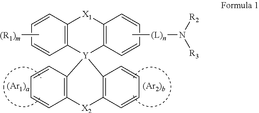


| TABLE 1 | ||||
| Device | ||||
| manufacturing | Hole transport | Voltage | Efficiency | Life |
| example | layer | (V) | (cd/A) | LT50 (h) |
| Example 1 | Example | 5.7 | 7.8 | 2100 |
| Compound A12 | ||||
| Example 2 | Example | 5.8 | 7.7 | 2200 |
| Compound A24 | ||||
| Example 3 | Example | 5.6 | 8.1 | 2000 |
| Compound A39 | ||||
| Example 4 | Example | 5.7 | 8.0 | 2050 |
| Compound A48 | ||||
| Example 5 | Example | 5.6 | 8.3 | 1950 |
| Compound A50 | ||||
| Example 6 | Example | 5.8 | 7.9 | 2000 |
| Compound A67 | ||||
| Example 7 | Example | 5.8 | 7.8 | 2100 |
| Compound | ||||
| A111 | ||||
| Example 8 | Example | 6.0 | 8.0 | 2000 |
| Compound | ||||
| A124 | ||||
| Example 9 | Example | 5.9 | 8.1 | 2050 |
| Compound | ||||
| A177 | ||||
| Comparative | Comparative | 6.2 | 6.2 | 1200 |
| Example 1 | Compound R1 | |||
| Comparative | Comparative | 6.0 | 6.2 | 1550 |
| Example 2 | Compound R2 | |||
| Comparative | Comparative | 6.0 | 6.4 | 1600 |
| Example 3 | Compound R3 | |||
| Comparative | Comparative | 6.0 | 6.7 | 1850 |
| Example 4 | Compound R4 | |||
| Comparative | Comparative | 6.1 | 6.5 | 1800 |
| Example 5 | Compound R5 | |||
| Comparative | Comparative | 6.1 | 6.6 | 1800 |
| Example 6 | Compound R6 | |||


| TABLE 2 | ||||
| Device | Life | |||
| manufacturing | Hole transport | Voltage | LT50 | |
| example | layer | (V) | Efficiency (Cd/A) | (h) |
| Example 10 | Example | 5.7 | 7.7 | 2150 |
| Compound B12 | ||||
| Example 11 | Example | 5.8 | 7.7 | 2200 |
| Compound B24 | ||||
| Example 12 | Example | 5.6 | 8.0 | 1950 |
| Compound B58 | ||||
| Example 13 | Example | 5.7 | 7.9 | 2000 |
| Compound B138 | ||||
| Example 14 | Example | 5.6 | 8.2 | 1900 |
| Compound B185 | ||||
| Example 15 | Example | 5.8 | 7.8 | 2100 |
| Compound B200 | ||||
| Example 16 | Example | 6.5 | 7.9 | 2100 |
| Compound B322 | ||||
| Example 17 | Example | 5.9 | 7.8 | 2050 |
| Compound B465 | ||||
| Comparative | Comparative | 6.0 | 6.7 | 1850 |
| Example 7 | Compound R7 | |||
| Comparative | Comparative | 6.0 | 6.8 | 1400 |
| Example 8 | Compound R8 | |||
| Comparative | Comparative | 6.0 | 6.7 | 1400 |
| Example 9 | Compound R9 | |||
| Comparative | Comparative | 6.0 | 6.6 | 1500 |
| Example 10 | Compound R10 | |||
Claims (19)


Applications Claiming Priority (2)
| Application Number | Priority Date | Filing Date | Title |
|---|---|---|---|
| KR10-2018-0060192 | 2018-05-28 | ||
| KR1020180060192A KR102607902B1 (en) | 2018-05-28 | 2018-05-28 | Organic electroluminescence device and monoamine compound for organic electroluminescence device |
Publications (2)
| Publication Number | Publication Date |
|---|---|
| US20190363263A1 US20190363263A1 (en) | 2019-11-28 |
| US11489125B2 true US11489125B2 (en) | 2022-11-01 |
Family
ID=66476423
Family Applications (1)
| Application Number | Title | Priority Date | Filing Date |
|---|---|---|---|
| US16/403,308 Active 2040-11-20 US11489125B2 (en) | 2018-05-28 | 2019-05-03 | Organic electroluminescence device and monoamine compound for organic electroluminescence device |
Country Status (5)
| Country | Link |
|---|---|
| US (1) | US11489125B2 (en) |
| EP (1) | EP3575304B1 (en) |
| JP (1) | JP7441008B2 (en) |
| KR (2) | KR102607902B1 (en) |
| CN (1) | CN110540545B (en) |
Families Citing this family (14)
| Publication number | Priority date | Publication date | Assignee | Title |
|---|---|---|---|---|
| CN110204567B (en) * | 2019-06-04 | 2020-12-04 | 武汉华星光电半导体显示技术有限公司 | Organic compound, application thereof and organic light-emitting diode electroluminescent device |
| CN112694464B (en) * | 2019-10-23 | 2024-04-16 | 乐金显示有限公司 | Organic compound and organic light-emitting display device using the same |
| US11072603B2 (en) * | 2019-11-19 | 2021-07-27 | Duk San Neolux Co., Ltd. | Compound for organic electronic element, organic electronic element using the same, and an electronic device thereof |
| CN114728948B (en) | 2019-11-19 | 2024-12-03 | 德山新勒克斯有限公司 | Compound for organic electronic element, organic electronic element using the compound, and electronic device thereof |
| US11925112B2 (en) | 2019-11-19 | 2024-03-05 | Duk San Neolux Co., Ltd. | Compound for organic electronic element, organic electronic element using the same, and an electronic device thereof |
| KR102853917B1 (en) * | 2020-01-20 | 2025-09-02 | 덕산네오룩스 주식회사 | Compound for organic electronic element, organic electronic element using the same, and an electronic device thereof |
| CN111620855B (en) * | 2020-06-12 | 2022-03-25 | 烟台九目化学股份有限公司 | Benzoxanthene compound-containing material and application thereof |
| KR102640225B1 (en) * | 2020-07-07 | 2024-02-23 | 주식회사 엘지화학 | Novel compound and organic light emitting device comprising the same |
| CN111675686A (en) * | 2020-07-09 | 2020-09-18 | 吉林奥来德光电材料股份有限公司 | An organic electroluminescent compound and its preparation method and application |
| KR102850721B1 (en) * | 2020-09-08 | 2025-08-25 | 주식회사 엘지화학 | Novel compound and organic light emitting device comprising the same |
| KR102880377B1 (en) | 2020-11-10 | 2025-11-05 | 삼성디스플레이 주식회사 | Light emitting diode and amine compound for the same |
| KR102807138B1 (en) | 2021-02-25 | 2025-05-12 | 삼성에스디아이 주식회사 | Compound for organic optoelectronic device, composition for organic optoelectronic device, organic optoelectronic device and display device |
| CN113582986B (en) * | 2021-07-21 | 2023-08-18 | 吉林奥来德光电材料股份有限公司 | Spiro compound and its preparation method, luminescence auxiliary material and organic electroluminescent device |
| KR20240001563A (en) * | 2022-06-27 | 2024-01-03 | 삼성에스디아이 주식회사 | Compound for organic optoelectronic device, organic optoelectronic device and display device |
Citations (22)
| Publication number | Priority date | Publication date | Assignee | Title |
|---|---|---|---|---|
| US6329082B1 (en) * | 1994-11-25 | 2001-12-11 | Hoechst Aktiengesellschaft | Hetero-spiro compounds and their use as electroluminescence materials |
| US6461748B1 (en) * | 2000-01-27 | 2002-10-08 | Canon Kabushiki Kaisha | Organic luminescence device with spiro compound having silicon spiro atom |
| US20040209115A1 (en) | 2003-04-21 | 2004-10-21 | Thompson Mark E. | Organic light emitting devices with wide gap host materials |
| US7014925B2 (en) * | 2003-04-29 | 2006-03-21 | Canon Kabushiki Kaisha | Heterogeneous spiro compounds in organic light emitting device elements |
| WO2010061315A1 (en) | 2008-11-26 | 2010-06-03 | Philips Intellectual Property & Standards Gmbh | Oled with novel hole-conducting material |
| WO2013139431A1 (en) | 2012-03-23 | 2013-09-26 | Merck Patent Gmbh | 9,9'-spirobixanthene derivatives for electroluminescent devices |
| KR20140025120A (en) | 2012-08-21 | 2014-03-04 | 제일모직주식회사 | Compound for organic optoelectronic device, organic light emitting diode including the same and display including the organic light emitting diode |
| KR20150106501A (en) | 2014-03-11 | 2015-09-22 | 삼성디스플레이 주식회사 | Compound and organic light emitting device comprising same |
| CN105154067A (en) | 2015-09-01 | 2015-12-16 | 华南理工大学 | Spiro-di-thioxanthene-based small-molecule luminescent material and preparation and application thereof |
| EP2980182A1 (en) | 2014-08-01 | 2016-02-03 | Samsung Electronics Co., Ltd. | Condensed cyclic compound and organic light-emitting device including the same |
| CN105778891A (en) | 2016-03-11 | 2016-07-20 | 中节能万润股份有限公司 | Organic optoelectronic material, preparation method thereof and organic light emitting diode containing organic material |
| CN105906640A (en) | 2016-05-12 | 2016-08-31 | 中节能万润股份有限公司 | Blue-ray doped material and preparation method and application thereof |
| KR20170082824A (en) | 2016-01-07 | 2017-07-17 | 주식회사 엘지화학 | Amine-based compound and organic light emitting device comprising the same |
| KR101781739B1 (en) | 2015-10-07 | 2017-09-25 | 주식회사 엘지화학 | New compound and organic light emitting device comprising the same |
| KR20170114369A (en) | 2016-04-04 | 2017-10-16 | 주식회사 두산 | Organic compound and organic electroluminescent device using the same |
| KR20170134163A (en) | 2016-05-27 | 2017-12-06 | 주식회사 엘지화학 | Organic light emitting device |
| KR20170138799A (en) | 2016-06-08 | 2017-12-18 | (주)씨엠디엘 | The novel organic electroluminescent compounds and organic electroluminescent device including the same |
| CN107586307A (en) | 2016-07-08 | 2018-01-16 | 上海和辉光电有限公司 | A kind of silicon fluorene derivative for blue light electroluminescence material |
| US20180309067A1 (en) * | 2017-04-21 | 2018-10-25 | Universal Display Corporation | Organic electroluminescent materials and devices |
| US20180315942A1 (en) * | 2017-04-28 | 2018-11-01 | Universal Display Corporation | Organic electroluminescent materials and devices |
| US20180337343A1 (en) * | 2017-05-18 | 2018-11-22 | Universal Display Corporation | Organic electroluminescent materials and devices |
| CN108976244A (en) | 2018-08-02 | 2018-12-11 | 华南理工大学 | The compound of the formula thioxanthene of spiral shell containing 9,9- and preparation and application |
Family Cites Families (1)
| Publication number | Priority date | Publication date | Assignee | Title |
|---|---|---|---|---|
| JP6580321B2 (en) | 2014-11-27 | 2019-09-25 | 三星ディスプレイ株式會社Samsung Display Co.,Ltd. | Monoamine derivative and organic electroluminescence device |
-
2018
- 2018-05-28 KR KR1020180060192A patent/KR102607902B1/en active Active
-
2019
- 2019-03-29 JP JP2019066881A patent/JP7441008B2/en active Active
- 2019-05-03 US US16/403,308 patent/US11489125B2/en active Active
- 2019-05-08 EP EP19173390.6A patent/EP3575304B1/en active Active
- 2019-05-22 CN CN201910428157.7A patent/CN110540545B/en active Active
-
2023
- 2023-11-24 KR KR1020230165802A patent/KR102758720B1/en active Active
Patent Citations (26)
| Publication number | Priority date | Publication date | Assignee | Title |
|---|---|---|---|---|
| US6329082B1 (en) * | 1994-11-25 | 2001-12-11 | Hoechst Aktiengesellschaft | Hetero-spiro compounds and their use as electroluminescence materials |
| US6461748B1 (en) * | 2000-01-27 | 2002-10-08 | Canon Kabushiki Kaisha | Organic luminescence device with spiro compound having silicon spiro atom |
| US20040209115A1 (en) | 2003-04-21 | 2004-10-21 | Thompson Mark E. | Organic light emitting devices with wide gap host materials |
| US7014925B2 (en) * | 2003-04-29 | 2006-03-21 | Canon Kabushiki Kaisha | Heterogeneous spiro compounds in organic light emitting device elements |
| WO2010061315A1 (en) | 2008-11-26 | 2010-06-03 | Philips Intellectual Property & Standards Gmbh | Oled with novel hole-conducting material |
| WO2013139431A1 (en) | 2012-03-23 | 2013-09-26 | Merck Patent Gmbh | 9,9'-spirobixanthene derivatives for electroluminescent devices |
| US20160329507A1 (en) * | 2012-03-23 | 2016-11-10 | Merck Patent Gmbh | 9,9'-spirobixanthene derivatives for electroluminescent devices |
| KR20140025120A (en) | 2012-08-21 | 2014-03-04 | 제일모직주식회사 | Compound for organic optoelectronic device, organic light emitting diode including the same and display including the organic light emitting diode |
| US20150162542A1 (en) | 2012-08-21 | 2015-06-11 | Samsung Sdi Co., Ltd. | Compound for organic optoelectronic device, organic light emitting diode including the same and display including the organic light emitting diode |
| KR20150106501A (en) | 2014-03-11 | 2015-09-22 | 삼성디스플레이 주식회사 | Compound and organic light emitting device comprising same |
| EP2980182A1 (en) | 2014-08-01 | 2016-02-03 | Samsung Electronics Co., Ltd. | Condensed cyclic compound and organic light-emitting device including the same |
| US20160035986A1 (en) * | 2014-08-01 | 2016-02-04 | Samsung Electronics Co., Ltd. | Condensed cyclic compound and organic light-emitting device including the same |
| CN105154067A (en) | 2015-09-01 | 2015-12-16 | 华南理工大学 | Spiro-di-thioxanthene-based small-molecule luminescent material and preparation and application thereof |
| KR101781739B1 (en) | 2015-10-07 | 2017-09-25 | 주식회사 엘지화학 | New compound and organic light emitting device comprising the same |
| US20180287068A1 (en) | 2015-10-07 | 2018-10-04 | Lg Chem, Ltd. | Novel compound and organic light emitting diode comprising same |
| KR20170082824A (en) | 2016-01-07 | 2017-07-17 | 주식회사 엘지화학 | Amine-based compound and organic light emitting device comprising the same |
| CN105778891A (en) | 2016-03-11 | 2016-07-20 | 中节能万润股份有限公司 | Organic optoelectronic material, preparation method thereof and organic light emitting diode containing organic material |
| KR20170114369A (en) | 2016-04-04 | 2017-10-16 | 주식회사 두산 | Organic compound and organic electroluminescent device using the same |
| CN105906640A (en) | 2016-05-12 | 2016-08-31 | 中节能万润股份有限公司 | Blue-ray doped material and preparation method and application thereof |
| KR20170134163A (en) | 2016-05-27 | 2017-12-06 | 주식회사 엘지화학 | Organic light emitting device |
| KR20170138799A (en) | 2016-06-08 | 2017-12-18 | (주)씨엠디엘 | The novel organic electroluminescent compounds and organic electroluminescent device including the same |
| CN107586307A (en) | 2016-07-08 | 2018-01-16 | 上海和辉光电有限公司 | A kind of silicon fluorene derivative for blue light electroluminescence material |
| US20180309067A1 (en) * | 2017-04-21 | 2018-10-25 | Universal Display Corporation | Organic electroluminescent materials and devices |
| US20180315942A1 (en) * | 2017-04-28 | 2018-11-01 | Universal Display Corporation | Organic electroluminescent materials and devices |
| US20180337343A1 (en) * | 2017-05-18 | 2018-11-22 | Universal Display Corporation | Organic electroluminescent materials and devices |
| CN108976244A (en) | 2018-08-02 | 2018-12-11 | 华南理工大学 | The compound of the formula thioxanthene of spiral shell containing 9,9- and preparation and application |
Non-Patent Citations (2)
| Title |
|---|
| Machine translation of CN-105154067, translation generated Apr. 2021, 31 pages. (Year: 2021). * |
| Partial European Search Report for corresponding European Patent Application No. 19173390.6, dated Jul. 16, 2019, 11 pages. |
Also Published As
| Publication number | Publication date |
|---|---|
| JP7441008B2 (en) | 2024-02-29 |
| KR102758720B1 (en) | 2025-01-24 |
| EP3575304B1 (en) | 2022-03-09 |
| US20190363263A1 (en) | 2019-11-28 |
| KR20230169878A (en) | 2023-12-18 |
| JP2019206512A (en) | 2019-12-05 |
| KR20190135579A (en) | 2019-12-09 |
| CN110540545A (en) | 2019-12-06 |
| KR102607902B1 (en) | 2023-11-30 |
| CN110540545B (en) | 2024-04-09 |
| EP3575304A1 (en) | 2019-12-04 |
Similar Documents
| Publication | Publication Date | Title |
|---|---|---|
| US11489125B2 (en) | Organic electroluminescence device and monoamine compound for organic electroluminescence device | |
| US12497389B2 (en) | Organic electroluminescence device and heterocyclic compound for organic electroluminescence device | |
| US12391668B2 (en) | Organic electroluminescence device and polycyclic compound for organic electroluminescence device | |
| US11653561B2 (en) | Organic electroluminescence device and fused polycyclic compound for organic electroluminescence device | |
| US20190312210A1 (en) | Organic electroluminescence device and polycyclic compound for organic electroluminescence device | |
| US11393985B2 (en) | Organic electroluminescence device and polycyclic compound for organic electroluminescence device | |
| US12144251B2 (en) | Organic electroluminescence device and condensed cyclic compound for organic electroluminescence device | |
| US11825744B2 (en) | Organic electroluminescence device and condensed cyclic compound for organic electroluminescence device | |
| US11515486B2 (en) | Organic electroluminescence device and polycyclic compound for organic electroluminescence device | |
| US12096682B2 (en) | Organic electroluminescence device and monoamine compound for organic electroluminescence device | |
| US20210175431A1 (en) | Organic electroluminescence device and condensed polycyclic compound for organic electroluminescence device | |
| US12150378B2 (en) | Luminescence device and polycyclic compound for luminescence device | |
| US20200283426A1 (en) | Organic electroluminescence device and polycyclic compound for organic electroluminescence device | |
| US20210399227A1 (en) | Organic electroluminescence device and fused polycyclic compound for organic electroluminescence device | |
| US11737355B2 (en) | Organic electroluminescence device and amine compound for organic electroluminescence device | |
| US10777753B2 (en) | Heterocyclic compound and organic electroluminescence device including the same | |
| US12439820B2 (en) | Organic electroluminescence device and amine compound for organic electroluminescence device | |
| US11450821B2 (en) | Organic electroluminescence device and polycyclic compound for organic electroluminescence device | |
| US11264573B2 (en) | Organic electroluminescence device and amine compound for organic electroluminescence device | |
| US12022733B2 (en) | Organic electroluminescence device and monoamine compound for organic electroluminescence device | |
| US11805695B2 (en) | Organic electroluminescence device and polycyclic compound for organic electroluminescence device | |
| US12528820B2 (en) | Luminescence device and polycyclic compound for luminescence device | |
| US11770973B2 (en) | Organic electroluminescence device and amine compound for organic electroluminescence device |
Legal Events
| Date | Code | Title | Description |
|---|---|---|---|
| FEPP | Fee payment procedure |
Free format text: ENTITY STATUS SET TO UNDISCOUNTED (ORIGINAL EVENT CODE: BIG.); ENTITY STATUS OF PATENT OWNER: LARGE ENTITY |
|
| AS | Assignment |
Owner name: SAMSUNG DISPLAY CO., LTD., KOREA, REPUBLIC OF Free format text: ASSIGNMENT OF ASSIGNORS INTEREST;ASSIGNOR:UNO, TAKUYA;REEL/FRAME:049239/0885 Effective date: 20190121 |
|
| STPP | Information on status: patent application and granting procedure in general |
Free format text: NON FINAL ACTION MAILED |
|
| STPP | Information on status: patent application and granting procedure in general |
Free format text: RESPONSE TO NON-FINAL OFFICE ACTION ENTERED AND FORWARDED TO EXAMINER |
|
| STPP | Information on status: patent application and granting procedure in general |
Free format text: NOTICE OF ALLOWANCE MAILED -- APPLICATION RECEIVED IN OFFICE OF PUBLICATIONS |
|
| STPP | Information on status: patent application and granting procedure in general |
Free format text: AWAITING TC RESP., ISSUE FEE NOT PAID |
|
| STPP | Information on status: patent application and granting procedure in general |
Free format text: NOTICE OF ALLOWANCE MAILED -- APPLICATION RECEIVED IN OFFICE OF PUBLICATIONS |
|
| STPP | Information on status: patent application and granting procedure in general |
Free format text: PUBLICATIONS -- ISSUE FEE PAYMENT VERIFIED |
|
| STCF | Information on status: patent grant |
Free format text: PATENTED CASE |