US11444207B2 - Lithium drifted thin film transistors for neuromorphic computing - Google Patents
Lithium drifted thin film transistors for neuromorphic computing Download PDFInfo
- Publication number
- US11444207B2 US11444207B2 US16/217,651 US201816217651A US11444207B2 US 11444207 B2 US11444207 B2 US 11444207B2 US 201816217651 A US201816217651 A US 201816217651A US 11444207 B2 US11444207 B2 US 11444207B2
- Authority
- US
- United States
- Prior art keywords
- lithium
- gate
- source
- semiconductor device
- effect transistor
- Prior art date
- Legal status (The legal status is an assumption and is not a legal conclusion. Google has not performed a legal analysis and makes no representation as to the accuracy of the status listed.)
- Active, expires
Links
- WHXSMMKQMYFTQS-UHFFFAOYSA-N Lithium Chemical compound [Li] WHXSMMKQMYFTQS-UHFFFAOYSA-N 0.000 title claims abstract description 92
- 229910052744 lithium Inorganic materials 0.000 title claims abstract description 90
- 239000010409 thin film Substances 0.000 title description 2
- 239000004065 semiconductor Substances 0.000 claims abstract description 58
- 238000001465 metallisation Methods 0.000 claims abstract description 43
- 230000005669 field effect Effects 0.000 claims abstract description 27
- 229910021420 polycrystalline silicon Inorganic materials 0.000 claims description 29
- 239000002019 doping agent Substances 0.000 claims description 15
- 229910052732 germanium Inorganic materials 0.000 claims description 10
- GNPVGFCGXDBREM-UHFFFAOYSA-N germanium atom Chemical compound [Ge] GNPVGFCGXDBREM-UHFFFAOYSA-N 0.000 claims description 10
- 238000012545 processing Methods 0.000 claims description 6
- 229910021417 amorphous silicon Inorganic materials 0.000 claims description 4
- 229910052751 metal Inorganic materials 0.000 description 77
- 239000002184 metal Substances 0.000 description 77
- 239000000463 material Substances 0.000 description 47
- 238000000034 method Methods 0.000 description 27
- 229920005591 polysilicon Polymers 0.000 description 26
- 230000008569 process Effects 0.000 description 19
- 238000000151 deposition Methods 0.000 description 18
- 125000006850 spacer group Chemical group 0.000 description 16
- 230000008021 deposition Effects 0.000 description 15
- 239000000758 substrate Substances 0.000 description 15
- 238000002513 implantation Methods 0.000 description 13
- 230000008859 change Effects 0.000 description 9
- 238000011065 in-situ storage Methods 0.000 description 9
- 229910000577 Silicon-germanium Inorganic materials 0.000 description 8
- 229910003811 SiGeC Inorganic materials 0.000 description 7
- NRTOMJZYCJJWKI-UHFFFAOYSA-N Titanium nitride Chemical compound [Ti]#N NRTOMJZYCJJWKI-UHFFFAOYSA-N 0.000 description 7
- 229910003465 moissanite Inorganic materials 0.000 description 7
- 229910010271 silicon carbide Inorganic materials 0.000 description 7
- 229910052721 tungsten Inorganic materials 0.000 description 7
- ZOXJGFHDIHLPTG-UHFFFAOYSA-N Boron Chemical compound [B] ZOXJGFHDIHLPTG-UHFFFAOYSA-N 0.000 description 6
- OAICVXFJPJFONN-UHFFFAOYSA-N Phosphorus Chemical compound [P] OAICVXFJPJFONN-UHFFFAOYSA-N 0.000 description 6
- 229910045601 alloy Inorganic materials 0.000 description 6
- 239000000956 alloy Substances 0.000 description 6
- 229910052785 arsenic Inorganic materials 0.000 description 6
- RQNWIZPPADIBDY-UHFFFAOYSA-N arsenic atom Chemical compound [As] RQNWIZPPADIBDY-UHFFFAOYSA-N 0.000 description 6
- 229910052796 boron Inorganic materials 0.000 description 6
- 229910052698 phosphorus Inorganic materials 0.000 description 6
- 239000011574 phosphorus Substances 0.000 description 6
- VYPSYNLAJGMNEJ-UHFFFAOYSA-N Silicium dioxide Chemical compound O=[Si]=O VYPSYNLAJGMNEJ-UHFFFAOYSA-N 0.000 description 5
- XUIMIQQOPSSXEZ-UHFFFAOYSA-N Silicon Chemical compound [Si] XUIMIQQOPSSXEZ-UHFFFAOYSA-N 0.000 description 5
- 238000003491 array Methods 0.000 description 5
- 239000007943 implant Substances 0.000 description 5
- 229910052710 silicon Inorganic materials 0.000 description 5
- 239000010703 silicon Substances 0.000 description 5
- 229910052814 silicon oxide Inorganic materials 0.000 description 5
- 229910052581 Si3N4 Inorganic materials 0.000 description 4
- 238000005229 chemical vapour deposition Methods 0.000 description 4
- 230000010354 integration Effects 0.000 description 4
- HQVNEWCFYHHQES-UHFFFAOYSA-N silicon nitride Chemical compound N12[Si]34N5[Si]62N3[Si]51N64 HQVNEWCFYHHQES-UHFFFAOYSA-N 0.000 description 4
- HBBGRARXTFLTSG-UHFFFAOYSA-N Lithium ion Chemical compound [Li+] HBBGRARXTFLTSG-UHFFFAOYSA-N 0.000 description 3
- 239000003990 capacitor Substances 0.000 description 3
- 239000007789 gas Substances 0.000 description 3
- 229910001416 lithium ion Inorganic materials 0.000 description 3
- 238000004519 manufacturing process Methods 0.000 description 3
- 238000000623 plasma-assisted chemical vapour deposition Methods 0.000 description 3
- 230000004044 response Effects 0.000 description 3
- -1 tetrasilane Chemical compound 0.000 description 3
- OKTJSMMVPCPJKN-UHFFFAOYSA-N Carbon Chemical compound [C] OKTJSMMVPCPJKN-UHFFFAOYSA-N 0.000 description 2
- 238000013528 artificial neural network Methods 0.000 description 2
- 238000000231 atomic layer deposition Methods 0.000 description 2
- 229910052799 carbon Inorganic materials 0.000 description 2
- 238000004891 communication Methods 0.000 description 2
- 239000013078 crystal Substances 0.000 description 2
- 239000002178 crystalline material Substances 0.000 description 2
- 230000007547 defect Effects 0.000 description 2
- 238000005137 deposition process Methods 0.000 description 2
- 230000005684 electric field Effects 0.000 description 2
- 230000003116 impacting effect Effects 0.000 description 2
- 239000011159 matrix material Substances 0.000 description 2
- NJPPVKZQTLUDBO-UHFFFAOYSA-N novaluron Chemical compound C1=C(Cl)C(OC(F)(F)C(OC(F)(F)F)F)=CC=C1NC(=O)NC(=O)C1=C(F)C=CC=C1F NJPPVKZQTLUDBO-UHFFFAOYSA-N 0.000 description 2
- 238000005240 physical vapour deposition Methods 0.000 description 2
- 238000004549 pulsed laser deposition Methods 0.000 description 2
- OFIYHXOOOISSDN-UHFFFAOYSA-N tellanylidenegallium Chemical compound [Te]=[Ga] OFIYHXOOOISSDN-UHFFFAOYSA-N 0.000 description 2
- 239000010936 titanium Substances 0.000 description 2
- 229910052582 BN Inorganic materials 0.000 description 1
- PZNSFCLAULLKQX-UHFFFAOYSA-N Boron nitride Chemical compound N#B PZNSFCLAULLKQX-UHFFFAOYSA-N 0.000 description 1
- RYGMFSIKBFXOCR-UHFFFAOYSA-N Copper Chemical compound [Cu] RYGMFSIKBFXOCR-UHFFFAOYSA-N 0.000 description 1
- KJTLSVCANCCWHF-UHFFFAOYSA-N Ruthenium Chemical compound [Ru] KJTLSVCANCCWHF-UHFFFAOYSA-N 0.000 description 1
- BLRPTPMANUNPDV-UHFFFAOYSA-N Silane Chemical compound [SiH4] BLRPTPMANUNPDV-UHFFFAOYSA-N 0.000 description 1
- RTAQQCXQSZGOHL-UHFFFAOYSA-N Titanium Chemical compound [Ti] RTAQQCXQSZGOHL-UHFFFAOYSA-N 0.000 description 1
- CFOAUMXQOCBWNJ-UHFFFAOYSA-N [B].[Si] Chemical compound [B].[Si] CFOAUMXQOCBWNJ-UHFFFAOYSA-N 0.000 description 1
- ZILJFRYKLPPLTO-UHFFFAOYSA-N [C].[B].[Si] Chemical compound [C].[B].[Si] ZILJFRYKLPPLTO-UHFFFAOYSA-N 0.000 description 1
- HMDDXIMCDZRSNE-UHFFFAOYSA-N [C].[Si] Chemical compound [C].[Si] HMDDXIMCDZRSNE-UHFFFAOYSA-N 0.000 description 1
- ZVLDJSZFKQJMKD-UHFFFAOYSA-N [Li].[Si] Chemical compound [Li].[Si] ZVLDJSZFKQJMKD-UHFFFAOYSA-N 0.000 description 1
- 230000004888 barrier function Effects 0.000 description 1
- 238000005234 chemical deposition Methods 0.000 description 1
- 239000010941 cobalt Substances 0.000 description 1
- 229910017052 cobalt Inorganic materials 0.000 description 1
- GUTLYIVDDKVIGB-UHFFFAOYSA-N cobalt atom Chemical compound [Co] GUTLYIVDDKVIGB-UHFFFAOYSA-N 0.000 description 1
- 229910052802 copper Inorganic materials 0.000 description 1
- 239000010949 copper Substances 0.000 description 1
- 238000005336 cracking Methods 0.000 description 1
- 238000013461 design Methods 0.000 description 1
- OXTURSYJKMYFLT-UHFFFAOYSA-N dichlorogermane Chemical compound Cl[GeH2]Cl OXTURSYJKMYFLT-UHFFFAOYSA-N 0.000 description 1
- MROCJMGDEKINLD-UHFFFAOYSA-N dichlorosilane Chemical compound Cl[SiH2]Cl MROCJMGDEKINLD-UHFFFAOYSA-N 0.000 description 1
- 238000009792 diffusion process Methods 0.000 description 1
- VXGHASBVNMHGDI-UHFFFAOYSA-N digermane Chemical compound [Ge][Ge] VXGHASBVNMHGDI-UHFFFAOYSA-N 0.000 description 1
- PZPGRFITIJYNEJ-UHFFFAOYSA-N disilane Chemical compound [SiH3][SiH3] PZPGRFITIJYNEJ-UHFFFAOYSA-N 0.000 description 1
- 238000005516 engineering process Methods 0.000 description 1
- 239000010408 film Substances 0.000 description 1
- 229910000078 germane Inorganic materials 0.000 description 1
- 239000011810 insulating material Substances 0.000 description 1
- 239000007788 liquid Substances 0.000 description 1
- 238000010801 machine learning Methods 0.000 description 1
- 230000001404 mediated effect Effects 0.000 description 1
- 230000003278 mimic effect Effects 0.000 description 1
- 238000012986 modification Methods 0.000 description 1
- 230000004048 modification Effects 0.000 description 1
- 210000000653 nervous system Anatomy 0.000 description 1
- 238000000059 patterning Methods 0.000 description 1
- 239000012782 phase change material Substances 0.000 description 1
- 238000002135 phase contrast microscopy Methods 0.000 description 1
- 238000007747 plating Methods 0.000 description 1
- 239000000376 reactant Substances 0.000 description 1
- 229910052707 ruthenium Inorganic materials 0.000 description 1
- 229910000077 silane Inorganic materials 0.000 description 1
- FDNAPBUWERUEDA-UHFFFAOYSA-N silicon tetrachloride Chemical compound Cl[Si](Cl)(Cl)Cl FDNAPBUWERUEDA-UHFFFAOYSA-N 0.000 description 1
- 238000004544 sputter deposition Methods 0.000 description 1
- 238000003860 storage Methods 0.000 description 1
- 239000000126 substance Substances 0.000 description 1
- IEXRMSFAVATTJX-UHFFFAOYSA-N tetrachlorogermane Chemical compound Cl[Ge](Cl)(Cl)Cl IEXRMSFAVATTJX-UHFFFAOYSA-N 0.000 description 1
- 238000000427 thin-film deposition Methods 0.000 description 1
- 229910052719 titanium Inorganic materials 0.000 description 1
- LXEXBJXDGVGRAR-UHFFFAOYSA-N trichloro(trichlorosilyl)silane Chemical compound Cl[Si](Cl)(Cl)[Si](Cl)(Cl)Cl LXEXBJXDGVGRAR-UHFFFAOYSA-N 0.000 description 1
- MUDDKLJPADVVKF-UHFFFAOYSA-N trichlorogermane Chemical compound Cl[GeH](Cl)Cl MUDDKLJPADVVKF-UHFFFAOYSA-N 0.000 description 1
- ZDHXKXAHOVTTAH-UHFFFAOYSA-N trichlorosilane Chemical compound Cl[SiH](Cl)Cl ZDHXKXAHOVTTAH-UHFFFAOYSA-N 0.000 description 1
- 239000005052 trichlorosilane Substances 0.000 description 1
- VEDJZFSRVVQBIL-UHFFFAOYSA-N trisilane Chemical compound [SiH3][SiH2][SiH3] VEDJZFSRVVQBIL-UHFFFAOYSA-N 0.000 description 1
- WFKWXMTUELFFGS-UHFFFAOYSA-N tungsten Chemical compound [W] WFKWXMTUELFFGS-UHFFFAOYSA-N 0.000 description 1
- 239000010937 tungsten Substances 0.000 description 1
Images


Classifications
-
- H—ELECTRICITY
- H01—ELECTRIC ELEMENTS
- H01L—SEMICONDUCTOR DEVICES NOT COVERED BY CLASS H10
- H01L29/00—Semiconductor devices adapted for rectifying, amplifying, oscillating or switching, or capacitors or resistors with at least one potential-jump barrier or surface barrier, e.g. PN junction depletion layer or carrier concentration layer; Details of semiconductor bodies or of electrodes thereof ; Multistep manufacturing processes therefor
- H01L29/02—Semiconductor bodies ; Multistep manufacturing processes therefor
- H01L29/06—Semiconductor bodies ; Multistep manufacturing processes therefor characterised by their shape; characterised by the shapes, relative sizes, or dispositions of the semiconductor regions ; characterised by the concentration or distribution of impurities within semiconductor regions
- H01L29/10—Semiconductor bodies ; Multistep manufacturing processes therefor characterised by their shape; characterised by the shapes, relative sizes, or dispositions of the semiconductor regions ; characterised by the concentration or distribution of impurities within semiconductor regions with semiconductor regions connected to an electrode not carrying current to be rectified, amplified or switched and such electrode being part of a semiconductor device which comprises three or more electrodes
- H01L29/1025—Channel region of field-effect devices
- H01L29/1029—Channel region of field-effect devices of field-effect transistors
- H01L29/1033—Channel region of field-effect devices of field-effect transistors with insulated gate, e.g. characterised by the length, the width, the geometric contour or the doping structure
-
- H—ELECTRICITY
- H01—ELECTRIC ELEMENTS
- H01L—SEMICONDUCTOR DEVICES NOT COVERED BY CLASS H10
- H01L29/00—Semiconductor devices adapted for rectifying, amplifying, oscillating or switching, or capacitors or resistors with at least one potential-jump barrier or surface barrier, e.g. PN junction depletion layer or carrier concentration layer; Details of semiconductor bodies or of electrodes thereof ; Multistep manufacturing processes therefor
- H01L29/66—Types of semiconductor device ; Multistep manufacturing processes therefor
- H01L29/68—Types of semiconductor device ; Multistep manufacturing processes therefor controllable by only the electric current supplied, or only the electric potential applied, to an electrode which does not carry the current to be rectified, amplified or switched
- H01L29/76—Unipolar devices, e.g. field effect transistors
- H01L29/772—Field effect transistors
- H01L29/78—Field effect transistors with field effect produced by an insulated gate
- H01L29/786—Thin film transistors, i.e. transistors with a channel being at least partly a thin film
- H01L29/78696—Thin film transistors, i.e. transistors with a channel being at least partly a thin film characterised by the structure of the channel, e.g. multichannel, transverse or longitudinal shape, length or width, doping structure, or the overlap or alignment between the channel and the gate, the source or the drain, or the contacting structure of the channel
-
- H—ELECTRICITY
- H01—ELECTRIC ELEMENTS
- H01L—SEMICONDUCTOR DEVICES NOT COVERED BY CLASS H10
- H01L21/00—Processes or apparatus adapted for the manufacture or treatment of semiconductor or solid state devices or of parts thereof
- H01L21/02—Manufacture or treatment of semiconductor devices or of parts thereof
- H01L21/04—Manufacture or treatment of semiconductor devices or of parts thereof the devices having at least one potential-jump barrier or surface barrier, e.g. PN junction, depletion layer or carrier concentration layer
- H01L21/18—Manufacture or treatment of semiconductor devices or of parts thereof the devices having at least one potential-jump barrier or surface barrier, e.g. PN junction, depletion layer or carrier concentration layer the devices having semiconductor bodies comprising elements of Group IV of the Periodic System or AIIIBV compounds with or without impurities, e.g. doping materials
- H01L21/26—Bombardment with radiation
- H01L21/263—Bombardment with radiation with high-energy radiation
- H01L21/265—Bombardment with radiation with high-energy radiation producing ion implantation
- H01L21/26506—Bombardment with radiation with high-energy radiation producing ion implantation in group IV semiconductors
-
- H—ELECTRICITY
- H01—ELECTRIC ELEMENTS
- H01L—SEMICONDUCTOR DEVICES NOT COVERED BY CLASS H10
- H01L21/00—Processes or apparatus adapted for the manufacture or treatment of semiconductor or solid state devices or of parts thereof
- H01L21/02—Manufacture or treatment of semiconductor devices or of parts thereof
- H01L21/04—Manufacture or treatment of semiconductor devices or of parts thereof the devices having at least one potential-jump barrier or surface barrier, e.g. PN junction, depletion layer or carrier concentration layer
- H01L21/18—Manufacture or treatment of semiconductor devices or of parts thereof the devices having at least one potential-jump barrier or surface barrier, e.g. PN junction, depletion layer or carrier concentration layer the devices having semiconductor bodies comprising elements of Group IV of the Periodic System or AIIIBV compounds with or without impurities, e.g. doping materials
- H01L21/28—Manufacture of electrodes on semiconductor bodies using processes or apparatus not provided for in groups H01L21/20 - H01L21/268
- H01L21/28008—Making conductor-insulator-semiconductor electrodes
- H01L21/28017—Making conductor-insulator-semiconductor electrodes the insulator being formed after the semiconductor body, the semiconductor being silicon
- H01L21/28158—Making the insulator
- H01L21/2822—Making the insulator with substrate doping, e.g. N, Ge, C implantation, before formation of the insulator
-
- H—ELECTRICITY
- H01—ELECTRIC ELEMENTS
- H01L—SEMICONDUCTOR DEVICES NOT COVERED BY CLASS H10
- H01L21/00—Processes or apparatus adapted for the manufacture or treatment of semiconductor or solid state devices or of parts thereof
- H01L21/02—Manufacture or treatment of semiconductor devices or of parts thereof
- H01L21/04—Manufacture or treatment of semiconductor devices or of parts thereof the devices having at least one potential-jump barrier or surface barrier, e.g. PN junction, depletion layer or carrier concentration layer
- H01L21/18—Manufacture or treatment of semiconductor devices or of parts thereof the devices having at least one potential-jump barrier or surface barrier, e.g. PN junction, depletion layer or carrier concentration layer the devices having semiconductor bodies comprising elements of Group IV of the Periodic System or AIIIBV compounds with or without impurities, e.g. doping materials
- H01L21/28—Manufacture of electrodes on semiconductor bodies using processes or apparatus not provided for in groups H01L21/20 - H01L21/268
- H01L21/28008—Making conductor-insulator-semiconductor electrodes
- H01L21/28255—Making conductor-insulator-semiconductor electrodes the insulator being formed after the semiconductor body, the semiconductor belonging to Group IV and not being elemental silicon, e.g. Ge, SiGe, SiGeC
-
- H—ELECTRICITY
- H01—ELECTRIC ELEMENTS
- H01L—SEMICONDUCTOR DEVICES NOT COVERED BY CLASS H10
- H01L29/00—Semiconductor devices adapted for rectifying, amplifying, oscillating or switching, or capacitors or resistors with at least one potential-jump barrier or surface barrier, e.g. PN junction depletion layer or carrier concentration layer; Details of semiconductor bodies or of electrodes thereof ; Multistep manufacturing processes therefor
- H01L29/02—Semiconductor bodies ; Multistep manufacturing processes therefor
- H01L29/06—Semiconductor bodies ; Multistep manufacturing processes therefor characterised by their shape; characterised by the shapes, relative sizes, or dispositions of the semiconductor regions ; characterised by the concentration or distribution of impurities within semiconductor regions
- H01L29/08—Semiconductor bodies ; Multistep manufacturing processes therefor characterised by their shape; characterised by the shapes, relative sizes, or dispositions of the semiconductor regions ; characterised by the concentration or distribution of impurities within semiconductor regions with semiconductor regions connected to an electrode carrying current to be rectified, amplified or switched and such electrode being part of a semiconductor device which comprises three or more electrodes
- H01L29/0843—Source or drain regions of field-effect devices
- H01L29/0847—Source or drain regions of field-effect devices of field-effect transistors with insulated gate
-
- H—ELECTRICITY
- H01—ELECTRIC ELEMENTS
- H01L—SEMICONDUCTOR DEVICES NOT COVERED BY CLASS H10
- H01L29/00—Semiconductor devices adapted for rectifying, amplifying, oscillating or switching, or capacitors or resistors with at least one potential-jump barrier or surface barrier, e.g. PN junction depletion layer or carrier concentration layer; Details of semiconductor bodies or of electrodes thereof ; Multistep manufacturing processes therefor
- H01L29/40—Electrodes ; Multistep manufacturing processes therefor
- H01L29/43—Electrodes ; Multistep manufacturing processes therefor characterised by the materials of which they are formed
- H01L29/49—Metal-insulator-semiconductor electrodes, e.g. gates of MOSFET
- H01L29/4908—Metal-insulator-semiconductor electrodes, e.g. gates of MOSFET for thin film semiconductor, e.g. gate of TFT
-
- H—ELECTRICITY
- H01—ELECTRIC ELEMENTS
- H01L—SEMICONDUCTOR DEVICES NOT COVERED BY CLASS H10
- H01L29/00—Semiconductor devices adapted for rectifying, amplifying, oscillating or switching, or capacitors or resistors with at least one potential-jump barrier or surface barrier, e.g. PN junction depletion layer or carrier concentration layer; Details of semiconductor bodies or of electrodes thereof ; Multistep manufacturing processes therefor
- H01L29/66—Types of semiconductor device ; Multistep manufacturing processes therefor
- H01L29/66007—Multistep manufacturing processes
- H01L29/66075—Multistep manufacturing processes of devices having semiconductor bodies comprising group 14 or group 13/15 materials
- H01L29/66227—Multistep manufacturing processes of devices having semiconductor bodies comprising group 14 or group 13/15 materials the devices being controllable only by the electric current supplied or the electric potential applied, to an electrode which does not carry the current to be rectified, amplified or switched, e.g. three-terminal devices
- H01L29/66409—Unipolar field-effect transistors
- H01L29/66477—Unipolar field-effect transistors with an insulated gate, i.e. MISFET
- H01L29/66742—Thin film unipolar transistors
- H01L29/6675—Amorphous silicon or polysilicon transistors
-
- H—ELECTRICITY
- H01—ELECTRIC ELEMENTS
- H01L—SEMICONDUCTOR DEVICES NOT COVERED BY CLASS H10
- H01L29/00—Semiconductor devices adapted for rectifying, amplifying, oscillating or switching, or capacitors or resistors with at least one potential-jump barrier or surface barrier, e.g. PN junction depletion layer or carrier concentration layer; Details of semiconductor bodies or of electrodes thereof ; Multistep manufacturing processes therefor
- H01L29/66—Types of semiconductor device ; Multistep manufacturing processes therefor
- H01L29/68—Types of semiconductor device ; Multistep manufacturing processes therefor controllable by only the electric current supplied, or only the electric potential applied, to an electrode which does not carry the current to be rectified, amplified or switched
- H01L29/76—Unipolar devices, e.g. field effect transistors
- H01L29/772—Field effect transistors
- H01L29/78—Field effect transistors with field effect produced by an insulated gate
- H01L29/786—Thin film transistors, i.e. transistors with a channel being at least partly a thin film
- H01L29/78651—Silicon transistors
- H01L29/7866—Non-monocrystalline silicon transistors
- H01L29/78672—Polycrystalline or microcrystalline silicon transistor
-
- G—PHYSICS
- G06—COMPUTING; CALCULATING OR COUNTING
- G06N—COMPUTING ARRANGEMENTS BASED ON SPECIFIC COMPUTATIONAL MODELS
- G06N3/00—Computing arrangements based on biological models
- G06N3/02—Neural networks
- G06N3/06—Physical realisation, i.e. hardware implementation of neural networks, neurons or parts of neurons
- G06N3/063—Physical realisation, i.e. hardware implementation of neural networks, neurons or parts of neurons using electronic means
- G06N3/065—Analogue means
Definitions
- the field generally relates to semiconductor devices and methods of manufacturing same and, in particular, to integrating lithium-implanted FETs in the back-end-of-line (BEOL) to be used in place of the resistive elements for resistive processing units (RPUs).
- BEOL back-end-of-line
- RPUs resistive processing units
- neuromorphic computing utilizes very-large-scale integration (VLSI) systems containing analog circuits to mimic neuro-biological architectures present in the nervous system.
- VLSI very-large-scale integration
- arrays of trainable resistive devices referred to as resistive processing units (RPUs)
- RPUs resistive processing units
- ANNs artificial neural networks
- RPU architecture includes a plurality of non-volatile resistive elements, such as phase change devices, each in series with a field-effect transistor (FET) connected in a diode configuration, that change their states after application of a certain voltage.
- non-volatile resistive elements such as phase change devices
- FET field-effect transistor
- conventional RPU devices are implemented with resistive random access memory (RRAM), phase change memory (PCM), programmable metallization cell (PMC) memory, non-linear memristive systems, or any other two-terminal device that has non-linear resistive switching characteristics.
- RRAM resistive random access memory
- PCM phase change memory
- PMC programmable metallization cell
- RPUs which are resistive elements each having an updateable resistive weight.
- Input voltages are respectively applied to the row wires, and each column wire sums currents generated by each RPU along a particular column wire.
- forward matrix multiplication of the array is computed by multiplying values stored in the RPUs by the row wire voltage inputs.
- backward matrix multiplication of the array is computed by voltages are applied at respective voltages column wires instead of the row wires, reading current from the row wires.
- a semiconductor device includes a field-effect transistor, a first back-end-of-line (BEOL) metallization level and a second BEOL metallization level disposed above the first BEOL metallization level.
- a portion of the field-effect transistor includes lithium therein, and the field-effect transistor is integrated between the first and second BEOL metallization levels.
- a method for manufacturing a semiconductor device includes forming a field-effect transistor, and implanting lithium into a portion of the field-effect transistor.
- a first back-end-of-line (BEOL) metallization level, and a second BEOL metallization level above the first BEOL metallization level are formed.
- the field-effect transistor is integrated between the first and second BEOL metallization levels.
- a semiconductor device includes an array of resistive processing unit (RPU) devices.
- Each RPU device in the array includes a field-effect transistor integrated between a first back-end-of-line (BEOL) metallization level and a second BEOL metallization level above the first BEOL metallization level.
- a portion of each field-effect transistor includes lithium therein, and a gate of each field-effect transistor is electrically connected to a contact of the second BEOL metallization level.
- FIG. 1 is a cross-sectional view illustrating a polysilicon gate thin-film transistor (TFT) on a back gate and including a channel region implanted with lithium, according to an exemplary embodiment of the present invention.
- TFT polysilicon gate thin-film transistor
- FIG. 2 is a cross-sectional view illustrating a polysilicon gate TFT on a back gate and including source and drain regions implanted with lithium, according to an exemplary embodiment of the present invention.
- FIG. 3 is a cross-sectional view illustrating a polysilicon gate TFT on a back gate and including a drain region implanted with lithium, according to an exemplary embodiment of the present invention.
- FIG. 4A is a graph illustrating threshold voltage change due to lithium drift, according to an exemplary embodiment of the present invention.
- FIG. 4B is a graph illustrating threshold voltage change due to lithium drift, according to an exemplary embodiment of the present invention.
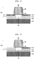
- FIG. 5 is a cross-sectional view illustrating a polysilicon gate TFT including source and drain regions implanted with lithium and connected between back-end-of-line (BEOL) metallization levels, according to an exemplary embodiment of the present invention.
- BEOL back-end-of-line
- FIG. 6 is a cross-sectional view illustrating a metal gate TFT including source and drain regions implanted with lithium and connected between BEOL metallization levels, according to an exemplary embodiment of the present invention.
- FIG. 7 is a cross-sectional view illustrating a polysilicon gate TFT including source and drain regions implanted with lithium and connected between BEOL metallization levels, according to an exemplary embodiment of the present invention.
- FIG. 8 is a cross-sectional view illustrating a metal gate TFT including source and drain regions implanted with lithium and connected between BEOL metallization levels, according to an exemplary embodiment of the present invention.
- FIG. 9 is a top layout view illustrating a polysilicon TFT on a back gate without a body contact connected to a channel region and including source and drain regions implanted with lithium, according to an exemplary embodiment of the present invention.
- FIG. 10 is a top layout view illustrating a polysilicon TFT on a back gate with a body contact connected to a channel region and including source and drain regions implanted with lithium, according to an exemplary embodiment of the present invention.
- FIG. 11 illustrates an array of lithium-doped field-effect transistor (FET) devices, according to an exemplary embodiment of the present invention.
- the semiconductor devices and methods for forming same in accordance with embodiments of the present invention can be employed in applications, hardware, and/or electronic systems.
- Suitable hardware and systems for implementing embodiments of the invention may include, but are not limited to, personal computers, communication networks, electronic commerce systems, portable communications devices (e.g., cell and smart phones), solid-state media storage devices, functional circuitry, etc.
- Systems and hardware incorporating the semiconductor devices are contemplated embodiments of the invention. Given the teachings of embodiments of the invention provided herein, one of ordinary skill in the art will be able to contemplate other implementations and applications of embodiments of the invention.
- the embodiments of the present invention can be used in connection with semiconductor devices that may require, for example, TFTs, FETs, CMOSs, MOSFETs, SETs, RPUs, PCMs, PMCs, PCRAMs, RRAMs and/or MRAMs.
- the semiconductor devices can include, but are not necessarily limited to TFT, FET, CMOS, MOSFET, SET, RPU, PCM, PMC, PCRAM, RRAM and/or MRAM devices, and/or semiconductor devices that use TFT, FET, CMOS, MOSFET, SET, RPU, PCM, PMC, PCRAM, RRAM and/or MRAM technology.
- “height” refers to a vertical size of an element (e.g., a layer, trench, hole, opening, etc.) in the cross-sectional views measured from a bottom surface to a top surface of the element, and/or measured with respect to a surface on which the element is located.
- a “depth” refers to a vertical size of an element (e.g., a layer, trench, hole, opening, etc.) in the cross-sectional views measured from a top surface to a bottom surface of the element. Terms such as “thick”, “thickness”, “thin” or derivatives thereof may be used in place of “height” where indicated.
- lateral refers to a side surface of an element (e.g., a layer, opening, etc.), such as a left or right side surface in the drawings.
- width or “length” refers to a size of an element (e.g., a layer, trench, hole, opening, etc.) in the drawings measured from a side surface to an opposite surface of the element. Terms such as “thick”, “thickness”, “thin” or derivatives thereof may be used in place of “width” or “length” where indicated.
- terms such as “on”, “overlying”, “atop”, “on top”, “positioned on” or “positioned atop” mean that a first element is present on a second element, wherein intervening elements may be present between the first element and the second element.
- the term “directly” used in connection with the terms “on”, “overlying”, “atop”, “on top”, “positioned on” or “positioned atop” or the term “direct contact” mean that a first element and a second element are connected without any intervening elements, such as, for example, intermediary conducting, insulating or semiconductor layers, present between the first element and the second element.
- a lithium-doped FET without a resistor is used in place of the resistive element.
- the state of the lithium-doped FET changes with an appropriate gate-source voltage (V gs ) or gate-drain voltage (V gd ).
- V gs gate-source voltage
- V gd gate-drain voltage
- a device incorporating an array of lithium-doped FETs will have a more linear response and consume much less power than the non-volatile resistive elements currently being used in RPU arrays.
- Lithium acts as an interstitial donor that compensates p-type doping and can be used to shift the threshold voltage and channel resistance controllably by drifting lithium ions in an applied field.
- Embodiments of the present invention utilize lithium-based FET arrays in the BEOL, which will reduce integration obstacles faced in the FEOL.
- the embodiments of the present invention also reduce the chip area by allowing other elements of the circuit to be built in the FEOL under the lithium-based FET arrays.
- Lithium drifted TFTs suitable for BEOL processing are described in more detail herein.
- BEOL refers to the part of integrated circuit (IC) fabrication where devices (e.g., transistors, capacitors, resistors, etc.) are interconnected with wiring (e.g., metallization levels/layers) on a wafer.
- BEOL portions of an IC can include, for example, contacts, dielectric layers, metallization levels and bonding sites.
- BEOL processes are performed after the FEOL processes and are carried out at lower temperatures (typically ⁇ 400° C.) so that the BEOL processes do not affect the properties of the devices fabricated in the FEOL.
- FIG. 1 is a cross-sectional view illustrating a polysilicon gate thin-film transistor (TFT) on a back gate and including a channel region implanted with lithium, according to an exemplary embodiment of the present invention.
- a TFT device 100 includes a channel layer 110 , which can be formed using, for example, known methods of thin film deposition and patterning.
- channels can comprise, for example, polycrystalline silicon or amorphous silicon (a-Si), germanium, poly-germanium or other semiconductor material, and are conducting channels that extend in a direction from a source to a drain.
- Lithium drift is faster in polysilicon than in other materials through defect-mediated transport, leading to faster write time; and (2) carrier mobility is much lower in polysilicon than in other materials, leading to higher channel resistance, which is a desired characteristic for RPU functionality.
- the on-resistance of a polysilicon TFT will be over 10 times higher for an equivalent x-Si FET.
- 14 M ⁇ to 84 M ⁇ RPU can be achieved by choosing appropriate channel geometry, polysilicon deposition conditions, device structure and operating bias point.
- epitaxial growth and/or deposition and “epitaxially formed and/or grown,” mean the growth of a semiconductor material (crystalline material) on a deposition surface of another semiconductor material (crystalline material), in which the semiconductor material being grown (crystalline over layer) has substantially the same crystalline characteristics as the semiconductor material of the deposition surface (seed material).
- the chemical reactants provided by the source gases are controlled, and the system parameters are set so that the depositing atoms arrive at the deposition surface of the semiconductor substrate with sufficient energy to move about on the surface such that the depositing atoms orient themselves to the crystal arrangement of the atoms of the deposition surface. Therefore, an epitaxially grown semiconductor material has substantially the same crystalline characteristics as the deposition surface on which the epitaxially grown material is formed.
- the epitaxial deposition process may employ the deposition chamber of a chemical vapor deposition type apparatus, such as a plasma-enhanced chemical vapor deposition (PECVD) apparatus.
- a chemical vapor deposition type apparatus such as a plasma-enhanced chemical vapor deposition (PECVD) apparatus.
- PECVD plasma-enhanced chemical vapor deposition
- a number of different sources may be used for the epitaxial deposition of the in situ doped semiconductor material.
- the gas source for the deposition of an epitaxially formed semiconductor material may include silicon (Si) deposited from silane, disilane, trisilane, tetrasilane, hexachlorodi silane, tetrachlorosilane, dichlorosilane, trichlorosilane, and combinations thereof.
- a germanium gas source may be selected from the group consisting of germane, digermane, halogermane, dichlorogermane, trichlorogermane, tetrachlorogermane and combinations thereof.
- the temperature for epitaxial deposition typically ranges from 450° C. to 900° C., but epitaxial growth at much lower temperatures has been demonstrated.
- perfect epitaxial growth is not a requirement, since the substrate material itself is polycrystalline. Although higher temperature typically results in faster deposition, the faster deposition may result in crystal defects and film cracking.
- in-situ it is meant that the dopant that dictates the conductivity type of the doped layer is introduced during the process step, e.g., epitaxial deposition, which forms the doped layer.
- lithium is introduced, for example, by a known implantation process, into the channel 110 , as shown by layer 120 so that an upper portion of the channel layer 110 , including a top surface of the channel layer 110 , (also referred to as “channel/gate dielectric interface”) includes lithium therein.
- Lithium ions are implanted at the channel/gate dielectric interface 120 .
- the implant energy can be adjusted to place the lithium atoms anywhere within the channel layer 110 or at the channel/dielectric interface 120 .
- the preference is to place the lithium atoms at or near the interface 120 where the operating electric fields are the highest.
- the motion of the lithium ions inside the gate dielectric layer 130 and at the channel/gate dielectric interface 120 has a significant impact on threshold voltage.
- the lithium can alternatively be introduced in source and/or drain regions.
- different biasing schemes can be employed to modulate the lithium concentration.
- Lithium concentration in the channel can vary from 1e16/cm 3 to 5e19/cm 3 .
- An alternative to polysilicon as a material for the channel 110 is poly-germanium (poly-Ge). Lithium drifts more easily in germanium than in silicon. Therefore, embodiments of the invention are also applicable to poly-Ge TFTs. If the source-drain regions are SiGe, then lithium may have a preference for that region, unless driven from the source-drain regions with an electric field during a write operation. Germanium may be used to control lithium drift.
- the gate dielectric layer 130 is formed on channel/gate dielectric interface 120 .
- the gate dielectric 130 includes, for example, silicon oxide (SiO x ) (x is, for example, 1.99, 2, 2.01), or other appropriate gate dielectric, such as HfO x or HFSiO x .
- a gate 140 is formed on the gate dielectric layer 130 and comprises, for example, polysilicon.
- the gate 140 can be deposited using a deposition technique including, but not necessarily limited to, chemical vapor deposition (CVD), PECVD, radio-frequency CVD (RFCVD), physical vapor deposition (PVD), atomic layer deposition (ALD), molecular beam deposition (MBD), pulsed laser deposition (PLD), and/or liquid source misted chemical deposition (LSMCD), sputtering, and/or plating.
- CVD chemical vapor deposition
- PECVD radio-frequency CVD
- PVD physical vapor deposition
- ALD atomic layer deposition
- MBD molecular beam deposition
- PLD pulsed laser deposition
- LSMCD liquid source misted chemical deposition
- Spacers 150 are formed adjacent to the gate 140 , to be in direct contact with opposing sidewalls of the gate 140 .
- the spacers 150 can include a dielectric insulating material such as, for example, SiO x , carbon doped silicon oxide (SiOC), silicon nitride (SiN), silicon oxynitride (SiON), carbon doped silicon oxynitride (SiOCN), boron nitride (BN), silicon boron nitride (SiBN), silicon boron carbon nitride (SiBCN) or multilayered stacks thereof.
- Source and drain regions 112 and 114 are formed adjacent to the spacers 150 and the channel layer 110 by low temperature epitaxial growth with in-situ doping or by dopant implantation.
- the source and drain regions 112 and 114 may comprise semiconductor material including, but not limited to, Si, SiGe, SiC, SiGeC or other like semiconductor with dopants, such as, boron, phosphorus, arsenic and any other applicable elements.
- the TFT device 100 is fabricated in the BEOL using low temperature (e.g., ⁇ 400° C.) processes.
- the TFT is optionally formed on and/or electronically connected to a back gate 102 comprising, for example, a conductive metal, such as, for example, copper, tungsten (W), titanium (Ti), ruthenium (Ru), cobalt (Co), titanium nitride (TiN), or combinations thereof, which is connected to a metallization layer.
- a thin dielectric layer 104 comprising, for example, silicon nitride (SiN), silicon carbon nitride (SiCN), HFO x , HFSiO x or silicon nitrided oxide (SiNO) is formed on the back gate 102 .
- a thickness of the dielectric layer 104 is in the range of about 10 angstroms to about 100 angstroms.
- the TFT device 100 and the back gate and dielectric 102 and 104 which are formed at the BEOL, may be formed on a semiconductor substrate (not shown), with intervening layers (e.g., lower conductive lines, transistors, capacitors, resistors, other devices, etc.) between the back gate 102 or TFT device 100 and the substrate.
- a semiconductor substrate may comprise semiconductor material including, but not limited to, Si, SiGe, SiC, SiGeC or other like semiconductor.
- multiple layers of the semiconductor materials can be used as the semiconductor material of the substrate.
- a plurality of devices can be on the substrate, such as, for example, transistors, capacitors, and resistors.
- FIG. 2 is a cross-sectional view illustrating a polysilicon gate TFT on a back gate and including source and drain regions implanted with lithium, according to an exemplary embodiment of the present invention.
- a TFT device 200 includes a channel layer 210 similar to the channel layer 110 described in connection with FIG. 1 . Unlike the channel layer 110 , the channel layer 210 is not implanted with lithium.
- elements in FIG. 2 with similar reference numbers to those in FIG. 1 have the same or similar structure as those elements in FIG. 1 , and for the sake of brevity, duplicative descriptions of those elements are omitted.
- a gate dielectric layer 230 including the same or similar material and structure as the gate dielectric layer 130 is formed on channel 210 .
- a gate 240 including the same or similar material and structure as the gate 140 is formed on the gate dielectric layer 230 .
- Spacers 250 including the same or similar material and structure as the spacers 150 are formed adjacent to the gate 240 , to be in direct contact with opposing sidewalls of the gate 240 .
- Source and drain regions 212 and 214 are formed adjacent to the spacers 250 and the channel layer 210 by low temperature epitaxial growth with in-situ doping or by dopant implantation.
- the source and drain regions 212 and 214 may comprise semiconductor material including, but not limited to, Si, SiGe, SiC, SiGeC or other like semiconductor with dopants, such as, boron, phosphorus, arsenic and any other applicable elements.
- lithium is introduced, for example, by a known implantation process, in the source and drain regions 212 and 214 , respectively, as shown by layers 222 and 224 so that upper portions of the source and drain regions 212 and 214 , including top surfaces of the source and drain regions 212 and 214 , include lithium therein.
- the source and drain regions 212 and 214 are generally very heavily doped, so the lithium concentration in these regions can be in the range of about 1e16/cm 3 -about 1e19/cm 3 without impacting the source-drain doping levels.
- the lithium implant is done at a slight angle to position the lithium closer to the junction edges of the source and drain regions.
- the depth of the lithium implant will be less than the depth of the source and drain regions 212 and 214 (e.g., about 10 nm-about 100 nm), and adjacent to the channel.
- the TFT device 200 is fabricated in the BEOL using low temperature (e.g., ⁇ 400° C.) processes, and is optionally formed on and/or electronically connected to a back gate 202 comprising a thin dielectric layer 204 formed thereon.
- the back gate and thin dielectric layer 202 and 204 include the same or similar material and structure as the back gate and thin dielectric layer 102 and 104 .
- the TFT device 200 and the back gate and dielectric 202 and 204 which are formed at the BEOL, may be formed on a semiconductor substrate.
- FIG. 3 is a cross-sectional view illustrating a polysilicon gate TFT on a back gate and including a drain region implanted with lithium, according to an exemplary embodiment of the present invention.
- a TFT device 300 includes a channel layer 310 similar to the channel layer 210 described in connection with FIG. 2 .
- elements in FIG. 3 with similar reference numbers to those in FIG. 1 or 2 have the same or similar structure as those elements in FIG. 1 or 2 , and for the sake of brevity, duplicative descriptions of those elements are omitted.
- the channel layer 310 is not implanted with lithium.
- a gate dielectric layer 330 including the same or similar material and structure as the gate dielectric layer 130 or 230 is formed on channel 310 .
- a gate 340 including the same or similar material and structure as the gate 140 or 240 is formed on the gate dielectric layer 330 .
- Spacers 350 including the same or similar material and structure as the spacers 150 or 250 are formed adjacent to the gate 340 , to be in direct contact with opposing sidewalls of the gate 340 .
- Source and drain regions 312 and 314 are formed adjacent to the spacers 350 and the channel layer 310 by low temperature epitaxial growth with in-situ doping or by dopant implantation.
- the source and drain regions 312 and 314 may comprise semiconductor material including, but not limited to, Si, SiGe, SiC, SiGeC or other like semiconductor with dopants, such as, boron, phosphorus, arsenic and any other applicable elements.
- lithium is introduced, for example, by a known implantation process, in the drain region 314 , as shown by layer 324 so that an upper portion of the drain region 314 , including a top surface of the drain region 314 , includes lithium therein.
- the source and drain regions 312 and 314 are generally very heavily doped, so the lithium concentration in the drain region 314 can be in the range of about 1e16/cm 3 -about 1e19/cm 3 without impacting the drain doping level.
- the lithium implant is done at a slight angle to position the lithium closer to the junction edge of the drain region 314 , adjacent to the channel.
- the depth of the lithium implant will be approximately the depth of the drain region 314 (e.g., about 10 nm-about 100 nm).
- the source region 312 is not implanted with lithium.
- the TFT device 300 is fabricated in the BEOL using low temperature (e.g., ⁇ 400° C.) processes, and is optionally formed on and/or electronically connected to a back gate 302 comprising a thin dielectric layer 304 formed thereon.
- the back gate and thin dielectric layer 302 and 304 include the same or similar material and structure as the back gate and thin dielectric layer 102 and 104 or 202 and 204 .
- the TFT device 300 and the back gate and dielectric 302 and 304 which are formed at the BEOL, may be formed on a semiconductor substrate.
- FIGS. 4A and 4B are graphs of drain current (Id) and log of the drain current log(Id), respectively, versus gate voltage (Vg).
- the graphs 401 and 403 illustrate threshold voltage change due to lithium drift, according to an exemplary embodiment of the present invention.
- the threshold voltage may gradually increase. For example, forward and backward passes are read operations and are preferably performed with as low voltages as possible to avoid unintentional drift of lithium.
- the source-drain can be biased in the linear regime (typically ⁇ 100 mV), and the gate (V g,read ) can be biased somewhat above the unshifted threshold voltage (V to ), to allow for minimum disturbance and high channel resistance.
- Weight updates are done using stochastic bit streams, which can be applied to the gate-source, gate-substrate (if available) or source-drain.
- Gate-substrate may be the preferred method, since it effectively decouples the read and write operations (i.e., gate-substrate moves lithium orthogonal to direction of source-drain bias).
- Up-down conductance response is expected to be symmetric since lithium drift can be reversed by applying opposite polarity.
- Source-drain bias disturbance can be minimized by using low drain to Vds (source-drain bias) and by using symmetric AC bias.
- lithium can be introduced in the source and/or drain, or in the channel.
- different biasing schemes can be employed to modulate the lithium concentration.
- TFTs having lithium implanted portions can be integrated into the BEOL.
- the lithium based TFTs can be integrated into the BEOL between two metal interconnect layers Mx and MxPlus in multiple ways.
- FIGS. 5 and 7 show two embodiments for polysilicon gate FETs and FIGS. 6 and 8 show two embodiments for metal gate TFTs.
- the devices can be integrated by building a metal pedestal as the back gate of the TFT and then building the TFT on top of the metal pedestal.
- FIG. 5 is a cross-sectional view illustrating a polysilicon gate TFT including source and drain regions implanted with lithium and connected between BEOL metallization levels, according to an exemplary embodiment of the present invention.
- a device 500 includes a TFT similar to the TFT 200 shown in FIG. 2 .
- the TFT in FIG. 5 includes channel layer 510 similar to the channel layer 210 described in connection with FIG. 2 .
- elements in FIG. 5 with similar reference numbers to those in FIG. 2 have the same or similar structure as those elements in FIG. 2 , and for the sake of brevity, duplicative descriptions of those elements are omitted.
- a gate dielectric layer 530 including the same or similar material and structure as the gate dielectric layer 230 is formed on channel 510 .
- a gate 540 including the same or similar material and structure as the gate 240 is formed on the gate dielectric layer 530 .
- Spacers 550 including the same or similar material and structure as the spacers 250 are formed adjacent to the gate 540 , to be in direct contact with opposing sidewalls of the gate 540 .
- Source and drain regions 512 and 514 are formed adjacent to the spacers 550 and the channel layer 510 by low temperature epitaxial growth with in-situ doping or by dopant implantation.
- the source and drain regions 512 and 514 may comprise semiconductor material including, but not limited to, Si, SiGe, SiC, SiGeC or other like semiconductor with dopants, such as, boron, phosphorus, arsenic and any other applicable elements.
- lithium is introduced, for example, by a known implantation process, in the source and drain regions 512 and 514 , respectively, as shown by layers 522 and 524 .
- the TFT device in FIG. 5 is formed on and/or electronically connected to a back gate 502 comprising a thin dielectric layer 504 formed thereon.
- the back gate and thin dielectric layer 502 and 504 include the same or similar material and structure as the back gate and thin dielectric layer 202 and 204 .
- Contacts to the source 512 , drain 514 and gate 540 are made using, for example, vias 562 and 564 that connect to metal contacts 572 , 574 in an upper metal interconnect layer MxPlus of the BEOL.
- the back gate 502 in FIG. 5 is formed on and electrically connected to a metal contact 580 of a lower metal interconnect layer Mx of the BEOL.
- the 2 metal interconnect layers (Mx and MxPlus) can be consecutive metal layers of the BEOL (example M 2 and M 3 ) or 2 metal interconnect layers that are separated by one or more metal interconnect layers (example M 2 and M 4 ), if more height is needed to accommodate the TFT. Accordingly, for Mx, x can be an integer greater than or equal to 0, while for MxPlus, xPlus is an integer greater than the value of x.
- the vias 562 and 564 contact the layers 522 and 524 on the source and drain regions 512 and 522 .
- the vias 562 and 564 each comprise, for example, a conductive metal formed in a trench through a dielectric layer (not shown).
- the metal contacts 572 , 574 and 580 also comprise a conductive metal.
- the conductive metal of the vias 562 and 564 and of metal contacts 572 , 574 and 580 can include, but is not necessarily limited to, W, Ti, Ru, Co, TiN or other conductive metal or alloys thereof.
- FIG. 6 is a cross-sectional view illustrating a metal gate TFT including source and drain regions implanted with lithium and connected between BEOL metallization levels, according to an exemplary embodiment of the present invention.
- a device 600 includes a TFT similar to the TFT 500 shown in FIG. 5 , with some exceptions.
- the TFT in FIG. 6 is a metal gate TFT, not a polysilicon gate TFT.
- the metal gate 645 includes a conductive metal, including, but not necessarily limited to, W, Ti, Ru, Co, TiN or other conductive metal or alloys thereof.
- the TFT in FIG. 6 includes channel layer 610 similar to the channel layer 510 described in connection with FIG. 5 .
- elements in FIG. 6 with similar reference numbers to those in FIG. 5 have the same or similar structure as those elements in FIG. 5 , and for the sake of brevity, duplicative descriptions of those elements are omitted.
- a gate dielectric layer 635 is formed on the channel 610 and on source and drain regions 612 and 614 including the lithium implanted layers 622 and 624 thereon.
- the gate dielectric 635 includes, for example, SiO x or other appropriate gate dielectric
- the metal gate 645 is formed on a portion of the gate dielectric layer 635 over the channel 610 and over portions of the lithium implanted layers 622 and 624 adjacent the channel 610 . Unlike the polysilicon gate TFTs, there are no spacers around the metal gate 645 .
- the source and drain regions 612 and 614 are formed adjacent to the channel layer 610 by low temperature epitaxial growth with in-situ doping or by dopant implantation.
- the source and drain regions 612 and 614 may comprise semiconductor material including, but not limited to, Si, SiGe, SiC, SiGeC or other like semiconductor with dopants, such as, boron, phosphorus, arsenic and any other applicable elements.
- dopants such as, boron, phosphorus, arsenic and any other applicable elements.
- lithium is introduced, for example, by a known implantation process, in the source and drain regions 612 and 614 , respectively, as shown by layers 622 and 624 .
- the TFT device in FIG. 6 is formed on and/or electronically connected to a back gate 602 comprising a thin dielectric layer 604 formed thereon.
- the back gate and thin dielectric layer 602 and 604 include the same or similar material and structure as the back gate and thin dielectric layer 502 and 504 .
- Contacts to the source 612 , drain 614 and gate 645 are made using, for example, vias 662 and 664 that connect to metal contacts 672 , 674 in an upper metal interconnect layer MxPlus of the BEOL.
- the back gate 602 in FIG. 6 is formed on and electrically connected to a metal contact 680 of a lower metal interconnect layer Mx of the BEOL.
- the vias 662 and 664 are formed through the gate dielectric layer 635 to contact the layers 622 and 624 on the source and drain regions 612 and 622 .
- the vias 662 and 664 each comprise, for example, a conductive metal formed in a trench through a dielectric layer (not shown).
- the metal contacts 672 , 674 and 680 also comprise a conductive metal.
- the conductive metal of the vias 662 and 664 and of metal contacts 672 , 674 and 580 can include, but is not necessarily limited to, W, Ti, Ru, Co, TiN or other conductive metal or alloys thereof.
- FIG. 7 is a cross-sectional view illustrating a polysilicon gate TFT including source and drain regions implanted with lithium and connected between BEOL metallization levels, according to an exemplary embodiment of the present invention.
- a device 700 includes a TFT similar to the TFT 200 shown in FIG. 2 .
- the TFT in FIG. 7 includes channel layer 710 similar to the channel layer 210 described in connection with FIG. 2 .
- elements in FIG. 7 with similar reference numbers to those in FIG. 2 have the same or similar structure as those elements in FIG. 2 , and for the sake of brevity, duplicative descriptions of those elements are omitted.
- a gate dielectric layer 730 including the same or similar material and structure as the gate dielectric layer 230 is formed on channel 710 .
- a gate 740 including the same or similar material and structure as the gate 240 is formed on the gate dielectric layer 730 .
- Spacers 750 including the same or similar material and structure as the spacers 250 are formed adjacent to the gate 740 , to be in direct contact with opposing sidewalls of the gate 740 .
- Source and drain regions 712 and 714 are formed adjacent to the spacers 750 and the channel layer 710 by low temperature epitaxial growth with in-situ doping or by dopant implantation.
- the source and drain regions 712 and 714 may comprise semiconductor material including, but not limited to, Si, SiGe, SiC, SiGeC or other like semiconductor with dopants, such as, boron, phosphorus, arsenic and any other applicable elements.
- lithium is introduced, for example, by a known implantation process, in the source and drain regions 712 and 714 , respectively, as shown by layers 722 and 724 .
- the TFT device in FIG. 7 is formed on and/or electronically connected to a back gate 702 comprising a thin dielectric layer 704 formed thereon.
- the back gate and thin dielectric layer 702 and 704 include the same or similar material and structure as the back gate and thin dielectric layer 202 and 204 .
- contacts to the source 712 , drain 714 and gate 740 are made using, for example, vias 762 and 764 that connect to metal contacts 772 , 774 in an upper metal interconnect layer MxPlus of the BEOL.
- the vias 762 and 764 contact the layers 722 and 724 on the source and drain regions 712 and 722 .
- the back gate 702 in FIG. 7 is electrically connected to a metal contact 780 of a lower metal interconnect layer Mx of the BEOL by a via 785 .
- the back gate 702 is spaced apart from and connected to the lower metal interconnect layer with the via 785 so that there may be easier integration and less impact on the POR BEOL process than the embodiment in FIG. 5 .
- the vias 762 , 764 and 785 each comprise, for example, a conductive metal formed in a trench through a dielectric layer (not shown).
- the metal contacts 772 , 774 and 780 also comprise a conductive metal.
- the conductive metal of the vias 762 , 764 and 785 and of metal contacts 772 , 774 and 780 can include, but is not necessarily limited to, W, Ti, Ru, Co, TiN or other conductive metal or alloys thereof.
- FIG. 8 is a cross-sectional view illustrating a metal gate TFT including source and drain regions implanted with lithium and connected between BEOL metallization levels, according to an exemplary embodiment of the present invention.
- a device 800 includes a TFT similar to the TFT 600 shown in FIG. 6 .
- the TFT in FIG. 8 is a metal gate TFT.
- the metal gate 845 includes a conductive metal, including, but not necessarily limited to, W, Ti, Ru, Co, TiN or other conductive metal or alloys thereof.
- the TFT in FIG. 8 includes channel layer 810 similar to the channel layer 610 described in connection with FIG. 6 .
- elements in FIG. 8 with similar reference numbers to those in FIG. 6 have the same or similar structure as those elements in FIG. 6 , and for the sake of brevity, duplicative descriptions of those elements are omitted.
- a gate dielectric layer 835 is formed on the channel 810 and on source and drain regions 812 and 814 including the lithium implanted layers 822 and 824 thereon.
- the metal gate 845 is formed on a portion of the gate dielectric layer 835 over the channel 810 and over portions of the lithium implanted layers 822 and 824 adjacent the channel 810 .
- the TFT device in FIG. 8 is formed on and/or electronically connected to a back gate 802 comprising a thin dielectric layer 804 formed thereon.
- the back gate and thin dielectric layer 802 and 804 include the same or similar material and structure as the back gate and thin dielectric layer 602 and 604 .
- contacts to the source 812 , drain 814 and gate 845 are made using, for example, vias 862 and 864 that connect to metal contacts 872 , 874 in an upper metal interconnect layer MxPlus of the BEOL.
- the back gate 802 in FIG. 8 is electrically connected to a metal contact 880 of a lower metal interconnect layer Mx of the BEOL by a via 885 .
- the back gate 802 is spaced apart from and connected to the lower metal interconnect layer with the via 885 so that there may be easier integration and less impact on the POR BEOL process than the embodiment in FIG. 6 .
- the vias 862 and 864 are formed through the gate dielectric layer 835 to contact the layers 822 and 824 on the source and drain regions 812 and 814 .
- the vias 862 , 864 and 885 each comprise, for example, a conductive metal formed in a trench through a dielectric layer (not shown).
- the metal contacts 872 , 874 and 880 also comprise a conductive metal.
- the conductive metal of the vias 862 , 864 and 885 and of metal contacts 872 , 874 and 880 can include, but is not necessarily limited to, W, Ti, Ru, Co, TiN or other conductive metal or alloys thereof.
- FIGS. 9 and 10 are top layout views illustrating a polysilicon TFT on a back gate without a body contact connected to a channel region, and a polysilicon TFT on a back gate with a body contact connected to a channel region, respectively.
- the TFTs of FIGS. 9 and 10 include source and drain regions implanted with lithium, according to exemplary embodiments of the present invention.
- the devices 900 and 1000 each include a TFT similar to the TFTs 500 and 700 shown in FIGS. 5 and 7 .
- elements in FIGS. 9 and 10 with similar reference numbers to those in FIGS. 5 and 7 have the same or similar structure as those elements in FIGS.
- Layouts similar to those shown in FIGS. 9 and 10 may also be applied to devices with metal gate TFTs similar to the TFTs 600 and 800 shown in FIGS. 6 and 8 .
- Gates 940 and 1040 including the same or similar material and structure as the gates 540 and 740 are formed on a gate dielectric layer (not shown) over a channel layer (not shown). Source and drain regions are formed adjacent to the channel layer. Lithium is introduced, for example, by a known implantation process, in the source and drain regions, respectively, as shown by elements 922 / 1022 and 924 / 1024 .
- the TFT devices in FIGS. 9 and 10 are formed on and/or electronically connected to back gates comprising a thin dielectric layer 904 / 1004 formed thereon.
- the back gates and thin dielectric layers 904 / 1004 include the same or similar material and structure as the back gate and thin dielectric layers 502 , 702 and 504 , 704 .
- Contacts to the sources, drains and gates 940 / 1040 are made using, for example, vias 962 / 1062 , 964 / 1064 and 969 / 1069 that connect to metal contacts in an upper metal interconnect layer MxPlus of the BEOL.
- the vias 962 / 1062 and 964 / 1064 contact the layers 922 / 1022 and 924 / 1024 on the source and drain regions.
- a contact to the back gate is made using, for example, a via 967 / 1067 formed through the dielectric layer 904 / 1004 that connects to a metal contact in the upper metal interconnect layer MxPlus of the BEOL.
- the back gate can be formed on or electrically connected with a via to a metal contact of a lower metal interconnect layer Mx of the BEOL.
- the device 1000 includes a body contact 1090 connected to a channel region (not shown).
- An electrical connection to the body contact 1090 is made using, for example, a via 1092 that connects to a metal contact in the upper metal interconnect layer MxPlus of the BEOL.
- FIG. 11 illustrates an array of lithium-doped field-effect transistor (FET) devices, according to an exemplary embodiment of the present invention.
- the array 1100 of lithium-doped FETs 1110 includes a plurality front gate voltage lines G, a plurality of source voltage lines S, a plurality of drain voltage lines D and a plurality of optional back gate voltage lines X.
- the front gate lines and back gate lines are connected to upper metallization level MxPlus or higher. If there are no back gates, the back gate voltage lines can be omitted.
- Weight update operations can be performed using stochastic bit streams relying on a variety of different possible combinations, such as, for example, gate-substrate, gate-source, or source-drain. Using gate-substrate for write operations decouples write from read (source-drain).
- Each of the FETs 1110 in the array 1100 can have one or a combination of the structures described in connection with FIGS. 1-3 and 5-10 described herein.
- embodiments of the present invention provide for use of lithium drift in a TFT structure to achieve an RPU element in the BEOL without having any impact on the FEOL.
- the embodiments are easily and inexpensively integrated into POR CMOS processes, and provide for symmetric response (e.g., drift can be reversed by applying opposite polarity).
- RPUs are enabled with multi-state FETs that change their states based on lithium motion. The resulting change in threshold voltage leads to a change in resistance of the FET itself.
- the length of metal lines in connection with TFT structures being used as RPUs is limited by the frequency of operation. For example, an estimated length is approximately 1.6 mm for a 1 GHz design.
- a BEOL array greatly reduces this length, as the active circuitry can be placed below the array and the metal layers above and below a magnetic tunnel junction (MTJ) can be used for wiring.
- Chip area is also reduced as active circuit elements can be placed in the FEOL below the array, and a transistor crosspoint cell can be produced with a smaller overall chip area.
- MTJ magnetic tunnel junction
- Embodiments of the present invention provide for a large number of possible states since lithium can be incrementally drifted to give small threshold voltage shifts.
- RPU element resistance range can be modulated through gate bias, read and write operations can be decoupled through substrate or back gate contact, and minimal read disturbance can be achieved by low-voltage symmetric AC source-drain bias.
- Embodiments of the present invention also provide non-volatility (assuming no thermal diffusion of lithium at operating conditions), and increased reliability due to the ability to confine lithium silicon, germanium or other channel material by using barrier layers.
Abstract
Description
Claims (14)
Priority Applications (1)
| Application Number | Priority Date | Filing Date | Title |
|---|---|---|---|
| US16/217,651 US11444207B2 (en) | 2018-12-12 | 2018-12-12 | Lithium drifted thin film transistors for neuromorphic computing |
Applications Claiming Priority (1)
| Application Number | Priority Date | Filing Date | Title |
|---|---|---|---|
| US16/217,651 US11444207B2 (en) | 2018-12-12 | 2018-12-12 | Lithium drifted thin film transistors for neuromorphic computing |
Publications (2)
| Publication Number | Publication Date |
|---|---|
| US20200194597A1 US20200194597A1 (en) | 2020-06-18 |
| US11444207B2 true US11444207B2 (en) | 2022-09-13 |
Family
ID=71072986
Family Applications (1)
| Application Number | Title | Priority Date | Filing Date |
|---|---|---|---|
| US16/217,651 Active 2039-10-30 US11444207B2 (en) | 2018-12-12 | 2018-12-12 | Lithium drifted thin film transistors for neuromorphic computing |
Country Status (1)
| Country | Link |
|---|---|
| US (1) | US11444207B2 (en) |
Citations (14)
| Publication number | Priority date | Publication date | Assignee | Title |
|---|---|---|---|---|
| US20010045578A1 (en) * | 2000-05-20 | 2001-11-29 | Hueting Raymond J.E. | Semiconductor device |
| JP4482228B2 (en) | 1998-04-09 | 2010-06-16 | カリフォルニア・インスティテュート・オブ・テクノロジー | Electronic technology for analyte detection |
| JP2012119577A (en) | 2010-12-02 | 2012-06-21 | Renesas Electronics Corp | Semiconductor chip, semiconductor device, and method of manufacturing semiconductor chip |
| US20120284217A1 (en) | 2009-11-18 | 2012-11-08 | International Business Machines Corporation | Area efficient neuromorphic system |
| US20130049092A1 (en) * | 2011-08-22 | 2013-02-28 | Qingqing Liang | Semiconductor device |
| US20150221648A1 (en) * | 2014-01-31 | 2015-08-06 | Stmicroelectronics, Inc. | High dose implantation for ultrathin semiconductor-on-insulator substrates |
| US20160172527A1 (en) * | 2012-12-03 | 2016-06-16 | Sandia Corporation | Photodetector with Interdigitated Nanoelectrode Grating Antenna |
| US20160268418A1 (en) | 2013-07-29 | 2016-09-15 | Samsung Electronics Co., Ltd. | Nonvolatile memory transistor and device including the same |
| US20160350643A1 (en) | 2015-05-26 | 2016-12-01 | International Business Machines Corporation | Neuron peripheral circuits for neuromorphic synaptic memory array based on neuron models |
| US9553056B1 (en) * | 2015-10-27 | 2017-01-24 | International Business Machines Corporation | Semiconductor chip having tampering feature |
| US20170109626A1 (en) | 2015-10-20 | 2017-04-20 | International Business Machines Corporation | Resistive processing unit |
| US20170194337A1 (en) | 2015-12-30 | 2017-07-06 | SK Hynix Inc. | Neuromorphic device |
| US9852790B1 (en) * | 2016-10-26 | 2017-12-26 | International Business Machines Corporation | Circuit methodology for highly linear and symmetric resistive processing unit |
| US20190096886A1 (en) * | 2017-09-28 | 2019-03-28 | Taiwan Semiconductor Manufacturing Co., Ltd. | Embedded semiconductor region for latch-up susceptibility improvement |
-
2018
- 2018-12-12 US US16/217,651 patent/US11444207B2/en active Active
Patent Citations (15)
| Publication number | Priority date | Publication date | Assignee | Title |
|---|---|---|---|---|
| JP4482228B2 (en) | 1998-04-09 | 2010-06-16 | カリフォルニア・インスティテュート・オブ・テクノロジー | Electronic technology for analyte detection |
| US20010045578A1 (en) * | 2000-05-20 | 2001-11-29 | Hueting Raymond J.E. | Semiconductor device |
| US20120284217A1 (en) | 2009-11-18 | 2012-11-08 | International Business Machines Corporation | Area efficient neuromorphic system |
| US8589320B2 (en) | 2009-11-18 | 2013-11-19 | International Business Machines Corporation | Area efficient neuromorphic system that connects a FET in a diode configuration, and a variable resistance material to junctions of neuron circuit blocks |
| JP2012119577A (en) | 2010-12-02 | 2012-06-21 | Renesas Electronics Corp | Semiconductor chip, semiconductor device, and method of manufacturing semiconductor chip |
| US20130049092A1 (en) * | 2011-08-22 | 2013-02-28 | Qingqing Liang | Semiconductor device |
| US20160172527A1 (en) * | 2012-12-03 | 2016-06-16 | Sandia Corporation | Photodetector with Interdigitated Nanoelectrode Grating Antenna |
| US20160268418A1 (en) | 2013-07-29 | 2016-09-15 | Samsung Electronics Co., Ltd. | Nonvolatile memory transistor and device including the same |
| US20150221648A1 (en) * | 2014-01-31 | 2015-08-06 | Stmicroelectronics, Inc. | High dose implantation for ultrathin semiconductor-on-insulator substrates |
| US20160350643A1 (en) | 2015-05-26 | 2016-12-01 | International Business Machines Corporation | Neuron peripheral circuits for neuromorphic synaptic memory array based on neuron models |
| US20170109626A1 (en) | 2015-10-20 | 2017-04-20 | International Business Machines Corporation | Resistive processing unit |
| US9553056B1 (en) * | 2015-10-27 | 2017-01-24 | International Business Machines Corporation | Semiconductor chip having tampering feature |
| US20170194337A1 (en) | 2015-12-30 | 2017-07-06 | SK Hynix Inc. | Neuromorphic device |
| US9852790B1 (en) * | 2016-10-26 | 2017-12-26 | International Business Machines Corporation | Circuit methodology for highly linear and symmetric resistive processing unit |
| US20190096886A1 (en) * | 2017-09-28 | 2019-03-28 | Taiwan Semiconductor Manufacturing Co., Ltd. | Embedded semiconductor region for latch-up susceptibility improvement |
Non-Patent Citations (8)
| Title |
|---|
| C.-H. Tseng et al., "Effects of Excimer Laser Dopant Activation on Low Temperature Polysilicon Thin-Film Transistors with Lightly Doped Drains," Electrochemical and Solid-State Letters, Jul. 12, 2001, pp. G94-G97, vol. 4, No. 11. |
| David Cardinal, "Resistive Computing: Based on the Human Brain," PC Magazine Digital Edition, May 2016, 6 pages. |
| G. Adamopoulos et al., "High-Mobility Low-Voltage ZnO and Li-Doped ZnO Transistors Based on ZrO2 High-k Dielectric Grown by Spray Pyrolysis in Ambient Air," Advanced Materials, Apr. 26, 2011, pp. 1894-1898, vol. 23, No. 16. |
| http://en.wikipedia.org/wiki/Neuromophic_engineering, Oct. 18, 2018, 5 pages. |
| M. Xu et al., "A High Performance InGaZnO Thin-Film Transistors Integrated Amplifier Circuit for Capacitance Sensing," IEEE Transactions on Circuits and Systems II: Express Briefs, Jun. 2018, pp. 734-738, vol. 65, No. 6. |
| T. Gokmen et al., "Acceleration of Deep Neural Network Training with Resistive Cross-Point Devices," Frontiers in Neuroscience, Jul. 21, 2016, 19 pages. |
| Von K. Steinbuch, Die Lernmatrix, Kybernetik, (1961), pp. 36-45, vol. 1. |
| Wenhui Wan et al., "First principles study of lithium insertion in bulk silicon," Journal of Physics Condensed Matter, 2010, 9 pages, vol. 22. |
Also Published As
| Publication number | Publication date |
|---|---|
| US20200194597A1 (en) | 2020-06-18 |
Similar Documents
| Publication | Publication Date | Title |
|---|---|---|
| US11309492B2 (en) | Multi-layer structure to increase crystalline temperature of a selector device | |
| US6404665B1 (en) | Compositionally modified resistive electrode | |
| US7495337B2 (en) | Dual-gate device and method | |
| US11901356B2 (en) | Three-dimensional semiconductor devices | |
| US11195879B2 (en) | Method and related apparatus for improving memory cell performance in semiconductor-on-insulator technology | |
| US10937911B2 (en) | Method of forming a transistor | |
| WO2018182799A1 (en) | Methods and apparatus for three-dimensional non-volatile memory | |
| US20090191680A1 (en) | Dual-gate memory device with channel crystallization for multiple levels per cell (mlc) | |
| US11869803B2 (en) | Single crystalline silicon stack formation and bonding to a CMOS wafer | |
| US11455521B2 (en) | Neuromorphic device driven by copper ion intercalation | |
| US11444207B2 (en) | Lithium drifted thin film transistors for neuromorphic computing | |
| US10741754B2 (en) | Resistive memory with amorphous silicon filaments | |
| CN111247641B (en) | High resistance sense FET for cognitive devices | |
| US9087576B1 (en) | Low temperature fabrication method for a three-dimensional memory device and structure | |
| US20210399047A1 (en) | Heterojunction thin film diode | |
| US9153623B1 (en) | Thin film transistor steering element for a non-volatile memory device | |
| KR20220115070A (en) | Thin film transistor including a dielectric diffusion barrier and methods for forming the same |
Legal Events
| Date | Code | Title | Description |
|---|---|---|---|
| AS | Assignment |
Owner name: INTERNATIONAL BUSINESS MACHINES CORPORATION, NEW YORK Free format text: ASSIGNMENT OF ASSIGNORS INTEREST;ASSIGNORS:KHAN, BABAR;LI, NING;KUMAR, ARVIND;AND OTHERS;SIGNING DATES FROM 20181205 TO 20181211;REEL/FRAME:047756/0009 |
|
| FEPP | Fee payment procedure |
Free format text: ENTITY STATUS SET TO UNDISCOUNTED (ORIGINAL EVENT CODE: BIG.); ENTITY STATUS OF PATENT OWNER: LARGE ENTITY |
|
| STPP | Information on status: patent application and granting procedure in general |
Free format text: RESPONSE TO NON-FINAL OFFICE ACTION ENTERED AND FORWARDED TO EXAMINER |
|
| STPP | Information on status: patent application and granting procedure in general |
Free format text: NON FINAL ACTION MAILED |
|
| STPP | Information on status: patent application and granting procedure in general |
Free format text: RESPONSE TO NON-FINAL OFFICE ACTION ENTERED AND FORWARDED TO EXAMINER |
|
| STPP | Information on status: patent application and granting procedure in general |
Free format text: FINAL REJECTION MAILED |
|
| STPP | Information on status: patent application and granting procedure in general |
Free format text: ADVISORY ACTION MAILED |
|
| STPP | Information on status: patent application and granting procedure in general |
Free format text: DOCKETED NEW CASE - READY FOR EXAMINATION |
|
| STPP | Information on status: patent application and granting procedure in general |
Free format text: NON FINAL ACTION MAILED |
|
| STPP | Information on status: patent application and granting procedure in general |
Free format text: RESPONSE TO NON-FINAL OFFICE ACTION ENTERED AND FORWARDED TO EXAMINER |
|
| STPP | Information on status: patent application and granting procedure in general |
Free format text: NOTICE OF ALLOWANCE MAILED -- APPLICATION RECEIVED IN OFFICE OF PUBLICATIONS |
|
| STPP | Information on status: patent application and granting procedure in general |
Free format text: PUBLICATIONS -- ISSUE FEE PAYMENT RECEIVED |
|
| STPP | Information on status: patent application and granting procedure in general |
Free format text: PUBLICATIONS -- ISSUE FEE PAYMENT VERIFIED |
|
| STCF | Information on status: patent grant |
Free format text: PATENTED CASE |