US11442301B2 - Display device - Google Patents
Display device Download PDFInfo
- Publication number
- US11442301B2 US11442301B2 US16/741,090 US202016741090A US11442301B2 US 11442301 B2 US11442301 B2 US 11442301B2 US 202016741090 A US202016741090 A US 202016741090A US 11442301 B2 US11442301 B2 US 11442301B2
- Authority
- US
- United States
- Prior art keywords
- support piece
- support
- display
- display unit
- display device
- Prior art date
- Legal status (The legal status is an assumption and is not a legal conclusion. Google has not performed a legal analysis and makes no representation as to the accuracy of the status listed.)
- Active, expires
Links
- 230000005484 gravity Effects 0.000 claims description 25
- 239000012790 adhesive layer Substances 0.000 abstract description 13
- 210000004027 cell Anatomy 0.000 description 34
- 230000004048 modification Effects 0.000 description 14
- 238000012986 modification Methods 0.000 description 14
- 238000005452 bending Methods 0.000 description 10
- 239000004973 liquid crystal related substance Substances 0.000 description 7
- 230000001133 acceleration Effects 0.000 description 5
- 239000011521 glass Substances 0.000 description 5
- 125000006850 spacer group Chemical group 0.000 description 5
- 239000000853 adhesive Substances 0.000 description 3
- 230000001070 adhesive effect Effects 0.000 description 3
- 210000002858 crystal cell Anatomy 0.000 description 3
- NIXOWILDQLNWCW-UHFFFAOYSA-N acrylic acid group Chemical group C(C=C)(=O)O NIXOWILDQLNWCW-UHFFFAOYSA-N 0.000 description 2
- 230000005489 elastic deformation Effects 0.000 description 2
- 239000010410 layer Substances 0.000 description 2
- 239000000463 material Substances 0.000 description 2
- 239000002184 metal Substances 0.000 description 2
- 229920003002 synthetic resin Polymers 0.000 description 2
- 239000000057 synthetic resin Substances 0.000 description 2
- 239000002390 adhesive tape Substances 0.000 description 1
- 210000000078 claw Anatomy 0.000 description 1
- 230000007547 defect Effects 0.000 description 1
- 238000004512 die casting Methods 0.000 description 1
- 239000007769 metal material Substances 0.000 description 1
- 238000000034 method Methods 0.000 description 1
- 239000000758 substrate Substances 0.000 description 1
Images


Classifications
-
- B—PERFORMING OPERATIONS; TRANSPORTING
- B60—VEHICLES IN GENERAL
- B60R—VEHICLES, VEHICLE FITTINGS, OR VEHICLE PARTS, NOT OTHERWISE PROVIDED FOR
- B60R11/00—Arrangements for holding or mounting articles, not otherwise provided for
- B60R11/02—Arrangements for holding or mounting articles, not otherwise provided for for radio sets, television sets, telephones, or the like; Arrangement of controls thereof
- B60R11/0229—Arrangements for holding or mounting articles, not otherwise provided for for radio sets, television sets, telephones, or the like; Arrangement of controls thereof for displays, e.g. cathodic tubes
-
- G—PHYSICS
- G02—OPTICS
- G02F—OPTICAL DEVICES OR ARRANGEMENTS FOR THE CONTROL OF LIGHT BY MODIFICATION OF THE OPTICAL PROPERTIES OF THE MEDIA OF THE ELEMENTS INVOLVED THEREIN; NON-LINEAR OPTICS; FREQUENCY-CHANGING OF LIGHT; OPTICAL LOGIC ELEMENTS; OPTICAL ANALOGUE/DIGITAL CONVERTERS
- G02F1/00—Devices or arrangements for the control of the intensity, colour, phase, polarisation or direction of light arriving from an independent light source, e.g. switching, gating or modulating; Non-linear optics
- G02F1/01—Devices or arrangements for the control of the intensity, colour, phase, polarisation or direction of light arriving from an independent light source, e.g. switching, gating or modulating; Non-linear optics for the control of the intensity, phase, polarisation or colour
- G02F1/13—Devices or arrangements for the control of the intensity, colour, phase, polarisation or direction of light arriving from an independent light source, e.g. switching, gating or modulating; Non-linear optics for the control of the intensity, phase, polarisation or colour based on liquid crystals, e.g. single liquid crystal display cells
- G02F1/133—Constructional arrangements; Operation of liquid crystal cells; Circuit arrangements
- G02F1/1333—Constructional arrangements; Manufacturing methods
- G02F1/133308—Support structures for LCD panels, e.g. frames or bezels
-
- B—PERFORMING OPERATIONS; TRANSPORTING
- B60—VEHICLES IN GENERAL
- B60K—ARRANGEMENT OR MOUNTING OF PROPULSION UNITS OR OF TRANSMISSIONS IN VEHICLES; ARRANGEMENT OR MOUNTING OF PLURAL DIVERSE PRIME-MOVERS IN VEHICLES; AUXILIARY DRIVES FOR VEHICLES; INSTRUMENTATION OR DASHBOARDS FOR VEHICLES; ARRANGEMENTS IN CONNECTION WITH COOLING, AIR INTAKE, GAS EXHAUST OR FUEL SUPPLY OF PROPULSION UNITS IN VEHICLES
- B60K35/00—Arrangement of adaptations of instruments
-
- B—PERFORMING OPERATIONS; TRANSPORTING
- B60—VEHICLES IN GENERAL
- B60R—VEHICLES, VEHICLE FITTINGS, OR VEHICLE PARTS, NOT OTHERWISE PROVIDED FOR
- B60R11/00—Arrangements for holding or mounting articles, not otherwise provided for
- B60R11/02—Arrangements for holding or mounting articles, not otherwise provided for for radio sets, television sets, telephones, or the like; Arrangement of controls thereof
- B60R11/0229—Arrangements for holding or mounting articles, not otherwise provided for for radio sets, television sets, telephones, or the like; Arrangement of controls thereof for displays, e.g. cathodic tubes
- B60R11/0235—Arrangements for holding or mounting articles, not otherwise provided for for radio sets, television sets, telephones, or the like; Arrangement of controls thereof for displays, e.g. cathodic tubes of flat type, e.g. LCD
-
- B—PERFORMING OPERATIONS; TRANSPORTING
- B60—VEHICLES IN GENERAL
- B60K—ARRANGEMENT OR MOUNTING OF PROPULSION UNITS OR OF TRANSMISSIONS IN VEHICLES; ARRANGEMENT OR MOUNTING OF PLURAL DIVERSE PRIME-MOVERS IN VEHICLES; AUXILIARY DRIVES FOR VEHICLES; INSTRUMENTATION OR DASHBOARDS FOR VEHICLES; ARRANGEMENTS IN CONNECTION WITH COOLING, AIR INTAKE, GAS EXHAUST OR FUEL SUPPLY OF PROPULSION UNITS IN VEHICLES
- B60K2370/00—Details of arrangements or adaptations of instruments specially adapted for vehicles, not covered by groups B60K35/00, B60K37/00
- B60K2370/15—Output devices or features thereof
- B60K2370/152—Displays
-
- B60K35/22—
-
- B—PERFORMING OPERATIONS; TRANSPORTING
- B60—VEHICLES IN GENERAL
- B60R—VEHICLES, VEHICLE FITTINGS, OR VEHICLE PARTS, NOT OTHERWISE PROVIDED FOR
- B60R11/00—Arrangements for holding or mounting articles, not otherwise provided for
- B60R2011/0001—Arrangements for holding or mounting articles, not otherwise provided for characterised by position
- B60R2011/0003—Arrangements for holding or mounting articles, not otherwise provided for characterised by position inside the vehicle
-
- G—PHYSICS
- G02—OPTICS
- G02F—OPTICAL DEVICES OR ARRANGEMENTS FOR THE CONTROL OF LIGHT BY MODIFICATION OF THE OPTICAL PROPERTIES OF THE MEDIA OF THE ELEMENTS INVOLVED THEREIN; NON-LINEAR OPTICS; FREQUENCY-CHANGING OF LIGHT; OPTICAL LOGIC ELEMENTS; OPTICAL ANALOGUE/DIGITAL CONVERTERS
- G02F1/00—Devices or arrangements for the control of the intensity, colour, phase, polarisation or direction of light arriving from an independent light source, e.g. switching, gating or modulating; Non-linear optics
- G02F1/01—Devices or arrangements for the control of the intensity, colour, phase, polarisation or direction of light arriving from an independent light source, e.g. switching, gating or modulating; Non-linear optics for the control of the intensity, phase, polarisation or colour
- G02F1/13—Devices or arrangements for the control of the intensity, colour, phase, polarisation or direction of light arriving from an independent light source, e.g. switching, gating or modulating; Non-linear optics for the control of the intensity, phase, polarisation or colour based on liquid crystals, e.g. single liquid crystal display cells
- G02F1/133—Constructional arrangements; Operation of liquid crystal cells; Circuit arrangements
- G02F1/1333—Constructional arrangements; Manufacturing methods
- G02F1/133308—Support structures for LCD panels, e.g. frames or bezels
- G02F1/133317—Intermediate frames, e.g. between backlight housing and front frame
-
- G—PHYSICS
- G02—OPTICS
- G02F—OPTICAL DEVICES OR ARRANGEMENTS FOR THE CONTROL OF LIGHT BY MODIFICATION OF THE OPTICAL PROPERTIES OF THE MEDIA OF THE ELEMENTS INVOLVED THEREIN; NON-LINEAR OPTICS; FREQUENCY-CHANGING OF LIGHT; OPTICAL LOGIC ELEMENTS; OPTICAL ANALOGUE/DIGITAL CONVERTERS
- G02F1/00—Devices or arrangements for the control of the intensity, colour, phase, polarisation or direction of light arriving from an independent light source, e.g. switching, gating or modulating; Non-linear optics
- G02F1/01—Devices or arrangements for the control of the intensity, colour, phase, polarisation or direction of light arriving from an independent light source, e.g. switching, gating or modulating; Non-linear optics for the control of the intensity, phase, polarisation or colour
- G02F1/13—Devices or arrangements for the control of the intensity, colour, phase, polarisation or direction of light arriving from an independent light source, e.g. switching, gating or modulating; Non-linear optics for the control of the intensity, phase, polarisation or colour based on liquid crystals, e.g. single liquid crystal display cells
- G02F1/133—Constructional arrangements; Operation of liquid crystal cells; Circuit arrangements
- G02F1/1333—Constructional arrangements; Manufacturing methods
- G02F1/133308—Support structures for LCD panels, e.g. frames or bezels
- G02F1/13332—Front frames
-
- G—PHYSICS
- G02—OPTICS
- G02F—OPTICAL DEVICES OR ARRANGEMENTS FOR THE CONTROL OF LIGHT BY MODIFICATION OF THE OPTICAL PROPERTIES OF THE MEDIA OF THE ELEMENTS INVOLVED THEREIN; NON-LINEAR OPTICS; FREQUENCY-CHANGING OF LIGHT; OPTICAL LOGIC ELEMENTS; OPTICAL ANALOGUE/DIGITAL CONVERTERS
- G02F1/00—Devices or arrangements for the control of the intensity, colour, phase, polarisation or direction of light arriving from an independent light source, e.g. switching, gating or modulating; Non-linear optics
- G02F1/01—Devices or arrangements for the control of the intensity, colour, phase, polarisation or direction of light arriving from an independent light source, e.g. switching, gating or modulating; Non-linear optics for the control of the intensity, phase, polarisation or colour
- G02F1/13—Devices or arrangements for the control of the intensity, colour, phase, polarisation or direction of light arriving from an independent light source, e.g. switching, gating or modulating; Non-linear optics for the control of the intensity, phase, polarisation or colour based on liquid crystals, e.g. single liquid crystal display cells
- G02F1/133—Constructional arrangements; Operation of liquid crystal cells; Circuit arrangements
- G02F1/1333—Constructional arrangements; Manufacturing methods
- G02F1/133308—Support structures for LCD panels, e.g. frames or bezels
- G02F1/133331—Cover glasses
-
- G—PHYSICS
- G02—OPTICS
- G02F—OPTICAL DEVICES OR ARRANGEMENTS FOR THE CONTROL OF LIGHT BY MODIFICATION OF THE OPTICAL PROPERTIES OF THE MEDIA OF THE ELEMENTS INVOLVED THEREIN; NON-LINEAR OPTICS; FREQUENCY-CHANGING OF LIGHT; OPTICAL LOGIC ELEMENTS; OPTICAL ANALOGUE/DIGITAL CONVERTERS
- G02F2201/00—Constructional arrangements not provided for in groups G02F1/00 - G02F7/00
- G02F2201/46—Fixing elements
-
- G—PHYSICS
- G02—OPTICS
- G02F—OPTICAL DEVICES OR ARRANGEMENTS FOR THE CONTROL OF LIGHT BY MODIFICATION OF THE OPTICAL PROPERTIES OF THE MEDIA OF THE ELEMENTS INVOLVED THEREIN; NON-LINEAR OPTICS; FREQUENCY-CHANGING OF LIGHT; OPTICAL LOGIC ELEMENTS; OPTICAL ANALOGUE/DIGITAL CONVERTERS
- G02F2201/00—Constructional arrangements not provided for in groups G02F1/00 - G02F7/00
- G02F2201/50—Protective arrangements
- G02F2201/503—Arrangements improving the resistance to shock
Definitions
- the present invention relates to a display device having a structure in which bending stress acting on a display cell is reduced to make display unevenness hardly occur.
- This display device has a support serving as a decorative panel, and a bracket formed using a metal plate is provided inside a display window formed in the support.
- the display cell and a backlight are supported on the bracket.
- a front panel formed using a light-transmissive plate material, such as a glass plate, is attached to a front surface of the display cell with a touchpad therebetween. Further, an edge part of the front panel is bonded and fixed to a support surface which is a front surface of the support.
- the bracket is integrally formed with a plurality of mounting pieces, and each of the mounting pieces and the support are fixed by a fixing mechanism using a mounting screw.
- the front panel fixed to the front surface of the display cell is first bonded and fixed to the support surface which is the front surface of the support. Thereafter, the mounting piece is screwed to the support in the fixing mechanism.
- an inner diameter of a mounting hole formed in the mounting piece is opened to be sufficiently larger than a diameter of a shaft of the mounting screw, and relative fixing positions of the mounting piece and the support can be changed in a direction perpendicular to a display screen.
- the mounting piece and the support are fixed by the fixing mechanism after adjusting the relative positions thereof in the direction perpendicular to the display screen so that a large stress does not act on the bracket, and bending stress acting on the display cell can be reduced.
- the front panel is fixed to both the front surface of the display cell and the support surface of the support that is the decorative panel. Therefore, even if the screwing has been performed in the fixing mechanism by adjusting the relative positions of the mounting piece and the support in the direction perpendicular to the display screen, it is difficult to completely eliminate a phenomenon in which a force generated at a bonding portion between the support and the front panel applies stress to the display cell.
- the summary of the present disclosure solves the above conventional problems, and an object thereof is to provide a display device that can enhance bonding strength of a front panel by bonding the front panel to a support member located alongside of a display unit and further can reduce a phenomenon that a force generated at a bonding portion between the front panel and the support member acts on a display cell.
- the present disclosure describes a display device including a display unit having a display cell, and a light-transmissive front panel located on a front side of the display unit, characterized in that a support member is provided alongside of the display unit, the support member is formed with support pieces that are elastically deformable in a direction intersecting a surface of the front panel, and the front panel is bonded to both the display unit and the support piece.
- free ends of the support pieces face a lower side or an upper side which is a gravity direction.
- the free ends of the support pieces face a lateral direction that is a direction intersecting the gravity direction in the display device of the present disclosure.
- the support pieces are provided on both sides of the display unit, and the free ends face directions of separating from each other in the support piece provided on one side and the support piece provided on the other side with the display unit therebetween.
- the display device of the present disclosure is provided with a rear member on the rear side opposite to the display direction of the support member, and a gap in the front-rear direction be formed between the support piece and the rear member.
- at least one of the support piece and the rear member can be provided with an abutment protrusion that restricts the support piece from approaching the rear member.
- FIG. 1A is a front view illustrating a display device according to a first embodiment of the present invention
- FIG. 1B is a half cross-sectional view taken along a line 1 B- 1 B of FIG. 1A ;
- FIG. 3 is a front view illustrating a display device according to a third embodiment of the present invention.
- FIG. 5 is a partially exploded perspective view illustrating a structure of a second bonding portion indicated by the arrow V in FIG. 2A ;
- FIG. 6 is a partially exploded perspective view illustrating a modification of the second bonding portion illustrated in FIG. 5 ;
- FIG. 7 is a cross-sectional view taken along a line VII-VII of a bonding state at the second bonding portion illustrated in FIG. 6 ;
- FIG. 8 is a partially exploded perspective view illustrating a modification of the second bonding portion illustrated in FIG. 5 ;
- FIG. 9 is a cross-sectional view taken along a line IX-IX of a bonding state at the second bonding portion illustrated in FIG. 8 ;
- FIG. 10 is a partial perspective view illustrating a modification of a support piece provided in the second bonding portion illustrated in FIG. 5 ;
- FIG. 11 is a cross-sectional view taken along a line XI-XI of the second bonding portion using the support piece illustrated in FIG. 8 ;
- FIGS. 12A and 12B are front views illustrating another modification of the support piece used in the first bonding portion or the second bonding portion.
- FIGS. 13A and 13B are front views illustrating still another modification of the support piece used in the first bonding portion or the second bonding portion.
- FIG. 1A illustrates a front view of a display device 1 according to a first embodiment
- FIG. 1B illustrates a cross-sectional view of the display device 1
- FIG. 2A illustrates a front view of a display device 101 according to a second embodiment
- FIG. 2B illustrates a cross-sectional view of the display device 101
- FIG. 3 illustrates a front view of a display device 201 according to a third embodiment.
- the backlight device 13 is constituted by: a light-transmissive light guide plate such as an acrylic plate; a reflective member provided on the back of the light guide plate; and a light source such as an LED that allows light to enter the light guide plate.
- the backlight device 13 may be in close contact with the display cell 12 or may oppose the display cell 12 with a gap.
- the display cell 12 and the backlight device 13 are bonded inside the bracket 11 formed in a box shape or fixed by being pinched with a support claw or the like.
- a frame (picture frame portion) 11 a having a shape to surround the display cell 12 is formed to be bent in the bracket 11 on the front side (in the Z 1 direction) which is the display direction.
- a region surrounded by the frame 11 a on the front side is a display screen VA.
- the display device 1 has a support base 2 .
- the support base 2 is formed by die casting using a light metal material.
- the bracket 11 of the display unit 10 is fixed to the support base 2 by a fixing unit such as screwing and an uneven fitting structure.
- a rear member 2 a which has a flange structure protruding in the X 1 direction and the X 2 direction from the display screen VA and protruding in the Y 1 direction and the Y 2 direction is integrally formed in a portion on the front side (in the Z 1 direction) of the bracket 11 .
- the support base 2 is incorporated in a dashboard or an instrument panel provided inside a passenger compartment of an automobile, and is screwed to a vehicle body or screwed to an accessory member fixed to the vehicle body.
- a support member 4 is provided on the front side of the rear member 2 a integrated with the support base 2 .
- the support member 4 is made of a synthetic resin material, and is fixed to the support base 2 using a fixing screw or the like so as to prevent mutual movement.
- a square window 4 a is opened in the support member 4 , and the display unit 10 is located inside the window 4 a.
- the support member 4 is located alongside of the display unit 10 in left and right lateral directions (X 1 -X 2 direction) and a vertical direction (Y 1 -Y 2 direction).
- X 1 -X 2 direction left and right lateral directions
- Y 1 -Y 2 direction a vertical direction
- Each of the display devices 1 , 101 , and 201 includes a front panel 5 on the front side (in the Z 1 direction).
- the front panel 5 is light-transmissive and is formed using a glass plate.
- the front panel 5 may be an acrylic synthetic resin plate.
- a touch panel is superimposed and pasted onto a surface of the front panel 5 facing the rear side (the Z 2 direction). Since this touch panel is provided, it is possible to detect which position on the front panel 5 an operator's finger has touched.
- the front panel 5 is bonded to a front surface of the frame (frame portion) 11 a formed on the bracket 11 of the display unit 10 via a first adhesive layer 6 . Further, the left extension 5 b and the right extension 5 c of the front panel 5 are bonded to the support member 4 via a second adhesive layer 7 in the first bonding portion 20 or the second bonding portion 30 .
- the first adhesive layer 6 and the second adhesive layer 7 are double-sided adhesive tapes. Alternatively, the first adhesive layer 6 and the second adhesive layer 7 may be formed by applying a UV-curable adhesive or a drying-curable adhesive.
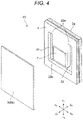
- FIG. 4 is an exploded perspective view of the first bonding portion 20 indicated by an arrow IV in the front view of FIG. 1A .
- the free end 32 b of the support piece 32 faces the left lateral direction (the X 1 direction) in the second bonding portion 30 provided in the left extension 5 b
- the free end 32 b of the support piece 32 faces the right lateral direction (the X 2 direction) in the second bonding portion 30 provided in the right extension 5 c
- the free ends 32 b of the support pieces 32 face the directions opposite to each other in the lateral direction between the second bonding portion 30 provided on the left extension 5 b and the second bonding portion 30 provided on the right extension 5 c. Therefore, as illustrated in FIG.
Abstract
Description
Claims (14)
Applications Claiming Priority (3)
| Application Number | Priority Date | Filing Date | Title |
|---|---|---|---|
| JP2019-007791 | 2019-01-21 | ||
| JPJP2019-007791 | 2019-01-21 | ||
| JP2019007791A JP7106223B2 (en) | 2019-01-21 | 2019-01-21 | Display device |
Publications (2)
| Publication Number | Publication Date |
|---|---|
| US20200233259A1 US20200233259A1 (en) | 2020-07-23 |
| US11442301B2 true US11442301B2 (en) | 2022-09-13 |
Family
ID=69177070
Family Applications (1)
| Application Number | Title | Priority Date | Filing Date |
|---|---|---|---|
| US16/741,090 Active 2040-08-08 US11442301B2 (en) | 2019-01-21 | 2020-01-13 | Display device |
Country Status (4)
| Country | Link |
|---|---|
| US (1) | US11442301B2 (en) |
| EP (1) | EP3683621B1 (en) |
| JP (1) | JP7106223B2 (en) |
| CN (1) | CN111452732B (en) |
Families Citing this family (2)
| Publication number | Priority date | Publication date | Assignee | Title |
|---|---|---|---|---|
| KR20230036008A (en) * | 2021-09-06 | 2023-03-14 | 현대모비스 주식회사 | Vehicle table device |
| CN116669364B (en) * | 2022-12-16 | 2024-04-12 | 荣耀终端有限公司 | Shell and electronic equipment |
Citations (27)
| Publication number | Priority date | Publication date | Assignee | Title |
|---|---|---|---|---|
| US3743801A (en) * | 1972-03-23 | 1973-07-03 | Avco Corp | Tire deflation pressure switch using a dimpling dome pressure |
| US4688074A (en) * | 1982-04-06 | 1987-08-18 | Citizen Watch Co., Ltd. | Connecting structure for a display device |
| US5801542A (en) * | 1995-04-20 | 1998-09-01 | Enplas Corporation | Display panel inspection socket |
| US20020044329A1 (en) * | 2000-08-10 | 2002-04-18 | Hitoshi Shoji | Electrooptical unit and electronic apparatus |
| US20020047974A1 (en) * | 2000-08-22 | 2002-04-25 | Kimikazu Matsumoto | Active matrix liquid crystal display unit having liquid crystal molecules less arranged like spray pattern and along bent line |
| US20020080297A1 (en) * | 2000-12-27 | 2002-06-27 | Ki-Hyub Sung | Display apparatus |
| US20020126248A1 (en) * | 2001-03-07 | 2002-09-12 | Takamasa Yoshida | Display device |
| US20020171783A1 (en) * | 2001-05-21 | 2002-11-21 | Dong-Wook Yang | Liquid crystal display monitor having simplified assembly process |
| US20030011736A1 (en) * | 2001-07-10 | 2003-01-16 | Jin-Ho Ha | Liquid cystal display device |
| US6577288B1 (en) * | 1998-03-20 | 2003-06-10 | Samsung Electronics Co., Ltd. | Flat panel display device for protecting a liquid crystal display thereof |
| JP2005079865A (en) | 2003-08-29 | 2005-03-24 | Toshiba Corp | Display device |
| US20050062899A1 (en) * | 2003-09-19 | 2005-03-24 | Norihisa Fukayama | Display device |
| US20050190336A1 (en) * | 2004-01-30 | 2005-09-01 | Chi Mei Optoelectronics Corp. | Liquid crystal display device |
| US20050212991A1 (en) * | 2004-03-25 | 2005-09-29 | Nec Lcd Technologies, Ltd. | Liquid crystal display module and back light for the same |
| US20070218732A1 (en) * | 2004-05-20 | 2007-09-20 | Kazuki Honda | Portable electronic device |
| US20080310094A1 (en) * | 2007-03-19 | 2008-12-18 | James Allen Burns | Attachable device accessory case cover with interchangeable components |
| US20090185104A1 (en) * | 2008-01-21 | 2009-07-23 | Orion Electric Co., Ltd. | Liquid crystal display panel |
| US20100073582A1 (en) * | 2008-09-19 | 2010-03-25 | Hitachi Consumer Electronics, Co., Ltd. | Liquid crystal display device and video display device using the same |
| US20110049000A1 (en) * | 2009-08-28 | 2011-03-03 | Victor Company Of Japan, Ltd. | Package structure for thin display apparatus and method of packing thin display apparatus |
| WO2013187281A1 (en) | 2012-06-11 | 2013-12-19 | シャープ株式会社 | Display device |
| US20140232969A1 (en) | 2013-02-20 | 2014-08-21 | Japan Display Inc. | Liquid crystal display device, electronic apparatus, and method of fixing display cover |
| US20150055053A1 (en) * | 2013-08-20 | 2015-02-26 | Funai Electric Co., Ltd. | Display device and support member thereof |
| US20150212363A1 (en) * | 2014-01-27 | 2015-07-30 | Canon Kabushiki Kaisha | Display device |
| US20160183399A1 (en) | 2014-12-23 | 2016-06-23 | Samsung Display Co., Ltd. | Display device including curved display panel |
| US20160195770A1 (en) * | 2013-08-23 | 2016-07-07 | Sakai Display Products Corporation | Light source device and display apparatus |
| JP2016122151A (en) | 2014-12-25 | 2016-07-07 | アルパイン株式会社 | Display device |
| US11026336B1 (en) * | 2019-12-03 | 2021-06-01 | Shanghai Tianma AM-OLED Co., Ltd. | Display device |
Family Cites Families (4)
| Publication number | Priority date | Publication date | Assignee | Title |
|---|---|---|---|---|
| TWI282884B (en) * | 2004-02-19 | 2007-06-21 | Hannstar Display Corp | Display module |
| JP3908241B2 (en) * | 2004-06-24 | 2007-04-25 | オリンパス株式会社 | Video display device |
| JP2014202830A (en) * | 2013-04-02 | 2014-10-27 | 船井電機株式会社 | Display device |
| DE102014111676A1 (en) * | 2014-08-15 | 2016-02-18 | Visteon Global Technologies, Inc. | Device for mounting a display element in a motor vehicle |
-
2019
- 2019-01-21 JP JP2019007791A patent/JP7106223B2/en active Active
-
2020
- 2020-01-13 US US16/741,090 patent/US11442301B2/en active Active
- 2020-01-14 CN CN202010034618.5A patent/CN111452732B/en active Active
- 2020-01-17 EP EP20152419.6A patent/EP3683621B1/en active Active
Patent Citations (28)
| Publication number | Priority date | Publication date | Assignee | Title |
|---|---|---|---|---|
| US3743801A (en) * | 1972-03-23 | 1973-07-03 | Avco Corp | Tire deflation pressure switch using a dimpling dome pressure |
| US4688074A (en) * | 1982-04-06 | 1987-08-18 | Citizen Watch Co., Ltd. | Connecting structure for a display device |
| US5801542A (en) * | 1995-04-20 | 1998-09-01 | Enplas Corporation | Display panel inspection socket |
| US6577288B1 (en) * | 1998-03-20 | 2003-06-10 | Samsung Electronics Co., Ltd. | Flat panel display device for protecting a liquid crystal display thereof |
| US20020044329A1 (en) * | 2000-08-10 | 2002-04-18 | Hitoshi Shoji | Electrooptical unit and electronic apparatus |
| US20020047974A1 (en) * | 2000-08-22 | 2002-04-25 | Kimikazu Matsumoto | Active matrix liquid crystal display unit having liquid crystal molecules less arranged like spray pattern and along bent line |
| US20020080297A1 (en) * | 2000-12-27 | 2002-06-27 | Ki-Hyub Sung | Display apparatus |
| US20020126248A1 (en) * | 2001-03-07 | 2002-09-12 | Takamasa Yoshida | Display device |
| US20020171783A1 (en) * | 2001-05-21 | 2002-11-21 | Dong-Wook Yang | Liquid crystal display monitor having simplified assembly process |
| US20030011736A1 (en) * | 2001-07-10 | 2003-01-16 | Jin-Ho Ha | Liquid cystal display device |
| JP2005079865A (en) | 2003-08-29 | 2005-03-24 | Toshiba Corp | Display device |
| US20050062899A1 (en) * | 2003-09-19 | 2005-03-24 | Norihisa Fukayama | Display device |
| US20050190336A1 (en) * | 2004-01-30 | 2005-09-01 | Chi Mei Optoelectronics Corp. | Liquid crystal display device |
| US20050212991A1 (en) * | 2004-03-25 | 2005-09-29 | Nec Lcd Technologies, Ltd. | Liquid crystal display module and back light for the same |
| US20070218732A1 (en) * | 2004-05-20 | 2007-09-20 | Kazuki Honda | Portable electronic device |
| US20080310094A1 (en) * | 2007-03-19 | 2008-12-18 | James Allen Burns | Attachable device accessory case cover with interchangeable components |
| US20090185104A1 (en) * | 2008-01-21 | 2009-07-23 | Orion Electric Co., Ltd. | Liquid crystal display panel |
| US20100073582A1 (en) * | 2008-09-19 | 2010-03-25 | Hitachi Consumer Electronics, Co., Ltd. | Liquid crystal display device and video display device using the same |
| US20110049000A1 (en) * | 2009-08-28 | 2011-03-03 | Victor Company Of Japan, Ltd. | Package structure for thin display apparatus and method of packing thin display apparatus |
| US20150168767A1 (en) | 2012-06-11 | 2015-06-18 | Sharp Kabushiki Kaisha | Display device |
| WO2013187281A1 (en) | 2012-06-11 | 2013-12-19 | シャープ株式会社 | Display device |
| US20140232969A1 (en) | 2013-02-20 | 2014-08-21 | Japan Display Inc. | Liquid crystal display device, electronic apparatus, and method of fixing display cover |
| US20150055053A1 (en) * | 2013-08-20 | 2015-02-26 | Funai Electric Co., Ltd. | Display device and support member thereof |
| US20160195770A1 (en) * | 2013-08-23 | 2016-07-07 | Sakai Display Products Corporation | Light source device and display apparatus |
| US20150212363A1 (en) * | 2014-01-27 | 2015-07-30 | Canon Kabushiki Kaisha | Display device |
| US20160183399A1 (en) | 2014-12-23 | 2016-06-23 | Samsung Display Co., Ltd. | Display device including curved display panel |
| JP2016122151A (en) | 2014-12-25 | 2016-07-07 | アルパイン株式会社 | Display device |
| US11026336B1 (en) * | 2019-12-03 | 2021-06-01 | Shanghai Tianma AM-OLED Co., Ltd. | Display device |
Non-Patent Citations (2)
| Title |
|---|
| Extended European Search Report for 20152419.6 dated Apr. 1, 2020, 6 pgs. |
| Notification of Reasons for Refusal from corresponding Japanese Application No. 2019-007791, dated Feb. 22, 2022, 5pp (including English translation). |
Also Published As
| Publication number | Publication date |
|---|---|
| US20200233259A1 (en) | 2020-07-23 |
| JP2020118759A (en) | 2020-08-06 |
| CN111452732A (en) | 2020-07-28 |
| EP3683621A1 (en) | 2020-07-22 |
| CN111452732B (en) | 2024-03-01 |
| JP7106223B2 (en) | 2022-07-26 |
| EP3683621B1 (en) | 2022-11-02 |
Similar Documents
| Publication | Publication Date | Title |
|---|---|---|
| JP6399926B2 (en) | Display device | |
| US10598974B2 (en) | On-vehicle display device | |
| US11442301B2 (en) | Display device | |
| KR102237372B1 (en) | Connection Holder and Display Device having the same | |
| US11904689B2 (en) | Display device for vehicle | |
| US10583789B2 (en) | Fixing device for panel member | |
| US20190155090A1 (en) | Liquid crystal display device | |
| US11112633B2 (en) | Display apparatus and method for assembling the same | |
| JP6988857B2 (en) | Display device for vehicles | |
| JP2013235185A (en) | Display device | |
| US20200132924A1 (en) | Lighting device and display device | |
| KR20210073467A (en) | Display device | |
| CN111856801B (en) | Display device and method for assembling the same | |
| US20220314795A1 (en) | In-vehicle display device | |
| JPWO2019208425A1 (en) | Liquid crystal display device | |
| US20230314856A1 (en) | Display device | |
| JP2021131454A (en) | Display device | |
| JP2023165435A (en) | display device | |
| JP2021047243A (en) | Display device | |
| CN116097159A (en) | Lighting unit with centering device for optical conductor |
Legal Events
| Date | Code | Title | Description |
|---|---|---|---|
| AS | Assignment |
Owner name: ALPINE ELECTRONICS, INC., JAPAN Free format text: ASSIGNMENT OF ASSIGNORS INTEREST;ASSIGNORS:YAMAZAKI, MAKOTO;AKAMURA, TAKAHIRO;REEL/FRAME:051498/0004 Effective date: 20200106 |
|
| FEPP | Fee payment procedure |
Free format text: ENTITY STATUS SET TO UNDISCOUNTED (ORIGINAL EVENT CODE: BIG.); ENTITY STATUS OF PATENT OWNER: LARGE ENTITY |
|
| STPP | Information on status: patent application and granting procedure in general |
Free format text: APPLICATION DISPATCHED FROM PREEXAM, NOT YET DOCKETED |
|
| STPP | Information on status: patent application and granting procedure in general |
Free format text: DOCKETED NEW CASE - READY FOR EXAMINATION |
|
| STPP | Information on status: patent application and granting procedure in general |
Free format text: NON FINAL ACTION MAILED |
|
| STPP | Information on status: patent application and granting procedure in general |
Free format text: FINAL REJECTION MAILED |
|
| STPP | Information on status: patent application and granting procedure in general |
Free format text: DOCKETED NEW CASE - READY FOR EXAMINATION |
|
| STPP | Information on status: patent application and granting procedure in general |
Free format text: NOTICE OF ALLOWANCE MAILED -- APPLICATION RECEIVED IN OFFICE OF PUBLICATIONS |
|
| STPP | Information on status: patent application and granting procedure in general |
Free format text: PUBLICATIONS -- ISSUE FEE PAYMENT VERIFIED |
|
| STCF | Information on status: patent grant |
Free format text: PATENTED CASE |