US11437189B2 - Electronic component having plurality of internal electrodes - Google Patents
Electronic component having plurality of internal electrodes Download PDFInfo
- Publication number
- US11437189B2 US11437189B2 US17/160,531 US202117160531A US11437189B2 US 11437189 B2 US11437189 B2 US 11437189B2 US 202117160531 A US202117160531 A US 202117160531A US 11437189 B2 US11437189 B2 US 11437189B2
- Authority
- US
- United States
- Prior art keywords
- electrode
- internal electrodes
- portions
- edge line
- end surface
- Prior art date
- Legal status (The legal status is an assumption and is not a legal conclusion. Google has not performed a legal analysis and makes no representation as to the accuracy of the status listed.)
- Active
Links
Images


Classifications
-
- H—ELECTRICITY
- H01—ELECTRIC ELEMENTS
- H01G—CAPACITORS; CAPACITORS, RECTIFIERS, DETECTORS, SWITCHING DEVICES, LIGHT-SENSITIVE OR TEMPERATURE-SENSITIVE DEVICES OF THE ELECTROLYTIC TYPE
- H01G4/00—Fixed capacitors; Processes of their manufacture
- H01G4/30—Stacked capacitors
-
- H—ELECTRICITY
- H01—ELECTRIC ELEMENTS
- H01G—CAPACITORS; CAPACITORS, RECTIFIERS, DETECTORS, SWITCHING DEVICES, LIGHT-SENSITIVE OR TEMPERATURE-SENSITIVE DEVICES OF THE ELECTROLYTIC TYPE
- H01G4/00—Fixed capacitors; Processes of their manufacture
- H01G4/002—Details
- H01G4/005—Electrodes
- H01G4/012—Form of non-self-supporting electrodes
-
- H—ELECTRICITY
- H01—ELECTRIC ELEMENTS
- H01G—CAPACITORS; CAPACITORS, RECTIFIERS, DETECTORS, SWITCHING DEVICES, LIGHT-SENSITIVE OR TEMPERATURE-SENSITIVE DEVICES OF THE ELECTROLYTIC TYPE
- H01G4/00—Fixed capacitors; Processes of their manufacture
- H01G4/002—Details
- H01G4/005—Electrodes
-
- H—ELECTRICITY
- H01—ELECTRIC ELEMENTS
- H01G—CAPACITORS; CAPACITORS, RECTIFIERS, DETECTORS, SWITCHING DEVICES, LIGHT-SENSITIVE OR TEMPERATURE-SENSITIVE DEVICES OF THE ELECTROLYTIC TYPE
- H01G4/00—Fixed capacitors; Processes of their manufacture
- H01G4/002—Details
- H01G4/005—Electrodes
- H01G4/008—Selection of materials
-
- H—ELECTRICITY
- H01—ELECTRIC ELEMENTS
- H01G—CAPACITORS; CAPACITORS, RECTIFIERS, DETECTORS, SWITCHING DEVICES, LIGHT-SENSITIVE OR TEMPERATURE-SENSITIVE DEVICES OF THE ELECTROLYTIC TYPE
- H01G4/00—Fixed capacitors; Processes of their manufacture
- H01G4/002—Details
- H01G4/228—Terminals
- H01G4/232—Terminals electrically connecting two or more layers of a stacked or rolled capacitor
-
- H—ELECTRICITY
- H01—ELECTRIC ELEMENTS
- H01G—CAPACITORS; CAPACITORS, RECTIFIERS, DETECTORS, SWITCHING DEVICES, LIGHT-SENSITIVE OR TEMPERATURE-SENSITIVE DEVICES OF THE ELECTROLYTIC TYPE
- H01G4/00—Fixed capacitors; Processes of their manufacture
- H01G4/002—Details
- H01G4/005—Electrodes
- H01G4/008—Selection of materials
- H01G4/0085—Fried electrodes
-
- H—ELECTRICITY
- H01—ELECTRIC ELEMENTS
- H01G—CAPACITORS; CAPACITORS, RECTIFIERS, DETECTORS, SWITCHING DEVICES, LIGHT-SENSITIVE OR TEMPERATURE-SENSITIVE DEVICES OF THE ELECTROLYTIC TYPE
- H01G4/00—Fixed capacitors; Processes of their manufacture
- H01G4/002—Details
- H01G4/018—Dielectrics
- H01G4/06—Solid dielectrics
- H01G4/08—Inorganic dielectrics
- H01G4/12—Ceramic dielectrics
- H01G4/1209—Ceramic dielectrics characterised by the ceramic dielectric material
- H01G4/1218—Ceramic dielectrics characterised by the ceramic dielectric material based on titanium oxides or titanates
-
- H—ELECTRICITY
- H01—ELECTRIC ELEMENTS
- H01G—CAPACITORS; CAPACITORS, RECTIFIERS, DETECTORS, SWITCHING DEVICES, LIGHT-SENSITIVE OR TEMPERATURE-SENSITIVE DEVICES OF THE ELECTROLYTIC TYPE
- H01G4/00—Fixed capacitors; Processes of their manufacture
- H01G4/002—Details
- H01G4/224—Housing; Encapsulation
Definitions
- the present invention relates to an electronic component.
- An electronic component including an element body including a side surface and an end surface adjacent to each other, an external electrode disposed on the side surface and the end surface, and an internal electrode disposed in the element body is known (for example, see Japanese Unexamined Patent Publication No. 2003-22930).
- the element body has a rectangular parallelepiped shape in which a corner portion and an edge line portion are rounded.
- the internal electrode has a rectangular shape and is exposed to the end surface of the element body to be connected to the external electrode.
- chipping there is a likelihood that chipping (chipping) will occur in an element body, for example, during the manufacturing process.
- chipping chipping
- an impact is applied to the element body. Since a corner portion of the element body has a relatively low strength, there is a high likelihood that chipping will occur on the corner portion when an impact is applied. Therefore, occurrence of chipping in the element body is suppressed by forming a corner portion and an edge line portion of the element body into a curved surface shape.
- An external electrode generally includes an electrode layer disposed on a side surface and an end surface, and a plated layer disposed to cover the electrode layer.
- the plated layer is formed on the electrode layer using a plating method.
- the plating solution may enter an interface between the external electrode and the element body through the external electrode due to a pressure difference between the outside and inside of the external electrode (electrode layer).
- An end portion of an internal electrode is exposed to a surface of the element body to be connected to the external electrode. Therefore, the plating solution that has entered the interface between the external electrode and the element body may enter the inside of the element body through an interface between the end portion or an internal conductor of the internal electrode and the element body.
- the corner portion and the edge line portion of the element body have a curved surface shape
- thicknesses of the external electrode at the corner portion and the edge line portion decrease, and this causes the plating solution to easily enter. Entering of the plating solution into the element body causes decrease in reliability of the electronic component. Also, increase in capacitance is desired in electronic components.
- An objective of one aspect of the present invention is to provide an electronic component in which increase in capacitance can be achieved while achieving improvement in reliability.
- An electronic component includes an element body having a pair of end surfaces facing each other and four side surfaces connecting the pair of end surfaces, an external electrode disposed on the side surfaces and each of the end surfaces, and a plurality of internal electrodes disposed in the element body, in which the element body has a first edge line surface which is provided between the end surface and each of the side surfaces and which is curved, and a second edge line surface which is provided between two adjacent side surfaces and which is curved, the external electrode has an electrode layer provided across the end surface and a part of the side surface and a plated layer covering the electrode layer, the plurality of internal electrodes each have an electrode portion disposed to face other internal electrodes and a connecting portion connecting the electrode portion and the external electrode, the connecting portions of the internal electrodes are positioned in a region corresponding to the end surface when viewed from a direction perpendicular to the end surface, and the electrode portions of the internal electrodes have portions overlapping a region corresponding to the first edge line surface when viewed from the direction perpendicular to the end surface, and
- the connecting portions of the internal electrodes are positioned in the region corresponding to the end surface when viewed from a direction perpendicular to the end surface. That is, the connecting portions of the internal electrodes are not positioned in the region corresponding to the first edge line surface when viewed from the direction perpendicular to the end surface.
- the electrode portions of the internal electrodes have portions overlapping the region of the first edge line surface when viewed from the direction perpendicular to the end surface. Therefore, areas of the electrode portions can be increased in the electronic component. Therefore, increase in capacitance can be achieved in the electronic component.
- a radius of curvature of a corner portion of the element body may be larger than a radius of curvature of the second edge line surface. In this configuration, occurrence of chipping in the element body can be further suppressed.
- all the connecting portions of the plurality of internal electrodes may be positioned in the region corresponding to the end surface when viewed from the direction perpendicular to the end surface. In this configuration, all the connecting portions are not positioned in the region corresponding to the first edge line surface when viewed from the direction perpendicular to the end surface. Therefore, in the electronic component, entering of the plating solution into the element body via the connecting portions of the internal electrodes can be further suppressed in the plating process of forming the plated layer of the external electrode.
- the electrode portions of two internal electrodes disposed at end portions in a lamination direction of the plurality of internal electrodes may have portions overlapping the region corresponding to the first edge line surface at positions facing each other in the lamination direction. In this configuration, since the areas of the electrode portions of the internal electrodes can be increased, the capacitance can be increased.
- all the electrode portions of the plurality of internal electrodes may have portions overlapping the region corresponding to the first edge line surface when viewed from the direction perpendicular to the end surface. In this configuration, since the areas of all the electrode portions of the internal electrodes can be increased, the capacitance can be further increased.
- a width of the connecting portion may be smaller than a width of the electrode portion. In this configuration, the capacitance can be increased while suppressing entering of the plating solution.
- both end portions in a direction in which a pair of side surfaces parallel to the lamination direction face each other in the electrode portions of the two internal electrodes disposed at the end portions in the lamination direction of the plurality of internal electrodes may have portions overlapping the region corresponding to the first edge line surface when viewed from the direction perpendicular to the end surface.
- central portions in the direction in which the pair of side surfaces parallel to the lamination direction face each other in the electrode portions of the two internal electrodes disposed at the end portions in the lamination direction of the plurality of internal electrodes may be positioned in the region corresponding to the end surface when viewed from the direction perpendicular to the end surface. In this configuration, the capacitance can be increased while suppressing entering of the plating solution.
- FIG. 1 is a perspective view of a multilayer capacitor according to the present embodiment.
- FIG. 2 is a view illustrating a cross-sectional configuration of the multilayer capacitor according to the present embodiment.
- FIG. 3 is a view illustrating a cross-sectional configuration of the multilayer capacitor according to the present embodiment.
- FIG. 4 is an exploded perspective view of an element body of the multilayer capacitor.
- FIG. 5 is a view illustrating a configuration of an internal electrode.
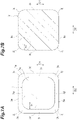
- FIG. 6A is a view illustrating the element body.
- FIG. 6B is a view illustrating a cross-sectional configuration of the element body.
- FIG. 7A is a view illustrating the element body.
- FIG. 7B is a view illustrating a cross-sectional configuration of the element body.
- a multilayer capacitor (electronic component) 1 includes an element body 3 having a rectangular parallelepiped shape and a plurality of external electrodes 5 .
- the multilayer capacitor 1 includes a pair of external electrodes 5 .
- the pair of external electrodes 5 are disposed on an outer surface of the element body 3 .
- the pair of external electrodes 5 are spaced apart from each other.
- the rectangular parallelepiped shape includes a rectangular parallelepiped shape in which corner portions and edge line portions are chamfered, and a rectangular parallelepiped shape in which corner portions and edge line portions are rounded.
- the element body 3 includes a pair of main surfaces 3 a facing each other, a pair of side surfaces 3 c facing each other, and a pair of end surfaces 3 e facing each other.
- the pair of main surfaces 3 a , the pair of side surfaces 3 c , and the pair of end surfaces 3 e have a rectangular shape.
- the rectangular shape may include, for example, a shape in which each corner is curved, that is, a shape in which each corner is chamfered, and a shape in which each corner is rounded.
- a direction in which the pair of main surfaces 3 a face each other is a first direction D 1 .
- a direction in which the pair of side surfaces 3 c face each other is a second direction D 2 .
- a direction in which the pair of end surfaces 3 e face each other is a third direction D 3 .
- the multilayer capacitor 1 is solder-mounted on an electronic device.
- the electronic device may include, for example, circuit boards or electronic components.
- one main surface 3 a faces the electronic device.
- One main surface 3 a is disposed to form a mounting surface.
- One main surface 3 a is a mounting surface.
- Each of the main surfaces 3 a is also a side surface of the element body 3 having a rectangular parallelepiped shape.
- the first direction D 1 is a direction perpendicular to the main surfaces 3 a and is perpendicular to the second direction D 2 .
- the third direction D 3 is a direction parallel to the main surfaces 3 a and the side surfaces 3 c and is perpendicular to the first direction D 1 and the second direction D 2 .
- the second direction D 2 is a direction perpendicular to the side surfaces 3 c
- the third direction D 3 is a direction perpendicular to the end surfaces 3 e .
- a length of the element body 3 in the first direction D 1 is larger than a length of the element body 3 in the second direction D 2 .
- a length of the element body 3 in the third direction D 3 is larger than the length of the element body 3 in the first direction D 1 and larger than the length of the element body 3 in the second direction D 2 .
- the third direction D 3 is a longitudinal direction of the element body 3 .
- the length of the element body 3 in the first direction D 1 is a height of the element body 3 .
- the length of the element body 3 in the second direction D 2 is a width of the element body 3 .
- the length of the element body 3 in the third direction D 3 is a length of the element body 3 .
- the height of the element body 3 may be 1880 ⁇ m
- the width of the element body 3 may be 1840 ⁇ m
- the length of the element body 3 may be 3330 ⁇ m.
- the multilayer capacitor 1 is a so-called C3216 type product.
- the pair of side surfaces 3 c extend in the first direction D 1 to connect the pair of main surfaces 3 a .
- the pair of side surfaces 3 c also extend in the third direction D 3 .
- the pair of end surfaces 3 e extend in the first direction D 1 to connect the pair of main surfaces 3 a .
- the pair of end surfaces 3 e also extend in the second direction D 2 .
- the element body 3 includes four edge line surfaces (first edge line surface) 3 g , four edge line surfaces (first edge line surface) 3 i , and four edge line surfaces (second edge line surface) 3 j .
- the edge line surfaces 3 g are each positioned between the end surface 3 e and the main surface 3 a .
- the edge line surfaces 3 i are each positioned between the end surface 3 e and the side surface 3 c .
- the edge line surfaces 3 j are each positioned between the main surface 3 a and the side surface 3 c .
- the edge line surfaces 3 g , 3 i , and 3 j are each rounded to be curved in a convex shape.
- the edge line surfaces 3 g , 3 i , and 3 j are each a curved surface having a predetermined radius of curvature.
- the element body 3 has been subjected to so-called R chamfering.
- the end surface 3 e and the main surface 3 a are indirectly adjacent to each other via the edge line surface 3 g .
- the end surface 3 e and the side surface 3 c are indirectly adjacent to each other via the edge line surface 3 i .
- the main surface 3 a and the side surface 3 c are indirectly adjacent to each other via the edge line surface 3 j.
- the element body 3 includes corner portions 3 k .
- the corner portions 3 k are each rounded to be curved. That is, each corner portion 3 k has a curved surface shape.
- the corner portion 3 k is an intersecting portion of the edge line surface 3 g and the edge line surface 3 i . That is, the edge line surface 3 g and the edge line surface 3 i form the corner portion 3 k.
- the element body 3 is configured to have a plurality of dielectric layers 6 laminated in the first direction D 1 .
- the element body 3 includes the plurality of laminated dielectric layers 6 .
- a lamination direction of the plurality of dielectric layers 6 coincides with the first direction D 1 .
- Each of the dielectric layers 6 may be formed of, for example, a sintered body of a ceramic green sheet containing a dielectric material.
- the dielectric material may include, for example, a BaTiO 3 -based dielectric ceramic, a Ba(Ti, Zr)O 3 -based dielectric ceramic, a (Ba, Ca)TiO 3 -based dielectric ceramic, or the like.
- the dielectric layers 6 are integrated to such an extent that boundaries between the respective dielectric layers 6 cannot be visually recognized.
- the multilayer capacitor 1 includes a plurality of internal electrodes 7 and a plurality of internal electrodes 9 .
- the multilayer capacitor 1 includes four internal electrodes 7 and four internal electrodes 9 .
- Each of the internal electrodes 7 and 9 is an internal conductor disposed in the element body 3 .
- Each of the internal electrodes 7 and 9 is made of a conductive material normally used for internal electrodes of lamination-type electronic components.
- the conductive material may include, for example, a base metal.
- the conductive material may include, for example, Ni or Cu.
- the internal electrodes 7 and 9 are formed as a sintered body of a conductive paste containing the above-described conductive material.
- the internal electrodes 7 and the internal electrodes 9 are disposed at different positions (layers) in the first direction D 1 .
- the internal electrodes 7 and the internal electrodes 9 are alternately disposed to face each other with a distance therebetween in the first direction D 1 .
- the internal electrode 7 and the internal electrode 9 have different polarities from each other.
- the plurality of internal electrodes 7 and the plurality of internal electrodes 9 are alternately aligned in the first direction D 1 .
- the internal electrodes 7 and 9 are each positioned in a plane that is substantially parallel to the main surfaces 3 a .
- the internal electrodes 7 and the internal electrodes 9 face each other in the first direction D 1 .
- a direction in which the internal electrodes 7 and the internal electrodes 9 face each other (the first direction D 1 ) is perpendicular to a direction parallel to the main surfaces 3 a (the second direction D 2 and the third direction D 3 ).
- a distance between the internal electrode 7 closest to one main surface 3 a and the internal electrode 9 closest to the other main surface 3 a may be, for example, 1500 ⁇ m.
- the internal electrodes 7 each include an electrode portion 7 a and a connecting portion 7 b .
- the electrode portion 7 a has a rectangular shape.
- the connecting portion 7 b has a rectangular shape.
- the connecting portion 7 b extends from one side of the electrode portion 7 a and is exposed to corresponding one end surface 3 e .
- the connecting portion 7 b extends from one side of the electrode portion 7 a on one end surface 3 e side so that a central portion of the connecting portion 7 b in the second direction D 2 and a central portion of the electrode portion 7 a in the second direction D 2 are substantially coincident with each other.
- the connecting portion 7 b of the internal electrode 7 exposed to one end surface 3 e is joined to the external electrode 5 .
- the connecting portion 7 b connects the electrode portion 7 a and the external electrode 5 . Thereby, the internal electrode 7 is electrically connected to the external electrode 5 .
- a width W 1 of the electrode portion 7 a in the second direction D 2 is larger than a width W 2 of the connecting portion 7 b .
- the width W 2 of the connecting portion 7 b is smaller than the width W 1 of the electrode portion 7 a .
- the width W 1 of the electrode portion 7 a may be 1500 ⁇ m
- the width W 2 of the connecting portion 7 b may be 750 ⁇ m. That is, the width W 1 of the electrode portion 7 a is twice the width W 2 of the connecting portion 7 b .
- a length of the electrode portion 7 a in the third direction D 3 may be 2990 ⁇ m
- a length of the connecting portion 7 b in the third direction D 3 may be 170 ⁇ m.
- the internal electrode 9 includes an electrode portion 9 a and a connecting portion 9 b .
- the electrode portion 9 a has a rectangular shape.
- the connecting portion 9 b has a rectangular shape.
- the connecting portion 9 b extends from one side of the electrode portion 9 a and is exposed to the corresponding other end surface 3 e .
- the connecting portion 9 b extends from one side of the electrode portion 9 a on the other end surface 3 e side so that a central portion of the connecting portion 9 b in the second direction D 2 and a central portion of the electrode portion 9 a in the second direction D 2 are substantially coincident with each other.
- the connecting portion 9 b of the internal electrode 9 exposed to the other end surface 3 e is joined to the external electrode 5 .
- the connecting portion 9 b connects the electrode portion 9 a and the external electrode 5 . Thereby, the internal electrode 9 is electrically connected to the external electrode 5 .
- a width W 1 of the electrode portion 9 a in the second direction D 2 is larger than a width W 2 of the connecting portion 9 b .
- the width W 2 of the connecting portion 9 b is smaller than the width W 1 of the electrode portion 9 a .
- the width W 1 of the electrode portion 9 a may be 1500 ⁇ m
- the width W 2 of the connecting portion 9 b may be 750 ⁇ m. That is, the width W 1 of the electrode portion 9 a is twice the width W 2 of the connecting portion 9 b .
- a length of the electrode portion 9 a in the third direction D 3 may be 2990 ⁇ m
- a length of the connecting portion 9 b in the third direction D 3 may be 170 ⁇ m.
- the external electrodes 5 are disposed at both end portions of the element body 3 in the third direction D 3 .
- the external electrodes 5 are respectively disposed on corresponding end surface 3 e sides of the element body 3 .
- the external electrodes 5 are each disposed on the pair of main surfaces 3 a , the pair of side surfaces 3 c , and one end surface 3 e .
- the external electrode 5 includes a plurality of electrode portions 5 a , 5 c , and 5 e as illustrated in FIGS. 2 and 3 .
- the electrode portion 5 a is disposed on the main surface 3 a and the edge line surface 3 g .
- the electrode portion 5 c is disposed on the side surface 3 c and the edge line surface 3 i .
- the electrode portion 5 e is disposed on the end surface 3 e .
- the external electrode 5 also includes an electrode portion disposed on the edge line surface 3 j.
- the external electrode 5 is formed on five surfaces of the pair of main surfaces 3 a , one end surface 3 e , and the pair of side surfaces 3 c , and on the edge line surfaces 3 g , 3 i , and 3 j .
- the electrode portions 5 a , 5 c , and 5 e adjacent to each other are connected and electrically connected.
- the electrode portion 5 e covers all of one ends of corresponding internal electrodes 7 and 9 .
- the electrode portion 5 e is directly connected to the corresponding internal electrodes 7 and 9 .
- the external electrode 5 is electrically connected to the corresponding internal electrodes 7 and 9 .
- the external electrode 5 includes a first electrode layer E 1 , a second electrode layer E 2 , and a third electrode layer E 3 .
- the third electrode layer E 3 constitutes an outermost layer of the external electrode 5 .
- the electrode portions 5 a , 5 c , and 5 e each have the first electrode layer E 1 , the second electrode layer E 2 , and
- the first electrode layer E 1 is disposed on a part of the main surface 3 a , a part of the side surface 3 c , and the end surface 3 e .
- a part of the main surface 3 a and a part of the side surface 3 c may be, for example, parts of the main surface 3 a and the side surface 3 c that are close to the end surface 3 e .
- the first electrode layer E 1 is formed to cover the edge line surfaces 3 g , 3 i , and 3 j .
- the first electrode layer E 1 is formed to cover the entire edge line surface 3 g and edge line surface 3 i .
- the first electrode layer E 1 is in contact with the entire edge line surface 3 g and edge line surface 3 i.
- the first electrode layer E 1 is formed by baking a conductive paste applied to a surface of the element body 3 .
- the first electrode layer E 1 is formed when a metal component (metal powder) contained in the conductive paste is sintered.
- the first electrode layer E 1 is a sintered metal layer (electrode layer).
- the first electrode layer E 1 is a sintered metal layer formed on the element body 3 .
- the first electrode layer E 1 is a sintered metal layer made of Cu.
- the first electrode layer E 1 may also be a sintered metal layer made of Ni.
- the first electrode layer E 1 contains a base metal.
- the conductive paste may contain, for example, a powder made of Cu or Ni, a glass component, an organic binder, and an organic solvent.
- Each first electrode layer E 1 included in the electrode portions 5 a , 5 c , and 5 e are integrally formed.
- the second electrode layer E 2 is disposed on the first electrode layer E 1 .
- the second electrode layer E 2 covers the entire first electrode layer E 1 .
- the second electrode layer E 2 is in contact with the entire first electrode layer E 1 .
- the second electrode layer E 2 is in contact with a part of the main surface 3 a and a part of the side surface 3 c .
- the second electrode layer E 2 is formed on the first electrode layer E 1 using a plating method.
- the second electrode layer E 2 is formed on the first electrode layer E 1 by Ni plating.
- the second electrode layer E 2 is a Ni-plated layer.
- the second electrode layer E 2 may also be a Sn-plated layer, a Cu-plated layer, or an Au-plated layer.
- the second electrode layer E 2 contains Ni, Sn, Cu, or Au.
- the Ni-plated layer is superior in solder corrosion resistance to the metal contained in the first electrode layer E 1 .
- the third electrode layer E 3 is disposed on the second electrode layer E 2 .
- the third electrode layer E 3 covers the entire second electrode layer E 2 .
- the third electrode layer E 3 is in contact with the entire second electrode layer E 2 .
- the third electrode layer E 3 is in contact with a part of the main surface 3 a and a part of the side surface 3 c .
- the third electrode layer E 3 is formed on the second electrode layer E 2 using a plating method.
- the third electrode layer E 3 is a solder-plated layer.
- the third electrode layer E 3 is formed on the second electrode layer E 2 by Sn plating.
- the third electrode layer E 3 is a Sn-plated layer.
- the third electrode layer E 3 may also be a Sn—Ag alloy plated layer, a Sn—Bi alloy plated layer, or a Sn—Cu alloy plated layer.
- the third electrode layer E 3 contains Sn, a Sn—Ag alloy, a Sn—Bi alloy, or a Sn—Cu alloy.
- the second electrode layer E 2 and the third electrode layer E 3 form a plated layer PL.
- the plated layer PL has a two-layer structure.
- the plated layer PL covers the first electrode layer E 1 .
- Each second electrode layer E 2 included in the electrode portions 5 a , 5 c , and 5 e are integrally formed.
- Each third electrode layer E 3 included in the electrode portions 5 a , 5 c , and 5 e are integrally formed.
- the connecting portion 7 b of the internal electrode 7 is positioned in a region corresponding to one end surface 3 e when viewed from the direction in which the pair of end surfaces 3 e face each other (the third direction D 3 ).
- all the connecting portions 7 b of the internal electrodes 7 are positioned in the region corresponding to one end surface 3 e when viewed from the third direction D 3 .
- the connecting portions 7 b are exposed only to the end surface 3 e .
- the region corresponding to the end surface 3 e is a region surrounded by the edge line surface 3 g and the edge line surface 3 i .
- the region corresponding to the end surface 3 e has a rectangular shape in which corners thereof are curved.
- the region corresponding to the end surface 3 e is defined by a boundary of the end surface 3 e with the edge line surface 3 g and the edge line surface 3 i (edge of the end surface 3 e ).
- the connecting portions 7 b of the internal electrodes 7 are disposed at positions at which they overlap only the end surface 3 e when viewed from the third direction D 3 .
- the connecting portions 7 b of the internal electrodes 7 are not disposed at positions overlapping the edge line surface 3 g and the edge line surface 3 i when viewed from the third direction D 3 .
- illustration of the external electrode 5 is omitted.
- the connecting portion 9 b of the internal electrode 9 is positioned in a region corresponding to the other end surface 3 e when viewed from the direction in which the pair of end surfaces 3 e face each other (the third direction D 3 ).
- all the connecting portions 9 b of the internal electrodes 9 are positioned in the region corresponding to the other end surface 3 e when viewed from the third direction D 3 .
- the connecting portions 9 b are exposed only to the end surface 3 e .
- the region corresponding to the end surface 3 e is a region surrounded by the edge line surface 3 g and the edge line surface 3 i .
- the region corresponding to the end surface 3 e has a rectangular shape in which corners thereof are curved.
- the region corresponding to the end surface 3 e is defined by a boundary of the end surface 3 e with the edge line surface 3 g and the edge line surface 3 i .
- the connecting portions 9 b of the internal electrodes 9 are disposed at positions at which they overlap only the end surface 3 e when viewed from the third direction D 3 .
- the connecting portions 9 b of the internal electrodes 9 are not disposed at positions overlapping the edge line surface 3 g and the edge line surface 3 i when viewed from the third direction D 3 .
- the electrode portions 7 a and 9 a of two internal electrodes 7 and 9 disposed at end portions in the first direction D 1 have portions overlapping a region corresponding to the edge line surface 3 j and the edge line surface 3 i .
- both end portions in the second direction D 2 of the electrode portion 7 a of the internal electrode 7 that is closest to one main surface 3 a in the first direction D 1 are positioned at regions corresponding to an intersecting portion of the edge line surface 3 j and the edge line surface 3 i when viewed from the third direction D 3 .
- both end portions of the electrode portion 7 a of the internal electrode 7 in the second direction D 2 described above are disposed at positions that do not overlap the region corresponding to the end surface 3 e (a region indicated by a dashed-dotted line) when viewed from the third direction D 3 .
- Both end portions in the second direction D 2 of the electrode portion 7 a of the internal electrode 7 described above protrude in the second direction D 2 from the region corresponding to the end surface 3 e when viewed from the third direction D 3 .
- FIG. 6B illustrates a cross section at a position that is 1 ⁇ 2 of the length of the element body 3 . Therefore, the edge line surface 3 j in FIG. 6B indicates an edge line surface at a position that is 1 ⁇ 2 of the length of the element body 3 .
- Both end portions in the second direction D 2 of the electrode portion 9 a of the internal electrode 9 that is closest to the other main surface 3 a in the first direction D 1 are positioned at regions corresponding to an intersecting portion of the edge line surface 3 j and the edge line surface 3 i when viewed from the third direction D 3 . That is, both end portions in the second direction D 2 of the electrode portion 9 a of the internal electrode 9 described above are disposed at positions that do not overlap the region corresponding to the end surface 3 e when viewed from the third direction D 3 . Both end portions in the second direction D 2 of the electrode portion 9 a of the internal electrode 9 described above protrude in the second direction D 2 from the region corresponding to the end surface 3 e when viewed from the third direction D 3 .
- a central portion in the second direction D 2 of the electrode portion 7 a of the internal electrode 7 that is closest to one main surface 3 a in the first direction D 1 is positioned in the region corresponding to the end surface 3 e when viewed from the third direction D 3 . That is, the central portion of the electrode portion 7 a of the internal electrode 7 in the second direction D 2 described above is disposed at a position that does not overlap the edge line surface 3 j or the edge line surface 3 i when viewed from the third direction D 3 .
- a central portion in the second direction D 2 of the electrode portion 9 a of the internal electrode 9 that is closest to the other main surface 3 a in the first direction D 1 is positioned in the region corresponding to the end surface 3 e when viewed from the third direction D 3 . That is, the central portion of the electrode portion 9 a of the internal electrode 9 in the second direction D 2 described above is disposed at a position that does not overlap the edge line surface 3 j or the edge line surface 3 i when viewed from the third direction D 3
- a radius of curvature R 1 of the corner portion 3 k of the element body 3 is larger than a radius of curvature R 2 of the edge line surface 3 j (R 1 >R 2 ).
- the radius of curvature R 2 of the edge line surface 3 j is smaller than the radius of curvature R 1 of the corner portion 3 k of the element body 3 (R 2 ⁇ R 1 ).
- the radius of curvature R 1 is 140 ⁇ m to 160 ⁇ m.
- the radius of curvature R 1 may be 150 ⁇ m and the radius of curvature R 2 may be 125 ⁇ m.
- illustration of the external electrode 5 is omitted. FIG.
- the edge line surface 3 j in FIG. 7B illustrates an edge line surface at a position that is 1 ⁇ 2 of the length of the element body 3 .
- the radius of curvature R 1 of the corner portion 3 k is 20 ⁇ m to 45 ⁇ m.
- the radius of curvature R 1 of the corner portion 3 k is 60 ⁇ m to 80 ⁇ m.
- the radius of curvature R 1 of the corner portion 3 k is 100 ⁇ m to 120 ⁇ m.
- the radius of curvature R 1 of the corner portion 3 k is 200 ⁇ m to 250 ⁇ m.
- the connecting portions 7 b and 9 b of the internal electrodes 7 and 9 are positioned in the region corresponding to the end surface 3 e when viewed from the direction perpendicular to the end surface 3 e (the third direction D 3 ). That is, the connecting portions 7 b and 9 b of the internal electrodes 7 and 9 are not positioned in the region corresponding to the edge line surface 3 g or the edge line surface 3 i when viewed from the direction perpendicular to the end surface 3 e .
- the electrode portions 7 a and 9 a of the internal electrodes 7 and 9 have portions overlapping a region of the intersecting portion (the corner portion 3 k ) of the edge line surface 3 j and the edge line surface 3 i when viewed from the direction perpendicular to the end surface 3 e .
- areas of the electrode portions 7 a and 9 a can be increased in the multilayer capacitor 1 . Therefore, increase in capacitance can be achieved in the multilayer capacitor 1 .
- the multilayer capacitor 1 includes the edge line surface 3 g and the edge line surface 3 i formed on the element body 3 .
- a thickness of the first electrode layer E 1 formed on the edge line surface 3 g and the edge line surface 3 i can be smaller than a thickness of the first electrode layer E 1 formed on the end surface 3 e . Therefore, in the plating process of forming the plated layer PL of the external electrode 5 , entering of the plating solution is more likely to occur in the first electrode layer E 1 disposed on the edge line surface 3 g and the edge line surface 3 i of the element body 3 than in the first electrode layer E 1 disposed on the end surface 3 e .
- the connecting portions 7 b and 9 b of the internal electrodes 7 and 9 are positioned in the region corresponding to the end surface 3 e when viewed from the direction perpendicular to the end surface 3 e . Therefore, in the multilayer capacitor 1 , entering of the plating solution into the element body 3 via the connecting portions 7 b and 9 b of the internal electrodes 7 and 9 can be suppressed in the plating process of forming the plated layer PL of the external electrode 5 .
- the radius of curvature R 1 of the corner portion 3 k of the element body 3 is larger than the radius of curvature R 2 of the edge line surface 3 j .
- the curvature of the corner portion 3 k is made small in the element body 3 , occurrence of chipping can be further suppressed.
- all the connecting portions 7 b and 9 b of the plurality of internal electrodes 7 and 9 are positioned in the region corresponding to the end surface 3 e when viewed from the direction perpendicular to the end surface 3 e .
- all the connecting portions 7 b and 9 b are not positioned in the region corresponding to the edge line surface 3 g or the edge line surface 3 i when viewed from the direction perpendicular to the end surface 3 e .
- the electrode portions 7 a and 9 a of the two internal electrodes 7 and 9 disposed at the end portions in the lamination direction of the plurality of internal electrodes 7 and 9 have portions overlapping the region of the intersecting portion (the corner portion 3 k ) of the edge line surface 3 j and the edge line surface 3 i at positions facing each other in the lamination direction.
- the capacitance can be increased.
- the width W 2 of the connecting portions 7 b and 9 b of the internal electrodes 7 and 9 is smaller than the width W 1 of the electrode portions 7 a and 9 a . In this configuration, the capacitance can be increased while suppressing entering of the plating solution.
- both end portions in a direction in which the pair of side surfaces 3 c and 3 c parallel to the lamination direction face each other (in the second direction D 2 ) in the electrode portions 7 a and 9 a of the two internal electrodes 7 and 9 disposed at the end portions in the lamination direction of the plurality of internal electrodes 7 and 9 have portions overlapping the region of the intersecting portion (the corner portion 3 k ) of the edge line surface 3 j and the edge line surface 3 i .
- the capacitance can be increased.
- the capacitance when viewed from the direction perpendicular to the end surface 3 e , central portions in the direction in which the pair of side surfaces 3 c and 3 c parallel to the lamination direction face each other (in the second direction D 2 ) in the electrode portions 7 a and 9 a of the two internal electrodes 7 and 9 disposed at the end portions in the lamination direction of the plurality of internal electrodes 7 and 9 are positioned in the region corresponding to the end surface 3 e . In this configuration, the capacitance can be increased while suppressing entering of the plating solution.
- FIG. 6A a configuration in which all the connecting portions 7 b of the internal electrodes 7 are positioned in the end surface 3 e of the element body 3 has been described as an example.
- some of the connecting portions 7 b of the internal electrodes 7 may be positioned in the end surface 3 e of the element body 3 . That is, some of the connecting portions 7 b of the internal electrodes 7 may be positioned at the region corresponding to the edge line surface 3 g and/or the edge line surface 3 i when viewed from the third direction D 3 .
- the width W 1 of the electrode portion 7 a is larger than the width W 2 of the connecting portion 7 b in the internal electrode 7
- the width W 1 of the electrode portion 7 a and the width W 2 of the connecting portion 7 b may be the same as each other in the internal electrode 7 . That is, the internal electrode 7 may have a rectangular shape as a whole. The same applies to the internal electrode 9 .
- the multilayer capacitor 1 includes four internal electrodes 7 and four internal electrodes 9 has been described as an example.
- the number of internal electrodes 7 and 9 may be appropriately set according to a design.
- the electronic component is the multilayer capacitor 1
- the electronic component is not limited to a multilayer capacitor.
- Electronic components to which the present invention can be applied may be, for example, laminated electronic components such as laminated varistors, laminated piezoelectric actuators, laminated thermistors, or laminated composite components, or electronic components other than the laminated electronic components.
- the element when it is described that an element is disposed on another element, the element may be directly disposed on another element or may be indirectly disposed on another element.
- an element When an element is indirectly disposed on another element, there is an intervening element between the element and another element.
- one element is directly disposed on another element, there is no intervening element between the element and another element.
- the element when it is described that an element is positioned on another element, the element may be directly positioned on another element or may be indirectly positioned on another element.
- an element When an element is indirectly positioned on another element, there is an intervening element between the element and another element.
- one element is directly positioned on another element, there is no intervening element between the element and another element.
- an element when it is described that an element covers another element, the element may directly cover another element or may indirectly cover another element. When an element indirectly covers another element, there is an intervening element between the element and another element. When one element directly covers another element, there is no intervening element between the element and another element.
Landscapes
- Engineering & Computer Science (AREA)
- Power Engineering (AREA)
- Manufacturing & Machinery (AREA)
- Microelectronics & Electronic Packaging (AREA)
- Chemical & Material Sciences (AREA)
- Ceramic Engineering (AREA)
- Materials Engineering (AREA)
- Inorganic Chemistry (AREA)
- Ceramic Capacitors (AREA)
- Fixed Capacitors And Capacitor Manufacturing Machines (AREA)
Abstract
Description
Claims (4)
Applications Claiming Priority (3)
| Application Number | Priority Date | Filing Date | Title |
|---|---|---|---|
| JP2020022427A JP7380291B2 (en) | 2020-02-13 | 2020-02-13 | electronic components |
| JP2020-022427 | 2020-02-13 | ||
| JPJP2020-022427 | 2020-02-13 |
Publications (2)
| Publication Number | Publication Date |
|---|---|
| US20210257160A1 US20210257160A1 (en) | 2021-08-19 |
| US11437189B2 true US11437189B2 (en) | 2022-09-06 |
Family
ID=77180913
Family Applications (1)
| Application Number | Title | Priority Date | Filing Date |
|---|---|---|---|
| US17/160,531 Active US11437189B2 (en) | 2020-02-13 | 2021-01-28 | Electronic component having plurality of internal electrodes |
Country Status (3)
| Country | Link |
|---|---|
| US (1) | US11437189B2 (en) |
| JP (1) | JP7380291B2 (en) |
| CN (1) | CN113257572B (en) |
Families Citing this family (3)
| Publication number | Priority date | Publication date | Assignee | Title |
|---|---|---|---|---|
| KR102762881B1 (en) * | 2019-09-02 | 2025-02-07 | 삼성전기주식회사 | Multi-layer ceramic electronic component |
| KR102789028B1 (en) * | 2020-09-04 | 2025-04-01 | 삼성전기주식회사 | Multilayered electronic component |
| JP2023122515A (en) * | 2022-02-22 | 2023-09-01 | 太陽誘電株式会社 | Multilayer ceramic capacitor |
Citations (14)
| Publication number | Priority date | Publication date | Assignee | Title |
|---|---|---|---|---|
| JPH11191515A (en) * | 1997-12-26 | 1999-07-13 | Taiyo Yuden Co Ltd | Electronic component with lead |
| JP2003022930A (en) | 2001-07-09 | 2003-01-24 | Taiyo Yuden Co Ltd | Laminated ceramic capacitor |
| JP2011233696A (en) * | 2010-04-27 | 2011-11-17 | Tdk Corp | Multilayer electronic component |
| US20120194031A1 (en) * | 2011-02-01 | 2012-08-02 | Murata Manufacturing Co., Ltd. | Laminated ceramic electronic component and manufacturing method therefor |
| US20140307362A1 (en) * | 2013-04-16 | 2014-10-16 | Samsung Electro-Mechanics Co., Ltd. | Multilayer ceramic electronic component and mounting board therefor |
| US20140321025A1 (en) * | 2012-01-23 | 2014-10-30 | Murata Manufacturing Co., Ltd. | Electronic component and manufacturing method therefor |
| US20150021073A1 (en) * | 2013-07-22 | 2015-01-22 | Samsung Electro-Mechanics Co., Ltd. | Multilayer ceramic capacitor and board having the same mounted thereon |
| US20150325377A1 (en) * | 2014-05-09 | 2015-11-12 | Murata Manufacturing Co., Ltd. | Laminated ceramic electronic component |
| JP2016025287A (en) * | 2014-07-24 | 2016-02-08 | 株式会社村田製作所 | Method for manufacturing multilayer ceramic electronic component |
| US20170011852A1 (en) * | 2015-07-09 | 2017-01-12 | Murata Manufacturing Co., Ltd. | Electronic component and method for manufacturing the same |
| US20190164693A1 (en) * | 2017-11-30 | 2019-05-30 | Taiyo Yuden Co., Ltd. | Multi-Layer Ceramic Electronic Component and Method of Producing the Same |
| US20190355518A1 (en) * | 2018-05-16 | 2019-11-21 | Murata Manufacturing Co., Ltd. | Multilayer ceramic capacitor |
| US20190385793A1 (en) * | 2017-03-03 | 2019-12-19 | Murata Manufacturing Co., Ltd. | Multilayer ceramic capacitor and method of manufacturing the same |
| US20200152391A1 (en) * | 2018-11-08 | 2020-05-14 | Samsung Electro-Mechanics Co., Ltd. | Multilayer capacitor |
Family Cites Families (5)
| Publication number | Priority date | Publication date | Assignee | Title |
|---|---|---|---|---|
| JP3882954B2 (en) * | 1997-03-19 | 2007-02-21 | Tdk株式会社 | Chip type multilayer ceramic capacitor |
| JP4586835B2 (en) * | 2007-08-22 | 2010-11-24 | Tdk株式会社 | Manufacturing method of electronic parts |
| JP5239731B2 (en) * | 2007-12-21 | 2013-07-17 | 株式会社村田製作所 | Multilayer ceramic electronic component and manufacturing method thereof |
| JP6851747B2 (en) * | 2016-08-17 | 2021-03-31 | 太陽誘電株式会社 | Multilayer ceramic electronic components |
| JP6939187B2 (en) * | 2017-07-25 | 2021-09-22 | Tdk株式会社 | Electronic components and their manufacturing methods |
-
2020
- 2020-02-13 JP JP2020022427A patent/JP7380291B2/en active Active
-
2021
- 2021-01-28 US US17/160,531 patent/US11437189B2/en active Active
- 2021-02-09 CN CN202110174458.9A patent/CN113257572B/en active Active
Patent Citations (14)
| Publication number | Priority date | Publication date | Assignee | Title |
|---|---|---|---|---|
| JPH11191515A (en) * | 1997-12-26 | 1999-07-13 | Taiyo Yuden Co Ltd | Electronic component with lead |
| JP2003022930A (en) | 2001-07-09 | 2003-01-24 | Taiyo Yuden Co Ltd | Laminated ceramic capacitor |
| JP2011233696A (en) * | 2010-04-27 | 2011-11-17 | Tdk Corp | Multilayer electronic component |
| US20120194031A1 (en) * | 2011-02-01 | 2012-08-02 | Murata Manufacturing Co., Ltd. | Laminated ceramic electronic component and manufacturing method therefor |
| US20140321025A1 (en) * | 2012-01-23 | 2014-10-30 | Murata Manufacturing Co., Ltd. | Electronic component and manufacturing method therefor |
| US20140307362A1 (en) * | 2013-04-16 | 2014-10-16 | Samsung Electro-Mechanics Co., Ltd. | Multilayer ceramic electronic component and mounting board therefor |
| US20150021073A1 (en) * | 2013-07-22 | 2015-01-22 | Samsung Electro-Mechanics Co., Ltd. | Multilayer ceramic capacitor and board having the same mounted thereon |
| US20150325377A1 (en) * | 2014-05-09 | 2015-11-12 | Murata Manufacturing Co., Ltd. | Laminated ceramic electronic component |
| JP2016025287A (en) * | 2014-07-24 | 2016-02-08 | 株式会社村田製作所 | Method for manufacturing multilayer ceramic electronic component |
| US20170011852A1 (en) * | 2015-07-09 | 2017-01-12 | Murata Manufacturing Co., Ltd. | Electronic component and method for manufacturing the same |
| US20190385793A1 (en) * | 2017-03-03 | 2019-12-19 | Murata Manufacturing Co., Ltd. | Multilayer ceramic capacitor and method of manufacturing the same |
| US20190164693A1 (en) * | 2017-11-30 | 2019-05-30 | Taiyo Yuden Co., Ltd. | Multi-Layer Ceramic Electronic Component and Method of Producing the Same |
| US20190355518A1 (en) * | 2018-05-16 | 2019-11-21 | Murata Manufacturing Co., Ltd. | Multilayer ceramic capacitor |
| US20200152391A1 (en) * | 2018-11-08 | 2020-05-14 | Samsung Electro-Mechanics Co., Ltd. | Multilayer capacitor |
Also Published As
| Publication number | Publication date |
|---|---|
| CN113257572A (en) | 2021-08-13 |
| CN113257572B (en) | 2023-03-24 |
| JP7380291B2 (en) | 2023-11-15 |
| JP2021129007A (en) | 2021-09-02 |
| US20210257160A1 (en) | 2021-08-19 |
Similar Documents
| Publication | Publication Date | Title |
|---|---|---|
| US10964479B2 (en) | Electronic component | |
| CN110098050B (en) | Electronic component | |
| US11417465B2 (en) | Electronic component having a plurality of internal electrodes | |
| CN111739733B (en) | Electronic component | |
| CN109727768B (en) | Electronic component | |
| US20170098506A1 (en) | Electronic component | |
| CN109727769B (en) | Electronic component | |
| CN111739732B (en) | Electronic component | |
| US9431174B2 (en) | Multilayer capacitor | |
| JP7351094B2 (en) | electronic components | |
| US10937596B2 (en) | Electronic component | |
| US11335505B2 (en) | Electronic component | |
| US11437189B2 (en) | Electronic component having plurality of internal electrodes | |
| US9984822B2 (en) | Electronic component | |
| US10650972B2 (en) | Electronic component | |
| US9412503B2 (en) | Electronic component including outer electrodes provided on end portions of a surface of an electronic component body | |
| US20160042865A1 (en) | Multi-layer ceramic capacitor | |
| US10297391B2 (en) | Composite electronic component | |
| US20250079088A1 (en) | Multilayer feedthrough capacitor | |
| KR20250141040A (en) | Multilayer ceramic electronic component | |
| KR20250150462A (en) | Multilayer ceramic electronic component | |
| KR20250144879A (en) | Multilayer ceramic electronic component |
Legal Events
| Date | Code | Title | Description |
|---|---|---|---|
| AS | Assignment |
Owner name: TDK CORPORATION, JAPAN Free format text: ASSIGNMENT OF ASSIGNORS INTEREST;ASSIGNORS:YOSHIDA, DAISUKE;HIRABAYASHI, HIKARU;TAKAHASHI, YUKI;AND OTHERS;SIGNING DATES FROM 20210112 TO 20210125;REEL/FRAME:055058/0648 |
|
| FEPP | Fee payment procedure |
Free format text: ENTITY STATUS SET TO UNDISCOUNTED (ORIGINAL EVENT CODE: BIG.); ENTITY STATUS OF PATENT OWNER: LARGE ENTITY |
|
| STPP | Information on status: patent application and granting procedure in general |
Free format text: APPLICATION DISPATCHED FROM PREEXAM, NOT YET DOCKETED |
|
| STPP | Information on status: patent application and granting procedure in general |
Free format text: DOCKETED NEW CASE - READY FOR EXAMINATION |
|
| STPP | Information on status: patent application and granting procedure in general |
Free format text: NON FINAL ACTION MAILED |
|
| STPP | Information on status: patent application and granting procedure in general |
Free format text: RESPONSE TO NON-FINAL OFFICE ACTION ENTERED AND FORWARDED TO EXAMINER |
|
| STPP | Information on status: patent application and granting procedure in general |
Free format text: NOTICE OF ALLOWANCE MAILED -- APPLICATION RECEIVED IN OFFICE OF PUBLICATIONS |
|
| STPP | Information on status: patent application and granting procedure in general |
Free format text: PUBLICATIONS -- ISSUE FEE PAYMENT VERIFIED |
|
| STCF | Information on status: patent grant |
Free format text: PATENTED CASE |
|
| MAFP | Maintenance fee payment |
Free format text: PAYMENT OF MAINTENANCE FEE, 4TH YEAR, LARGE ENTITY (ORIGINAL EVENT CODE: M1551); ENTITY STATUS OF PATENT OWNER: LARGE ENTITY Year of fee payment: 4 |