US11431246B2 - Power converter with automatic balance mechanism of flying capacitor - Google Patents
Power converter with automatic balance mechanism of flying capacitor Download PDFInfo
- Publication number
- US11431246B2 US11431246B2 US17/016,680 US202017016680A US11431246B2 US 11431246 B2 US11431246 B2 US 11431246B2 US 202017016680 A US202017016680 A US 202017016680A US 11431246 B2 US11431246 B2 US 11431246B2
- Authority
- US
- United States
- Prior art keywords
- terminal
- inverter
- transistor
- output
- voltage
- Prior art date
- Legal status (The legal status is an assumption and is not a legal conclusion. Google has not performed a legal analysis and makes no representation as to the accuracy of the status listed.)
- Active, expires
Links
Images


Classifications
-
- H—ELECTRICITY
- H02—GENERATION; CONVERSION OR DISTRIBUTION OF ELECTRIC POWER
- H02M—APPARATUS FOR CONVERSION BETWEEN AC AND AC, BETWEEN AC AND DC, OR BETWEEN DC AND DC, AND FOR USE WITH MAINS OR SIMILAR POWER SUPPLY SYSTEMS; CONVERSION OF DC OR AC INPUT POWER INTO SURGE OUTPUT POWER; CONTROL OR REGULATION THEREOF
- H02M3/00—Conversion of DC power input into DC power output
- H02M3/02—Conversion of DC power input into DC power output without intermediate conversion into AC
- H02M3/04—Conversion of DC power input into DC power output without intermediate conversion into AC by static converters
- H02M3/06—Conversion of DC power input into DC power output without intermediate conversion into AC by static converters using resistors or capacitors, e.g. potential divider
- H02M3/07—Conversion of DC power input into DC power output without intermediate conversion into AC by static converters using resistors or capacitors, e.g. potential divider using capacitors charged and discharged alternately by semiconductor devices with control electrode, e.g. charge pumps
- H02M3/073—Charge pumps of the Schenkel-type
-
- H—ELECTRICITY
- H02—GENERATION; CONVERSION OR DISTRIBUTION OF ELECTRIC POWER
- H02M—APPARATUS FOR CONVERSION BETWEEN AC AND AC, BETWEEN AC AND DC, OR BETWEEN DC AND DC, AND FOR USE WITH MAINS OR SIMILAR POWER SUPPLY SYSTEMS; CONVERSION OF DC OR AC INPUT POWER INTO SURGE OUTPUT POWER; CONTROL OR REGULATION THEREOF
- H02M3/00—Conversion of DC power input into DC power output
- H02M3/02—Conversion of DC power input into DC power output without intermediate conversion into AC
- H02M3/04—Conversion of DC power input into DC power output without intermediate conversion into AC by static converters
- H02M3/10—Conversion of DC power input into DC power output without intermediate conversion into AC by static converters using discharge tubes with control electrode or semiconductor devices with control electrode
- H02M3/145—Conversion of DC power input into DC power output without intermediate conversion into AC by static converters using discharge tubes with control electrode or semiconductor devices with control electrode using devices of a triode or transistor type requiring continuous application of a control signal
- H02M3/155—Conversion of DC power input into DC power output without intermediate conversion into AC by static converters using discharge tubes with control electrode or semiconductor devices with control electrode using devices of a triode or transistor type requiring continuous application of a control signal using semiconductor devices only
- H02M3/156—Conversion of DC power input into DC power output without intermediate conversion into AC by static converters using discharge tubes with control electrode or semiconductor devices with control electrode using devices of a triode or transistor type requiring continuous application of a control signal using semiconductor devices only with automatic control of output voltage or current, e.g. switching regulators
- H02M3/158—Conversion of DC power input into DC power output without intermediate conversion into AC by static converters using discharge tubes with control electrode or semiconductor devices with control electrode using devices of a triode or transistor type requiring continuous application of a control signal using semiconductor devices only with automatic control of output voltage or current, e.g. switching regulators including plural semiconductor devices as final control devices for a single load
-
- H—ELECTRICITY
- H02—GENERATION; CONVERSION OR DISTRIBUTION OF ELECTRIC POWER
- H02M—APPARATUS FOR CONVERSION BETWEEN AC AND AC, BETWEEN AC AND DC, OR BETWEEN DC AND DC, AND FOR USE WITH MAINS OR SIMILAR POWER SUPPLY SYSTEMS; CONVERSION OF DC OR AC INPUT POWER INTO SURGE OUTPUT POWER; CONTROL OR REGULATION THEREOF
- H02M1/00—Details of apparatus for conversion
- H02M1/0095—Hybrid converter topologies, e.g. NPC mixed with flying capacitor, thyristor converter mixed with MMC or charge pump mixed with buck
-
- H—ELECTRICITY
- H02—GENERATION; CONVERSION OR DISTRIBUTION OF ELECTRIC POWER
- H02M—APPARATUS FOR CONVERSION BETWEEN AC AND AC, BETWEEN AC AND DC, OR BETWEEN DC AND DC, AND FOR USE WITH MAINS OR SIMILAR POWER SUPPLY SYSTEMS; CONVERSION OF DC OR AC INPUT POWER INTO SURGE OUTPUT POWER; CONTROL OR REGULATION THEREOF
- H02M1/00—Details of apparatus for conversion
- H02M1/08—Circuits specially adapted for the generation of control voltages for semiconductor devices incorporated in static converters
- H02M1/088—Circuits specially adapted for the generation of control voltages for semiconductor devices incorporated in static converters for the simultaneous control of series or parallel connected semiconductor devices
-
- H—ELECTRICITY
- H02—GENERATION; CONVERSION OR DISTRIBUTION OF ELECTRIC POWER
- H02M—APPARATUS FOR CONVERSION BETWEEN AC AND AC, BETWEEN AC AND DC, OR BETWEEN DC AND DC, AND FOR USE WITH MAINS OR SIMILAR POWER SUPPLY SYSTEMS; CONVERSION OF DC OR AC INPUT POWER INTO SURGE OUTPUT POWER; CONTROL OR REGULATION THEREOF
- H02M1/00—Details of apparatus for conversion
- H02M1/0003—Details of control, feedback or regulation circuits
- H02M1/0012—Control circuits using digital or numerical techniques
-
- H—ELECTRICITY
- H02—GENERATION; CONVERSION OR DISTRIBUTION OF ELECTRIC POWER
- H02M—APPARATUS FOR CONVERSION BETWEEN AC AND AC, BETWEEN AC AND DC, OR BETWEEN DC AND DC, AND FOR USE WITH MAINS OR SIMILAR POWER SUPPLY SYSTEMS; CONVERSION OF DC OR AC INPUT POWER INTO SURGE OUTPUT POWER; CONTROL OR REGULATION THEREOF
- H02M3/00—Conversion of DC power input into DC power output
- H02M3/02—Conversion of DC power input into DC power output without intermediate conversion into AC
- H02M3/04—Conversion of DC power input into DC power output without intermediate conversion into AC by static converters
- H02M3/06—Conversion of DC power input into DC power output without intermediate conversion into AC by static converters using resistors or capacitors, e.g. potential divider
- H02M3/07—Conversion of DC power input into DC power output without intermediate conversion into AC by static converters using resistors or capacitors, e.g. potential divider using capacitors charged and discharged alternately by semiconductor devices with control electrode, e.g. charge pumps
-
- H—ELECTRICITY
- H02—GENERATION; CONVERSION OR DISTRIBUTION OF ELECTRIC POWER
- H02M—APPARATUS FOR CONVERSION BETWEEN AC AND AC, BETWEEN AC AND DC, OR BETWEEN DC AND DC, AND FOR USE WITH MAINS OR SIMILAR POWER SUPPLY SYSTEMS; CONVERSION OF DC OR AC INPUT POWER INTO SURGE OUTPUT POWER; CONTROL OR REGULATION THEREOF
- H02M7/00—Conversion of AC power input into DC power output; Conversion of DC power input into AC power output
- H02M7/42—Conversion of DC power input into AC power output without possibility of reversal
- H02M7/44—Conversion of DC power input into AC power output without possibility of reversal by static converters
- H02M7/48—Conversion of DC power input into AC power output without possibility of reversal by static converters using discharge tubes with control electrode or semiconductor devices with control electrode
- H02M7/483—Converters with outputs that each can have more than two voltages levels
- H02M7/4833—Capacitor voltage balancing
-
- H—ELECTRICITY
- H02—GENERATION; CONVERSION OR DISTRIBUTION OF ELECTRIC POWER
- H02M—APPARATUS FOR CONVERSION BETWEEN AC AND AC, BETWEEN AC AND DC, OR BETWEEN DC AND DC, AND FOR USE WITH MAINS OR SIMILAR POWER SUPPLY SYSTEMS; CONVERSION OF DC OR AC INPUT POWER INTO SURGE OUTPUT POWER; CONTROL OR REGULATION THEREOF
- H02M7/00—Conversion of AC power input into DC power output; Conversion of DC power input into AC power output
- H02M7/42—Conversion of DC power input into AC power output without possibility of reversal
- H02M7/44—Conversion of DC power input into AC power output without possibility of reversal by static converters
- H02M7/48—Conversion of DC power input into AC power output without possibility of reversal by static converters using discharge tubes with control electrode or semiconductor devices with control electrode
- H02M7/483—Converters with outputs that each can have more than two voltages levels
- H02M7/4837—Flying capacitor converters
Definitions
- the present disclosure relates to a power converter, and more particularly to a power converter with an automatic balance mechanism of a flying capacitor.
- a DC-DC buck converter With the popularization of an ultrahigh speed internet and an Internet of Things (IoT) network, a DC-DC buck converter is required for energy transmission between circuit components.
- a conventional two-level DC-DC buck converter must use power components that can withstand a high voltage for an advanced manufacturing process of complementary metal oxide semiconductors, but it increases product costs.
- a conventional three-level DC-DC buck converter has a lower ripple voltage, a lower ripple inductor current and halving gate driving voltages of switch components, and thus outputs a voltage having lower noise.
- the switch components due to factors such as process variation and parasitic effects of switch components of a conventional multi-level DC-DC converter, the switch components cannot be stably turned on and a voltage of a flying capacitor of the conventional multi-level DC-DC converter is imbalance.
- the present disclosure provides a power converter with an automatic balance mechanism of a flying capacitor.
- the power converter includes a switch circuit, a flying capacitor, an output circuit, an error amplifier, a comparator circuit, and a driving circuit.
- the switch circuit is coupled to an input voltage.
- the flying capacitor is connected to the switch circuit.
- the output circuit includes an output capacitor and an output inductor. A first terminal of the output inductor is connected to the switch circuit. Two terminals of the output capacitor are respectively connected to a second terminal of the output inductor and grounded.
- An error amplifier has a first input terminal connected to an output node between the output capacitor and the output inductor.
- the error amplifier has a second input terminal coupled to a reference voltage.
- the error amplifier is configured to output an error amplified signal according to an output voltage of the output node and the reference voltage.
- the comparator circuit is connected to the error amplifier and configured to compare the error amplified signal with a ramp signal to output a comparison signal.
- a slope of the ramp signal is proportional to a voltage of the flying capacitor.
- a difference between the input voltage and the voltage of the flying capacitor is proportional to the slope of the ramp signal.
- the driving circuit is connected to the comparator circuit and the switch circuit, and configured to drive the switch circuit according to the comparison signal.
- the power converter further includes a logic circuit.
- the logic circuit is connected between the driving circuit and the comparator circuit.
- the logic circuit is configured to output a logic signal according to the comparison signal.
- the driving circuit drives the driving circuit according to the logic signal.
- the switch circuit includes a first transistor, a second transistor, a third transistor and a fourth transistor.
- a first terminal of the first transistor is coupled to the input voltage.
- a first terminal of the second transistor is connected to a second terminal of the first transistor.
- a second terminal of the second transistor is connected to a first terminal of the third transistor.
- a first terminal of the fourth transistor is connected to a second terminal of the third transistor, and a second terminal of the fourth transistor is grounded.
- the first terminal of the output inductor is connected to a node between the second terminal of the second transistor and the first terminal of the third transistor.
- the driving circuit is connected to a control terminal of the first transistor, a control terminal of the second transistor, a control terminal of the third transistor and a control terminal of the fourth transistor.
- a first terminal of the flying capacitor is connected to a node between the second terminal of the first transistor and the first terminal of the second transistor.
- a second terminal of the flying capacitor is connected to a node between the second terminal of the third transistor and the first
- the driving circuit includes a first inverter, a second inverter, a third inverter, a fourth inverter, a fifth inverter and a sixth inverter.
- Negative terminals of the first inverter, the second inverter, the third inverter, the fourth inverter, the fifth inverter and the sixth inverter are respectively connected to the control terminals of the first transistor, the second transistor, the third transistor and the fourth transistor.
- Positive terminals of the first inverter and the second inverter are respectively connected to negative terminals of the fifth inverter and the sixth inverter.
- Positive terminals of the third inverter, the fourth inverter, the fifth inverter and the sixth inverter are connected to an output terminal of the comparator circuit.
- the comparator circuit includes a first comparator and a second comparator.
- a first input terminal of the first comparator and a first input terminal of the second comparator are connected to the error amplifier and receive the error amplified signal.
- a second input terminal of the first comparator and a second input terminal of the second comparator are respectively coupled to a first ramp signal and a second ramp signal that are included in the ramp signal.
- An output terminal of the first comparator is connected to the positive terminals of the fourth inverter and the fifth inverter.
- An output terminal of the second comparator is connected to the positive terminals of the third inverter and the sixth inverter.
- the power converter further includes a logic circuit.
- the logic circuit is connected between the driving circuit and the comparator circuit.
- the logic circuit includes a first inverter and a second inverter. Two input terminals of the first inverter are respectively connected to the output terminal of the first comparator and coupled to a first clock signal. An output terminal of the first inverter is connected to the positive terminals of the fourth inverter and the fifth inverter. Two input terminals of the second inverter are respectively connected to the output terminal of the second comparator and coupled to a second clock signal. An output terminal of the second inverter is connected to the positive terminals of the third inverter and the sixth inverter.
- the power converter further includes a ramp signal generator.
- the ramp signal generator is connected to the second input terminal of the first comparator and the second input terminal of the second comparator.
- the ramp signal generator is configured to output the first ramp signal and the second ramp signal respectively to the second input terminals of the first comparator and the second comparator, according to the input voltage and the voltage of the flying capacitor.
- the power converter further includes a voltage divider circuit.
- the voltage divider circuit is connected to the output node and the first input terminal of the error amplifier.
- the voltage divider circuit is configured to divide the output voltage of the output node to output a feedback voltage to the first input terminal of the error amplifier.
- the error amplifier is configured to output the error amplified signal according to the feedback voltage and reference voltage.
- the voltage divider circuit includes a first voltage divider resistor and a second voltage divider resistor.
- the first input terminal of the error amplifier is connected to a feedback node between the first voltage divider resistor and the second voltage divider resistor.
- the feedback voltage is at the feedback node.
- the power converter with the automatic balance mechanism of the flying capacitor of the present disclosure adjusts the working period of the logic signals for controlling the switch circuit according to the ramp signal having a slope that is proportional to the voltage of the flying capacitor, such that the voltage of the flying capacitor is balanced to be equal to the one half of the input voltage.
- FIG. 1 is a circuit layout diagram of a power converter with an automatic balance mechanism of a flying capacitor according to a first embodiment of the present disclosure.
- FIG. 2 is a schematic diagram of flowing of a current of the power converter with the automatic balance mechanism of the flying capacitor when first and third transistors of the power converter are turned on and second and fourth transistors of the power converter are turned off according to the first embodiment of the present disclosure.
- FIG. 3 is a waveform diagram of signals of the power converter with the automatic balance mechanism of the flying capacitor within a first time according to the first embodiment of the present disclosure.
- FIG. 4 is a schematic diagram of flowing of a current of the power converter with the automatic balance mechanism of the flying capacitor when the third and fourth transistors of the power converter are turned on and the first and second transistors of the power converter are turned off according to the first embodiment of the present disclosure.
- FIG. 5 is a waveform diagram of signals of the power converter with the automatic balance mechanism of the flying capacitor within a second time according to the first embodiment of the present disclosure.
- FIG. 6 is a schematic diagram of flowing of a current of the power converter with the automatic balance mechanism of the flying capacitor when the first and third transistors of the power converter are turned off and the second and fourth transistors of the power converter are turned on according to the first embodiment of the present disclosure.
- FIG. 7 is a waveform diagram of signals of the power converter with the automatic balance mechanism of the flying capacitor within a third time according to the first embodiment of the present disclosure.
- FIG. 8 is a circuit layout diagram of a power converter with an automatic balance mechanism of a flying capacitor according to a second embodiment of the present disclosure.
- FIG. 9 is a waveform diagram of signals generated by the power converter with the automatic balance mechanism of the flying capacitor when a ratio of a working period of a logic signal to a total time is smaller than 0.5 and a voltage of the flying capacitor is higher one half of an input voltage according to the second embodiment of the present disclosure.
- FIG. 10 is a waveform diagram of signals generated by the power converter with the automatic balance mechanism of the flying capacitor when the ratio of the working period of the logic signal to the total time is smaller than 0.5 and the voltage of the flying capacitor is lower than one half of the input voltage according to the second embodiment of the present disclosure.
- FIG. 11 is a waveform diagram of signals generated by the power converter with the automatic balance mechanism of the flying capacitor when the ratio of the working period of the logic signal to the total time is larger than 0.5 and the voltage of the flying capacitor is higher than one half of the input voltage according to the second embodiment of the present disclosure.
- FIG. 12 is a waveform diagram of signals generated by the power converter with the automatic balance mechanism of the flying capacitor when the ratio of the working period of the logic signal to the total time is larger than 0.5 and the voltage of the flying capacitor is lower than one half of the input voltage according to the second embodiment of the present disclosure.
- Numbering terms such as “first”, “second” or “third” can be used to describe various components, signals or the like, which are for distinguishing one component/signal from another one only, and are not intended to, nor should be construed to impose any substantive limitations on the components, signals or the like.
- FIG. 1 is a circuit layout diagram of a power converter with an automatic balance mechanism of a flying capacitor according to a first embodiment of the present disclosure.
- the power converter with the automatic balance mechanism of the flying capacitor may include a switch circuit SWC, a flying capacitor Cfly, an output circuit OUT, an error amplifier ERR, a comparator circuit COC, and a driving circuit DVR.
- An input terminal of the comparator circuit COC is connected to an output terminal of the error amplifier ERR and coupled to a ramp signal.
- the comparator circuit COC may include a first comparator COM 1 and a second comparator COM 2 .
- a first input terminal such as an inverting input terminal of the first comparator COM 1 and a first input terminal such as an inverting input terminal of the second comparator COM 2 are connected to the output terminal of the error amplifier ERR.
- a second input terminal such as a non-inverting input terminal of the first comparator COM 1 is coupled to a first ramp signal Ramp 1 that is included in the ramp signal.
- a second input terminal such as a non-inverting input terminal of the first comparator COM 2 is coupled to a second ramp signal Ramp 2 that is included in the ramp signal.
- an output terminal of the comparator circuit COC is connected to an input terminal of the driving circuit DVR.
- an output terminal of the first comparator COM 1 of the comparator circuit COC may be connected to a positive terminal of a fourth inverter NT 4 and a positive terminal of a fifth inverter NT 5 .
- An output terminal of the second comparator COM 2 may be connected to a positive terminal of a third inverter NT 3 and a positive terminal of a sixth inverter NT 6 .
- the power converter with the automatic balance mechanism of the flying capacitor in the embodiment may further include a logic circuit GIC.
- the logic circuit GIC is connected between the comparator circuit COC and the driving circuit DVR.
- the logic circuit GIC may include a first flip-flop FF 1 and a second flip-flop FF 2 such as RS flip-flops, but the present disclosure is not limited thereto.
- a first input terminal R of the first flip-flop FF 1 is connected to the output terminal of the first comparator COM 1 .
- a second input terminal S of the first flip-flop FF 1 is coupled to a first clock signal Clock 1 .
- the second input terminal S of the first flip-flop FF 1 is connected to a clock circuit (that is not shown in figures), and receives the first clock signal Clock 1 from the clock circuit.
- a first input terminal R of the second flip-flop FF 2 is connected to the output terminal of the second comparator COM 2 .
- a second input terminal S of the second flip-flop FF 2 is coupled to a second clock signal Clock 2 .
- the second input terminal S of the second flip-flop FF 2 is connected to a clock circuit (that is not shown in figures), and receives the second clock signal Clock 2 from the clock circuit.
- the driving circuit DVR may include a first inverter NT 1 , a second inverter NT 2 , the third inverter NT 3 , the fourth inverter NT 4 , the fifth inverter NT 5 , and the sixth inverter NT 6 .
- the positive terminal of the fourth inverter NT 4 and the positive terminal of the fifth inverter NT 5 are connected to an output terminal Q of the first flip-flop FF 1 .
- the positive terminal of the third inverter NT 3 and the positive terminal of the sixth inverter NT 6 are connected to an output terminal Q of the second flip-flop FF 2 .
- a negative terminal of the fifth inverter NT 5 is connected to a positive terminal of the first inverter NT 1 .
- a negative terminal of the sixth inverter NT 6 is connected to a positive terminal of the second inverter NT 2 .
- the driving circuit DVR may be connected to the switch circuit SWC.
- the switch circuit SWC may include a plurality of transistors such as a first transistor T 1 , a second transistor T 2 , a third transistor T 3 and a fourth transistor T 4 as shown in FIG. 1 .
- a first terminal of the first transistor T 1 is coupled to an input voltage Vin.
- a second terminal of the first transistor T 1 is connected to a first terminal of the second transistor T 2 .
- a second terminal of the second transistor T 2 is connected to a first terminal of the third transistor T 3 .
- a second terminal of the third transistor T 3 is connected to a first terminal of the fourth transistor T 4 .
- a second terminal of the fourth transistor T 4 is grounded.
- a negative terminal of the first inverter NT 1 is connected to a control terminal of the first transistor T 1 .
- a negative terminal of the second inverter NT 2 is connected to a control terminal of the second transistor T 2 .
- a negative terminal of the third inverter NT 3 is connected to a control terminal of the third transistor T 3 .
- a negative terminal of the fourth inverter NT 4 is connected to a control terminal of the fourth transistor T 4 .
- a first terminal of the flying capacitor Cfly is connected to a node between the second terminal of the first transistor T 1 and the first terminal of the second transistor T 2 .
- a second terminal of the flying capacitor Cfly is connected to a node between the second terminal of the third transistor T 3 and the first terminal of the fourth transistor T 4 .
- a first terminal of an output inductor L of the output circuit OUT is connected to a node between the second terminal of the second transistor T 2 and the first terminal of the third transistor T 3 .
- a second terminal of the output inductor L is connected to a first terminal of an output capacitor Cout of the output circuit OUT.
- a second terminal of the output capacitor Cout is grounded.
- a node between the output inductor L and the output capacitor Cout is an output node of the power converter.
- An output voltage Vout is at the output node.
- the error amplifier ERR has a first input terminal such as an inverting input terminal and a second input terminal such as a non-inverting input terminal.
- the first input terminal of the error amplifier ERR may be connected to the node between the output inductor L and the output capacitor Cout.
- the first input terminal of the error amplifier ERR may receive the output voltage Vout of the output node.
- the second input terminal of the error amplifier ERR may be coupled to a reference voltage Vref.
- a voltage divider circuit DFV may be disposed between the error amplifier ERR and the output circuit OUT.
- the voltage divider circuit DFV may be connected to the node between the output inductor L and the output capacitor Cout and connected to the first input terminal of the error amplifier ERR.
- the voltage divider circuit DFV may include a first voltage divider resistor Rfb 1 and a second voltage divider resistor Rfb 2 .
- the first input terminal of the error amplifier ERR is connected to a feedback node Nfb between the first voltage divider resistor Rfb 1 and the second voltage divider resistor Rfb 2 .
- a feedback voltage Vfb is at the feedback node Nfb. That is, the voltage divider circuit DFV may divide the output voltage Vout to output the feedback voltage Vfb to the first input terminal of the error amplifier ERR.
- FIG. 2 is a schematic diagram of flowing of a current of the power converter with the automatic balance mechanism of the flying capacitor when first and third transistors of the power converter are turned on and second and fourth transistors of the power converter are turned off according to the first embodiment of the present disclosure
- FIG. 3 is a waveform diagram of signals of the power converter with the automatic balance mechanism of the flying capacitor within a first time according to the first embodiment of the present disclosure.
- the error amplifier ERR shown in FIG. 2 may multiply a difference between the feedback voltage Vfb (or the output voltage Vout in practice) and the reference voltage Vref by a gain value to output an error amplified signal Vea as shown in FIG. 3 .
- the first comparator COM 1 compares a voltage of the first ramp signal Ramp 1 with a voltage of the error amplified signal Vea to output a first comparison signal.
- the second comparator COM 2 compares the voltage of the second ramp signal Ramp 2 with the voltage of the error amplified signal Vea to output a second comparison signal.
- the first input terminal R of the first flip-flop FF 1 receives the first comparison signal from the first comparator COM 1 .
- the second input terminal S of the first flip-flop FF 1 receives the first clock signal Clock 1 shown in FIG. 3 from the clock circuit.
- the first flip-flop FF 1 outputs a first logic signal D 1 shown in FIG. 3 to the fourth inverter NT 4 and the fifth inverter NT 5 according to the first comparison signal and the first clock signal Clock 1 from the output terminal Q of the first flip-flop FF 1 .
- the first logic signal D 1 of the first flip-flop FF 1 is sequentially inverted by the fifth inverter NT 5 and the first inverter NT 1 , and then transmitted to the first transistor T 1 and used to control the first transistor T 1 .
- the first logic signal D 1 of the first flip-flop FF 1 is inverted by the fourth inverter NT 4 , and then transmitted to the fourth transistor T 4 and used to control the fourth transistor T 4 .
- the first input terminal R of the second flip-flop FF 2 receives the second comparison signal from the second comparator COM 2 .
- the second input terminal S of the second flip-flop FF 2 receives the second clock signal Clock 2 shown in FIG. 3 from the clock circuit.
- the second flip-flop FF 2 outputs a second logic signal D 2 shown in FIG. 3 to the sixth inverter NT 6 and the third inverter NT 3 from the output terminal Q of the second flip-flop FF 2 according to the second comparison signal and the second clock signal Clock 2 .
- the second logic signal D 2 of the second flip-flop FF 2 is inverted sequentially by the sixth inverter NT 6 and the second inverter NT 2 , and then transmitted to the second transistor T 2 and used to control the second transistor T 2 .
- the second logic signal D 2 of the second flip-flop FF 2 is inverted by the third inverter NT 3 , and then transmitted to the third transistor T 3 and used to control the third transistor T 3 .
- the first flip-flop FF 1 shown in FIG. 2 outputs the first logic signal D 1 at a high level for turning on the first transistor T 1 and turning off the fourth transistor T 4 during a time t 11 as shown in FIG. 3 .
- the second flip-flop FF 2 shown in FIG. 2 outputs the second logic signal D 2 at a low level for turning on the third transistor T 3 and turning off the second transistor T 2 during the time t 11 as shown in FIG. 3 .
- a current flowing indicating signal CFD 1 indicates that a current flows sequentially through the first transistor T 1 , the flying capacitor Cfly and the third transistor T 3 to the output inductor L.
- a current of an inductor current signal IL gradually increases within the time t 11 .
- FIG. 4 is a schematic diagram of flowing of a current of the power converter with the automatic balance mechanism of the flying capacitor when the third and fourth transistors of the power converter are turned on and the first and second transistors of the power converter are turned off according to the first embodiment of the present disclosure
- FIG. 5 is a waveform diagram of signals of the power converter with the automatic balance mechanism of the flying capacitor within a second time according to the first embodiment of the present disclosure.
- the first flip-flop FF 1 shown in FIG. 4 outputs the first logic signal D 1 at a low level for turning off the first transistor T 1 and turning on the fourth transistor T 4 during a time t 12 as shown in FIG. 5 .
- the second flip-flop FF 2 shown in FIG. 4 outputs the second logic signal D 2 at a low level for turning on the third transistor T 3 and turning off the second transistor T 2 during the time t 12 as shown in FIG. 5 .
- the current flowing indicating signal CFD 1 indicates that a current flows sequentially through the second transistor T 4 and the third transistor T 3 to the output inductor L. As shown in FIG. 3 , the current of the inductor current signal IL gradually reduces within the time t 12 .
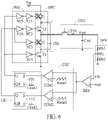
- FIG. 6 is a schematic diagram of flowing of a current of the power converter with the automatic balance mechanism of the flying capacitor when the first and third transistors of the power converter are turned off and the second and fourth transistors of the power converter are turned on according to the first embodiment of the present disclosure
- FIG. 7 is a waveform diagram of signals of the power converter with the automatic balance mechanism of the flying capacitor within a third time according to the first embodiment of the present disclosure.
- the first flip-flop FF 1 shown in FIG. 6 outputs the first logic signal D 1 at a low level for turning off the first transistor T 1 and turning on the fourth transistor T 4 during a time t 13 as shown in FIG. 7 .
- the second flip-flop FF 2 shown in FIG. 6 outputs the second logic signal D 2 at a high level for turning off the third transistor T 3 and turning on the second transistor T 2 during the time t 13 as shown in FIG. 7 .
- the current flowing indicating signal CFD 1 indicates that a current flows sequentially through the second transistor T 4 , the flying capacitor Cfly, and the second transistor T 2 to the output inductor L.
- the current of the inductor current signal IL gradually increases within the time t 13 .
- a working period of the first logic signal D 1 is the same as a working period of the second logic signal D 2 , such that a voltage of the flying capacitor Cfly is equal to one half of the input voltage Vin.
- Each of a slope of the first ramp signal Ramp 1 and a slope of the second ramp signal Ramp 2 is proportional to the voltage of the flying capacitor Cfly.
- a difference between the input voltage Vin received by the switch circuit SWC and the voltage of the flying capacitor Cfly is proportional to the slope of the first ramp signal Ramp 1 and the slope of the second ramp signal Ramp 2 .
- FIG. 8 is a circuit layout diagram of a power converter with an automatic balance mechanism of a flying capacitor according to a second embodiment of the present disclosure.
- the power converter with the automatic balance of the flying capacitor of the second embodiment may further include a ramp signal generator RAG.
- RAG ramp signal generator
- An output terminal of the ramp signal generator RAG is connected to the second input terminal such as the inverting input terminal of the first comparator COM 1 and the second input terminal such as the inverting input terminal of the second comparator COM 2 .
- the ramp signal generator RAG may output the first ramp signal Ramp 1 and the second ramp signal Ramp 2 respectively to the second input terminal of the first comparator COM 1 and the second input terminal of the second comparator COM 2 , according to the input voltage Vin and the voltage of the flying capacitor Cfly.
- FIG. 9 is a waveform diagram of signals generated by the power converter with the automatic balance mechanism of the flying capacitor when a ratio of a working period of a logic signal to a total time is smaller than 0.5 and a voltage of the flying capacitor is higher one half of an input voltage according to the second embodiment of the present disclosure.
- a ratio of a working period of the first logic signal D 1 to a total time of the first logic signal D 1 is smaller than 0.5
- a ratio of a working period of the second logic signal D 2 to a total time of the second logic signal D 2 is smaller than 0.5
- the working period of the second logic signal D 2 as shown in FIG. 9 that is outputted by the second flip flop FF 2 shown in FIG. 8 is larger than the working period of the first logic signal D 1 shown in FIG. 9 that is outputted by the first flip flop FF 1 shown in FIG. 8 .
- the voltage Vfly of the flying capacitor Cfly can be reduced to be equal to the one half of the input voltage Vin.
- FIG. 10 is a waveform diagram of signals generated by the power converter with the automatic balance mechanism of the flying capacitor when the ratio of the working period of the logic signal to the total time is smaller than 0.5 and the voltage of the flying capacitor is lower than one half of the input voltage according to the second embodiment of the present disclosure.
- the ratio of the working period of the first logic signal D 1 to the total time of the first logic signal D 1 is smaller than 0.5
- the ratio of the working period of the second logic signal D 2 to the total time of the second logic signal D 2 is smaller than 0.5.
- the working period of the first logic signal D 1 as shown in FIG. 10 that is outputted by the first flip flop FF 1 shown in FIG. 8 is larger than the working period of the second logic signal D 2 as shown in FIG. 10 that is outputted by the second flip flop FF 2 shown in FIG. 8 .
- the voltage Vfly of the flying capacitor Cfly can be increased to be equal to the one half of the input voltage Vin.
- FIG. 11 is a waveform diagram of signals generated by the power converter with the automatic balance mechanism of the flying capacitor when the ratio of the working period of the logic signal to the total time is larger than 0.5 and the voltage of the flying capacitor is higher than one half of the input voltage according to the second embodiment of the present disclosure.
- the ratio of the working period of the first logic signal D 1 to the total time of the first logic signal D 1 is larger than 0.5
- the ratio of the working period of the second logic signal D 2 to the total time of the second logic signal D 2 is larger than 0.5.
- a non-working period of the first logic signal D 1 as shown in FIG. 11 that is outputted by the first flip flop FF 1 shown in FIG. 8 is larger than a non-working period of the second logic signal D 2 as shown in FIG. 11 that is outputted by the second flip flop FF 2 shown in FIG. 8 .
- the voltage Vfly of the flying capacitor Cfly can be reduced to be equal to the one half of the input voltage Vin.
- FIG. 12 is a waveform diagram of signals generated by the power converter with the automatic balance mechanism of the flying capacitor when the ratio of the working period of the logic signal to the total time is larger than 0.5 and the voltage of the flying capacitor is lower than one half of the input voltage according to the second embodiment of the present disclosure.
- the ratio of the working period of the first logic signal D 1 to the total time of the first logic signal D 1 is smaller than 0.5
- the ratio of the working period of the second logic signal D 2 to the total time of the second logic signal D 2 is smaller than 0.5.
- a non-working period of the first logic signal D 1 as shown in FIG. 12 that is outputted by the first flip flop FF 1 shown in FIG. 8 is smaller than a non-working period of the second logic signal D 2 as shown in FIG. 12 that is outputted by the second flip flop FF 2 shown in FIG. 8 .
- the voltage Vfly of the flying capacitor Cfly can be increased to be equal to the one half of the input voltage Vin.
- the power converter with the automatic balance mechanism of the flying capacitor of the present disclosure adjusts the working period of the logic signals for controlling the switch circuit according to the ramp signal having a slope that is proportional to the voltage of the flying capacitor, such that the voltage of the flying capacitor is balanced to be equal to the one half of the input voltage.
Landscapes
- Engineering & Computer Science (AREA)
- Power Engineering (AREA)
- Dc-Dc Converters (AREA)
Abstract
Description
Claims (7)
Applications Claiming Priority (2)
| Application Number | Priority Date | Filing Date | Title |
|---|---|---|---|
| TW109124538A TWI766314B (en) | 2020-07-21 | 2020-07-21 | Power converter with automatic balance mechanism of flying capacitor |
| TW109124538 | 2020-07-21 |
Publications (2)
| Publication Number | Publication Date |
|---|---|
| US20220029534A1 US20220029534A1 (en) | 2022-01-27 |
| US11431246B2 true US11431246B2 (en) | 2022-08-30 |
Family
ID=79459266
Family Applications (1)
| Application Number | Title | Priority Date | Filing Date |
|---|---|---|---|
| US17/016,680 Active 2040-12-15 US11431246B2 (en) | 2020-07-21 | 2020-09-10 | Power converter with automatic balance mechanism of flying capacitor |
Country Status (3)
| Country | Link |
|---|---|
| US (1) | US11431246B2 (en) |
| CN (1) | CN113965077B (en) |
| TW (1) | TWI766314B (en) |
Families Citing this family (18)
| Publication number | Priority date | Publication date | Assignee | Title |
|---|---|---|---|---|
| US11502604B2 (en) * | 2019-11-22 | 2022-11-15 | Mediatek Inc. | Bang-bang flying capacitor voltage balance for buck converter |
| US20220255435A1 (en) * | 2021-02-08 | 2022-08-11 | Samsung Electronics Co., Ltd. | Bidirectional switching converter and operating method thereof |
| TWI764828B (en) * | 2021-09-10 | 2022-05-11 | 禾瑞亞科技股份有限公司 | Voltage doubling switched capacitor circuit capable of detecting short circuit of flying capacitor and detection method thereof |
| CN114614671B (en) * | 2022-03-04 | 2024-11-29 | 上海星思半导体有限责任公司 | Power supply suitable for 5GNR broadband high-efficiency envelope tracking power amplifier |
| IT202200007265A1 (en) * | 2022-04-12 | 2023-10-12 | St Microelectronics Srl | CONTROL MODULE FOR A RESONANT SWITCHED CAPACITY CONVERTER AND METHOD FOR CONTROLING A RESONANT SWITCHED CAPACITY CONVERTER |
| IT202200007685A1 (en) * | 2022-04-15 | 2023-10-15 | Milano Politecnico | DC-DC converter circuit and corresponding operating procedure |
| US11824463B1 (en) * | 2022-04-29 | 2023-11-21 | Novatek Microelectronics Corp. | Multiple output voltage generator |
| KR102626361B1 (en) * | 2022-05-18 | 2024-01-19 | 주식회사 실리콘마이터스 | 3 level buck-boost converter with flying capacitor voltage balancing circuit |
| CN115776228B (en) * | 2022-06-23 | 2025-09-09 | 圣邦微电子(苏州)有限责任公司 | DC-DC converter |
| CN115250061B (en) * | 2022-09-23 | 2023-01-06 | 深圳市微源半导体股份有限公司 | Voltage transformation circuit and electronic device |
| KR102616623B1 (en) * | 2022-12-06 | 2023-12-21 | (주)실리콘스타 | Flying capacitor balancing circuit in multi-level DC/DC converter and multi-level DC/DC converter having the same |
| US12395072B2 (en) | 2022-12-28 | 2025-08-19 | Delta Electronics, Inc. | Flying capacitor multi-level power factor correction converter of power supply with active balancing of voltage of flying capacitors |
| CN115833577B (en) * | 2023-02-08 | 2023-05-16 | 深圳市微源半导体股份有限公司 | Voltage conversion circuit and electronic equipment |
| CN116667650B (en) * | 2023-04-18 | 2024-02-20 | 华南理工大学 | A single-inductor multi-level DC converter based on adaptive slope calibration method |
| US12531467B2 (en) | 2023-05-03 | 2026-01-20 | Delta Electronics, Inc. | Single-stage bidirectional power supply |
| US12431802B2 (en) * | 2023-06-08 | 2025-09-30 | Richtek Technology Corp. | Multilevel buck converter with valley current mode control and dual slope compensation |
| KR102624425B1 (en) * | 2023-10-25 | 2024-01-12 | (주)실리콘스타 | Inductorless converter for wearable application |
| US20250239931A1 (en) * | 2024-01-22 | 2025-07-24 | Stmicroelectronics International N.V. | Balance system to regulate the voltage of the fly capacitor of a three-level buck acting on ramps |
Citations (9)
| Publication number | Priority date | Publication date | Assignee | Title |
|---|---|---|---|---|
| US20030214274A1 (en) * | 2002-05-14 | 2003-11-20 | Lethellier Patrice R. | Multiple-phase power converter having current sharing and high frequency filtering |
| US20130271214A1 (en) * | 2012-04-16 | 2013-10-17 | Nxp B.V. | Class d amplifiers |
| US20140063884A1 (en) * | 2012-08-29 | 2014-03-06 | Murata Manufacturing Co., Ltd. | Inverter device |
| US20160118887A1 (en) * | 2014-10-23 | 2016-04-28 | Qualcomm Incorporated | Circuits and methods for controlling a three-level buck converter |
| US20160329809A1 (en) * | 2015-05-05 | 2016-11-10 | Texas Instruments Incorporated | Multilevel boost dc to dc converter circuit |
| US9929653B1 (en) * | 2017-06-19 | 2018-03-27 | Dialog Semiconductor (Uk) Limited | Multi-level buck converter with multiple control loops and flying capacitor regulation |
| US10090763B1 (en) | 2017-06-19 | 2018-10-02 | Dialog Semiconductor (Uk) Limited | Multi-level buck converter having a regulated flying capacitor voltage used for high-side drive |
| US20190207519A1 (en) * | 2017-12-29 | 2019-07-04 | Texas Instruments Incorporated | Converter topology with adaptive power path architecture |
| US20200195133A1 (en) * | 2018-12-13 | 2020-06-18 | Infineon Technologies Ag | Flying capacitor balancing in a multi-level voltage converter |
Family Cites Families (14)
| Publication number | Priority date | Publication date | Assignee | Title |
|---|---|---|---|---|
| US7782027B2 (en) * | 2006-12-30 | 2010-08-24 | Advanced Analogic Technologies, Inc. | High-efficiency DC/DC voltage converter including down inductive switching pre-regulator and capacitive switching post-converter |
| US8427113B2 (en) * | 2007-08-01 | 2013-04-23 | Intersil Americas LLC | Voltage converter with combined buck converter and capacitive voltage divider |
| TWI425755B (en) * | 2010-07-21 | 2014-02-01 | Noveltek Semiconductor Corp | Pwm buck converter with surge reduction and related method |
| CN102055324A (en) * | 2011-01-11 | 2011-05-11 | 北方工业大学 | Power control device and method using integral circuit |
| JP5697621B2 (en) * | 2012-02-29 | 2015-04-08 | 株式会社東芝 | DC-DC converter and audio output device |
| TWI553605B (en) * | 2015-06-03 | 2016-10-11 | 矽創電子股份有限公司 | Power Supply System and Display Apparatus |
| US10637356B2 (en) * | 2017-04-03 | 2020-04-28 | Integrated Device Technology, Inc. | Multiple-level buck boost converter control |
| US20190058397A1 (en) * | 2017-08-15 | 2019-02-21 | Texas Instruments Incorporated | Harmonic modulation for charge balance of multi-level power converters |
| JP7001896B2 (en) * | 2017-11-10 | 2022-01-20 | オムロン株式会社 | DC-DC converter |
| WO2020024171A1 (en) * | 2018-08-01 | 2020-02-06 | 华为技术有限公司 | Control circuit for voltage conversion circuit |
| KR102606238B1 (en) * | 2018-11-05 | 2023-11-24 | 삼성전자주식회사 | Switching regulator generating continuous output delibery current and operating method thereof |
| US10811962B2 (en) * | 2018-11-20 | 2020-10-20 | Richtek Technology Corporation | Multi-level switching power converter, and controller circuit and control method thereof |
| US10944321B2 (en) * | 2018-11-20 | 2021-03-09 | Richtek Technology Corporation | Multi-level switching power converter, and controller circuit and control method thereof |
| US10615697B1 (en) * | 2019-02-27 | 2020-04-07 | Dialog Semiconductor (Uk) Limited | Multi-level switching converter with flying capacitor voltage regulation |
-
2020
- 2020-07-21 TW TW109124538A patent/TWI766314B/en active
- 2020-07-30 CN CN202010751569.7A patent/CN113965077B/en active Active
- 2020-09-10 US US17/016,680 patent/US11431246B2/en active Active
Patent Citations (10)
| Publication number | Priority date | Publication date | Assignee | Title |
|---|---|---|---|---|
| US20030214274A1 (en) * | 2002-05-14 | 2003-11-20 | Lethellier Patrice R. | Multiple-phase power converter having current sharing and high frequency filtering |
| US20130271214A1 (en) * | 2012-04-16 | 2013-10-17 | Nxp B.V. | Class d amplifiers |
| US20140063884A1 (en) * | 2012-08-29 | 2014-03-06 | Murata Manufacturing Co., Ltd. | Inverter device |
| US20160118887A1 (en) * | 2014-10-23 | 2016-04-28 | Qualcomm Incorporated | Circuits and methods for controlling a three-level buck converter |
| CN107636947A (en) | 2014-10-23 | 2018-01-26 | 高通股份有限公司 | For controlling the circuit and method of three-level buck converter |
| US20160329809A1 (en) * | 2015-05-05 | 2016-11-10 | Texas Instruments Incorporated | Multilevel boost dc to dc converter circuit |
| US9929653B1 (en) * | 2017-06-19 | 2018-03-27 | Dialog Semiconductor (Uk) Limited | Multi-level buck converter with multiple control loops and flying capacitor regulation |
| US10090763B1 (en) | 2017-06-19 | 2018-10-02 | Dialog Semiconductor (Uk) Limited | Multi-level buck converter having a regulated flying capacitor voltage used for high-side drive |
| US20190207519A1 (en) * | 2017-12-29 | 2019-07-04 | Texas Instruments Incorporated | Converter topology with adaptive power path architecture |
| US20200195133A1 (en) * | 2018-12-13 | 2020-06-18 | Infineon Technologies Ag | Flying capacitor balancing in a multi-level voltage converter |
Also Published As
| Publication number | Publication date |
|---|---|
| US20220029534A1 (en) | 2022-01-27 |
| CN113965077A (en) | 2022-01-21 |
| TW202205794A (en) | 2022-02-01 |
| CN113965077B (en) | 2024-10-18 |
| TWI766314B (en) | 2022-06-01 |
Similar Documents
| Publication | Publication Date | Title |
|---|---|---|
| US11431246B2 (en) | Power converter with automatic balance mechanism of flying capacitor | |
| US9595869B2 (en) | Multi-level switching regulator circuits and methods with finite state machine control | |
| US7961158B2 (en) | Constant-current driving circuit | |
| US8913404B2 (en) | Constant voltage constant current control circuits and methods with improved load regulation | |
| US7737767B2 (en) | Control circuit and control method for charge pump circuit | |
| US20150378378A1 (en) | Power converter and method for regulating line transient response of the power converter | |
| US20240235366A1 (en) | Switching converter and control circuit thereof | |
| US10447154B2 (en) | PWM control scheme for providing minimum on time | |
| US10050532B2 (en) | DC-DC converter with pseudo ripple voltage generation | |
| US10483837B1 (en) | Variable frequency modulation scheme based on current-sensing techniques for switched-capacitor DC-DC converters | |
| CN105207480A (en) | Synchronous buck DC-DC converter capable of achieving low output ripples in times of underloading | |
| EP4134778A1 (en) | Voltage regulating apparatus, chip, power supply, and electronic device | |
| US11258360B2 (en) | Switched-capacitor power converting apparatus and operating method thereof | |
| US12253872B2 (en) | Voltage adjustment apparatus, chip, power source, and electronic device | |
| US11863071B2 (en) | Power converter having smooth transition control mechanism | |
| US7400127B2 (en) | Method for regulating an output signal and circuit therefor | |
| US10770964B1 (en) | Overshoot reduction circuit for buck converter | |
| US20060028854A1 (en) | Charge pump circuit | |
| US20250373161A1 (en) | Multi-output power converter having single inductor | |
| US20240356428A1 (en) | Power converter having multi-mode switching mechanism | |
| CN119154664A (en) | Internal slope compensation for constant on-time buck converter | |
| US10382026B1 (en) | Phase shift control circuit for multi-channel system | |
| Li et al. | Fixed‐frequency adaptive on‐time buck converter with ramp compensation | |
| US20250239931A1 (en) | Balance system to regulate the voltage of the fly capacitor of a three-level buck acting on ramps | |
| US20260025054A1 (en) | Power converter of limiting negative current |
Legal Events
| Date | Code | Title | Description |
|---|---|---|---|
| FEPP | Fee payment procedure |
Free format text: ENTITY STATUS SET TO UNDISCOUNTED (ORIGINAL EVENT CODE: BIG.); ENTITY STATUS OF PATENT OWNER: SMALL ENTITY |
|
| FEPP | Fee payment procedure |
Free format text: ENTITY STATUS SET TO SMALL (ORIGINAL EVENT CODE: SMAL); ENTITY STATUS OF PATENT OWNER: SMALL ENTITY |
|
| AS | Assignment |
Owner name: ANPEC ELECTRONICS CORPORATION, TAIWAN Free format text: ASSIGNMENT OF ASSIGNORS INTEREST;ASSIGNOR:CHEN, FU-CHUAN;REEL/FRAME:054556/0797 Effective date: 20200908 |
|
| STPP | Information on status: patent application and granting procedure in general |
Free format text: NON FINAL ACTION MAILED |
|
| STPP | Information on status: patent application and granting procedure in general |
Free format text: RESPONSE TO NON-FINAL OFFICE ACTION ENTERED AND FORWARDED TO EXAMINER |
|
| STPP | Information on status: patent application and granting procedure in general |
Free format text: NOTICE OF ALLOWANCE MAILED -- APPLICATION RECEIVED IN OFFICE OF PUBLICATIONS |
|
| STPP | Information on status: patent application and granting procedure in general |
Free format text: PUBLICATIONS -- ISSUE FEE PAYMENT VERIFIED |
|
| STCF | Information on status: patent grant |
Free format text: PATENTED CASE |
|
| MAFP | Maintenance fee payment |
Free format text: PAYMENT OF MAINTENANCE FEE, 4TH YR, SMALL ENTITY (ORIGINAL EVENT CODE: M2551); ENTITY STATUS OF PATENT OWNER: SMALL ENTITY Year of fee payment: 4 |