US11417543B2 - Bonding apparatus and bonding method - Google Patents
Bonding apparatus and bonding method Download PDFInfo
- Publication number
- US11417543B2 US11417543B2 US16/508,507 US201916508507A US11417543B2 US 11417543 B2 US11417543 B2 US 11417543B2 US 201916508507 A US201916508507 A US 201916508507A US 11417543 B2 US11417543 B2 US 11417543B2
- Authority
- US
- United States
- Prior art keywords
- imaging
- holder
- substrate
- alignment mark
- processing
- Prior art date
- Legal status (The legal status is an assumption and is not a legal conclusion. Google has not performed a legal analysis and makes no representation as to the accuracy of the status listed.)
- Active
Links
Images


Classifications
-
- H—ELECTRICITY
- H10—SEMICONDUCTOR DEVICES; ELECTRIC SOLID-STATE DEVICES NOT OTHERWISE PROVIDED FOR
- H10P—GENERIC PROCESSES OR APPARATUS FOR THE MANUFACTURE OR TREATMENT OF DEVICES COVERED BY CLASS H10
- H10P72/00—Handling or holding of wafers, substrates or devices during manufacture or treatment thereof
- H10P72/04—Apparatus for manufacture or treatment
- H10P72/0428—Apparatus for mechanical treatment or grinding or cutting
-
- H01L21/67092—
-
- H01L21/2007—
-
- H01L21/6833—
-
- H—ELECTRICITY
- H10—SEMICONDUCTOR DEVICES; ELECTRIC SOLID-STATE DEVICES NOT OTHERWISE PROVIDED FOR
- H10P—GENERIC PROCESSES OR APPARATUS FOR THE MANUFACTURE OR TREATMENT OF DEVICES COVERED BY CLASS H10
- H10P10/00—Bonding of wafers, substrates or parts of devices
-
- H—ELECTRICITY
- H10—SEMICONDUCTOR DEVICES; ELECTRIC SOLID-STATE DEVICES NOT OTHERWISE PROVIDED FOR
- H10P—GENERIC PROCESSES OR APPARATUS FOR THE MANUFACTURE OR TREATMENT OF DEVICES COVERED BY CLASS H10
- H10P10/00—Bonding of wafers, substrates or parts of devices
- H10P10/12—Bonding of semiconductor wafers or semiconductor substrates to semiconductor wafers or semiconductor substrates
-
- H—ELECTRICITY
- H10—SEMICONDUCTOR DEVICES; ELECTRIC SOLID-STATE DEVICES NOT OTHERWISE PROVIDED FOR
- H10P—GENERIC PROCESSES OR APPARATUS FOR THE MANUFACTURE OR TREATMENT OF DEVICES COVERED BY CLASS H10
- H10P72/00—Handling or holding of wafers, substrates or devices during manufacture or treatment thereof
- H10P72/04—Apparatus for manufacture or treatment
- H10P72/0438—Apparatus for making assemblies not otherwise provided for, e.g. package constructions
-
- H—ELECTRICITY
- H10—SEMICONDUCTOR DEVICES; ELECTRIC SOLID-STATE DEVICES NOT OTHERWISE PROVIDED FOR
- H10P—GENERIC PROCESSES OR APPARATUS FOR THE MANUFACTURE OR TREATMENT OF DEVICES COVERED BY CLASS H10
- H10P72/00—Handling or holding of wafers, substrates or devices during manufacture or treatment thereof
- H10P72/06—Apparatus for monitoring, sorting, marking, testing or measuring
-
- H—ELECTRICITY
- H10—SEMICONDUCTOR DEVICES; ELECTRIC SOLID-STATE DEVICES NOT OTHERWISE PROVIDED FOR
- H10P—GENERIC PROCESSES OR APPARATUS FOR THE MANUFACTURE OR TREATMENT OF DEVICES COVERED BY CLASS H10
- H10P72/00—Handling or holding of wafers, substrates or devices during manufacture or treatment thereof
- H10P72/50—Handling or holding of wafers, substrates or devices during manufacture or treatment thereof for positioning, orientation or alignment
- H10P72/53—Handling or holding of wafers, substrates or devices during manufacture or treatment thereof for positioning, orientation or alignment using optical controlling means
-
- H—ELECTRICITY
- H10—SEMICONDUCTOR DEVICES; ELECTRIC SOLID-STATE DEVICES NOT OTHERWISE PROVIDED FOR
- H10P—GENERIC PROCESSES OR APPARATUS FOR THE MANUFACTURE OR TREATMENT OF DEVICES COVERED BY CLASS H10
- H10P72/00—Handling or holding of wafers, substrates or devices during manufacture or treatment thereof
- H10P72/50—Handling or holding of wafers, substrates or devices during manufacture or treatment thereof for positioning, orientation or alignment
- H10P72/57—Mask-wafer alignment
-
- H—ELECTRICITY
- H10—SEMICONDUCTOR DEVICES; ELECTRIC SOLID-STATE DEVICES NOT OTHERWISE PROVIDED FOR
- H10P—GENERIC PROCESSES OR APPARATUS FOR THE MANUFACTURE OR TREATMENT OF DEVICES COVERED BY CLASS H10
- H10P72/00—Handling or holding of wafers, substrates or devices during manufacture or treatment thereof
- H10P72/70—Handling or holding of wafers, substrates or devices during manufacture or treatment thereof for supporting or gripping
- H10P72/72—Handling or holding of wafers, substrates or devices during manufacture or treatment thereof for supporting or gripping using electrostatic chucks
- H10P72/722—Details of electrostatic chucks
-
- H—ELECTRICITY
- H10—SEMICONDUCTOR DEVICES; ELECTRIC SOLID-STATE DEVICES NOT OTHERWISE PROVIDED FOR
- H10P—GENERIC PROCESSES OR APPARATUS FOR THE MANUFACTURE OR TREATMENT OF DEVICES COVERED BY CLASS H10
- H10P90/00—Preparation of wafers not covered by a single main group of this subclass, e.g. wafer reinforcement
- H10P90/19—Preparing inhomogeneous wafers
- H10P90/1904—Preparing vertically inhomogeneous wafers
- H10P90/1906—Preparing SOI wafers
- H10P90/1914—Preparing SOI wafers using bonding
Definitions
- Patent Document 1 discloses a bonding apparatus in which a first substrate is held by a first holder, a second substrate is held by a second holder placed to face the first holder, and the first substrate and the second substrate are bonded by bringing the first holder and the second holder close to each other.
- Patent Document 1 Japanese Patent Laid-open Publication No. 2016-134446
- Exemplary embodiments provide a technique capable of suppressing a position deviation between substrates in a bonding apparatus configured to bond the substrates.
- a bonding apparatus in one exemplary embodiment, includes a first holder, a second holder, an imaging unit and a moving device.
- the first holder is configured to hold a first substrate.
- the second holder is disposed to face the first holder and configured to hold a second substrate to be bonded to the first substrate.
- the imaging unit includes a first imaging device configured to image a first alignment mark formed on a surface of the first substrate facing the second substrate and a second imaging device configured to image a second alignment mark formed on a surface of the second substrate facing the first substrate.
- the moving device is configured to move the imaging unit in a first direction and a second direction intersecting with the first direction within a plan region between the first holder and the second holder.
- FIG. 1 is a diagram illustrating a configuration example of a bonding system according to an exemplary embodiment
- FIG. 2 is a diagram illustrating a configuration example of a vacuum bonding block according to the exemplary embodiment
- FIG. 3 is a diagram illustrating a configuration example of a vacuum bonding apparatus according to the exemplary embodiment
- FIG. 4 is a diagram illustrating the configuration example of the vacuum bonding apparatus according to the exemplary embodiment
- FIG. 5 is a diagram illustrating a configuration example of an imaging unit
- FIG. 6 is a flowchart illustrating an example of a sequence of a series of processings performed in the vacuum bonding apparatus
- FIG. 7 is a diagram illustrating an operation example of a wide-area imaging processing
- FIG. 8 is a diagram illustrating an operation example of a pre-alignment processing
- FIG. 9 is a diagram illustrating an operation example of a first chuck mark imaging processing
- FIG. 10 is a diagram illustrating an operation example of a second chuck mark imaging processing.
- FIG. 11 is a diagram illustrating an operation example of a second fine alignment processing.
- FIG. 1 is a diagram illustrating the configuration example of the bonding system according to the exemplary embodiment.
- the X-axis, Y-axis and Z-axis which are orthogonal to each other will be defined.
- the positive Z-axis direction will be regarded as a vertically upward direction.
- a bonding system 100 according to the exemplary embodiment shown in FIG. 1 is configured to produce a combined substrate T by bonding a first substrate W 1 and a second substrate W 2 .
- the bonding system 100 includes a carry-in/out block 1 , a delivery block 2 , a transfer block 3 , a surface processing block 4 , a normal pressure bonding block 5 and a vacuum bonding block 6 .
- the carry-in/out block 1 is equipped with a placing table 7 and a transfer region 8 .
- the placing table 7 is equipped with a plurality of (e.g., four) cassette placing plates 101 .
- Cassettes C 1 to C 4 are placed on the cassette placing plates 101 , respectively.
- Each of the cassettes C 1 to C 4 is configured to accommodate therein a plurality of (e.g., 25 sheets of) substrates horizontally.
- the cassette C 1 accommodates a plurality of first substrates W 1 ; the cassette C 2 , a plurality of second substrates W 2 ; and the cassettes C 3 , a plurality of combined substrates T.
- the cassette C 4 is provided to accommodate, for example, a substrate which has a problem.
- the transfer region 8 is disposed adjacent to the placing table 7 .
- a transfer path 102 extended in the Y-axis direction and a transfer device 103 configured to be movable along this transfer path 102 are provided in the transfer region 8 .
- the transfer device 103 is also movable in the X-axis direction and pivotable around the Z-axis, and carries the first substrate W 1 , the second substrate W 2 and the combined substrate T to/from the cassettes C 1 to C 4 and the delivery block 2 .
- the delivery block 2 is disposed adjacent to the carry-in/out block 1 .
- the delivery block 2 is equipped with a transit table 104 .
- the transit table 104 is configured to accommodate a plurality of the first substrates W 1 , the second substrates W 2 and the combined substrates T in multiple levels.
- the transfer block 3 is disposed adjacent to the delivery block 2 .
- the transfer block 3 is equipped with a transfer path 105 extended in, for example, the X-axis direction and a transfer device 106 configured to be movable along this transfer path 105 .
- the transfer device 106 is also movable in the Y-axis direction and pivotable around the Z-axis, and carries the first substrate W 1 , the second substrate W 2 and the combined substrate T to/from the delivery block 2 , the surface processing block 4 , the normal pressure bonding block 5 and the vacuum bonding block 6 .
- the surface processing block 4 , the normal pressure bonding block 5 and the vacuum bonding block 6 are disposed adjacent to the transfer block 3 .
- the surface hydrophilizing apparatus is configured to supply a hydrophilic processing liquid such as pure water to bonding surfaces of the first substrate W 1 and the second substrate W 2 to thereby hydrophilize these bonding surfaces.
- the surface modifying apparatus is configured to modify the bonding surfaces of the first substrate W 1 and the second substrate W 2 by plasma of a processing gas.
- a normal pressure bonding apparatus Disposed in the normal pressure bonding block 5 is a normal pressure bonding apparatus configured to bond the first substrate W 1 and the second substrate W 2 in a normal pressure atmosphere.
- configurations of the surface hydrophilizing apparatus, the surface modifying apparatus and the normal pressure bonding apparatus are not particularly limited, configurations of a surface hydrophilizing apparatus, a surface modifying apparatus and a bonding apparatus described in, for example, Japanese Patent No. 6,040,123 may be used.
- a vacuum bonding apparatus Disposed in the vacuum bonding block 6 is a vacuum bonding apparatus configured to bond the first substrate W 1 and the second substrate W 2 in a decompressed atmosphere. Configurations of the vacuum bonding block 6 and the vacuum bonding apparatus will be discussed later.
- the bonding system 100 is equipped with a control device 200 .
- the control device 200 controls an operation of the bonding system 100 .
- This control device 200 may be, for example, a computer and is equipped with a non-illustrated controller and a non-illustrated storage.
- the storage is composed of a storage device such as, but not limited to, a RAM (Random Access Memory), a ROM (Read Only Memory) or a hard disk, and stores therein a program for controlling various processings such as a bonding processing.
- the controller may be, by way of example, but not limitation, a CPU (Central Processing unit) and controls the operation of the bonding system 100 by reading out and executing the program stored in the storage.
- a CPU Central Processing unit
- the program may be recorded on a computer-readable recording medium and installed from this recording medium to the storage of the control device 200 .
- the computer-readable recording medium may be, by way of non-limiting example, a hard disk (HD), a flexible disk (FD), a compact disk (CD), a magnet optical disk (MO), a memory card, or the like.
- FIG. 2 is a diagram illustrating the configuration example of the vacuum bonding block 6 according to the exemplary embodiment.
- the vacuum bonding block 6 is equipped with a delivery unit 108 , a transfer device 109 and a vacuum bonding apparatus 110 .
- the delivery unit 108 is disposed between the transfer block 3 and the transfer device 109 .
- the delivery unit 108 is capable of holding the first substrate W 1 , the second substrate W 2 and the combined substrate T.
- the delivery unit 108 is equipped with an attracting/holding unit configured to attract and hold the first substrate W 1 from above and a plurality of (e.g., three) supporting pins configured to support the second substrate W 2 from below.
- the transfer device 106 provided in the transfer block 3 transfers the first substrate W 1 to the attracting/holding unit of the delivery unit 108 with the bonding surface of the first substrate W 1 facing downwards.
- the transfer device 106 transfers the second substrate W 2 to the plurality of supporting pins of the delivery unit 108 with the bonding surface of the second substrate W 2 facing upwards. Furthermore, the transfer device 106 receives the combined substrate T delivered onto the plurality of supporting pins of the delivery unit 108 by the transfer device 109 to be described later and transfers the received combined substrate T to the transit table 104 of the transfer block 2 .
- the transfer device 109 is equipped with an arm configured to be extensible/contractible in the horizontal direction and a base configured to be pivotable around the Z-axis.
- the transfer device 109 performs a carry-in/carry-out of the first substrate W 1 , the second substrate W 2 and the combined substrate T with respect to the delivery unit 108 and the vacuum bonding apparatus 110 .
- the transfer device 109 receives the first substrate W 1 , which is held by the attracting/holding unit of the delivery unit 108 , from the delivery unit 108 by supporting the first substrate W 1 from below, and carries the received first substrate W 1 into the vacuum bonding apparatus 110 . Further, the transfer device 109 receives from the delivery unit 108 the second substrate W 2 , which is supported by the supporting pins of the delivery unit 108 , by supporting the second substrate W 2 from below, and carries the received second substrate W 2 into the vacuum bonding apparatus 110 . Furthermore, the transfer device 109 takes out the combined substrate T from the vacuum bonding apparatus 110 and delivers it onto the supporting pins of the delivery unit 108 .
- the vacuum bonding apparatus 110 is equipped with a chamber 10 capable of forming a sealed processing space therein.
- the vacuum bonding apparatus 110 decompresses the chamber 10 after accommodating the first substrate W 1 and the second substrate W 2 in the chamber 10 . Then, the vacuum bonding apparatus 110 bonds the first substrate W 1 and the second substrate W 2 in a decompressed atmosphere.
- the vacuum bonding apparatus 110 is further equipped with: an imaging unit 50 configured to image alignment marks provided on the bonding surfaces of the first substrate W 1 and the second substrate W 2 ; and a moving device 60 configured to move the imaging unit 50 .
- the moving device 60 is capable of moving the imaging unit 50 in the X-axis direction and is also capable of moving the imaging unit 50 in the Y-axis direction.
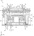
- FIG. 3 and FIG. 4 are diagrams illustrating a configuration example of the vacuum bonding apparatus 110 according to the exemplary embodiment.
- FIG. 3 illustrates the vacuum bonding apparatus 110 seen along the X-axis direction
- FIG. 4 illustrates the vacuum bonding apparatus 110 seen along the Y-axis direction.
- the vacuum bonding apparatus 110 includes the chamber 10 , a first holder 20 , a second holder 30 , an elevator 40 , the imaging unit 50 , the moving device 60 , a plurality of third imaging devices 70 and a plurality of light sources 80 .
- the chamber 10 is equipped with a first vessel 11 , a second vessel 12 and an opening/closing device 13 .
- the first vessel 11 has a concave shape with a side thereof facing the second holder 30 opened (that is, an open bottom), and the first holder 20 is accommodated in this first vessel 11 .
- the second vessel 12 has a concave shape with a side facing the first holder 20 opened (that is, an open top), and the second holder 30 is accommodated in this second vessel 12 .
- the opening/closing device 13 is configured to move the first vessel 11 in the vertical direction. In this chamber 10 , by moving the first vessel 11 with the opening/closing device 13 to be brought into contact with the second vessel 12 , the sealed processing space is formed within the chamber 10 .
- a multiple number of through holes 111 is vertically formed through a ceiling of the first vessel 11 . These through holes 111 are formed to be located at an outer position than the first holder 20 in a radial direction. Each through hole 111 is closed by a transparent member 112 .
- the transparent member 112 is made of, by way of non-limiting example, quartz glass and disposed in a lower portion of the through hole 111 to be located near the processing space.
- a multiple number of through holes 121 is vertically formed through a bottom of the second vessel 12 . These through holes 121 are formed to be located at an outer position than the second holder 30 in a radial direction to directly face the through holes 111 . Each through hole 121 is closed by a transparent member 122 .
- the transparent member 122 is made of, by way of non-limiting example, quartz glass or the like.
- a through hole 123 is vertically formed through a center of the bottom of the second vessel 12 .
- a shaft 31 to be described later is inserted through this through hole 123 .
- one end of a cylindrical bellows 124 is connected to a center of a bottom surface of the second vessel 12 .
- the bellows 124 is configured to surround the through hole 123 .
- the other end of the bellows 124 is connected to a top surface of a supporting plate 41 of the elevator 40 to be described later.
- An exhaust pipe 16 for evacuating the chamber 10 is connected to the bottom of the second vessel 12 .
- the exhaust pipe 16 is connected to an exhaust device 17 such as a vacuum pump.
- the opening/closing device 13 is equipped with a plurality of (e.g., two) shafts 131 and a plurality of drivers 132 .
- Each shaft 131 is vertically extended, and a leading end thereof is connected to a flange 113 protruded outwards from an outer edge of the first vessel 11 .
- the driver 132 moves the shaft 131 in the vertical direction.
- the driver 132 is fixed to a top surface of a base plate 14 provided under the second vessel 12 .
- the first holder 20 is a holder configured to attract and hold the first substrate W 1 , and is accommodated within the first vessel 11 with a holding surface thereof facing downwards.
- the first substrate W 1 is held by the first holder 20 with the bonding surface to be bonded to the second substrate W 2 facing downwards.
- the first holder 20 has, for example, a non-illustrated internal electrode, and is capable of attracting the first substrate W 1 to the holding surface by using an electrostatic force generated by applying a voltage to the internal electrode. Further, the first holder 20 may be connected to a non-illustrated evacuating device such as a vacuum pump via a non-illustrated evacuation pipe, and may attract the first substrate W 1 to the holding surface by an evacuating force generated by the evacuating device.
- a non-illustrated evacuating device such as a vacuum pump via a non-illustrated evacuation pipe
- An adjuster 21 configured to adjust a horizontal position of the first holder 20 is provided at an upper portion of the first holder 20 .
- the adjuster 21 is capable of moving the first holder 20 in the X-axis direction or in the Y-axis direction. Further, the adjuster 21 is also capable of rotating the first holder 20 around the vertical axis. That is, the adjuster 21 is capable of changing a direction of the first holder 20 in the horizontal direction.
- a plurality of transparent members 22 is provided at an outer edge of the first holder 20 .
- Each transparent member 22 is made of, by way of example, quartz glass or the like.
- An alignment mark (hereinafter, referred to as “first chuck mark”) for use in a second fine alignment processing to be described later is formed at each transparent member 22 by, for example, metal deposition or the like.
- the second holder 30 is a holder configured to attract and hold the second substrate W 2 , and is accommodated within the second vessel 12 with a holding surface thereof facing upwards.
- the second substrate W 2 is held by the second holder 30 with the bonding surface to be bonded to the first substrate W 1 facing upwards.
- the second holder 30 may attract the second substrate W 2 to the holding surface thereof by using the electrostatic force or the evacuating force.
- a leading end of the shaft 31 which is extended in the vertical direction is connected to a lower portion of the second holder 30 .
- the shaft 31 is inserted through the through hole 123 of the second vessel 12 and is covered by the bellows 124 .
- a lower end of the shaft 31 is connected to the supporting plate 41 of the elevator 40 to be described later.
- a plurality of transparent members 32 is provided at an outer edge of the second holder 30 .
- Each transparent member 32 is made of, by way of example, quartz glass or the like.
- a second chuck mark for use in the second fine alignment processing to be described later is formed at each transparent member 32 by, for example, metal deposition or the like.
- the elevator 40 is equipped with the supporting plate 41 , a plurality of supporting column members 42 and a plurality of drivers 43 .
- the supporting plate 41 is a flat plate disposed between the second vessel 12 and the base plate 14 .
- Leading ends of the supporting column members 42 are connected to the supporting plate 41 , and the other ends of the supporting column members 42 are respectively connected to the drivers 43 .
- Each driver 43 is configured to move the corresponding supporting column member 42 in the vertical direction.
- the drivers 43 are fixed to the base plate 14 .
- the elevator 40 moves up the supporting column members 42 and the supporting plate 41 by using the plurality of drivers 43 , thus raising the shaft 31 connected to the supporting plate 41 and the second holder 30 connected to the shaft 31 . Further, the elevator 40 is capable of adjusting a degree of horizontality of the second holder 30 by moving the plurality of supporting column members 42 individually.
- the imaging unit 50 images the alignment mark provided on the first substrate W 1 and the alignment mark provided on the second substrate W 2 .
- a configuration of the imaging unit 50 will be elaborated with reference to FIG. 5 .
- FIG. 5 is a diagram illustrating the configuration example of the imaging unit.
- the imaging unit 50 includes a first imaging device 51 , a second imaging device 52 , a first displacement sensor 53 and a second displacement sensor 54 , which are configured as a single body.
- the first imaging device 51 images a first alignment mark provided on a bottom surface of the first substrate W 1 .
- the first imaging device 51 includes a first wide-area imaging module 511 and a first local imaging module 512 .
- the first wide-area imaging module 511 is equipped with a first wide-area objective lens 513 and a first wide-area focusing device 514 configured to adjust a height position of the first wide-area objective lens 513 .
- the first local imaging module 512 is equipped with a first local objective lens 515 and a first local focusing device 516 configured to adjust a height position of the first local objective lens 515 .
- the first wide-area objective lens 513 is, for example, a macro lens
- the first local objective lens 515 is a micro lens having a magnification higher than that of the first wide-area objective lens 513 .
- the first imaging device 51 is capable of imaging the bottom surface of the first substrate W 1 in a relatively wide range by using the first wide-area imaging module 511 . Further, the first imaging device 51 is capable of imaging the first alignment mark provided on the bottom surface of the first substrate W 1 by using the first local imaging module 512 with higher accuracy than in case of using the first wide-area imaging module 511 . Further, the first imaging device 51 is capable of focusing the first wide-area objective lens 513 and the first local objective lens 515 on the bottom surface of the first substrate W 1 by using the first wide-area focusing device 514 and the first local focusing device 516 .
- the second imaging device 52 images a second alignment mark provided on the top surface of the second substrate W 2 .
- the second imaging device 52 includes a second wide-area imaging module 521 and a second local imaging module 522 .
- the second wide-area imaging module 521 is equipped with a second wide-area objective lens 523 and a second wide-area focusing device 524 configured to adjust a height position of the second wide-area objective lens 523 .
- the second local imaging module 522 is equipped with a second topical objective lens 525 and a second local focusing device 526 configured to adjust a height position of the second topical objective lens 525 .
- the second wide-area objective lens 523 may be, by way of example, but not limitation, a macro lens, and the second topical objective lens 525 is a micro lens having a magnification higher than that of the second wide-area objective lens 523 .
- the second imaging device 52 is capable of imaging the top surface of the second substrate W 2 in a relatively wide range by using the second wide-area imaging module 521 . Further, the second imaging device 52 is also capable of imaging the second alignment mark provided on the top surface of the second substrate W 2 by using the second local imaging module 522 with higher accuracy than in case of using the second wide-area imaging module 521 . Furthermore, the second imaging device 52 is capable of focusing the second wide-area objective lens 523 and the second topical objective lens 525 on the top surface of the second substrate W 2 by using the second wide-area focusing device 524 and the second local focusing device 526 .
- the first wide-area imaging module 511 and the first local imaging module 512 are fastened to a mount 65 of the moving device 60 to be describe later with the first wide-area objective lens 513 and the first local objective lens 515 facing upwards.
- the second wide-area imaging module 521 and the second local imaging module 522 are fastened to the mount 65 of the moving device 60 to be described later to be vertically symmetrical with respect to the first wide-area imaging module 511 and the first local imaging module 512 . That is, the second wide-area imaging module 521 is placed under the first wide-area imaging module 511 with the second wide-area objective lens 523 facing downwards. Further, the second local imaging module 522 is disposed under the first local imaging module 512 with the second topical objective lens 525 facing downwards.
- the imaging unit 50 is configured as stated above, and is capable of imaging the first alignment mark provided on the first substrate W 1 and the second alignment mark provided on the second substrate W 2 at the same time by using the first imaging device 51 and the second imaging device 52 .
- An optical axis of the first wide-area objective lens 513 belonging to the first wide-area imaging module 511 and an optical axis of the second wide-area objective lens 523 belonging to the second wide-area imaging module 521 are both vertically extended and lie on the same straight line. Accordingly, when a region on the first substrate W 1 centered on certain coordinates is imaged by the first wide-area imaging module 511 , for example, a region on the second substrate W 2 centered on the same coordinates can be imaged by the second wide-area imaging module 521 . Thus, in the pre-alignment processing to be described later, it is easy to perform a processing of aligning the position of the first alignment mark provided on the first substrate W 1 with the position of the second alignment mark provided on the second substrate W 2 .
- an optical axis of the first local objective lens 515 belonging to the first local imaging module 512 and an optical axis of the second topical objective lens 525 belonging to the second local imaging module 522 are both vertically extended and lie on the same straight line. Accordingly, when a region on the first substrate W 1 centered on certain coordinates is imaged by the first local imaging module 512 , for example, a region on the second substrate W 2 centered on the same coordinates can be imaged by the second local imaging module 522 . Thus, in the first fine alignment processing to be described later, it is easy to perform a processing of aligning the position of the first alignment mark provided on the first substrate W 1 with the position of the second alignment mark provided on the second substrate W 2 .
- the first displacement sensor 53 and the second displacement sensor 54 are, for example, displacement meters.
- the first displacement sensor 53 measures a distance to the bottom surface of the first substrate W 1 by irradiating laser light to the bottom surface of the first substrate W 1 and receiving reflection light thereof.
- the second displacement sensor 54 measures a distance to the top surface of the second substrate W 2 by irradiating laser light to the top surface of the second substrate W 2 and receiving reflection light thereof.
- the first displacement sensor 53 is disposed between the first wide-area imaging module 511 and the first local imaging module 512
- the second displacement sensor 54 is disposed between the second wide-area imaging module 521 and the second local imaging module 522 .
- the moving device 60 moves the imaging unit 50 in the X-axis direction and the Y-axis direction in a plan region between the first holder 20 and the second holder 30 .
- the alignment mark may not always be provided on the same position with respect to the substrate.
- the alignment mark may be provided on a periphery of the substrate or a position inner than that. According to the vacuum bonding apparatus 110 of the present exemplary embodiment, even when the alignment mark is provided on a certain position, the imaging unit 50 can be moved to the corresponding position by using the moving device 60 .
- the moving device 60 moves the first imaging device 51 and the second imaging device 52 as one body, a deviation in imaging positions between the first imaging device 51 and the second imaging device 52 which might be caused by a movement thereof may hardly occur.
- the moving device 60 has a door shape, and is equipped with a pair of first extending members 61 , a pair of legs 62 , a pair of first drivers 63 , a second extending member 64 , the mount 65 and a second driver 66 .
- the pair of the first extending members 61 include, by way of example, a ball screw and a linear guide.
- the pair of the first extending members 61 is fixed on the base plate 14 and extended in the X-axis direction.
- the pair of the first extending members 61 is disposed at an outer position than the chamber 10 and an inner position than the opening/closing device 13 .
- one of the first extending members 61 is disposed at a negative Y-axis side of the chamber 10 and a positive Y-axis side of the opening/closing device 13
- the other first extending member 61 is disposed at a positive Y-axis side of the chamber 10 and a negative Y-axis side of the opening/closing device 13 .
- the pair of legs 62 is vertically extended and is connected to the pair of first extending members 61 .
- Each of the first drivers 63 includes, for example, a motor. The first drivers 63 move the pair of legs 62 along the first extending members 61 .
- the second extending member 64 includes, by way of example, a ball screw, a linear guide, and so forth.
- the second extending member 64 is extended along the Y-axis direction by being suspended by the pair of legs 62 .
- the mount 65 is connected to the second extending member 64 .
- the imaging unit 50 is fastened to the mount 65 .
- the second driver 66 includes, by way of example, a motor and moves the mount 65 and the imaging unit 50 fastened to the mount 65 along the second extending member 64 .
- the imaging unit 50 can be moved between an imaging position between the first holder 20 and the second holder 30 and a retreat position at an outside of the chamber 10 . Further, with this moving device 60 , by moving the pair of legs 62 in the X-axis direction and the mount 65 in the Y-axis direction, the imaging unit 50 can be placed at various imaging positions in the plan region between the first holder 20 and the second holder 30 .
- each of the third imaging devices 70 is connected to an upper portion of the first vessel 11 of the chamber 10 with an elevator 71 therebetween.
- the elevator 71 adjusts a height position of the third imaging device 70 .
- the third imaging device 70 has an objective lens 72 . At least a part of the objective lens 72 is placed within the through hole 111 formed through the first vessel 11 .
- the through holes 111 are provided through the first vessel 11 , and the objective lenses 72 of the third imaging devices 70 are disposed within the through holes 111 . Accordingly, the objective lenses 72 can be made to be placed closer to the first chuck mark and the second chuck mark on the transparent members 22 and 32 as observation targets. Thus, even if a focal length of the objective lenses 72 is short, the objective lenses 72 can be appropriately focused on the first chuck mark and the second chuck mark.
- Each third imaging device 70 is configured to image the first chuck mark formed on the transparent member 22 through the transparent member 112 . Further, the third imaging device 70 images the second chuck mark on the transparent member 32 through the transparent member 112 and the transparent member 22 .
- Each light source 80 is disposed under the second vessel 12 within the chamber 10 with an optical axis thereof facing vertically upwards.
- the light source 80 irradiates light to the inside of the processing space via the transparent member 122 .
- the light irradiated from the light source 80 may be, by way of non-limiting example, infrared light. Further, the light irradiated from the light source 80 may be laser light.
- the light irradiated from the light source 80 to the inside of the processing space via the transparent member 122 arrives at the objective lens 72 of the third imaging device 70 via the transparent member 32 , the transparent member 22 and the transparent member 112 .
- FIG. 6 is a flowchart showing an example of the series of processings performed in the vacuum bonding apparatus 110 .
- FIG. 7 is a diagram illustrating an example operation of a wide-area imaging processing
- FIG. 8 is a diagram illustrating an example operation of a pre-alignment processing.
- FIG. 9 is a diagram illustrating an operation example of a first chuck mark imaging processing
- FIG. 10 is a diagram illustrating an operation example of a second chuck mark imaging processing.
- FIG. 11 is a diagram illustrating an operation example of a second fine alignment processing.
- each processing shown in FIG. 6 is performed as the controller of the control device 200 reads out the program stored in the storage of the control device 200 and controls the vacuum bonding apparatus 110 based on the read command. Further, FIG. 6 shows the sequence of the respective processings performed after the first substrate W 1 is held by the first holder 20 and the second substrate W 2 is held by the second holder 30 . Prior to the start of a process S 101 , the chamber 10 is in an open state, that is, in a state where the first vessel 11 is raised.
- a thickness measurement processing is first performed (process S 101 ).
- the imaging unit 50 is moved to a thickness measurement position between the first holder 20 and the second holder 30 from the retreat position at the outside of the chamber 10 .
- the distance from the imaging unit 50 to the bottom surface of the first substrate W 1 is measured by using the first displacement sensor 53
- the distance from the imaging unit 50 to the top surface of the second substrate W 2 is measured by using the second displacement sensor 54 .
- Measurement results by the first displacement sensor 53 and the second displacement sensor 54 are outputted to the control device 200 .
- the control device 200 calculates a thickness of the first substrate W 1 by using the measurement result from the first displacement sensor 53 and a previously acquired distance from the imaging unit 50 to the holding surface of the first holder 20 . Likewise, the control device 200 calculates a thickness of the second substrate W 2 by using the measurement result from the second displacement sensor 54 and a previously acquired distance from the imaging unit 50 to the holding surface of the second holder 30 .
- a wide-area imaging processing is performed (process S 102 ).
- the second wide-area imaging module 521 of the imaging unit 50 is moved to a preset imaging position corresponding to, for example, a position of the second substrate W 2 where a second alignment mark M 2 is formed.
- a first alignment mark M 1 of the first substrate W 1 is imaged by using the first wide-area imaging module 511 of the imaging unit 50
- a pre-alignment processing is performed in the vacuum bonding apparatus 110 (process S 103 ).
- the horizontal position of the first holder 20 is adjusted by controlling the adjuster 21 based on the imaging results of the first wide-area imaging module 511 and the second wide-area imaging module 521 (see FIG. 8 ).
- the first alignment mark M 1 has a cross shape
- the second alignment mark M 2 has a shape obtained by cutting the inside of the rectangle in the cross shape.
- the pre-alignment processing by adjusting the horizontal position of the first holder 20 by using the adjuster 21 , the cross shape of the first alignment mark M 1 and the cross shape of the second alignment mark M 2 are overlapped.
- the processings of the process S 102 and the process S 103 may be repeated multiple times until a deviation between the position of the first alignment mark M 1 and the position of the second alignment mark M 2 falls within a threshold value.
- a local imaging processing is performed (process S 104 ).
- the second local imaging module 522 of the imaging unit 50 is moved to, for example, the position of the second alignment mark M 2 detected in the wide-area imaging processing.
- the first alignment mark M 1 provided on the bottom surface of the first substrate W 1 is imaged by using the first local imaging module 512 of the imaging unit 50 .
- the second alignment mark M 2 provided on the top surface of the second substrate W 2 is imaged by using the second local imaging module 522 of the imaging unit 50 . Imaging results of the first local imaging module 512 and the second local imaging module 522 are outputted to the control device 200 .
- a first fine alignment processing is performed (process S 105 ).
- the horizontal position of the first holder 20 is further adjusted by controlling the adjuster 21 based on the imaging results of the first local imaging module 512 and the second local imaging module 522 . Accordingly, the first substrate W 1 and the second substrate W 2 come into a position-determined state. Further, the processings of the process S 104 and the process S 105 may be repeated multiple times until the deviation between the position of the first alignment mark M 1 and the position of the second alignment mark M 2 falls within the threshold value.
- a first chuck mark imaging processing is carried out (process S 106 ).
- the first chuck mark imaging processing by using the moving device 60 , the second local imaging module 522 of the imaging unit 50 is moved to, for example, a preset imaging position corresponding to a position where a second chuck mark M 4 of the transparent member 32 is formed. Then, a first chuck mark M 3 of the transparent member 22 is imaged by using the first local imaging module 512 of the imaging unit 50 , and the second chuck mark M 4 of the transparent member 32 is imaged by using the second local imaging module 522 (see FIG. 9 ).
- Imaging results of the first local imaging module 512 and the second local imaging module 522 are outputted to the control device 200 and stored in the storage as information showing a positional relationship between the first chuck mark M 3 and the second chuck mark M 4 in the state that the positioning of the first substrate W 1 and the second substrate W 2 is completed.
- a retreat processing is performed (process S 107 ).
- the imaging unit 50 is moved to the retreat position at the outside of the chamber 10 by using the moving device 60 .
- a chamber closing processing is performed (process S 108 ).
- the chamber closing processing by lowering the first vessel 11 by using the opening/closing device 13 , the first vessel 11 is brought into contact with the second vessel 12 . Accordingly, the sealed processing space is formed within the first vessel 11 .
- the first substrate W 1 held by the first holder 20 is made to come close to the second substrate W 2 held by the second holder 30 but without being in contact with the second substrate W 2 .
- a decompress processing is performed (process S 109 ).
- the decompress processing by evacuating the chamber 10 through the exhaust device 17 , the processing space is decompressed. Accordingly, the inside of the chamber 10 of the vacuum bonding apparatus 110 is turned into a high vacuum state equal to or less than, e.g., 0.005 Pa.
- an approach processing is performed (process S 110 ).
- the second holder 30 is moved up by using the elevator 40 so that the gap between the first substrate W 1 and the second substrate W 2 has a predetermined value (e.g., 100 ⁇ m).
- a distance by which the second holder 30 is raised is determined based on the thicknesses of the first substrate W 1 and the second substrate W 2 measured in the thickness measurement processing of the process S 101 .
- the chamber closing processing if a moving direction of the first vessel 11 is deviated from the vertical direction, the horizontal position of the first substrate W 1 is deviated. As a result, the position-determined state of the first substrate W 1 and the second substrate W 2 in the first fine alignment processing may be disturbed. In the approach processing, the same problem may occur if a moving direction of the second vessel 12 is deviated from the vertical direction. As a resolution, the second chuck mark imaging processing and the second fine alignment processing to be described later are performed in the vacuum bonding apparatus 110 .
- the second chuck mark imaging processing is performed (process S 111 ).
- the second chuck mark imaging processing by moving the third imaging device 70 through the elevator 71 , the objective lens 72 is focused on the second chuck mark M 4 of the transparent member 32 . Thereafter, while irradiating the light from the light source 80 , the second chuck mark M 4 of the transparent member 32 is imaged by the third imaging device 70 (see FIG. 10 ). Then, by moving the third imaging device 70 through the elevator 71 , the objective lens 72 is focused on the first chuck mark M 3 of the transparent member 22 . Thereafter, while irradiating the light from the light source 80 , the first chuck mark M 3 of the transparent member 22 is imaged by the third imaging device 70 . Imaging results by the third imaging device 70 are outputted to the control device 200 .
- the second fine alignment processing is performed (process S 112 ).
- the control device 200 acquires, from the imaging results by the third imaging device 70 , information upon a positional relationship between the first chuck mark M 3 and the second chuck mark M 4 after the approach processing. Then, the control device 200 adjusts the horizontal position of the first holder 20 by using the adjuster 21 so that the positional relationship between the chuck marks M 3 and M 4 after the approach processing coincides with the positional relationship between the chuck marks M 3 and M 4 after the first fine alignment processing (see FIG. 11 ).
- the alignment processing is performed again based on the first chuck mark M 3 and the second chuck mark M 4 . Accordingly, even if the position-determined state of the first substrate W 1 and the second substrate W 2 is disturbed due to the movement of the first holder 20 and the second holder 30 , the first substrate W 1 and the second substrate W 2 can be returned back, before the bonding processing, to the state where they are position-determined. Thus, the first substrate W 1 and the second substrate W 2 can be bonded with high accuracy.
- the bonding processing is carried out (process S 113 ).
- the bonding processing by further moving the second holder 30 upwards through the elevator 40 , for example, the first substrate W 1 and the second substrate W 2 are brought into pressurized contact with each other to be bonded to each other.
- the vacuum bonding apparatus 110 may be further equipped with a pushing device configured to lift the shaft 31 upwards by being contacted with the shaft 31 from below the shaft 31 . In this configuration, the vacuum bonding apparatus 110 can press the first substrate W 1 and the second substrate W 2 with a larger force by the pushing device.
- the first vessel 11 is raised by the opening/closing device 13 .
- the combined substrate T is set into a state where it floats from the second holder 30 .
- the combined substrate T is taken out of the vacuum bonding apparatus 110 by the transfer device 109 and delivered to the delivery unit 108 .
- the transfer device 106 of the transfer block 3 takes out the combined substrate T from the delivery unit 108 of the vacuum bonding block 6 and delivers the combined substrate T to the transit table 104 of the delivery block 2 .
- the transfer device 103 of the carry-in/out block 1 takes out the combined substrate T from the transit table 104 of the delivery block 2 and accommodates the combined substrate T in the cassette C 3 placed on the cassette placing plate 101 . Accordingly, the series of the processings are ended.
- the moving device 60 does not necessarily have the door shape.
- the moving device 60 may be configured to support the imaging unit 50 with a cantilever structure. That is, the moving device 60 may include a single first extending member 61 , a single leg 62 configured to be movable along the first extending member 61 and a second extending member 64 connected to this leg 62 . Further, the moving device 60 may include a rail extended in, for example, the Y-axis direction and a horizontal multi-joint robot configured to be movable along this rail. In this case, the imaging unit 50 is mounted to, for example, a leading end of an arm of the horizontal multi-joint robot and is movable in the X-axis direction by the horizontal multi-joint robot.
- the first holder 20 and the second holder 30 are disposed to face each other in the vertical direction, and the second holder 30 is disposed under the first holder 20 .
- the layout of the first holder 20 and the second holder 30 is not limited to the shown example.
- the third imaging device 70 is a transmission type imaging device.
- the third imaging device 70 may be a reflection type imaging device. If the reflection type imaging device is used as the third imaging device 70 , the through hole 121 of the second vessel 12 , the transparent member 122 and the light source 80 are not necessary. Thus, the structure of the vacuum bonding apparatus 110 can be simplified.
- the bonding apparatus (for example, the vacuum bonding apparatus 110 ) according to the exemplary embodiment is equipped with the first holder 20 , the second holder 30 , the imaging unit 50 and the moving device 60 .
- the first holder 20 holds the first substrate W 1 .
- the second holder 30 is disposed to face the first holder 20 and holds the second substrate W 2 to be bonded to the first substrate W 1 .
- the imaging unit 50 includes: the first imaging device 51 configured to image the first alignment mark M 1 formed on the surface of the first substrate W 1 facing the second substrate W 2 ; and the second imaging device 52 configured to image the second alignment mark M 2 formed on the surface of the second substrate W 2 facing the first substrate W 1 .
- the moving device 60 moves the imaging unit 50 in a first direction (for example, the X-axis direction) and a second direction (for example, the Y-axis direction) intersecting with the first direction within the plan region between the first holder 20 and the second holder 30 .
- a first direction for example, the X-axis direction
- a second direction for example, the Y-axis direction
- the alignment mark may not always be provided at the same position with respect to the substrate.
- the alignment mark may be provided at a periphery of the substrate or a position inner than that.
- the imaging unit 50 can be moved to the corresponding position by using the moving device 60 .
- the moving device 60 moves the first imaging device 51 and the second imaging device 52 as one body, the deviation in the imaging position between the first imaging device 51 and the second imaging device 52 which might be caused by the movement of the first holder 51 and the second holder 52 may not occur easily. With these configurations, the accuracy of the alignment processing can be improved, and the position deviation between the first substrate W 1 and the second substrate W 2 can be suppressed.
- the optical axis of the objective lens for example, the first wide-area objective lens 513 , the first local objective lens 515 ) belonging to the first imaging device 51 and the optical axis of the objective lens (for example, the second wide-area objective lens 523 , the second topical objective lens 525 ) belonging to the second imaging device 52 may be arranged on the same straight line.
- the region on the second substrate W 2 centered around the same coordinate can be imaged by the second imaging device 52 . Accordingly, in the alignment processing, for example, it is possible to easily allow the processing of aligning the position of the first alignment mark M 1 provided on the first substrate W 1 with the position of the second alignment mark M 2 provided on the second substrate W 2 .
- the first imaging device 51 may be equipped with a first objective lens (for example, the first wide-area objective lens 513 ) and a second objective lens (for example, the first local objective lens 515 ) having a magnification higher than that of the first objective lens.
- the second imaging device 52 may be equipped with a third objective lens (for example, the second wide-area objective lens 523 ) and a fourth objective lens (for example, the second topical objective lens 525 ) having a magnification higher than that of the third objective lens.
- an optical axis of the first objective lens and an optical axis of the third objective lens may lie on the same straight line
- an optical axis of the second objective lens and an optical axis of the fourth objective lens may lie on the same straight line.
- the processing of aligning the position of the first alignment mark M 1 provided on the first substrate W 1 with the position of the second alignment mark M 2 provided on the second substrate W 2 can be easily performed.
- the moving device 60 may include the first extending member 61 , the leg 62 , the first driver 63 , the second extending member 64 and the second driver 66 .
- the first extending member 61 is extended in one (for example, the X-axis direction) of the first direction and the second direction.
- the leg 62 is connected to the first extending member 61 .
- the first driver 63 moves the leg 62 along the first extending member 61 .
- the second extending member 64 is connected to the leg 62 and extended in the other (for example, the Y-axis direction) of the first direction and the second direction.
- the second driver 66 moves the imaging unit 50 along the second extending member 64 .
- the imaging unit 50 can be moved in the first direction and the second direction intersecting with the first direction within the plan region between the first holder 20 and the second holder 30 .
- the bonding apparatus may be further equipped with the chamber 10 .
- the chamber 10 is equipped with the first vessel 11 having the open side facing the second holder 30 and configured to accommodate the first holder 20 therein, the second vessel 12 having the open side facing the first holder 20 and configured to accommodate the second holder 30 therein, and the opening/closing device 13 configured to move the first vessel 11 .
- the moving device 60 moves the imaging unit 50 between the imaging position between the first holder 20 and the second holder 30 and the retreat position at the outside of the chamber 10 in the state that the first vessel 11 and the second vessel 12 are spaced apart from each other.
- the imaging unit 50 can be retreated to the outside of the chamber 10 .
- the bonding apparatus may be further equipped with a first transparent member (for example, the transparent member 22 ), a second transparent member (for example, the transparent member 32 ), a third transparent member (for example, the transparent member 112 ) and the third imaging device 70 .
- the first transparent member is provided at an outer peripheral portion of the first holder 20 , and a third alignment mark (for example, the first chuck mark M 3 ) is formed thereat.
- the second transparent member is provided at an outer peripheral portion of the second holder 30 to be placed at a position facing the first transparent member, and a fourth alignment mark (for example, the second chuck mark M 4 ) is formed at the second transparent member.
- the third transparent member is provided at a position facing the first transparent member within the first vessel 11 .
- the third imaging device 70 images the third alignment mark formed at the first transparent member via the third transparent member from the outside of the chamber 10 , and images the fourth alignment mark formed at the second transparent member via the third transparent member and the first transparent member from the outside of the chamber 10 .
- the third alignment mark and the fourth alignment mark placed within the chamber 10 can be imaged by the third imaging device 70 from the outside of the chamber 10 .
- the first vessel 11 has the through hole 111 through which the inside and the outside of the processing space communicate, and the third transparent member may be placed near the processing space within the through hole 111 . Furthermore, in this case, at least a part of the objective lens 72 belonging to the third imaging device 70 may be disposed within the through hole 111 .
- the objective lens 72 of the third imaging device 70 can be made to approach closer to the third alignment mark and the fourth alignment mark as the observation target.
- the objective lens 72 can be appropriately focused on the third alignment mark and the fourth alignment mark.
- the bonding apparatus may be further equipped with the adjuster 21 and a controller (as an example, the control device 200 ).
- the adjuster 21 adjusts the horizontal position of the first holder 20 .
- the controller controls the imaging unit 50 , the moving device 60 , the opening/closing device 13 , the third imaging devices 70 and the adjuster 21 . Further, the controller performs a first imaging processing (for example, the topical imaging processing), a first alignment processing (for example, the first fine alignment processing), a second imaging processing (for example, the first chuck mark imaging processing), a chamber closing processing, a third imaging processing (for example, the second chuck mark imaging processing), and a second alignment processing (for example, the second fine alignment processing).
- a first imaging processing for example, the topical imaging processing
- a first alignment processing for example, the first fine alignment processing
- a second imaging processing for example, the first chuck mark imaging processing
- a chamber closing processing for example, a third imaging processing (for example, the second chuck mark imaging processing), and
- the imaging unit 50 In the first imaging processing, the imaging unit 50 is located at the imaging position between the first holder 20 and the second holder 30 , and the first alignment marks M 1 and the second alignment marks M 2 are imaged. In the first alignment processing, the horizontal position of the first holder 20 is adjusted by using the adjuster 21 based on the result of the first imaging processing. In the second imaging processing, the imaging unit 50 is placed at the imaging position between the first transparent member and the second transparent member after the first alignment processing, and the third alignment marks and the fourth alignment marks are imaged. In the chamber closing processing, the first vessel 11 is moved to be brought into contact with the second vessel 12 after the second imaging processing, so that the processing space is formed within the chamber 10 .
- the third alignment marks and the fourth alignment marks are imaged by using the third imaging devices 70 after the chamber closing processing.
- the horizontal position of the first holder 20 is adjusted by using the adjuster 21 based on the result of the second imaging processing and the result of the third imaging processing after the third imaging processing.
- the first substrate W 1 and the second substrate W 2 in the first alignment processing can be returned to the state where they are position-determined. Therefore, the first substrate W 1 and the second substrate W 2 can be bonded with high accuracy.
Landscapes
- Container, Conveyance, Adherence, Positioning, Of Wafer (AREA)
- Pressure Welding/Diffusion-Bonding (AREA)
Abstract
Description
Claims (7)
Applications Claiming Priority (3)
| Application Number | Priority Date | Filing Date | Title |
|---|---|---|---|
| JP2018-133060 | 2018-07-13 | ||
| JP2018133060A JP7066559B2 (en) | 2018-07-13 | 2018-07-13 | Joining device and joining method |
| JPJP2018-133060 | 2018-07-13 |
Publications (2)
| Publication Number | Publication Date |
|---|---|
| US20200020553A1 US20200020553A1 (en) | 2020-01-16 |
| US11417543B2 true US11417543B2 (en) | 2022-08-16 |
Family
ID=69139626
Family Applications (1)
| Application Number | Title | Priority Date | Filing Date |
|---|---|---|---|
| US16/508,507 Active US11417543B2 (en) | 2018-07-13 | 2019-07-11 | Bonding apparatus and bonding method |
Country Status (5)
| Country | Link |
|---|---|
| US (1) | US11417543B2 (en) |
| JP (1) | JP7066559B2 (en) |
| KR (1) | KR102739061B1 (en) |
| CN (1) | CN110718495B (en) |
| TW (1) | TWI820161B (en) |
Cited By (1)
| Publication number | Priority date | Publication date | Assignee | Title |
|---|---|---|---|---|
| US12566386B2 (en) | 2023-06-15 | 2026-03-03 | Kioxia Corporation | Exposure apparatus, exposure method, and method for manufacturing semiconductor device |
Families Citing this family (16)
| Publication number | Priority date | Publication date | Assignee | Title |
|---|---|---|---|---|
| WO2020226093A1 (en) * | 2019-05-08 | 2020-11-12 | 東京エレクトロン株式会社 | Joining device, joining system, and joining method |
| TWI874401B (en) * | 2019-05-22 | 2025-03-01 | 加拿大商弗瑞爾公司 | An alignment process for the transfer setup |
| JP7333710B2 (en) * | 2019-05-28 | 2023-08-25 | 東京エレクトロン株式会社 | Joining device and joining method |
| KR102749982B1 (en) * | 2019-08-22 | 2025-01-03 | 삼성전자주식회사 | Substrate bonding apparatus and method of manufacturing semiconductor device using the same |
| JP7394638B2 (en) * | 2020-01-28 | 2023-12-08 | 東京エレクトロン株式会社 | Grinding device and grinding method |
| US20230086738A1 (en) * | 2020-01-28 | 2023-03-23 | Tokyo Electron Limited | Bonding apparatus and bonding method |
| KR102420993B1 (en) * | 2020-06-30 | 2022-07-15 | 참엔지니어링(주) | Repair apparatus |
| KR102933588B1 (en) | 2020-07-14 | 2026-03-04 | 삼성전자주식회사 | Wafer to wafer bonding apparatus and wafer to wafer bonding method |
| US20220157633A1 (en) * | 2020-11-17 | 2022-05-19 | Samsung Electronics Co., Ltd. | Wafer bonding apparatus |
| KR102472252B1 (en) * | 2020-12-28 | 2022-11-30 | 주식회사 테스 | Pre-align device and pre-align method of Substrate bonding apparatus |
| KR102428484B1 (en) * | 2020-12-30 | 2022-08-02 | 주식회사 테스 | Substrate bonding apparatus and Substrate bonding method |
| TWI792785B (en) * | 2020-12-31 | 2023-02-11 | 南韓商Tes股份有限公司 | Substrate bonding apparatus and substrate bonding method |
| CN117157730A (en) * | 2021-03-31 | 2023-12-01 | 邦德科技股份有限公司 | Bonding device, bonding system, and bonding method |
| JP7655641B2 (en) * | 2021-05-21 | 2025-04-02 | 東京エレクトロン株式会社 | Bonding method and bonding device |
| CN115312438A (en) * | 2022-03-21 | 2022-11-08 | 北京芯士联半导体科技有限公司 | Push pin structure of joint device |
| CN116759360B (en) * | 2023-08-18 | 2023-10-20 | 苏州芯慧联半导体科技有限公司 | Wafer alignment device and lens error calibration method |
Citations (9)
| Publication number | Priority date | Publication date | Assignee | Title |
|---|---|---|---|---|
| JP2005294800A (en) | 2003-12-02 | 2005-10-20 | Bondotekku:Kk | JOINING METHOD, DEVICE PRODUCED BY THIS METHOD, SURFACE ACTIVATION DEVICE, AND JOINING DEVICE PROVIDED WITH THIS DEVICE |
| US20100139836A1 (en) * | 2007-08-10 | 2010-06-10 | Takahiro Horikoshi | Substrate Bonding Apparatus and Substrate Bonding Method |
| US20130128253A1 (en) * | 2010-08-30 | 2013-05-23 | V Technology Co., Ltd. | Exposure apparatus using microlens array and optical member |
| US20130133828A1 (en) * | 2011-11-25 | 2013-05-30 | Tokyo Electron Limited | Bonding apparatus, bonding system and bonding method |
| US20140158280A1 (en) * | 2011-07-15 | 2014-06-12 | Denki Kagaku Kogyo Kabushiki Kaisha | Method of manufacturing translucent rigid substrate laminate and translucent rigid substrate bonding apparatus |
| US20160001543A1 (en) * | 2014-07-07 | 2016-01-07 | Tokyo Electron Limited | Bonding device, bonding system, and bonding method |
| JP2016134446A (en) | 2015-01-16 | 2016-07-25 | 東京エレクトロン株式会社 | Joint device, joint system, and joint method |
| JP2017118000A (en) | 2015-12-25 | 2017-06-29 | 東京エレクトロン株式会社 | Bonding device, bonding system, bonding method, program and computer storage medium |
| US20190148333A1 (en) * | 2017-11-14 | 2019-05-16 | Taiwan Semiconductor Manufacturing Co., Ltd. | Method for bonding wafers and bonding tool |
Family Cites Families (15)
| Publication number | Priority date | Publication date | Assignee | Title |
|---|---|---|---|---|
| JP3719965B2 (en) * | 2001-08-29 | 2005-11-24 | 住友重機械工業株式会社 | Alignment apparatus and alignment method |
| JP3938539B2 (en) * | 2002-10-28 | 2007-06-27 | 芝浦メカトロニクス株式会社 | Bonding apparatus and bonding method |
| KR100898146B1 (en) * | 2007-09-28 | 2009-05-19 | 주식회사 디엠에스 | Device for making etched area on substrate |
| CN101855060A (en) * | 2007-11-09 | 2010-10-06 | 株式会社爱发科 | Bonded substrate manufacturing apparatus and bonded substrate manufacturing method |
| JP2010067705A (en) * | 2008-09-09 | 2010-03-25 | Adwelds:Kk | Alignment method and alignment device |
| KR20110019479A (en) * | 2009-08-20 | 2011-02-28 | 세크론 주식회사 | How to align a wafer with a template, an apparatus for doing this, and a solder bump transfer device using the same |
| JP5756429B2 (en) * | 2011-10-21 | 2015-07-29 | 東京エレクトロン株式会社 | Bonding apparatus and bonding position adjusting method using the bonding apparatus |
| JP6200224B2 (en) * | 2012-09-13 | 2017-09-20 | 日本メクトロン株式会社 | Photomask, photomask set, exposure apparatus and exposure method |
| JP2014089360A (en) * | 2012-10-31 | 2014-05-15 | Adtec Engineeng Co Ltd | Film mask correction device |
| JP6104700B2 (en) * | 2013-05-16 | 2017-03-29 | 東京エレクトロン株式会社 | Joining method, joining apparatus and joining system |
| JP2015078852A (en) * | 2013-10-15 | 2015-04-23 | 株式会社ディスコ | Alignment method |
| JP6353374B2 (en) * | 2015-01-16 | 2018-07-04 | 東京エレクトロン株式会社 | Joining apparatus, joining system, and joining method |
| JP6562828B2 (en) * | 2015-12-11 | 2019-08-21 | 東京エレクトロン株式会社 | Inspection apparatus, bonding apparatus, bonding system, and inspection method |
| JP6390925B2 (en) * | 2016-05-11 | 2018-09-19 | パナソニックIpマネジメント株式会社 | Component mounting equipment |
| KR101882395B1 (en) * | 2016-11-16 | 2018-07-26 | 주식회사 엠에스텍 | Method for Aligning Substrates and Substrate Attaching Apparatus Using the Same Method |
-
2018
- 2018-07-13 JP JP2018133060A patent/JP7066559B2/en active Active
-
2019
- 2019-07-01 TW TW108123038A patent/TWI820161B/en active
- 2019-07-09 KR KR1020190082676A patent/KR102739061B1/en active Active
- 2019-07-11 US US16/508,507 patent/US11417543B2/en active Active
- 2019-07-12 CN CN201910628978.5A patent/CN110718495B/en active Active
Patent Citations (9)
| Publication number | Priority date | Publication date | Assignee | Title |
|---|---|---|---|---|
| JP2005294800A (en) | 2003-12-02 | 2005-10-20 | Bondotekku:Kk | JOINING METHOD, DEVICE PRODUCED BY THIS METHOD, SURFACE ACTIVATION DEVICE, AND JOINING DEVICE PROVIDED WITH THIS DEVICE |
| US20100139836A1 (en) * | 2007-08-10 | 2010-06-10 | Takahiro Horikoshi | Substrate Bonding Apparatus and Substrate Bonding Method |
| US20130128253A1 (en) * | 2010-08-30 | 2013-05-23 | V Technology Co., Ltd. | Exposure apparatus using microlens array and optical member |
| US20140158280A1 (en) * | 2011-07-15 | 2014-06-12 | Denki Kagaku Kogyo Kabushiki Kaisha | Method of manufacturing translucent rigid substrate laminate and translucent rigid substrate bonding apparatus |
| US20130133828A1 (en) * | 2011-11-25 | 2013-05-30 | Tokyo Electron Limited | Bonding apparatus, bonding system and bonding method |
| US20160001543A1 (en) * | 2014-07-07 | 2016-01-07 | Tokyo Electron Limited | Bonding device, bonding system, and bonding method |
| JP2016134446A (en) | 2015-01-16 | 2016-07-25 | 東京エレクトロン株式会社 | Joint device, joint system, and joint method |
| JP2017118000A (en) | 2015-12-25 | 2017-06-29 | 東京エレクトロン株式会社 | Bonding device, bonding system, bonding method, program and computer storage medium |
| US20190148333A1 (en) * | 2017-11-14 | 2019-05-16 | Taiwan Semiconductor Manufacturing Co., Ltd. | Method for bonding wafers and bonding tool |
Cited By (1)
| Publication number | Priority date | Publication date | Assignee | Title |
|---|---|---|---|---|
| US12566386B2 (en) | 2023-06-15 | 2026-03-03 | Kioxia Corporation | Exposure apparatus, exposure method, and method for manufacturing semiconductor device |
Also Published As
| Publication number | Publication date |
|---|---|
| JP2020013813A (en) | 2020-01-23 |
| TW202019249A (en) | 2020-05-16 |
| JP7066559B2 (en) | 2022-05-13 |
| KR102739061B1 (en) | 2024-12-05 |
| KR20200007683A (en) | 2020-01-22 |
| CN110718495A (en) | 2020-01-21 |
| TWI820161B (en) | 2023-11-01 |
| US20200020553A1 (en) | 2020-01-16 |
| CN110718495B (en) | 2024-05-14 |
Similar Documents
| Publication | Publication Date | Title |
|---|---|---|
| US11417543B2 (en) | Bonding apparatus and bonding method | |
| JP7041643B2 (en) | Exposure device | |
| US12538829B2 (en) | Bonding apparatus, bonding system, bonding method, and recording medium | |
| US11348791B2 (en) | Bonding apparatus and bonding method | |
| US11715663B2 (en) | Bonding apparatus, bonding system, bonding method and recording medium | |
| US11658146B2 (en) | Bonding apparatus, bonding system, bonding method, and recording medium | |
| US20220285196A1 (en) | Bonding apparatus, bonding system, and bonding method | |
| US10964563B2 (en) | Bonding apparatus and bonding method | |
| US20200365442A1 (en) | Substrate processing apparatus and substrate processing method | |
| US12217963B2 (en) | Bonding apparatus, bonding system, and bonding method | |
| KR101416789B1 (en) | Lithographic apparatus and substrate handling method | |
| JP2016134446A (en) | Joint device, joint system, and joint method | |
| JP2016134457A (en) | Joining apparatus, joining system, and joining method | |
| US20230326797A1 (en) | Bonding apparatus, bonding system, bonding method, and recording medium | |
| US20230162982A1 (en) | Bonding apparatus and bonding method | |
| JP5586668B2 (en) | Lithographic apparatus | |
| US12362212B2 (en) | Computer-readable recording medium, substrate bonding system, and substrate bonding method | |
| US20260060032A1 (en) | Bonding apparatus, bonding system, and bonding method | |
| JP2016134458A (en) | Joint system and joint method | |
| US20250309186A1 (en) | Bonding apparatus and bonding method | |
| US20250293065A1 (en) | Bonding apparatus and bonding method | |
| US20240335913A1 (en) | Bonding apparatus and bonding method |
Legal Events
| Date | Code | Title | Description |
|---|---|---|---|
| AS | Assignment |
Owner name: TOKYO ELECTRON LIMITED, JAPAN Free format text: ASSIGNMENT OF ASSIGNORS INTEREST;ASSIGNORS:OTSUKA, YOSHITAKA;KODAMA, MUNEHISA;YAMASAKI, YUTAKA;REEL/FRAME:049724/0347 Effective date: 20190624 |
|
| FEPP | Fee payment procedure |
Free format text: ENTITY STATUS SET TO UNDISCOUNTED (ORIGINAL EVENT CODE: BIG.); ENTITY STATUS OF PATENT OWNER: LARGE ENTITY |
|
| STPP | Information on status: patent application and granting procedure in general |
Free format text: DOCKETED NEW CASE - READY FOR EXAMINATION |
|
| STPP | Information on status: patent application and granting procedure in general |
Free format text: NON FINAL ACTION MAILED |
|
| STPP | Information on status: patent application and granting procedure in general |
Free format text: RESPONSE TO NON-FINAL OFFICE ACTION ENTERED AND FORWARDED TO EXAMINER |
|
| STPP | Information on status: patent application and granting procedure in general |
Free format text: FINAL REJECTION MAILED |
|
| STPP | Information on status: patent application and granting procedure in general |
Free format text: RESPONSE AFTER FINAL ACTION FORWARDED TO EXAMINER |
|
| STPP | Information on status: patent application and granting procedure in general |
Free format text: NOTICE OF ALLOWANCE MAILED -- APPLICATION RECEIVED IN OFFICE OF PUBLICATIONS |
|
| STPP | Information on status: patent application and granting procedure in general |
Free format text: AWAITING TC RESP., ISSUE FEE NOT PAID |
|
| STPP | Information on status: patent application and granting procedure in general |
Free format text: NOTICE OF ALLOWANCE MAILED -- APPLICATION RECEIVED IN OFFICE OF PUBLICATIONS |
|
| STPP | Information on status: patent application and granting procedure in general |
Free format text: PUBLICATIONS -- ISSUE FEE PAYMENT VERIFIED |
|
| STCF | Information on status: patent grant |
Free format text: PATENTED CASE |
|
| CC | Certificate of correction | ||
| MAFP | Maintenance fee payment |
Free format text: PAYMENT OF MAINTENANCE FEE, 4TH YEAR, LARGE ENTITY (ORIGINAL EVENT CODE: M1551); ENTITY STATUS OF PATENT OWNER: LARGE ENTITY Year of fee payment: 4 |