US11411549B2 - Crystal resonator plate and crystal resonator device - Google Patents
Crystal resonator plate and crystal resonator device Download PDFInfo
- Publication number
- US11411549B2 US11411549B2 US16/618,113 US201816618113A US11411549B2 US 11411549 B2 US11411549 B2 US 11411549B2 US 201816618113 A US201816618113 A US 201816618113A US 11411549 B2 US11411549 B2 US 11411549B2
- Authority
- US
- United States
- Prior art keywords
- external frame
- main surface
- crystal resonator
- support
- resonator plate
- Prior art date
- Legal status (The legal status is an assumption and is not a legal conclusion. Google has not performed a legal analysis and makes no representation as to the accuracy of the status listed.)
- Active, expires
Links
Images


Classifications
-
- H—ELECTRICITY
- H03—ELECTRONIC CIRCUITRY
- H03H—IMPEDANCE NETWORKS, e.g. RESONANT CIRCUITS; RESONATORS
- H03H9/00—Networks comprising electromechanical or electro-acoustic elements; Electromechanical resonators
- H03H9/15—Constructional features of resonators consisting of piezoelectric or electrostrictive material
- H03H9/17—Constructional features of resonators consisting of piezoelectric or electrostrictive material having a single resonator
- H03H9/19—Constructional features of resonators consisting of piezoelectric or electrostrictive material having a single resonator consisting of quartz
-
- H—ELECTRICITY
- H03—ELECTRONIC CIRCUITRY
- H03H—IMPEDANCE NETWORKS, e.g. RESONANT CIRCUITS; RESONATORS
- H03H3/00—Apparatus or processes specially adapted for the manufacture of impedance networks, resonating circuits, resonators
- H03H3/007—Apparatus or processes specially adapted for the manufacture of impedance networks, resonating circuits, resonators for the manufacture of electromechanical resonators or networks
- H03H3/02—Apparatus or processes specially adapted for the manufacture of impedance networks, resonating circuits, resonators for the manufacture of electromechanical resonators or networks for the manufacture of piezoelectric or electrostrictive resonators or networks
-
- H—ELECTRICITY
- H03—ELECTRONIC CIRCUITRY
- H03H—IMPEDANCE NETWORKS, e.g. RESONANT CIRCUITS; RESONATORS
- H03H9/00—Networks comprising electromechanical or electro-acoustic elements; Electromechanical resonators
- H03H9/02—Details
- H03H9/02007—Details of bulk acoustic wave devices
- H03H9/02015—Characteristics of piezoelectric layers, e.g. cutting angles
- H03H9/02023—Characteristics of piezoelectric layers, e.g. cutting angles consisting of quartz
-
- H—ELECTRICITY
- H03—ELECTRONIC CIRCUITRY
- H03H—IMPEDANCE NETWORKS, e.g. RESONANT CIRCUITS; RESONATORS
- H03H9/00—Networks comprising electromechanical or electro-acoustic elements; Electromechanical resonators
- H03H9/02—Details
- H03H9/02007—Details of bulk acoustic wave devices
- H03H9/02086—Means for compensation or elimination of undesirable effects
- H03H9/02094—Means for compensation or elimination of undesirable effects of adherence
-
- H—ELECTRICITY
- H03—ELECTRONIC CIRCUITRY
- H03H—IMPEDANCE NETWORKS, e.g. RESONANT CIRCUITS; RESONATORS
- H03H9/00—Networks comprising electromechanical or electro-acoustic elements; Electromechanical resonators
- H03H9/02—Details
- H03H9/02007—Details of bulk acoustic wave devices
- H03H9/02086—Means for compensation or elimination of undesirable effects
- H03H9/02125—Means for compensation or elimination of undesirable effects of parasitic elements
-
- H—ELECTRICITY
- H03—ELECTRONIC CIRCUITRY
- H03H—IMPEDANCE NETWORKS, e.g. RESONANT CIRCUITS; RESONATORS
- H03H9/00—Networks comprising electromechanical or electro-acoustic elements; Electromechanical resonators
- H03H9/02—Details
- H03H9/02007—Details of bulk acoustic wave devices
- H03H9/02086—Means for compensation or elimination of undesirable effects
- H03H9/02149—Means for compensation or elimination of undesirable effects of ageing changes of characteristics, e.g. electro-acousto-migration
-
- H—ELECTRICITY
- H03—ELECTRONIC CIRCUITRY
- H03H—IMPEDANCE NETWORKS, e.g. RESONANT CIRCUITS; RESONATORS
- H03H9/00—Networks comprising electromechanical or electro-acoustic elements; Electromechanical resonators
- H03H9/02—Details
- H03H9/02007—Details of bulk acoustic wave devices
- H03H9/02157—Dimensional parameters, e.g. ratio between two dimension parameters, length, width or thickness
-
- H—ELECTRICITY
- H03—ELECTRONIC CIRCUITRY
- H03H—IMPEDANCE NETWORKS, e.g. RESONANT CIRCUITS; RESONATORS
- H03H9/00—Networks comprising electromechanical or electro-acoustic elements; Electromechanical resonators
- H03H9/02—Details
- H03H9/05—Holders or supports
- H03H9/0595—Holders or supports the holder support and resonator being formed in one body
-
- H—ELECTRICITY
- H03—ELECTRONIC CIRCUITRY
- H03H—IMPEDANCE NETWORKS, e.g. RESONANT CIRCUITS; RESONATORS
- H03H9/00—Networks comprising electromechanical or electro-acoustic elements; Electromechanical resonators
- H03H9/02—Details
- H03H9/05—Holders or supports
- H03H9/10—Mounting in enclosures
- H03H9/1007—Mounting in enclosures for bulk acoustic wave [BAW] devices
- H03H9/1035—Mounting in enclosures for bulk acoustic wave [BAW] devices the enclosure being defined by two sealing substrates sandwiching the piezoelectric layer of the BAW device
Definitions
- the present invention relates to a crystal resonator plate made of an AT-cut crystal plate in which the following are integrally formed: a vibrating part on which excitation electrodes are formed; an external frame part disposed so as to surround the vibrating part; and a support part connecting and supporting the vibrating part to the external frame part.
- the present invention also relates to a crystal resonator device including the crystal resonator plate.
- crystal resonator devices such as a crystal resonator and a crystal oscillator
- Crystal resonator devices having a so-called sandwich structure are known as the crystal resonator devices suitable for reduction in size and height.
- the housing is formed by a package having a substantially rectangular parallelepiped shape.
- the package is constituted of: a first sealing member and a second sealing member both made of, for example, glass or crystal; and a crystal resonator plate on respective main surfaces thereof excitation electrodes are formed.
- the first sealing member and the second sealing member are laminated and bonded via the crystal resonator plate.
- a vibrating part of the crystal resonator plate that is disposed in the package are hermetically sealed by the first sealing member and the second sealing member.
- the crystal resonator plate used in the crystal resonator device having the sandwich structure is a crystal plate in which the following are integrally formed: a vibrating part on which the excitation electrodes are formed; an external frame part disposed so as to surround the vibrating part; and a support part connecting and supporting the vibrating part to the external frame part.
- a vibrating part on which the excitation electrodes are formed As the crystal resonator plate, an AT-cut crystal plate is the most widely used since it can be easily processed and also has excellent frequency temperature characteristics.
- Patent Document 1 discloses a crystal resonator plate that prevents the leakage of the vibration.
- Patent Document 1 discloses a configuration in which a support part is protruded from a vibrating part in a Z′ axis direction of an AT-cut crystal.
- the crystal axes of a synthetic quartz crystal are defined as an X axis, a Y axis and a Z axis.
- the Y axis and the Z axis of the AT-cut crystal when tilted by 35° 15′ about the X axis are respectively defined as a Y′ axis and a Z′ axis.
- Patent Document 1 WO 2016/121182
- the crystal resonator plate disclosed in Patent Document 1 as described above has a configuration suitable for reducing vibration leakage from the vibrating part, while it has also a defect that is likely to cause disconnection or the like of an extraction electrode of the excitation electrode. This problem is described in detail below.
- the above-described crystal resonator plate is manufactured by forming an external shape of the crystal plate in an etching step, and after that by forming electrodes and wiring on both main surfaces of the crystal plate.
- the rectangular-shaped crystal plate is subjected to at least two kinds of etching processing, i.e. external shape forming etching and frequency adjustment etching. Furthermore, when a mesa structure is formed on the center of the vibrating part, mesa-forming etching may be added.
- the external shape forming etching a cut-out part is formed in the rectangular-shaped crystal plate, and thus, the external shape constituted of the vibrating part, the support part and the external frame part is formed.
- the thickness of the vibrating part and the support part is adjusted such that the oscillating frequency of the crystal resonator device is a predetermined value.
- the region of the vibrating part and the support part is mainly etched.
- a stepped part is formed at the boundary between the support part and the external frame part due to the difference in thickness of the crystal plate.
- the boundary between the support part and the external frame part is a boundary parallel to the X axis. Therefore, the above stepped part is also formed along a line parallel to the X axis.
- the cross-sectional shape of the above-described stepped part is affected by the crystal anisotropy of the crystal plate.
- the stepped part has, on the at least one main surface, a cross-section perpendicular to the main surface.
- a cross-section having a caved shape may be partially formed at the stepped part.
- the caved shape means that the side surface of the stepped part is inclined beyond the vertical state so that the angle between the side surface of the stepped part and the main surface (i.e. the main surface of the support part or the main surface of the external frame part) is an acute angle.
- a lead-out wiring that is connected to the excitation electrode formed on the vibrating part is formed so as to reach the external frame part via the support part. Therefore, the lead-out wiring should be extended over the stepped part at the boundary between the support part and the external frame part. Also, the lead-out wiring is formed by the steps of: forming a metal film by sputtering; and after that patterning the metal film.
- the lead-out wiring is formed as described above, when a vertically stepped part is formed at the boundary between the support part and the external frame part, it is difficult to ensure the metal film thickness made by sputtering, which leads to disconnection of the lead-out wiring that easily occurs. In other cases, even though the lead-out wiring is not disconnected, it may have a high resistance due to a thin film of the wiring. When the lead-out wiring has a high resistance on the excitation electrode, the vibration characteristics of the crystal resonator device are adversely affected. Furthermore, when the cross-section having the caved shape is generated in the stepped part, the above problem becomes more critical.
- the present invention was made in consideration of the above circumstances, an object of which is to provide a crystal resonator plate that is capable of reducing vibration leakage from the vibrating part while reducing disconnection of the lead-out wiring, and also to provide a crystal resonator device including the above crystal resonator plate.
- an AT-cut crystal resonator plate includes: a substantially rectangular-shaped vibrating part including a first excitation electrode formed on a first main surface and a second excitation electrode formed on a second main surface; a support part protruding from a corner of the vibrating part in a Z′ axis direction of the AT-cut crystal resonator plate so as to support the vibrating part; and an external frame part surrounding an outer periphery of the vibrating part and supporting the support part.
- a boundary between the support part and the external frame part is on a side parallel to an X axis out of inner peripheral sides of the external frame part.
- the vibrating part and at least part of the support part are made as an etching region having a thickness thinner than a thickness of the external frame part, and a stepped part is generated in a vicinity of the boundary between the support part and the external frame part due to the etching region.
- a lead-out wiring extended from each of the first excitation electrode and the second excitation electrode is formed over the support part to the external frame part so as to overlap with the stepped part.
- a stepped part is formed at the boundary of the etching region due to the difference in thickness of the crystal plate.
- the stepped part On the at least one of the first main surface and the second main surface, where the boundary of the etching region is parallel to the X axis, the stepped part has a vertical cross-section (sometimes, a caved cross-section).
- at least part of the stepped part that is superimposed on the lead-out wiring is formed so as not to be parallel to the X axis in plan view. Since this part of the stepped part can be formed as a gentle stepped part, it is possible to prevent disconnection or the like of the lead-out wiring on the stepped part.
- the at least part of the stepped that is superimposed on the lead-out wiring may be formed as a straight line part that is not parallel to the X axis in plan view.
- the at least part of the stepped part that is superimposed on the lead-out wiring is formed as a straight line part, which leads to formation of a further elongated gently stepped part.
- the straight line part may intersect orthogonally with the X axis in plan view.
- the stepped part becomes gentler as its angle made with the X axis in plan view is close to the right angle, and the stepped part is the most gentle at the part where the angle made with the X axis is the right angle in plan view. Therefore, it is possible to further effectively reduce disconnection or the like of the lead-out wiring on the stepped part.
- a length of the straight line part may be half or more a width of the lead-out wiring, or may also be not less than the width of the lead-out wiring.
- the stepped part may be formed on the external frame part side relative to the boundary between the support part and the external frame part.
- the etching region may have an entering part that is formed to enter part of the external frame part from the support part such that a boundary of the entering part of the etching region is the stepped part.
- a start point of the stepped part on the ⁇ X side may be formed within the connection area between the support part and the external frame part.
- an AT-cut crystal resonator plate includes: a substantially rectangular-shaped vibrating part including a first excitation electrode formed on a first main surface and a second excitation electrode formed on a second main surface; a support part protruding from a corner of the vibrating part in the Z′ axis direction of the AT-cut crystal resonator plate so as to support the vibrating part; and an external frame part surrounding an outer periphery of the vibrating part and supporting the support part.
- the vibrating part and the support part are made as an etching region having a thickness thinner than a thickness of the external frame part, and furthermore, on at least one of the first main surface and the second main surface, the etching region has an entering part that is formed to enter part of the external frame part from the support part.
- a start point of a boundary of the entering part of the etching region is formed at a position shifted from an extension line of a side of the support part on the ⁇ X side.
- the entering part is formed in the etching region, a part that is gently stepped is formed by the etching.
- the wiring lead-out wiring of the excitation electrode
- the start point of the boundary of the entering part of the etching region on the ⁇ X side may be formed within a connection area between the support part and the external frame part.
- the entering part may be formed on only one main surface out of the first main surface and the second main surface.
- a crystal resonator device of the present invention includes: the crystal resonator plate as described above; a first sealing member covering the first main surface of the crystal resonator plate; and a second sealing member covering the second main surface of the crystal resonator plate.
- a gently stepped part is formed at the boundary of an etching region in the vicinity of a connecting part that connects an external frame part to a support part, and a lead-out wiring of an excitation electrode is formed so as to pass over the gently stepped part.
- the present invention exerts an advantageous effect of preventing disconnection and increased resistance of the wiring on a stepped part generated at the boundary of the etching region.
- the start point of the boundary of the entering part of the etching region is formed at a position shifted from the extension line of the side of the support part on the ⁇ X side, it is possible to avoid generation of the recess in the connecting part that connects the support part to the external frame part, which results in prevention of degradation of the impact resistance caused by the recess.
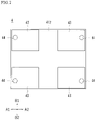
- FIG. 1 is a schematic configuration diagram schematically illustrating a configuration of a crystal oscillator according to an embodiment.
- FIG. 2 is a schematic plan view illustrating a first main surface of a first sealing member of the crystal oscillator.
- FIG. 3 is a schematic plan view illustrating a second main surface of the first sealing member of the crystal oscillator.
- FIG. 4 is a schematic plan view illustrating a first main surface of a crystal resonator plate of the crystal oscillator.
- FIG. 5 is a schematic plan view illustrating a second main surface of the crystal resonator plate of the crystal oscillator.
- FIG. 6 is a schematic plan view illustrating a first main surface of a second sealing member of the crystal oscillator.
- FIG. 7 is a schematic plan view illustrating a second main surface of the second sealing member of the crystal oscillator.
- FIG. 8 are diagrams respectively illustrating a state of the crystal resonator plate immediately after being subjected to an etching step of the crystal plate.
- FIG. 8 ( a ) is a schematic plan view of the first main surface while FIG. 8 ( b ) is a schematic plan view of the second main surface.
- FIG. 9 are enlarged diagrams each illustrating part of the crystal resonator plate in the vicinity of a connecting part that connects a support part to an external frame part.
- FIG. 9 ( a ) is a schematic plan view of a first main surface.
- FIGS. 9 ( b ) and 9 ( c ) are schematic cross-sectional views of the first main surface while FIG. 9 ( d ) is a schematic cross-sectional view of the second main surface.
- FIG. 10 is an enlarged diagram illustrating part of the crystal resonator plate in the vicinity of the connecting part that connects the support part to the external frame part, which schematically indicating respective shapes of an etching region and a lead-out wiring in plan view.
- FIG. 11 are enlarged diagrams each illustrating part of the crystal resonator plate in the vicinity of the connecting part that connects the support part to the external frame part.
- FIGS. 11 ( a ) and 11 ( b ) schematically indicate variations of the respective shapes of the etching region and the lead-out wiring in plan view.
- FIG. 12 are enlarged diagrams each illustrating part of the crystal resonator plate in the vicinity of the connecting part that connects the support part to the external frame part.
- FIGS. 12 ( a ) and 12 ( b ) schematically indicate variations of the respective shapes of the etching region and the lead-out wiring in plan view.
- FIG. 13 is an enlarged diagram illustrating part of the crystal resonator plate in the vicinity of the connecting part that connects the support part to the external frame part, which schematically indicating a variation of the respective shapes of the etching region and the lead-out wiring in plan view.
- FIG. 14 is an enlarged diagram illustrating part of the crystal resonator plate in the vicinity of the connecting part that connects the support part to the external frame part, which schematically indicating a shape of an entering part of the etching region in plan view.
- FIG. 15 are enlarged diagrams each illustrating part of the crystal resonator plate in the vicinity of the connecting part that connects the support part to the external frame part.
- FIGS. 15 ( a ) to 15 ( c ) indicate, in the crystal resonator plate whose etching region has the entering part, respective examples of a recess generated at a corner of the connecting part that connects the support part to the external frame part.
- FIG. 16 is an enlarged diagram illustrating part of the crystal resonator plate in the vicinity of the connecting part that connects the support part to the external frame part, which indicates a variation of a shape of the entering part.
- FIG. 17 are enlarged diagrams each illustrating part of the crystal resonator plate in the vicinity of the connecting part that connects the support part to the external frame part.
- FIGS. 17 ( a ) and 17 ( b ) each indicate a variation of the shape of the entering part.
- the present invention is applied to a crystal resonator device as a crystal oscillator.
- the crystal resonator device to which the present invention is applied is not limited to the crystal oscillator.
- the present invention may be applied to a crystal resonator.
- a crystal oscillator 101 includes: a crystal resonator plate 2 ; a first sealing member 3 ; a second sealing member 4 ; and an IC chip 5 .
- the crystal resonator plate 2 is bonded to the first sealing member 3 , and furthermore the crystal resonator plate 2 is bonded to the second sealing member 4 .
- a package 12 having a sandwich structure is formed so as to have a substantially rectangular parallelepiped shape.
- the IC chip 5 is mounted on a main surface of the first sealing member 3 so as to be opposed to a surface bonded to the crystal resonator plate 2 .
- the IC chip 5 as an electronic component element is a one-chip integrated circuit element constituting, with the crystal resonator plate 2 , an oscillation circuit.
- a first excitation electrode 221 is formed on a first main surface 211 as one main surface while a second excitation electrode 222 is formed on a second main surface 212 as the other main surface.
- the first sealing member 3 and the second sealing member 4 are bonded respectively to the main surfaces (the first main surface 211 and the second main surface 212 ) of the crystal resonator plate 2 , thus an internal space of the package 12 is formed.
- a vibrating part 22 (see FIGS. 4 and 5 ) including the first excitation electrode 221 and the second excitation electrode 222 is hermetically sealed.
- the crystal oscillator 101 has, for example, a package size of 1.0 ⁇ 0.8 mm, which is reduced in size and height. According to the size reduction, no castellation is formed in the package 12 . Through holes (described later) are used for conduction between electrodes.
- the crystal resonator plate 2 is a piezoelectric substrate made of crystal as shown in FIGS. 4 and 5 . Both main surfaces (i.e. the first main surface 211 and the second main surface 212 ) are formed as smooth flat surfaces (mirror-finished). In this embodiment, an AT-cut crystal plate that causes thickness shear vibration is used as the crystal resonator plate 2 . In the crystal resonator plate 2 shown in FIGS. 4 and 5 , each main surface 211 and 212 of the crystal resonator plate 2 is an XZ′ plane.
- the AT-cut method is a processing method in which a crystal plate is cut out of synthetic quartz crystal at an angle tilted by 35° 15′ about the X axis from the Z axis, out of the three crystal axes (i.e. an electrical axis (X axis), a mechanical axis (Y axis) and an optical axis (Z axis)) of the synthetic quartz crystal.
- the X axis of the AT-cut crystal plate equals the crystal axis of the crystal.
- the Y′ axis and the Z′ axis equal the respective axes that tilt by 35° 15′ from the Y axis and the Z axis out of the crystal axes of the crystal.
- the Y′ axis direction and the Z′ axis direction correspond to the directions in which the AT-cut crystal is cut out.
- a pair of excitation electrodes (i.e. the first excitation electrode 221 and the second excitation electrode 222 ) is formed, respectively, on the main surfaces 211 and 212 of the crystal resonator plate 2 .
- the crystal resonator plate 2 includes: the vibrating part 22 formed so as to have a substantially rectangular shape; an external frame part 23 surrounding the outer periphery of the vibrating part 22 ; and a support part 24 that supports the vibrating part 22 by connecting the vibrating part 22 to the external frame part 23 . That is, the crystal resonator plate 2 has a configuration in which the vibrating part 22 , the external frame part 23 and the support part 24 are integrally formed.
- the support part 24 is provided at only one position between the vibrating part 22 and the external frame part 23 .
- the vibrating part 22 and the support part 24 each have, basically, a thickness less than a thickness of the external frame part 23 . Due to the difference in thickness between the external frame part 23 and the support part 24 , the natural frequency of piezoelectric vibration differs between the external frame part 23 and the support part 24 . Thus, the external frame part 23 is not likely to resonate with the piezoelectric vibration of the support part 24 .
- the support part 24 is not necessarily formed at one part.
- the support part 24 may be formed at each of two parts between the vibrating part 22 and the external frame part 23 (for example, both sides in the ⁇ Z′ axis direction).
- the support part 24 extends (protrudes) from only one corner part positioned in the +X direction and in the ⁇ Z′ direction of the vibrating part 22 to the external frame part 23 in the ⁇ Z′ direction.
- the support part 24 is disposed on the corner part where displacement of the piezoelectric vibration is relatively small in an outer peripheral edge part of the vibrating part 22 , it is possible to prevent leakage of the piezoelectric vibration to the external frame part 23 via the support part 24 compared to the case in which the support part 24 is provided on the position other than the corner part (i.e. central part of the respective sides).
- the vibrating part 22 is piezoelectrically vibrated more effectively.
- the first excitation electrode 221 is provided on the first main surface 211 side of the vibrating part 22 while the second excitation electrode 222 is provided on the second main surface 212 side of the vibrating part 22 .
- the first excitation electrode 221 and the second excitation electrode 222 are respectively connected to lead-out wirings (a first lead-out wiring 223 and a second lead-out wiring 224 ) so that these excitation electrodes are connected to external electrode terminals.
- the first lead-out wiring 223 is drawn from the first excitation electrode 221 and connected to a connection bonding pattern 27 formed on the external frame part 23 via the support part 24 .
- the second lead-out wiring 224 is drawn from the second excitation electrode 222 and connected to a connection bonding pattern 28 formed on the external frame part 23 via the support part 24 .
- the first lead-out wiring 223 is formed on the first main surface 211 side of the support part 24 while the second lead-out wiring 224 is formed on the second main surface 212 side of the support part 24 .
- Resonator-plate-side sealing parts to bond the crystal resonator plate 2 respectively to the first sealing member 3 and the second sealing member 4 are provided on the respective main surfaces (i.e. the first main surface 211 and the second main surface 212 ) of the crystal resonator plate 2 .
- a resonator-plate-side first bonding pattern 251 is formed so as to be bonded to the first sealing member 3 .
- a resonator-plate-side second bonding pattern 252 is formed so as to be bonded to the second sealing member 4 .
- the resonator-plate-side first bonding pattern 251 and the resonator-plate-side second bonding pattern 252 are each formed on the external frame part 23 so as to have an annular shape in plan view.
- the first excitation electrode 221 and the second excitation electrode 222 are not electrically connected to the resonator-plate-side first bonding pattern 251 and the resonator-plate-side second bonding pattern 252 .
- five through holes are formed in the crystal resonator plate 2 so as to penetrate between the first main surface 211 and the second main surface 212 .
- four first through holes 261 are respectively disposed in the four corners (corner parts) of the external frame part 23 .
- a second through hole 262 is disposed in the external frame part 23 , on one side in the Z′ axis direction relative to the vibrating part 22 (in FIGS. 4 and 5 , on the side in the +Z′ direction).
- Connection bonding patterns 253 are formed on the respective peripheries of the first through holes 261 .
- a connection bonding pattern 254 is formed on the first main surface 211 side while the connection bonding pattern 28 is formed on the second main surface 212 side.
- first through holes 261 and the second through hole 262 through electrodes are respectively formed along a corresponding inner wall surface of the above through holes so as to establish conduction between the electrodes formed on the first main surface 211 and the second main surface 212 .
- Respective central parts of the first through holes 261 and the second through hole 262 are hollow through parts penetrating between the first main surface 211 and the second main surface 212 .
- the first excitation electrode 221 the second excitation electrode 222 ; the first lead-out wiring 223 ; the second lead-out wiring 224 , the first bonding pattern 251 ; the resonator-plate-side second bonding pattern 252 ; and the connection bonding patterns 253 , 254 , 27 and 28 .
- each of them can be formed by: a base film deposited on the main surface (the first main surface 211 or the second main surface 212 ) of the crystal resonator plate 2 by the physical vapor deposition; and a bonding film deposited on the base film by the physical vapor deposition.
- the base film is made of Ti (or Cr), and the bonding film is made of Au.
- the first sealing member 3 is a substrate having a rectangular parallelepiped shape that is made of a single glass wafer.
- a second main surface 312 (a surface to be bonded to the crystal resonator plate 2 ) of the first sealing member 3 is formed as a smooth flat surface (mirror finished).
- first main surface 311 the surface on which the IC chip 5 is mounted
- six electrode patterns 37 are formed, which include mounting pads for mounting the IC chip 5 as an oscillation circuit element.
- the IC chip 5 is bonded to the electrode patterns 37 by the flip chip bonding (FCB) method using a metal bump (for example, Au bump) 38 (see FIG. 1 ).
- FCB flip chip bonding
- FIGS. 2 and 3 six through holes are formed in the first sealing member 3 so as to be respectively connected to the six electrode patterns 37 and also to penetrate between the first main surface 311 and the second main surface 312 . More specifically, four third through holes 322 are respectively disposed in the four corners (corner parts) of the first sealing member 3 . Fourth and fifth through holes 323 and 324 are disposed respectively in the A 2 direction and in the A 1 direction in FIGS. 2 and 3 .
- the A 1 direction and the A 2 direction in FIGS. 2, 3, 6 and 7 respectively correspond to the ⁇ Z′ direction and the +Z′ direction in FIGS. 4 and 5
- the B 1 direction and B 2 direction in FIGS. 2, 3, 6 and 7 respectively correspond to the ⁇ X direction and the +X direction in FIGS. 4 and 5 .
- third through holes 322 and the fourth and fifth through holes 323 and 324 through electrodes are respectively formed along a corresponding inner wall surface of the above through holes so as to establish conduction between the electrodes formed on the first main surface 311 and the second main surface 312 .
- Respective central parts of the third through holes 322 and the fourth and fifth through holes 323 and 324 are hollow through parts penetrating between the first main surface 311 and the second main surface 312 .
- a sealing-member-side first bonding pattern 321 is formed as a sealing-member-side first sealing part so as to be bonded to the crystal resonator plate 2 .
- the sealing-member-side first bonding pattern 321 is formed so as to have an annular shape in plan view.
- connection bonding patterns 34 are respectively formed on the peripheries of the third through holes 322 .
- a connection bonding pattern 351 is formed on the periphery of the fourth through hole 323
- a connection bonding pattern 352 is formed on the periphery of the fifth through hole 324 .
- a connection bonding pattern 353 is formed on the side opposed to the connection bonding pattern 351 in the long axis direction of the first sealing member 3 (i.e. on the side of the A 2 direction).
- the connection bonding pattern 351 and the connection bonding pattern 353 are connected to each other via a wiring pattern 33 .
- the connection bonding pattern 353 is not connected to the connection bonding pattern 352 .
- the sealing-member-side first bonding pattern 321 it is possible to form the following elements by the same process: the sealing-member-side first bonding pattern 321 ; the connection bonding patterns 34 , and 351 to 353 ; and the wiring pattern 33 .
- each of them can be formed by: a base film deposited on the second main surface 312 of the first sealing member 3 by the physical vapor deposition; and a bonding film deposited on the base film by the physical vapor deposition.
- the base film is made of Ti (or Cr), and the bonding film is made of Au.
- the second sealing member 4 is a substrate having a rectangular parallelepiped shape that is made of a single glass wafer.
- a first main surface 411 (a surface to be bonded to the crystal resonator plate 2 ) of the second sealing member 4 is formed as a smooth flat surface (mirror finished).
- a sealing-member-side second bonding pattern 421 is formed as a sealing-member-side second sealing part so as to be bonded to the crystal resonator plate 2 .
- the sealing-member-side second bonding pattern 421 is formed so as to have an annular shape in plan view.
- External electrode terminals 43 which are electrically connected to the outside, are formed on a second main surface 412 (the outer main surface not facing the crystal resonator plate 2 ) of the second sealing member 4 .
- the external electrode terminals 43 are respectively located at four corner (corner parts) of the second sealing member 4 .
- each through hole is formed in the second sealing member 4 so as to penetrate between the first main surface 411 and the second main surface 412 .
- four sixth through holes 44 are respectively disposed in the four corners (corner parts) of the second sealing member 4 .
- through electrodes are respectively formed along a corresponding inner wall surface of the above through holes so as to establish conduction between the electrodes formed on the first main surface 411 and the second main surface 412 .
- Respective central parts of the sixth through holes 44 are hollow through parts penetrating between the first main surface 411 and the second main surface 412 .
- connection bonding patterns 45 are respectively formed on the peripheries of the sixth through holes 44 .
- the sealing-member-side second bonding pattern 421 it is possible to form the following elements by the same process: the sealing-member-side second bonding pattern 421 ; and the connection bonding patterns 45 .
- each of them can be formed by: a base film deposited on the first main surface 411 of the second sealing member 4 by the physical vapor deposition; and a bonding film deposited on the base film by the physical vapor deposition.
- the base film is made of Ti (or Cr), and the bonding film is made of Au.
- the crystal resonator plate 2 and the first sealing member 3 are subjected to the diffusion bonding in a state in which the resonator-plate-side first bonding pattern 251 and the sealing-member-side first bonding pattern 321 are superimposed on each other, and the crystal resonator plate 2 and the second sealing member 4 are subjected to the diffusion bonding in a state in which the resonator-plate-side second bonding pattern 252 and the sealing-member-side second bonding pattern 421 are superimposed on each other, thus, the package 12 having the sandwich structure shown in FIG. 1 is produced. Accordingly, the internal space of the package 12 , i.e. the space to house the vibrating part 22 is hermetically sealed.
- connection bonding patterns as described above are also subjected to the diffusion bonding in a state in which they are each superimposed on the corresponding connection bonding pattern.
- Such bonding between the connection bonding patterns allows electrical conduction of the first excitation electrode 221 , the second excitation electrode 222 , the IC chip 5 and the external electrode terminals 43 of the crystal oscillator 101 .
- the first excitation electrode 221 is connected to the IC chip 5 via the first lead-out wiring 223 , a bonding part between the connection bonding pattern 27 and the connection bonding pattern 353 , the wiring pattern 33 , the connection bonding pattern 351 , the through electrode in the fourth through hole 323 , and the electrode pattern 37 in this order.
- the second excitation electrode 222 is connected to the IC chip via the second lead-out wiring 224 , the connection bonding pattern 28 , the through electrode in the second through hole 262 , a bonding part between the connection bonding pattern 254 and the connection bonding pattern 352 , the through electrode in the fifth through hole 324 , and the electrode pattern 37 in this order.
- the IC chip 5 is connected to the external electrode terminals 43 via the electrode patterns 37 , the through electrodes in the third through holes 322 , bonding parts between the connection bonding patterns 34 and the connection bonding patterns 253 , the through electrodes in the first through holes 261 , bonding parts between the connection bonding patterns 253 and the connection bonding patterns 45 , and the through electrodes in the sixth through holes 44 in this order.
- a feature of the present invention is a relationship between the shape of a stepped part and the position of the lead-out wiring formed on the stepped part, in which the stepped part is generated by the difference in thickness between the external frame part 23 and the support part 24 of the crystal resonator plate 2 .
- this feature is described in detail.
- FIG. 8 are diagrams respectively illustrating a state of the crystal resonator plate 2 immediately after being subjected to an etching step of the crystal plate (i.e. a state before the electrodes and the wirings are formed).
- FIG. 8( a ) is a plan view of the first main surface 211 while FIG. 8 ( b ) is a plan view of the second main surface 212 .
- no mesa structure is formed on the center of the vibrating part.
- the rectangular-shaped crystal plate is subjected to the etching treatment two times, i.e. to the external shape forming etching and the frequency adjustment etching.
- a cut-out part is formed in the rectangular-shaped crystal plate so as to define respective external shapes of the vibrating part 22 , the external frame part 23 and the support part 24 .
- the through holes in the crystal resonator plate 2 are also formed in the external shape forming etching.
- the respective thicknesses of the vibrating part 22 and the support part 24 are adjusted so that the oscillating frequency of the crystal resonator device is a predetermined value.
- an etching region Eg made by the frequency adjustment etching is indicated by the hatched lines.
- the etching region Eg includes the vibrating part 22 and at least part of the support part 24 , and has a thickness thinner than the thickness of the external frame part 23 .
- a stepped part is formed due to the difference in thickness of the crystal plate.
- the stepped part has a cross-section perpendicular to the main surface of the crystal plate.
- the side surface of the stepped part is further inclined from the vertical state so as to have a caved shape in which the angle between the side surface of the stepped part and the main surface (i.e. the main surface of the support part or the main surface of the external frame part) is an acute angle.
- the lead-out wiring extended from the excitation electrode is formed over the stepped part having the vertical cross-section or the stepped part having the caved shape, disconnection of the lead-out wiring is likely to occur.
- the support part 24 extends (protrudes) from only one corner part positioned in the +X direction and in the ⁇ Z′ direction of the vibrating part 22 to the external frame part 23 in the ⁇ Z′ direction.
- the boundary between the support part 24 and the external frame part 23 is on the side parallel to the X axis out of the inner peripheral sides of the external frame part. Therefore, when the boundary of the etching region Eg is matched with the boundary between the support part 24 and the external frame part 23 (see FIG. 9 ( a ) ), the stepped part having the vertical cross-section (see FIG. 9 ( b ) ) or the stepped part having the caved shape (see FIG.
- the boundary of the etching region Eg on the first main surface 211 side is a stepped part having the vertical cross-section
- the boundary of the etching region Eg on the second main surface 212 side is a gentle stepped part (see FIG. 9 ( d ) ).
- the gentle shape means that the side surface of the stepped part is inclined so that the angle between the side surface of the stepped part and the main surface (i.e. the main surface of the support part or the main surface of the external frame part) is an obtuse angle.
- the crystal resonator plate 2 has a feature that the boundary shape of the etching region Eg is devised in order to prevent disconnection of the lead-out wiring extended from the excitation electrode.
- this sort of reflection is only required for one main surface of the crystal plate (here, the first main surface 211 ).
- the boundary of the etching region Eg may be matched with the boundary between the support part 24 and the external frame part 23 , as conventionally formed (see FIG. 8 ( b )).
- the boundary of the etching region Eg is not matched with the boundary between the support part 24 and the external frame part 23 .
- At least part of the boundary of the etching region Eg is a boundary line L 1 that is not parallel to the X axis, as shown in FIG. 10 .
- the stepped part generated at the boundary line L 1 is neither a stepped part having the vertical cross-section nor a stepped part having the caved shape, but is a gentle stepped part.
- the first lead-out wiring 223 on the first main surface 211 is formed so as to pass over at least part of the boundary line L 1 .
- the first lead-out wiring 223 is formed so as not to be parallel to the X axis in plan view.
- the first lead-out wiring 223 is formed on a gentle stepped part. Therefore, it is possible to sufficiently ensure the film thickness of the wiring on this part, which contributes to prevention of disconnection and increased resistance of the first lead-out wiring 223 .
- the shape of the boundary of the etching region Eg is not limited to the example indicated in FIG. 10 . Various other examples of the shape may be included. Some variations of the shape of the boundary of the etching region Eg are indicated in FIGS. 11 ( a ) , 11 ( b ), 12 ( a ), 12 ( b ) and 13 .
- the boundary of the etching region Eg includes not only the boundary line L 1 that is not parallel to the X axis, but also a boundary line L 2 that is parallel to the X axis.
- the entire etching region Eg may be the boundary line L 1 that is not parallel to the X axis.
- the boundary line L 1 that is not parallel to the X axis may have a curved shape (for example, an arc shape) in plan view as shown in FIG. 11 ( a ) , or may have a shape formed by a straight line in plan view as shown in FIGS. 11 ( b ) , 12 ( a ), 12 ( b ) and 13 .
- the boundary line L 1 as the straight line can form a further elongated gently stepped part.
- the boundary line L 1 is formed as a straight line
- the stepped part becomes gentler as the boundary line L 1 is formed so as to make an angle close to the right angle with the X axis in plan view, and the stepped part is the gentlest at the part where the boundary line L 1 makes the right angle with the X axis.
- the length W 1 of the straight line part is preferably half or more the width W 2 of the first lead-out wiring 223 (see FIG. 12 ( b ) ). Furthermore, when the straight line part is formed on the stepped part that is superimposed on the first lead-out wiring 223 , the length of the straight line part is more preferably not less than the width of the first lead-out wiring 223 (see FIGS. 11 ( b ) and 12 ( a )). That is, as the length of the straight line part is larger relative to the width of the first lead-out wiring 223 , disconnection or the like of the first lead-out wiring 223 can be further effectively reduced.
- the boundary of the etching region Eg (i.e. the stepped part) is formed on the external frame part 23 side relative to the boundary between the support part 24 and the external frame part 23 .
- the present invention is not limited thereto.
- the boundary of the etching region Eg may be formed on the support part 24 side relative to the boundary between the support part 24 and the external frame part 23 .
- the boundary of the stepped part in the +X direction is likely to have a cross-section with the caved shape.
- it is preferable that the boundary of the etching region Eg is formed on the external frame part 23 side.
- the etching region Eg has an entering part that is formed so as to enter part of the external frame part 23 .
- a start point P of the entering part on the ⁇ X side can be formed within a connection area R between the support part 24 and the external frame part 23 .
- the entering part is formed in the external frame part 23
- a recess is generated at the connecting part that connects the support part 24 to the external frame part 23 at the time of frequency adjustment etching under the condition that the start point P is formed on the extension line of the side of the support part 24 on the ⁇ X side.
- the recess acts as a stress concentration point at the connecting part that connects the support part 24 to the external frame part 23 , which leads to degradation of impact resistance of the crystal resonator device.
- the start point P is formed within the connection area R between the support part 24 and the external frame part 23 as shown in FIG. 10 , it is possible to avoid generation of the recess, which results in prevention of degradation of the impact resistance of the crystal resonator device.
- the entering part is formed in the etching region so as to enter the external frame part 23 from the support part 24 when the frequency adjustment etching is performed, in order to prevent disconnection of the first lead-out wiring 223 .
- the inventor of the present invention found that when the entering part is formed in the etching region, a recess may be formed at a corner of the connecting part that connects the support part 24 to the external frame part 23 during the frequency adjustment etching depending on the shape of the entering part, which may generate degradation of the impact resistance to the falling and the like.
- the main configuration of the crystal oscillator 101 according to the second embodiment is the same as the main configuration according to the first embodiment described with reference to FIGS. 1 to 7 . Therefore, the main configuration of the crystal oscillator 101 is omitted here.
- the feature of the second embodiment is related to the shape of the entering part that is formed in the external frame part 23 of the crystal resonator plate 2 at the time of the frequency adjustment etching. Hereinafter, this feature is described in detail.
- the crystal resonator plate 2 according to the second embodiment has a feature that the boundary shape of the etching region Eg is devised in order to prevent disconnection of the lead-out wiring extended from the excitation electrode and also to reduce degradation of the impact resistance of the connecting part that connects the external frame part 23 to the support part 24 .
- the boundary of the etching region Eg is not matched with the boundary between the support part 24 and the external frame part 23 , but the etching region Eg has an entering part Eg 1 that is formed so as to enter the external frame part 23 , as shown in FIG. 14 .
- the boundary of the entering part Eg 1 of the etching region Eg is a boundary line L 1 that is not parallel to the X axis.
- the stepped part generated at the boundary line L 1 is neither a stepped part having the vertical cross-section nor a stepped part having the caved shape, but is a gentle stepped part.
- the first lead-out wiring 223 on the first main surface 211 is formed so as to pass over at least part of the boundary line L 1 , which prevents disconnection or the like of the first lead-out wiring 223 .
- FIGS. 15 ( a ) to 15 ( c ) in the case in which a start point P 1 on the one side (in particular, the start point on the ⁇ X side) of the boundary of the entering part Eg 1 of the etching region is formed on an extension line L 3 of the side of the support part 24 on the ⁇ X side, it was found, by the inventor of the present invention, that a recess is generated at the connecting part that connects the support part 24 to the external frame part 23 at the time of frequency adjustment etching. Specifically, the recess is generated at a corner of the support part 24 on the ⁇ X side and on the ⁇ Z′ side. When such a recess is generated, the recess acts as a stress concentration point at the connecting part that connects the support part 24 to the external frame part 23 , which leads to degradation of impact resistance of the crystal resonator device.
- the start point P 1 of the boundary of the entering part Eg 1 of the etching region is formed at a position shifted from the extension line L 3 of the side of the support part 24 on the ⁇ X side. More specifically, the start point P 1 is shifted from the extension line L 3 toward the +X side so that the start point P 1 is formed within the connection area R between the support part 24 and the external frame part 23 .
- the start point P 1 is shifted from the extension line L 3 toward the +X side.
- the present invention is not limited thereto. That is, as shown in FIG. 16 , the start point P 1 may be shifted from the extension line L 3 toward the ⁇ X side. With such a configuration in which the start point P 1 is shifted from the extension line L 3 toward the ⁇ X side, it is also possible to avoid generation of the recess, which leads to prevention of degradation of the impact resistance of the crystal resonator device.
- the recess to be reduced in the present invention is generated only at a corner of the support part 24 on the ⁇ X side and on the ⁇ Z′ side due to the crystal anisotropy of the crystal plate.
- a start point P 2 on the other side (in particular, the start point on the +X side) of the boundary of the entering part Eg 1 may be formed on an extension line L 4 of the side of the support part 24 on the +X side, as shown in FIGS. 17 ( a ) and 17 ( b ).
- the entering part Eg 1 of the etching region Eg is formed only on one main surface (here, on the first main surface 211 ) of the crystal plate. In this case, it is possible to avoid unnecessary reduction of the plate thickness caused by forming the entering part Eg 1 , which leads to prevention of reduction of rigidity of the crystal resonator plate 2 .
Landscapes
- Physics & Mathematics (AREA)
- Acoustics & Sound (AREA)
- Engineering & Computer Science (AREA)
- Manufacturing & Machinery (AREA)
- Piezo-Electric Or Mechanical Vibrators, Or Delay Or Filter Circuits (AREA)
Abstract
Description
- 2 Crystal resonator plate
- 3 First sealing member
- 4 Second sealing member
- 205 IC chip
- 12 Package
- 22 Vibrating part
- 23 External frame part
- 24 Support part
- 101 Crystal oscillator (crystal resonator device)
- 211 First main surface
- 212 Second main surface
- 221 First excitation electrode
- 222 Second excitation electrode
- 223 First lead-out wiring
- 224 Second lead-out wiring
- Eg Etching region
- Eg1 Entering part
- P1 Start point of boundary line of entering part on −X side
- P2 Start point of boundary line of entering part on +X side
- L1 Boundary line not parallel to X axis
- L3 Extension line of side of support part on −X side
- L4 Extension line of side of support part on +X side
Claims (16)
Applications Claiming Priority (7)
| Application Number | Priority Date | Filing Date | Title |
|---|---|---|---|
| JP2017122550A JP6794938B2 (en) | 2017-06-22 | 2017-06-22 | Crystal diaphragm and crystal vibration device |
| JP2017-122550 | 2017-06-22 | ||
| JPJP2017-122550 | 2017-06-22 | ||
| JPJP2017-126147 | 2017-06-28 | ||
| JP2017126147A JP6794941B2 (en) | 2017-06-28 | 2017-06-28 | Crystal diaphragm and crystal vibration device |
| JP2017-126147 | 2017-06-28 | ||
| PCT/JP2018/021406 WO2018235582A1 (en) | 2017-06-22 | 2018-06-04 | Crystal diaphragm and crystal vibration device |
Publications (2)
| Publication Number | Publication Date |
|---|---|
| US20200144987A1 US20200144987A1 (en) | 2020-05-07 |
| US11411549B2 true US11411549B2 (en) | 2022-08-09 |
Family
ID=64737732
Family Applications (1)
| Application Number | Title | Priority Date | Filing Date |
|---|---|---|---|
| US16/618,113 Active 2039-07-27 US11411549B2 (en) | 2017-06-22 | 2018-06-04 | Crystal resonator plate and crystal resonator device |
Country Status (5)
| Country | Link |
|---|---|
| US (1) | US11411549B2 (en) |
| EP (1) | EP3644504B1 (en) |
| CN (1) | CN110463037B (en) |
| TW (1) | TWI660582B (en) |
| WO (1) | WO2018235582A1 (en) |
Families Citing this family (1)
| Publication number | Priority date | Publication date | Assignee | Title |
|---|---|---|---|---|
| WO2024024614A1 (en) * | 2022-07-28 | 2024-02-01 | 株式会社大真空 | Quartz crystal vibration plate and quartz crystal vibration device |
Citations (8)
| Publication number | Priority date | Publication date | Assignee | Title |
|---|---|---|---|---|
| US20130043960A1 (en) * | 2011-08-18 | 2013-02-21 | Seiko Epson Corporation | Resonating element, resonator, electronic device, electronic apparatus, moving vehicle, and method of manufacturing resonating element |
| US20130106247A1 (en) * | 2011-11-02 | 2013-05-02 | Nihon Dempa Kogyo Co., Ltd. | Piezoelectric vibrating piece and piezoelectric device |
| US20130193807A1 (en) * | 2012-01-31 | 2013-08-01 | Nihon Dempa Kogyo Co., Ltd. | Quartz crystal vibrating piece and quartz crystal device |
| US8541928B2 (en) * | 2011-03-23 | 2013-09-24 | Nihon Dempa Kogyo Co., Ltd. | Quartz-crystal devices exhibiting reduced crystal impedance |
| JP2014068098A (en) | 2012-09-25 | 2014-04-17 | Seiko Epson Corp | Vibration piece, vibration device, electronic apparatus and moving body |
| US20140203689A1 (en) * | 2013-01-18 | 2014-07-24 | Seiko Epson Corporation | Resonator element, resonator, oscillator, electronic apparatus and moving object |
| US20150035410A1 (en) * | 2013-08-05 | 2015-02-05 | Nihon Dempa Kogyo Co., Ltd. | Piezoelectric vibrating piece, method for fabricating the piezoelectric vibrating piece, piezoelectric device, and method for fabricating the piezoelectric device |
| WO2016121182A1 (en) | 2015-01-29 | 2016-08-04 | 株式会社大真空 | Crystal oscillation plate, and crystal oscillation device |
Family Cites Families (13)
| Publication number | Priority date | Publication date | Assignee | Title |
|---|---|---|---|---|
| JP3223949B2 (en) * | 1994-09-13 | 2001-10-29 | 株式会社大真空 | High frequency piezoelectric vibration device |
| JP3915117B2 (en) * | 2003-02-07 | 2007-05-16 | 株式会社大真空 | Piezoelectric vibration device |
| JP2008035383A (en) * | 2006-07-31 | 2008-02-14 | Epson Toyocom Corp | Piezoelectric device and method for manufacturing piezoelectric device |
| JP5446941B2 (en) * | 2010-01-29 | 2014-03-19 | 株式会社大真空 | Piezoelectric vibrating piece |
| JP5115598B2 (en) * | 2010-07-08 | 2013-01-09 | セイコーエプソン株式会社 | AT-cut crystal resonator element and crystal device |
| JP5624864B2 (en) * | 2010-12-06 | 2014-11-12 | 日本電波工業株式会社 | Temperature controlled crystal oscillator and crystal oscillator |
| CN202535316U (en) * | 2011-03-09 | 2012-11-14 | 精工爱普生株式会社 | Vibrating element, vibrator, oscillator and electronic equipment |
| TW201251157A (en) * | 2011-06-03 | 2012-12-16 | Seiko Epson Corp | Piezoelectric vibration element, manufacturing method for piezoelectric vibration element, piezoelectric vibrator, electronic device, and electronic apparatus |
| JP2013098777A (en) * | 2011-11-01 | 2013-05-20 | Nippon Dempa Kogyo Co Ltd | Crystal device |
| JP2013172244A (en) * | 2012-02-20 | 2013-09-02 | Nippon Dempa Kogyo Co Ltd | Method of manufacturing piezoelectric device and piezoelectric device |
| JP2014007538A (en) * | 2012-06-25 | 2014-01-16 | Daishinku Corp | Quartz vibration device |
| JP6275526B2 (en) * | 2014-03-28 | 2018-02-07 | 京セラ株式会社 | Piezoelectric vibrator, piezoelectric device, and method of manufacturing piezoelectric vibrator |
| CN107210725B (en) * | 2015-02-19 | 2020-06-02 | 株式会社村田制作所 | Crystal oscillator and crystal oscillator device |
-
2018
- 2018-06-04 US US16/618,113 patent/US11411549B2/en active Active
- 2018-06-04 EP EP18820823.5A patent/EP3644504B1/en active Active
- 2018-06-04 TW TW107119165A patent/TWI660582B/en active
- 2018-06-04 WO PCT/JP2018/021406 patent/WO2018235582A1/en not_active Ceased
- 2018-06-04 CN CN201880021121.0A patent/CN110463037B/en active Active
Patent Citations (9)
| Publication number | Priority date | Publication date | Assignee | Title |
|---|---|---|---|---|
| US8541928B2 (en) * | 2011-03-23 | 2013-09-24 | Nihon Dempa Kogyo Co., Ltd. | Quartz-crystal devices exhibiting reduced crystal impedance |
| US20130043960A1 (en) * | 2011-08-18 | 2013-02-21 | Seiko Epson Corporation | Resonating element, resonator, electronic device, electronic apparatus, moving vehicle, and method of manufacturing resonating element |
| US20130106247A1 (en) * | 2011-11-02 | 2013-05-02 | Nihon Dempa Kogyo Co., Ltd. | Piezoelectric vibrating piece and piezoelectric device |
| US20130193807A1 (en) * | 2012-01-31 | 2013-08-01 | Nihon Dempa Kogyo Co., Ltd. | Quartz crystal vibrating piece and quartz crystal device |
| JP2014068098A (en) | 2012-09-25 | 2014-04-17 | Seiko Epson Corp | Vibration piece, vibration device, electronic apparatus and moving body |
| US20140203689A1 (en) * | 2013-01-18 | 2014-07-24 | Seiko Epson Corporation | Resonator element, resonator, oscillator, electronic apparatus and moving object |
| US20150035410A1 (en) * | 2013-08-05 | 2015-02-05 | Nihon Dempa Kogyo Co., Ltd. | Piezoelectric vibrating piece, method for fabricating the piezoelectric vibrating piece, piezoelectric device, and method for fabricating the piezoelectric device |
| WO2016121182A1 (en) | 2015-01-29 | 2016-08-04 | 株式会社大真空 | Crystal oscillation plate, and crystal oscillation device |
| US20180006630A1 (en) * | 2015-01-29 | 2018-01-04 | Daishinku Corporation | Crystal resonator plate and crystal resonator device |
Also Published As
| Publication number | Publication date |
|---|---|
| WO2018235582A1 (en) | 2018-12-27 |
| TWI660582B (en) | 2019-05-21 |
| US20200144987A1 (en) | 2020-05-07 |
| EP3644504A4 (en) | 2020-06-10 |
| TW201906316A (en) | 2019-02-01 |
| EP3644504B1 (en) | 2023-02-15 |
| CN110463037A (en) | 2019-11-15 |
| EP3644504A1 (en) | 2020-04-29 |
| CN110463037B (en) | 2023-05-16 |
Similar Documents
| Publication | Publication Date | Title |
|---|---|---|
| US11342899B2 (en) | Crystal resonator device | |
| CN109804562B (en) | piezoelectric vibration device | |
| TWI668960B (en) | Piezo vibrating element and system integration package (SIP) module having the same | |
| US10771037B2 (en) | Piezoelectric resonator device | |
| US11824512B2 (en) | Piezoelectric resonator device | |
| JP6794941B2 (en) | Crystal diaphragm and crystal vibration device | |
| US11411549B2 (en) | Crystal resonator plate and crystal resonator device | |
| JP7056531B2 (en) | Crystal diaphragm and crystal vibration device | |
| TWI824438B (en) | Crystal oscillator and manufacturing method thereof | |
| US20260020499A1 (en) | Piezoelectric resonator device | |
| JP7172534B2 (en) | Piezoelectric oscillator manufacturing method | |
| JP6794938B2 (en) | Crystal diaphragm and crystal vibration device | |
| US12316301B2 (en) | Piezoelectric resonator plate and piezoelectric resonator device | |
| US20260031785A1 (en) | Crystal resonator plate and crystal resonator device | |
| JP2022184006A (en) | piezoelectric vibration device | |
| JP7725962B2 (en) | Crystal plate and crystal device | |
| TWI817286B (en) | Piezoelectric vibration device | |
| JP2019161458A (en) | Piezoelectric vibration device | |
| JP2025180897A (en) | Piezoelectric vibration device and method for manufacturing the same | |
| JP2023042422A (en) | Crystal oscillating plate and crystal oscillating device |
Legal Events
| Date | Code | Title | Description |
|---|---|---|---|
| FEPP | Fee payment procedure |
Free format text: ENTITY STATUS SET TO UNDISCOUNTED (ORIGINAL EVENT CODE: BIG.); ENTITY STATUS OF PATENT OWNER: LARGE ENTITY |
|
| AS | Assignment |
Owner name: DAISHINKU CORPORATION, JAPAN Free format text: ASSIGNMENT OF ASSIGNORS INTEREST;ASSIGNOR:YOSHIOKA, HIROKI;REEL/FRAME:051540/0074 Effective date: 20191015 |
|
| STPP | Information on status: patent application and granting procedure in general |
Free format text: APPLICATION DISPATCHED FROM PREEXAM, NOT YET DOCKETED |
|
| STPP | Information on status: patent application and granting procedure in general |
Free format text: DOCKETED NEW CASE - READY FOR EXAMINATION |
|
| STPP | Information on status: patent application and granting procedure in general |
Free format text: NON FINAL ACTION MAILED |
|
| STPP | Information on status: patent application and granting procedure in general |
Free format text: RESPONSE TO NON-FINAL OFFICE ACTION ENTERED AND FORWARDED TO EXAMINER |
|
| STPP | Information on status: patent application and granting procedure in general |
Free format text: NOTICE OF ALLOWANCE MAILED -- APPLICATION RECEIVED IN OFFICE OF PUBLICATIONS |
|
| STCF | Information on status: patent grant |
Free format text: PATENTED CASE |
|
| MAFP | Maintenance fee payment |
Free format text: PAYMENT OF MAINTENANCE FEE, 4TH YEAR, LARGE ENTITY (ORIGINAL EVENT CODE: M1551); ENTITY STATUS OF PATENT OWNER: LARGE ENTITY Year of fee payment: 4 |