US11409122B2 - Multilayer waveguide display element - Google Patents
Multilayer waveguide display element Download PDFInfo
- Publication number
- US11409122B2 US11409122B2 US16/954,952 US201816954952A US11409122B2 US 11409122 B2 US11409122 B2 US 11409122B2 US 201816954952 A US201816954952 A US 201816954952A US 11409122 B2 US11409122 B2 US 11409122B2
- Authority
- US
- United States
- Prior art keywords
- waveguide
- layers
- diffractive optical
- optical element
- layer
- Prior art date
- Legal status (The legal status is an assumption and is not a legal conclusion. Google has not performed a legal analysis and makes no representation as to the accuracy of the status listed.)
- Active, expires
Links
Images


Classifications
-
- G—PHYSICS
- G02—OPTICS
- G02B—OPTICAL ELEMENTS, SYSTEMS OR APPARATUS
- G02B27/00—Optical systems or apparatus not provided for by any of the groups G02B1/00 - G02B26/00, G02B30/00
- G02B27/01—Head-up displays
- G02B27/0101—Head-up displays characterised by optical features
-
- G—PHYSICS
- G02—OPTICS
- G02B—OPTICAL ELEMENTS, SYSTEMS OR APPARATUS
- G02B27/00—Optical systems or apparatus not provided for by any of the groups G02B1/00 - G02B26/00, G02B30/00
- G02B27/01—Head-up displays
- G02B27/017—Head mounted
- G02B27/0172—Head mounted characterised by optical features
-
- G—PHYSICS
- G02—OPTICS
- G02B—OPTICAL ELEMENTS, SYSTEMS OR APPARATUS
- G02B27/00—Optical systems or apparatus not provided for by any of the groups G02B1/00 - G02B26/00, G02B30/00
- G02B27/42—Diffraction optics, i.e. systems including a diffractive element being designed for providing a diffractive effect
- G02B27/4205—Diffraction optics, i.e. systems including a diffractive element being designed for providing a diffractive effect having a diffractive optical element [DOE] contributing to image formation, e.g. whereby modulation transfer function MTF or optical aberrations are relevant
-
- G—PHYSICS
- G02—OPTICS
- G02B—OPTICAL ELEMENTS, SYSTEMS OR APPARATUS
- G02B27/00—Optical systems or apparatus not provided for by any of the groups G02B1/00 - G02B26/00, G02B30/00
- G02B27/42—Diffraction optics, i.e. systems including a diffractive element being designed for providing a diffractive effect
- G02B27/4272—Diffraction optics, i.e. systems including a diffractive element being designed for providing a diffractive effect having plural diffractive elements positioned sequentially along the optical path
-
- G—PHYSICS
- G02—OPTICS
- G02B—OPTICAL ELEMENTS, SYSTEMS OR APPARATUS
- G02B5/00—Optical elements other than lenses
- G02B5/18—Diffraction gratings
- G02B5/1814—Diffraction gratings structurally combined with one or more further optical elements, e.g. lenses, mirrors, prisms or other diffraction gratings
- G02B5/1819—Plural gratings positioned on the same surface, e.g. array of gratings
-
- G—PHYSICS
- G02—OPTICS
- G02B—OPTICAL ELEMENTS, SYSTEMS OR APPARATUS
- G02B5/00—Optical elements other than lenses
- G02B5/18—Diffraction gratings
- G02B5/1828—Diffraction gratings having means for producing variable diffraction
-
- G—PHYSICS
- G02—OPTICS
- G02B—OPTICAL ELEMENTS, SYSTEMS OR APPARATUS
- G02B6/00—Light guides; Structural details of arrangements comprising light guides and other optical elements, e.g. couplings
Definitions
- the invention relates to diffractive waveguide display elements, which can be used in personal display devices, such as head-mounted displays (HMDs) and head-up displays (HUDs).
- HMDs head-mounted displays
- HUDs head-up displays
- Diffractive waveguide elements typically comprise a single waveguide layer or a plurality of stacked layers. In the case of several layers, different colors or different parts of the field-of-view of the image to be displayed can be guided in different layers. In that case, each of the layers comprises a separate in-coupling grating for coupling part of the image to the layer, and a separate out-coupling grating for coupling the part of the image out of the element.
- the invention is based on providing a multilayer waveguide in which there is one or more gratings or other diffractive optical element between the layers for redistributing the light power between the layers while the light propagates in the waveguide.
- the ratio of light power between the layers is different from another lateral point along the propagation path of light. This is in contrast with prior solutions in which the once in-coupled light remains in the same layer until out-coupled therefrom.
- the invention provides waveguide display element for guiding an image from a first lateral zone of the element to a second lateral zone of the element, the element comprising a plurality of waveguide layers on top of each other.
- the element further comprises at least one intermediate diffractive optical element arranged between two of said waveguide layers.
- the intermediate diffractive optical element is adapted to change the distribution of propagating light power between the layers.
- the invention offers significant benefits. Most importantly, the invention provides new freedoms of design. Light which is once coupled to propagate in one layer need not stay there until out-coupled, but can be moved to a neighboring layer one or more times. This allows for implementing completely new display products.
- the out-coupling modulation can be implemented by the one or more intermediate DOEs instead of direct modulation of the out-coupling grating.
- the intermediate DOEs can be used to make the light to “climb” the stairs. Between the stairs, more layers can be used for light propagation and/or in/out-coupling and at the region of the discrete stairs the light is packed to a lesser number of layers or to one layer only. Alternatively, or in addition to that, a targeted transition from one layer to another can be made exactly at the location of a stair. Staircase profile is beneficial for example when implementing waveguides with a definite focus plane.
- the invention can be used to assist in multiplication of laser beams so as to provide a denser field of beams at the out-coupling, for preventing striping of the image as seen by the user.
- the invention can be used in narrow-wavelength waveguides, such as laser-illuminated waveguides, but is applicable also in wideband applications.
- the invention concerns changing the power distribution of propagating light. That is, for example light coupled out of the waveguide and passing through an intermediate layer without propagating therein—or that is not intended to propagate to a significant degree therein—is not in the focus of the invention and does not change the power distribution in the present sense.
- the diffractive optical response of the at least one intermediate DOE may be non-constant or constant within the area of the element.
- a constant element one can achieve a laterally constant shift of light power from one layer to another.
- a non-constant element a localized shift of power or a laterally varying power shift distribution can be achieved, for example.
- Local power redistribution offers new possibilities, some of which are exemplified herein in detail.
- the element comprises an out-coupling DOE on a first of said layers at said second lateral zone
- the intermediate DOE is adapted to pass light power from a second layer adjacent to said first layer to the first layer depending on the position within said second zone so as to control the distribution of light out-coupled from the waveguide.
- the waveguide has a staircase profile comprising at least one discrete step in the propagation path of light from said first zone to said second zone, and the intermediate DOE is adapted to control the distribution of light between said layers for assisting the propagating light power to pass the step.
- at least one of the layers of the waveguide element continues over the step as a continuous layer, and the intermediate DOE is adapted to increase light power in the continuous layer before the step for assisting light to “climb the stair”.
- the element comprises a plurality of in-coupling diffractive optical elements at said first lateral zone, the in-coupling diffractive optical elements being associated with said layers for coupling initial light power into the layers.
- the intermediate DOE is provided between waveguide layers having different thicknesses, so that the amount of rays, directed to thinner of the layers is multiplied and coupled by the intermediate optical element to the thicker of the layers. This has particular relevance in the case of coherent narrow-beam laser illumination.
- the intermediate DOE covers the zone of the element from the first lateral zone (image in-coupling zone) to the second lateral zone (image out-coupling zone).
- the DOE typically has a non-constant diffractive optical response so that the coupling efficiency is higher at one location thereof than at another location thereof.
- the waveguide element comprises at least three waveguide layers and at least two such intermediate diffractive optical elements between pairs of waveguide layers.
- the waveguide layers can be stacked layers, each intermediate DOE being manufactured onto one of the waveguide layers before stacking.
- the waveguide layers can also be formed of a unitary piece of light-guiding material being partitioned by fabricating said intermediate diffractive optical element.
- the intermediate DOE between any two waveguide layers provides a spatially continuous optical interaction between the layers, there typically being continuous light transfer in both directions and the net flow of light power being towards one of the layers at least at some location of the DOE.
- FIGS. 1-5 show a cross-sectional side views of exemplary multilayer waveguides according to the invention.
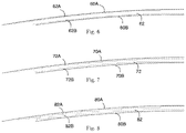
- FIGS. 6-8 illustrate in cross-sectional views different variations of waveguide elements having staircase surface profiles.
- DOE diffractive optical element
- the term “diffractive optical element” refers to a zone of the waveguide body comprising a physical structure capable of diffracting light.
- the structure typically comprises a pattern of features having a size of 1 ⁇ m or less.
- the DOE may be either periodic or non-periodic and have a constant (single-region) or non-constant diffractive optical response over its area.
- a non-constant diffractive optical response DOE may be a multi-region DOE.
- intermediate DOE refers to a DOE that is not intended to out-couple light directly therefrom, but to change the propagation path of light rays from one layer to another. Due to imperfections, a certain amount of out-coupling may, however occur. Typically, at least 90% of propagating light hitting the intermediate DOE continues propagation in either the original layer or the new layer, depending on the predefined optical response.
- DOE diffractive optical response of the DOE refers to the change in the angular and/or spectral distribution of light by the DOE due to diffraction. To concretize, the response may be e.g. diffraction intensity to a specific angle for a fixed incident angle and wavelength. A diffractive microstructure pattern of the DOE generates the diffractive optical response.
- Multi-region DOE refers to a DOE that has several internal regions with different diffractive optical response. In some designs, the regions have a real area and the diffractive optical response within those regions is constant. The smooth changing of the diffractive optical response takes place between the regions. In alternative designs, the regions are infinitesimally small, whereby the smooth changing takes place essentially throughout the DOE. Also combinations of these designs are possible.
- “Staircase profile” means a surface profile with a plurality of discrete (abrupt) height changes.
- the profile has a plurality of distinguishable sub-surfaces at an angle with respect to neighboring sub-surfaces in at least one cross-sectional plane, thus forming a plurality of steps resembling the form of a staircase.
- every second sub-surface can be parallel or approximately parallel with is neighboring every second sub-surface.
- the dimensions of the steps in the general plane of the waveguide by are larger than the optical diffractive limit so that the profile itself does not cause significant diffraction of light but rather guide the light according to a desired geometric scheme with high efficiency.
- the layered waveguides discussed herein can be used to control the power distribution inside the waveguide.
- This can be utilized e.g. in augmented reality (AR) applications by for example designing the system so that most of the light propagates in a central part of the waveguide in at least some section thereof. Thereby it is not exposed to out-coupling gratings on the waveguide surface, which means that the overall power distribution does not have to be considered in detail at these gratings, but can instead be handled by selecting the inter-waveguide gratings appropriately.
- Such decoupling of the optical functions of the waveguide leads to a greater number of design freedoms, which translates into improved performance.
- FIG. 1 shows a multi-layer waveguide comprising three layers 10 A, 10 B, 10 C.
- Each layer comprises an in-coupling grating 12 A, 12 B, 12 C that couples incoming light beams 11 A, 11 B, 11 C, respectively, to the layers 10 A, 10 B, 10 C to propagate therein as propagating waves 13 A, 13 B, 13 C (herein shown as arrows showing the net propagation direction, although in reality bouncing between waveguide surfaces and/or limiting DOEs is seen).
- intermediate diffractive optical elements 14 AB, 14 BC that are configured, at predefined locations thereof, to couple light from one layer to another.
- light is transferred from the middle layer 10 B to the topmost layer 10 A as net flow 15 BA and from the bottom layer 10 C to the middle layer as net flow 15 CB.
- Light continues to propagate in the new layer until again coupled to another layer.
- the distribution of light between the layers is different depending on the location.
- the out-coupling distribution depends on the “feeding” of the topmost layer 10 A by the underlying layers 10 B, 10 C.
- DOEs herein discussed are non-binary and/or the indices of refraction of the waveguides between which the DOEs are located are different.
- the arrows across DOEs illustrate the net flow.
- FIG. 2 shows an embodiment, where there is two-way net flow of light.
- propagating light is transferred from the top layer 10 A and the middle layer 10 B to the bottom layer 10 C.
- all rays are transferred first to the middle layer 10 B to the top layer 10 A and further out of the waveguide.
- FIG. 3 illustrates controlling the out-coupling efficiency of the waveguide using the intermediate diffractive optical element.
- the waveguide comprises a top layer 30 A and bottom layer 30 B. All incoming light 31 B is at first coupled to the bottom layer 30 B, where it propagates laterally via total internal reflections as light field 33 B. Aligned with the out-coupling grating 36 on top of the top layer 30 A, there is an intermediate DOE 34 AB. The intermediate DOE 34 AB transfers selectively light from the bottom layer 30 B to the top layer 30 A, with coupling efficiency depending on the location. At a first location, a net flow 35 BA is seen, at another location, there is net flow 35 BA′ and at a third location, there is net flow 35 BA′′. These net flows determine the spatial distribution of light power at the top layer 30 A, that interacts with the out-coupling grating 36 . Therefore, different intensities of out-coupled light beams 37 B, 37 B′, 37 B′′ are seen, depending on the location.
- a benefit of the arrangement of FIG. 3 is that as light is coupled to the bottom layer 30 B, leakage in in-coupled light back through the in-coupling grating 31 B can be prevented to high degree or even entirely.
- the out-coupling grating 36 is a non-modulated grating, i.e. has a constant coupling efficiency over its area.
- the out-coupling efficiency is entirely regulated by the properties of the underlying intermediate diffractive optical element, which may be a modulated grating or have a more complex diffractive response.
- the intermediate DOE is adapted to pass a non-even light power distribution from one layer to another. This can be achieved using a multi-region DOE, an efficiency-modulated grating or the like.
- Staircase waveguides comprise a specific waveguide structure where the ability to control the power distribution is an essential improvement. Indeed, in these structures light has to pass from one stacked waveguide to another with as little lost light as possible, and one potential solution to this problem is provided by a waveguide layer common to both stacked waveguides.
- FIGS. 6-8 show examples of staircase waveguides.
- a staircase waveguide is a diffractive waveguide element which comprises a waveguide region 62 , 72 , 82 defined by two optical surfaces 62 A, 62 B; 72 A, 72 B; 82 A, 82 B, at least one of which has a staircase profile, and between which light can propagate by total internal reflections, the optical surfaces having surface profiles, and at least one diffractive optical element, in particular a grating, capable of modifying the light field within the waveguide region.
- FIGS. 6-8 illustrate that different step-sizes of the waveguide region can be used to produce staircase waveguides that follow the same outer surface shape.
- the outer surface 60 A, 60 B; 70 A, 70 B, 80 A, 80 B may be physically explicitly present or imaginary.
- the staircase surfaces 62 A, 62 B; 72 A, 72 B; 82 A, 82 B, or a surface-conformant coating thereon typically form the outer surface of the waveguide.
- the first and second surface profiles have stairs (intermediate surfaces) aligned with each other in the horizontal direction.
- the stair height in FIG. 6 is smaller than in FIG. 7 .
- the stairs in the first and second surfaces 82 A, 82 B are interleaved, i.e. non-aligned with each other.
- the resulting waveguide 82 implements the same general waveguide shape as the waveguides 62 , 72 of FIGS. 6 and 7 .
- FIG. 4 shows one possible implementation of the inner structure of a waveguide region of a staircase waveguide. Instead of a single waveguide layer only, it comprises a plurality of layers 40 A-E at least one of which continues as unbroken over the stair. On each side of the stair, there are several layers, herein three layers 40 A, 40 B, 40 C/ 40 A, 40 D, 40 E, respectively. Light is initially coupled to a plurality of first side layers 40 A, 40 B, 40 C. Upstream of the stair, there is provide at least one DOE 44 AB, 44 BC, which is adapted to change the power distribution of light between the layers 40 A, 40 B, 40 C so that light is “packed” to the continuous layer 40 A before the stair.
- DOE 44 AB, 44 BC Upstream of the stair, there is provide at least one DOE 44 AB, 44 BC, which is adapted to change the power distribution of light between the layers 40 A, 40 B, 40 C so that light is “packed” to the continuous layer 40 A before the stair.
- FIG. 5 shows an embodiment, where a ray multiplier layer 50 A is provided on another waveguide layer 50 B.
- the multiplier layer 50 A comprises a waveguide which is thinner and smaller in area than the main waveguide layer 50 B.
- the intermediate DOE 52 herein also serving as the in-coupling grating, is provided between the multiplier layer 50 A and the main waveguide 50 B.
- the incident ray 51 B bounces in the multiplier layer 50 A with short bounce period, and at each bounce at the in-coupling grating 52 , part of light is diffracted into the display waveguide 50 B.
- the ray is multiplied and a denser field of light rays exits the main waveguide 50 B at the out-coupling grating 56 .
- This provides significant benefits in particular in the case of laser-illuminated waveguides, in which striping of the image due to sparse out-coupled ray fields is a problem.
- the intermediate DOE or DOEs may adapted to change the distribution of light power between the layers depending on the wavelength and/or angle of incidence.
- the main propagation direction of light in each layer is the same, but this does not need to be the case. It is possible for example that the direction of net flow of light in different layers is the opposite, or there may be any oblique angle between the new flow directions.
- a spherical waveguide for example, comprises two concentric spherical surfaces (the principal surfaces of the waveguide) between which the rays of the light-field bounce.
- Embodiments of the invention can be utilized in various personal display devices, augmented reality (AR), virtual reality (VR) and mixed reality (MR) devices, like near-to-the-eye displays (NEDs) and other head-mounted displays (HMDs), as well as head-up displays (HUDs), in their different forms.
- AR augmented reality
- VR virtual reality
- MR mixed reality
- NEDs near-to-the-eye displays
- HMDs head-mounted displays
- HUDs head-up displays
- the waveguide or individual layers thereof may comprise, in addition to the intermediate DOE(s) and in-coupling and out-coupling gratings, also other diffractive optical elements, such as exit pupil expander gratings or beam redirection gratings.
Landscapes
- Physics & Mathematics (AREA)
- General Physics & Mathematics (AREA)
- Optics & Photonics (AREA)
- Optical Couplings Of Light Guides (AREA)
- Diffracting Gratings Or Hologram Optical Elements (AREA)
- Optical Integrated Circuits (AREA)
Applications Claiming Priority (3)
| Application Number | Priority Date | Filing Date | Title |
|---|---|---|---|
| FI20176156 | 2017-12-22 | ||
| FI20176156A FI128028B (en) | 2017-12-22 | 2017-12-22 | Monikerrosaaltojohdenäyttöelementti |
| PCT/FI2018/050958 WO2019122528A1 (en) | 2017-12-22 | 2018-12-20 | Multilayer waveguide display element |
Publications (2)
| Publication Number | Publication Date |
|---|---|
| US20200333614A1 US20200333614A1 (en) | 2020-10-22 |
| US11409122B2 true US11409122B2 (en) | 2022-08-09 |
Family
ID=66994451
Family Applications (1)
| Application Number | Title | Priority Date | Filing Date |
|---|---|---|---|
| US16/954,952 Active 2039-08-06 US11409122B2 (en) | 2017-12-22 | 2018-12-20 | Multilayer waveguide display element |
Country Status (7)
| Country | Link |
|---|---|
| US (1) | US11409122B2 (de) |
| EP (1) | EP3710874B1 (de) |
| JP (1) | JP7308205B2 (de) |
| KR (1) | KR102651487B1 (de) |
| CN (1) | CN111492273B (de) |
| FI (1) | FI128028B (de) |
| WO (1) | WO2019122528A1 (de) |
Cited By (3)
| Publication number | Priority date | Publication date | Assignee | Title |
|---|---|---|---|---|
| US20220283371A1 (en) * | 2019-02-14 | 2022-09-08 | Magic Leap, Inc. | Method and system for variable optical thickness waveguides for augmented reality devices |
| US11860416B2 (en) | 2019-02-14 | 2024-01-02 | Magic Leap, Inc. | Biased total thickness variations in waveguide display substrates |
| US20240337845A1 (en) * | 2023-04-07 | 2024-10-10 | Aac Optics (Changzhou) Co., Ltd. | Optical waveguide lens and near-eye display device |
Families Citing this family (9)
| Publication number | Priority date | Publication date | Assignee | Title |
|---|---|---|---|---|
| FI128594B (en) * | 2017-12-22 | 2020-08-31 | Dispelix Oy | Stair waveguide elements, personal display device and method for producing an image |
| FI128573B (en) * | 2018-03-28 | 2020-08-14 | Dispelix Oy | Waveguide display element |
| TWI718054B (zh) | 2020-04-23 | 2021-02-01 | 宏碁股份有限公司 | 結合眼鏡功能與擴增實境功能的光學裝置及擴增實境裝置 |
| CN113703173B (zh) * | 2020-05-20 | 2023-08-15 | 宏碁股份有限公司 | 结合眼镜功能与扩增实境功能的光学装置及扩增实境装置 |
| US11650372B2 (en) | 2020-09-21 | 2023-05-16 | Corning Incorporated | Optical coupling device having diffraction gratings for coupling light with a light guide and fabrication method thereof |
| EP4130848B1 (de) * | 2021-08-02 | 2024-05-08 | Nokia Technologies Oy | Optische vorrichtung, head-up display und entsprechendes verfahren |
| US11962351B2 (en) * | 2021-12-01 | 2024-04-16 | X Development Llc | Multilayer photonic devices with metastructured layers |
| US12546929B2 (en) | 2022-02-15 | 2026-02-10 | Boe Technology Group Co., Ltd. | Optical waveguide structure and display device |
| KR102759532B1 (ko) | 2022-05-19 | 2025-01-23 | 김은석 | 스마트 글래스 |
Citations (21)
| Publication number | Priority date | Publication date | Assignee | Title |
|---|---|---|---|---|
| US20060126179A1 (en) | 2004-12-13 | 2006-06-15 | Nokia Corporation | Method and system for beam expansion in a display device |
| US20100246003A1 (en) | 2007-12-18 | 2010-09-30 | Bae Systems Plc | projection displays |
| US20110026128A1 (en) | 2008-04-14 | 2011-02-03 | Bae Systems Plc | waveguides |
| EP2733517A1 (de) | 2012-11-16 | 2014-05-21 | Rockwell Collins, Inc. | Transparentes Wellenleiteranzeigegerät |
| US9134535B2 (en) * | 2010-09-17 | 2015-09-15 | Carl Zeiss Ag | Display device having a holding device that can be placed on the head of a user |
| WO2017003674A1 (en) * | 2015-06-30 | 2017-01-05 | Microsoft Technology Licensing, Llc | Diffractive optical elements with graded edges |
| US20170045745A1 (en) * | 2014-07-11 | 2017-02-16 | Samsung Electronics Co., Ltd. | Lightguide structure, optical device and imaging system |
| US20170059879A1 (en) * | 2015-08-27 | 2017-03-02 | Tuomas Vallius | Diffractive optical element using polarization rotation grating for in-coupling |
| CN106526730A (zh) | 2016-11-21 | 2017-03-22 | 苏州苏大维格光电科技股份有限公司 | 一种宽视角波导镜片及制作方法和头戴式三维显示装置 |
| US20170123208A1 (en) | 2015-10-29 | 2017-05-04 | Tuomas Vallius | Diffractive optical element with uncoupled grating structures |
| US20170131546A1 (en) | 2015-11-10 | 2017-05-11 | Scott Woltman | Waveguide gratings to improve intensity distributions |
| US20170139110A1 (en) | 2012-05-18 | 2017-05-18 | Reald Spark, Llc | Directionally illuminated waveguide arrangement |
| WO2017120320A1 (en) | 2016-01-06 | 2017-07-13 | Vuzix Corporation | Two channel imaging light guide with dichroic reflectors |
| US20170235144A1 (en) | 2014-07-15 | 2017-08-17 | Samsung Electronics Co., Ltd. | Holographic see-through optical device, stereoscopic imaging system, and multimedia head mounted system |
| US20170257089A1 (en) | 2016-03-01 | 2017-09-07 | Kuka Roboter Gmbh | Electrical Device With A Pulsed Power Supply And Method For Examining The Power Supply Of The Electrical Device |
| DE102016109288A1 (de) | 2016-05-20 | 2017-11-23 | Carl Zeiss Smart Optics Gmbh | Brillenglas für eine Abbildungsoptik und Datenbrille |
| US20170357089A1 (en) * | 2016-06-09 | 2017-12-14 | Microsoft Technology Licensing, Llc | Wrapped Waveguide With Large Field Of View |
| US20170363870A1 (en) * | 2016-06-17 | 2017-12-21 | Google Inc. | Method for fabricating a curved eyepiece |
| US20180196275A1 (en) * | 2017-01-04 | 2018-07-12 | Reald Spark, Llc | Optical stack for imaging directional backlights |
| US20210063638A1 (en) * | 2017-12-29 | 2021-03-04 | Universiteit Gent | Temperature insensitive filter |
| US11281010B2 (en) * | 2017-12-22 | 2022-03-22 | Dispelix Oy | Curved staircase waveguide element, personal display device and method of producing an image |
Family Cites Families (9)
| Publication number | Priority date | Publication date | Assignee | Title |
|---|---|---|---|---|
| JPH0618727A (ja) * | 1992-06-29 | 1994-01-28 | Sharp Corp | 照明装置 |
| EP1922579B1 (de) * | 2005-09-07 | 2015-08-19 | BAE Systems PLC | Projektionsanzeige mit zwei plattenartigen coplanaren, gitter enthaltenden wellenleitern |
| EP2196729A1 (de) * | 2008-12-12 | 2010-06-16 | BAE Systems PLC | Verbesserungen an oder im Zusammenhang mit Wellenleitern |
| US9188731B2 (en) * | 2012-05-18 | 2015-11-17 | Reald Inc. | Directional backlight |
| US8913324B2 (en) * | 2012-08-07 | 2014-12-16 | Nokia Corporation | Display illumination light guide |
| CN104536136A (zh) * | 2015-01-25 | 2015-04-22 | 上海理湃光晶技术有限公司 | 一种用于显示的折叠准直光学波导器件 |
| CN104656259B (zh) * | 2015-02-05 | 2017-04-05 | 上海理湃光晶技术有限公司 | 共轭窄带三基色交错的体全息光栅波导近眼光学显示器件 |
| US9864208B2 (en) * | 2015-07-30 | 2018-01-09 | Microsoft Technology Licensing, Llc | Diffractive optical elements with varying direction for depth modulation |
| DE102015122055B4 (de) * | 2015-12-17 | 2018-08-30 | Carl Zeiss Ag | Optisches System sowie Verfahren zum Übertragen eines Quellbildes |
-
2017
- 2017-12-22 FI FI20176156A patent/FI128028B/en active IP Right Grant
-
2018
- 2018-12-20 EP EP18893292.5A patent/EP3710874B1/de active Active
- 2018-12-20 JP JP2020533831A patent/JP7308205B2/ja active Active
- 2018-12-20 WO PCT/FI2018/050958 patent/WO2019122528A1/en not_active Ceased
- 2018-12-20 KR KR1020207019831A patent/KR102651487B1/ko active Active
- 2018-12-20 US US16/954,952 patent/US11409122B2/en active Active
- 2018-12-20 CN CN201880081674.5A patent/CN111492273B/zh active Active
Patent Citations (22)
| Publication number | Priority date | Publication date | Assignee | Title |
|---|---|---|---|---|
| US20060126179A1 (en) | 2004-12-13 | 2006-06-15 | Nokia Corporation | Method and system for beam expansion in a display device |
| US20100246003A1 (en) | 2007-12-18 | 2010-09-30 | Bae Systems Plc | projection displays |
| US20110026128A1 (en) | 2008-04-14 | 2011-02-03 | Bae Systems Plc | waveguides |
| US9134535B2 (en) * | 2010-09-17 | 2015-09-15 | Carl Zeiss Ag | Display device having a holding device that can be placed on the head of a user |
| US20170139110A1 (en) | 2012-05-18 | 2017-05-18 | Reald Spark, Llc | Directionally illuminated waveguide arrangement |
| EP2733517A1 (de) | 2012-11-16 | 2014-05-21 | Rockwell Collins, Inc. | Transparentes Wellenleiteranzeigegerät |
| US20170045745A1 (en) * | 2014-07-11 | 2017-02-16 | Samsung Electronics Co., Ltd. | Lightguide structure, optical device and imaging system |
| US20170235144A1 (en) | 2014-07-15 | 2017-08-17 | Samsung Electronics Co., Ltd. | Holographic see-through optical device, stereoscopic imaging system, and multimedia head mounted system |
| WO2017003674A1 (en) * | 2015-06-30 | 2017-01-05 | Microsoft Technology Licensing, Llc | Diffractive optical elements with graded edges |
| US20170059879A1 (en) * | 2015-08-27 | 2017-03-02 | Tuomas Vallius | Diffractive optical element using polarization rotation grating for in-coupling |
| US20170123208A1 (en) | 2015-10-29 | 2017-05-04 | Tuomas Vallius | Diffractive optical element with uncoupled grating structures |
| US20170131546A1 (en) | 2015-11-10 | 2017-05-11 | Scott Woltman | Waveguide gratings to improve intensity distributions |
| WO2017120320A1 (en) | 2016-01-06 | 2017-07-13 | Vuzix Corporation | Two channel imaging light guide with dichroic reflectors |
| US20170257089A1 (en) | 2016-03-01 | 2017-09-07 | Kuka Roboter Gmbh | Electrical Device With A Pulsed Power Supply And Method For Examining The Power Supply Of The Electrical Device |
| DE102016109288A1 (de) | 2016-05-20 | 2017-11-23 | Carl Zeiss Smart Optics Gmbh | Brillenglas für eine Abbildungsoptik und Datenbrille |
| US11054651B2 (en) * | 2016-05-20 | 2021-07-06 | tooz technologies GmbH | Spectacle lens for an imaging optical unit and data goggles |
| US20170357089A1 (en) * | 2016-06-09 | 2017-12-14 | Microsoft Technology Licensing, Llc | Wrapped Waveguide With Large Field Of View |
| US20170363870A1 (en) * | 2016-06-17 | 2017-12-21 | Google Inc. | Method for fabricating a curved eyepiece |
| CN106526730A (zh) | 2016-11-21 | 2017-03-22 | 苏州苏大维格光电科技股份有限公司 | 一种宽视角波导镜片及制作方法和头戴式三维显示装置 |
| US20180196275A1 (en) * | 2017-01-04 | 2018-07-12 | Reald Spark, Llc | Optical stack for imaging directional backlights |
| US11281010B2 (en) * | 2017-12-22 | 2022-03-22 | Dispelix Oy | Curved staircase waveguide element, personal display device and method of producing an image |
| US20210063638A1 (en) * | 2017-12-29 | 2021-03-04 | Universiteit Gent | Temperature insensitive filter |
Non-Patent Citations (3)
| Title |
|---|
| Chinese Office Action dated Aug. 3, 2021 as received in application No. 201880081674.5. |
| European Search Report dated Jul. 20, 2021 as received in application No. 18893292. |
| Finnish Office Action dated Jun. 15, 2018 as received in application No. 20176156. |
Cited By (5)
| Publication number | Priority date | Publication date | Assignee | Title |
|---|---|---|---|---|
| US20220283371A1 (en) * | 2019-02-14 | 2022-09-08 | Magic Leap, Inc. | Method and system for variable optical thickness waveguides for augmented reality devices |
| US11860416B2 (en) | 2019-02-14 | 2024-01-02 | Magic Leap, Inc. | Biased total thickness variations in waveguide display substrates |
| US12332481B2 (en) | 2019-02-14 | 2025-06-17 | Magic Leap, Inc. | Biased total thickness variations in waveguide display substrates |
| US12399320B2 (en) * | 2019-02-14 | 2025-08-26 | Magic Leap, Inc. | Method and system for variable optical thickness waveguides for augmented reality devices |
| US20240337845A1 (en) * | 2023-04-07 | 2024-10-10 | Aac Optics (Changzhou) Co., Ltd. | Optical waveguide lens and near-eye display device |
Also Published As
| Publication number | Publication date |
|---|---|
| US20200333614A1 (en) | 2020-10-22 |
| KR20200104322A (ko) | 2020-09-03 |
| EP3710874B1 (de) | 2023-11-08 |
| KR102651487B1 (ko) | 2024-03-27 |
| FI20176156A1 (en) | 2019-06-23 |
| EP3710874A1 (de) | 2020-09-23 |
| CN111492273A (zh) | 2020-08-04 |
| FI128028B (en) | 2019-08-15 |
| CA3084293A1 (en) | 2019-06-27 |
| WO2019122528A1 (en) | 2019-06-27 |
| EP3710874A4 (de) | 2021-08-25 |
| CN111492273B (zh) | 2023-08-22 |
| EP3710874C0 (de) | 2023-11-08 |
| JP7308205B2 (ja) | 2023-07-13 |
| JP2021508086A (ja) | 2021-02-25 |
Similar Documents
| Publication | Publication Date | Title |
|---|---|---|
| US11409122B2 (en) | Multilayer waveguide display element | |
| EP3729175B1 (de) | Diffraktives anzeigeelement mit gitterspiegel | |
| US11846787B2 (en) | Diffractive waveguide element and diffractive waveguide display | |
| US9329325B2 (en) | Optical waveguides | |
| US10642039B2 (en) | Surface relief grating in an optical waveguide having a reflecting surface and dielectric layer conforming to the surface | |
| CN112088141A (zh) | 用于光束重定向的衍射光栅 | |
| WO2024239537A1 (zh) | 一种导光器件、光学模组以及头戴显示设备 | |
| US20200393609A1 (en) | Optical waveguide and diffractive waveguide display | |
| CA3084293C (en) | Multilayer waveguide display element | |
| EP2244112A1 (de) | Verbesserung von optischen Wellenleitern | |
| CN113777704B (zh) | 一种色散补偿波导 | |
| CN119738909B (zh) | 光栅耦合器、光波导器件和显示设备 | |
| US20250147318A1 (en) | Method and system for eyepiece waveguide displays utilizing multi-directional launch architectures | |
| RU2747680C1 (ru) | Устройство дополненной и совмещенной реальности | |
| FI129439B (en) | Diffractive display element with grating mirror |
Legal Events
| Date | Code | Title | Description |
|---|---|---|---|
| AS | Assignment |
Owner name: DISPELIX OY, FINLAND Free format text: ASSIGNMENT OF ASSIGNORS INTEREST;ASSIGNOR:BLOMSTEDT, KASIMIR;REEL/FRAME:052968/0883 Effective date: 20200612 |
|
| FEPP | Fee payment procedure |
Free format text: ENTITY STATUS SET TO UNDISCOUNTED (ORIGINAL EVENT CODE: BIG.); ENTITY STATUS OF PATENT OWNER: SMALL ENTITY |
|
| FEPP | Fee payment procedure |
Free format text: ENTITY STATUS SET TO SMALL (ORIGINAL EVENT CODE: SMAL); ENTITY STATUS OF PATENT OWNER: SMALL ENTITY |
|
| STPP | Information on status: patent application and granting procedure in general |
Free format text: DOCKETED NEW CASE - READY FOR EXAMINATION |
|
| STPP | Information on status: patent application and granting procedure in general |
Free format text: NOTICE OF ALLOWANCE MAILED -- APPLICATION RECEIVED IN OFFICE OF PUBLICATIONS |
|
| STCF | Information on status: patent grant |
Free format text: PATENTED CASE |
|
| MAFP | Maintenance fee payment |
Free format text: PAYMENT OF MAINTENANCE FEE, 4TH YR, SMALL ENTITY (ORIGINAL EVENT CODE: M2551); ENTITY STATUS OF PATENT OWNER: SMALL ENTITY Year of fee payment: 4 |