US11409098B2 - Mirror via conductivity for DMD pixel - Google Patents
Mirror via conductivity for DMD pixel Download PDFInfo
- Publication number
- US11409098B2 US11409098B2 US15/818,973 US201715818973A US11409098B2 US 11409098 B2 US11409098 B2 US 11409098B2 US 201715818973 A US201715818973 A US 201715818973A US 11409098 B2 US11409098 B2 US 11409098B2
- Authority
- US
- United States
- Prior art keywords
- hinge
- titanium
- layer
- titanium nitride
- mirror
- Prior art date
- Legal status (The legal status is an assumption and is not a legal conclusion. Google has not performed a legal analysis and makes no representation as to the accuracy of the status listed.)
- Active, expires
Links
Images


Classifications
-
- G—PHYSICS
- G02—OPTICS
- G02B—OPTICAL ELEMENTS, SYSTEMS OR APPARATUS
- G02B26/00—Optical devices or arrangements for the control of light using movable or deformable optical elements
- G02B26/08—Optical devices or arrangements for the control of light using movable or deformable optical elements for controlling the direction of light
- G02B26/0816—Optical devices or arrangements for the control of light using movable or deformable optical elements for controlling the direction of light by means of one or more reflecting elements
- G02B26/0833—Optical devices or arrangements for the control of light using movable or deformable optical elements for controlling the direction of light by means of one or more reflecting elements the reflecting element being a micromechanical device, e.g. a MEMS mirror, DMD
Definitions
- DMD digital micromirror devices
- light is shined on a DMD having an array of numerous micromirrors.
- Each micromirror is selectively controlled to reflect the light towards a particular portion of a display, such as a pixel.
- the angle of a micromirror can be changed to switch a pixel to an “on” or “off” state.
- the micromirrors can maintain their “on” or “off” state for controlled display times.
- a method in one embodiment, includes forming a first aluminum silicon layer on a metal layer and forming a titanium nitride layer on a surface of the aluminum-silicon layer opposite the metal layer. The method further includes etching the titanium nitride layer to create a titanium nitride pad and forming a torsion hinge in the metal layer. The titanium nitride pad is on the torsion hinge.
- the method also includes depositing a sacrificial layer over the torsion hinge and titanium nitride pad, forming a via in the sacrificial layer from a surface of the sacrificial layer opposite the torsion hinge to the titanium nitride pad, depositing a metal mirror layer on a surface of the sacrificial layer opposite the torsion hinge and into the via, and removing the sacrificial layer.
- a method in yet another embodiment, includes forming a titanium nitride layer on a metal layer, forming a first aluminum silicon layer on a surface of the titanium nitride layer opposite the metal layer, etching the titanium nitride layer to create a titanium nitride pad, and forming a torsion hinge in the metal layer.
- the titanium nitride pad is on the torsion hinge.
- the method also includes depositing a sacrificial layer over the torsion hinge and titanium nitride pad, forming a via in the sacrificial layer from a surface of the sacrificial layer opposite the torsion hinge to the titanium nitride pad, depositing a metal mirror layer on a surface of the sacrificial layer opposite the torsion hinge and into the via; and removing the sacrificial layer.
- An apparatus also is disclosed that includes a semiconductor substrate, a torsion hinge formed on the semiconductor substrate, and a titanium nitride pad formed on the torsion hinge.
- the apparatus also includes a mirror layer including a via formed on the titanium nitride pad and rotatable by the torsion hinge.
- the apparatus may comprise a DMD.
- FIG. 1 illustrates a digital micromirror device (DMD) in accordance with the disclosed embodiments
- FIG. 2 illustrates an initial material stack to form the DMD in accordance with the disclosed embodiments
- FIG. 3 illustrates an intermediate step in which a bottom reflective coating (BARC) and an oxide layer have been removed in accordance with the disclosed embodiments;
- BARC bottom reflective coating
- FIG. 4 illustrates a further intermediate step in which an aluminum silicon layer has been removed in accordance with the disclosed embodiments
- FIG. 5 illustrates a further intermediate step in which a pillar pattern is placed on the titanium nitride layer in accordance with the disclosed embodiments
- FIG. 6 illustrates yet a further intermediate step in which the titanium nitride layer has been etched to form a titanium nitride pad in accordance with the disclosed embodiments
- FIG. 7 shows an upper surface of a metal layer containing the titanium nitride pad in accordance with the disclosed embodiments
- FIG. 8 illustrates a further step in which the metal layer has been etched to form a hinge in accordance with the disclosed embodiments
- FIG. 9 shows a portion of the surface of the metal layer with the hinge formed thereon and the titanium nitride pad formed on the hinge in accordance with the disclosed embodiments
- FIG. 10 shows an alternative embodiment of a material stack for forming the DMD in accordance with the disclosed embodiments
- FIG. 11 shows an example of a via formed in a sacrificial layer and a mirror metal layer formed on the sacrificial layer and into the via in accordance with the disclosed embodiments;
- FIG. 12 shows an alternative of the structure of FIG. 11 ;
- FIG. 13 shows an embodiment in which the titanium nitride pad is formed to self-align to the hinge in accordance with the disclosed embodiments
- FIG. 14 shows the example of FIG. 11 following the removal of the sacrificial layers
- FIG. 15 shows the example of FIG. 12 following the removal of the sacrificial layers
- FIG. 16 shows the example of FIG. 13 following the removal of the sacrificial layers.
- a digital micromirror device includes an array of mirrors (also termed micromirrors herein) with each mirror mechanically and electrically coupled to a corresponding torsion hinge by way of a conductive via.
- Each mirror can be made to rotate to one position or another (e.g., +/ ⁇ 1-12 degrees) through application of suitable voltages to electrodes. Once the mirror has been rotated to one position (e.g., +12 degrees), a sufficiently large voltage (the recapture margin) is required to rotate the mirror to the opposite position (e.g., ⁇ 12 degrees).
- the via that mechanically supports the mirror over the hinge and provides electrical conductivity to the mirror is formed on the hinge with a titanium nitride (TiN) pad and aluminum silicon layer creating an ohmic path between the mirror metal and and the hinge metal.
- TiN titanium nitride
- Alternative embodiments include titanium-tungsten (TiW) or titanium-aluminum nitride (TiAlN) instead of TiN.
- TiW titanium-tungsten
- TiAlN titanium-aluminum nitride
- the titanium-based pad prevents native oxide growth on the hinge metal and reduces the resistance of the interface between the mirror metal and the hinge metal in the via interconnect thereby permitting the mirror to be rotated with a smaller voltage.
- FIG. 1 illustrates a single DMD pixel element 200 .
- An array of such pixel elements may be formed on a common semiconductor die.
- the DMD pixel element 200 of FIG. 1 may include a hinge portion, an address portion, and a mirror portion.
- the hinge portion includes a hinge 216 (which may be a torsion hinge), supported on each side by hinge posts.
- Six bias vias 208 support spring tips 226 (two of which are shown in FIG. 1 and two more are present but hidden in this view) and hinge 216 above the lower layer 230 .
- the bias vias 208 may also operate to relay a bias voltage to hinge 216 .
- a micromirror 204 is supported above the hinge 216 by a mirror via 202 .
- a titanium nitride pad 314 a is sandwiched between the via 202 and the hinge 216 to thereby reduce the resistance of the mirror via 202 .
- the mirror via 202 may conductively transfer the bias voltage to the micromirror 204 .
- the bias voltage may then be conductively transferred to the spring tips 226 and hinge 216 through the six bias vias 208 .
- the bias voltage may be then further transferred from the hinge 216 to the micromirror 204 through the mirror via 202 .
- the address portion of the DMD pixel element 200 includes two address pads 212 a , 212 b (collectively address pads 212 ) that each connect to raised address electrodes 214 a , 214 b , respectively.
- address vias 213 support the raised address electrodes 214 a , 214 b above each address pad 212 a , 212 b .
- the address vias 213 relay a control or address voltage from the address pads 212 a , 212 b to the raised address electrodes 214 a , 214 b .
- the address pads 212 a , 212 b may be in communication with a control circuitry, such as a static random access memory (SRAM) cell or the like, which selectively applies a control or address voltage to one of the two address pads 212 a , 212 b to create an electrostatic force between the micromirror 204 and the raised address electrodes 214 a , 214 b .
- a control circuitry such as a static random access memory (SRAM) cell or the like, which selectively applies a control or address voltage to one of the two address pads 212 a , 212 b to create an electrostatic force between the micromirror 204 and the raised address electrodes 214 a , 214 b .
- SRAM static random access memory
- the range of motion of the micromirror 204 may be limited by spring tips 226 .
- spring tips 226 provide a landing point for micromirror 204 .
- the spring tips 226 positioned proximate these address elements will operate as a landing point for micromirror 204 .
- the spring tips 226 on the opposite side and hidden in the view of FIG.
- micromirror 204 may be tilted in the positive or negative direction until the micromirror 204 contacts one or more spring tips 226 .
- each DMD pixel element including the titanium nitride pad is formed by way of one or more semiconductor process operations, examples of which are provided below.
- FIGS. 2-13 illustrate the DMD pixel element at various stages of formation.
- the processing operations include fabricating a titanium nitride pad at the interface between the mirror via and the hinge.
- FIG. 2 illustrates a stack of materials.
- the stack includes a titanium nitride layer 302 , a silicon nitride layer 304 , an aluminum oxide (Al 2 O 3 ) layer 306 , a sacrificial layer 308 , a metal layer 310 , an aluminum silicon layer 312 , a titanium nitride layer 314 (which ultimately is used to implement the titanium nitride pad), another aluminum silicon layer 316 , an oxide layer 318 , and a bottom antireflective coating (BARC) 320 .
- Al 2 O 3 aluminum oxide
- BARC bottom antireflective coating
- the various layers can be deposited one on top of the other using any of a variety process operations.
- the sacrificial layer 308 may comprise a photoresist.
- the metal layer 310 , aluminum silicon layer 312 , titanium nitride layer 314 , and aluminum silicon layer 316 may be sputtered in the same tool in three different process chambers under vacuum so that no native oxide is grown between the layers.
- the deposition of layer 316 in-situ is optional and can be performed in another tool after an air break. Native oxide is not a problem for the interface between the titanium nitride layer 314 and the upper aluminum silicon layer 316 .
- the metal layer 310 eventually is etched to form the hinge and the titanium nitride layer 314 is processed to form a titanium nitride pad on the hinge.
- Aluminum silicon layers 312 and 316 are provided on either side of the titanium nitride layer 314 for different reasons.
- the bottom aluminum silicon layer 312 protects the metal layer 310 during the etching process of the titanium nitride layer 314 to form the titanium nitride pad.
- the lower aluminum silicon layer 312 functions as an etch stop layer to protect the metal layer 310 .
- the subsequent wet chemical etch with developer exposes the metal layer 310 with nearly no change in thickness, thereby not interfering with the characteristics of the hinge 216 .
- the upper aluminum silicon layer 316 functions to provide an etch stop layer for the oxide etch process. This prevents the formation of an undesirable hard to etch titanium fluoride layer. After a wet chemical etch with developer, the next pattern and etching steps produce a smooth surface of the titanium nitride pad and hinge 216 .
- the thicknesses of the aluminum silicon layers 312 and 316 and the titanium nitride layer 314 can vary from embodiment to embodiment. In some embodiments, the thickness of the lower aluminum silicon layer 312 is approximately 200 ⁇ acute over ( ⁇ ) ⁇ , the thickness of the upper aluminum silicon layer 316 is approximately 100 ⁇ acute over ( ⁇ ) ⁇ , and the thickness of the titanium nitride layer 314 is approximately 50 ⁇ acute over ( ⁇ ) ⁇ .
- the metal layer 310 may be approximately 350 ⁇ acute over ( ⁇ ) ⁇ thick in some embodiments.
- the BARC 320 is dry etched from the flat surfaces of the wafer but BARC is left in the via(s) since the BARC coat process causes BARC to be thicker in the via(s).
- the oxide layer 318 is dry etched from the flat surfaces of the wafer but the BARC that is left in the via(s) protects the oxide and the other layers in the via, the upper aluminum silicon layer 316 , titanium nitride layer 314 , lower aluminum silicon layer 312 , and metal layer 310 .
- the dry oxide etch process stops on the upper aluminum silicon layer 316 on the flat surfaces. This protects the titanium nitride layer 314 .
- the resulting stack is shown in FIG. 3 .
- the upper aluminum silicon layer 316 is then removed on the flat surfaces but not in the via (s) with, for example, a developer such as NMD-W TMAOH in water.
- the resulting stack is shown in FIG. 4 .
- the top-most layer in the stack is the titanium nitride layer 314 .
- the next operation is to pattern the titanium nitride pad out of the titanium nitride layer.
- FIG. 5 illustrates that a pillar pattern 325 is placed on the titanium nitride layer 314 at the desired location of the titanium nitride pad. The location, as will be seen in FIG. 9 , coincides with a portion of the hinge 216 at which the mirror via 202 is to be performed.
- the cross-sectional shape and size of the pillar pattern 325 matches the desired shape and size of the titanium nitride pad.
- a process operation is performed to remove titanium nitride everywhere except for the location of the pillar pattern and in the via(s).
- Titanium nitride may be removed by, for example, a chlorine and boron trichloride RIE plasma etch.
- the etching process etches through the titanium nitride layer 314 and at least some of the bottom aluminum silicon layer 312 .
- the aluminum silicon layer 312 ensures that the underlying metal layer 310 is not disturbed, or that at least an insufficient amount of material from the metal layer 310 is removed to cause any performance issues with the hinge.
- the pillar pattern 325 is stripped. Then, using a developer such as NMD-W TMAOH in water, the pillar pattern 325 is stripped and the remaining lower aluminum silicon layer 312 is removed on the flat surfaces but not from under the titanium nitride pad and not from the via (s).
- FIG. 6 illustrates the resulting stack with the titanium nitride pad depicted as titanium nitride pad 314 a and lower aluminum silicon layer depicted as lower aluminum silicon pad 312 a .
- FIG. 7 shows a portion of the surface of the metal layer 310 .
- the titanium nitride pad 314 a is shown as are a number of vias, such as address vias 213 and bias vias 208 .
- the metal layer 310 is then processed to form the torsion hinge 216 thereon.
- FIG. 8 shows an example in which a mask (not shown) is placed on the metal layer 310 and those portions of the metal layer 310 not covered by the mask are then etched to thereby create the torsion hinge 216 .
- the etching process to form the hinge 216 may comprise a chlorine and boron trichloride RIE plasma etch.
- FIG. 9 shows a portion of the metal layer with a portion of the hinge 216 formed thereon. As can be seen the titanium nitride pad 314 a is located at the center of the hinge where the mirror via is to be formed.
- FIG. 10 illustrates an alternative embodiment of the materials stack to form the hinge 216 and titanium nitride pad 314 a .
- This example does not include the lower aluminum silicon layer that was otherwise present (aluminum silicon layer 312 ) in FIGS. 2-9 .
- a different type of etching process may be used to etch the titanium nitride layer 314 without removing any or much of the metal layer 310 .
- the etching process may comprise fluoroform and chlorine in a dry etching process such as a plasma reactive-ion etching (RIE) process, although other types of etching processes may be used as well
- RIE plasma reactive-ion etching
- Some of the underlying metal layer 310 may be removed as part of this etching process (e.g., less than approximately 10% of the thickness of the metal layer 310 ) but removal of a relatively small amount of the metal layer does not result in a performance degradation of the resulting hinge.
- the metal layer 310 may be initially deposited to a thicker level than may be needed for the hinge so that some of the metal can be removed when etching the titanium nitride pad.
- the layers depicted in FIG. 10 may be sputtered in the same tool in two different process chambers connected under vacuum so that no native oxide grows between the metal layer 310 and the titanium nitride layer 314 .
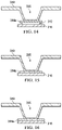
- FIG. 11 illustrates the deposition of the upper sacrificial layer 330 on sacrificial layer 308 (also termed “lower” sacrificial layer).
- the upper sacrificial layer 330 also covers the titanium nitride pad 314 a .
- a photolithography process exposes a via(s) 335 over the titanium nitride pad 314 a where a low resistance interconnect to the metal mirror layer 340 is to be formed.
- the mirror metal 340 (e.g., a reflective aluminum alloy) also deposited on the via walls and via bottom, as is shown in FIG. 11 .
- the mirror metal is further processed in a photolithography pattern and plasma RIE etch and cleanup to separate each pixel's mirror from adjacent pixels.
- the lower and upper sacrificial layers 308 and 330 are selectively removed through the gaps around each pixel.
- the metal that formed in the via 335 remains thereby forming the mirror via 202 shown in FIG. 1 .
- the mirror via 202 resides on the titanium nitride pad 314 a which is on the lower aluminum silicon layer 312 which is on the hinge 216 .
- FIG. 12 illustrates the embodiment in which the lower aluminum silicon layer 312 is absent as noted with respect to FIG. 10 .
- FIG. 13 illustrates the titanium nitride pad 314 a formed in a process that self-aligns the titanium nitride pad to the underlying hinge 216 .
- the titanium nitride pad is initially oversized (e.g., sized to have a footprint larger than the desired size of the final pad). That is, during the etching process to form the titanium nitride pad 314 a , the pad is formed larger than the area of the mirror via to be formed thereon. The excess titanium nitride of the initially oversized titanium nitride pad is removed during the subsequent process operation to form the torsion hinge 216 . As a result, the width W 1 of the hinge 216 and the titanium nitride pad 314 a is the same and the titanium nitride pad is centered on the hinge.
- FIGS. 14-16 illustrate the examples of FIGS. 11-13 , respectively, after the removal of the sacrificial layers 308 and 330 .
- Couple and “couples” mean either an indirect or direct connection. Thus, if a first structure couples to a second structure, that connection may be through a direct connection or through an indirect connection via other structures and connections. Further, in this description, the term “approximately” means plus or minus 10% in some embodiments.
Abstract
Description
Claims (19)
Priority Applications (3)
| Application Number | Priority Date | Filing Date | Title |
|---|---|---|---|
| US15/818,973 US11409098B2 (en) | 2017-11-21 | 2017-11-21 | Mirror via conductivity for DMD pixel |
| PCT/US2018/061980 WO2019104019A1 (en) | 2017-11-21 | 2018-11-20 | Mirror via conductivity for dmd pixel |
| US17/808,309 US11703678B2 (en) | 2017-11-21 | 2022-06-23 | Mirror via conductivity for DMD pixel |
Applications Claiming Priority (1)
| Application Number | Priority Date | Filing Date | Title |
|---|---|---|---|
| US15/818,973 US11409098B2 (en) | 2017-11-21 | 2017-11-21 | Mirror via conductivity for DMD pixel |
Related Child Applications (1)
| Application Number | Title | Priority Date | Filing Date |
|---|---|---|---|
| US17/808,309 Division US11703678B2 (en) | 2017-11-21 | 2022-06-23 | Mirror via conductivity for DMD pixel |
Publications (2)
| Publication Number | Publication Date |
|---|---|
| US20190155016A1 US20190155016A1 (en) | 2019-05-23 |
| US11409098B2 true US11409098B2 (en) | 2022-08-09 |
Family
ID=66532931
Family Applications (2)
| Application Number | Title | Priority Date | Filing Date |
|---|---|---|---|
| US15/818,973 Active 2038-08-28 US11409098B2 (en) | 2017-11-21 | 2017-11-21 | Mirror via conductivity for DMD pixel |
| US17/808,309 Active US11703678B2 (en) | 2017-11-21 | 2022-06-23 | Mirror via conductivity for DMD pixel |
Family Applications After (1)
| Application Number | Title | Priority Date | Filing Date |
|---|---|---|---|
| US17/808,309 Active US11703678B2 (en) | 2017-11-21 | 2022-06-23 | Mirror via conductivity for DMD pixel |
Country Status (2)
| Country | Link |
|---|---|
| US (2) | US11409098B2 (en) |
| WO (1) | WO2019104019A1 (en) |
Citations (7)
| Publication number | Priority date | Publication date | Assignee | Title |
|---|---|---|---|---|
| US20040156089A1 (en) * | 2000-08-11 | 2004-08-12 | Doan Jonathan C. | Hinge structures for micro-mirror arrays |
| US20070258125A1 (en) | 2006-05-08 | 2007-11-08 | Texas Instruments Incorporated | Micro-mirror hinge |
| US20090002805A1 (en) | 2005-10-28 | 2009-01-01 | Miradia Inc. | Projection display system including a high fill ratio silicon spatial light modulator |
| US20090231673A1 (en) * | 2008-03-12 | 2009-09-17 | Texas Instruments Incorporated | Multilayered deformable element with reduced memory properties in a mems device |
| US8501023B2 (en) | 2006-05-24 | 2013-08-06 | Texas Instruments Incorporated | Method for forming a mirror MEMS device |
| US20170050844A1 (en) | 2015-08-17 | 2017-02-23 | Texas Instruments Incorporated | Hermetically-sealed mems device and its fabrication |
| US20170176740A1 (en) * | 2015-12-17 | 2017-06-22 | Texas Instruments Incorporated | Method of fabricating a microelectronic device with buried dark layers |
Family Cites Families (1)
| Publication number | Priority date | Publication date | Assignee | Title |
|---|---|---|---|---|
| US6960305B2 (en) * | 1999-10-26 | 2005-11-01 | Reflectivity, Inc | Methods for forming and releasing microelectromechanical structures |
-
2017
- 2017-11-21 US US15/818,973 patent/US11409098B2/en active Active
-
2018
- 2018-11-20 WO PCT/US2018/061980 patent/WO2019104019A1/en active Application Filing
-
2022
- 2022-06-23 US US17/808,309 patent/US11703678B2/en active Active
Patent Citations (7)
| Publication number | Priority date | Publication date | Assignee | Title |
|---|---|---|---|---|
| US20040156089A1 (en) * | 2000-08-11 | 2004-08-12 | Doan Jonathan C. | Hinge structures for micro-mirror arrays |
| US20090002805A1 (en) | 2005-10-28 | 2009-01-01 | Miradia Inc. | Projection display system including a high fill ratio silicon spatial light modulator |
| US20070258125A1 (en) | 2006-05-08 | 2007-11-08 | Texas Instruments Incorporated | Micro-mirror hinge |
| US8501023B2 (en) | 2006-05-24 | 2013-08-06 | Texas Instruments Incorporated | Method for forming a mirror MEMS device |
| US20090231673A1 (en) * | 2008-03-12 | 2009-09-17 | Texas Instruments Incorporated | Multilayered deformable element with reduced memory properties in a mems device |
| US20170050844A1 (en) | 2015-08-17 | 2017-02-23 | Texas Instruments Incorporated | Hermetically-sealed mems device and its fabrication |
| US20170176740A1 (en) * | 2015-12-17 | 2017-06-22 | Texas Instruments Incorporated | Method of fabricating a microelectronic device with buried dark layers |
Non-Patent Citations (3)
| Title |
|---|
| Benjamin Lee, DMD 101: Introduction to Digital Micormirror Device (DMD) Technology. Application Report DLPA008A-Jul. 2008-Revised Oct. 2013. |
| International Search Report for PCT/US2018/061980 dated Feb. 21, 2019. |
| Zapevalin, A.I. Overview of Gas-Phase Chemistry Used for Plasma Chemical Etching Si, SIO2 and SI3N4; Penza State University; printed Feb. 21, 2019; pp. 2-6. |
Also Published As
| Publication number | Publication date |
|---|---|
| WO2019104019A1 (en) | 2019-05-31 |
| WO2019104019A9 (en) | 2019-08-15 |
| US20190155016A1 (en) | 2019-05-23 |
| US20220326508A1 (en) | 2022-10-13 |
| US11703678B2 (en) | 2023-07-18 |
Similar Documents
| Publication | Publication Date | Title |
|---|---|---|
| US5646768A (en) | Support posts for micro-mechanical devices | |
| US6870660B2 (en) | Digital micromirror device having mirror-attached spring tips | |
| US6861277B1 (en) | Method of forming MEMS device | |
| US7618835B2 (en) | Fabricating a spatial light modulator | |
| US20080074725A1 (en) | Micro devices having anti-stiction materials | |
| US7471440B2 (en) | Fabricating micro devices using sacrificial materials | |
| KR20170043495A (en) | A resistive random access memory (rram) with improved forming voltage characteristics and method for making | |
| US7405862B2 (en) | Spatial light modulator having a cantilever anti-stiction mechanism | |
| EP0812472A1 (en) | Method for forming a structure using redeposition | |
| US20100025797A1 (en) | Device Comprising an Ohmic Via Contact, and Method of Fabricating Thereof | |
| US11703678B2 (en) | Mirror via conductivity for DMD pixel | |
| US11120941B2 (en) | Methods of forming capacitors | |
| US8501023B2 (en) | Method for forming a mirror MEMS device | |
| US7354865B2 (en) | Method for removal of pattern resist over patterned metal having an underlying spacer layer | |
| US7072094B2 (en) | Via adhesion in multilayer MEMS structure | |
| US11953674B2 (en) | Microelectromechanical system (MEMS) structure and method of formation | |
| US11511989B2 (en) | MEMS via with enhanced electrical and mechanical integrity | |
| US6773967B1 (en) | Method to prevent antifuse Si damage using sidewall spacers | |
| US20070166863A1 (en) | Method for forming mirror devices for a digital light process apparatus | |
| US20220399495A1 (en) | Resistive random-access memory (rram) device and forming method thereof | |
| KR100195640B1 (en) | Method for fabricating an optical projection system | |
| KR19980014717A (en) | Optical path control device with uniform stress distribution and method of manufacturing the same | |
| JP2006201541A (en) | Method for forming mirror substrate | |
| JPH01228146A (en) | Manufacture of semiconductor device |
Legal Events
| Date | Code | Title | Description |
|---|---|---|---|
| AS | Assignment |
Owner name: TEXAS INSTRUMENTS INCORPORATED, TEXAS Free format text: ASSIGNMENT OF ASSIGNORS INTEREST;ASSIGNORS:SHERWIN, LUCIUS M.;YUAN, JESSE;BOORANANUT, NOPPAWAN;REEL/FRAME:044188/0272 Effective date: 20171113 |
|
| FEPP | Fee payment procedure |
Free format text: ENTITY STATUS SET TO UNDISCOUNTED (ORIGINAL EVENT CODE: BIG.); ENTITY STATUS OF PATENT OWNER: LARGE ENTITY |
|
| STPP | Information on status: patent application and granting procedure in general |
Free format text: DOCKETED NEW CASE - READY FOR EXAMINATION |
|
| STPP | Information on status: patent application and granting procedure in general |
Free format text: NON FINAL ACTION MAILED |
|
| STPP | Information on status: patent application and granting procedure in general |
Free format text: RESPONSE TO NON-FINAL OFFICE ACTION ENTERED AND FORWARDED TO EXAMINER |
|
| STPP | Information on status: patent application and granting procedure in general |
Free format text: RESPONSE TO NON-FINAL OFFICE ACTION ENTERED AND FORWARDED TO EXAMINER |
|
| STPP | Information on status: patent application and granting procedure in general |
Free format text: NON FINAL ACTION MAILED |
|
| STPP | Information on status: patent application and granting procedure in general |
Free format text: RESPONSE TO NON-FINAL OFFICE ACTION ENTERED AND FORWARDED TO EXAMINER |
|
| STPP | Information on status: patent application and granting procedure in general |
Free format text: FINAL REJECTION MAILED |
|
| STPP | Information on status: patent application and granting procedure in general |
Free format text: DOCKETED NEW CASE - READY FOR EXAMINATION |
|
| STPP | Information on status: patent application and granting procedure in general |
Free format text: NON FINAL ACTION MAILED |
|
| STPP | Information on status: patent application and granting procedure in general |
Free format text: RESPONSE TO NON-FINAL OFFICE ACTION ENTERED AND FORWARDED TO EXAMINER |
|
| STPP | Information on status: patent application and granting procedure in general |
Free format text: NOTICE OF ALLOWANCE MAILED -- APPLICATION RECEIVED IN OFFICE OF PUBLICATIONS |
|
| STPP | Information on status: patent application and granting procedure in general |
Free format text: DOCKETED NEW CASE - READY FOR EXAMINATION |
|
| STPP | Information on status: patent application and granting procedure in general |
Free format text: NOTICE OF ALLOWANCE MAILED -- APPLICATION RECEIVED IN OFFICE OF PUBLICATIONS |
|
| STCF | Information on status: patent grant |
Free format text: PATENTED CASE |