US11393879B2 - Light-emitting device, display device, photoelectric conversion device, electronic apparatus, illumination device, and mobile body - Google Patents
Light-emitting device, display device, photoelectric conversion device, electronic apparatus, illumination device, and mobile body Download PDFInfo
- Publication number
- US11393879B2 US11393879B2 US17/022,687 US202017022687A US11393879B2 US 11393879 B2 US11393879 B2 US 11393879B2 US 202017022687 A US202017022687 A US 202017022687A US 11393879 B2 US11393879 B2 US 11393879B2
- Authority
- US
- United States
- Prior art keywords
- light
- emitting
- dummy
- elements
- layer
- Prior art date
- Legal status (The legal status is an assumption and is not a legal conclusion. Google has not performed a legal analysis and makes no representation as to the accuracy of the status listed.)
- Active, expires
Links
Images


Classifications
-
- H01L27/3218—
-
- H—ELECTRICITY
- H10—SEMICONDUCTOR DEVICES; ELECTRIC SOLID-STATE DEVICES NOT OTHERWISE PROVIDED FOR
- H10K—ORGANIC ELECTRIC SOLID-STATE DEVICES
- H10K59/00—Integrated devices, or assemblies of multiple devices, comprising at least one organic light-emitting element covered by group H10K50/00
- H10K59/80—Constructional details
- H10K59/88—Dummy elements, i.e. elements having non-functional features
-
- H01L27/322—
-
- H01L27/3223—
-
- H01L27/3234—
-
- H01L51/5271—
-
- H—ELECTRICITY
- H10—SEMICONDUCTOR DEVICES; ELECTRIC SOLID-STATE DEVICES NOT OTHERWISE PROVIDED FOR
- H10K—ORGANIC ELECTRIC SOLID-STATE DEVICES
- H10K50/00—Organic light-emitting devices
- H10K50/80—Constructional details
- H10K50/85—Arrangements for extracting light from the devices
- H10K50/856—Arrangements for extracting light from the devices comprising reflective means
-
- H—ELECTRICITY
- H10—SEMICONDUCTOR DEVICES; ELECTRIC SOLID-STATE DEVICES NOT OTHERWISE PROVIDED FOR
- H10K—ORGANIC ELECTRIC SOLID-STATE DEVICES
- H10K59/00—Integrated devices, or assemblies of multiple devices, comprising at least one organic light-emitting element covered by group H10K50/00
- H10K59/30—Devices specially adapted for multicolour light emission
- H10K59/35—Devices specially adapted for multicolour light emission comprising red-green-blue [RGB] subpixels
- H10K59/353—Devices specially adapted for multicolour light emission comprising red-green-blue [RGB] subpixels characterised by the geometrical arrangement of the RGB subpixels
-
- H—ELECTRICITY
- H10—SEMICONDUCTOR DEVICES; ELECTRIC SOLID-STATE DEVICES NOT OTHERWISE PROVIDED FOR
- H10K—ORGANIC ELECTRIC SOLID-STATE DEVICES
- H10K59/00—Integrated devices, or assemblies of multiple devices, comprising at least one organic light-emitting element covered by group H10K50/00
- H10K59/30—Devices specially adapted for multicolour light emission
- H10K59/38—Devices specially adapted for multicolour light emission comprising colour filters or colour changing media [CCM]
-
- H—ELECTRICITY
- H10—SEMICONDUCTOR DEVICES; ELECTRIC SOLID-STATE DEVICES NOT OTHERWISE PROVIDED FOR
- H10K—ORGANIC ELECTRIC SOLID-STATE DEVICES
- H10K59/00—Integrated devices, or assemblies of multiple devices, comprising at least one organic light-emitting element covered by group H10K50/00
- H10K59/80—Constructional details
- H10K59/875—Arrangements for extracting light from the devices
- H10K59/876—Arrangements for extracting light from the devices comprising a resonant cavity structure, e.g. Bragg reflector pair
-
- H—ELECTRICITY
- H10—SEMICONDUCTOR DEVICES; ELECTRIC SOLID-STATE DEVICES NOT OTHERWISE PROVIDED FOR
- H10K—ORGANIC ELECTRIC SOLID-STATE DEVICES
- H10K59/00—Integrated devices, or assemblies of multiple devices, comprising at least one organic light-emitting element covered by group H10K50/00
- H10K59/80—Constructional details
- H10K59/875—Arrangements for extracting light from the devices
- H10K59/878—Arrangements for extracting light from the devices comprising reflective means
-
- H—ELECTRICITY
- H10—SEMICONDUCTOR DEVICES; ELECTRIC SOLID-STATE DEVICES NOT OTHERWISE PROVIDED FOR
- H10K—ORGANIC ELECTRIC SOLID-STATE DEVICES
- H10K59/00—Integrated devices, or assemblies of multiple devices, comprising at least one organic light-emitting element covered by group H10K50/00
- H10K59/60—OLEDs integrated with inorganic light-sensitive elements, e.g. with inorganic solar cells or inorganic photodiodes
- H10K59/65—OLEDs integrated with inorganic image sensors
Definitions
- the present invention relates to a light-emitting device, a display device, a photoelectric conversion device, an electronic apparatus, an illumination device, and a mobile body.
- a light-emitting device including an organic EL light-emitting element has been attracting attention.
- a method (to be referred to as a white+CF method hereinafter) that uses a light-emitting element that emits white light and a color filter to increase the resolution of the light-emitting device.
- the white+CF method an organic layer is formed on the entire surface of the substrate. Therefore, compared to a method of forming an organic layer for each color using a metal mask, the white+CF method is relatively easy to achieve a high resolution for the pixel size, the pitch between pixels, or the like.
- 2017-146374 describes a white+CF type electrooptical device in which a pixel electrode provided for each pixel is formed by a transparent conductive film, and a power supply line serving as a reflective layer is arranged between the pixel electrode and the substrate. By constructing the optical resonance structure between the reflective layer and the counter electrode, the light extraction efficiency and color reproducibility are improved. Further, Japanese Patent Laid-Open No. 2017-146374 describes that the electrooptical device includes a display region in which an image is displayed by driving pixels, and a peripheral region which is adjacent to the display region and in which dummy pixels each having a structure similar to that of the pixel but do not contribute to image display are arranged.
- the counter electrode is formed on the uneven shape corresponding to the film thickness of the optical path adjustment layer.
- the unevenness corresponding to the film thickness of the optical path adjustment layer is formed not only in the display region but also in the peripheral region. If the uneven shape becomes large, a thin film portion can be generated in the counter electrode when the counter electrode is formed. If the thin film portion is generated in the counter electrode, the resistance of the counter electrode increases, and the resistance in the supply path of the power for driving the pixels in the display region increases, which may lead to a rise in driving voltage.
- Each of some embodiments of the present invention provides a technique advantageous in suppressing a rise in driving voltage of a light-emitting device.
- a light-emitting device comprising a display region for displaying an image, in which a first light-emitting element and a second light-emitting element are arranged, and a dummy region in which a first dummy element and a second dummy element are arranged and which does not display an image
- each of the first light-emitting element, the second light-emitting element, the first dummy element, and the second dummy element includes a reflective layer arranged on a substrate, a first electrode arranged above the reflective layer, a light-emitting layer arranged above the first electrode, and a second electrode arranged above the light-emitting layer, a distance from the reflective layer to the light-emitting layer in the first light-emitting element is different from a distance from the reflective layer to the light-emitting layer in the second light-emitting element, and where a difference between the distance from the reflective layer to the light-emitting layer in the first light-emit
- a light-emitting device comprising a display region for displaying an image, in which a first light-emitting element and a second light-emitting element are arranged, and a dummy region in which a first dummy element and a second dummy element are arranged and which does not display an image
- each of the first light-emitting element, the second light-emitting element, the first dummy element, and the second dummy element includes a reflective layer arranged on a substrate, a first electrode arranged above the reflective layer, a light-emitting layer arranged above the first electrode, a second electrode arranged above the light-emitting layer, and an insulating layer arranged between the reflective layer and the first electrode, a film thickness of the insulating layer of the first light-emitting element is different from a film thickness of the insulating layer of the second light-emitting element, and where a difference between the film thickness of the insulating layer of first light-e
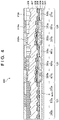
- FIG. 1 is a plan view showing an arrangement example of a light-emitting device according to an embodiment
- FIG. 2 is a sectional view of the light-emitting device shown in FIG. 1 ;
- FIG. 3 is a plan view showing a modification of the light-emitting device shown in FIG. 1 ;
- FIG. 4 is a sectional view of the light-emitting device shown in FIG. 3 ;
- FIG. 5 is a sectional view showing another modification of the light-emitting device shown in FIG. 2 ;
- FIG. 6 is a plan view showing still another modification of the light-emitting device shown in FIG. 1 ;
- FIG. 7 is a plan view showing still another modification of the light-emitting device shown in FIG. 1 ;
- FIG. 8 is a plan view showing still another modification of the light-emitting device shown in FIG. 1 ;
- FIG. 9 is a sectional view showing still another modification of the light-emitting device shown in FIG. 2 ;
- FIG. 10 is a sectional view of a light-emitting device of a comparative example
- FIG. 11 is a view showing an example of a display device using the light-emitting device shown in FIG. 1 ;
- FIG. 12 is a view showing an example of a photoelectric conversion device using the light-emitting device shown in FIG. 1 ;
- FIG. 13 is a view showing an example of an electronic apparatus using the light-emitting device shown in FIG. 1 ;
- FIGS. 14A and 14B are views each showing an example of a display device using the light-emitting device shown in FIG. 1 ;
- FIG. 15 is a view showing an example of an illumination device using the light-emitting device shown in FIG. 1 ;
- FIG. 16 is a view showing an example of a mobile body using the light-emitting device shown in FIG. 1 .
- FIG. 1 is a plan view showing an arrangement example of a light-emitting device 100 in this embodiment.
- the light-emitting device 100 includes a display region 120 for displaying an image, in which a plurality of light-emitting elements 201 are arranged, and a dummy region 121 in which a plurality of dummy elements 202 are arranged and which does not display an image.
- the dummy region 121 may be arranged so as to surround the display region 120 .
- the light-emitting elements 201 and the dummy elements 202 are arranged in a two-dimensional array.
- the dummy element 202 arranged in the dummy region 121 has a structure similar to that of the light-emitting element 201 arranged in the display region 120 , but does not actually contribute to display of the image.
- the dummy element 202 may not emit light.
- the dummy element 202 is, for example, arranged to suppress light reflection outside the display region 120 , and provided with a reflective electrode structure similar to that of the display region 120 .
- the outer edge of the display region 120 may be defined by the outer edge of the outermost light-emitting element 201 among the plurality of light-emitting elements 201 that actually emit light. Alternatively, as shown in FIG. 1 , the outer edge of the display region 120 may be a substantially rectangular shape obtained by connecting the outer edges of the outermost light-emitting elements 201 among the plurality of light-emitting elements 201 that actually emit light.
- FIG. 2 is a schematic sectional view of a boundary portion A between the display region 120 and the dummy region 121 shown in FIG. 1 .
- the light-emitting element 201 is arranged on a substrate 301 in the display region 120
- the dummy element 202 is arranged on the substrate 301 in the dummy region 121 .
- Each of the light-emitting element 201 and the dummy element 202 includes a reflective layer 302 arranged on the substrate 301 , an electrode 304 arranged above the reflective layer 302 , an organic layer 305 including a light-emitting layer arranged on the electrode 304 , and an electrode 306 arranged on the organic layer 305 .
- an insulating layer 303 is arranged between the reflective layer 302 and the electrode 304 (also referred to as a lower electrode or an individual electrode) arranged for each of the light-emitting element 201 and the dummy element 202 .
- a sealing layer 307 and a planarizing layer 308 are arranged on the electrode 306 (also referred to as an upper electrode or a common electrode) shared by the light-emitting element 201 and the dummy element 202 .
- the sealing layer 307 and the planarizing layer 308 are shown as different layers, but they may be formed as one layer. Further, in the arrangement shown in FIG.
- each light-emitting element 201 includes one of color filters 310 ( 310 a , 310 b , and 310 c ) that transmit different colors. This enables the light-emitting device 100 to perform, for example, full-color display.
- the color filter 310 can be arranged in the dummy region 121 .
- the insulating layers 303 a to 303 c arranged in the light-emitting elements 201 a to 201 c , respectively, have different thicknesses to optimize the optical distance from the upper surface of the reflective layer 302 to the light-emitting position of the light-emitting layer of the organic layer 305 in accordance with the colors transmitted by the color filters 310 a to 310 c . It can be said that the plurality of light-emitting elements 201 a to 201 c include the light-emitting elements whose insulating layers 303 have different film thicknesses.
- the insulating layer 303 optimizes the optical distance from the reflective layer 302 to the light-emitting layer of the organic layer 305 , so that it can be also referred to as an optical path adjustment layer.
- the insulating layer 303 arranged in the dummy element 202 does not change in accordance with the color filters 310 a to 310 c arranged in the dummy elements 202 , and the distance from the reflective layer 302 to the light-emitting layer of the organic layer 305 is constant.
- the distance from the reflective layer 302 to the light-emitting layer of the organic layer 305 in the dummy element 202 a is equal to the distance from the reflective layer 302 to the light-emitting layer of the organic layer 305 in the dummy element 202 b .
- the distance from the reflective layer 302 to the light-emitting layer of the organic layer 305 in the dummy element 202 a is equal to the distance from the reflective layer 302 to the light-emitting layer of the organic layer 305 in the dummy element 202 c .
- the insulating layer 303 arranged in the dummy element 202 has the film thickness similar to that of the insulating layer 303 c arranged in the light-emitting element 201 c.
- the difference between the distance from the reflective layer 302 to the light-emitting layer of the organic layer 305 in the light-emitting element 201 a and the distance from the reflective layer 302 to the light-emitting layer of the organic layer 305 in the light-emitting element 201 b is set as the first difference.
- the difference between the distance from the reflective layer 302 to the light-emitting layer of the organic layer 305 in the dummy element 202 a and the distance from the reflective layer 302 to the light-emitting layer of the organic layer 305 in the dummy element 202 b or 202 c is set as the second difference. In this case, the second difference is smaller than the first difference.
- the second difference is smaller than the first difference.
- the second difference is smaller than the first difference.
- the difference in distance from the reflective layer 302 to the light-emitting layer of the organic layer 305 between any two of the plurality of dummy elements 202 a to 202 c is smaller than the difference between the distance from the reflective layer 302 to the light-emitting layer of the organic layer 305 in the light-emitting element 201 b having the largest distance among the plurality of light-emitting elements 201 a to 201 c , and the distance in the light-emitting element 201 c having the smallest distance among them.
- the difference in distance from the reflective layer 302 to the light-emitting layer of the organic layer 305 can be the difference in film thickness of the insulating layer 303 arranged in each of the light-emitting elements 201 a to 201 c and the dummy elements 202 a to 202 c . The details will be described layer.
- the material of the substrate 301 glass, a plastic, silicon, or the like can be used.
- a switching element such as a transistor, wirings, or the like may be formed in the substrate 301 below the reflective layer 302 (on the side opposite to the organic layer 305 ) via an interlayer insulating film or the like.
- a metal material having a visible light reflectance equal to or larger than 50% may be used for the reflective layer 302 . More specifically, a metal such as aluminum (Al) or silver (Ag), an allow obtained by adding silicon (Si), copper (Cu), nickel (Ni), neodymium (Nd), titanium (Ti), or the like to the metal can be used for the reflective layer 302 .
- the reflective layer 302 may have a stacked structure including, in addition to the layer formed of the above-described material, a barrier layer on the light-reflecting surface.
- a metal such as Ti, tungsten (W), molybdenum (Mo), gold (Au) or an alloy thereof, or a transparent conductive oxide such as indium tin oxide (ITO) or indium zinc oxide (IZO) may be used.
- An inorganic material such as silicon nitride (SiN), silicon oxynitride (SiON), or silicon oxide (SiO) can be used for the insulating layer 303 .
- the insulating layer 303 can be formed using a known technique such as a sputtering method or a chemical vapor deposition method (CVD method).
- the insulating layer 303 can also be formed using an organic material such as an acrylic resin or a polyimide resin.
- the insulating layer 303 may have a stacked structure formed by a plurality of layers. In this embodiment, an example in which the insulating layers 303 have three types of film thicknesses is shown, but the present invention is not limited thereto.
- the film thicknesses of the insulating layers 303 a to 303 c for optimizing the distance (optical distance) between the reflective layer 302 and the light-emitting layer of the organic layer 305 in each of the light-emitting elements 201 a to 201 c for the respective colors transmitted by the color filters 310 a to 310 c will be described.
- Lr represents the optical path length from the upper surface of the reflective layer 302 to the light-emitting layer of the organic layer 305
- ⁇ r represents the phase shift in the reflective layer 302 :
- Lr ⁇ 2 m ⁇ ( ⁇ r / ⁇ ) ⁇ ( ⁇ /4) (1) where m is an integer (non-negative integer) equal to or larger than 0.
- the optical distances of the insulating layers 303 a to 303 c are optimized for respective colors so as to approximately satisfy equation (1).
- the electrode 304 can be a transparent conductive film that transmits visible light, and ITO, IZO, aluminum zinc oxide (AZO), indium gallium zinc oxide (IGZO), or the like is used.
- a partition 309 may be provided in the outer peripheral portion of the electrode 304 in each of the light-emitting element 201 and the dummy element 202 .
- the partition 309 is provided so as to cover the end portion of the outer edge of the electrode 304 , and an opening is provided so that a part of the center of the electrode 304 is exposed.
- An inorganic material such as SiN, SiON, or SiO may be used for the partition 309 .
- the partition 309 may be formed using a known technique such as a sputtering method or a CVD method. Further, an organic material such as an acrylic resin or a polyimide resin may be used for the partition 309 .
- the organic layer 305 is arranged on the electrode 304 , and can be formed using a known technique such as a vapor deposition method or a spin coating method.
- the organic layer 305 may be formed by a plurality of layers including the light-emitting layer. Examples of the plurality of layers include a hole injection layer, a hole transport layer, an electron block layer, the light-emitting layer, a hole block layer, an electron transport layer, and an electron injection layer.
- the organic layer 305 emits light when holes injected from the anode and electrons injected from the cathode are recombined in the light-emitting layer.
- the light-emitting layer may be formed by a single layer or a plurality of layers.
- Each light-emitting layer can include a red light-emitting material, a green light-emitting material, or a blue light-emitting material, and it is also possible to obtain white light by mixing the respective emitted colors. Further, each light-emitting layer may include light-emitting materials having a complementary color relationship such as a blue light-emitting material and a yellow light-emitting material.
- the organic layer 305 may be shared by the plurality of light-emitting elements 201 and the plurality of dummy elements 202 . However, the present invention is not limited to this, and all or part of the organic layer 305 may be patterned for each or some light-emitting elements 201 or for each or some dummy elements 202 .
- the electrode 306 is arranged on the organic layer 305 , and has translucency.
- the electrode 306 may be a semi-transmissive material having a property (that is, semi-transmissive reflectivity) of transmitting part of the light reaching its surface and reflecting the other part of the light.
- a transparent material such as a transparent conductive oxide, or a semi-transmissive material such as a metal such as Al, Ag, or Au, an alkali metal such as lithium (Li) or cesium (Cs), an alkali earth metal such as magnesium (Mg), calcium (Ca), or barium (Ba), or an alloy material containing these metal materials.
- the semi-transmissive material used for the electrode 306 may be an alloy containing Mg or Ag as a main component.
- the electrode 306 may have a stacked structure of the above-described materials.
- the electrode 306 can have any structure as long as it has a suitable transmittance and conductivity.
- the electrode 306 is shared over the light-emitting elements 201 and the dummy elements 202 as shown in FIG. 2 .
- the electrode 304 is the anode and the electrode 306 is the cathode, but the electrode 304 may be the cathode and the electrode 306 may be the anode.
- the sealing layer 307 is formed so as to cover the organic layer 305 including the light-emitting layer.
- the sealing layer 307 may include an inorganic material having translucency and low permeability of oxygen and moisture from the outside.
- an inorganic material such as SiN, SiON, SiO, aluminum oxide (Al 2 O 3 ), or titanium oxide (TiO 2 ) can be used. From the viewpoint of sealing performance, SiN, SiON, or Al 2 O 3 may be used.
- a CVD method, an atomic layer deposition method (ALD method), a sputtering method, or the like can be used to form the sealing layer 307 .
- the sealing layer 307 may have a single-layer structure, or a stacked structure obtained by combining the above-described materials or forming methods.
- the sealing layer 307 is arranged over the plurality of light-emitting elements 201 and the plurality of dummy elements 202 .
- the planarizing layer 308 is formed on the sealing layer 307 .
- the planarizing layer 308 may be formed of an inorganic material or an organic material as long as the material has translucency.
- the sealing layer 307 may be formed by applying an organic material.
- the color filter 310 is arranged on the planarizing layer 308 .
- the color filters 310 a , 310 b , and 310 c are color filters that transmit different colors.
- each of the light-emitting elements 201 a , 201 b , and 201 c it is possible to regard each of the light-emitting elements 201 a , 201 b , and 201 c as a sub pixel, and regard the three sub pixels as one main pixel.
- the color filters 310 a , 310 b , and 310 c may be color filters that transmit red, green, and blue light, respectively. The additive color mixture of these sub pixels enables the light-emitting device 100 to perform full-color display.
- the planar array of the light-emitting elements 201 a , 201 b , and 201 c may be any of a stripe array, a square array, a delta array, a pentile array, and a Bayer array.
- FIG. 10 shows a sectional view of a light-emitting device 110 in a comparative example.
- the dummy elements 202 a to 202 c include insulating layers 303 a to 303 c , respectively, having different film thicknesses. That is, the film thickness of the insulating layer 303 is different among the dummy elements 202 a to 202 c (sub pixels), so that steps are formed on the upper surface of the organic layer 305 .
- the electrode 306 is formed on the upper surface of the organic layer 305 over the entire area of the display region 120 and the dummy region 121 . Therefore, the unevenness of the electrode 306 becomes large in accordance with the difference in film thickness among the insulating layers 303 a to 303 c for the respective sub pixels.
- the light-emitting device 100 includes a contact region 122 for supplying a potential to the electrode 306 such that the dummy region 121 is arranged between the contact region 122 and the display region 120 .
- the contact region 122 connects the electrode 306 to the cathode potential from outside the dummy region 121 .
- the contact regions 122 may be arranged so as to surround the display region 120 and the dummy region 121 as shown in FIG. 1 .
- the electric current which flows between the electrode 304 and the electrode 306 to cause the light-emitting layer of the organic layer 305 to emit light, passes through the electrode 306 arranged on the light-emitting elements 201 and the dummy elements 202 and flows into the contact region 122 .
- the steps of the electrode 306 in the dummy region 121 become large, a thin film portion can be generated in the electrode 306 when the electrode 306 is formed. If the thin film portion is generated in the electrode 306 , the resistance of the electrode 306 increases, and the resistance in the supply path of the power for driving the light-emitting elements 201 in the display region 120 increases, which may lead to a rise in driving voltage.
- the insulating layer 303 ( 303 c ) arranged on the reflective layers 302 in the dummy elements 202 a to 202 c has a constant film thickness regardless of the dummy elements 202 a to 202 c . Accordingly, there is no difference in film thickness of the insulating layer 303 among the dummy elements 202 a to 202 c (sub pixels). This can decrease the unevenness of the electrode 306 arranged on the dummy region 121 . Therefore, it is possible to suppress generation of the thin film portion in the electrode 306 formed in the dummy region 121 when the electrode 306 is formed. As a result, a rise in resistance of the electrode 306 in the dummy region 121 is suppressed, and a rise in driving voltage of the light-emitting device 100 is suppressed.
- the thickness of the insulating layer 303 arranged in the dummy region 121 is set to be equal to the thickness of the insulating layer 303 c arranged in the light-emitting element 201 c , but the present invention is not limited to this.
- the thickness of the insulating layer 303 arranged in the dummy region 121 may be equal to the film thickness of the insulating layer 303 a or the insulating layer 303 b .
- the insulating layer 303 arranged in the dummy element 202 has the film thickness equal to the film thickness of any of the insulating layers 303 a to 303 c arranged in the light-emitting elements 201 , it is possible to decrease the step of the electrode 306 in the dummy region 121 without increasing the number of processing steps.
- the thickness of the insulating layer 303 arranged in the dummy region 121 may be different from the film thicknesses of the insulating layers 303 a to 303 c.
- FIG. 3 is a plan view showing an arrangement example of a light-emitting device 400 of this embodiment.
- FIG. 4 is a schematic sectional view of a boundary portion B between the display region 120 and the dummy region 121 shown in FIG. 3 .
- the light-emitting device 400 further includes, between the display region 120 and the dummy region 121 , an intermediate region 123 in which a plurality of intermediate dummy elements 401 are arranged and which does not display an image.
- the intermediate dummy element 401 arranged in the intermediate region 123 may not emit light.
- the dummy region 121 is a region in which the film thickness of the insulating layer 303 is the same among the dummy elements 202 a to 202 c so there is no difference in film thickness between the reflective layer 302 and the electrode 304 among the dummy elements 202 .
- the plurality of intermediate dummy elements 401 include intermediate dummy elements 401 a to 401 c that have different distances between the reflective layers 302 and the light-emitting layer of the organic layer 305 .
- the difference between the distance from the reflective layer 302 to the light-emitting layer of the organic layer 305 in the light-emitting element 201 a and the distance from the reflective layer 302 to the light-emitting layer of the organic layer 305 in the light-emitting element 201 b is set as the first difference.
- the difference between the distance from the reflective layer 302 to the light-emitting layer of the organic layer 305 in the intermediate dummy element 401 a and the distance from the reflective layer 302 to the light-emitting layer of the organic layer 305 in the intermediate dummy element 401 b is set as the third difference.
- the first difference is equal to the third difference.
- the first difference is equal to the third difference.
- the first difference is similarly equal to the third difference.
- the difference in distance from the reflective layer 302 to the light-emitting layer of the organic layer 305 between the light-emitting element having the largest distance among the plurality of light-emitting elements 201 a to 201 c and the light-emitting element having the smallest distance among them may be equal to the difference in distance from the reflective layer 302 to the light-emitting layer of the organic layer 305 between the intermediate dummy element having the largest distance among the plurality of intermediate dummy elements 401 a to 401 c and the intermediate dummy element having the smallest distance among them.
- the relationship regarding the arrangement order of the light-emitting elements 201 a to 201 c in the display region 120 and the distances from the reflective layers 302 to the light-emitting layer of the organic layer 305 of the light-emitting elements 201 a to 201 c is similar to the relationship regarding the arrangement order of the intermediate dummy elements 401 a to 401 c in the intermediate region 123 and the distances from the reflective layers 302 to the light-emitting layer of the organic layer 305 of the intermediate dummy elements 401 a to 401 c .
- the intermediate dummy elements 401 a to 401 c in the intermediate region 123 have the arrangement similar to that of the light-emitting elements 201 a to 201 c in the display region 120 , and are arranged in a predetermined similar order. This makes it possible to stabilize the shape of the outermost periphery of the display region 120 upon manufacturing the light-emitting device 400 , and suppress a rise in driving voltage while maintaining the quality of the displayed image.
- the number of the intermediate dummy elements 401 arranged in the intermediate region 123 may be about two, but may be larger than two.
- the number of the intermediate dummy elements 401 arranged between the light-emitting element which is arranged at the outer edge of the display region 120 among the plurality of light-emitting elements 201 and the dummy element which is closest to the light-emitting element among the plurality of dummy elements 202 may be, for example, between two (inclusive) and ten (inclusive).
- FIG. 5 is a sectional view showing an arrangement example of a light-emitting device 500 of this embodiment showing another modification of the light-emitting device 100 described above.
- the color filters 310 a to 310 c are arranged that transmit different colors by the respective dummy elements 202 .
- the common same color filter (color filter 310 b ) is arranged as the color filter 310 arranged in the dummy elements 202 .
- the color filter 310 that transmits light having a wavelength different from the wavelength of light which resonates between the reflective layer 302 and the electrode 306 may be arranged in the plurality of dummy elements 202 .
- the insulating layer 303 c is formed with a film thickness that makes the optical distance from the reflective layer 302 to the light-emitting layer of the organic layer 305 optimal for blue.
- the color filter 310 b may be a color filter that transmits red. In this manner, the light which resonates between the reflective layer 302 and the light-emitting layer of the organic layer 305 and the light which is transmitted by the color filter arranged in the dummy element may have a complementary color relationship.
- the electrode 304 of the dummy element 202 and the electrode 304 of the light-emitting element 201 adjacent to the dummy element 202 are short-circuited and the dummy element 202 emits light, the light suitable for the blue color filter is emitted from the organic layer 305 .
- the red color filter 310 b is arranged on the dummy element 202 , unnecessary light emitted by the dummy element 202 is suppressed and further blocked.
- the peak wavelength of the light which resonates between the reflective layer 302 and the light-emitting layer of the organic layer 305 may be different from the peak wavelength of the light which is transmitted by the color filter 310 arranged on the dummy element 202 by 100 nm or more. In this case as well, it is possible to suppress the influence of light emission by the dummy element 202 .
- FIG. 6 is a plan view showing an arrangement example of a light-emitting device 600 of this embodiment.
- the contact regions 122 each for supplying a potential to the electrode 306 do not surround the display region 120 and the dummy region 121 , but are arranged at both X-direction ends in the arrangement shown in FIG. 6 .
- FIG. 6 shows the light-emitting device 600 including the display region 120 in which the light-emitting elements 201 are arranged in a stripe array.
- the plurality of light-emitting elements 201 include a plurality of the light-emitting elements 201 a (denoted by “G” in FIG. 6 ) each provided with, for example, the insulating layer 303 a having the first distance from the reflective layer 302 to the light-emitting layer of the organic layer 305 , and a plurality of the light-emitting elements 201 b (denoted by “R” in FIG. 6 ) each provided with, for example, the insulating layer 303 b having the second distance different from the first distance.
- any one of the plurality of the light-emitting elements 201 b (R) is arranged between the light-emitting elements 201 a (G) adjacent to each other among the plurality of the light-emitting elements 201 a (G).
- the Y direction intersecting the X direction at least either of the plurality of the light-emitting elements 201 a (G) and the plurality of the light-emitting elements 201 b (R) are continuously arranged.
- both the plurality of the light-emitting elements 201 a (G) and the plurality of the light-emitting elements 201 b (R) are continuously arranged.
- the contact region 122 is arranged along the Y direction outside the outer edge of the dummy region 121 intersecting the X direction.
- an electric current which flows from the electrode 304 to the electrode 306 to cause the light-emitting element 201 to emit light flows into the contact region 122 mainly along the X direction.
- an unevenness is generated in the X direction due to the change in film thickness of the insulating layer 303 , and the unevenness in shape of the electrode 306 is larger in the X direction than in the Y direction. Therefore, in the dummy region 121 , the resistance of the electrode 306 can be larger in the X direction than in the Y direction.
- the film thickness of the insulating layer 303 is constant over the dummy elements 202 arranged in the dummy region 121 . Accordingly, in the dummy region 121 , the difference in resistance between the X and Y directions is more suppressed than in the light-emitting device 110 of the comparative example. Thus, it is possible to suppress a rise in voltage for driving the light-emitting elements 201 . In this manner, when the light-emitting elements 201 and the dummy elements 202 provided with the color filters 310 for different colors are arranged in the direction in which the electric current flows, the effect of the structure of the dummy region 121 of this embodiment can be large.
- FIG. 7 is a plan view in a case of a pentile array
- FIG. 8 is a plan view in a case of a square array. As in the stripe array shown in FIG. 6 , a rise in driving voltage can be suppressed.
- FIG. 9 is a plan view showing an arrangement example of a light-emitting device 900 of this embodiment.
- the film thickness of the insulating layer 303 arranged in the dummy element 202 in the dummy region 121 is different among the dummy elements 202 a to 202 c .
- An insulating layer 303 d is arranged in the dummy element 202 a
- an insulating layer 303 e is arranged in the dummy element 202 b
- the insulating layer 303 c is arranged in the dummy element 202 c .
- the difference in distance from the reflective layer 302 to the light-emitting layer of the organic layer 305 between any two of the plurality of dummy elements 202 a to 202 c may be smaller than the difference in distance from the reflective layer 302 to the light-emitting layer of the organic layer 305 between the light-emitting element having the largest distance among the plurality of the light-emitting elements 201 a to 201 c and the light-emitting element having the smallest distance among them.
- the difference in distance from the reflective layer 302 to the light-emitting layer of the organic layer 305 between the dummy element 202 b and the light-emitting element 201 c may be smaller than the difference in distance from the reflective layer 302 to the light-emitting layer of the organic layer 305 between the light-emitting elements 201 b and 201 c .
- the difference between the film thickness of the insulating layer 303 e of the dummy element 202 b and the film thickness of the insulating layer 303 c of the light-emitting element 201 c may be smaller than the difference between the film thickness of the insulating layer 303 b of the light-emitting element 201 b and the film thickness of the insulating layer 303 c of the light-emitting element 201 c .
- the difference in distance from the reflective layer 302 to the light-emitting layer of the organic layer 305 between the dummy elements adjacent to each other among the plurality of the dummy elements 202 a to 202 c may be smaller than the difference in distance from the reflective layer 302 to the light-emitting layer of the organic layer 305 between the light-emitting elements adjacent to each other among the plurality of the light-emitting elements 201 a to 201 c .
- the light-emitting device 100 is applicable to the exposure light source of an electrophotographic image forming device, the backlight of a liquid crystal display device, a light-emitting unit including a color filter in a white light source, and the like.
- the display device may be an image information processing device that includes an image input unit for inputting image information from an area CCD, a linear CCD, a memory card, or the like, and an information processing unit for processing the input information, and displays the input image on a display unit.
- a display unit included in a camera or an inkjet printer may have a touch panel function.
- the driving type of the touch panel function may be an infrared type, a capacitance type, a resistive film type, or an electromagnetic induction type, and is not particularly limited.
- the display device may be used for the display unit of a multifunction printer.
- FIG. 11 is a view schematically showing an example of the display device using the light-emitting device 100 of this embodiment.
- a display device 1000 may include, between an upper cover 1001 and a lower cover 1009 , a touch panel 1003 , a display panel 1005 , a frame 1006 , a circuit board 1007 , and a battery 1008 .
- the touch panel 1003 and the display panel 1005 are connected to flexible printed circuit FPCs 1002 and 1004 , respectively. Active elements such as transistors are arranged on the circuit board 1007 .
- the battery 1008 may not be provided if the display device 1000 is not a portable device, or need not be provided in this position even if the display device is a portable device.
- the above-described light-emitting device 100 in which the light-emitting layer of the organic layer 305 includes an organic light-emitting material such as an organic EL material and which functions as a light-emitting unit can be applied to the display panel 1005 .
- the light-emitting device 100 functioning as the display panel 1005 is connected to the active element such as the transistor arranged on the circuit board 1007 to be operated.
- the display device 1000 shown in FIG. 11 may be used for the display unit of a photoelectric conversion device (image capturing device) that includes an optical unit including a plurality of lenses and an image sensor that receives light passing through the optical unit and photoelectrically converts the light into an electric signal.
- the photoelectric conversion device may include a display unit which displays information acquired by the image sensor.
- the display unit may be a display unit exposed to the outside of the photoelectric conversion device, or a display unit arranged in a viewfinder.
- the photoelectric conversion device may be a digital camera or a digital video camera.
- FIG. 12 is a view schematically showing an example of a photoelectric conversion device using the light-emitting device 100 of this embodiment.
- a photoelectric conversion device 1100 may include a viewfinder 1101 , a rear display 1102 , an operation unit 1103 , and a housing 1104 .
- the photoelectric conversion device 1100 can be referred to as an image capturing device.
- the light-emitting device 100 in which the light-emitting layer of the organic layer 305 includes the organic light-emitting material and which functions as a light-emitting unit can be applied to the viewfinder 1101 serving as the display unit.
- the light-emitting device 100 may display not only an image to be captured, but also environment information, an image capturing instruction, and the like.
- the environment information may include the intensity of ambient light, the direction of ambient light, the moving speed of an object, the possibility that the object is blocked by a shielding object, or the like.
- the above-described light-emitting device 100 in which the light-emitting layer of the organic layer 305 includes the organic light-emitting material can be used in the viewfinder 1101 since the organic light-emitting material has a high response speed.
- the light-emitting device 100 using the organic light-emitting material can be used more suitably than a liquid crystal display device in the devices that require a high display speed.
- the photoelectric conversion device 1100 includes an optical unit (not shown).
- the optical unit includes a plurality of lenses and forms an image on a photoelectric conversion element (not shown), which receives light having passed through the optical unit, housed in the housing 1104 . It is possible to adjust the focus by adjusting the relative positions of the plurality of lenses. This operation can be performed automatically.
- the above-described light-emitting device 100 in which the light-emitting layer of the organic layer 305 includes the organic light-emitting material and which functions as a light-emitting unit may be applied to the display unit of an electronic apparatus.
- the display unit may have both a display function and an operation function.
- the mobile terminal include a mobile phone such as a smartphone, a tablet, and a head mounted display.
- FIG. 13 is a view schematically showing an example of an electronic apparatus using the light-emitting device 100 of this embodiment.
- An electronic apparatus 1200 includes a display unit 1201 , an operation unit 1202 , and a housing 1203 .
- the housing 1203 may include a circuit, a printed board including the circuit, a battery, and a communication unit.
- the operation unit 1202 may be a button or a touch panel type sensing unit.
- the operation unit 1202 may be a biometrics unit that recognizes a fingerprint and releases a lock or the like.
- a mobile apparatus including a communication unit can also be called a communication apparatus.
- the above-described light-emitting device 100 in which the light-emitting layer of the organic layer 305 includes the organic light-emitting material and which functions as a light-emitting unit can be applied to the display unit 1201 .
- FIGS. 14A and 14B are views schematically showing examples of a display device using the light-emitting device 100 of this embodiment.
- FIG. 14A shows a display device such as a television monitor or a PC monitor.
- a display device 1300 includes a frame 1301 and a display unit 1302 .
- the above-described light-emitting device 100 in which the light-emitting layer of the organic layer 305 includes the organic light-emitting material and which functions as a light-emitting unit can be applied to the display unit 1302 .
- the display device 1300 may include a base 1303 that supports the frame 1301 and the display unit 1302 .
- the base 1303 is not limited to the form shown in FIG. 14A .
- the lower side of the frame 1301 may serve as the base 1303 .
- the frame 1301 and the display unit 1302 may be bent.
- the curvature radius may be between 5,000 mm (inclusive) and 6,000 mm (inclusive).
- FIG. 14B is a view schematically showing another example of the display device using the light-emitting device 100 of this embodiment.
- a display device 1310 shown in FIG. 14B is configured to be bendable, and is a so-called foldable display device.
- the display device 1310 includes a first display unit 1311 , a second display unit 1312 , a housing 1313 , and a bending point 1314 .
- the above-described light-emitting device 100 in which the light-emitting layer of the organic layer 305 includes the organic light-emitting material and which functions as a light-emitting unit can be applied to each of the first display unit 1311 and the second display unit 1312 .
- the first display unit 1311 and the second display unit 1312 may be one seamless display device.
- the first display unit 1311 and the second display unit 1312 can be divided at the bending point.
- the first display unit 1311 and the second display unit 1312 may display different images, or one image may be displayed with the first display unit and
- FIG. 15 is a view schematically showing an example of an illumination device using the light-emitting device 100 of this embodiment.
- An illumination device 1400 may include a housing 1401 , a light source 1402 , a circuit board 1403 , an optical film 1404 , and a light diffusion unit 1405 .
- the above-described light-emitting device 100 in which the light-emitting layer of the organic layer 305 includes the organic light-emitting material and which functions as a light-emitting unit can be applied to the light source 1402 .
- the optical film 1404 may be a filter that improves the color rendering property of the light source.
- the light diffusion unit 1405 can effectively diffuse light from the light source to illuminate a wide range for lighting up or the like. A cover may be provided in the outermost portion, as needed.
- the illumination device 1400 may include both the optical film 1404 and the light diffusion unit 1405 , or may include only one of them.
- the illumination device 1400 is, for example, a device that illuminates a room.
- the illumination device 1400 may emit light of white, day white, or any other color from blue to red.
- the illumination device 1400 may include a light control circuit for controlling the light color.
- the illumination device 1400 may include a power supply circuit connected to the light-emitting device 100 which functions as the light source 1402 .
- the power supply circuit is a circuit that converts an AC voltage into a DC voltage. Note that white light has a color temperature of 4200K, and day-white light has a color temperature of 5000K.
- the illumination device 1400 may also include a color filter.
- the illumination device 1400 may include a heat dissipation portion. The heat dissipation portion releases the heat in the device to the outside of the device, and examples thereof include a metal having high specific heat, liquid silicon, and the like.
- FIG. 16 is a view schematically showing an automobile including a tail lamp which is an example of the lighting unit for an automobile using the light-emitting device 100 of this embodiment.
- An automobile 1500 includes a tail lamp 1501 , and may turn on the tail lamp 1501 when a brake operation or the like is performed.
- the light-emitting device 100 of this embodiment may be used in a head lamp as the lighting unit for an automobile.
- the automobile is an example of a mobile body, and the mobile body may be a ship, a drone, an aircraft, a railroad car, or the like.
- the mobile body may include a body and a lighting unit provided in the body. The lighting unit may inform the current position of the body.
- the above-described light-emitting device 100 in which the light-emitting layer of the organic layer 305 includes the organic light-emitting material and which functions as a light-emitting unit can be applied to the tail lamp 1501 .
- the tail lamp 1501 may include a protective member that protects the light-emitting device 100 which functions as the tail lamp 1501 .
- the protective member has a certain degree of strength, and can be made from any material as long as it is transparent.
- the protective member may be made from polycarbonate or the like. Further, the protective member may be made from polycarbonate mixed with furandicarboxylic acid derivative, acrylonitrile derivative, or the like.
- the automobile 1500 may include a body 1503 and windows 1502 attached thereto.
- the window may be a window for checking the front or rear of the automobile, or may a transparent display.
- the above-described light-emitting device 100 in which the light-emitting layer of the organic layer 305 includes the organic light-emitting material and which functions as a light-emitting unit may be used in the transparent display.
- the components such as the electrodes included in the light-emitting device 100 are formed by transparent members.
Landscapes
- Physics & Mathematics (AREA)
- Optics & Photonics (AREA)
- Electroluminescent Light Sources (AREA)
- Optical Filters (AREA)
- Devices For Indicating Variable Information By Combining Individual Elements (AREA)
Abstract
Description
Lr={2m−(Φr/π)}×(λ/4) (1)
where m is an integer (non-negative integer) equal to or larger than 0. The optical distances of the insulating
Ls={2m′−(Φs/π)}×(λ/4)=−(Φs/π)×(λ/4) (2)
Therefore, a total layer interference L approximately satisfies following equation (3):
L=Lr+Ls=(2m−Φ/π)×(λ/4) (3)
where Φ is the sum Φr+Φs of the phase shifts upon reflecting the light having the wavelength λ by the
Claims (23)
Applications Claiming Priority (3)
| Application Number | Priority Date | Filing Date | Title |
|---|---|---|---|
| JP2019-190459 | 2019-10-17 | ||
| JPJP2019-190459 | 2019-10-17 | ||
| JP2019190459A JP7370806B2 (en) | 2019-10-17 | 2019-10-17 | Light-emitting devices, display devices, photoelectric conversion devices, electronic equipment, lighting devices, and moving objects |
Publications (2)
| Publication Number | Publication Date |
|---|---|
| US20210118959A1 US20210118959A1 (en) | 2021-04-22 |
| US11393879B2 true US11393879B2 (en) | 2022-07-19 |
Family
ID=75492227
Family Applications (1)
| Application Number | Title | Priority Date | Filing Date |
|---|---|---|---|
| US17/022,687 Active 2040-10-06 US11393879B2 (en) | 2019-10-17 | 2020-09-16 | Light-emitting device, display device, photoelectric conversion device, electronic apparatus, illumination device, and mobile body |
Country Status (2)
| Country | Link |
|---|---|
| US (1) | US11393879B2 (en) |
| JP (1) | JP7370806B2 (en) |
Cited By (2)
| Publication number | Priority date | Publication date | Assignee | Title |
|---|---|---|---|---|
| US12433126B2 (en) | 2022-04-20 | 2025-09-30 | Canon Kabushiki Kaisha | Light emitting apparatus, display device, photoelectric conversion device, electronic apparatus, and moving body |
| US12477905B2 (en) | 2022-04-28 | 2025-11-18 | Canon Kabushiki Kaisha | Light emitting device, manufacturing method thereof, display device, photoelectric conversion device, electronic apparatus, illumination device, and moving body |
Families Citing this family (12)
| Publication number | Priority date | Publication date | Assignee | Title |
|---|---|---|---|---|
| US11228005B2 (en) * | 2019-01-11 | 2022-01-18 | Joled Inc. | Organic el display panel having dummy light emitting layers and method for manufacturing organic el display panel having dummy light emitting layers |
| KR102729324B1 (en) * | 2019-12-16 | 2024-11-14 | 삼성디스플레이 주식회사 | Display device and fabricating method for display device |
| JP7458847B2 (en) | 2020-03-24 | 2024-04-01 | キヤノン株式会社 | Display and electronic devices |
| JP7522136B2 (en) * | 2020-03-27 | 2024-07-24 | 京東方科技集團股▲ふん▼有限公司 | Display substrate, display method, and display device |
| JP7198250B2 (en) | 2020-10-12 | 2022-12-28 | キヤノン株式会社 | Display device |
| JP7581011B2 (en) | 2020-10-28 | 2024-11-12 | キヤノン株式会社 | Light-emitting device, display device, imaging device, and electronic device |
| TW202243238A (en) * | 2020-12-25 | 2022-11-01 | 日商索尼半導體解決方案公司 | Display apparatus and electronic device |
| KR20230012132A (en) * | 2021-07-14 | 2023-01-26 | 삼성디스플레이 주식회사 | Display device |
| US12575265B1 (en) * | 2021-09-13 | 2026-03-10 | Apple Inc. | Organic light-emitting diode display with optical cavities and silver anodes |
| US20250048909A1 (en) * | 2021-12-29 | 2025-02-06 | Semiconductor Energy Laboratory Co., Ltd. | Display apparatus |
| CN117136396B (en) * | 2022-03-28 | 2026-03-13 | 京东方科技集团股份有限公司 | Display substrates and their fabrication methods, display panels, and display devices. |
| KR20250173050A (en) * | 2024-05-31 | 2025-12-10 | 삼성디스플레이 주식회사 | Display device and manufacturing method thereof |
Citations (11)
| Publication number | Priority date | Publication date | Assignee | Title |
|---|---|---|---|---|
| US20080198298A1 (en) * | 2007-02-16 | 2008-08-21 | Lg.Philips Lcd Co., Ltd. | Backlight unit and display device having the same |
| US20170236842A1 (en) * | 2016-02-17 | 2017-08-17 | Semiconductor Energy Laboratory Co., Ltd. | Semiconductor device and electronic device |
| US20170237039A1 (en) | 2016-02-15 | 2017-08-17 | Seiko Epson Corporation | Electrooptical device, electrooptical device manufacturing method, and electronic apparatus |
| US20170237033A1 (en) * | 2016-02-15 | 2017-08-17 | Seiko Epson Corporation | Electro-optical apparatus and electronic device |
| US20180213142A1 (en) * | 2017-01-23 | 2018-07-26 | Samsung Electronics Co., Ltd. | Image sensor and electronic device comprising the same |
| US20190189969A1 (en) * | 2017-12-14 | 2019-06-20 | Lg Display Co., Ltd. | Electroluminescence Display Apparatus |
| US20190198816A1 (en) * | 2017-12-27 | 2019-06-27 | Lg Display Co., Ltd. | High-aperture-ratio microdisplay with microcavity structure |
| US20200066818A1 (en) * | 2018-08-24 | 2020-02-27 | Seiko Epson Corporation | Light-emitting device and electronic apparatus |
| US20200271987A1 (en) * | 2019-02-22 | 2020-08-27 | Samsung Display Co., Ltd. | Display device |
| US20210098300A1 (en) * | 2017-08-24 | 2021-04-01 | Semiconductor Energy Laboratory Co., Ltd. | Image processing method |
| US20210313361A1 (en) * | 2018-08-13 | 2021-10-07 | Sony Semiconductor Solutions Corporation | Solid-state imaging device and electronic apparatus |
Family Cites Families (6)
| Publication number | Priority date | Publication date | Assignee | Title |
|---|---|---|---|---|
| CN1921136B (en) | 2000-11-27 | 2012-05-09 | 精工爱普生株式会社 | Organic electroluminescent device, and manufacture method thereof |
| JP2011070921A (en) | 2009-09-25 | 2011-04-07 | Nippon Seiki Co Ltd | Light emitting element |
| US8884509B2 (en) | 2011-03-02 | 2014-11-11 | Semiconductor Energy Laboratory Co., Ltd. | Optical device, display device, and lighting device |
| JP6221418B2 (en) | 2013-07-01 | 2017-11-01 | セイコーエプソン株式会社 | LIGHT EMITTING DEVICE AND ELECTRONIC DEVICE |
| JP6833776B2 (en) | 2017-10-19 | 2021-02-24 | キヤノン株式会社 | Light emitting device having a plurality of organic EL elements |
| KR102432663B1 (en) * | 2017-11-30 | 2022-08-12 | 엘지디스플레이 주식회사 | Electroluminescent Display Device |
-
2019
- 2019-10-17 JP JP2019190459A patent/JP7370806B2/en active Active
-
2020
- 2020-09-16 US US17/022,687 patent/US11393879B2/en active Active
Patent Citations (15)
| Publication number | Priority date | Publication date | Assignee | Title |
|---|---|---|---|---|
| US20080198298A1 (en) * | 2007-02-16 | 2008-08-21 | Lg.Philips Lcd Co., Ltd. | Backlight unit and display device having the same |
| US20180205039A1 (en) | 2016-02-15 | 2018-07-19 | Seiko Epson Corporation | Electro-optical device, electro-optical device manufacturing method, and electronic apparatus |
| US10236473B2 (en) | 2016-02-15 | 2019-03-19 | Seiko Epson Corporation | Electro-optical device, electro-optical device manufacturing method, and electronic apparatus |
| US20170237033A1 (en) * | 2016-02-15 | 2017-08-17 | Seiko Epson Corporation | Electro-optical apparatus and electronic device |
| JP2017146374A (en) | 2016-02-15 | 2017-08-24 | セイコーエプソン株式会社 | Electro-optical device, method of manufacturing electro-optical device, and electronic apparatus |
| US9954201B2 (en) | 2016-02-15 | 2018-04-24 | Seiko Epson Corporation | Electrooptical device, electrooptical device manufacturing method, and electronic apparatus |
| US20170237039A1 (en) | 2016-02-15 | 2017-08-17 | Seiko Epson Corporation | Electrooptical device, electrooptical device manufacturing method, and electronic apparatus |
| US20170236842A1 (en) * | 2016-02-17 | 2017-08-17 | Semiconductor Energy Laboratory Co., Ltd. | Semiconductor device and electronic device |
| US20180213142A1 (en) * | 2017-01-23 | 2018-07-26 | Samsung Electronics Co., Ltd. | Image sensor and electronic device comprising the same |
| US20210098300A1 (en) * | 2017-08-24 | 2021-04-01 | Semiconductor Energy Laboratory Co., Ltd. | Image processing method |
| US20190189969A1 (en) * | 2017-12-14 | 2019-06-20 | Lg Display Co., Ltd. | Electroluminescence Display Apparatus |
| US20190198816A1 (en) * | 2017-12-27 | 2019-06-27 | Lg Display Co., Ltd. | High-aperture-ratio microdisplay with microcavity structure |
| US20210313361A1 (en) * | 2018-08-13 | 2021-10-07 | Sony Semiconductor Solutions Corporation | Solid-state imaging device and electronic apparatus |
| US20200066818A1 (en) * | 2018-08-24 | 2020-02-27 | Seiko Epson Corporation | Light-emitting device and electronic apparatus |
| US20200271987A1 (en) * | 2019-02-22 | 2020-08-27 | Samsung Display Co., Ltd. | Display device |
Cited By (2)
| Publication number | Priority date | Publication date | Assignee | Title |
|---|---|---|---|---|
| US12433126B2 (en) | 2022-04-20 | 2025-09-30 | Canon Kabushiki Kaisha | Light emitting apparatus, display device, photoelectric conversion device, electronic apparatus, and moving body |
| US12477905B2 (en) | 2022-04-28 | 2025-11-18 | Canon Kabushiki Kaisha | Light emitting device, manufacturing method thereof, display device, photoelectric conversion device, electronic apparatus, illumination device, and moving body |
Also Published As
| Publication number | Publication date |
|---|---|
| US20210118959A1 (en) | 2021-04-22 |
| JP7370806B2 (en) | 2023-10-30 |
| JP2021068501A (en) | 2021-04-30 |
Similar Documents
| Publication | Publication Date | Title |
|---|---|---|
| US11393879B2 (en) | Light-emitting device, display device, photoelectric conversion device, electronic apparatus, illumination device, and mobile body | |
| JP7549637B2 (en) | Display device | |
| US12532604B2 (en) | Organic device, method of manufacturing the same, display device, photoelectric conversion device, electronic apparatus, illumination device, and moving body | |
| CN101267700B (en) | Display devices and electronic equipment | |
| US10930891B2 (en) | Organic device, display apparatus, image capturing apparatus, illumination apparatus, and moving body | |
| US11527579B2 (en) | Display device and image pickup apparatus | |
| US10734455B2 (en) | Organic device, display apparatus, imaging apparatus, illumination apparatus, mobile apparatus lighting appliance, and mobile apparatus | |
| JP7418086B2 (en) | Semiconductor devices, display devices, display and imaging devices, and photoelectric conversion devices | |
| JP7504580B2 (en) | Electronic devices, display devices, photoelectric conversion devices, electronic equipment, lighting devices, and mobile objects | |
| US12310183B2 (en) | Organic device having an insulating layer with an upper surface including a slope portion with an angle between 50° and 180° with respect to a surface parallel to a main surface | |
| CN113451374A (en) | Display device, electronic device, and moving object | |
| US11545647B2 (en) | Light-emitting apparatus having a groove in the insulating layer between the light-emitting region and an end of the insulating layer | |
| KR102754802B1 (en) | Organic light-emitting device, display apparatus, photoelectric conversion apparatus, and electronic apparatus | |
| JP2021039183A (en) | Semiconductor device, display device, and photoelectric conversion device | |
| JP7500212B2 (en) | Light-emitting device, display/imaging device, and electronic device | |
| CN114447247B (en) | Light emitting, display, photoelectric conversion, illumination device, electronic apparatus, and moving object | |
| JP2023165556A (en) | Light-emitting devices, methods for manufacturing light-emitting devices, display devices, photoelectric conversion devices, electronic devices, lighting devices, mobile objects, and wearable devices | |
| KR20250144903A (en) | Light emitting apparatus, display apparatus, image capturing apparatus, and electronic device |
Legal Events
| Date | Code | Title | Description |
|---|---|---|---|
| FEPP | Fee payment procedure |
Free format text: ENTITY STATUS SET TO UNDISCOUNTED (ORIGINAL EVENT CODE: BIG.); ENTITY STATUS OF PATENT OWNER: LARGE ENTITY |
|
| AS | Assignment |
Owner name: CANON KABUSHIKI KAISHA, JAPAN Free format text: ASSIGNMENT OF ASSIGNORS INTEREST;ASSIGNORS:SANO, HIROAKI;ISHIZUYA, KOJI;REEL/FRAME:056013/0358 Effective date: 20210323 |
|
| STPP | Information on status: patent application and granting procedure in general |
Free format text: DOCKETED NEW CASE - READY FOR EXAMINATION |
|
| STPP | Information on status: patent application and granting procedure in general |
Free format text: NON FINAL ACTION MAILED |
|
| STPP | Information on status: patent application and granting procedure in general |
Free format text: RESPONSE TO NON-FINAL OFFICE ACTION ENTERED AND FORWARDED TO EXAMINER |
|
| STPP | Information on status: patent application and granting procedure in general |
Free format text: NOTICE OF ALLOWANCE MAILED -- APPLICATION RECEIVED IN OFFICE OF PUBLICATIONS |
|
| STPP | Information on status: patent application and granting procedure in general |
Free format text: PUBLICATIONS -- ISSUE FEE PAYMENT VERIFIED |
|
| STCF | Information on status: patent grant |
Free format text: PATENTED CASE |
|
| MAFP | Maintenance fee payment |
Free format text: PAYMENT OF MAINTENANCE FEE, 4TH YEAR, LARGE ENTITY (ORIGINAL EVENT CODE: M1551); ENTITY STATUS OF PATENT OWNER: LARGE ENTITY Year of fee payment: 4 |