US11387115B2 - Silicon mandrel etch after native oxide punch-through - Google Patents
Silicon mandrel etch after native oxide punch-through Download PDFInfo
- Publication number
- US11387115B2 US11387115B2 US16/716,585 US201916716585A US11387115B2 US 11387115 B2 US11387115 B2 US 11387115B2 US 201916716585 A US201916716585 A US 201916716585A US 11387115 B2 US11387115 B2 US 11387115B2
- Authority
- US
- United States
- Prior art keywords
- chamber
- silicon
- plasma
- workpiece
- gas
- Prior art date
- Legal status (The legal status is an assumption and is not a legal conclusion. Google has not performed a legal analysis and makes no representation as to the accuracy of the status listed.)
- Active
Links
Images


Classifications
-
- H—ELECTRICITY
- H01—ELECTRIC ELEMENTS
- H01J—ELECTRIC DISCHARGE TUBES OR DISCHARGE LAMPS
- H01J37/00—Discharge tubes with provision for introducing objects or material to be exposed to the discharge, e.g. for the purpose of examination or processing thereof
- H01J37/32—Gas-filled discharge tubes
- H01J37/32431—Constructional details of the reactor
- H01J37/3244—Gas supply means
-
- H01L21/32137—
-
- H—ELECTRICITY
- H10—SEMICONDUCTOR DEVICES; ELECTRIC SOLID-STATE DEVICES NOT OTHERWISE PROVIDED FOR
- H10P—GENERIC PROCESSES OR APPARATUS FOR THE MANUFACTURE OR TREATMENT OF DEVICES COVERED BY CLASS H10
- H10P50/00—Etching of wafers, substrates or parts of devices
- H10P50/20—Dry etching; Plasma etching; Reactive-ion etching
- H10P50/26—Dry etching; Plasma etching; Reactive-ion etching of conductive or resistive materials
- H10P50/264—Dry etching; Plasma etching; Reactive-ion etching of conductive or resistive materials by chemical means
- H10P50/266—Dry etching; Plasma etching; Reactive-ion etching of conductive or resistive materials by chemical means by vapour etching only
- H10P50/267—Dry etching; Plasma etching; Reactive-ion etching of conductive or resistive materials by chemical means by vapour etching only using plasmas
- H10P50/268—Dry etching; Plasma etching; Reactive-ion etching of conductive or resistive materials by chemical means by vapour etching only using plasmas of silicon-containing layers
-
- H—ELECTRICITY
- H01—ELECTRIC ELEMENTS
- H01J—ELECTRIC DISCHARGE TUBES OR DISCHARGE LAMPS
- H01J37/00—Discharge tubes with provision for introducing objects or material to be exposed to the discharge, e.g. for the purpose of examination or processing thereof
- H01J37/32—Gas-filled discharge tubes
- H01J37/32009—Arrangements for generation of plasma specially adapted for examination or treatment of objects, e.g. plasma sources
- H01J37/32082—Radio frequency generated discharge
- H01J37/32091—Radio frequency generated discharge the radio frequency energy being capacitively coupled to the plasma
-
- H—ELECTRICITY
- H01—ELECTRIC ELEMENTS
- H01J—ELECTRIC DISCHARGE TUBES OR DISCHARGE LAMPS
- H01J37/00—Discharge tubes with provision for introducing objects or material to be exposed to the discharge, e.g. for the purpose of examination or processing thereof
- H01J37/32—Gas-filled discharge tubes
- H01J37/32009—Arrangements for generation of plasma specially adapted for examination or treatment of objects, e.g. plasma sources
- H01J37/32082—Radio frequency generated discharge
- H01J37/321—Radio frequency generated discharge the radio frequency energy being inductively coupled to the plasma
-
- H—ELECTRICITY
- H01—ELECTRIC ELEMENTS
- H01J—ELECTRIC DISCHARGE TUBES OR DISCHARGE LAMPS
- H01J37/00—Discharge tubes with provision for introducing objects or material to be exposed to the discharge, e.g. for the purpose of examination or processing thereof
- H01J37/32—Gas-filled discharge tubes
- H01J37/32009—Arrangements for generation of plasma specially adapted for examination or treatment of objects, e.g. plasma sources
- H01J37/32422—Arrangement for selecting ions or species in the plasma
-
- H01L21/02071—
-
- H01L21/0332—
-
- H01L21/0335—
-
- H01L21/0337—
-
- H01L21/0338—
-
- H01L21/28088—
-
- H01L21/67069—
-
- H01L29/66545—
-
- H—ELECTRICITY
- H10—SEMICONDUCTOR DEVICES; ELECTRIC SOLID-STATE DEVICES NOT OTHERWISE PROVIDED FOR
- H10D—INORGANIC ELECTRIC SEMICONDUCTOR DEVICES
- H10D64/00—Electrodes of devices having potential barriers
- H10D64/01—Manufacture or treatment
- H10D64/013—Manufacture or treatment of electrodes having a conductor capacitively coupled to a semiconductor by an insulator
- H10D64/01302—Manufacture or treatment of electrodes having a conductor capacitively coupled to a semiconductor by an insulator the insulator being formed after the semiconductor body, the semiconductor being silicon
- H10D64/01304—Manufacture or treatment of electrodes having a conductor capacitively coupled to a semiconductor by an insulator the insulator being formed after the semiconductor body, the semiconductor being silicon characterised by the conductor
- H10D64/01318—Manufacture or treatment of electrodes having a conductor capacitively coupled to a semiconductor by an insulator the insulator being formed after the semiconductor body, the semiconductor being silicon characterised by the conductor the conductor comprising a layer of alloy material, compound material or organic material contacting the insulator, e.g. TiN
-
- H—ELECTRICITY
- H10—SEMICONDUCTOR DEVICES; ELECTRIC SOLID-STATE DEVICES NOT OTHERWISE PROVIDED FOR
- H10D—INORGANIC ELECTRIC SEMICONDUCTOR DEVICES
- H10D64/00—Electrodes of devices having potential barriers
- H10D64/01—Manufacture or treatment
- H10D64/017—Manufacture or treatment using dummy gates in processes wherein at least parts of the final gates are self-aligned to the dummy gates, i.e. replacement gate processes
-
- H—ELECTRICITY
- H10—SEMICONDUCTOR DEVICES; ELECTRIC SOLID-STATE DEVICES NOT OTHERWISE PROVIDED FOR
- H10P—GENERIC PROCESSES OR APPARATUS FOR THE MANUFACTURE OR TREATMENT OF DEVICES COVERED BY CLASS H10
- H10P50/00—Etching of wafers, substrates or parts of devices
- H10P50/20—Dry etching; Plasma etching; Reactive-ion etching
- H10P50/24—Dry etching; Plasma etching; Reactive-ion etching of semiconductor materials
- H10P50/242—Dry etching; Plasma etching; Reactive-ion etching of semiconductor materials of Group IV materials
-
- H—ELECTRICITY
- H10—SEMICONDUCTOR DEVICES; ELECTRIC SOLID-STATE DEVICES NOT OTHERWISE PROVIDED FOR
- H10P—GENERIC PROCESSES OR APPARATUS FOR THE MANUFACTURE OR TREATMENT OF DEVICES COVERED BY CLASS H10
- H10P70/00—Cleaning of wafers, substrates or parts of devices
- H10P70/20—Cleaning during device manufacture
- H10P70/27—Cleaning during device manufacture during, before or after processing of conductive materials, e.g. polysilicon or amorphous silicon layers
- H10P70/273—Cleaning during device manufacture during, before or after processing of conductive materials, e.g. polysilicon or amorphous silicon layers the processing being a delineation of conductive layers, e.g. by RIE
-
- H—ELECTRICITY
- H10—SEMICONDUCTOR DEVICES; ELECTRIC SOLID-STATE DEVICES NOT OTHERWISE PROVIDED FOR
- H10P—GENERIC PROCESSES OR APPARATUS FOR THE MANUFACTURE OR TREATMENT OF DEVICES COVERED BY CLASS H10
- H10P72/00—Handling or holding of wafers, substrates or devices during manufacture or treatment thereof
- H10P72/04—Apparatus for manufacture or treatment
- H10P72/0402—Apparatus for fluid treatment
- H10P72/0418—Apparatus for fluid treatment for etching
- H10P72/0421—Apparatus for fluid treatment for etching for drying etching
-
- H—ELECTRICITY
- H10—SEMICONDUCTOR DEVICES; ELECTRIC SOLID-STATE DEVICES NOT OTHERWISE PROVIDED FOR
- H10P—GENERIC PROCESSES OR APPARATUS FOR THE MANUFACTURE OR TREATMENT OF DEVICES COVERED BY CLASS H10
- H10P76/00—Manufacture or treatment of masks on semiconductor bodies, e.g. by lithography or photolithography
- H10P76/40—Manufacture or treatment of masks on semiconductor bodies, e.g. by lithography or photolithography of masks comprising inorganic materials
- H10P76/405—Manufacture or treatment of masks on semiconductor bodies, e.g. by lithography or photolithography of masks comprising inorganic materials characterised by their composition, e.g. multilayer masks
-
- H—ELECTRICITY
- H10—SEMICONDUCTOR DEVICES; ELECTRIC SOLID-STATE DEVICES NOT OTHERWISE PROVIDED FOR
- H10P—GENERIC PROCESSES OR APPARATUS FOR THE MANUFACTURE OR TREATMENT OF DEVICES COVERED BY CLASS H10
- H10P76/00—Manufacture or treatment of masks on semiconductor bodies, e.g. by lithography or photolithography
- H10P76/40—Manufacture or treatment of masks on semiconductor bodies, e.g. by lithography or photolithography of masks comprising inorganic materials
- H10P76/408—Manufacture or treatment of masks on semiconductor bodies, e.g. by lithography or photolithography of masks comprising inorganic materials characterised by their sizes, orientations, dispositions, behaviours or shapes
- H10P76/4083—Manufacture or treatment of masks on semiconductor bodies, e.g. by lithography or photolithography of masks comprising inorganic materials characterised by their sizes, orientations, dispositions, behaviours or shapes characterised by their behaviours during the lithography processes, e.g. soluble masks or redeposited masks
-
- H—ELECTRICITY
- H10—SEMICONDUCTOR DEVICES; ELECTRIC SOLID-STATE DEVICES NOT OTHERWISE PROVIDED FOR
- H10P—GENERIC PROCESSES OR APPARATUS FOR THE MANUFACTURE OR TREATMENT OF DEVICES COVERED BY CLASS H10
- H10P76/00—Manufacture or treatment of masks on semiconductor bodies, e.g. by lithography or photolithography
- H10P76/40—Manufacture or treatment of masks on semiconductor bodies, e.g. by lithography or photolithography of masks comprising inorganic materials
- H10P76/408—Manufacture or treatment of masks on semiconductor bodies, e.g. by lithography or photolithography of masks comprising inorganic materials characterised by their sizes, orientations, dispositions, behaviours or shapes
- H10P76/4085—Manufacture or treatment of masks on semiconductor bodies, e.g. by lithography or photolithography of masks comprising inorganic materials characterised by their sizes, orientations, dispositions, behaviours or shapes characterised by the processes involved to create the masks
-
- H—ELECTRICITY
- H10—SEMICONDUCTOR DEVICES; ELECTRIC SOLID-STATE DEVICES NOT OTHERWISE PROVIDED FOR
- H10P—GENERIC PROCESSES OR APPARATUS FOR THE MANUFACTURE OR TREATMENT OF DEVICES COVERED BY CLASS H10
- H10P76/00—Manufacture or treatment of masks on semiconductor bodies, e.g. by lithography or photolithography
- H10P76/40—Manufacture or treatment of masks on semiconductor bodies, e.g. by lithography or photolithography of masks comprising inorganic materials
- H10P76/408—Manufacture or treatment of masks on semiconductor bodies, e.g. by lithography or photolithography of masks comprising inorganic materials characterised by their sizes, orientations, dispositions, behaviours or shapes
- H10P76/4088—Processes for improving the resolution of the masks
-
- H—ELECTRICITY
- H01—ELECTRIC ELEMENTS
- H01J—ELECTRIC DISCHARGE TUBES OR DISCHARGE LAMPS
- H01J2237/00—Discharge tubes exposing object to beam, e.g. for analysis treatment, etching, imaging
- H01J2237/32—Processing objects by plasma generation
- H01J2237/33—Processing objects by plasma generation characterised by the type of processing
- H01J2237/334—Etching
-
- H—ELECTRICITY
- H10—SEMICONDUCTOR DEVICES; ELECTRIC SOLID-STATE DEVICES NOT OTHERWISE PROVIDED FOR
- H10P—GENERIC PROCESSES OR APPARATUS FOR THE MANUFACTURE OR TREATMENT OF DEVICES COVERED BY CLASS H10
- H10P50/00—Etching of wafers, substrates or parts of devices
- H10P50/20—Dry etching; Plasma etching; Reactive-ion etching
- H10P50/28—Dry etching; Plasma etching; Reactive-ion etching of insulating materials
- H10P50/282—Dry etching; Plasma etching; Reactive-ion etching of insulating materials of inorganic materials
- H10P50/283—Dry etching; Plasma etching; Reactive-ion etching of insulating materials of inorganic materials by chemical means
Definitions
- the present disclosure relates generally to surface treatment of a workpiece, such as semiconductor workpiece.
- the processing of semiconductor workpieces can involve the deposition and removal of different materials layers on a substrate.
- Device dimension and materials thickness continue to decrease in semiconductor processing with shrinking critical dimensions in semiconductor devices.
- material removal with high selectivity to other material can become increasingly important to semiconductor device performance.
- silicon mandrel and silicon replacement gate removal can be of particular importance as such removal can damage spacers and/or leave residue on sub layers.
- One example aspect of the present disclosure is directed to a method for removing a silicon structure disposed on a workpiece.
- the method can include generating species from a process gas in a first chamber using an inductive coupling element.
- the method can include introducing a fluorine containing gas with the species to create a mixture.
- the mixture can include exposing the silicon structure of the workpiece to the mixture to remove at least a portion of the silicon structure.
- FIG. 1 depicts an example silicon mandrel removal process on a structure according to example embodiments of the present disclosure
- FIG. 2 depicts an example silicon mandrel removal process on a structure according to example embodiments of the present disclosure
- FIG. 3 depicts an example plasma processing apparatus according to example embodiments of the present disclosure
- FIG. 4 depicts an example processing platform according to example embodiments of the present disclosure
- FIG. 5 depicts a flow diagram of an example process according to example embodiments of the present disclosure
- FIG. 6 depicts a flow diagram of an example process according to example embodiments of the present disclosure
- FIG. 7 depicts example injection of a fluorine containing gas using post-plasma injection according to example embodiments of the present disclosure.
- FIG. 8 depicts an example plasma processing apparatus according to example embodiments of the present disclosure.
- Example aspects of the present disclosure are directed to processes for removing a silicon mandrel disposed on a workpiece.
- Device dimension and thickness of materials continue to decrease with shrinking critical dimension in semiconductor devices.
- advanced logic and memory e.g. dynamic random-access memory DRAM
- SADP self-aligned double patterning
- a spacer (e.g., SiN) pair structure is first formed with mandrel (e.g. silicon) material in between. Subsequently, the mandrel material is selectively removed with the spacer structure remaining intact.
- the spacer structure further serves as a hardmask in a following anisotropic ion etch process to transfer its pattern to underlying materials.
- SADP self-aligned double patterning
- SAQP self-aligned quadruple patterning
- a silicon (Si) mandrel is about 10-50 nm in size with a height to width ratio (i.e. aspect ratio) of 4-8:1.
- the silicon feature size and selectivity removal requirement is similar between silicon mandrel in SADP/SAQP process and silicon replacement gate used in advanced field-effect transistor (FET) device fabrication.
- an inductively coupled plasma source with very high selectivity can be used to remove silicon mandrel.
- a fluorine containing gas e.g., nitrogen trifluoride (NF 3 ) or tetrafluoromethane (CF 4 ) or other fluorine containing hydrocarbons such as CH 2 F 2 (difluoromethane), CHF 3 (fluoroform), CH 3 F (fluoromethane)
- NF 3 nitrogen trifluoride
- CF 4 tetrafluoromethane
- other fluorine containing hydrocarbons such as CH 2 F 2 (difluoromethane), CHF 3 (fluoroform), CH 3 F (fluoromethane
- one example aspect of the present disclosure is directed to a method for removing a silicon structure disposed on workpiece.
- the method can include generating species from a process gas using an inductive coupling element in a first chamber (e.g., a plasma chamber).
- the method can include introducing a fluorine containing gas (e.g., nitrogen trifluoride (NF 3 ) or tetrafluoromethane (CF 4 ) or other fluorine containing hydrocarbons such as CH 2 F 2 , CHF 3 , CH 3 F) or other fluorine containing hydrocarbons such as CH 2 F 2 (difluoromethane), CHF 3 (fluoroform), CH 3 F (fluoromethane) with the species to create a mixture.
- a fluorine containing gas e.g., nitrogen trifluoride (NF 3 ) or tetrafluoromethane (CF 4 ) or other fluorine containing hydrocarbons such as CH 2 F 2 , CHF 3 ,
- the method can include exposing the silicon structure of the workpiece to the mixture to remove at least a portion of the silicon structure.
- the silicon structure can include silicon mandrel, silicon replacement gate, or any other suitable silicon containing material.
- the process gas can further include hydrogen (H 2 ).
- the process gas can also include an inert gas, such as helium (He), or argon (Ar).
- the fluorine containing gas e.g., nitrogen trifluoride (NF 3 ) or tetrafluoromethane (CF 4 ) or other fluorine containing hydrocarbons such as CH 2 F 2 , CHF 3 , CH 3 F
- the process gas can be admitted into a plasma chamber and a plasma can be induced using the inductively coupled plasma source to generate a mixture.
- the silicon structure e.g., silicon mandrel or silicon replacement gate
- the workpiece can be exposed to the mixture (e.g., after filtering through a separation grid) to be selectively removed.
- the process gas can include inert gas.
- the inert gas can be admitted into the plasma chamber.
- the fluorine containing gas e.g., NF 3 or CF 4 or other fluorine containing hydrocarbons such as CH 2 F 2 , CHF 3 , CH 3 F
- the fluorine containing gas can be injected outside of the plasma chamber and at downstream flow location from the plasma chamber.
- the fluorine containing gas e.g., NF 3 or CF 4 or other fluorine containing hydrocarbons such as CH 2 F 2 , CHF 3 , CH 3 F
- the post-plasma gas injection gas source can be located between a first grid plate and a second grid plate of a separation grid that can separate the plasma chamber from a processing chamber.
- the post plasma gas injection gas source can be located beneath the separation grid in the processing chamber.
- the method can further include generating a capacitively coupled plasma using a plasma source.
- the method can include exposing the silicon mandrel or silicon replacement gate structures on the workpiece to the capacitively coupled plasma to remove at least a portion of a native oxide layer on top of the silicon mandrels or silicon replacement gates.
- the capacitively coupled plasma can be generated in a processing chamber of a separate plasma processing apparatus relative to the inductively coupled plasma source used to perform the silicon mandrel or silicon replacement grate removal process.
- the native oxide punch-through process and the silicon mandrel or silicon replacement gate removal process can be performed in a processing platform with vacuum transfer (or near vacuum transfer) between processing chambers of separate processing apparatuses.
- the workpiece can be placed into a first processing chamber of a first plasma processing apparatus to perform a native oxide punch-through process using a capacitively coupled plasma source.
- the workpiece can be transferred to a second processing chamber of a second plasma processing apparatus using a workpiece handling robot in a transfer chamber.
- the second plasma processing apparatus can generate an inductively coupled plasma to remove the silicon mandrels or silicon replacement gates according to example aspects of the present disclosure after the native oxide punch-through process.
- the capacitively coupled plasma can be generated in a processing chamber using the same plasma processing apparatus as the plasma processing apparatus used to perform a silicon mandrel or silicon replacement gate removal.
- a workpiece can include a silicon mandrel or silicon replacement gate at least partially covered by a native oxide layer.
- the workpiece can be placed into a processing chamber for silicon mandrel or silicon replacement gate removal process.
- a native oxide punch-through process can be performed by a capacitively coupled plasma induced in the processing chamber to remove the native oxide layer on top of the silicon mandrel or silicon replacement gate.
- an indirect or remote inductively coupled plasma can be used for silicon mandrel or silicon replacement gate removal process.
- Example aspects of the present disclosure provide a number of technical effects and benefits.
- ICP inductively coupled plasma source
- CCP capacitively coupled plasma source
- silicon mandrels or silicon replacement gates can be removed completely with reduced damages on spacer (e.g., SiN spacers) and sublayer (e.g., oxide sublayers, TiN sublayers) materials.
- Process Pressure about 200 mTorr to about 1000 mTorr (e.g., about 600 mTorr)
- Inductively Coupled Plasma Source Power about 600 W to about 2500 W (e.g., about 1500 W)
- Capacitively Coupled Plasma Source Power about 0 W to about 150 W (e.g., about 50 W)
- Workpiece Temperature (20° C.) about 5° C. to 90° C. (e.g., about 20° C.)
- Process Period about 10 seconds to 200 seconds (e.g., 40 seconds)
- FIG. 1 depicts an example silicon mandrel removal process on a structure 50 according to example embodiments of the present disclosure.
- the structure 50 includes a spacer layer 52 (e.g., SiN spacer layer), a silicon mandrel 54 , a sublayer 56 (e.g., an oxide layer), and a substrate 58 (e.g., a silicon substrate).
- the structure 50 can include a plurality of sublayers (e.g., silicon nitride layers, oxide layers, etc.) disposed on the substrate 58 .
- a spacer open process 60 can be conducted on the structure 50 to remove one or more portions of the spacer layer 52 that covers the silicon mandrel 54 such that the silicon mandrel 54 can be exposed. Subsequent to removing the spacer layer 52 on top of the silicon mandrel 54 , a silicon mandrel removal process 70 can be conducted on the structure 50 to remove the silicon mandrel 54 .
- the silicon mandrel removal process 70 exposes the silicon mandrel 54 to an inductively coupled plasma induced in a process gas (e.g., H 2 /He/NF 3 , H 2 /Ar/NF 3 , H 2 /He/CF 4 , or H 2 /Ar/CF 4 ).
- a process gas e.g., H 2 /He/NF 3 , H 2 /Ar/NF 3 , H 2 /He/CF 4 , or H 2 /Ar/CF 4 ).
- the spacer open process 60 and the silicon mandrel removal process 70 can be performed in the same processing apparatus.
- the inductively coupled plasma induced in a plasma chamber can be used to remove the spacer layer 52 first, and then to remove exposed silicon mandrel 54 . Subsequent to removing the spacer layer 52 on top of the silicon mandrel 54 , the inductively coupled plasma induced in a plasma chamber can be used to remove silicon mandrel 54 .
- the spacer open process 60 and the silicon mandrel removal process 70 can be performed in separate plasma processing apparatuses.
- the spacer open process 60 and the silicon mandrel removal process 70 can be performed in one processing platform with vacuum transfer (or near vacuum transfer) between processing chambers of separate plasma processing apparatuses.
- the structure 50 can be transferred to a first processing chamber of a first plasma processing apparatus using a workpiece handling robot in a transfer chamber.
- the spacer layer 52 can be removed using an inductively coupled plasma or a capacitively coupled plasma of the first plasma processing apparatus.
- the structure 50 can be transferred to a second processing chamber of a second processing apparatus using a workpiece handling robot in a transfer chamber.
- the silicon mandrel 54 can be removed using an inductively coupled plasma of the second plasma processing apparatus in a process gas (e.g., H 2 /He/NF 3 , H 2 /Ar/NF 3 , H 2 /He/CF 4 , or H 2 /Ar/CF 4 ).
- a process gas e.g., H 2 /He/NF 3 , H 2 /Ar/NF 3 , H 2 /He/CF 4 , or H 2 /Ar/CF 4 ).
- FIG. 2 depicts an example silicon mandrel removal process on a structure 80 according to example embodiments of the present disclosure.
- the structure 80 includes a native oxide layer 82 , a spacer layer 52 , a silicon mandrel 54 , a sublayer 56 (e.g., an oxide layer), and a substrate 58 (e.g., a silicon substrate).
- the structure 80 can include a plurality of sublayers (e.g., silicon nitride layers, oxide layers, etc.) disposed on the substrate 58 .
- the native oxide layer 82 can form on the silicon mandrel 54 as a result of exposure of the silicon mandrel 54 to an oxygen containing environment.
- a native oxide punch-through process 90 can be implemented using a capacitively coupled plasma source to remove the native oxide layer 82 .
- the native oxide punch-through process 90 exposes the native oxide layer 82 to a plasma generated using a capacitively coupled plasma source to remove at least a portion of the native oxide layer 82 on top of the silicon mandrel layer 54 .
- a silicon mandrel removal process 70 can be implemented according to example aspects of the present disclosure to expose the silicon mandrel 54 to species generated in an inductively coupled plasma to remove the silicon mandrel 54 .
- the native oxide punch-through process 90 and the silicon mandrel removal process 70 can be performed in the same processing apparatus.
- a capacitively coupled plasma using a capacitive coupling element in a processing chamber of the same processing apparatus can be used to remove the native oxide layer 82 .
- the inductively coupled plasma induced in a plasma chamber can be used to remove silicon mandrel 54 .
- the native oxide punch-through process 90 and the silicon mandrel removal process 70 can be performed in separate plasma processing apparatuses.
- the native oxide punch-through process 90 and the silicon mandrel removal process 70 can be performed in one processing platform with vacuum transfer (or near vacuum transfer) between processing chambers of separate plasma processing apparatuses.
- the structure 80 can be transferred to a first processing chamber of a first plasma processing apparatus using a workpiece handling robot in a transfer chamber.
- the native oxide layer 82 can be removed using a capacitively coupled plasma of the first plasma processing apparatus.
- the structure 80 can be transferred to a second processing chamber of a second processing apparatus using a workpiece handling robot in a transfer chamber.
- the silicon mandrel 54 can be removed using an inductively coupled plasma of the second plasma processing apparatus in a process gas (e.g., H 2 /He/NF 3 , H 2 /Ar/NF 3 , H 2 /He/CF 4 , or H 2 /Ar/CF 4 ).
- a process gas e.g., H 2 /He/NF 3 , H 2 /Ar/NF 3 , H 2 /He/CF 4 , or H 2 /Ar/CF 4 ).
- FIG. 3 depicts an example plasma processing apparatus 100 according to example embodiments of the present disclosure.
- the plasma processing apparatus 100 includes a processing chamber 110 and a plasma chamber 120 that is separated from the processing chamber 110 .
- the processing chamber 110 includes a workpiece support or pedestal 112 operable to hold a workpiece 114 to be processed, such as a semiconductor wafer.
- a plasma is generated in the plasma chamber 120 (i.e., plasma generation region) by an inductively coupled plasma source 135 and desired species are channeled from the plasma chamber 120 to the surface of workpiece 114 through a separation grid assembly 200 .
- the plasma chamber 120 includes a dielectric side wall 122 and a ceiling 124 .
- the dielectric side wall 122 , ceiling 124 , and separation grid 200 define a plasma chamber interior 125 .
- the dielectric side wall 122 can be formed from a dielectric material, such as quartz and/or alumina.
- the inductively coupled plasma source 135 can include an induction coil 130 disposed adjacent the dielectric side wall 122 about the plasma chamber 120 .
- the induction coil 130 is coupled to an RF power generator 134 through a suitable matching network 132 .
- Process gases e.g., a hydrogen gas and a carrier gas
- the plasma processing apparatus 100 can include an optional grounded Faraday shield 128 to reduce capacitive coupling of the induction coil 130 to the plasma.
- a separation grid 200 separates the plasma chamber 120 from the processing chamber 110 .
- the separation grid 200 can be used to perform ion filtering from a mixture generated by plasma in the plasma chamber 120 to generate a filtered mixture. Neutral radicals generated by the plasma can pass through the separation grid for exposure to the workpiece. The filtered mixture can be exposed to the workpiece 114 in the processing chamber 110 .
- the separation grid 200 can be a multi-plate separation grid.
- the separation grid 200 can include a first grid plate 210 and a second grid plate 220 that are spaced apart in parallel relationship to one another.
- the first grid plate 210 and the second grid plate 220 can be separated by a distance.
- the first grid plate 210 can have a first grid pattern having a plurality of holes.
- the second grid plate 220 can have a second grid pattern having a plurality of holes.
- the first grid pattern can be the same as or different from the second grid pattern.
- Charged particles can recombine on the walls in their path through the holes of each grid plate 210 , 220 in the separation grid.
- Neutral species e.g., radicals
- the size of the holes and thickness of each grid plate 210 and 220 can affect transparency for both charged and neutral particles.
- the first grid plate 210 can be made of metal (e.g., aluminum) or other electrically conductive material and/or the second grid plate 220 can be made from either an electrically conductive material or dielectric material (e.g., quartz, ceramic, etc.). In some embodiments, the first grid plate 210 and/or the second grid plate 220 can be made of other materials, such as silicon or silicon carbide. In the event a grid plate is made of metal or other electrically conductive material, the grid plate can be grounded. In some embodiments, the grid assembly can include a single grid with one grid plate.
- the apparatus 100 can include a gas delivery system 150 configured to deliver process gas to the plasma chamber 120 , for instance, via gas distribution channel 151 or other distribution system (e.g., showerhead).
- the gas delivery system can include a plurality of feed gas lines 159 as gas sources.
- the feed gas lines 159 can be controlled using valves and/or mass flow controllers to deliver a desired amount of gases into the plasma chamber as process gas. As shown in FIG.
- the gas delivery system 150 can include feed gas line(s) for delivery of a NF 3 gas from a NF 3 , feed gas line(s) for delivery of a CF 4 gas, feed gas line(s) for delivery of other fluorine containing hydrocarbons such as CH 2 F 2 , CHF 3 , CH 3 F, feed gas line(s) for delivery of a first hydrogen containing gas (e.g., H 2 /He, or hydrogen gas mixed with other inert gas), and/or feed gas line(s) for delivery of a second hydrogen containing gas (e.g., H 2 /Ar, hydrogen gas mixed with other inert gas).
- a first hydrogen containing gas e.g., H 2 /He, or hydrogen gas mixed with other inert gas
- a second hydrogen containing gas e.g., H 2 /Ar, hydrogen gas mixed with other inert gas
- a control valve and/or mass flow controller 158 can be used to control a flow rate of each feed gas line to flow a process gas (e.g., H 2 /He/NF 3 , H 2 /Ar/NF 3 , H 2 /He/CF 4 , or H 2 /Ar/CF 4 ) into the plasma chamber 120 .
- a process gas e.g., H 2 /He/NF 3 , H 2 /Ar/NF 3 , H 2 /He/CF 4 , or H 2 /Ar/CF 4
- FIG. 4 depicts an example processing platform 400 according to example embodiments of the present disclosure.
- the processing platform 400 can include a front-end portion 412 , a load lock chamber 414 , a transfer chamber 415 and a plurality of processing chambers, including a first processing chamber 420 and a second processing chamber 430 .
- the processing platform 400 can include more than two processing chambers.
- the front-end portion 412 can be configured to be maintained, for instance, at atmospheric pressure and can be configured to engage workpiece input devices 418 .
- the workpiece input devices 418 can include, for instance, cassettes, front opening unified pods, or other devices for supporting a plurality of workpieces. Workpiece input devices 418 can be used to provide pre-process workpieces to the processing platform 400 or to receive post-process workpieces from the processing platform 400 .
- the front-end portion 412 can include one or more workpiece handling robots (not illustrated) for transferring workpieces from workpiece input devices 418 to, for instance, the load lock chamber 414 , such as to and from a workpiece column 410 located in the load lock chamber 414 .
- the workpiece handling robot in the front-end portion 412 can transfer preprocess workpieces to the load lock chamber 414 and can transfer post-process workpieces from the load lock chamber 414 to one or more of the workpiece input devices 418 .
- Any suitable robot for transferring workpieces can be used in the front-end portion 412 without deviating from the scope of the present disclosure.
- Workpieces can be transferred to and or from the load lock chamber 414 through a suitable slit, opening, or aperture.
- the load lock chamber 414 can include a transfer position having a workpiece column 410 configured to support a plurality of workpieces in a stacked arrangement.
- the workpiece column 410 can include, for instance, a plurality of shelves. Each shelf can be configured to support one or more workpieces.
- the workpiece column 410 can include one or more shelves for supporting preprocess workpieces and one or more shelves for supporting post-process workpieces.
- the load lock chamber 414 can be used to adjust the pressure surrounding the workpieces from the pressure associated with the front-end portion 412 to a process pressure, such as a vacuum or near vacuum pressure or other process pressure, prior to transfer of the workpieces to processing chambers, such as first processing chamber 420 and/or second processing chamber 430 .
- a process pressure such as a vacuum or near vacuum pressure or other process pressure
- appropriate valves can be provided in conjunction with the load lock chamber 414 and other chambers to appropriately adjust the process pressure for processing the workpieces.
- the first processing chamber 420 can include one or more capacitively coupled plasma sources to implement a native-oxide punch through process.
- the second processing chamber 430 can include plasma source(s) similar to that of FIG. 3 to implement a silicon mandrel removal process according to example embodiments of the present disclosure.
- each of the first processing chamber 420 and second processing chamber 430 can be dual workpiece processing chambers.
- the first processing chamber 420 and the second processing chamber 430 each can include a pair of processing stations in side-by-side arrangement so that a pair of workpieces can be simultaneously exposed to the same process.
- the first processing chamber 420 and or the second processing chamber 430 can include a single processing station without deviating from the scope of the present disclosure.
- Each processing station can include a workpiece support (e.g., a pedestal) for supporting a workpiece during processing.
- a workpiece support e.g., a pedestal
- each processing station can share a common pedestal with two portions for supporting a workpiece.
- the first processing chamber 420 and/or the second processing chamber 430 can be selectively sealed off from the transfer chamber 415 for processing.
- the transfer chamber 415 can include a workpiece handling robot 450 .
- the workpiece handling robot 450 can be configured to transfer workpieces from the workpiece column 410 in the load lock chamber 414 to the processing stations in the first processing chamber 420 and/or the second processing chamber 430 .
- the workpiece handling robot 450 can also transfer workpieces between the first processing chamber 420 and the second processing chamber 430 .
- the workpiece handling robot 450 can transfer the workpieces from the workpiece column 410 in the load lock chamber 414 to the two side-by-side processing stations 422 and 424 in the first processing chamber 420 .
- the workpiece handling robot 450 can transfer workpieces from the workpiece column 410 in the load lock chamber 414 to the two side-by-side processing stations 432 and 434 in the second processing chamber 430 .
- FIG. 5 depicts a flow diagram of an example method ( 500 ) according to example embodiments of the present disclosure.
- the method ( 500 ) will be discussed with reference to the plasma processing apparatus 100 of FIG. 3 , and the processing platform 400 of FIG. 4 by way of example.
- the method ( 500 ) can be implemented in any suitable plasma processing apparatus.
- FIG. 5 depicts steps performed in a particular order for purposes of illustration and discussion. Those of ordinary skill in the art, using the disclosures provided herein, will understand that various steps of any of the methods described herein can be omitted, expanded, performed simultaneously, rearranged, and/or modified in various ways without deviating from the scope of the present disclosure. In addition, various steps (not illustrated) can be performed without deviating from the scope of the present disclosure.
- the method can include generating a capacitively coupled plasma using a capacitive coupling element in a first chamber.
- the method can include exposing silicon mandrels or silicon replacement gates on workpiece to capacitively coupled plasma to remove at least a portion of a native oxide layer on top of silicon mandrel or silicon replacement gate.
- this native oxide punch-through process can be performed in a processing platform 400 with vacuum transfer (or near vacuum transfer) between processing chambers 420 and 430 .
- the workpiece can be placed into a first processing chamber 420 of a first plasma processing apparatus (e.g., a first plasma processing apparatus 100 ) to perform native oxide punch-through process using a capacitively coupled plasma.
- the workpiece can be transferred to a second processing chamber 430 of a second plasma processing apparatus (e.g., a second plasma processing apparatus 100 ) using a workpiece handling robot 450 in a transfer chamber 415 .
- the second plasma processing apparatus can generate an inductively coupled plasma to remove the silicon mandrels or silicon replacement gates after the native oxide punch-through process, as further described with respect to ( 530 ), ( 540 ), and ( 550 ).
- the method can include generating species from a process gas using an inductive coupling element in a second chamber.
- a gas delivery system 150 of a second plasma processing apparatus 100 can use the feed gas lines 159 to deliver process gas (e.g., H 2 /He, H 2 /Ar), or inert gas with no hydrogen gas into the plasma chamber 120 to generate species.
- process gas e.g., H 2 /He, H 2 /Ar
- inert gas with no hydrogen gas into the plasma chamber 120 to generate species.
- the method can include introducing nitrogen trifluoride (NF 3 ) or tetrafluoromethane (CF 4 ) or other fluorine containing hydrocarbons such as CH 2 F 2 , CHF 3 , CH 3 F with the species to create a mixture.
- nitrogen trifluoride (NF 3 ) or tetrafluoromethane (CF 4 ) or other fluorine containing hydrocarbons such as CH 2 F 2 , CHF 3 , CH 3 F can be introduced with the species as part of the process gas.
- the gas delivery system 150 can use the feed gas lines 159 to deliver process gas (e.g., H z /He/NF 3 , H z /Ar/NF 3 , H z /He/CF 4 , or H z /Ar/CF 4 ) into the plasma chamber 120 to create a mixture (e.g., radicals).
- process gas e.g., H z /He/NF 3 , H z /Ar/NF 3 , H z /He/CF 4 , or H z /Ar/CF 4
- nitrogen trifluoride (NF 3 ) or tetrafluoromethane (CF 4 ) or other fluorine containing hydrocarbons such as CH 2 F 2 , CHF 3 , CH 3 F can be introduced via a post-plasma gas injection, as further described in FIG. 7 .
- the method can include exposing the silicon mandrels or silicon replacement gates on the workpiece to the mixture (e.g., after filtering through a separation grid) to remove at least one portion of the silicon mandrels or silicon replacement gates.
- the workpiece 114 can be exposed to the species generated in the inductively coupled plasma (e.g., neutral species passing through the separation grid) to remove the silicon mandrels or silicon replacement gates.
- FIG. 6 depicts a flow diagram of an example process ( 600 ) according to example embodiments of the present disclosure.
- the method ( 600 ) will be discussed with reference to the plasma processing apparatus 100 of FIG. 3 and the processing platform 400 of FIG. 4 by way of example.
- the method ( 600 ) can be implemented in any suitable plasma processing apparatus.
- FIG. 6 depicts steps performed in a particular order for purposes of illustration and discussion. Those of ordinary skill in the art, using the disclosures provided herein, will understand that various steps of any of the methods described herein can be omitted, expanded, performed simultaneously, rearranged, and/or modified in various ways without deviating from the scope of the present disclosure. In addition, various steps (not illustrated) can be performed without deviating from the scope of the present disclosure.
- the method can include heating the workpiece in a processing chamber.
- the workpiece 114 can be heated in the processing chamber 110 to a process temperature.
- the workpiece 114 can be heated, for instance, using one or more heating systems associated with the pedestal 112 .
- the workpiece can be heated to a process temperature in the range of about 90° C. to about 400° C.
- the method can include admitting a process gas into the plasma chamber.
- a process gas can be admitted into the plasma chamber interior 125 from a gas source 150 via annular gas distribution channel 151 or other suitable gas introduction mechanism.
- the process gas can be an inert gas, such as helium, argon, etc.
- the process gas can include a mixture of an inert gas and hydrogen gas.
- the method can include energizing an inductively coupled plasma source to generate a plasma in a plasma chamber.
- induction coil 130 can be energized with RF energy from RF power generator 134 to generate a plasma in the plasma chamber interior 125 .
- the method can include filtering one or more ions generated by the plasma using a separation grid to create a filtered mixture.
- the filtered mixture can include neutral species (e.g., excited inert gas molecules).
- the one or more ions can be filtered using a separation grid assembly separating the plasma chamber from a processing chamber where the workpiece is located.
- the separation grid assembly 200 can be used to filter ions generated by the plasma.
- the separation grid 200 can have a plurality of holes. Charged particles (e.g., ions) can recombine on the walls in their path through the plurality of holes. Neutral species (e.g. radicals) can pass through the holes.
- the separation grid 200 can be configured to filter ions with an efficiency greater than or equal to about 90%, such as greater than or equal to about 95%.
- a percentage efficiency for ion filtering refers to the amount of ions removed from the mixture relative to the total number of ions in the mixture. For instance, an efficiency of about 90% indicates that about 90% of the ions are removed during filtering. An efficiency of about 95% indicates that about 95% of the ions are removed during filtering.
- the separation grid 200 can be a multi-plate separation grid.
- the multi-plate separation grid can have multiple separation grid plates in parallel.
- the arrangement and alignment of holes in the grid plate can be selected to provide a desired efficiency for ion filtering, such as greater than or equal to about 95%.
- the separation grid 200 can have a first grid plate 210 and a second grid plate 220 in parallel relationship with one another.
- the first grid plate 210 can have a first grid pattern having a plurality of holes.
- the second grid plate 220 can have a second grid pattern having a plurality of holes.
- the first grid pattern can be the same as or different from the second grid pattern.
- Charged particles e.g., ions
- Neutral species e.g., radicals
- the method can include injecting NF 3 or CF 4 or other fluorine containing hydrocarbons such as CH 2 F 2 , CHF 3 , CH 3 F into the filtered mixture to generate highly selective radicals for removal of silicon mandrels or silicon replacement gates.
- the NF 3 or CF 4 or other fluorine containing hydrocarbons such as CH 2 F 2 , CHF 3 , CH 3 F can be injected via a post-plasma gas injection system that can be located between the first grid plate 210 and the second grid plate 220 of the separation grid 200 .
- the NF 3 or CF 4 or other fluorine containing hydrocarbons such as CH 2 F 2 , CHF 3 , CH 3 F can be injected via a post-plasma gas injection system at a location beneath the separation grid.
- Example post plasma gas injection is illustrated in FIG. 7 .
- the method can include exposing the workpiece to the filtered mixture in the processing chamber. More particularly, the workpiece 114 can be exposed to radicals generated in the plasma and passing through the separation grid assembly 200 . For instance, the workpiece 114 can be exposed to radicals generated using post plasma gas injection to remove the silicon mandrels or silicon replacement gates.
- the method can further include a native oxide punch through process for removal of a native oxide layer on the silicon mandrels or silicon replacement gates.
- the native oxide punch through process can include generating a capacitively coupled plasma using a capacitive coupling element in a second chamber from the process gas, and exposing the silicon mandrels or silicon replacement gates on the workpiece to the capacitively coupled plasma to remove at least a portion of a native oxide layer on top of the silicon mandrels or silicon replacement gates.
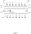
- FIG. 7 depicts example injection of a fluorine containing gas using post-plasma gas injection according to example embodiments of the present disclosure.
- the separation grid 200 includes a first grid plate 210 and a second grid plate 220 disposed in parallel relationship.
- the first grid plate 210 and the second grid plate 220 can provide for ion/UV filtering.
- the first grid plate 210 can have a first grid pattern having a plurality of holes.
- the second grid plate 220 can have a second grid pattern having a plurality of holes.
- the first grid pattern can be the same as or different from the second grid pattern.
- Species 215 from the plasma can be exposed to the separation grid 200 .
- Charged particles e.g., ions
- Neutral species can flow relatively freely through the holes in the first grid plate 210 and the second grid plate 220 .
- a gas injection source 230 can be configured to introduce NF 3 gas or CH 4 gas or other fluorine containing hydrocarbons such as CH 2 F 2 , CHF 3 , CH 3 F into the species passing through the separation grid 200 .
- a mixture 225 can pass through a third grid plate 235 for exposure to the workpiece in the processing chamber.
- the present example is discussed with reference to a separation grid with three grid plates for example purposes. Those of ordinary skill in the art, using the disclosures provided herein, will understand that more or fewer grid plates can be used without deviating from the scope of the present disclosure.
- the NF 3 gas or CH 4 gas or other fluorine containing hydrocarbons such as CH 2 F 2 , CHF 3 , CH 3 F can be mixed with the species at any point in the separation grid and/or after the separation grid in the processing chamber.
- the gas source 230 can be located between first grid plate 210 and second grid plate 220 .
- the plasma etch processes e.g., native oxide punch-through process, silicon mandrel or silicon replacement gate removal process, and spacer open process
- plasma etch processes can be implemented using other plasma processing apparatus without deviating from the scope of the present disclosure.
- the silicon mandrel or silicon replacement gate removal process and native oxide punch through process can be implemented in the same plasma processing apparatus.
- capacitively coupled plasma can be generated in a processing chamber using the same plasma processing apparatus as the plasma processing apparatus used to perform a silicon mandrel or a silicon replacement gate etch.
- a workpiece can include a silicon mandrel or a silicon replacement gate at least partially covered by a native oxide layer. The workpiece can be placed into a processing chamber for silicon mandrel or silicon replacement gate removal process.
- a native oxide punch-through process can be performed by a capacitively coupled plasma induced in the processing chamber to remove the native oxide layer on top of the silicon mandrels or silicon replacement gates.
- an inductively coupled plasma can be used for silicon mandrel or silicon replacement gate removal process.
- FIG. 8 depicts an example plasma processing apparatus 800 that can be used to implement processes according to example embodiments of the present disclosure.
- the plasma processing apparatus 800 is similar to the plasma processing apparatus 100 of FIG. 3 .
- plasma processing apparatus 800 includes a processing chamber 110 and a plasma chamber 120 that is separated from the processing chamber 110 .
- Processing chamber 110 includes a substrate holder or pedestal 112 operable to hold a workpiece 114 to be processed, such as a semiconductor wafer.
- a plasma is generated in plasma chamber 120 (i.e., plasma generation region) by an inductively coupled plasma source 135 and desired species are channeled from the plasma chamber 120 to the surface of substrate 114 through a separation grid assembly 200 .
- the plasma chamber 120 includes a dielectric side wall 122 and a ceiling 124 .
- the dielectric side wall 122 , ceiling 124 , and separation grid 200 define a plasma chamber interior 125 .
- Dielectric side wall 122 can be formed from a dielectric material, such as quartz and/or alumina.
- the inductively coupled plasma source 135 can include an induction coil 130 disposed adjacent the dielectric side wall 122 about the plasma chamber 120 .
- the induction coil 130 is coupled to an RF power generator 134 through a suitable matching network 132 .
- Process gases e.g., an inert gas
- the plasma processing apparatus 100 can include an optional grounded Faraday shield 128 to reduce capacitive coupling of the induction coil 130 to the plasma.
- a separation grid 200 separates the plasma chamber 120 from the processing chamber 110 .
- the separation grid 200 can be used to perform ion filtering from a mixture generated by plasma in the plasma chamber 120 to generate a filtered mixture.
- the filtered mixture can be exposed to the workpiece 114 in the processing chamber.
- the separation grid 200 can be a multi-plate separation grid.
- the separation grid 200 can include a first grid plate 210 and a second grid plate 220 that are spaced apart in parallel relationship to one another.
- the first grid plate 210 and the second grid plate 220 can be separated by a distance.
- the first grid plate 210 can have a first grid pattern having a plurality of holes.
- the second grid plate 220 can have a second grid pattern having a plurality of holes.
- the first grid pattern can be the same as or different from the second grid pattern.
- Charged particles can recombine on the walls in their path through the holes of each grid plate 210 , 220 in the separation grid.
- Neutral species e.g., radicals
- the size of the holes and thickness of each grid plate 210 and 220 can affect transparency for both charged and neutral particles.
- the first grid plate 210 can be made of metal (e.g., aluminum) or other electrically conductive material and/or the second grid plate 220 can be made from either an electrically conductive material or dielectric material (e.g., quartz, ceramic, etc.). In some embodiments, the first grid plate 210 and/or the second grid plate 220 can be made of other materials, such as silicon or silicon carbide. In the event a grid plate is made of metal or other electrically conductive material, the grid plate can be grounded.
- metal e.g., aluminum
- the second grid plate 220 can be made from either an electrically conductive material or dielectric material (e.g., quartz, ceramic, etc.).
- the first grid plate 210 and/or the second grid plate 220 can be made of other materials, such as silicon or silicon carbide. In the event a grid plate is made of metal or other electrically conductive material, the grid plate can be grounded.
- the example plasma processing apparatus 800 of FIG. 8 is operable to generate a first plasma 802 (e.g., a remote plasma) in the plasma chamber 120 and a second plasma 804 (e.g., a direct plasma) in the processing chamber 110 .
- the first plasma 802 can be generated by an inductively coupled plasma source.
- the second plasma 804 can be generated by, for instance, a capacitively coupled plasma source (e.g., bias).
- a “remote plasma” refers to a plasma generated remotely from a workpiece, such as in a plasma chamber separated from a workpiece by a separation grid.
- a “direct plasma” refers to a plasma that is directly exposed to a workpiece, such as a plasma generated in a processing chamber having a pedestal operable to support the workpiece.
- the plasma processing apparatus 800 of FIG. 8 includes a bias source having bias electrode 810 in the pedestal 112 .
- the bias electrode 810 can be coupled to an RF power generator 814 via a suitable matching network 812 .
- a second plasma 804 can be generated from a mixture in the processing chamber 110 for direct exposure to the workpiece 114 .
- the processing chamber 110 can include a gas exhaust port 816 for evacuating a gas from the processing chamber 110 .
- the apparatus 100 can include a gas delivery system 150 configured to deliver process gas to the plasma chamber 120 , for instance, via gas distribution channel 151 or other distribution system (e.g., showerhead).
- the gas delivery system can include a plurality of feed gas lines 159 .
- the feed gas lines 159 can be controlled using valves and/or mass flow controllers to deliver a desired amount of gases into the plasma chamber as process gas. As shown in FIG. 8 , according to example aspects of the present disclosure, the apparatus 100 can include a gas delivery system 150 configured to deliver process gas to the plasma chamber 120 , for instance, via gas distribution channel 151 or other distribution system (e.g., showerhead).
- the gas delivery system can include a plurality of feed gas lines 159 .
- the feed gas lines 159 can be controlled using valves and/or mass flow controllers to deliver a desired amount of gases into the plasma chamber as process gas. As shown in FIG.
- the gas delivery system 150 can include feed gas line(s) for delivery of a NF 3 gas, feed gas line(s) for delivery of a CF 4 gas, feed gas line(s) for delivery of other fluorine containing hydrocarbons such as CH 2 F 2 , CHF 3 , CH 3 F, feed gas line(s) for delivery of a first hydrogen containing gas (e.g., H 2 /He, or hydrogen gas mixed with other inert gas), and/or feed gas line(s) for delivery of a second hydrogen containing gas (e.g., H 2 /Ar, hydrogen gas mixed with other inert gas).
- a first hydrogen containing gas e.g., H 2 /He, or hydrogen gas mixed with other inert gas
- a second hydrogen containing gas e.g., H 2 /Ar, hydrogen gas mixed with other inert gas
- a control valve and/or mass flow controller 158 can be used to control a flow rate of each feed gas line to flow a process gas (e.g., H 2 /He/NF 3 , H 2 /Ar/NF 3 , H 2 /He/CF 4 , or H 2 /Ar/CF 4 ) into the plasma chamber 120 .
- a process gas e.g., H 2 /He/NF 3 , H 2 /Ar/NF 3 , H 2 /He/CF 4 , or H 2 /Ar/CF 4
- the workpiece 114 can include a silicon mandrel or silicon replacement gate at least partially covered by a native oxide layer.
- the workpiece 114 can be placed into the processing chamber 110 for silicon mandrel or silicon replacement gate removal process.
- a native oxide punch-through process can be performed by a capacitively coupled plasma 804 induced via the bias electrode 810 in the processing chamber 110 to remove the native oxide layer on top of the silicon mandrel or silicon replacement gate.
- an inductively coupled plasma 802 in the plasma chamber 120 can be used for etching the silicon mandrel or silicon replacement gate of the workpiece 114 .
Landscapes
- Chemical & Material Sciences (AREA)
- Physics & Mathematics (AREA)
- Engineering & Computer Science (AREA)
- Plasma & Fusion (AREA)
- Analytical Chemistry (AREA)
- Drying Of Semiconductors (AREA)
- Composite Materials (AREA)
- Plasma Technology (AREA)
Abstract
Description
Claims (10)
Priority Applications (1)
| Application Number | Priority Date | Filing Date | Title |
|---|---|---|---|
| US16/716,585 US11387115B2 (en) | 2018-12-20 | 2019-12-17 | Silicon mandrel etch after native oxide punch-through |
Applications Claiming Priority (3)
| Application Number | Priority Date | Filing Date | Title |
|---|---|---|---|
| US201862782653P | 2018-12-20 | 2018-12-20 | |
| US201962790661P | 2019-01-10 | 2019-01-10 | |
| US16/716,585 US11387115B2 (en) | 2018-12-20 | 2019-12-17 | Silicon mandrel etch after native oxide punch-through |
Publications (2)
| Publication Number | Publication Date |
|---|---|
| US20200203182A1 US20200203182A1 (en) | 2020-06-25 |
| US11387115B2 true US11387115B2 (en) | 2022-07-12 |
Family
ID=71097808
Family Applications (1)
| Application Number | Title | Priority Date | Filing Date |
|---|---|---|---|
| US16/716,585 Active US11387115B2 (en) | 2018-12-20 | 2019-12-17 | Silicon mandrel etch after native oxide punch-through |
Country Status (4)
| Country | Link |
|---|---|
| US (1) | US11387115B2 (en) |
| CN (1) | CN112368808B (en) |
| TW (1) | TW202101520A (en) |
| WO (1) | WO2020131793A1 (en) |
Cited By (1)
| Publication number | Priority date | Publication date | Assignee | Title |
|---|---|---|---|---|
| US20220084792A1 (en) * | 2019-07-17 | 2022-03-17 | Mattson Technology, Inc. | Variable mode plasma chamber utilizing tunable plasma potential |
Families Citing this family (3)
| Publication number | Priority date | Publication date | Assignee | Title |
|---|---|---|---|---|
| CN113488367A (en) * | 2020-12-14 | 2021-10-08 | 北京屹唐半导体科技股份有限公司 | Workpiece processing apparatus having a plasma processing system and a thermal processing system |
| CN113471049B (en) | 2021-06-30 | 2022-07-26 | 北京屹唐半导体科技股份有限公司 | Method for processing workpiece, plasma etching machine and semiconductor device |
| TWI829426B (en) * | 2022-11-14 | 2024-01-11 | 力晶積成電子製造股份有限公司 | Multilayer stacking wafer bonding structure and method of manufacturing the same |
Citations (13)
| Publication number | Priority date | Publication date | Assignee | Title |
|---|---|---|---|---|
| US20010001743A1 (en) | 1999-04-20 | 2001-05-24 | Mcreynolds Darrell | Mechanism for etching a silicon layer in a plasma processing chamber to form deep openings |
| US20120091095A1 (en) * | 2010-10-15 | 2012-04-19 | Applied Materials, Inc. | Method and apparatus for reducing particle defects in plasma etch chambers |
| US20120208371A1 (en) * | 2011-02-15 | 2012-08-16 | Applied Materials, Inc. | Method and apparatus for multizone plasma generation |
| US20130089988A1 (en) * | 2011-10-07 | 2013-04-11 | Applied Materials, Inc. | Selective etch of silicon by way of metastable hydrogen termination |
| US20130193108A1 (en) * | 2012-01-27 | 2013-08-01 | Applied Materials, Inc. | Methods of end point detection for substrate fabrication processes |
| US20140248780A1 (en) * | 2013-03-01 | 2014-09-04 | Applied Materials, Inc. | Enhanced etching processes using remote plasma sources |
| US20150079797A1 (en) | 2013-09-16 | 2015-03-19 | Applied Materials, Inc. | Selective etch of silicon nitride |
| US20150187939A1 (en) * | 2013-12-31 | 2015-07-02 | Taiwan Semiconductor Manufacturing Company, Ltd. | Metal Gate Transistor and Method for Tuning Metal Gate Profile |
| US20160064519A1 (en) | 2012-07-02 | 2016-03-03 | Lam Research Corporation | Ultrahigh selective polysilicon etch with high throughput |
| US20160181112A1 (en) * | 2014-12-23 | 2016-06-23 | Applied Materials, Inc. | Anisotropic gap etch |
| US20160276134A1 (en) | 2015-03-17 | 2016-09-22 | Applied Materials, Inc. | Ion-ion plasma atomic layer etch process and reactor |
| US20180358208A1 (en) | 2017-06-09 | 2018-12-13 | Mattson Technology, Inc. | Plasma Processing Apparatus With Post Plasma Gas Injection |
| US20200127013A1 (en) * | 2018-10-23 | 2020-04-23 | Globalfoundries Inc. | Dummy gate isolation and method of production thereof |
Family Cites Families (4)
| Publication number | Priority date | Publication date | Assignee | Title |
|---|---|---|---|---|
| CN102543838B (en) * | 2010-12-22 | 2014-01-29 | 中国科学院微电子研究所 | Method for manufacturing semiconductor device |
| CN102543713B (en) * | 2012-02-28 | 2014-05-28 | 上海华力微电子有限公司 | Method for etching oxide silicon grid compensating isolation region |
| US20140271097A1 (en) * | 2013-03-15 | 2014-09-18 | Applied Materials, Inc. | Processing systems and methods for halide scavenging |
| US9824893B1 (en) * | 2016-06-28 | 2017-11-21 | Lam Research Corporation | Tin oxide thin film spacers in semiconductor device manufacturing |
-
2019
- 2019-12-17 CN CN201980044826.9A patent/CN112368808B/en active Active
- 2019-12-17 US US16/716,585 patent/US11387115B2/en active Active
- 2019-12-17 WO PCT/US2019/066725 patent/WO2020131793A1/en not_active Ceased
- 2019-12-20 TW TW108146982A patent/TW202101520A/en unknown
Patent Citations (14)
| Publication number | Priority date | Publication date | Assignee | Title |
|---|---|---|---|---|
| US20010001743A1 (en) | 1999-04-20 | 2001-05-24 | Mcreynolds Darrell | Mechanism for etching a silicon layer in a plasma processing chamber to form deep openings |
| US20120091095A1 (en) * | 2010-10-15 | 2012-04-19 | Applied Materials, Inc. | Method and apparatus for reducing particle defects in plasma etch chambers |
| US20120208371A1 (en) * | 2011-02-15 | 2012-08-16 | Applied Materials, Inc. | Method and apparatus for multizone plasma generation |
| US20130089988A1 (en) * | 2011-10-07 | 2013-04-11 | Applied Materials, Inc. | Selective etch of silicon by way of metastable hydrogen termination |
| US8808563B2 (en) | 2011-10-07 | 2014-08-19 | Applied Materials, Inc. | Selective etch of silicon by way of metastable hydrogen termination |
| US20130193108A1 (en) * | 2012-01-27 | 2013-08-01 | Applied Materials, Inc. | Methods of end point detection for substrate fabrication processes |
| US20160064519A1 (en) | 2012-07-02 | 2016-03-03 | Lam Research Corporation | Ultrahigh selective polysilicon etch with high throughput |
| US20140248780A1 (en) * | 2013-03-01 | 2014-09-04 | Applied Materials, Inc. | Enhanced etching processes using remote plasma sources |
| US20150079797A1 (en) | 2013-09-16 | 2015-03-19 | Applied Materials, Inc. | Selective etch of silicon nitride |
| US20150187939A1 (en) * | 2013-12-31 | 2015-07-02 | Taiwan Semiconductor Manufacturing Company, Ltd. | Metal Gate Transistor and Method for Tuning Metal Gate Profile |
| US20160181112A1 (en) * | 2014-12-23 | 2016-06-23 | Applied Materials, Inc. | Anisotropic gap etch |
| US20160276134A1 (en) | 2015-03-17 | 2016-09-22 | Applied Materials, Inc. | Ion-ion plasma atomic layer etch process and reactor |
| US20180358208A1 (en) | 2017-06-09 | 2018-12-13 | Mattson Technology, Inc. | Plasma Processing Apparatus With Post Plasma Gas Injection |
| US20200127013A1 (en) * | 2018-10-23 | 2020-04-23 | Globalfoundries Inc. | Dummy gate isolation and method of production thereof |
Non-Patent Citations (1)
| Title |
|---|
| PCT International Search Report and Written Opinion for corresponding PCT Application No. PCT/US2019/066725, dated Apr. 23, 2020, 12 pages. |
Cited By (4)
| Publication number | Priority date | Publication date | Assignee | Title |
|---|---|---|---|---|
| US20220084792A1 (en) * | 2019-07-17 | 2022-03-17 | Mattson Technology, Inc. | Variable mode plasma chamber utilizing tunable plasma potential |
| US12002652B2 (en) * | 2019-07-17 | 2024-06-04 | Mattson Technology, Inc. | Variable mode plasma chamber utilizing tunable plasma potential |
| US20240297019A1 (en) * | 2019-07-17 | 2024-09-05 | Beijing E-town Semiconductor Technology Co., Ltd. | Variable Mode Plasma Chamber Utilizing Tunable Plasma Potential |
| US12562342B2 (en) * | 2019-07-17 | 2026-02-24 | Beijing E-town Semiconductor Technology Co., Ltd. | Variable mode plasma chamber utilizing tunable plasma potential |
Also Published As
| Publication number | Publication date |
|---|---|
| TW202101520A (en) | 2021-01-01 |
| WO2020131793A1 (en) | 2020-06-25 |
| CN112368808B (en) | 2025-03-14 |
| US20200203182A1 (en) | 2020-06-25 |
| CN112368808A (en) | 2021-02-12 |
Similar Documents
| Publication | Publication Date | Title |
|---|---|---|
| US11387115B2 (en) | Silicon mandrel etch after native oxide punch-through | |
| US20200135554A1 (en) | Water Vapor Based Fluorine Containing Plasma For Removal Of Hardmask | |
| US11276560B2 (en) | Spacer etching process | |
| US11387111B2 (en) | Processing of workpieces with reactive species generated using alkyl halide | |
| US11495437B2 (en) | Surface pretreatment process to improve quality of oxide films produced by remote plasma | |
| US11195718B2 (en) | Spacer open process by dual plasma | |
| US11791166B2 (en) | Selective etch process using hydrofluoric acid and ozone gases | |
| US11651977B2 (en) | Processing of workpieces using fluorocarbon plasma | |
| WO2022046615A1 (en) | Plasma strip tool with movable insert | |
| US10872761B2 (en) | Post etch defluorination process | |
| US11043393B2 (en) | Ozone treatment for selective silicon nitride etch over silicon | |
| US11257680B2 (en) | Methods for processing a workpiece using fluorine radicals | |
| US20210391185A1 (en) | Surface Smoothing of Workpieces | |
| US20210202231A1 (en) | Systems and Methods for Removal of Hardmask | |
| US11164727B2 (en) | Processing of workpieces using hydrogen radicals and ozone gas |
Legal Events
| Date | Code | Title | Description |
|---|---|---|---|
| FEPP | Fee payment procedure |
Free format text: ENTITY STATUS SET TO UNDISCOUNTED (ORIGINAL EVENT CODE: BIG.); ENTITY STATUS OF PATENT OWNER: LARGE ENTITY |
|
| AS | Assignment |
Owner name: BEIJING E-TOWN SEMICONDUCTOR TECHNOLOGY, CO., LTD, CHINA Free format text: ASSIGNMENT OF ASSIGNORS INTEREST;ASSIGNOR:MATTSON TECHNOLOGY, INC.;REEL/FRAME:051319/0279 Effective date: 20190925 Owner name: MATTSON TECHNOLOGY, INC., CALIFORNIA Free format text: ASSIGNMENT OF ASSIGNORS INTEREST;ASSIGNOR:MATTSON TECHNOLOGY, INC.;REEL/FRAME:051319/0279 Effective date: 20190925 Owner name: MATTSON TECHNOLOGY, INC., CALIFORNIA Free format text: ASSIGNMENT OF ASSIGNORS INTEREST;ASSIGNORS:YAN, CHUN;SUNG, TSAI WEN;LO, SIO ON;AND OTHERS;SIGNING DATES FROM 20190128 TO 20190206;REEL/FRAME:051319/0157 |
|
| STPP | Information on status: patent application and granting procedure in general |
Free format text: DOCKETED NEW CASE - READY FOR EXAMINATION |
|
| AS | Assignment |
Owner name: EAST WEST BANK, CALIFORNIA Free format text: SECURITY INTEREST;ASSIGNOR:MATTSON TECHNOLOGY, INC.;REEL/FRAME:054100/0167 Effective date: 20180821 |
|
| STPP | Information on status: patent application and granting procedure in general |
Free format text: NON FINAL ACTION MAILED |
|
| STPP | Information on status: patent application and granting procedure in general |
Free format text: RESPONSE TO NON-FINAL OFFICE ACTION ENTERED AND FORWARDED TO EXAMINER |
|
| AS | Assignment |
Owner name: MATTSON TECHNOLOGY, INC., CALIFORNIA Free format text: RELEASE BY SECURED PARTY;ASSIGNOR:EAST WEST BANK;REEL/FRAME:055950/0452 Effective date: 20210415 Owner name: MATTSON TECHNOLOGY, INC., CALIFORNIA Free format text: RELEASE OF SECURITY INTEREST;ASSIGNOR:EAST WEST BANK;REEL/FRAME:055950/0452 Effective date: 20210415 |
|
| STPP | Information on status: patent application and granting procedure in general |
Free format text: FINAL REJECTION MAILED |
|
| STPP | Information on status: patent application and granting procedure in general |
Free format text: RESPONSE AFTER FINAL ACTION FORWARDED TO EXAMINER |
|
| STPP | Information on status: patent application and granting procedure in general |
Free format text: ADVISORY ACTION MAILED |
|
| STPP | Information on status: patent application and granting procedure in general |
Free format text: DOCKETED NEW CASE - READY FOR EXAMINATION |
|
| STPP | Information on status: patent application and granting procedure in general |
Free format text: NON FINAL ACTION MAILED |
|
| STPP | Information on status: patent application and granting procedure in general |
Free format text: RESPONSE TO NON-FINAL OFFICE ACTION ENTERED AND FORWARDED TO EXAMINER |
|
| STPP | Information on status: patent application and granting procedure in general |
Free format text: NOTICE OF ALLOWANCE MAILED -- APPLICATION RECEIVED IN OFFICE OF PUBLICATIONS |
|
| STPP | Information on status: patent application and granting procedure in general |
Free format text: PUBLICATIONS -- ISSUE FEE PAYMENT RECEIVED |
|
| STCF | Information on status: patent grant |
Free format text: PATENTED CASE |
|
| MAFP | Maintenance fee payment |
Free format text: PAYMENT OF MAINTENANCE FEE, 4TH YEAR, LARGE ENTITY (ORIGINAL EVENT CODE: M1551); ENTITY STATUS OF PATENT OWNER: LARGE ENTITY Year of fee payment: 4 |