US11373899B2 - Pattern generation device, pattern generation method, and method of manufacturing semiconductor device - Google Patents
Pattern generation device, pattern generation method, and method of manufacturing semiconductor device Download PDFInfo
- Publication number
- US11373899B2 US11373899B2 US16/808,467 US202016808467A US11373899B2 US 11373899 B2 US11373899 B2 US 11373899B2 US 202016808467 A US202016808467 A US 202016808467A US 11373899 B2 US11373899 B2 US 11373899B2
- Authority
- US
- United States
- Prior art keywords
- mask
- function
- integral kernel
- pattern
- misalignment
- Prior art date
- Legal status (The legal status is an assumption and is not a legal conclusion. Google has not performed a legal analysis and makes no representation as to the accuracy of the status listed.)
- Active, expires
Links
Images


Classifications
-
- H—ELECTRICITY
- H01—ELECTRIC ELEMENTS
- H01L—SEMICONDUCTOR DEVICES NOT COVERED BY CLASS H10
- H01L21/00—Processes or apparatus adapted for the manufacture or treatment of semiconductor or solid state devices or of parts thereof
- H01L21/70—Manufacture or treatment of devices consisting of a plurality of solid state components formed in or on a common substrate or of parts thereof; Manufacture of integrated circuit devices or of parts thereof
- H01L21/71—Manufacture of specific parts of devices defined in group H01L21/70
- H01L21/768—Applying interconnections to be used for carrying current between separate components within a device comprising conductors and dielectrics
- H01L21/76801—Applying interconnections to be used for carrying current between separate components within a device comprising conductors and dielectrics characterised by the formation and the after-treatment of the dielectrics, e.g. smoothing
- H01L21/76802—Applying interconnections to be used for carrying current between separate components within a device comprising conductors and dielectrics characterised by the formation and the after-treatment of the dielectrics, e.g. smoothing by forming openings in dielectrics
-
- G—PHYSICS
- G03—PHOTOGRAPHY; CINEMATOGRAPHY; ANALOGOUS TECHNIQUES USING WAVES OTHER THAN OPTICAL WAVES; ELECTROGRAPHY; HOLOGRAPHY
- G03F—PHOTOMECHANICAL PRODUCTION OF TEXTURED OR PATTERNED SURFACES, e.g. FOR PRINTING, FOR PROCESSING OF SEMICONDUCTOR DEVICES; MATERIALS THEREFOR; ORIGINALS THEREFOR; APPARATUS SPECIALLY ADAPTED THEREFOR
- G03F1/00—Originals for photomechanical production of textured or patterned surfaces, e.g., masks, photo-masks, reticles; Mask blanks or pellicles therefor; Containers specially adapted therefor; Preparation thereof
- G03F1/68—Preparation processes not covered by groups G03F1/20 - G03F1/50
- G03F1/70—Adapting basic layout or design of masks to lithographic process requirements, e.g., second iteration correction of mask patterns for imaging
-
- H10W20/081—
-
- G—PHYSICS
- G03—PHOTOGRAPHY; CINEMATOGRAPHY; ANALOGOUS TECHNIQUES USING WAVES OTHER THAN OPTICAL WAVES; ELECTROGRAPHY; HOLOGRAPHY
- G03F—PHOTOMECHANICAL PRODUCTION OF TEXTURED OR PATTERNED SURFACES, e.g. FOR PRINTING, FOR PROCESSING OF SEMICONDUCTOR DEVICES; MATERIALS THEREFOR; ORIGINALS THEREFOR; APPARATUS SPECIALLY ADAPTED THEREFOR
- G03F7/00—Photomechanical, e.g. photolithographic, production of textured or patterned surfaces, e.g. printing surfaces; Materials therefor, e.g. comprising photoresists; Apparatus specially adapted therefor
- G03F7/70—Microphotolithographic exposure; Apparatus therefor
- G03F7/70483—Information management; Active and passive control; Testing; Wafer monitoring, e.g. pattern monitoring
- G03F7/70605—Workpiece metrology
- G03F7/70616—Monitoring the printed patterns
-
- G—PHYSICS
- G06—COMPUTING OR CALCULATING; COUNTING
- G06F—ELECTRIC DIGITAL DATA PROCESSING
- G06F30/00—Computer-aided design [CAD]
- G06F30/30—Circuit design
- G06F30/39—Circuit design at the physical level
- G06F30/392—Floor-planning or layout, e.g. partitioning or placement
-
- H—ELECTRICITY
- H01—ELECTRIC ELEMENTS
- H01L—SEMICONDUCTOR DEVICES NOT COVERED BY CLASS H10
- H01L21/00—Processes or apparatus adapted for the manufacture or treatment of semiconductor or solid state devices or of parts thereof
- H01L21/70—Manufacture or treatment of devices consisting of a plurality of solid state components formed in or on a common substrate or of parts thereof; Manufacture of integrated circuit devices or of parts thereof
- H01L21/71—Manufacture of specific parts of devices defined in group H01L21/70
- H01L21/768—Applying interconnections to be used for carrying current between separate components within a device comprising conductors and dielectrics
- H01L21/76898—Applying interconnections to be used for carrying current between separate components within a device comprising conductors and dielectrics formed through a semiconductor substrate
-
- H01L27/0207—
-
- H01L29/7845—
-
- H—ELECTRICITY
- H10—SEMICONDUCTOR DEVICES; ELECTRIC SOLID-STATE DEVICES NOT OTHERWISE PROVIDED FOR
- H10D—INORGANIC ELECTRIC SEMICONDUCTOR DEVICES
- H10D30/00—Field-effect transistors [FET]
- H10D30/60—Insulated-gate field-effect transistors [IGFET]
- H10D30/791—Arrangements for exerting mechanical stress on the crystal lattice of the channel regions
- H10D30/794—Arrangements for exerting mechanical stress on the crystal lattice of the channel regions comprising conductive materials, e.g. silicided source, drain or gate electrodes
-
- H—ELECTRICITY
- H10—SEMICONDUCTOR DEVICES; ELECTRIC SOLID-STATE DEVICES NOT OTHERWISE PROVIDED FOR
- H10D—INORGANIC ELECTRIC SEMICONDUCTOR DEVICES
- H10D89/00—Aspects of integrated devices not covered by groups H10D84/00 - H10D88/00
- H10D89/10—Integrated device layouts
-
- H10W20/023—
-
- G—PHYSICS
- G06—COMPUTING OR CALCULATING; COUNTING
- G06F—ELECTRIC DIGITAL DATA PROCESSING
- G06F30/00—Computer-aided design [CAD]
- G06F30/30—Circuit design
- G06F30/39—Circuit design at the physical level
- G06F30/398—Design verification or optimisation, e.g. using design rule check [DRC], layout versus schematics [LVS] or finite element methods [FEM]
Definitions
- the present disclosure embodiments relate to a pattern generation device, a pattern generation method and a method of manufacturing semiconductor device.
- the manufacturing process of a semiconductor device includes a process of stacking layers made of a plurality of different materials. Various hole patterns are formed by an exposure process in these layers. These patterns should be aligned with the underlying patterns. However, when a plurality of layers made of different materials is stacked, a membrane stress is generated, resulting in a misalignment of patterns. In addition, the misalignment of patterns is also caused by stress generated in the joint surface of different materials. Therefore, for such misalignment of a pattern, (1) a method of correcting the mask pattern by obtaining the position displacement amount with reference to the measured value, and (2) a method of correcting the mask pattern by calculating the stress by simulations and predicting the misalignment value, have been proposed.
- FIG. 1 is a configuration diagram illustrating a pattern generation device according to an embodiment of the present disclosure
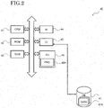
- FIG. 2 is a configuration diagram illustrating a system incorporating the pattern generation device according to an embodiment of the present disclosure
- FIG. 3A and FIG. 3B are diagrams illustrating a misalignment between a upper layer and a lower layer in a semiconductor device according to an embodiment of the present disclosure
- FIGS. 4A, 4B, 4C and 4D are diagrams illustrating a process of calculating a misalignment value caused by stress from layout information in the pattern generation method according to an embodiment of the present disclosure
- FIGS. 6A, 6B, 6C, 6D, 6E, 6F, 6G and 6H are diagrams illustrating the graphs of the integral kernel in Fourier space and real space used in an embodiment of the present disclosure
- FIGS. 7A, 7B, 7C, 7D and 7E are diagrams illustrating a result of convolution of a mask function and the integral kernel used in an embodiment of the present disclosure
- FIGS. 8A, 8B and 8C are diagrams illustrating an example of the mask function and the integral kernel in Fourier space used in an embodiment of the present disclosure
- FIG. 9A and FIG. 9B are diagrams illustrating how patterns are generated by the pattern generation method used in an embodiment of the present disclosure.
- FIG. 10A and FIG. 10B are diagrams illustrating how patterns are generated by the pattern generation method used in an embodiment of the present disclosure.
- FIG. 11 is a diagram illustrating a comparison between a graph of misalignment value calculated by the pattern generation method used in an embodiment of the present disclosure and a misalignment value measured using a cross sectional SEM.
- a pattern generation device includes a misalignment value calculation unit and a pattern correction unit.
- the misalignment value calculation unit acquires a layout information, calculates a layout function from the layout information, and calculates a misalignment value by a convolution of the layout function and an integral kernel having a predetermined parameter.
- the pattern correction unit corrects a pattern to generate a modified layout information using a calculated result by the misalignment value calculation unit, and output the modified layout information.
- FIG. 1 shows a pattern generation device 1 according to an embodiment of the present disclosure.
- the pattern generation device 1 comprises a misalignment value calculation unit 10 and a mask pattern correction unit 30 . Both are implemented as a computer program in a computer system as shown in FIG. 2 .
- the misalignment value calculation unit 10 acquires a layout information 11 defining a plurality of areas in which characteristic misalignment occurs by stress and calculates a layout function from the layout information 11 (step 12 ). Since the pattern is two-dimensional, the layout function is a function with two arguments, x and y, indicating the position on the plane. In the following examples of a semiconductor device, the layout function can be 1 in the region B of the semiconductor device and 0 in the region A of the semiconductor device. However, the layout function is not limited to this and may set any values that differ from region to region.
- the misalignment value calculation unit 10 calculates a misalignment value corresponding to the layouts (step 14 ).
- the misalignment value is calculated by convolution of the layout function and the integral kernel, which will be described later.
- the misalignment value is output in a map format binary data or an ASCII.
- the mask pattern correction unit 30 performs correction of the patterns using the calculation results obtained in the misalignment value calculation unit 10 .
- the mask pattern correction unit 30 receives the original data in the GDS format, performs correction using misalignment value, and outputs the corrected data in the GDS format as a mask pattern.
- the pattern generation device 1 (pattern generation method) according to an embodiment of the present disclosure is implemented as a computer program in a computer system 40 as shown in FIG. 2 .
- the computer system 40 includes a system terminal having a CPU 41 , ROM 42 , RAM 43 , human interface (HI) 44 , communication interface (CI) 45 , and storage device (SD) 46 connected by a bus, and a database (DB) 47 connected to the system terminal through the communication interface (CI) 45 by a network.
- the layout information 11 , the pattern misalignment value measured at each individual attention points, and original data of the mask pattern are stored in a predetermined area 47 A of the database (DB) 47 .
- the steps of calculating the layout function (step 12 ), estimating the parameters of the integral kernel by fitting to the measured data (step 13 ), and calculating the misalignment value corresponding to the layout (step 14 ) are all implemented as a program module, which is stored in a predetermined area 46 A of the storage device (SD) 46 .
- the mask pattern correction unit 30 for performing the mask pattern correction is also implemented as a program module, which is stored in a predetermined area 46 A of the storage device (SD) 46 .
- the pattern generation device/pattern generation method is configured as described above.
- the misalignment value is expressed as a convolutional integral of the layout function and integral kernel, which is less calculation and makes it feasible to correct the entire surface of semiconductor chips, which was impossible with a rigorous stress simulation with a large amount of calculation.
- FIG. 3A and FIG. 3B are diagrams illustrating a cross section of a semiconductor device according to an embodiment of the present disclosure.
- the semiconductor device 50 is a semiconductor chip.
- the construction of the semiconductor device 50 is referred to as a layout information.
- FIG. 3A and FIG. 3B a region A and a region B in the semiconductor device 50 are shown.
- FIG. 3A shows a cross-section of the region A and the region B including Upper Layer (UL) and Lower Layer (LL).
- the region A and the region B are the unit regions that can be approximated as homogeneous different materials in the stress calculations of upper layer (UL).
- FIG. 3B is a diagram showing an example in which a misalignment occurs between the electrode 51 (e.g., memory hole, via hole) of the upper layer (UL) and the electrode 52 (e.g., wiring, diffusion layer) of the lower layer (LL) in the semiconductor device.
- the electrode 51 e.g., memory hole, via hole
- the electrode 52 e.g., wiring, diffusion layer
- the electric resistance between the electrode 52 formed in the lower layer (LL) and the electrode 51 formed in the upper layer (UL) increases. Further, if the position is excessively shifted, it is possible to lead a disconnection of the upper-layer electrode 51 and the lower-layer electrode 52 . This is a reason for reducing the yield of the semiconductor device, so that the correction of the mask pattern is needed.
- FIGS. 4A, 4B, 4C and 4D are diagrams illustrating a process of calculating a misalignment value caused by stress from the layout information as shown in FIG. 3A and FIG. 3B in a pattern generation method according to an embodiment of the present disclosure.
- the process is to express the phenomena that the misalignment value is relaxed in proportion to the distance from the position where the stress is concentrated by the formula, the position where the stress is concentrated is obtained from the layout information, and the relaxation value is obtained from the measured value.
- FIG. 4A shows an layout function. From the layout information, it is possible to calculate (extract) the information of the plurality of regions in which characteristic misalignment are caused by stress, as a layout function. For example, from the layout information of FIG. 3A and FIG. 3B , it is possible to calculate (extract) a layout function that takes a value of 0 in the region A and a value of 1 in the region B. By differentiating this layout function, as shown in FIG. 4B , the position where the stress is concentrated (before relaxation) is specified. That is, by differentiating the layout function, as shown in FIG. 4B , a stress distribution in which the stress is focused in an impulse shape and distributed in the region boundary can be obtained.
- Integral kernel includes a “first integral kernel” defined by ik/
- the parameter n (relaxation coefficient) is obtained by fitting it to the measured value.
- the misalignment value is calculated by the convolution of the layout function and the first integral kernel, which also represented by functions.
- FIG. 5A is a diagram showing the definitions of the first integral kernel and FIGS. 5B, 5C, 5D and 5E are the graphs of its functions in Fourier space and real space used in an embodiment of the present disclosure.
- FIG. 5A shows the definitions of the first integral kernel. The graphs of the functions are shown in FIG. 5B and FIG. 5C when the parameter n (relaxation coefficient) is 0.
- FIG. 5B is the graphs in Fourier space
- FIG. 5C is the graphs in real space.
- FIG. 5D is the graph in the Fourier space
- FIG. 5E is the graph in the real space.
- FIGS. 6A, 6B, 6C, 6D, 6E, 6F, 6G and 6H show the graphs of the first integral kernel when the parameter n (relaxation coefficient) is changed to 0, 0.5, 0.8, 1.0 in Fourier space and real space.
- FIG. 6A , FIG. 6C , FIG. 6E , and FIG. 6G show the graphs of functions in Fourier space
- FIG. 6B , FIG. 6D , FIG. 6F , and FIG. 6H show the graphs of functions in real space.
- the relaxation value can be easily adjusted by parameter n (relaxation coefficient) by defining the integral kernel in Fourier space with ik/
- FIGS. 7B, 7C, 7D and 7E show the result of convolution of layout function ( FIG. 7A Mask function) and the first integral kernel.
- the pattern is represented on a two-dimensional plane.
- the layout function (Mask function) also has two-dimensional variables x and y.
- the misalignment value is also represented by a two-dimensional vector at this position.
- misalignment value is also a function with two-dimensional vector quantities.
- FIG. 4 to FIG. 7 are presented in one-dimensional form for ease of understanding.
- the integral kernel described above further includes a Gaussian function defined as exp( ⁇ 2 k 2 /2) in the Fourier space.
- the misalignment value can also be calculated by the convolution of a second integral kernel and the layout function (Mask Function).
- the second integral kernel includes the product of the Gaussian function and the first integral kernel.
- FIGS. 8A, 8B and 8C show the formula.
- FIG. 8A shows layout function (Mask Function). Real space denotes m(x) and Fourier space denotes M(k).
- the integral kernel (kernel(k)) convoluted with this layout function is expressed as the product of Gaussian function and the first integral kernel described above in the Fourier space.
- the second integral kernel (kernel(k)) is expressed as a linear combination of the product of the Gaussian function and the first integral kernel. Note that the parameter a of the Gaussian function is also set as appropriate by fitting to the measured value.
- FIG. 9 and FIG. 10 show how the patterns are generated by the pattern generation method used in an embodiment of the present disclosure.
- FIG. 9A shows a layout function (Mask Function). Region B (denoted B in the figure) has a value of 1 and the other region A has a value of 0.
- FIG. 9B shows the result of the convolution of the layout function (Mask Function) in FIG. 9 A and the Gaussian function defined by exp( ⁇ 2 k 2 /2) in the real space. The transition region from 1 to 0 is indicated with a gradient effect.
- FIG. 10A shows the result of the convolution of the second integral kernel and the layout function (Mask Function) in FIG. 9A .
- the second integral kernel includes the linear combination of ik/
- the white line region 101 and the black line region 102 in the diagram are the concentric regions of the stress. These stress intensive regions correspond to the boundaries between region B and region A. In addition, these stress intensive regions correspond to the points where the material or density changes when the regions are approximated as having a single material or density, respectively.
- FIG. 10B is one-dimensional graphical representation of stress values on the lines indicated by arrows in FIG. 10A .
- FIG. 11 is a graph in which the misalignment value calculated by the conventional method (dotted line) and the misalignment value calculated by the method of the embodiment (solid line) in the region B are displayed together.
- the conventional method is the rigorous stress calculation by the TCAD.
- the reason for the difference between the measured value and the calculated value in the conventional method is that the conventional method requires a large amount of calculation, so it is substantially impossible to carry out the so-called fitting operation sufficiently, in which the calculation conditions are changed multiple times so that the difference with the measured value becomes small.
- the calculational amount of the method according to the embodiment of the present disclosure is significantly smaller than that of the conventional method, the difference with the measured value was improved compared with the conventional method because the fitting operation is easy.
- the misalignment can be appropriately corrected. This helps to improve the yield in the semiconductor device and leads to an increase in the capacity of memory cells that can be used effectively.
- the present disclosure can be used for NAND flash memory and 3D memories other than NAND flash memory.
- the present disclosure can also be used for logic devices.
Landscapes
- Engineering & Computer Science (AREA)
- Physics & Mathematics (AREA)
- General Physics & Mathematics (AREA)
- Computer Hardware Design (AREA)
- Theoretical Computer Science (AREA)
- General Engineering & Computer Science (AREA)
- Evolutionary Computation (AREA)
- Geometry (AREA)
- Architecture (AREA)
- Condensed Matter Physics & Semiconductors (AREA)
- Manufacturing & Machinery (AREA)
- Microelectronics & Electronic Packaging (AREA)
- Power Engineering (AREA)
- Preparing Plates And Mask In Photomechanical Process (AREA)
- Chemical & Material Sciences (AREA)
- Materials Engineering (AREA)
- Exposure And Positioning Against Photoresist Photosensitive Materials (AREA)
Abstract
Description
Claims (5)
Applications Claiming Priority (3)
| Application Number | Priority Date | Filing Date | Title |
|---|---|---|---|
| JP2019104838A JP2020197667A (en) | 2019-06-04 | 2019-06-04 | Pattern generator, pattern generation method and manufacturing method of semiconductor device |
| JP2019-104838 | 2019-06-04 | ||
| JPJP2019-104838 | 2019-06-04 |
Publications (2)
| Publication Number | Publication Date |
|---|---|
| US20200388528A1 US20200388528A1 (en) | 2020-12-10 |
| US11373899B2 true US11373899B2 (en) | 2022-06-28 |
Family
ID=73648060
Family Applications (1)
| Application Number | Title | Priority Date | Filing Date |
|---|---|---|---|
| US16/808,467 Active 2040-06-09 US11373899B2 (en) | 2019-06-04 | 2020-03-04 | Pattern generation device, pattern generation method, and method of manufacturing semiconductor device |
Country Status (2)
| Country | Link |
|---|---|
| US (1) | US11373899B2 (en) |
| JP (1) | JP2020197667A (en) |
Citations (6)
| Publication number | Priority date | Publication date | Assignee | Title |
|---|---|---|---|---|
| JPH09326349A (en) * | 1996-06-06 | 1997-12-16 | Hitachi Ltd | Pattern exposure correction method |
| US6548312B1 (en) * | 1999-08-27 | 2003-04-15 | Hitachi, Ltd. | Manufacturing method of semiconductor integrated circuit devices and mask manufacturing methods |
| JP2006058452A (en) * | 2004-08-18 | 2006-03-02 | Toshiba Corp | Mask pattern correction method, mask pattern correction program, photomask manufacturing method, and semiconductor device manufacturing method |
| US8362622B2 (en) | 2009-04-24 | 2013-01-29 | Synopsys, Inc. | Method and apparatus for placing transistors in proximity to through-silicon vias |
| US20180034241A1 (en) | 2016-07-29 | 2018-02-01 | Raytheon Canada Ltd. | Pulse-width modulation light source drive and method |
| US9886542B2 (en) * | 2014-08-04 | 2018-02-06 | E-System Design, Inc. | Modeling TSV interposer considering depletion capacitance and substrate effects |
-
2019
- 2019-06-04 JP JP2019104838A patent/JP2020197667A/en active Pending
-
2020
- 2020-03-04 US US16/808,467 patent/US11373899B2/en active Active
Patent Citations (6)
| Publication number | Priority date | Publication date | Assignee | Title |
|---|---|---|---|---|
| JPH09326349A (en) * | 1996-06-06 | 1997-12-16 | Hitachi Ltd | Pattern exposure correction method |
| US6548312B1 (en) * | 1999-08-27 | 2003-04-15 | Hitachi, Ltd. | Manufacturing method of semiconductor integrated circuit devices and mask manufacturing methods |
| JP2006058452A (en) * | 2004-08-18 | 2006-03-02 | Toshiba Corp | Mask pattern correction method, mask pattern correction program, photomask manufacturing method, and semiconductor device manufacturing method |
| US8362622B2 (en) | 2009-04-24 | 2013-01-29 | Synopsys, Inc. | Method and apparatus for placing transistors in proximity to through-silicon vias |
| US9886542B2 (en) * | 2014-08-04 | 2018-02-06 | E-System Design, Inc. | Modeling TSV interposer considering depletion capacitance and substrate effects |
| US20180034241A1 (en) | 2016-07-29 | 2018-02-01 | Raytheon Canada Ltd. | Pulse-width modulation light source drive and method |
Non-Patent Citations (1)
| Title |
|---|
| Stobert et al., "Model-Based correction for local stress-induced overlay errors", Globalfounderies Inc., Proceedings of SPIE, vol. 10587, 2018, 12 pages. |
Also Published As
| Publication number | Publication date |
|---|---|
| US20200388528A1 (en) | 2020-12-10 |
| JP2020197667A (en) | 2020-12-10 |
Similar Documents
| Publication | Publication Date | Title |
|---|---|---|
| US11922307B2 (en) | Learning device, inference device, and learned model | |
| US11726402B2 (en) | Method and system for layout enhancement based on inter-cell correlation | |
| CN104915528B (en) | Integrated circuit layout design method, layout design system and manufacturing method | |
| US8020121B2 (en) | Layout method and layout apparatus for semiconductor integrated circuit | |
| CN100585604C (en) | Method of Changing Physical Layout Data Using Virtual Layer | |
| US20150227671A1 (en) | Method For Integrated Circuit Mask Patterning | |
| US9672611B2 (en) | Pattern analysis method of a semiconductor device | |
| CN102385242A (en) | Method and system for manufacturing mask | |
| US20080276215A1 (en) | Mask Pattern Designing Method Using Optical Proximity Correction in Optical Lithography, Designing Device, and Semiconductor Device Manufacturing Method Using the Same | |
| TW201717075A (en) | Method and system for adjusting circuit symbols | |
| WO2022058264A1 (en) | Defect detection for semiconductor structures on a wafer | |
| KR20200049373A (en) | System and method for calibrating simulation model | |
| JP2013073139A (en) | Mask layout division method, mask layout division device and mask layout division program | |
| CN107958112B (en) | Edge redundant graph generation method for simulating internal layout graph | |
| TW201523309A (en) | Method for designing semiconductor device, method for preparing integrated circuit device layout, and computer readable storage medium | |
| US11373899B2 (en) | Pattern generation device, pattern generation method, and method of manufacturing semiconductor device | |
| TW201905740A (en) | Method for calculating leakage at the edge of a unit | |
| US20090171644A1 (en) | Ca resistance variability prediction methodology | |
| CN114330207B (en) | Chip pad information extraction method, system and electronic device | |
| CN111367148B (en) | Optical proximity correction method for curve pattern | |
| US7146035B2 (en) | Pattern image comparison method, pattern image comparison device, and program | |
| CN101290904A (en) | Method for correcting layout design for correcting metallic coating of contact hole | |
| CN1983600A (en) | Semiconductor circuit device and design method therefor | |
| JP5141028B2 (en) | Mask layout data creation method, mask layout data creation apparatus, and semiconductor device manufacturing method | |
| US8930171B2 (en) | Method of modeling spatial correlations among integrated circuits with randomly generated spatial frequencies |
Legal Events
| Date | Code | Title | Description |
|---|---|---|---|
| AS | Assignment |
Owner name: KIOXIA CORPORATION, JAPAN Free format text: ASSIGNMENT OF ASSIGNORS INTEREST;ASSIGNORS:KIMURA, TAIKI;MATSUNAWA, TETSUAKI;REEL/FRAME:052004/0599 Effective date: 20200203 |
|
| FEPP | Fee payment procedure |
Free format text: ENTITY STATUS SET TO UNDISCOUNTED (ORIGINAL EVENT CODE: BIG.); ENTITY STATUS OF PATENT OWNER: LARGE ENTITY |
|
| STPP | Information on status: patent application and granting procedure in general |
Free format text: DOCKETED NEW CASE - READY FOR EXAMINATION |
|
| STPP | Information on status: patent application and granting procedure in general |
Free format text: NON FINAL ACTION MAILED |
|
| STPP | Information on status: patent application and granting procedure in general |
Free format text: NOTICE OF ALLOWANCE MAILED -- APPLICATION RECEIVED IN OFFICE OF PUBLICATIONS |
|
| STPP | Information on status: patent application and granting procedure in general |
Free format text: PUBLICATIONS -- ISSUE FEE PAYMENT VERIFIED |
|
| STCF | Information on status: patent grant |
Free format text: PATENTED CASE |
|
| MAFP | Maintenance fee payment |
Free format text: PAYMENT OF MAINTENANCE FEE, 4TH YEAR, LARGE ENTITY (ORIGINAL EVENT CODE: M1551); ENTITY STATUS OF PATENT OWNER: LARGE ENTITY Year of fee payment: 4 |