US11368673B2 - Device designed for detecting a soiling of at least one transmitting window and/or one receiving window of a sensor - Google Patents
Device designed for detecting a soiling of at least one transmitting window and/or one receiving window of a sensor Download PDFInfo
- Publication number
- US11368673B2 US11368673B2 US17/043,104 US201917043104A US11368673B2 US 11368673 B2 US11368673 B2 US 11368673B2 US 201917043104 A US201917043104 A US 201917043104A US 11368673 B2 US11368673 B2 US 11368673B2
- Authority
- US
- United States
- Prior art keywords
- transparent cover
- light beams
- image sensor
- sensor
- hologram structure
- Prior art date
- Legal status (The legal status is an assumption and is not a legal conclusion. Google has not performed a legal analysis and makes no representation as to the accuracy of the status listed.)
- Expired - Fee Related, expires
Links
Images



Classifications
-
- G—PHYSICS
- G01—MEASURING; TESTING
- G01N—INVESTIGATING OR ANALYSING MATERIALS BY DETERMINING THEIR CHEMICAL OR PHYSICAL PROPERTIES
- G01N21/00—Investigating or analysing materials by the use of optical means, i.e. using sub-millimetre waves, infrared, visible or ultraviolet light
- G01N21/84—Systems specially adapted for particular applications
- G01N21/88—Investigating the presence of flaws or contamination
- G01N21/94—Investigating contamination, e.g. dust
-
- H—ELECTRICITY
- H04—ELECTRIC COMMUNICATION TECHNIQUE
- H04N—PICTORIAL COMMUNICATION, e.g. TELEVISION
- H04N17/00—Diagnosis, testing or measuring for television systems or their details
- H04N17/002—Diagnosis, testing or measuring for television systems or their details for television cameras
-
- G—PHYSICS
- G01—MEASURING; TESTING
- G01C—MEASURING DISTANCES, LEVELS OR BEARINGS; SURVEYING; NAVIGATION; GYROSCOPIC INSTRUMENTS; PHOTOGRAMMETRY OR VIDEOGRAMMETRY
- G01C3/00—Measuring distances in line of sight; Optical rangefinders
- G01C3/02—Details
-
- G—PHYSICS
- G01—MEASURING; TESTING
- G01N—INVESTIGATING OR ANALYSING MATERIALS BY DETERMINING THEIR CHEMICAL OR PHYSICAL PROPERTIES
- G01N21/00—Investigating or analysing materials by the use of optical means, i.e. using sub-millimetre waves, infrared, visible or ultraviolet light
- G01N21/01—Arrangements or apparatus for facilitating the optical investigation
- G01N21/15—Preventing contamination of the components of the optical system or obstruction of the light path
-
- G—PHYSICS
- G01—MEASURING; TESTING
- G01S—RADIO DIRECTION-FINDING; RADIO NAVIGATION; DETERMINING DISTANCE OR VELOCITY BY USE OF RADIO WAVES; LOCATING OR PRESENCE-DETECTING BY USE OF THE REFLECTION OR RERADIATION OF RADIO WAVES; ANALOGOUS ARRANGEMENTS USING OTHER WAVES
- G01S17/00—Systems using the reflection or reradiation of electromagnetic waves other than radio waves, e.g. lidar systems
- G01S17/88—Lidar systems specially adapted for specific applications
- G01S17/93—Lidar systems specially adapted for specific applications for anti-collision purposes
- G01S17/931—Lidar systems specially adapted for specific applications for anti-collision purposes of land vehicles
-
- G—PHYSICS
- G01—MEASURING; TESTING
- G01S—RADIO DIRECTION-FINDING; RADIO NAVIGATION; DETERMINING DISTANCE OR VELOCITY BY USE OF RADIO WAVES; LOCATING OR PRESENCE-DETECTING BY USE OF THE REFLECTION OR RERADIATION OF RADIO WAVES; ANALOGOUS ARRANGEMENTS USING OTHER WAVES
- G01S7/00—Details of systems according to groups G01S13/00, G01S15/00, G01S17/00
- G01S7/48—Details of systems according to groups G01S13/00, G01S15/00, G01S17/00 of systems according to group G01S17/00
- G01S7/481—Constructional features, e.g. arrangements of optical elements
- G01S7/4811—Constructional features, e.g. arrangements of optical elements common to transmitter and receiver
- G01S7/4813—Housing arrangements
-
- G—PHYSICS
- G01—MEASURING; TESTING
- G01S—RADIO DIRECTION-FINDING; RADIO NAVIGATION; DETERMINING DISTANCE OR VELOCITY BY USE OF RADIO WAVES; LOCATING OR PRESENCE-DETECTING BY USE OF THE REFLECTION OR RERADIATION OF RADIO WAVES; ANALOGOUS ARRANGEMENTS USING OTHER WAVES
- G01S7/00—Details of systems according to groups G01S13/00, G01S15/00, G01S17/00
- G01S7/48—Details of systems according to groups G01S13/00, G01S15/00, G01S17/00 of systems according to group G01S17/00
- G01S7/497—Means for monitoring or calibrating
-
- G—PHYSICS
- G02—OPTICS
- G02B—OPTICAL ELEMENTS, SYSTEMS OR APPARATUS
- G02B5/00—Optical elements other than lenses
- G02B5/20—Filters
- G02B5/203—Filters having holographic or diffractive elements
-
- G—PHYSICS
- G02—OPTICS
- G02B—OPTICAL ELEMENTS, SYSTEMS OR APPARATUS
- G02B5/00—Optical elements other than lenses
- G02B5/32—Holograms used as optical elements
-
- G—PHYSICS
- G03—PHOTOGRAPHY; CINEMATOGRAPHY; ANALOGOUS TECHNIQUES USING WAVES OTHER THAN OPTICAL WAVES; ELECTROGRAPHY; HOLOGRAPHY
- G03H—HOLOGRAPHIC PROCESSES OR APPARATUS
- G03H1/00—Holographic processes or apparatus using light, infrared or ultraviolet waves for obtaining holograms or for obtaining an image from them; Details peculiar thereto
- G03H1/02—Details of features involved during the holographic process; Replication of holograms without interference recording
- G03H1/024—Hologram nature or properties
- G03H1/0248—Volume holograms
-
- G—PHYSICS
- G03—PHOTOGRAPHY; CINEMATOGRAPHY; ANALOGOUS TECHNIQUES USING WAVES OTHER THAN OPTICAL WAVES; ELECTROGRAPHY; HOLOGRAPHY
- G03H—HOLOGRAPHIC PROCESSES OR APPARATUS
- G03H1/00—Holographic processes or apparatus using light, infrared or ultraviolet waves for obtaining holograms or for obtaining an image from them; Details peculiar thereto
- G03H1/26—Processes or apparatus specially adapted to produce multiple sub- holograms or to obtain images from them, e.g. multicolour technique
- G03H1/28—Processes or apparatus specially adapted to produce multiple sub- holograms or to obtain images from them, e.g. multicolour technique superimposed holograms only
-
- G—PHYSICS
- G06—COMPUTING OR CALCULATING; COUNTING
- G06T—IMAGE DATA PROCESSING OR GENERATION, IN GENERAL
- G06T7/00—Image analysis
- G06T7/0002—Inspection of images, e.g. flaw detection
-
- H—ELECTRICITY
- H04—ELECTRIC COMMUNICATION TECHNIQUE
- H04N—PICTORIAL COMMUNICATION, e.g. TELEVISION
- H04N23/00—Cameras or camera modules comprising electronic image sensors; Control thereof
- H04N23/50—Constructional details
- H04N23/51—Housings
-
- H—ELECTRICITY
- H04—ELECTRIC COMMUNICATION TECHNIQUE
- H04N—PICTORIAL COMMUNICATION, e.g. TELEVISION
- H04N23/00—Cameras or camera modules comprising electronic image sensors; Control thereof
- H04N23/56—Cameras or camera modules comprising electronic image sensors; Control thereof provided with illuminating means
-
- H04N5/2252—
-
- H04N5/2256—
-
- H04N9/045—
-
- G—PHYSICS
- G01—MEASURING; TESTING
- G01N—INVESTIGATING OR ANALYSING MATERIALS BY DETERMINING THEIR CHEMICAL OR PHYSICAL PROPERTIES
- G01N21/00—Investigating or analysing materials by the use of optical means, i.e. using sub-millimetre waves, infrared, visible or ultraviolet light
- G01N21/01—Arrangements or apparatus for facilitating the optical investigation
- G01N21/15—Preventing contamination of the components of the optical system or obstruction of the light path
- G01N2021/155—Monitoring cleanness of window, lens, or other parts
- G01N2021/157—Monitoring by optical means
-
- G—PHYSICS
- G01—MEASURING; TESTING
- G01N—INVESTIGATING OR ANALYSING MATERIALS BY DETERMINING THEIR CHEMICAL OR PHYSICAL PROPERTIES
- G01N21/00—Investigating or analysing materials by the use of optical means, i.e. using sub-millimetre waves, infrared, visible or ultraviolet light
- G01N21/84—Systems specially adapted for particular applications
- G01N21/88—Investigating the presence of flaws or contamination
- G01N21/94—Investigating contamination, e.g. dust
- G01N2021/945—Liquid or solid deposits of macroscopic size on surfaces, e.g. drops, films, or clustered contaminants
-
- G—PHYSICS
- G01—MEASURING; TESTING
- G01S—RADIO DIRECTION-FINDING; RADIO NAVIGATION; DETERMINING DISTANCE OR VELOCITY BY USE OF RADIO WAVES; LOCATING OR PRESENCE-DETECTING BY USE OF THE REFLECTION OR RERADIATION OF RADIO WAVES; ANALOGOUS ARRANGEMENTS USING OTHER WAVES
- G01S7/00—Details of systems according to groups G01S13/00, G01S15/00, G01S17/00
- G01S7/48—Details of systems according to groups G01S13/00, G01S15/00, G01S17/00 of systems according to group G01S17/00
- G01S7/497—Means for monitoring or calibrating
- G01S2007/4975—Means for monitoring or calibrating of sensor obstruction by, e.g. dirt- or ice-coating, e.g. by reflection measurement on front-screen
-
- G—PHYSICS
- G06—COMPUTING OR CALCULATING; COUNTING
- G06T—IMAGE DATA PROCESSING OR GENERATION, IN GENERAL
- G06T2207/00—Indexing scheme for image analysis or image enhancement
- G06T2207/30—Subject of image; Context of image processing
- G06T2207/30168—Image quality inspection
-
- G—PHYSICS
- G06—COMPUTING OR CALCULATING; COUNTING
- G06T—IMAGE DATA PROCESSING OR GENERATION, IN GENERAL
- G06T2207/00—Indexing scheme for image analysis or image enhancement
- G06T2207/30—Subject of image; Context of image processing
- G06T2207/30248—Vehicle exterior or interior
- G06T2207/30252—Vehicle exterior; Vicinity of vehicle
Definitions
- the present invention relates to a device designed for detecting a soiling of at least one transmitting window and/or one receiving window of a sensor.
- the transmitting and/or receiving windows of surroundings sensors such as LIDAR sensors or cameras are protected toward the outside by transparent covers.
- the soiling may also settle on the covers, whereby the optical path of the sensor may be impaired.
- PCT Application No. WO 2014/005585A1 describes, for example, to detect the state of a pane with the aid of a “surround” camera.
- a device for detecting a soiling of a transparent cover of at least one transmitting window and/or one receiving window of an optical sensor is provided.
- the optical sensor is, in particular, an optical surroundings sensor of a vehicle.
- the example device includes at least one hologram structure, which in this connection is designed to at least partially deflect light beams which are incident through the transparent cover in the direction of an image sensor.
- the light beams are, in particular, incident from outside surroundings of the device through the transparent cover.
- the hologram structure is designed to at least partially deflect light beams which are reflected by an inner side of the transparent cover in the direction of the image sensor.
- the inner side in this context refers to the side of the transparent cover which is directed in the direction of the hologram structure and the image sensor.
- the image sensor of the device is designed to detect an image signal as a function of the deflected light beams reaching the image sensor.
- the device furthermore includes a processing unit, which is designed to detect a soiling of the transparent cover as a function of the at least one detected image signal.
- the processing unit is preferably designed to ascertain a mapping of a surface of the transparent cover as a function of the at least one detected image signal.
- the mapping may, for example, represent a complete mapping of the surface of the inner side or of the outer side of the transparent cover in the process.
- the processing unit may, in turn, detect a soiling of the transparent cover as a function of the ascertained mapping in the process.
- the mapping may, in particular, be designed as a color map. In this case, the soiling of the surface may, in particular, be realistically represented in the appropriate color.
- the at least one hologram structure is preferably designed as a volume hologram.
- a volume hologram is characterized in that light beams reaching the volume hologram are not refracted, but diffracted. Only light beams having a certain wavelength and/or a certain incidence angle on the volume hologram are diffracted in the direction of the image sensor.
- the volume hologram is transparent to light beams having a wavelength different therefrom and/or a different incidence angle, and the light beams are able to pass through the volume hologram without deflection.
- the diffraction characteristic of such a volume hologram as a holographic optical element (HOE) is defined during the recording of the HOE by the angles of incidence and/or wavelengths used there.
- the diffraction characteristic of the volume hologram may thus be set, for example, in such a way that the optical function of the optical sensor is not impaired.
- the volume hologram may, for example, be designed to be transparent to infrared beams emitted and/or received by the LIDAR sensor, and to thus not diffract them.
- the infrared beams may pass through the volume hologram without impairment, and the optical sensor may continue to carry out its optical function.
- the volume hologram preferably includes a volume grating. These holographic diffraction gratings are exposed in a film and may be designed as reflection gratings or as transmission gratings.
- the volume grating is designed to transmit the light beams incident through the transparent cover or the beams reflected by the inner side of the transparent cover. This means that the light beams which are diffracted in the direction of the image sensor are transmitted through the transmission hologram.
- the volume grating is designed to reflect the light beams incident through the transparent cover, or the light beams reflected by the inner side of the transparent cover, in the direction of the image sensor as a function of the wavelength of the incident light beams and/or the incidence angle of the incident light beams.
- the image sensor is preferably designed as a CCD image sensor.
- a CCD image sensor includes a matrix made up of a multitude of light-sensitive photodiodes, which are also referred to as pixels. Depending on the illumination of such a pixel, an image point is generated on a mapping. Each pixel is assigned a defined area of the transparent cover to be mapped in the process.
- the at least one hologram structure is designed to deflect the light beams incident in the defined areas of the transparent cover to be mapped onto the pixels of the CCD image sensor which are assigned to the respective defined area.
- the hologram structure is designed to deflect the light beams reflected at the defined areas of the inner side of the transparent cover onto the assigned pixel of the CCD image sensor.
- the CCD image sensor preferably includes a multitude of red, green and blue. This means, for example, that only visible light which corresponds to a wavelength of the color red reaches a red pixel. In this way, a color map of the transparent cover may be generated.
- the CCD image sensor may preferably additionally include a multitude of infrared pixels. In this way, simultaneously the option exists to also detect the infrared component of the light.
- the at least one hologram structure is preferably designed as a layer including multiple superimposed holograms.
- Each of the multiple holograms is designed in the process to differently diffract the light beams incident through the transparent cover, or the light beams reflected by the inner side of the transparent cover, in each case in the direction of the image sensor as a function of the wavelength of the light beams and/or the incidence angle of the light beams.
- This method of superimposing multiple holograms in one layer which is also referred to as holographic multiplexing, for example, results in the option of assigning a certain pixel of the image sensor to a defined area of the transparent cover. The resolution of the resulting mapping is determined by the number of the superimposed holograms and the pixels of the image sensor.
- the at least one hologram structure is formed from multiple consecutively situated holograms.
- the hologram structure is made up of a stack of multiple individual hologram layers.
- the individual holograms are designed in the process to diffract the light beams incident through the transparent cover, or the light beams reflected by the inner side of the transparent cover, differently in each case in the direction of the image sensor as a function of the wavelength of the light beams and/or the incidence angle of the light beams.
- This also results in the option, for example, to assign a certain pixel of the image sensor to a defined area of the transparent cover.
- the resolution of the resulting mapping is determined by the number of the holograms in the stack and the pixels of the image sensor.
- the device preferably additionally includes at least one first illumination unit, which is designed to illuminate the inner side of the transparent cover.
- the illumination is carried out in such a way that the light beams emitted by the first illumination unit are reflected at the inner side of the transparent cover in the event of soiling of the transparent cover.
- the at least one hologram structure is designed to at least partially deflect the light beams emitted by the first illumination unit and reflected at the inner side of the transparent cover in the direction of the image sensor.
- the image sensor is, in turn, designed to detect an image signal, and the processing unit identifies a soiling of the transparent cover as a function of the detected image signal.
- the device preferably includes at least one second illumination unit, which is designed to illuminate an outer side of the transparent cover in such a way that the light beams emitted by the second illumination unit are reflected at the outer side in the event of soiling of the transparent cover.
- the outer side of the transparent cover in this connection refers to the side of the transparent cover which is directed away from the direction of the at least hologram structure and the image sensor.
- the at least one hologram structure is designed to at least partially deflect the light beams emitted by the second illumination unit and incident through the outer side of the transparent cover in the direction of the image sensor.
- the image sensor is, in turn, designed to detect an image signal, and the processing unit identifies a soiling of the transparent cover as a function of the detected image signal.
- the device preferably includes at least one third illumination unit, which is designed to illuminate the transparent cover laterally from above or from below in such a way that the light beams emitted by the third illumination unit are deflected in the direction of the hologram structure in the event of soiling of the transparent cover.
- the at least one hologram structure is designed to at least partially deflect the light beams emitted by the third illumination unit and deflected in the direction of the hologram structure in the direction of the image sensor.
- the image sensor is, in turn, designed to detect an image signal, and the processing unit identifies a soiling of the transparent cover as a function of the detected image signal.
- the device preferably additionally includes at least one fourth illumination unit, which is also designed to illuminate the transparent cover laterally from above or from below in such a way that the light beams emitted by the third illumination unit are deflected in the direction of the hologram structure in the event of soiling of the transparent cover.
- the fourth illumination unit is situated opposite the third illumination unit, whereby each of the two illumination units thus radiate in the direction of the other illumination unit.
- Illumination units such as the above-described first, second, third or fourth illumination units offer the advantage that a uniform illumination of the transparent cover may be generated, which, in turn, is advantageous for the comparability of the deflected, detected light beams and the image signal resulting therefrom.
- a further advantage of the external illumination is that a soiling of the transparent cover may be detected both during the day and at night.
- the first, second, third and/or fourth illumination unit(s) may be designed as LEDs, for example.
- an optical sensor which includes the above-described device for detecting a soiling of a transparent cover of at least one transmitting window and/or one receiving window of an optical sensor, in provided.
- the optical sensor which may, in particular, be designed as an optical surroundings sensor of a vehicle, additionally includes a housing including at least one transmitting window and/or at least one receiving window of the sensor.
- the transmitting window and/or the receiving window refers to the section of the housing which is designed to allow generated sensor radiation or a received signal for the sensor to pass through.
- the optical sensor furthermore includes a transparent cover, which is designed to cover the at least one transmitting window and/or the at least one receiving window of the optical sensor with respect to exterior surroundings of the optical sensor.
- At least one hologram structure of the device according to the present invention is situated inside the housing in such a way that light beams incident through the transparent cover, or light beams reflected by an inner side of the transparent cover, are at least partially deflected in the direction of an image sensor which is also situated inside the housing.
- the image sensor is, in turn, designed to detect at least one image signal as a function of the deflected light beams.
- a processing unit identifies a soiling of the transparent cover as a function of the detected image signal.
- the processing unit is preferably designed to ascertain a mapping of a surface of the transparent cover as a function of the at least one detected image signal, and to identify a soiling of the transparent cover as a function of the ascertained mapping.
- the optical sensor is preferably a LIDAR sensor. Such LIDAR sensors may be designed as scanning or as rotating LIDAR sensors and include a transparent cover, which protects the optical sensor against the ingress of water into the housing, for example.
- the hologram structure is preferably situated on a curved outer side of a receiving lens system of the LIDAR sensor as an optical sensor.
- the material of which the hologram structure is made may be applied in the liquid state onto the curved outer side of the receiving lens system in the process. Thereafter, the hologram structure is exposed and then cured.
- the hologram structure may also be designed as a film and be situated on the outer side of the receiving lens system.
- the film has, in particular, a thickness of approximately 100 ⁇ m.
- the applied hologram structure is, for example, covered by a protective layer made up of polycarbonate or polyamide.
- situating the hologram structure on the outer side of the receiving lens system offers the option of using the image sensor of the LIDAR sensor also as an image sensor for the device according to the present invention.
- the pixels on the image sensor are preferably distributed in such a way that the function of the surroundings detection by the LIDAR sensor is not limited by the additional detection of the soiling of the transparent cover.
- comparatively more infrared pixels may be situated on the image sensor than red, green and blue, or also alternatively monochrome, pixels.
- the optical filter function required for this purpose may, for example, be implemented with a holographic cascade filter, which is implemented from a specific angular or multi-stage arrangement of reflection or transmission holograms.
- a method for detecting a soiling of a transparent cover of at least one transmitting window and/or one receiving window of an optical sensor.
- the example method is carried out with the aid of the above-described device according to the present invention.
- FIG. 1 shows a first specific embodiment of the device according to the present invention.
- FIG. 2 shows a second specific embodiment of the device according to the present invention.
- FIG. 3 shows a first specific embodiment of a holographic cascade filter.
- FIG. 4 shows a second specific embodiment of a holographic cascade filter.
- FIG. 5 shows a specific embodiment of an image sensor according to the present invention.
- FIG. 6 schematically shows a generated mapping which was generated from at least one detected image signal.
- FIG. 7 shows a first specific embodiment of the optical sensor according to the present invention.
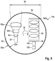
- FIG. 8 shows a second specific embodiment of the optical sensor according to the present invention.
- FIG. 9 shows one specific embodiment of the method according to the present invention.
- FIG. 1 shows a schematic illustration of a first specific embodiment of a device 110 a for detecting a soiling 51 a , 51 b and 51 c of a transparent cover 50 of at least one transmitting window and/or one receiving window of an optical sensor, in accordance with the present invention.
- Device 110 a includes a hologram structure 100 a in the process, which is designed as a holographic optical element (HOE), for example.
- Device 110 a additionally includes an image sensor 120 a and a processing unit 130 .
- device 110 a additionally includes a third illumination unit 70 a , which illuminates the transparent cover laterally from below in such a way that the light beams are reflected and deflected in the direction of hologram structure 100 a in the event of soiling 51 , 51 b and 51 c .
- a fourth illumination unit 70 b is provided, which illuminates the transparent cover laterally from above in such a way that the light beams are reflected and deflected in the direction of hologram structure 100 a in the event of soiling 51 , 51 b and 51 c .
- Hologram structure 100 a is used to deflect the reflected beams 71 a , 71 b , 72 a , 72 b , 73 a and 73 b in the direction of image sensor 120 a.
- image sensor 120 a is designed as an image sensor including a multitude of pixels 121 , 122 and 123 .
- Each pixel 121 , 122 and 123 is assigned a defined area 52 a , 52 b or 53 c of transparent cover 50 .
- pixel 121 is assigned area 52 a of transparent cover 50 .
- Hologram structure 100 a deflects the reflected light beams 71 a , 71 b , 72 a , 73 a and 73 b in such a way that the deflected light beams 71 c , 72 c , 73 c , 75 c , 76 c and 77 c incident on pixel 121 , 122 or 123 assigned to the respective area 52 a , 52 b or 53 c .
- hologram structure 100 a may, for example, be formed from multiple consecutively situated holograms.
- the individual holograms are each differently designed and deflect reflected light beams 71 a , 71 b , 72 a , 72 b , 73 a and 73 b in the direction of the respective pixel 121 , 122 or 123 as a function of the wavelength of light beams 71 a , 71 b , 72 a , 73 a and 73 b and/or the incidence angle of light beams 71 a , 71 b , 72 a , 72 b , 73 a and 73 b .
- multiple optical functions may be stored by holographic multiplexing in a layer of hologram structure 100 a , and light beams 71 c , 72 c , 73 c , 75 c , 76 c and 77 c may thus be deflected onto corresponding pixel 121 , 122 or 123 .
- hologram structure 100 a is designed as a volume hologram, which is designed to reflect the reflected light beams 71 a , 71 b , 72 a , 72 b , 73 a and 73 b in the direction of the image sensor.
- the volume hologram is transparent to light beams 78 which have a different wavelength and/or a different incidence angle compared to light beams 71 a , 71 b , 72 a , 72 b , 73 a and 73 b , and light beams 78 may pass through the volume hologram without deflection.
- Device 110 a additionally includes a processing unit 130 , which is designed to detect a soiling 51 a , 51 b or 51 c of transparent cover 50 as a function of the at least one detected image signal.
- processing unit 130 is designed to ascertain a mapping of a surface of transparent cover 50 .
- image sensor 120 which is designed as a CCD image sensor, for example, processing unit 130 receives image signals, from which a monochrome or even a color map of the surface of transparent cover 50 may be generated. For example, white dots on the generated mapping may indicate a soiling 51 , 51 b and 51 c.
- FIG. 2 schematically shows a representation of a second specific embodiment of a device 110 b for detecting a soiling 51 a , 51 b and 51 c of a transparent cover 50 of at least one transmitting window and/or one receiving window of an optical sensor, in accordance with the present invention.
- a first illumination unit 70 c is provided, which illuminates the inner side of transparent cover 50 in such a way that the light beams emitted by first illumination unit 70 a are reflected at inner side 55 b of transparent cover 50 in the event of soiling 51 a , 51 b and 51 c of transparent cover 50 .
- FIG. 3 schematically shows a first specific embodiment of a holographic cascade filter 140 , in accordance with the present invention.
- This holographic cascade filter 140 serves as a filter unit for light beams which do not have a defined wavelength range and/or entrance angle range.
- First hologram 100 a is designed as a transmission hologram and is used to deflect incident light which has the defined wavelength range and/or entrance angle range in the direction of a downstream second hologram 100 e .
- Incident light beams 116 a which are not situated within the defined wavelength range and/or entrance angle range may pass through first hologram 100 d linearly without deflection.
- Second hologram 100 e is designed as a reflection hologram and is also designed to reflect only incident light beams 116 b which have a defined wavelength range and/or a defined entrance angle range onto a downstream third reflection hologram 100 f . In this way, incrementally more and more light beams which do not correspond to a defined wavelength range and/or a defined entrance angle range are filtered out.
- holographic cascade filter 140 is designed in a curved shape and, after multiple reflections and corresponding filtering at one of reflection holograms 100 e , 100 f , 100 g and 100 g , a light beam 116 f falls on hologram 100 i designed as a transmission hologram.
- Transmission hologram 100 i is designed to diffract only light beams having a certain wavelength and/or a certain incidence angle and to deflect them onto pixel 125 a .
- the wavelength may correspond to the wavelength of the color red, for example, whereby the generation of a monochrome color map is made possible.
- FIG. 4 shows a holographic cascade filter 140 b , which has a straight shape and includes two waveguides 145 a and 145 b for two pixels 125 b and 125 c.
- a further reflection hologram 106 a is connected upstream from each of the two transmission holograms 106 b and 107 b , which filters undesirable signals, such as interfering signals, out of the optical path.
- the two subsequent transmission holograms 106 b and 107 b are designed to diffract light beams 127 b or 137 b having a wavelength range and/or an entrance angle range different from one another and to reflect them in the direction of the following reflection hologram 106 b or 107 c .
- FIG. 5 schematically shows an image sensor as it may be used by way of example in the above-described device.
- the image sensor includes a blue pixel 121 , a green pixel 123 and a red pixel 124 .
- Image sensor additionally includes an infrared pixel in the process.
- FIG. 6 schematically shows a generated mapping 90 which was generated from at least one detected image signal.
- Mapping 90 is represented as a monochrome color map 90 , and the white dots 91 on the mapping stem from light beams deflected with the aid of a hologram structure onto the image sensor.
- Such a pattern on the mapping arises, for example, in the case of rain drops and/or dust on an outer surface of the transparent cover.
- FIG. 7 in the side view, schematically shows a first specific embodiment of the optical sensor 10 a according to the present invention.
- Optical sensor 10 a is designed as a LIDAR sensor in this specific embodiment. It is represented by way of example how light beams 101 a , 102 a and 103 a , which are incident on transparent cover 50 at different incidence angles, thereupon strike a hologram structure 105 .
- Hologram structure 105 a is designed as a transmission hologram in this specific embodiment, and is situated on a curved outer side of a lens 110 of a receiving lens system 20 of the LIDAR sensor.
- Hologram structure 105 a deflects light beams 101 a , 102 a and 103 a in such a way that deflected light beams 101 b , 102 b and 103 b , in turn, are guided in receiving lens system 20 in such a way that the deflected light beams 101 b , 102 b and 103 b finally strike image sensor 120 .
- the image sensor of LIDAR sensor 10 a is used as image sensor 120 in the process.
- an interfering signal filter 46 is situated in front of image sensor 120 .
- Image sensor 120 is, in turn, designed to detect at least one image signal as a function of the deflected light beams.
- the downstream processing unit 130 in this specific embodiment, in turn, detects a possible soiling of transparent cover 50 as a function of the at least one detected image signal.
- FIG. 8 in the top view, shows a second specific embodiment of the optical sensor 10 b according to the present invention.
- optical sensor 10 b which is also designed as a LIDAR sensor, includes a housing 65 .
- a certain area of the circular housing 65 is designed as open toward the outside and thus forms transmitting and/or receiving window 64 of optical sensor 10 b .
- Transmitting and/or receiving window 64 is covered by a transparent cover 50 with respect to exterior surroundings of optical sensor 10 b .
- the circular housing 65 rotates together with transparent cover 50 .
- Laser 30 generates infrared radiation 40 , for example, which is directed with the aid of transmitting lens system 80 a , 80 b and 80 c and emitted to the outside into the surroundings.
- Light beams which are incident through transparent cover 50 are at least partially deflected with the aid of hologram structure 105 b onto image sensor 120 .
- FIG. 9 shows one specific embodiment of a method for detecting a soiling of a transparent cover of at least one transmitting window and/or one receiving window of an optical sensor.
- the method is carried out with the aid of a device according to the present invention.
- a first method step 200 light beams incident through a transparent cover, or light beams reflected at an inner side of the transparent cover, are at least partially deflected in the direction of an image sensor with the aid of at least one hologram structure.
- the deflected light beams are detected with the aid of the image sensor.
- a soiling of the transparent cover is identified with the aid of a processing unit, as a function of the at least one detected image signal.
- a mapping of a surface of the transparent cover is optionally generated as a function of the at least one detected image signal.
Landscapes
- Physics & Mathematics (AREA)
- Engineering & Computer Science (AREA)
- General Physics & Mathematics (AREA)
- Remote Sensing (AREA)
- Radar, Positioning & Navigation (AREA)
- Computer Networks & Wireless Communication (AREA)
- Health & Medical Sciences (AREA)
- Optics & Photonics (AREA)
- Signal Processing (AREA)
- Multimedia (AREA)
- General Health & Medical Sciences (AREA)
- Electromagnetism (AREA)
- Pathology (AREA)
- Immunology (AREA)
- Biochemistry (AREA)
- Analytical Chemistry (AREA)
- Chemical & Material Sciences (AREA)
- Life Sciences & Earth Sciences (AREA)
- Quality & Reliability (AREA)
- Computer Vision & Pattern Recognition (AREA)
- Theoretical Computer Science (AREA)
- Biomedical Technology (AREA)
- Diffracting Gratings Or Hologram Optical Elements (AREA)
- Holo Graphy (AREA)
Abstract
Description
Claims (17)
Applications Claiming Priority (3)
| Application Number | Priority Date | Filing Date | Title |
|---|---|---|---|
| DE102018209020.3A DE102018209020A1 (en) | 2018-06-07 | 2018-06-07 | Device, designed to detect contamination of at least one transmission window and / or a receiving window of a sensor |
| DE102018209020.3 | 2018-06-07 | ||
| PCT/EP2019/064267 WO2019233917A1 (en) | 2018-06-07 | 2019-06-03 | Device designed to detect soiling of at least one transmitting window and/or one receiving window of a sensor |
Publications (2)
| Publication Number | Publication Date |
|---|---|
| US20210067769A1 US20210067769A1 (en) | 2021-03-04 |
| US11368673B2 true US11368673B2 (en) | 2022-06-21 |
Family
ID=66810771
Family Applications (1)
| Application Number | Title | Priority Date | Filing Date |
|---|---|---|---|
| US17/043,104 Expired - Fee Related US11368673B2 (en) | 2018-06-07 | 2019-06-03 | Device designed for detecting a soiling of at least one transmitting window and/or one receiving window of a sensor |
Country Status (5)
| Country | Link |
|---|---|
| US (1) | US11368673B2 (en) |
| EP (1) | EP3803353A1 (en) |
| CN (1) | CN112262312A (en) |
| DE (1) | DE102018209020A1 (en) |
| WO (1) | WO2019233917A1 (en) |
Families Citing this family (7)
| Publication number | Priority date | Publication date | Assignee | Title |
|---|---|---|---|---|
| DE102019214841A1 (en) * | 2019-09-27 | 2021-04-01 | Robert Bosch Gmbh | Filter device for a lidar system |
| DE102021212020A1 (en) | 2021-10-26 | 2023-04-27 | Robert Bosch Gesellschaft mit beschränkter Haftung | Method for detecting soiling on a lens unit of a camera of an agricultural working machine |
| DE102022000235B4 (en) | 2022-01-24 | 2024-05-29 | Mercedes-Benz Group AG | Method for cleaning a viewing window of a lidar |
| DE102022104939A1 (en) | 2022-03-02 | 2023-09-07 | Audi Aktiengesellschaft | Driverless transport vehicle |
| US12202336B2 (en) | 2022-03-22 | 2025-01-21 | GM Global Technology Operations LLC | Head-up display system having a holographic panel comprising a first layer and a second layer |
| US11835720B2 (en) * | 2022-03-22 | 2023-12-05 | GM Global Technology Operations LLC | Head-up display system having a holographic panel |
| US12345897B2 (en) | 2022-03-22 | 2025-07-01 | GM Global Technology Operations LLC | Glare mitigation module for a head-up display system |
Citations (14)
| Publication number | Priority date | Publication date | Assignee | Title |
|---|---|---|---|---|
| DE19512864C1 (en) | 1995-04-06 | 1996-08-22 | Sekurit Saint Gobain Deutsch | Car glass for a rain sensor |
| DE19530289A1 (en) | 1995-08-17 | 1997-02-20 | Bosch Gmbh Robert | Sensor for determining visibility and rain cover |
| DE19701258A1 (en) | 1996-01-18 | 1997-07-24 | Itt Mfg Enterprises Inc | Rain sensing system for transparent material surfaces e.g. windscreens |
| EP0999104A2 (en) | 1998-11-02 | 2000-05-10 | Central Glass Company, Limited | Water droplet sensor and exposure system for hologram |
| DE10049401A1 (en) | 2000-10-05 | 2002-04-25 | Hsm Gmbh | humidity sensor |
| DE10229239A1 (en) | 2002-06-28 | 2004-01-15 | Robert Bosch Gmbh | Rain sensor, especially for a motor vehicle |
| DE10314704A1 (en) | 2003-03-31 | 2004-10-14 | Robert Bosch Gmbh | Rain sensor for a motor vehicle has a measured section made up of a transmitter for emitting rays and a receiver for detecting rays |
| DE102005062785A1 (en) | 2005-12-28 | 2007-07-05 | Robert Bosch Gmbh | Rain sensor for motor vehicle, has optical waveguide with coupling units, which are formed by layer-shaped pieces made of photopolymer, in which volume holograms are incorporated, where pieces are arranged between waveguide core and casing |
| DE102010028347A1 (en) | 2010-04-29 | 2011-11-03 | Robert Bosch Gmbh | Sensor arrangement on a motor vehicle |
| WO2014005585A1 (en) | 2012-07-05 | 2014-01-09 | Continental Automotive Gmbh | Camera system for detecting the state of a vehicle window |
| DE102013210887A1 (en) | 2013-06-11 | 2014-12-11 | Robert Bosch Gmbh | Optical sensor arrangement for a vehicle and vehicle with such a sensor arrangement |
| US20150293498A1 (en) * | 2012-10-30 | 2015-10-15 | Centre National De La Recherche Scientifique | Self-reference holographic imaging system |
| US20160041525A1 (en) * | 2014-08-08 | 2016-02-11 | Hitachi-Lg Data Storage, Inc. | Holographic memory device |
| WO2019141644A1 (en) | 2018-01-16 | 2019-07-25 | Robert Bosch Gmbh | Detection device for detecting contamination |
Family Cites Families (8)
| Publication number | Priority date | Publication date | Assignee | Title |
|---|---|---|---|---|
| JPH09105724A (en) * | 1995-08-04 | 1997-04-22 | Kobe Steel Ltd | Surface inspection equipment |
| KR100403599B1 (en) * | 2001-11-06 | 2003-10-30 | 삼성전자주식회사 | Illumination system and a projection system imploying it |
| DE102006044786A1 (en) * | 2006-09-14 | 2008-03-27 | Schefenacker Vision Systems Germany Gmbh | Camera system, method for operating a camera system and sensor device of a camera system |
| DE102013211735A1 (en) * | 2013-06-21 | 2014-12-24 | Continental Automotive Gmbh | Device for detecting moisture |
| JP5946970B2 (en) * | 2013-09-27 | 2016-07-06 | 富士フイルム株式会社 | Imaging apparatus and imaging method |
| DE102014211071A1 (en) * | 2014-06-11 | 2015-12-17 | Robert Bosch Gmbh | Vehicle lidar system |
| DE102015007794A1 (en) * | 2015-06-19 | 2015-12-10 | Daimler Ag | Method and device for detecting moisture and / or contamination on an outside of a cover of an image sensor |
| CN205607811U (en) * | 2016-04-01 | 2016-09-28 | 黄恺 | Device based on laser holography formation of image method analysis grain shape |
-
2018
- 2018-06-07 DE DE102018209020.3A patent/DE102018209020A1/en not_active Withdrawn
-
2019
- 2019-06-03 EP EP19729474.7A patent/EP3803353A1/en not_active Withdrawn
- 2019-06-03 CN CN201980038457.2A patent/CN112262312A/en active Pending
- 2019-06-03 WO PCT/EP2019/064267 patent/WO2019233917A1/en not_active Ceased
- 2019-06-03 US US17/043,104 patent/US11368673B2/en not_active Expired - Fee Related
Patent Citations (17)
| Publication number | Priority date | Publication date | Assignee | Title |
|---|---|---|---|---|
| DE19512864C1 (en) | 1995-04-06 | 1996-08-22 | Sekurit Saint Gobain Deutsch | Car glass for a rain sensor |
| EP0736426A1 (en) | 1995-04-06 | 1996-10-09 | Saint-Gobain Vitrage | Automobile glazing for a rain sensor |
| DE19530289A1 (en) | 1995-08-17 | 1997-02-20 | Bosch Gmbh Robert | Sensor for determining visibility and rain cover |
| DE19701258A1 (en) | 1996-01-18 | 1997-07-24 | Itt Mfg Enterprises Inc | Rain sensing system for transparent material surfaces e.g. windscreens |
| EP0999104A2 (en) | 1998-11-02 | 2000-05-10 | Central Glass Company, Limited | Water droplet sensor and exposure system for hologram |
| US6307198B1 (en) * | 1998-11-02 | 2001-10-23 | Central Glass Company, Limited | Water droplet sensor and exposure system for hologram |
| DE10049401A1 (en) | 2000-10-05 | 2002-04-25 | Hsm Gmbh | humidity sensor |
| DE10229239A1 (en) | 2002-06-28 | 2004-01-15 | Robert Bosch Gmbh | Rain sensor, especially for a motor vehicle |
| DE10314704A1 (en) | 2003-03-31 | 2004-10-14 | Robert Bosch Gmbh | Rain sensor for a motor vehicle has a measured section made up of a transmitter for emitting rays and a receiver for detecting rays |
| DE102005062785A1 (en) | 2005-12-28 | 2007-07-05 | Robert Bosch Gmbh | Rain sensor for motor vehicle, has optical waveguide with coupling units, which are formed by layer-shaped pieces made of photopolymer, in which volume holograms are incorporated, where pieces are arranged between waveguide core and casing |
| US20080212151A1 (en) | 2005-12-28 | 2008-09-04 | Frank Wolf | Rain Sensor, for a Motor Vehicle in Particular, and Method for Producing the Rain Sensor |
| DE102010028347A1 (en) | 2010-04-29 | 2011-11-03 | Robert Bosch Gmbh | Sensor arrangement on a motor vehicle |
| WO2014005585A1 (en) | 2012-07-05 | 2014-01-09 | Continental Automotive Gmbh | Camera system for detecting the state of a vehicle window |
| US20150293498A1 (en) * | 2012-10-30 | 2015-10-15 | Centre National De La Recherche Scientifique | Self-reference holographic imaging system |
| DE102013210887A1 (en) | 2013-06-11 | 2014-12-11 | Robert Bosch Gmbh | Optical sensor arrangement for a vehicle and vehicle with such a sensor arrangement |
| US20160041525A1 (en) * | 2014-08-08 | 2016-02-11 | Hitachi-Lg Data Storage, Inc. | Holographic memory device |
| WO2019141644A1 (en) | 2018-01-16 | 2019-07-25 | Robert Bosch Gmbh | Detection device for detecting contamination |
Non-Patent Citations (1)
| Title |
|---|
| International Search Report for PCT/EP2019/064267, dated Sep. 25, 2019. |
Also Published As
| Publication number | Publication date |
|---|---|
| EP3803353A1 (en) | 2021-04-14 |
| US20210067769A1 (en) | 2021-03-04 |
| DE102018209020A1 (en) | 2019-12-12 |
| CN112262312A (en) | 2021-01-22 |
| WO2019233917A1 (en) | 2019-12-12 |
Similar Documents
| Publication | Publication Date | Title |
|---|---|---|
| US20210067769A1 (en) | Device designed for detecting a soiling of at least one transmitting window and/or one receiving window of a sensor | |
| US9335264B2 (en) | Detection of raindrops on a pane by means of a camera and lighting | |
| US8670024B2 (en) | Camera objective and camera system | |
| US7855353B2 (en) | Vehicle window camera arrangement having camera with camera portions handling separate image and intensity acquisition functions using same light-guiding element portion | |
| US10914839B2 (en) | Optical assembly and a lidar device having an optical assembly of this type | |
| US20070034783A1 (en) | Multitasking radiation sensor | |
| US20090116030A1 (en) | Fingerprint sensor using a spectral filter and a holographic optical element | |
| US11946873B2 (en) | Detection device for detecting contamination | |
| CN114009001A (en) | Camera arrangement for generating images of the surroundings | |
| JP2019502921A (en) | LIDAR scanning apparatus and LIDAR scanning system | |
| KR20180111813A (en) | An imaging device with improved autofocus performance | |
| KR20210120002A (en) | Screen comprising a transparent base body | |
| JP3682834B2 (en) | Optical device using wavelength tunable interference filter | |
| CN110794378B (en) | LiDAR devices for object detection | |
| CN110850388B (en) | Lidar device having at least one scattering disk element | |
| DE102018209015A1 (en) | Device and method for detecting contamination of at least one transmission window and / or a receiving window of a sensor | |
| US11501098B2 (en) | Information code reader | |
| US11592525B2 (en) | Filter device for an optical sensor | |
| EP4341132B1 (en) | Rain sensor system, vehicle and method for detecting rain | |
| JP2015194388A (en) | Imaging apparatus and imaging system | |
| CN101071261B (en) | Detection method of coating surface of infrared cut-off filter | |
| JP4650469B2 (en) | Imaging apparatus and lens abnormality diagnosis system | |
| CN114120850A (en) | Display device | |
| JP5136758B2 (en) | Composite optical system and optical apparatus having this composite optical system | |
| JPH0493915A (en) | Spectral image formation optical system |
Legal Events
| Date | Code | Title | Description |
|---|---|---|---|
| FEPP | Fee payment procedure |
Free format text: ENTITY STATUS SET TO UNDISCOUNTED (ORIGINAL EVENT CODE: BIG.); ENTITY STATUS OF PATENT OWNER: LARGE ENTITY |
|
| STPP | Information on status: patent application and granting procedure in general |
Free format text: DOCKETED NEW CASE - READY FOR EXAMINATION |
|
| STPP | Information on status: patent application and granting procedure in general |
Free format text: NON FINAL ACTION MAILED |
|
| STPP | Information on status: patent application and granting procedure in general |
Free format text: RESPONSE TO NON-FINAL OFFICE ACTION ENTERED AND FORWARDED TO EXAMINER |
|
| STPP | Information on status: patent application and granting procedure in general |
Free format text: NOTICE OF ALLOWANCE MAILED -- APPLICATION RECEIVED IN OFFICE OF PUBLICATIONS |
|
| AS | Assignment |
Owner name: ROBERT BOSCH GMBH, GERMANY Free format text: ASSIGNMENT OF ASSIGNORS INTEREST;ASSIGNORS:FREDERIKSEN, ANNETTE;HARTMANN, STEFANIE;SIGNING DATES FROM 20210719 TO 20220320;REEL/FRAME:059385/0520 |
|
| STPP | Information on status: patent application and granting procedure in general |
Free format text: PUBLICATIONS -- ISSUE FEE PAYMENT VERIFIED |
|
| STCF | Information on status: patent grant |
Free format text: PATENTED CASE |
|
| FEPP | Fee payment procedure |
Free format text: MAINTENANCE FEE REMINDER MAILED (ORIGINAL EVENT CODE: REM.); ENTITY STATUS OF PATENT OWNER: LARGE ENTITY |
|
| LAPS | Lapse for failure to pay maintenance fees |
Free format text: PATENT EXPIRED FOR FAILURE TO PAY MAINTENANCE FEES (ORIGINAL EVENT CODE: EXP.); ENTITY STATUS OF PATENT OWNER: LARGE ENTITY |
|
| STCH | Information on status: patent discontinuation |
Free format text: PATENT EXPIRED DUE TO NONPAYMENT OF MAINTENANCE FEES UNDER 37 CFR 1.362 |