US11368302B2 - Key management device and processor chip having bypass channels - Google Patents
Key management device and processor chip having bypass channels Download PDFInfo
- Publication number
- US11368302B2 US11368302B2 US17/014,767 US202017014767A US11368302B2 US 11368302 B2 US11368302 B2 US 11368302B2 US 202017014767 A US202017014767 A US 202017014767A US 11368302 B2 US11368302 B2 US 11368302B2
- Authority
- US
- United States
- Prior art keywords
- key
- management device
- encryption
- decryption
- key management
- Prior art date
- Legal status (The legal status is an assumption and is not a legal conclusion. Google has not performed a legal analysis and makes no representation as to the accuracy of the status listed.)
- Active, expires
Links
Images


Classifications
-
- H—ELECTRICITY
- H04—ELECTRIC COMMUNICATION TECHNIQUE
- H04L—TRANSMISSION OF DIGITAL INFORMATION, e.g. TELEGRAPHIC COMMUNICATION
- H04L9/00—Cryptographic mechanisms or cryptographic arrangements for secret or secure communications; Network security protocols
- H04L9/32—Cryptographic mechanisms or cryptographic arrangements for secret or secure communications; Network security protocols including means for verifying the identity or authority of a user of the system or for message authentication, e.g. authorization, entity authentication, data integrity or data verification, non-repudiation, key authentication or verification of credentials
- H04L9/3236—Cryptographic mechanisms or cryptographic arrangements for secret or secure communications; Network security protocols including means for verifying the identity or authority of a user of the system or for message authentication, e.g. authorization, entity authentication, data integrity or data verification, non-repudiation, key authentication or verification of credentials using cryptographic hash functions
- H04L9/3242—Cryptographic mechanisms or cryptographic arrangements for secret or secure communications; Network security protocols including means for verifying the identity or authority of a user of the system or for message authentication, e.g. authorization, entity authentication, data integrity or data verification, non-repudiation, key authentication or verification of credentials using cryptographic hash functions involving keyed hash functions, e.g. message authentication codes [MACs], CBC-MAC or HMAC
-
- G—PHYSICS
- G06—COMPUTING OR CALCULATING; COUNTING
- G06F—ELECTRIC DIGITAL DATA PROCESSING
- G06F13/00—Interconnection of, or transfer of information or other signals between, memories, input/output devices or central processing units
- G06F13/14—Handling requests for interconnection or transfer
- G06F13/36—Handling requests for interconnection or transfer for access to common bus or bus system
- G06F13/362—Handling requests for interconnection or transfer for access to common bus or bus system with centralised access control
-
- G—PHYSICS
- G06—COMPUTING OR CALCULATING; COUNTING
- G06F—ELECTRIC DIGITAL DATA PROCESSING
- G06F21/00—Security arrangements for protecting computers, components thereof, programs or data against unauthorised activity
- G06F21/70—Protecting specific internal or peripheral components, in which the protection of a component leads to protection of the entire computer
- G06F21/71—Protecting specific internal or peripheral components, in which the protection of a component leads to protection of the entire computer to assure secure computing or processing of information
- G06F21/72—Protecting specific internal or peripheral components, in which the protection of a component leads to protection of the entire computer to assure secure computing or processing of information in cryptographic circuits
-
- G—PHYSICS
- G11—INFORMATION STORAGE
- G11C—STATIC STORES
- G11C11/00—Digital stores characterised by the use of particular electric or magnetic storage elements; Storage elements therefor
- G11C11/21—Digital stores characterised by the use of particular electric or magnetic storage elements; Storage elements therefor using electric elements
- G11C11/34—Digital stores characterised by the use of particular electric or magnetic storage elements; Storage elements therefor using electric elements using semiconductor devices
- G11C11/40—Digital stores characterised by the use of particular electric or magnetic storage elements; Storage elements therefor using electric elements using semiconductor devices using transistors
- G11C11/41—Digital stores characterised by the use of particular electric or magnetic storage elements; Storage elements therefor using electric elements using semiconductor devices using transistors forming static cells with positive feedback, i.e. cells not needing refreshing or charge regeneration, e.g. bistable multivibrator or Schmitt trigger
- G11C11/412—Digital stores characterised by the use of particular electric or magnetic storage elements; Storage elements therefor using electric elements using semiconductor devices using transistors forming static cells with positive feedback, i.e. cells not needing refreshing or charge regeneration, e.g. bistable multivibrator or Schmitt trigger using field-effect transistors only
-
- G—PHYSICS
- G11—INFORMATION STORAGE
- G11C—STATIC STORES
- G11C17/00—Read-only memories programmable only once; Semi-permanent stores, e.g. manually-replaceable information cards
- G11C17/14—Read-only memories programmable only once; Semi-permanent stores, e.g. manually-replaceable information cards in which contents are determined by selectively establishing, breaking or modifying connecting links by permanently altering the state of coupling elements, e.g. PROM
- G11C17/18—Auxiliary circuits, e.g. for writing into memory
-
- H—ELECTRICITY
- H04—ELECTRIC COMMUNICATION TECHNIQUE
- H04L—TRANSMISSION OF DIGITAL INFORMATION, e.g. TELEGRAPHIC COMMUNICATION
- H04L9/00—Cryptographic mechanisms or cryptographic arrangements for secret or secure communications; Network security protocols
- H04L9/06—Cryptographic mechanisms or cryptographic arrangements for secret or secure communications; Network security protocols the encryption apparatus using shift registers or memories for block-wise or stream coding, e.g. DES systems or RC4; Hash functions; Pseudorandom sequence generators
- H04L9/0618—Block ciphers, i.e. encrypting groups of characters of a plain text message using fixed encryption transformation
- H04L9/0631—Substitution permutation network [SPN], i.e. cipher composed of a number of stages or rounds each involving linear and nonlinear transformations, e.g. AES algorithms
-
- H—ELECTRICITY
- H04—ELECTRIC COMMUNICATION TECHNIQUE
- H04L—TRANSMISSION OF DIGITAL INFORMATION, e.g. TELEGRAPHIC COMMUNICATION
- H04L9/00—Cryptographic mechanisms or cryptographic arrangements for secret or secure communications; Network security protocols
- H04L9/06—Cryptographic mechanisms or cryptographic arrangements for secret or secure communications; Network security protocols the encryption apparatus using shift registers or memories for block-wise or stream coding, e.g. DES systems or RC4; Hash functions; Pseudorandom sequence generators
- H04L9/0643—Hash functions, e.g. MD5, SHA, HMAC or f9 MAC
-
- H—ELECTRICITY
- H04—ELECTRIC COMMUNICATION TECHNIQUE
- H04L—TRANSMISSION OF DIGITAL INFORMATION, e.g. TELEGRAPHIC COMMUNICATION
- H04L9/00—Cryptographic mechanisms or cryptographic arrangements for secret or secure communications; Network security protocols
- H04L9/08—Key distribution or management, e.g. generation, sharing or updating, of cryptographic keys or passwords
- H04L9/0894—Escrow, recovery or storing of secret information, e.g. secret key escrow or cryptographic key storage
- H04L9/0897—Escrow, recovery or storing of secret information, e.g. secret key escrow or cryptographic key storage involving additional devices, e.g. trusted platform module [TPM], smartcard or USB
-
- H—ELECTRICITY
- H04—ELECTRIC COMMUNICATION TECHNIQUE
- H04L—TRANSMISSION OF DIGITAL INFORMATION, e.g. TELEGRAPHIC COMMUNICATION
- H04L9/00—Cryptographic mechanisms or cryptographic arrangements for secret or secure communications; Network security protocols
- H04L9/30—Public key, i.e. encryption algorithm being computationally infeasible to invert or user's encryption keys not requiring secrecy
- H04L9/3006—Public key, i.e. encryption algorithm being computationally infeasible to invert or user's encryption keys not requiring secrecy underlying computational problems or public-key parameters
- H04L9/302—Public key, i.e. encryption algorithm being computationally infeasible to invert or user's encryption keys not requiring secrecy underlying computational problems or public-key parameters involving the integer factorization problem, e.g. RSA or quadratic sieve [QS] schemes
-
- H—ELECTRICITY
- H04—ELECTRIC COMMUNICATION TECHNIQUE
- H04L—TRANSMISSION OF DIGITAL INFORMATION, e.g. TELEGRAPHIC COMMUNICATION
- H04L9/00—Cryptographic mechanisms or cryptographic arrangements for secret or secure communications; Network security protocols
- H04L9/30—Public key, i.e. encryption algorithm being computationally infeasible to invert or user's encryption keys not requiring secrecy
- H04L9/3066—Public key, i.e. encryption algorithm being computationally infeasible to invert or user's encryption keys not requiring secrecy involving algebraic varieties, e.g. elliptic or hyper-elliptic curves
-
- H—ELECTRICITY
- H04—ELECTRIC COMMUNICATION TECHNIQUE
- H04L—TRANSMISSION OF DIGITAL INFORMATION, e.g. TELEGRAPHIC COMMUNICATION
- H04L2209/00—Additional information or applications relating to cryptographic mechanisms or cryptographic arrangements for secret or secure communication H04L9/00
- H04L2209/12—Details relating to cryptographic hardware or logic circuitry
-
- Y—GENERAL TAGGING OF NEW TECHNOLOGICAL DEVELOPMENTS; GENERAL TAGGING OF CROSS-SECTIONAL TECHNOLOGIES SPANNING OVER SEVERAL SECTIONS OF THE IPC; TECHNICAL SUBJECTS COVERED BY FORMER USPC CROSS-REFERENCE ART COLLECTIONS [XRACs] AND DIGESTS
- Y04—INFORMATION OR COMMUNICATION TECHNOLOGIES HAVING AN IMPACT ON OTHER TECHNOLOGY AREAS
- Y04S—SYSTEMS INTEGRATING TECHNOLOGIES RELATED TO POWER NETWORK OPERATION, COMMUNICATION OR INFORMATION TECHNOLOGIES FOR IMPROVING THE ELECTRICAL POWER GENERATION, TRANSMISSION, DISTRIBUTION, MANAGEMENT OR USAGE, i.e. SMART GRIDS
- Y04S40/00—Systems for electrical power generation, transmission, distribution or end-user application management characterised by the use of communication or information technologies, or communication or information technology specific aspects supporting them
- Y04S40/20—Information technology specific aspects, e.g. CAD, simulation, modelling, system security
Definitions
- the present invention relates to a technical field of data transmission, and more particularly to a key management device and a processor chip having bypass channels.
- a conventional key management device and a conventional cryptographic device have to be connected to a bus. If the bus is tapped, the key taken out by the key management device may be obtained by the eavesdropper, so there is a risk of the key being stolen.
- An objective of the present invention is to provide a key management device and a processor chip having bypass channels to solve the conventional technical problems.
- the key management device includes: a static random-access memory (SRAM); a register; and an arbitration circuit, electrically connected to an encryption/decryption device having a plurality of encryption/decryption circuits, and there is a bypass channel between each encryption/decryption circuit and the arbitration circuit; and a control circuit configured to set a key lookup table in the static random-access memory or the register, and manage a key database.
- the key database comprises the static random-access memory and a one-time programmable (OTP) memory disposed outside the key management device, and the key database is configured to store at least one key.
- OTP one-time programmable
- the key lookup table comprises a key number and metadata of each of the at least one key stored in the key database.
- the control circuit In response to the control circuit retrieving a specific key corresponding to a specific key number indicated by a key read command, the control circuit directly transmits the specific key to the corresponding encryption/decryption circuit through the bypass channel.
- the key database comprises a flash memory disposed outside the key management device.
- the key management device and the encryption/decryption device are independent hardware circuits, and the key management device and the encryption/decryption device are electrically connected to the bus.
- the arbitration circuit is configured to select one of a signal from the bus or another signal from one of the encryption/decryption circuits to communicate with the control circuit.
- attributes of the metadata of the key in the key lookup table comprise a key size, an owner, a security level, a privilege level, a readable attribute, a revoke attribute, a booting state, and a storage location.
- the plurality of encryption/decryption circuits comprise an advanced encryption standard (AES) encryption/decryption circuit, a keyed-hash message authentication code (HMAC) encryption/decryption circuit, and an elliptic curve cryptography (ECC) encryption/decryption circuit, and an RSA encryption/decryption circuit, a random number generating circuit, or a combination thereof.
- AES advanced encryption standard
- HMAC keyed-hash message authentication code
- ECC elliptic curve cryptography
- the processor chip includes: a processor; a one-time programmable (OTP) memory; a flash memory; an encryption/decryption device, comprising a plurality of encryption/decryption circuits; and a key management device, electrically connected to the processor, the OTP memory, the flash memory, and the encryption/decryption device through a bus.
- the key management device comprises: a static random-access memory (SRAM); a register; and an arbitration circuit, wherein there is a bypass channel between each encryption/decryption circuit and the arbitration circuit; and a control circuit configured to set a key lookup table in the static random-access memory or the register, and manage a key database.
- the key database comprises the static random-access memory and a one-time programmable (OTP) memory disposed outside the key management device, and the key database is configured to store at least one key.
- the key lookup table comprises a key number and metadata of each of the at least one key stored in the key database; wherein in response to the control circuit retrieving a specific key corresponding to a specific key number indicated by a key read command, the control circuit directly transmit the specific key to the corresponding encryption/decryption circuit through the bypass channel.
- FIG. 1 is a block diagram of a control system of an embodiment of the present invention.
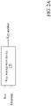
- FIGS. 2A and 2B are schematic views of operations of creating a key, according to one embodiment of the present invention.
- FIGS. 2C and 2D are schematic views of operations of reading a key, according to one embodiment of the present invention.
- FIGS. 2E and 2F are schematic views of operations of deleting a key, according to one embodiment of the present invention.
- FIG. 3 is a flowchart of an operation of creating a new key by a key management device, according to one embodiment of the present invention.
- FIG. 1 is a block diagram of a control system of an embodiment of the present invention.
- a control system 10 comprises a processor chip 110 and a memory unit 130 , a storage device 140 , a transmission interface 150 , and at least one peripheral device 160 .
- the processor chip 110 is electrically connected to the memory unit 130 via the bus 21 .
- the bus 21 can be an advance high-efficiency bus (AHB).
- the transmission interface 150 and the peripheral device 160 can be electrically connected to the bus 22 , and the buses 21 and 22 can communicate with each other via the bridge 23 .
- the bus 22 can be an advanced system bus (ASB) or an advance peripheral bus (APB); however, the present invention is not limited to the examples described herein.
- the processor chip 110 can comprise a central processing unit (CPU) 111 (or a microprocessor), a volatile memory 112 , a flash memory 113 , and a one-time programmable (OTP) memory 114 , a graphic processing unit (GPU) 120 , a key management device 170 and an encryption/decryption device 180 .
- the volatile memory 112 can be a static random access memory (SRAM).
- the flash memory 113 can be a NAND flash memory.
- the OTP memory 114 can be referred as a programmable read-only memory (PROM), which can use a nonvolatile memory having a lock-bit register, for example, the nonvolatile memory can be implemented by a flash memory, an erasable programmable read-only (EPROM) memory or an electrically erasable programmable read-only (EEPROM) memory.
- PROM programmable read-only memory
- EPROM erasable programmable read-only
- EEPROM electrically erasable programmable read-only
- the central processing unit 111 can modify the lock-bit register of the OTP memory 114 , for example, the central processing unit 111 can modify the lock bit from 1, which indicates a non-locked state, to 0, which indicates a locked state, so as to indicate that the data stored in the OTP memory 114 is unable to be modified again, and the lock bit is unable to be modified from 0 to 1.
- the graphic processing unit 120 can be an individual graphic processor, or integrated into the central processing unit 111 .
- the memory unit 130 can be a volatile memory, such as dynamic random access memory (DRAM); however, the present invention is not limited to the examples described herein.
- the storage device 140 can be a nonvolatile memory, such as a hard disk drive, a solid-state drive (SSD), a flash memory, or an ROM memory; however, the present invention is not limited to the examples described herein. In some embodiments, the storage device 140 can be electrically connected to the bus 22 .
- the storage device 140 can store at least one application 141 and an operating system 142 such as Windows, Linux, MacOS or an embedded OS.
- the processor chip 110 can read and store the operating system 142 and the application 141 to the memory unit 130 for execution.
- the transmission interface 150 comprises at least one data transmission interface, such as a USB interface, a USB Type-C interface, a Thunderbolt interface, a general-purpose input/output (GPIO) interface, a universal asynchronous receiver/transmitter (UART) interface, a serial peripheral interface (SPI) interface, an inter-integrated circuit (I2C) interface, or a combination thereof; however, the present invention is not limited to the examples described herein.
- the peripheral device 160 can include an input device, such as a keyboard, a mouse, and a touch pad, and so on; however, the present invention is not limited to the examples described herein.
- the key management device 170 can be a hardware circuit of an intelligent key storage device, and this hardware circuit can be implemented by an application-specific integrated circuit (ASIC) or a field programmable gate array (FPGA).
- ASIC application-specific integrated circuit
- FPGA field programmable gate array
- the key management device 170 can operate different key according to a control command of the processor chip 110 , for example, the key management device 170 can perform operations of adding a key, reading a key, erasing or revoking one of keys, erasing or revoking all keys; however, the present invention is not limited to the examples described herein.
- the key management device 170 comprises a control circuit 171 and a bus wrapper 172 , an arbitration (ARB) circuit 173 , a register 174 and a static random-access memory (SRAM) 175 .
- the control circuit 171 can control various operations of key, such as the operations of creating key, reading key, deleting single key, and deleting all keys.
- the bus wrapper 172 can provide a conversion interface between signals of an internal device of the key management device 170 and signals of the bus 21 .
- the arbitration circuit 173 can be used to select the signal from bus 21 (e.g., a signal or command sent from the CPU 111 ) or the bypass signal from the encryption/decryption device 180 (e.g., through bypass channels 1801 to 1805 ).
- the register 174 can be used to record a key number of each key and fields of metadata corresponding to each key. The key information recorded in the register 174 can be called as a key lookup table.
- the control circuit 171 can store the key lookup table in the static random-access memory (SRAM) 175 .
- the static random-access memory (SRAM) 175 can be used as a storage space of a key database, to store at least one key.
- control circuit 171 can back up the key lookup table to the static random-access memory (SRAM) 175 or the flash memory such as the flash memory 113 of the processor chip 110 or the flash memory of the storage device 140 .
- SRAM static random-access memory
- flash memory such as the flash memory 113 of the processor chip 110 or the flash memory of the storage device 140 .
- the encryption/decryption (cryptographic) device 180 can be a hardware circuit supporting various encryption/decryption algorithms, and the encryption/decryption device 180 includes hardware circuits corresponding to various encryption/decryption algorithms, such as an advanced encryption standard (AES) encryption/decryption circuit 181 , a keyed-hash message authentication code (HMAC) encryption/decryption circuit 182 , an elliptic curve cryptography (ECC) encryption/decryption circuit 183 , an RSA encryption/decryption circuit 184 , a random number generating (RNG) circuit 185 , or a combination thereof, and these hardware circuits can perform hardware acceleration for corresponding encryption/decryption algorithms.
- AES advanced encryption standard
- HMAC keyed-hash message authentication code
- ECC elliptic curve cryptography
- RNG random number generating
- the encryption/decryption circuits 181 - 184 are abbreviated as E/D circuits 181 - 184 , as shown in FIG. 1 .
- the random number generating circuit 185 can be a pseudorandom number generating circuit or a true random number generating circuit.
- Each of encryption/decryption circuits 181 to 185 has a respective bypass channel (e.g., bypass channels 1801 to 1805 ) to directly communicate with the key management device 170 using bypass signals without passing through bus 21 .
- the encryption/decryption device 180 further includes an arbitration (ARB) circuit 187 that is configured to determine whether to allow the encryption/decryption circuits 181 to 185 to use the command and data from bus 21 according to a predetermined arbitration mechanism. For example, the command issued from the CPU 111 needs to pass through bus 21 and the arbitration circuit 187 to be transmitted to the encryption/decryption circuits 181 to 185 , and the encrypted or decrypted content of the encryption/decryption circuits 181 to 185 still needs to pass through bus 21 and arbitration circuit 187 to be transmitted to the CPU 111 .
- ARB arbitration
- the key management device 170 and the encryption/decryption device 180 are independent hardware circuits, for example, can be regarded as independent semiconductor intellectual properties, and the key management device 170 and the encryption/decryption device 180 generally communicate with each other through bus 21 . Because the special mechanism of key management requires high security, and the key management device 170 and the encryption/decryption device 180 can communicate through the bypass channels 1801 to 1805 . For example, after the key management device 170 has retrieved the key, the retrieved key can be directly transmitted to the corresponding encryption/decryption circuit through the corresponding bypass channel for decryption without passing through bus 21 . Accordingly, the security of the control system 10 can be further improved to avoid the risk of the bus 21 being tapped to expose the key.
- the different applications 141 can use different encryption/decryption algorithms to encrypt the to-be-encrypted contents (such as user password), respectively; for example, the encryption/decryption circuits 181 ⁇ 185 disposed in the encryption/decryption device 180 are used to perform encryption/decryption operations. Different encryption/decryption algorithms may use different key sizes, such as in a range of 64 bits to 4096 bits. After the encryption/decryption device 180 completely encrypts the to-be-encrypted content, the encryption/decryption device 180 can transmit the key to the key management device 170 for key management.
- the key management device 170 can have different operations for key management, such as operation of storing or adding key, reading key, erasing or deleting single key, erasing or deleting all keys.
- the key management device 170 can receive a key and metadata corresponding to the key, from the processor chip 110 (or the encryption/decryption device 180 ).
- attribute fields of the metadata can include key size, owner, security level, privilege level, readable attribute, revoke attribute and the booting state, and so on; however, the present invention is not limited to the examples described herein.
- the content of each field of the metadata will be described in the following paragraphs.
- the key size for example, can be expressed by an amount of bits of a key, such as 80 bits, 128 bits, or 256 bits.
- the encryption/decryption device 180 can support a key size in a range of 64 bits to 4096 bits.
- the owner attribute for example, can indicate an owner of a key, and the user not owning the key is unable to read the key.
- a key owner can be set according to different requirements, for example, a key owner can be set as CPU, the processor chip 110 , AES, HMAC, ECC and RSA. For example, when a field of a key owner in metadata of a key is set as AES, it indicates that the AES encryption/decryption circuit of the encryption/decryption device 180 can read this key.
- the security-level attribute indicates a security level of a key, and, for example, can be classified into a secure level and a non-secure level.
- the key with the secure level can be used by the owner with the same secure level, and it is not necessary to check the security level of the owner for the key with the non-secure level.
- the security-level attribute in the metadata of the key must be in cooperation with the processor chip 110 to be effective.
- the processor chip 110 can be classified into a secure processor or a non-secure processor, and the field setting of the security level of the metadata of the key can be effective when the processor chip 110 is a secure processor.
- the processor chip 110 is a non-secure processor, the field setting of the security level of the metadata of the key is not effective.
- the privilege-level attribute indicates a level of privilege of the key, and for example, can be classified into a privilege level and a non-privilege level.
- the key with privilege level can be used by the owner with the same privilege level, and the key with the non-privilege level does not need to check the level of the privilege of the owner.
- Different user may have different permissions, for example, an administrator or a super user has the highest privilege level, and can access the key set with the privilege level; a general user not with the privilege level is unable to access the key with the privilege level.
- the readable attribute indicates whether the key can be read by the processor chip 110 .
- the owner field of the key is CPU, it indicates that the key can be readable for the processor chip 110 .
- the key management device 170 can determine, according to the readable attribute of the key, whether the processor chip 110 can read the key.
- the revoke attribute is recorded in an internal register of the key management device 170 , and unable to be set when the key is created.
- the key management device 170 can set the revoke attribute of the key as 0 , and it indicates that this key can be used normally.
- the key management device 170 possibly deletes the key stored in the flash memory or the OTP memory; however, the key stored in the flash memory or the OTP memory may be unable to be actually deleted because of the setting of the lock bit.
- the key management device 170 when the key management device 170 performs the key delete operation, the key management device 170 sets the revoke attribute corresponding to the to-be-deleted key in the internal register, and after the revoke attribute corresponding to the to-be-deleted key in the key management device 170 is set, it is unable to modify the revoke attribute, and the key corresponding to the revoke attribute cannot be recovered to the usable state. At this time, no matter whether the condition of any other attribute is met, the key management device 170 is unable to read or use the key, of which the revoke attribute is set already, and it indicates that the revoke attribute of the key takes precedence over other attributes.
- the booting state attribute indicates the booting state in which the key can be used, and for example, the booting states can be classified into a first booting state BL 1 and a second booting state BL 2 .
- the key management device 170 can use the key with the attributes of the first booting state BL 1 and the second booting state BL 2 .
- the key management device 170 can use the key with the attribute of the booting state BL 2 .
- FIGS. 2A and 2B are schematic views of an operation of creating a key, according to one embodiment of the present invention.
- the user when a user wants to create a new key in the key management device 170 , the user can input content in each field of metadata of to-be-created key, such as the key size, owner, security level, privilege level, readable attribute, revoke attribute, and booting state attribute, and so on in advance. The user then inputs the content of the to-be-created key. After the contents required for the to-be-created key are input, the user can start the key storing process, for example, the user can click a software button. Next, according to the key size and the remaining space of the internal storage space, the key management device 170 can determine whether to store this input key.
- the key management device 170 can determine whether to store this input key.
- the key management device 170 When the internal storage space in the key management device 170 is smaller than the key size, the key management device 170 reports a read failure message to the central processing unit 111 , to notify the user. When the internal storage space in the key management device 170 is larger than or equal to the key size, the key management device 170 starts to create the key, and the key management device 170 then reports a complete state after the key is created completely, so as to notify a user of a key number of the created key, as shown in FIG. 2A .
- the key database of the key management device 170 can be separated into several storage spaces, such as the flash memory, the OTP memory and the SRAM 175 .
- the flash memory can be the flash memory 113 of the processor chip 110 or the flash memory of the storage device 140
- the OTP memory can be the OTP memory 114 of the processor chip 110
- the flash memory, the OTP memory and the SRAM 175 with appropriate addresses can be used to form the key database upon actual requirement, and the present invention is not limited thereto.
- the key length (size) of different keys may be different
- the control circuit 171 can use the space of the maximum supported key size, such as 4096 bits, to store different lengths of key, so that the key lengths, not including metadata, of all keys can be aligned to 4096 bits.
- the control circuit 171 can determine, according to the bit width of the SRAM 175 , an amount of the entries to be stored in the SRAM 175 .
- the key management device 170 in a condition that the key management device 170 starts a continuous key-creation mode, after the key management device 170 creates the key completely, the key management device 170 can report the complete state and the corresponding key number to notify user, and also can remind the user to continue to input other key.
- the key management device 170 can record which key number is used already, and every time the key management device 170 creates new key, the key management device 170 can find, in ascending order of the key number, a next key number not used yet.
- the key management device 170 reports a key creation (storage) failure message to notify the user, and does not perform this key creation operation.
- the control circuit 171 of the key management device 170 can allocate, according to a predetermined arbitration mechanism, the keys with different attributes to different storage spaces of the key database.
- the control circuit 171 stores the specific key in the OTP memory, and sets the lock bit of the OTP memory after the specific key is written into the OTP memory, so that the content of the specific key is unable to be modified, thereby improving security.
- the key management device 170 can store the new key in the flash memory or the SRAM 175 .
- the register 174 of the key management device 170 can record the storage locations, such as the flash memory, the OTP memory or the SRAM 175 , of the different keys in the key database.
- FIG. 2B which exemplarily shows that two keys, such as a key 00 and a key 01 , are created in the key management device 170 already and the keys 00 and 01 are stored in the key database 210 of the key management device 170 , such as being stored in the OTP memory and flash memory, respectively.
- the register 174 of the key management device 170 can record the key numbers of the keys 00 and 01 and the corresponding metadata.
- the key size and the owner attribute are taken as examples of the metadata for illustration.
- the key database 210 is a collective name, and the key database 210 can comprise a plurality of storage spaces to store keys, for example, the key database 210 can include an OTP memory, a flash memory and a SRAM 175 .
- the flash memory can be a flash memory 113 of the processor chip 110 or a flash memory of the storage device 140
- the OTP memory can be the OTP memory 114 of the processor chip 110 , or the OTP memory electrically connected to the buses 21 or 22 .
- the key management device 170 After receiving a key creation command, a key and corresponding metadata including, such as owner attribute being AES and the key size being 512 bits, from the processor chip 110 , the key management device 170 can set the key as a key 02 , and store the key 02 in the SRAM 175 in the key database. Next, the key management device 170 updates the attribute fields and the storage location related to the key 02 in the key lookup table of the register 174 . After the update operation is completed, the key management device 170 reports a key creation complete message and the key number of the key 02 to the processor chip 110 . The user can know the key number of the stored key, but not know the storage location of the key.
- the user In order to read the key, the user just needs to transmit the key number of the to-be-read key to the key management device 170 via the processor chip 110 or the encryption/decryption circuits 181 ⁇ 185 . After the information of the to-be-read key passes the authentication of key management device 170 , the key management device 170 reports the key to the processor chip 110 or the encryption/decryption circuits 181 ⁇ 185 .
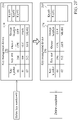
- FIGS. 2C and 2D are schematic views of an operation of reading a key, according to one embodiment of the present invention.
- the key management device 170 receives a key number of the to-be-read key from the encryption/decryption device 180 or the processor chip 110 .
- the key management device 170 can search the key corresponding to the key number from the key database, and also can determine, according to the metadata of the to-be-read key, whether the device or the user wanting to read the key meets the permission or privilege level recorded by the metadata of the to-be-read key, and further check whether the revoke attribute of the to-be-read key is set or asserted, and further check whether the current booting state of the control system 10 matches the booting state attribute of the metadata of the key attribute.
- the key management device 170 determines that the key is unable to read, and reports a read failure message to the device which wants to read the key.
- the key management device 170 can report the key and a read complete message, to the device which wants to read the key, and the operation of reading the key is completed. When any of these conditions is not met, the key management device 170 reports the key read failure message to the device which wants to read the key.
- the processor chip 110 can transmit the key number, which is the key number 00 , of the to-be-read key, to the key management device 170 .
- the key management device 170 searches the metadata related to the key number 00 , in the key lookup table of the register 174 , and checks whether the processor chip 110 is the owner of the key number 00 .
- the key management device 170 confirms that the processor chip 110 is actually the owner of the key number 00
- the key management device 170 reports a read complete message and the content of the key corresponding to the key number 00 , to the processor chip 110 .
- the key management device 170 first searches for the associated metadata of key 02 from the key lookup table in the register 174 , and confirms whether the AES encryption/decryption circuit 181 is the owner of key 02 .
- the encryption/decryption circuits 181 to 185 transmits the key read command to the key management device 170 through the corresponding bypass channel, it has also transmits the status of the encryption/decryption circuit itself (e.g., security level, privilege level, etc.) to the key management device 170 through the corresponding bypass channel.
- the key management device 170 determines that the AES encryption/decryption circuits 181 is indeed the owner of the key 02 and the metadata matches, the key management device 170 can directly transmit the key content corresponding to key 02 to the AES encryption/decryption circuit 181 through the bypass channel 1801 . Then, the AES encryption/decryption circuit 181 can perform decryption of the obtained key. In the embodiment, the flow for reading the key needs not to pass through the bus 21 , thereby improving the security of the system while keeping the key.
- FIGS. 2E and 2F are schematic views of an operation of deleting a key, according to one embodiment of the present invention.
- the user when the user determines that a specific key stored in the key management device 170 is already no longer used for the user, the user can send a single-key erase or delete command and the be-to-erased key number, to the key management device 170 via the processor chip 110 .
- the key management device 170 determines that the key erase command is a valid command sent by the processor chip 110 , the key management device 170 deletes the to-be-erased key from the corresponding storage space of the key database, and reports successful delete message to the processor chip 110 , as shown in FIG. 2E .
- the key management device 170 can obtain the key number, the key size and the storage location of the to-be-erased key from the key lookup table of the register 174 , and then calculate the storage space and range occupied by the to-be-erased key.
- the control circuit 171 of the key management device 170 can delete all data stored in the storage space corresponding to the to-be-erased key, and update the key lookup table in the register 174 and calculate the remaining space of each storage space of the key database again, as shown in FIG. 2F .
- the key management device 170 determines that the to-be-erased key contained in the erase command is stored in the OTP memory, the key management device 170 is unable to modify or delete the data stored in the OTP memory. At this time, the key management device 170 can set the revoke attribute field of the metadata related to the key number 01 in the key lookup table of the register 174 , to indicate that the key corresponding to the key number 01 is already revoked persistently and unable to be read or used.
- the user can send an all-key erase command to the key management device 170 upon requirement, via the processor chip 110 , to control the key management device 170 to delete all keys, and all storage spaces other than the OTP memory are released to the initial states.
- the processor chip 110 does not need to send the key number to be erased
- the key management device 170 can have an independent reset signal, and each time after the key management device 170 is reset, the key management device 170 should be initialized. For example, each time after the key management device 170 is reset, the content of the register 174 is also cleared, so the control circuit 171 must rebuild the key lookup table originally stored in the register 174 according to the data stored in different nonvolatile memory. For example, the control circuit 171 can read the key lookup table backed up in the OTP memory and the flash memory, and/or read the metadata, which corresponds to the stored keys, from the OTP memory and the flash memory.
- the metadata, corresponding to the keys, of the backup key lookup table may not be the latest metadata, so the control circuit 171 can read, from the OTP memory and the flash memory, the metadata corresponding to the stored keys, so as to update the key lookup table. After the control circuit 171 rebuilds the key lookup table, it indicates that the key management device 170 is initialized completely, so the user can start to use the key management device 170 . Furthermore, when the key management device 170 is not completely initialized, any operation related to key are regarded as an invalid operation by the key management device 170 .
- the control system 10 comprises a tamper detection circuit configured to detect whether the control system 10 is attacked or the data is tampered.
- the tamper detection circuit detects that the control system 10 is attacked or the data is tampered, the tamper detection circuit transmits a detection signal to the key management device 170 , and the key management device 170 then starts to remove all keys and related data, which includes backup data related to the keys, stored in the key management device 170 according to the detection signal.
- the key management device 170 is recovered to the initial state.
- FIG. 3 is a schematic view of a flowchart of creating a new key by a key management device, according to one embodiment of the present invention.
- step S 302 the key management device 170 enters the ready state. For example, after being powered on and reset, the key management device 170 is initialized first, and then enters the ready state after the initialization is completed, so as to receive different key operation commands.
- step S 304 the key management device 170 receives a key creation command.
- the key creation command can be from the central processing unit 111 .
- step S 306 the key management device 170 checks the remaining space of the key database.
- the key management device 170 can check the remaining spaces of different storage spaces of the key database, such as the remaining spaces of the SRAM 175 , the flash memory 113 and the OTP memory 114 .
- step S 308 the key management device 170 determines whether the remaining space is larger than or equal to the key size of the key to be created.
- step S 310 is executed; otherwise, step S 318 is executed.
- the key management device 170 can determine whether the remaining space is larger than or equal to the key size of the key to be created and also determine whether the key database reaches the upper limit of the key storage amount already.
- step S 310 is executed.
- step S 318 is executed.
- step S 310 the key management device 170 writes the metadata of the key into the key lookup table.
- the attributes of the metadata of the new key written into the key lookup table can include key size, owner, security level, privilege level, readable attribute, booting state and storage location of the to-be-created key.
- step S 312 the key management device 170 adds the key number of the new key in the key lookup table.
- the control circuit 171 of the key management device 170 can search for the key number that has not been used yet from number 0 in ascending order, and then use the minimum key number that has not been used yet, as the key number of the new key.
- the key management device 170 writes the new key into the key database.
- the key management device 170 can store the new key in the OTP memory of the key database according to the security level or privilege level set in the metadata of the new key.
- the key management device 170 can store the new key in the SRAM 175 or the flash memory 113 of the key database.
- step S 316 the key management device 170 reports the key number and the write complete message to the central processing unit 111 .
- step S 318 the key management device 170 reports the write failure message to the central processing unit 111 .
- step S 320 the key creation command is completed, and the flow returns to the step S 302 .
- the present invention provides a key management device for data encryption/decryption and a processor chip, and the key management device can determine the storage location of each key in the key database according to the key size and the current state (such as security state or remaining space) and automatically determine whether the remaining space of the storage location is enough to store the key with the set size. After the key is stored successfully, the key management device transmits the key number to the user, so that the user can read or delete the key according to the key number, without additionally recording the storage location of the key or other information related to the key.
- the key management device can determine the storage location of each key in the key database according to the key size and the current state (such as security state or remaining space) and automatically determine whether the remaining space of the storage location is enough to store the key with the set size. After the key is stored successfully, the key management device transmits the key number to the user, so that the user can read or delete the key according to the key number, without additionally recording the storage location of the key or other information related to the key.
- the key management device of the present invention must be initialized after every reset operation, so as to prevent the key data from being tampered possibly; furthermore, the key management device of the present invention can remove all stored keys according to the tamper detection signal, so as to ensure the security of key management.
- the key management device and the encryption/decryption device in the present invention are independent hardware circuits, and there are multiple bypass channels between these two devices for direct communication.
- the key management device can directly transmit the key to the corresponding encryption/decryption circuit through the bypass channel without passing through the bus, which can further improve the security of the control system to avoid the risk of the bus being eavesdropped and exposing the key.
Landscapes
- Engineering & Computer Science (AREA)
- Theoretical Computer Science (AREA)
- Computer Security & Cryptography (AREA)
- Computer Networks & Wireless Communication (AREA)
- Signal Processing (AREA)
- Physics & Mathematics (AREA)
- General Physics & Mathematics (AREA)
- Computer Hardware Design (AREA)
- General Engineering & Computer Science (AREA)
- Computing Systems (AREA)
- Microelectronics & Electronic Packaging (AREA)
- Power Engineering (AREA)
- Mathematical Physics (AREA)
- Software Systems (AREA)
- Algebra (AREA)
- Mathematical Analysis (AREA)
- Mathematical Optimization (AREA)
- Pure & Applied Mathematics (AREA)
- Storage Device Security (AREA)
Abstract
Description
Claims (10)
Applications Claiming Priority (2)
| Application Number | Priority Date | Filing Date | Title |
|---|---|---|---|
| TW108132364A TWI731407B (en) | 2019-09-09 | 2019-09-09 | Key management device having bypass channels and processor chip |
| TW108132364 | 2019-09-09 |
Publications (2)
| Publication Number | Publication Date |
|---|---|
| US20210075609A1 US20210075609A1 (en) | 2021-03-11 |
| US11368302B2 true US11368302B2 (en) | 2022-06-21 |
Family
ID=74806979
Family Applications (1)
| Application Number | Title | Priority Date | Filing Date |
|---|---|---|---|
| US17/014,767 Active 2040-12-25 US11368302B2 (en) | 2019-09-09 | 2020-09-08 | Key management device and processor chip having bypass channels |
Country Status (3)
| Country | Link |
|---|---|
| US (1) | US11368302B2 (en) |
| CN (1) | CN112468300B (en) |
| TW (1) | TWI731407B (en) |
Families Citing this family (4)
| Publication number | Priority date | Publication date | Assignee | Title |
|---|---|---|---|---|
| US12353335B2 (en) * | 2021-11-15 | 2025-07-08 | Samsung Electronics Co., Ltd. | Semiconductor device and method of operating the same |
| CN115098876B (en) * | 2022-06-29 | 2026-03-06 | 得一微电子股份有限公司 | Main controller chip, solid-state drive and its key management method, computer storage media |
| TWI825997B (en) | 2022-09-16 | 2023-12-11 | 瑞昱半導體股份有限公司 | Programmable secure management device and control method for performing key forwarding between secure devices |
| TWI833533B (en) * | 2022-12-30 | 2024-02-21 | 新唐科技股份有限公司 | Key management device, processor chip and method for avoid using incomplete keys |
Citations (11)
| Publication number | Priority date | Publication date | Assignee | Title |
|---|---|---|---|---|
| US20040123123A1 (en) * | 2002-12-18 | 2004-06-24 | Buer Mark L. | Methods and apparatus for accessing security association information in a cryptography accelerator |
| TW200415506A (en) | 2002-01-16 | 2004-08-16 | Infineon Technologies Ag | Calculating unit and method for performing an arithmetic operation with encrypted operands |
| US20040205331A1 (en) * | 2003-04-12 | 2004-10-14 | Hussain Muhammad Raghib | Apparatus and method for allocating resources within a security processing architecture using multiple groups |
| US7318160B2 (en) * | 2002-02-01 | 2008-01-08 | Hewlett-Packard Development Company, L.P. | Cryptographic key setup in queued cryptographic systems |
| TW200834375A (en) | 2007-01-30 | 2008-08-16 | Technology Properties Ltd | System and method of storage device data encryption and data access via a hardware key |
| US20080263269A1 (en) | 2007-04-18 | 2008-10-23 | Aviran Kadosh | Key selection device and process for content-addressable memory |
| US8213620B1 (en) | 2008-11-17 | 2012-07-03 | Netapp, Inc. | Method for managing cryptographic information |
| US20130275656A1 (en) | 2012-04-17 | 2013-10-17 | Fusion-Io, Inc. | Apparatus, system, and method for key-value pool identifier encoding |
| US20150043729A1 (en) | 2013-08-08 | 2015-02-12 | Vinodh Gopal | Instruction and logic to provide a secure cipher hash round functionality |
| TW201923595A (en) | 2017-10-30 | 2019-06-16 | 美商高通公司 | Memory access management for low-power use cases of a system on chip via secure non-volatile random access memory |
| US11184164B2 (en) * | 2018-02-02 | 2021-11-23 | Microsoft Technology Licensing, Llc | Secure crypto system attributes |
Family Cites Families (3)
| Publication number | Priority date | Publication date | Assignee | Title |
|---|---|---|---|---|
| CN105868643A (en) * | 2015-01-19 | 2016-08-17 | 群联电子股份有限公司 | Data protection method, memory control circuit unit and memory storage device |
| CN106156632B (en) * | 2015-05-17 | 2019-10-29 | 新唐科技股份有限公司 | Security device, method for providing security service to host in security device and security equipment |
| US20170126414A1 (en) * | 2015-10-28 | 2017-05-04 | Texas Instruments Incorporated | Database-less authentication with physically unclonable functions |
-
2019
- 2019-09-09 TW TW108132364A patent/TWI731407B/en active
- 2019-12-27 CN CN201911372406.1A patent/CN112468300B/en active Active
-
2020
- 2020-09-08 US US17/014,767 patent/US11368302B2/en active Active
Patent Citations (11)
| Publication number | Priority date | Publication date | Assignee | Title |
|---|---|---|---|---|
| TW200415506A (en) | 2002-01-16 | 2004-08-16 | Infineon Technologies Ag | Calculating unit and method for performing an arithmetic operation with encrypted operands |
| US7318160B2 (en) * | 2002-02-01 | 2008-01-08 | Hewlett-Packard Development Company, L.P. | Cryptographic key setup in queued cryptographic systems |
| US20040123123A1 (en) * | 2002-12-18 | 2004-06-24 | Buer Mark L. | Methods and apparatus for accessing security association information in a cryptography accelerator |
| US20040205331A1 (en) * | 2003-04-12 | 2004-10-14 | Hussain Muhammad Raghib | Apparatus and method for allocating resources within a security processing architecture using multiple groups |
| TW200834375A (en) | 2007-01-30 | 2008-08-16 | Technology Properties Ltd | System and method of storage device data encryption and data access via a hardware key |
| US20080263269A1 (en) | 2007-04-18 | 2008-10-23 | Aviran Kadosh | Key selection device and process for content-addressable memory |
| US8213620B1 (en) | 2008-11-17 | 2012-07-03 | Netapp, Inc. | Method for managing cryptographic information |
| US20130275656A1 (en) | 2012-04-17 | 2013-10-17 | Fusion-Io, Inc. | Apparatus, system, and method for key-value pool identifier encoding |
| US20150043729A1 (en) | 2013-08-08 | 2015-02-12 | Vinodh Gopal | Instruction and logic to provide a secure cipher hash round functionality |
| TW201923595A (en) | 2017-10-30 | 2019-06-16 | 美商高通公司 | Memory access management for low-power use cases of a system on chip via secure non-volatile random access memory |
| US11184164B2 (en) * | 2018-02-02 | 2021-11-23 | Microsoft Technology Licensing, Llc | Secure crypto system attributes |
Non-Patent Citations (2)
| Title |
|---|
| Bossuet et al, Architectures of flexible symmetric key crypto engines—a survey: From hardware coprocessor to multi-crypto-processor system on chip, ACM, 2013. * |
| Office Action dated Jul. 9, 2021 in U.S. Appl. No. 16/731,744, 17 pages. |
Also Published As
| Publication number | Publication date |
|---|---|
| TW202111584A (en) | 2021-03-16 |
| TWI731407B (en) | 2021-06-21 |
| CN112468300A (en) | 2021-03-09 |
| CN112468300B (en) | 2023-07-04 |
| US20210075609A1 (en) | 2021-03-11 |
Similar Documents
| Publication | Publication Date | Title |
|---|---|---|
| US11329815B2 (en) | Key management device and processor chip for data encryption/decryption | |
| US11374967B2 (en) | Systems and methods for detecting replay attacks on security space | |
| US11368302B2 (en) | Key management device and processor chip having bypass channels | |
| US11651061B2 (en) | Memory controller and storage device including the same | |
| US11194920B2 (en) | File system metadata protection | |
| US10503934B2 (en) | Secure subsystem | |
| CN111177807B (en) | Data storage device, method of operating the same, and storage system having the same | |
| US20100058066A1 (en) | Method and system for protecting data | |
| JP2020119298A (en) | Memory system | |
| US20180260151A1 (en) | Data Storage Device and Operating Method Therefor | |
| TW201807616A (en) | Safe storage system and method for safe storage | |
| CN108985111A (en) | Data storage device and firmware encryption and decryption method | |
| US11644983B2 (en) | Storage device having encryption | |
| KR20230082807A (en) | Storage controller and operation method of electronic system | |
| Zhang et al. | Ensuring data confidentiality via plausibly deniable encryption and secure deletion–a survey | |
| KR100678927B1 (en) | How to assign a security zone to an insecure zone and a portable storage device providing the same | |
| US20150227755A1 (en) | Encryption and decryption methods of a mobile storage on a file-by-file basis | |
| US20230208821A1 (en) | Method and device for protecting and managing keys | |
| TW201830284A (en) | Data storage system, data storage method and data read method | |
| CN117407327A (en) | Storage device with RPMB reset function and RPMB management method thereof | |
| TWI833533B (en) | Key management device, processor chip and method for avoid using incomplete keys | |
| US12314190B2 (en) | Micro-controller chip and access method thereof | |
| GB2434887A (en) | Access control by encrypting stored data with a key based on a "fingerprint" of the device storing the data | |
| CN117708900A (en) | Storage device, method of operating the same, and method of operating electronic device including the same | |
| CN120850369A (en) | Method for securely managing storage devices |
Legal Events
| Date | Code | Title | Description |
|---|---|---|---|
| FEPP | Fee payment procedure |
Free format text: ENTITY STATUS SET TO UNDISCOUNTED (ORIGINAL EVENT CODE: BIG.); ENTITY STATUS OF PATENT OWNER: LARGE ENTITY |
|
| AS | Assignment |
Owner name: NUVOTON TECHNOLOGY CORPORATION, TAIWAN Free format text: ASSIGNMENT OF ASSIGNORS INTEREST;ASSIGNOR:LI, YU-SHAN;REEL/FRAME:053776/0940 Effective date: 20200903 |
|
| STPP | Information on status: patent application and granting procedure in general |
Free format text: APPLICATION DISPATCHED FROM PREEXAM, NOT YET DOCKETED |
|
| STPP | Information on status: patent application and granting procedure in general |
Free format text: DOCKETED NEW CASE - READY FOR EXAMINATION |
|
| STPP | Information on status: patent application and granting procedure in general |
Free format text: NOTICE OF ALLOWANCE MAILED -- APPLICATION RECEIVED IN OFFICE OF PUBLICATIONS |
|
| STPP | Information on status: patent application and granting procedure in general |
Free format text: PUBLICATIONS -- ISSUE FEE PAYMENT RECEIVED |
|
| STPP | Information on status: patent application and granting procedure in general |
Free format text: PUBLICATIONS -- ISSUE FEE PAYMENT VERIFIED |
|
| STCF | Information on status: patent grant |
Free format text: PATENTED CASE |
|
| MAFP | Maintenance fee payment |
Free format text: PAYMENT OF MAINTENANCE FEE, 4TH YEAR, LARGE ENTITY (ORIGINAL EVENT CODE: M1551); ENTITY STATUS OF PATENT OWNER: LARGE ENTITY Year of fee payment: 4 |