US11368106B2 - Power converter PWM - Google Patents
Power converter PWM Download PDFInfo
- Publication number
- US11368106B2 US11368106B2 US16/823,676 US202016823676A US11368106B2 US 11368106 B2 US11368106 B2 US 11368106B2 US 202016823676 A US202016823676 A US 202016823676A US 11368106 B2 US11368106 B2 US 11368106B2
- Authority
- US
- United States
- Prior art keywords
- signal
- triangle carrier
- triangle
- power
- phase
- Prior art date
- Legal status (The legal status is an assumption and is not a legal conclusion. Google has not performed a legal analysis and makes no representation as to the accuracy of the status listed.)
- Active, expires
Links
Images


Classifications
-
- H—ELECTRICITY
- H02—GENERATION; CONVERSION OR DISTRIBUTION OF ELECTRIC POWER
- H02M—APPARATUS FOR CONVERSION BETWEEN AC AND AC, BETWEEN AC AND DC, OR BETWEEN DC AND DC, AND FOR USE WITH MAINS OR SIMILAR POWER SUPPLY SYSTEMS; CONVERSION OF DC OR AC INPUT POWER INTO SURGE OUTPUT POWER; CONTROL OR REGULATION THEREOF
- H02M7/00—Conversion of AC power input into DC power output; Conversion of DC power input into AC power output
- H02M7/42—Conversion of DC power input into AC power output without possibility of reversal
- H02M7/44—Conversion of DC power input into AC power output without possibility of reversal by static converters
- H02M7/48—Conversion of DC power input into AC power output without possibility of reversal by static converters using discharge tubes with control electrode or semiconductor devices with control electrode
- H02M7/53—Conversion of DC power input into AC power output without possibility of reversal by static converters using discharge tubes with control electrode or semiconductor devices with control electrode using devices of a triode or transistor type requiring continuous application of a control signal
- H02M7/537—Conversion of DC power input into AC power output without possibility of reversal by static converters using discharge tubes with control electrode or semiconductor devices with control electrode using devices of a triode or transistor type requiring continuous application of a control signal using semiconductor devices only, e.g. single switched pulse inverters
- H02M7/5387—Conversion of DC power input into AC power output without possibility of reversal by static converters using discharge tubes with control electrode or semiconductor devices with control electrode using devices of a triode or transistor type requiring continuous application of a control signal using semiconductor devices only, e.g. single switched pulse inverters in a bridge configuration
- H02M7/53871—Conversion of DC power input into AC power output without possibility of reversal by static converters using discharge tubes with control electrode or semiconductor devices with control electrode using devices of a triode or transistor type requiring continuous application of a control signal using semiconductor devices only, e.g. single switched pulse inverters in a bridge configuration with automatic control of output voltage or current
-
- H—ELECTRICITY
- H02—GENERATION; CONVERSION OR DISTRIBUTION OF ELECTRIC POWER
- H02M—APPARATUS FOR CONVERSION BETWEEN AC AND AC, BETWEEN AC AND DC, OR BETWEEN DC AND DC, AND FOR USE WITH MAINS OR SIMILAR POWER SUPPLY SYSTEMS; CONVERSION OF DC OR AC INPUT POWER INTO SURGE OUTPUT POWER; CONTROL OR REGULATION THEREOF
- H02M1/00—Details of apparatus for conversion
- H02M1/44—Circuits or arrangements for compensating for electromagnetic interference in converters or inverters
-
- H—ELECTRICITY
- H02—GENERATION; CONVERSION OR DISTRIBUTION OF ELECTRIC POWER
- H02M—APPARATUS FOR CONVERSION BETWEEN AC AND AC, BETWEEN AC AND DC, OR BETWEEN DC AND DC, AND FOR USE WITH MAINS OR SIMILAR POWER SUPPLY SYSTEMS; CONVERSION OF DC OR AC INPUT POWER INTO SURGE OUTPUT POWER; CONTROL OR REGULATION THEREOF
- H02M1/00—Details of apparatus for conversion
- H02M1/12—Arrangements for reducing harmonics from AC input or output
- H02M1/126—Arrangements for reducing harmonics from AC input or output using passive filters
-
- H—ELECTRICITY
- H02—GENERATION; CONVERSION OR DISTRIBUTION OF ELECTRIC POWER
- H02M—APPARATUS FOR CONVERSION BETWEEN AC AND AC, BETWEEN AC AND DC, OR BETWEEN DC AND DC, AND FOR USE WITH MAINS OR SIMILAR POWER SUPPLY SYSTEMS; CONVERSION OF DC OR AC INPUT POWER INTO SURGE OUTPUT POWER; CONTROL OR REGULATION THEREOF
- H02M7/00—Conversion of AC power input into DC power output; Conversion of DC power input into AC power output
- H02M7/42—Conversion of DC power input into AC power output without possibility of reversal
- H02M7/44—Conversion of DC power input into AC power output without possibility of reversal by static converters
- H02M7/48—Conversion of DC power input into AC power output without possibility of reversal by static converters using discharge tubes with control electrode or semiconductor devices with control electrode
- H02M7/53—Conversion of DC power input into AC power output without possibility of reversal by static converters using discharge tubes with control electrode or semiconductor devices with control electrode using devices of a triode or transistor type requiring continuous application of a control signal
- H02M7/537—Conversion of DC power input into AC power output without possibility of reversal by static converters using discharge tubes with control electrode or semiconductor devices with control electrode using devices of a triode or transistor type requiring continuous application of a control signal using semiconductor devices only, e.g. single switched pulse inverters
- H02M7/539—Conversion of DC power input into AC power output without possibility of reversal by static converters using discharge tubes with control electrode or semiconductor devices with control electrode using devices of a triode or transistor type requiring continuous application of a control signal using semiconductor devices only, e.g. single switched pulse inverters with automatic control of output wave form or frequency
- H02M7/5395—Conversion of DC power input into AC power output without possibility of reversal by static converters using discharge tubes with control electrode or semiconductor devices with control electrode using devices of a triode or transistor type requiring continuous application of a control signal using semiconductor devices only, e.g. single switched pulse inverters with automatic control of output wave form or frequency by pulse-width modulation
-
- H—ELECTRICITY
- H02—GENERATION; CONVERSION OR DISTRIBUTION OF ELECTRIC POWER
- H02P—CONTROL OR REGULATION OF ELECTRIC MOTORS, ELECTRIC GENERATORS OR DYNAMO-ELECTRIC CONVERTERS; CONTROLLING TRANSFORMERS, REACTORS OR CHOKE COILS
- H02P27/00—Arrangements or methods for the control of AC motors characterised by the kind of supply voltage
- H02P27/04—Arrangements or methods for the control of AC motors characterised by the kind of supply voltage using variable-frequency supply voltage, e.g. inverter or converter supply voltage
- H02P27/06—Arrangements or methods for the control of AC motors characterised by the kind of supply voltage using variable-frequency supply voltage, e.g. inverter or converter supply voltage using DC to AC converters or inverters
- H02P27/08—Arrangements or methods for the control of AC motors characterised by the kind of supply voltage using variable-frequency supply voltage, e.g. inverter or converter supply voltage using DC to AC converters or inverters with pulse width modulation
Definitions
- the present disclosure relates to power converters and more particularly, to pulse width modulation controllers of a power converter or aerospace motor controller.
- Power converters including, for example motor controllers, have a filter that uses a common mode inductor.
- the filter is configured to reduce harmonics generated by switching that occurs within the power converter and to reduce EMI radiation.
- Ten-thirty percent of the size and weight of the power converter can be attributed to the common mode inductor.
- a higher switching frequency is used. This option increases switching losses and burdens a cooling system responsible for cooling the power converter.
- the converter is provided with multilevel inverters or interleaved inverters, which complicates circuit topology and control of the converter, in addition to the for significantly more semiconductor switches.
- the filter is an active filter or additional switching poles are provided to actively offset the harmonics generated by the converter's inverter. However, this option further complicates circuit topology and control of the converter, in addition to the for significantly more semiconductor switches.
- a pulse width modulator (PWM) of a multi-phase power converter includes a signal modulator that corresponds to each phase of the converter.
- Each signal modulator of the PWM is configured to receive a unique triangle carrier signal, receive a unique sine wave signal, compare the received triangle carrier signal and the received sine wave signal, and output at least one control signal based on a result of the comparison.
- the control signal controls an inverter that applies pulse width modulation to a DC power for converting the DC power to a multi-phase power, AC harmonics of the multi-phase power being filtered by a common mode inductor.
- the PWM can further include a different triangle wave generator for each of the signal modulators, each triangle wave generator configured to generate one of the unique triangle carrier signals.
- the multi-phase convertor can have n phases, the triangle carrier signals can have the same cycle, and each of the triangle carrier signals can be shifted by 1/n of the cycle so that each triangle carrier signal is shifted relative to all of the other triangle carrier signals.
- the triangle carrier signals can be shifted by a forward rotational shift.
- the triangle carrier signals can be shifted by a backward rotational shift.
- a multi-phase power converter includes an inverter configured to apply pulse width modulation to a DC power from a DC power source for converting the DC power to a multi-phase power and a filter configured to filter AC harmonics of the multi-phase power.
- the filter includes a common mode inductor for the multi-phase power.
- the power converter further includes a PWM controller having a signal modulator that corresponds to each phase of the multi-phase converter or controller.
- Each signal modulator of the PWM is configured to receive a unique triangle carrier signal, receive a unique sine wave signal, compare the received triangle carrier signal and the received sine wave signal, and output at least one control signal based on a result of the comparison, wherein the control signal controls pulse width modulation of the DC power.
- the PWM can further include a different triangle wave generator for each of the signal modulators, each triangle wave generator configured to generate one of the unique triangle carrier signals.
- the multi-phase power can have n phases, the triangle carrier signals have the same cycle, and each of the triangle carrier signals can be shifted by 1/n of the cycle so that each triangle carrier signal can be shifted relative to all of the other triangle carrier signals.
- the triangle carrier signals can be shifted by a forward rotational shift or a backward rotational shift.
- a core size of a core of each common mode inductor can be reduced by at least about 50% in at least one of size and weight relative to a configuration with a PWM in which all of the signal modulators are configured to receive the same triangle carrier signal.
- a core size of a core of each common mode inductor can be reduced by about 65% in at least one of size and weight relative to a configuration with a PWM in which all of the signal modulators are configured to receive the same triangle carrier signal.
- the filter can further include a differential inductor, wherein a size and weight of the differential inductor and a winding of the common mode inductor can be substantially unchanged relative to a configuration with a PWM in which all of the signal modulators are configured to receive the same triangle carrier signal.
- the PWM can be retrofitted to the convertor to replace a PWM that is configured for all of the signal modulators to receive the same triangle carrier signal.
- the filter can further include a differential inductor.
- a size and weight of the differential inductor can be substantially unchanged relative to a configuration with a PWM in which all of the signal modulators are configured to receive the same triangle carrier signal.
- a method of controlling a pulse width modulation of a DC power converted into a multi-phase power includes, for each phase power of the multi-phase power, receiving a unique triangle carrier signal, receiving a unique sine wave signal, comparing the received triangle carrier signal and the received sine wave signal, outputting at least one control signal based on a result of the comparison, and controlling by the control signal pulse width modulation of the DC power for converting the DC power to the multi-phase power, AC harmonics of the multi-phase power being filtered using common mode inductance.
- the method can further include generating the unique triangle carrier signals.
- the multi-phase power can have n phases
- the triangle carrier signals can have the same cycle
- the method can further include shifting each of the triangle carrier signals by 1/n of the cycle so that each triangle carrier signal is shifted relative to all of the other triangle carrier signals.
- the method can further include replacing a component that was previously generating the same triangle carrier signal for each phase power that corresponds to each phase of the multi-phase with a component generating the unique triangle carrier signals.
- the method can further include reducing in at least one of size and weigh by at least about 50% a core size of a core of each common mode inductor filtering the multi-phase signal before it is provided to the motor relative to a configuration in which the same triangle carrier signal is received for each phase power.
- the method can further include maintaining substantially the same size and weight of a differential inductor and winding of a common mode inductor that filter the multi-phase power before it is provided to the motor relative to a configuration in which the same triangle carrier signal is received for each phase power.
- FIG. 1 shows a schematic diagram of an example power converter in accordance with one or more embodiments of the disclosure
- FIG. 2 shows a schematic diagram of a common mode (CM) inductor of a power converter, in accordance with one or more embodiments of the disclosure
- FIG. 3 shows a schematic diagram of a pulse width modulation (PWM) of a power converter, in accordance with one or more embodiments of the disclosure
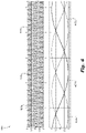
- FIG. 4 shows a plot of example sine wave signals and triangle carrier signals generated for each of the signal modulator of a PWM controller, in accordance with one or more embodiments of the disclosure
- FIG. 5 shows example plots of spectra of a conventional sine-triangle PWM controlled inverter
- FIG. 6 shows example plots of spectra of a forward rotational carrier shifted PWM controlled inverter controlled using PWM shown in FIG. 3 ;
- FIG. 7 shows example plots of spectra of a backward rotational carrier shifted PWM controlled inverter controlled using PWM shown in FIG. 3 ;
- FIG. 8 shows a schematic block diagram of an example computing system, in accordance with an illustrative embodiment of the present disclosure.
- FIG. 1 depicts an exemplary power converter 100 in which below illustrated embodiments may be implemented.
- the power converter is a controller for a motor 10 (e.g., an aerospace motor), however the disclosure is applicable to any power converter that includes an inverter with switches controlled by a pulse width modulator (PWM) and that includes a filter having at least one common mode inductor.
- PWM pulse width modulator
- Power converter 100 includes an inverter 104 receiving a DC power via signal paths 103 a and 103 b from a DC power source 106 .
- the converter 100 further includes a pulse width modulator (PWM) 102 and a control module 114 .
- PWM 102 converts commands from control module 114 to switch logic that can control the switches of inverter 104 .
- Control module 114 controls PWM 102 .
- Control module 114 can include a digital processing device, such as a microprocessor, digital signal processor (DSP), field programmable gate array (FPGA), application specific integrated circuit (ASIC), programmable integrated circuit (IC), for example.
- DSP digital signal processor
- FPGA field programmable gate array
- ASIC application specific integrated circuit
- IC programmable integrated circuit
- PWM 102 can also be implemented digitally, such as by a digital processing device (e.g., a microprocessor, DSP, FPGA, ASIC, programmable IC.
- PWM 102 can be integrated with control module 114 .
- PWM 102 can be implemented by hardware, such as by a digital or analog circuit.
- the inverter 104 modulates the DC power received from the DC power source and outputs a multi-phase power via phase paths 105 a - 105 c , such as to a motor 10 .
- Inverter 104 can include, for example and without limitation to a specific inverter topology, a six-switch inverter topology. Inverter 104 can include two levels or higher levels, although the benefit of this invention is most significant at lower levels.
- the converter 100 includes a filter 108 that includes a differential-mode (DM) inductor 110 disposed along each respective phase path 105 a - 105 c , and a common-mode (CM) inductor 112 disposed along each respective phase path 105 a - 105 c .
- DM differential-mode
- CM common-mode
- CM inductor 112 includes a magnetic core 202 and a winding 204 having coils that carry the corresponding phase of the multi-phase power output by inverter 104 and filtered by DM inductor 110 .
- Winding 204 is formed of a highly conductive material, such as copper.
- the size and weight of the winding 204 needs to be sufficient to support phase currents, which are proportional to Vdiff, the differential voltage component measured at lines 105 a , 105 b , or 105 c .
- Magnetic core 202 of the common mode inductor carries common mode flux and need to be sufficient to support Vcom, which is the common mode voltage component measured as one third of sum of three phase voltages at output terminals of inverter 104 .
- Control module 114 is configured to reduce the Vcom at 1.0 pu of switch frequency by providing a separate triangle carriers to modulate each of the phase power input to inverter 104 (as shown in FIG. 1 ). For n phase power, the triangle carrier is shifted by 1/n of the carrier cycle.
- Control module 114 includes a different signal modulator for each respective phase of the multiphase power output by inverter 104 .
- the multiphase power is a three-phase power
- three signal modulators 302 are provided, one for each phase.
- Each signal modulator 302 includes a triangle wave generator 304 , a sine wave generator 306 , a comparator 308 , and an output buffer 310 .
- Triangle wave generator 304 generates a triangle carrier signal that is unique for the signal modulator 302 and phase to which it corresponds and provides the triangle carrier signal to comparator 308 .
- Sine wave generator 306 generates a sine wave signal that is unique for the signal modulator 302 and phase to which it corresponds and provides the sine wave signal to comparator 308 .
- Comparator 308 receives and compares the triangle carrier signal and sine wave signal output by the corresponding triangle wave generator 304 and sine wave generator 306 , respectively and outputs at least one control signal based on a result of the comparison.
- Output buffer 310 splits the three phase logic signals to six signals and buffers the control signal and outputs it to the six switches in inverter 104 (shown in FIG. 1 ) for converting the DC power to AC Power.
- Output buffer 310 can include a noninverting buffer and an inverting buffer. The output signals of each output buffer 310 is provided to a different switch in inverter 104 .
- an example plot 400 is shown of the sine wave signals and triangle carrier signals generated for each of the three signal modulators 302 that corresponds to a different phase of phase paths 105 a , 105 b , 105 c .
- Sine wave signal 402 a and triangle carrier signal 404 a correspond to phase path 105 a .
- Sine wave signal 402 b and triangle carrier signal 404 b correspond to phase path 105 b .
- Sine wave signal 402 c and triangle carrier signal 404 c correspond to phase path 105 c.
- Vdiff 506 1.0 pu amplitude at f close to 0 pu governs size of winding 204 (shown in FIG. 2 ).
- the lowest frequency common mode Vcom 510 governs size of core 202 (shown in FIG. 2 ).
- a differential mode plot 602 and a common mode plot 604 are similar to plots 502 and 504 , except that forward rotational carrier shifted PWM control is used.
- Vdiff 506 1.0 pu amplitude remains at f close to 0 pu.
- Spectral lines 509 and 510 have exchanged locations between top and bottom plots: spectral line 510 has now become differential mode and spectral line 509 has now become common mode. Their amplitude and frequency of spectral lines 508 - 510 remain the same.
- Spectral lines 509 Vcom in the disclosed PWM shown in FIG. 6 , and 510 Vcom of the conventional PWM shown in FIG. 5 , both at or close to (to the right of 1.0) f 1.0 pu, are compared, wherein spectral line 509 is reduced to less than 0.5 pu, which results in the common mode inductor core size 202 being reduced in size.
- a differential mode plot 702 and a common mode plot 704 are similar to plots 602 and 604 , except that backward rotational carrier shifted PWM control is used.
- Vdiff 506 1.0 pu at f close to 0 pu.
- Original spectral line 508 has been exchanged from being a differential component to becoming a common mode component.
- Original spectral line 510 which is greater than 0.5 has changed from common mode to differential mode, and spectral line, 508 ⁇ 0.5 has changed from differential mode to common mode, which results in the common mode inductor core size 202 being reduced in size as well.
- FIGS. 5-7 demonstrate that when triangle carrier signals are generated for each of the three signal modulators 302 that corresponds to a different phase of phase paths 105 a , 105 b , 105 c , for both forward rotation and backward rotation carrier shifts, common mode spectral line 510 is moved to differential mode. Also demonstrated is movement of one of the side band components of spectral lines 508 and 509 are moved from differential mode components to common mode components. In the forward rotational case shown in FIG. 6 , spectral line 509 is moved to the plot for common mode. In the backward rotational case shown in FIG. 7 , spectral line 508 is moved to the plot for common mode.
- spectral line 509 has a relatively higher frequency than spectral line 508 . Accordingly, forward rotation may provide a higher benefit, since higher frequency corresponds to lower Volt-second, hence greater reduction in inductor core size.
- Equation (1) A qualitative determination of the reduction to common mode inductor core size and winding size achievable by the carrier shifted PWM control is described by Equations (1) and (2), respectively:
- Cfe SUM( V/f ),for harmonics 1 through 15 Equation(1)
- Ccu SUM(( V/f ) ⁇ circumflex over ( ) ⁇ 2),for harmonics 1 through 15 Equation (2), wherein Cfe is a core size index, Ccu is a winding size index, V represents voltage spectrum magnitude, and f represents the frequency of each voltage spectrum component (represented as spectral lines).
- the disclosed carrier shifted PWM control can potentially reduce the common mode inductor core size by more than 50%.
- the inductor core size required to cover all modulation indices can be as low as only 45% of that relative to configurations using conventional PWM control.
- any negative impact on differential inductor size and weight was determined to be hardly noticeable negative relative to configurations using conventional PWM control.
- PWM 102 and control module 114 can be retrofitted to power converters (including motor controllers) that use conventional PWM control. Once retrofitted, no switching losses are incurred. The retrofit rather reduces the common mode inductor core flux density and reduces the common mode inductor core size in accordance with Equation (1).
- FIG. 8 a block diagram of an example computing system 800 is shown, which provides an example configuration of control module 114 .
- Computing system 800 is only one example of a suitable system and is not intended to suggest any limitation as to the scope of use or functionality of embodiments of the disclosure described herein.
- Computing system 800 can be implemented using hardware, software, and/or firmware. Regardless, computing system 800 is capable of being implemented and/or performing functionality as set forth in the disclosure.
- Computing system 800 is shown in the form of a general-purpose computing device.
- Computing system 800 includes a processing device 802 , memory 804 , an input/output (I/O) interface (I/F) 806 that can communicate with an internal component 810 , and optionally an external component 808 .
- I/O input/output
- I/F input/output interface
- the processing device 802 can include, for example, a programmable logic device (PLOD), microprocessor, digital signal processor (DSP), a microcontroller, a field programmable gate array (FPGA), an application specific integrated circuit (ASCI), and/or other discrete or integrated logic circuitry having similar processing capabilities.
- POD programmable logic device
- DSP digital signal processor
- FPGA field programmable gate array
- ASCI application specific integrated circuit
- the processing device 802 and the memory 804 can be included in components provided in the FPGA, ASCI, microcontroller, or microprocessor, for example.
- Memory 804 can include, for example, volatile and non-volatile memory for storing data temporarily or long term, and for storing programmable instructions executable by the processing device 802 .
- I/O I/F 806 can include an interface and/or conductors to couple to the one or more internal components 808 and/or external components 810 .
- These computer program instructions may also be stored in a computer readable medium that can direct a computer, other programmable data processing apparatus, or other devices to function in a particular manner, such that the instructions stored in the computer readable medium produce an article of manufacture including instructions which implement the function/act specified in the flow diagram and/or block diagram block or blocks.
- the computer program instructions may also be loaded onto a computer, other programmable data processing apparatus, or other devices to cause a series of operational operations to be performed on the computer, other programmable apparatus or other devices to produce a computer implemented process such that the instructions which execute on the computer or other programmable apparatus provide processes for implementing the functions/acts specified in the block diagram block or blocks.
- Embodiments of the controller 210 may be implemented or executed by one or more computer systems, such as a microprocessor.
- Each computer system 800 can implement controller 26 , or multiple instances thereof.
- computer system 800 may include one or more of a microprocessor, an FPGA, application specific integrated circuit (ASCI), microcontroller.
- the computer system 800 can be provided as an embedded device. All or portions of the computer system 800 can be provided externally, such by way of a mobile computing device, a smart phone, a desktop computer, a laptop, or the like.
- Computer system 800 is only one example of a suitable system and is not intended to suggest any limitation as to the scope of use or functionality of embodiments of the disclosure described herein. Regardless, computer system 800 is capable of being implemented and/or performing any of the functionality set forth hereinabove.
- Computer system 800 may be described in the general context of computer system-executable instructions, such as program modules, being executed by a computer system.
- program modules may include routines, programs, objects, components, logic, data structures, and so on that perform particular tasks or implement particular abstract data types.
Landscapes
- Engineering & Computer Science (AREA)
- Power Engineering (AREA)
- Physics & Mathematics (AREA)
- Electromagnetism (AREA)
- Inverter Devices (AREA)
Abstract
Description
Cfe=SUM(V/f),for
Ccu=SUM((V/f){circumflex over ( )}2),for
wherein Cfe is a core size index, Ccu is a winding size index, V represents voltage spectrum magnitude, and f represents the frequency of each voltage spectrum component (represented as spectral lines).
Claims (17)
Priority Applications (2)
| Application Number | Priority Date | Filing Date | Title |
|---|---|---|---|
| US16/823,676 US11368106B2 (en) | 2020-03-19 | 2020-03-19 | Power converter PWM |
| EP21162945.6A EP3883109A1 (en) | 2020-03-19 | 2021-03-16 | Power converter pwm |
Applications Claiming Priority (1)
| Application Number | Priority Date | Filing Date | Title |
|---|---|---|---|
| US16/823,676 US11368106B2 (en) | 2020-03-19 | 2020-03-19 | Power converter PWM |
Publications (2)
| Publication Number | Publication Date |
|---|---|
| US20210297010A1 US20210297010A1 (en) | 2021-09-23 |
| US11368106B2 true US11368106B2 (en) | 2022-06-21 |
Family
ID=74947014
Family Applications (1)
| Application Number | Title | Priority Date | Filing Date |
|---|---|---|---|
| US16/823,676 Active 2040-06-26 US11368106B2 (en) | 2020-03-19 | 2020-03-19 | Power converter PWM |
Country Status (2)
| Country | Link |
|---|---|
| US (1) | US11368106B2 (en) |
| EP (1) | EP3883109A1 (en) |
Citations (17)
| Publication number | Priority date | Publication date | Assignee | Title |
|---|---|---|---|---|
| JPS62171462A (en) | 1986-01-23 | 1987-07-28 | Fuji Electric Co Ltd | 3-phase noise filter for stationary power converter |
| US4843534A (en) * | 1987-11-13 | 1989-06-27 | Pacific Power Source Corp. | DC to AC switching converter with phased delayed parallel switchers |
| US4904919A (en) * | 1988-06-21 | 1990-02-27 | Allen-Bradley Company, Inc. | Dual mode control of a PWM motor drive for current limiting |
| US5657217A (en) * | 1994-03-02 | 1997-08-12 | Kabushiki Kaisha Yaskawa Denki | Multi-coupled power conversion system and control method for the same |
| US6605928B2 (en) | 1996-12-03 | 2003-08-12 | Elliott Energy Systems, Inc. | Electrical system for turbine/alternator on common shaft |
| KR20040057202A (en) | 2002-12-26 | 2004-07-02 | 김이훈 | Method for operating a three-phase induction motor drive system for common mode voltage reduction |
| US6801441B2 (en) | 2000-02-04 | 2004-10-05 | Ricotec Oy | Pulse width modulation frequency converter |
| US20040223348A1 (en) * | 2003-05-09 | 2004-11-11 | West Richard T. | Power converter with ripple current cancellation using skewed switching techniques |
| US20050179419A1 (en) | 2004-02-16 | 2005-08-18 | Vacon Oyj | Synchronization of parallel-connected inverter units or frequency converters |
| US7218072B2 (en) * | 2003-02-18 | 2007-05-15 | Matsushita Electric Industrial Co., Ltd. | Motor driving device, motor to be driven by the same device, and apparatus using the same motor |
| US7564164B2 (en) * | 2004-02-23 | 2009-07-21 | Nec Corporation | Drive circuit for piezoelectric pump and cooling system that uses this drive circuit |
| US7808125B1 (en) * | 2006-07-31 | 2010-10-05 | Sustainable Energy Technologies | Scheme for operation of step wave power converter |
| EP2408093A2 (en) | 2010-07-13 | 2012-01-18 | Eaton Aviation Corporation | Inverter filter including differential mode and common mode, and system including the same |
| US8264191B1 (en) | 2009-08-31 | 2012-09-11 | Indian Institute Of Science | Load commutated current source inverter |
| US20140015500A1 (en) * | 2012-07-12 | 2014-01-16 | Primarion, Inc. | Multiphase digital current mode controller with dynamic current allocation |
| US8712666B2 (en) | 2011-03-15 | 2014-04-29 | Loncin Motor Co., Ltd. | Multiple-frequency inversion method and control apparatus for internal combustion engine driven generator |
| CN108039815A (en) | 2017-12-15 | 2018-05-15 | 西安许继电力电子技术有限公司 | A kind of electromagnetic interference suppression circuit and its operating method |
-
2020
- 2020-03-19 US US16/823,676 patent/US11368106B2/en active Active
-
2021
- 2021-03-16 EP EP21162945.6A patent/EP3883109A1/en active Pending
Patent Citations (18)
| Publication number | Priority date | Publication date | Assignee | Title |
|---|---|---|---|---|
| JPS62171462A (en) | 1986-01-23 | 1987-07-28 | Fuji Electric Co Ltd | 3-phase noise filter for stationary power converter |
| US4843534A (en) * | 1987-11-13 | 1989-06-27 | Pacific Power Source Corp. | DC to AC switching converter with phased delayed parallel switchers |
| US4904919A (en) * | 1988-06-21 | 1990-02-27 | Allen-Bradley Company, Inc. | Dual mode control of a PWM motor drive for current limiting |
| US5657217A (en) * | 1994-03-02 | 1997-08-12 | Kabushiki Kaisha Yaskawa Denki | Multi-coupled power conversion system and control method for the same |
| US6605928B2 (en) | 1996-12-03 | 2003-08-12 | Elliott Energy Systems, Inc. | Electrical system for turbine/alternator on common shaft |
| US20040066177A1 (en) * | 1996-12-03 | 2004-04-08 | Gupta Suresh C. | Method and apparatus for monitoring turbine parameters of turbine/alternator on common shaft |
| US6801441B2 (en) | 2000-02-04 | 2004-10-05 | Ricotec Oy | Pulse width modulation frequency converter |
| KR20040057202A (en) | 2002-12-26 | 2004-07-02 | 김이훈 | Method for operating a three-phase induction motor drive system for common mode voltage reduction |
| US7218072B2 (en) * | 2003-02-18 | 2007-05-15 | Matsushita Electric Industrial Co., Ltd. | Motor driving device, motor to be driven by the same device, and apparatus using the same motor |
| US20040223348A1 (en) * | 2003-05-09 | 2004-11-11 | West Richard T. | Power converter with ripple current cancellation using skewed switching techniques |
| US20050179419A1 (en) | 2004-02-16 | 2005-08-18 | Vacon Oyj | Synchronization of parallel-connected inverter units or frequency converters |
| US7564164B2 (en) * | 2004-02-23 | 2009-07-21 | Nec Corporation | Drive circuit for piezoelectric pump and cooling system that uses this drive circuit |
| US7808125B1 (en) * | 2006-07-31 | 2010-10-05 | Sustainable Energy Technologies | Scheme for operation of step wave power converter |
| US8264191B1 (en) | 2009-08-31 | 2012-09-11 | Indian Institute Of Science | Load commutated current source inverter |
| EP2408093A2 (en) | 2010-07-13 | 2012-01-18 | Eaton Aviation Corporation | Inverter filter including differential mode and common mode, and system including the same |
| US8712666B2 (en) | 2011-03-15 | 2014-04-29 | Loncin Motor Co., Ltd. | Multiple-frequency inversion method and control apparatus for internal combustion engine driven generator |
| US20140015500A1 (en) * | 2012-07-12 | 2014-01-16 | Primarion, Inc. | Multiphase digital current mode controller with dynamic current allocation |
| CN108039815A (en) | 2017-12-15 | 2018-05-15 | 西安许继电力电子技术有限公司 | A kind of electromagnetic interference suppression circuit and its operating method |
Non-Patent Citations (1)
| Title |
|---|
| Extended European Search Report for European Patent Application No. EP21162945.6, dated Jul. 28, 2021. |
Also Published As
| Publication number | Publication date |
|---|---|
| EP3883109A1 (en) | 2021-09-22 |
| US20210297010A1 (en) | 2021-09-23 |
Similar Documents
| Publication | Publication Date | Title |
|---|---|---|
| Trinh et al. | An advanced current control strategy for three-phase shunt active power filters | |
| Wu et al. | Low-complexity model predictive torque control method without weighting factor for five-phase PMSM based on hysteresis comparators | |
| US10541598B1 (en) | DC power generating system with voltage ripple compensation | |
| US6594164B2 (en) | PWM controlled power conversion device | |
| CN110120755B (en) | Inverter control apparatus | |
| Wu et al. | A dual three-level inverter-based open-end winding induction motor drive with averaged zero-sequence voltage elimination and neutral-point voltage balance | |
| EP2804309A1 (en) | Three-level power conversion device | |
| Attaianese et al. | A novel SVM strategy for VSI dead-time-effect reduction | |
| US20050029982A1 (en) | Methods and apparatus for current control of a three-phase voltage source inverter in the overmodulation region | |
| CN105529947A (en) | Control device of neutral-point-clamped power converter apparatus, and control method of neutral-point-clamped power converter apparatus | |
| US11095279B2 (en) | Generalized pulse width modulation technique for specific inter-harmonics control of the inverters | |
| US20200321888A1 (en) | Power conversion system | |
| Rocha et al. | Single-phase to three-phase converters with two parallel single-phase rectifiers and reduced switch count | |
| Ghias et al. | Voltage balancing strategy for a five-level flying capacitor converter using phase disposition PWM with sawtooth-shaped carriers | |
| Modi et al. | Space vector-based analysis of overmodulation in triangle-comparison based PWM for voltage source inverter | |
| Mirzaeva et al. | Matrix converters with input resonance suppression for electric haulage vehicles | |
| US11368106B2 (en) | Power converter PWM | |
| Lamterkati et al. | A New DPC for Three-phase PWM rectifier with unity power factor operation | |
| KR101943297B1 (en) | Hybrid active filter | |
| KR102441607B1 (en) | Power conversion system using 3-phase power system-connected 2-leg active power filter | |
| Knapczyk et al. | Analysis of pulse width modulation techniques for AC/DC line-side converters | |
| KR20160025070A (en) | Apparatus for eliminating harmonics of hvdc system and method thereof | |
| Sae-Sue et al. | Comparative performance evaluation of fixed and adaptive hysteresis band delta modulation techniques for UPS | |
| Pontt et al. | Output sinus filter for medium voltage drive with direct torque control | |
| Zygmanowski et al. | DC-link voltage balancing method for a hybrid asymmetric multilevel converter |
Legal Events
| Date | Code | Title | Description |
|---|---|---|---|
| FEPP | Fee payment procedure |
Free format text: ENTITY STATUS SET TO UNDISCOUNTED (ORIGINAL EVENT CODE: BIG.); ENTITY STATUS OF PATENT OWNER: LARGE ENTITY |
|
| AS | Assignment |
Owner name: HAMILTON SUNDSTRAND CORPORATION (HSC), NORTH CAROLINA Free format text: ASSIGNMENT OF ASSIGNORS INTEREST;ASSIGNOR:CHAI, HUAZHEN, MR.;REEL/FRAME:054803/0879 Effective date: 20200313 |
|
| STPP | Information on status: patent application and granting procedure in general |
Free format text: RESPONSE TO NON-FINAL OFFICE ACTION ENTERED AND FORWARDED TO EXAMINER |
|
| STPP | Information on status: patent application and granting procedure in general |
Free format text: NON FINAL ACTION MAILED |
|
| STPP | Information on status: patent application and granting procedure in general |
Free format text: NOTICE OF ALLOWANCE MAILED -- APPLICATION RECEIVED IN OFFICE OF PUBLICATIONS |
|
| STPP | Information on status: patent application and granting procedure in general |
Free format text: PUBLICATIONS -- ISSUE FEE PAYMENT VERIFIED |
|
| STCF | Information on status: patent grant |
Free format text: PATENTED CASE |
|
| MAFP | Maintenance fee payment |
Free format text: PAYMENT OF MAINTENANCE FEE, 4TH YEAR, LARGE ENTITY (ORIGINAL EVENT CODE: M1551); ENTITY STATUS OF PATENT OWNER: LARGE ENTITY Year of fee payment: 4 |