US11322692B2 - Organic electroluminescent compound and organic electroluminescent device comprising the same - Google Patents
Organic electroluminescent compound and organic electroluminescent device comprising the same Download PDFInfo
- Publication number
- US11322692B2 US11322692B2 US16/606,796 US201816606796A US11322692B2 US 11322692 B2 US11322692 B2 US 11322692B2 US 201816606796 A US201816606796 A US 201816606796A US 11322692 B2 US11322692 B2 US 11322692B2
- Authority
- US
- United States
- Prior art keywords
- substituted
- unsubstituted
- organic electroluminescent
- aryl
- membered
- Prior art date
- Legal status (The legal status is an assumption and is not a legal conclusion. Google has not performed a legal analysis and makes no representation as to the accuracy of the status listed.)
- Active, expires
Links
- 0 CC/C(=[Y]/[Y][Y])[Y]([Y][Y][Y][Y])=[Y]([Y][Y][Y])[Y][Y][Y].[1*]c1c(C)c(/C=C\C)c2ccccc2c1[2*] Chemical compound CC/C(=[Y]/[Y][Y])[Y]([Y][Y][Y][Y])=[Y]([Y][Y][Y])[Y][Y][Y].[1*]c1c(C)c(/C=C\C)c2ccccc2c1[2*] 0.000 description 21
- FIAUXWMGTIZYNY-UHFFFAOYSA-N CC1(C)c2cc(-c3ccc4ccc5c(-c6ccccc6)nc(-c6ccccc6)nc5c4c3)ccc2-c2c1ccc1ccccc21.CC1(C)c2cc(-c3ccc4ccc5c(-c6ccccc6)nc(-c6ccccc6)nc5c4c3)ccc2-c2cc3ccccc3cc21.c1ccc(-c2nc(-c3ccccc3)c3ccc4ccc(-c5ccc6c(c5)C5(c7ccccc7-c7ccccc75)c5ccccc5-6)cc4c3n2)cc1 Chemical compound CC1(C)c2cc(-c3ccc4ccc5c(-c6ccccc6)nc(-c6ccccc6)nc5c4c3)ccc2-c2c1ccc1ccccc21.CC1(C)c2cc(-c3ccc4ccc5c(-c6ccccc6)nc(-c6ccccc6)nc5c4c3)ccc2-c2cc3ccccc3cc21.c1ccc(-c2nc(-c3ccccc3)c3ccc4ccc(-c5ccc6c(c5)C5(c7ccccc7-c7ccccc75)c5ccccc5-6)cc4c3n2)cc1 FIAUXWMGTIZYNY-UHFFFAOYSA-N 0.000 description 2
- VZICMJRNUARUHY-UHFFFAOYSA-N CC1(C)c2ccccc2-c2ccc(-c3cc(-c4ccccc4)nc(-c4ccc5ccc6c(-c7ccccc7)nc(-c7ccccc7)nc6c5c4)n3)cc21.c1ccc(-c2cc(-c3ccc4c(c3)C(c3ccccc3)(c3ccccc3)c3ccccc3-4)nc(-c3ccc4ccc5c(-c6ccccc6)nc(-c6ccccc6)nc5c4c3)n2)cc1.c1ccc(-c2cccc(-c3cc(-c4ccccc4)nc(-c4ccc5ccc6c(-c7ccccc7)nc(-c7ccccc7)nc6c5c4)n3)c2)cc1 Chemical compound CC1(C)c2ccccc2-c2ccc(-c3cc(-c4ccccc4)nc(-c4ccc5ccc6c(-c7ccccc7)nc(-c7ccccc7)nc6c5c4)n3)cc21.c1ccc(-c2cc(-c3ccc4c(c3)C(c3ccccc3)(c3ccccc3)c3ccccc3-4)nc(-c3ccc4ccc5c(-c6ccccc6)nc(-c6ccccc6)nc5c4c3)n2)cc1.c1ccc(-c2cccc(-c3cc(-c4ccccc4)nc(-c4ccc5ccc6c(-c7ccccc7)nc(-c7ccccc7)nc6c5c4)n3)c2)cc1 VZICMJRNUARUHY-UHFFFAOYSA-N 0.000 description 2
- NQHFAGOATNDCRH-UHFFFAOYSA-N CC1(C)c2ccccc2-c2ccc(-c3cc(-c4ccccc4)nc(-c4cccc(-c5ccc6ccc7c(-c8ccccc8)nc(-c8ccccc8)nc7c6c5)c4)n3)cc21.c1ccc(-c2cccc(-c3cc(-c4ccccc4)nc(-c4cccc(-c5ccc6ccc7c(-c8ccccc8)nc(-c8ccccc8)nc7c6c5)c4)n3)c2)cc1.c1ccc(-c2nc(-c3ccccc3)c3ccc4ccc(-c5cccc(-c6nc(-c7ccc8ccccc8c7)cc(-c7ccc8ccccc8c7)n6)c5)cc4c3n2)cc1 Chemical compound CC1(C)c2ccccc2-c2ccc(-c3cc(-c4ccccc4)nc(-c4cccc(-c5ccc6ccc7c(-c8ccccc8)nc(-c8ccccc8)nc7c6c5)c4)n3)cc21.c1ccc(-c2cccc(-c3cc(-c4ccccc4)nc(-c4cccc(-c5ccc6ccc7c(-c8ccccc8)nc(-c8ccccc8)nc7c6c5)c4)n3)c2)cc1.c1ccc(-c2nc(-c3ccccc3)c3ccc4ccc(-c5cccc(-c6nc(-c7ccc8ccccc8c7)cc(-c7ccc8ccccc8c7)n6)c5)cc4c3n2)cc1 NQHFAGOATNDCRH-UHFFFAOYSA-N 0.000 description 2
- UGOTTYMXVCEGKP-UHFFFAOYSA-N CC1(C)c2ccccc2-c2ccc(-c3cc(-c4ccccn4)nc(-c4ccc5ccc6c(-c7ccccn7)nc(-c7ccccc7)nc6c5c4)n3)cc21.c1ccc(-c2nc(-c3ccccc3)c3ccc4ccc(-c5nc(-c6ccc7c(c6)C6(c8ccccc8-c8ccccc86)c6ccccc6-7)cc(-c6ccccn6)n5)cc4c3n2)cc1.c1ccc(-c2nc(-c3ccccn3)c3ccc4ccc(-c5nc(-c6ccc7c(c6)C(c6ccccc6)(c6ccccc6)c6ccccc6-7)cc(-c6ccccn6)n5)cc4c3n2)cc1 Chemical compound CC1(C)c2ccccc2-c2ccc(-c3cc(-c4ccccn4)nc(-c4ccc5ccc6c(-c7ccccn7)nc(-c7ccccc7)nc6c5c4)n3)cc21.c1ccc(-c2nc(-c3ccccc3)c3ccc4ccc(-c5nc(-c6ccc7c(c6)C6(c8ccccc8-c8ccccc86)c6ccccc6-7)cc(-c6ccccn6)n5)cc4c3n2)cc1.c1ccc(-c2nc(-c3ccccn3)c3ccc4ccc(-c5nc(-c6ccc7c(c6)C(c6ccccc6)(c6ccccc6)c6ccccc6-7)cc(-c6ccccn6)n5)cc4c3n2)cc1 UGOTTYMXVCEGKP-UHFFFAOYSA-N 0.000 description 2
- MSWHQZTWUNTSSA-UHFFFAOYSA-N CC1(C)c2ccccc2-c2ccc(-c3cc(-c4ccccn4)nc(-c4cccc(-c5ccc6ccc7c(-c8ccccc8)nc(-c8ccccc8)nc7c6c5)c4)n3)cc21.c1ccc(-c2nc(-c3ccc(-c4ccccn4)cc3)nc(-c3ccc4ccc5c(-c6ccccc6)nc(-c6ccccc6)nc5c4c3)n2)cc1.c1ccc(-c2nc(-c3ccccc3)c3ccc4ccc(-c5cccc(-c6nc(-c7ccc8ccccc8c7)cc(-c7cnc8ccccc8c7)n6)c5)cc4c3n2)cc1 Chemical compound CC1(C)c2ccccc2-c2ccc(-c3cc(-c4ccccn4)nc(-c4cccc(-c5ccc6ccc7c(-c8ccccc8)nc(-c8ccccc8)nc7c6c5)c4)n3)cc21.c1ccc(-c2nc(-c3ccc(-c4ccccn4)cc3)nc(-c3ccc4ccc5c(-c6ccccc6)nc(-c6ccccc6)nc5c4c3)n2)cc1.c1ccc(-c2nc(-c3ccccc3)c3ccc4ccc(-c5cccc(-c6nc(-c7ccc8ccccc8c7)cc(-c7cnc8ccccc8c7)n6)c5)cc4c3n2)cc1 MSWHQZTWUNTSSA-UHFFFAOYSA-N 0.000 description 2
- PFKXLYPNZXIFNY-UHFFFAOYSA-N CC1(C)c2ccccc2-c2ccc(-c3ccc4ccc5c(-c6ccccc6)nc(-c6ccccc6)nc5c4c3)cc21.c1ccc(-c2nc(-c3ccccc3)c3ccc4ccc(-c5cc6ccccc6c6ccccc56)cc4c3n2)cc1.c1ccc(-c2nc(-c3ccccc3)c3ccc4ccc(-c5ccc6c(c5)C(c5ccccc5)(c5ccccc5)c5ccccc5-6)cc4c3n2)cc1 Chemical compound CC1(C)c2ccccc2-c2ccc(-c3ccc4ccc5c(-c6ccccc6)nc(-c6ccccc6)nc5c4c3)cc21.c1ccc(-c2nc(-c3ccccc3)c3ccc4ccc(-c5cc6ccccc6c6ccccc56)cc4c3n2)cc1.c1ccc(-c2nc(-c3ccccc3)c3ccc4ccc(-c5ccc6c(c5)C(c5ccccc5)(c5ccccc5)c5ccccc5-6)cc4c3n2)cc1 PFKXLYPNZXIFNY-UHFFFAOYSA-N 0.000 description 2
- OIJXGGSSZPKYJQ-UHFFFAOYSA-N CC1(C)c2ccccc2-c2ccc(-c3cccc(-c4cccc(-c5ccc6ccc7c(-c8ccccc8)nc(-c8ccccc8)nc7c6c5)c4)n3)cc21.c1ccc(-c2cccc(-c3nccc(-c4cccc(-c5ccc6ccc7c(-c8ccccc8)nc(-c8ccccc8)nc7c6c5)c4)n3)c2)cc1.c1ccc(-c2nc(-c3ccccc3)c3ccc4ccc(-c5cccc(-c6cccc(-c7ccc8ccccc8c7)n6)c5)cc4c3n2)cc1 Chemical compound CC1(C)c2ccccc2-c2ccc(-c3cccc(-c4cccc(-c5ccc6ccc7c(-c8ccccc8)nc(-c8ccccc8)nc7c6c5)c4)n3)cc21.c1ccc(-c2cccc(-c3nccc(-c4cccc(-c5ccc6ccc7c(-c8ccccc8)nc(-c8ccccc8)nc7c6c5)c4)n3)c2)cc1.c1ccc(-c2nc(-c3ccccc3)c3ccc4ccc(-c5cccc(-c6cccc(-c7ccc8ccccc8c7)n6)c5)cc4c3n2)cc1 OIJXGGSSZPKYJQ-UHFFFAOYSA-N 0.000 description 2
- NSBBCWPJRIIOBJ-UHFFFAOYSA-N CC1(C)c2ccccc2-c2ccc(-c3nc(-c4ccc5ccc6c(-c7ccccc7)nc(-c7ccccc7)nc6c5c4)nc(-c4ccccn4)n3)cc21.c1ccc(-c2nc(-c3ccc4ncccc4c3)nc(-c3ccc4ccc5c(-c6ccccc6)nc(-c6ccccc6)nc5c4c3)n2)cc1.c1ccc(-c2nc(-c3ccccc3)c3ccc4ccc(-c5nc(-c6ccc7c(c6)C(c6ccccc6)(c6ccccc6)c6ccccc6-7)nc(-c6ccccn6)n5)cc4c3n2)cc1 Chemical compound CC1(C)c2ccccc2-c2ccc(-c3nc(-c4ccc5ccc6c(-c7ccccc7)nc(-c7ccccc7)nc6c5c4)nc(-c4ccccn4)n3)cc21.c1ccc(-c2nc(-c3ccc4ncccc4c3)nc(-c3ccc4ccc5c(-c6ccccc6)nc(-c6ccccc6)nc5c4c3)n2)cc1.c1ccc(-c2nc(-c3ccccc3)c3ccc4ccc(-c5nc(-c6ccc7c(c6)C(c6ccccc6)(c6ccccc6)c6ccccc6-7)nc(-c6ccccn6)n5)cc4c3n2)cc1 NSBBCWPJRIIOBJ-UHFFFAOYSA-N 0.000 description 2
- CSYPLVWJMSGKKP-UHFFFAOYSA-N CC1(C)c2ccccc2-c2ccc(-c3nc(-c4ccccc4)nc(-c4ccc5ccc6c(-c7ccccc7)nc(-c7ccccc7)nc6c5c4)n3)cc21.c1ccc(-c2ccc(-c3nc(-c4ccccc4)nc(-c4ccc5ccc6c(-c7ccccc7)nc(-c7ccccc7)nc6c5c4)n3)cc2)cc1.c1ccc(-c2cccc(-c3nc(-c4ccccc4)nc(-c4ccc5ccc6c(-c7ccccc7)nc(-c7ccccc7)nc6c5c4)n3)c2)cc1 Chemical compound CC1(C)c2ccccc2-c2ccc(-c3nc(-c4ccccc4)nc(-c4ccc5ccc6c(-c7ccccc7)nc(-c7ccccc7)nc6c5c4)n3)cc21.c1ccc(-c2ccc(-c3nc(-c4ccccc4)nc(-c4ccc5ccc6c(-c7ccccc7)nc(-c7ccccc7)nc6c5c4)n3)cc2)cc1.c1ccc(-c2cccc(-c3nc(-c4ccccc4)nc(-c4ccc5ccc6c(-c7ccccc7)nc(-c7ccccc7)nc6c5c4)n3)c2)cc1 CSYPLVWJMSGKKP-UHFFFAOYSA-N 0.000 description 2
- ZDPZPCHRHKEGHZ-UHFFFAOYSA-N CC1(C)c2ccccc2-c2ccc(-c3nc(-c4ccccc4)nc(-c4cccc(-c5ccc6ccc7c(-c8ccccc8)nc(-c8ccccc8)nc7c6c5)c4)n3)cc21.c1ccc(-c2cc(-c3cccc(-c4ccc5ccc6c(-c7ccccc7)nc(-c7ccccc7)nc6c5c4)c3)nc(-c3ccccc3)n2)cc1.c1ccc(-c2ccc(-c3cc(-c4cccc(-c5ccc6ccc7c(-c8ccccc8)nc(-c8ccccc8)nc7c6c5)c4)nc(-c4ccccc4)n3)cc2)cc1 Chemical compound CC1(C)c2ccccc2-c2ccc(-c3nc(-c4ccccc4)nc(-c4cccc(-c5ccc6ccc7c(-c8ccccc8)nc(-c8ccccc8)nc7c6c5)c4)n3)cc21.c1ccc(-c2cc(-c3cccc(-c4ccc5ccc6c(-c7ccccc7)nc(-c7ccccc7)nc6c5c4)c3)nc(-c3ccccc3)n2)cc1.c1ccc(-c2ccc(-c3cc(-c4cccc(-c5ccc6ccc7c(-c8ccccc8)nc(-c8ccccc8)nc7c6c5)c4)nc(-c4ccccc4)n3)cc2)cc1 ZDPZPCHRHKEGHZ-UHFFFAOYSA-N 0.000 description 2
- MFUUZXPCRPUAFM-UHFFFAOYSA-N CC1(C)c2ccccc2-c2ccc(-c3nc(-c4ccccc4)nc(-c4cccc(-c5ccc6ccc7c(-c8ccccc8)nc(-c8ccccc8)nc7c6c5)c4)n3)cc21.c1ccc(-c2cccc(-c3nc(-c4ccccc4)nc(-c4cccc(-c5ccc6ccc7c(-c8ccccc8)nc(-c8ccccc8)nc7c6c5)c4)n3)n2)cc1.c1ccc(-c2nc(-c3ccccc3)c3ccc4ccc(-c5cccc(-c6nc(-c7ccc8ccccc8c7)nc(-c7cnc8ccccc8c7)n6)c5)cc4c3n2)cc1 Chemical compound CC1(C)c2ccccc2-c2ccc(-c3nc(-c4ccccc4)nc(-c4cccc(-c5ccc6ccc7c(-c8ccccc8)nc(-c8ccccc8)nc7c6c5)c4)n3)cc21.c1ccc(-c2cccc(-c3nc(-c4ccccc4)nc(-c4cccc(-c5ccc6ccc7c(-c8ccccc8)nc(-c8ccccc8)nc7c6c5)c4)n3)n2)cc1.c1ccc(-c2nc(-c3ccccc3)c3ccc4ccc(-c5cccc(-c6nc(-c7ccc8ccccc8c7)nc(-c7cnc8ccccc8c7)n6)c5)cc4c3n2)cc1 MFUUZXPCRPUAFM-UHFFFAOYSA-N 0.000 description 2
- CGIKXOFPCOYCBT-UHFFFAOYSA-N CC1(C)c2ccccc2-c2ccc(-c3nc(-c4ccccc4)nc(-c4cccc(-c5ccc6ccc7c(-c8ccccc8)nc(-c8ccccc8)nc7c6c5)n4)n3)cc21.c1ccc(-c2cc(-c3ccccc3)nc(-c3ccc(-c4ccc5ccc6c(-c7ccccc7)nc(-c7ccccc7)nc6c5c4)c4ccccc34)n2)cc1.c1ccc(-c2nc(-c3ccccc3)c3ccc4ccc(-c5cccc(-c6nc(-c7ccc8ccccc8c7)nc(-c7ccc8ccccc8c7)n6)n5)cc4c3n2)cc1 Chemical compound CC1(C)c2ccccc2-c2ccc(-c3nc(-c4ccccc4)nc(-c4cccc(-c5ccc6ccc7c(-c8ccccc8)nc(-c8ccccc8)nc7c6c5)n4)n3)cc21.c1ccc(-c2cc(-c3ccccc3)nc(-c3ccc(-c4ccc5ccc6c(-c7ccccc7)nc(-c7ccccc7)nc6c5c4)c4ccccc34)n2)cc1.c1ccc(-c2nc(-c3ccccc3)c3ccc4ccc(-c5cccc(-c6nc(-c7ccc8ccccc8c7)nc(-c7ccc8ccccc8c7)n6)n5)cc4c3n2)cc1 CGIKXOFPCOYCBT-UHFFFAOYSA-N 0.000 description 2
- MAAHMRVDGHKNAK-UHFFFAOYSA-N c1cc(-c2ccc3ccccc3c2)nc(-c2ccc3ccc4c(-c5cccc6ccccc56)nc(-c5ccc6ccccc6c5)nc4c3c2)c1.c1ccc(-c2cccc(-c3ccc4ccc5c(-c6ccc7cccnc7c6)nc(-c6ccccc6)nc5c4c3)n2)cc1.c1ccc(-c2nc(-c3ccc4ccccc4c3)c3ccc4ccc(-c5cccc(-c6cccc7ccccc67)n5)cc4c3n2)cc1 Chemical compound c1cc(-c2ccc3ccccc3c2)nc(-c2ccc3ccc4c(-c5cccc6ccccc56)nc(-c5ccc6ccccc6c5)nc4c3c2)c1.c1ccc(-c2cccc(-c3ccc4ccc5c(-c6ccc7cccnc7c6)nc(-c6ccccc6)nc5c4c3)n2)cc1.c1ccc(-c2nc(-c3ccc4ccccc4c3)c3ccc4ccc(-c5cccc(-c6cccc7ccccc67)n5)cc4c3n2)cc1 MAAHMRVDGHKNAK-UHFFFAOYSA-N 0.000 description 2
- GRACEPZRUGBKFX-UHFFFAOYSA-N c1ccc(-c2cc(-c3ccc4ccc5c(-c6ccccc6)nc(-c6ccccc6)nc5c4c3)nc(-c3ccccc3)n2)cc1.c1ccc(-c2ccc(-c3cc(-c4ccccc4)nc(-c4ccc5ccc6c(-c7ccccc7)nc(-c7ccccc7)nc6c5c4)n3)cc2)cc1.c1ccc(-c2nc(-c3ccc4ccccc4c3)cc(-c3ccc4ccc5c(-c6ccccc6)nc(-c6ccccc6)nc5c4c3)n2)cc1 Chemical compound c1ccc(-c2cc(-c3ccc4ccc5c(-c6ccccc6)nc(-c6ccccc6)nc5c4c3)nc(-c3ccccc3)n2)cc1.c1ccc(-c2ccc(-c3cc(-c4ccccc4)nc(-c4ccc5ccc6c(-c7ccccc7)nc(-c7ccccc7)nc6c5c4)n3)cc2)cc1.c1ccc(-c2nc(-c3ccc4ccccc4c3)cc(-c3ccc4ccc5c(-c6ccccc6)nc(-c6ccccc6)nc5c4c3)n2)cc1 GRACEPZRUGBKFX-UHFFFAOYSA-N 0.000 description 2
- XXAVDDVERATOIJ-UHFFFAOYSA-N c1ccc(-c2cc(-c3ccc4ccc5c(-c6ccccn6)nc(-c6ccccc6)nc5c4c3)nc(-c3ccccc3)n2)cc1.c1ccc(-c2cc(-c3ccccn3)nc(-c3ccc4ccc5c(-c6ccccc6)nc(-c6ccccc6)nc5c4c3)n2)cc1.c1ccc(-c2nc(-c3ccc4ccccc4c3)cc(-c3ccc4ccc5c(-c6ccccn6)nc(-c6ccccc6)nc5c4c3)n2)cc1 Chemical compound c1ccc(-c2cc(-c3ccc4ccc5c(-c6ccccn6)nc(-c6ccccc6)nc5c4c3)nc(-c3ccccc3)n2)cc1.c1ccc(-c2cc(-c3ccccn3)nc(-c3ccc4ccc5c(-c6ccccc6)nc(-c6ccccc6)nc5c4c3)n2)cc1.c1ccc(-c2nc(-c3ccc4ccccc4c3)cc(-c3ccc4ccc5c(-c6ccccn6)nc(-c6ccccc6)nc5c4c3)n2)cc1 XXAVDDVERATOIJ-UHFFFAOYSA-N 0.000 description 2
- CGYNEPKEVHHDDB-UHFFFAOYSA-N c1ccc(-c2cc(-c3ccc4ccccc4c3)cc(-c3ccc4ccc5c(-c6ccccc6)nc(-c6ccccc6)nc5c4c3)n2)cc1.c1ccc(-c2cc(-c3ccccc3)nc(-c3ccc4ccc5c(-c6ccccc6)nc(-c6ccccc6)nc5c4c3)c2)cc1.c1ccc(-c2nc(-c3ccccc3)c3ccc4ccc(-c5nc(-c6cccc7ccccc67)nc(-c6cccc7ccccc67)n5)cc4c3n2)cc1 Chemical compound c1ccc(-c2cc(-c3ccc4ccccc4c3)cc(-c3ccc4ccc5c(-c6ccccc6)nc(-c6ccccc6)nc5c4c3)n2)cc1.c1ccc(-c2cc(-c3ccccc3)nc(-c3ccc4ccc5c(-c6ccccc6)nc(-c6ccccc6)nc5c4c3)c2)cc1.c1ccc(-c2nc(-c3ccccc3)c3ccc4ccc(-c5nc(-c6cccc7ccccc67)nc(-c6cccc7ccccc67)n5)cc4c3n2)cc1 CGYNEPKEVHHDDB-UHFFFAOYSA-N 0.000 description 2
- PFZROKKRDCFDFW-UHFFFAOYSA-N c1ccc(-c2cc(-c3ccc4ccccc4c3)cc(-c3ccc4ccc5c(-c6ccccc6)nc(-c6ccccn6)nc5c4c3)n2)cc1.c1ccc(-c2cc(-c3ccccc3)nc(-c3ccc4ccc5c(-c6ccc7ccccc7n6)nc(-c6ccccc6)nc5c4c3)c2)cc1.c1ccc(-c2nc(-c3cccc4ccccc34)c3ccc4ccc(-c5nc(-c6cccc7ccccc67)nc(-c6cccc7ccccc67)n5)cc4c3n2)cc1 Chemical compound c1ccc(-c2cc(-c3ccc4ccccc4c3)cc(-c3ccc4ccc5c(-c6ccccc6)nc(-c6ccccn6)nc5c4c3)n2)cc1.c1ccc(-c2cc(-c3ccccc3)nc(-c3ccc4ccc5c(-c6ccc7ccccc7n6)nc(-c6ccccc6)nc5c4c3)c2)cc1.c1ccc(-c2nc(-c3cccc4ccccc34)c3ccc4ccc(-c5nc(-c6cccc7ccccc67)nc(-c6cccc7ccccc67)n5)cc4c3n2)cc1 PFZROKKRDCFDFW-UHFFFAOYSA-N 0.000 description 2
- ZDRXZOANKVFJNM-UHFFFAOYSA-N c1ccc(-c2cc(-c3ccc4ccccc4c3)nc(-c3ccc(-c4ccc5ccc6c(-c7ccccc7)nc(-c7ccccc7)nc6c5c4)c4ccccc34)n2)cc1.c1ccc(-c2nc(-c3ccccc3)c3ccc4ccc(-c5ccc(-c6nc(-c7ccc8ccccc8c7)cc(-c7ccc8ccccc8c7)n6)c6ccccc56)cc4c3n2)cc1.c1ccc(-c2nc(-c3ccccc3)nc(-c3ccc(-c4ccc5ccc6c(-c7ccccc7)nc(-c7ccccc7)nc6c5c4)c4ccccc34)n2)cc1 Chemical compound c1ccc(-c2cc(-c3ccc4ccccc4c3)nc(-c3ccc(-c4ccc5ccc6c(-c7ccccc7)nc(-c7ccccc7)nc6c5c4)c4ccccc34)n2)cc1.c1ccc(-c2nc(-c3ccccc3)c3ccc4ccc(-c5ccc(-c6nc(-c7ccc8ccccc8c7)cc(-c7ccc8ccccc8c7)n6)c6ccccc56)cc4c3n2)cc1.c1ccc(-c2nc(-c3ccccc3)nc(-c3ccc(-c4ccc5ccc6c(-c7ccccc7)nc(-c7ccccc7)nc6c5c4)c4ccccc34)n2)cc1 ZDRXZOANKVFJNM-UHFFFAOYSA-N 0.000 description 2
- DQXZCDWVEJSNQM-UHFFFAOYSA-N c1ccc(-c2cc(-c3ccc4ccccc4c3)nc(-c3ccc4ccc5c(-c6ccc7ccccc7c6)nc(-c6ccccc6)nc5c4c3)n2)cc1.c1ccc(-c2cc(-c3ccccc3)nc(-c3ccc4ccc5c(-c6ccccc6)nc(-c6ccc7ccccc7c6)nc5c4c3)n2)cc1.c1ccc2cc(-c3cc(-c4ccc5ccccc5c4)nc(-c4ccc5ccc6c(-c7ccc8ccccc8c7)nc(-c7ccc8ccccc8c7)nc6c5c4)n3)ccc2c1 Chemical compound c1ccc(-c2cc(-c3ccc4ccccc4c3)nc(-c3ccc4ccc5c(-c6ccc7ccccc7c6)nc(-c6ccccc6)nc5c4c3)n2)cc1.c1ccc(-c2cc(-c3ccccc3)nc(-c3ccc4ccc5c(-c6ccccc6)nc(-c6ccc7ccccc7c6)nc5c4c3)n2)cc1.c1ccc2cc(-c3cc(-c4ccc5ccccc5c4)nc(-c4ccc5ccc6c(-c7ccc8ccccc8c7)nc(-c7ccc8ccccc8c7)nc6c5c4)n3)ccc2c1 DQXZCDWVEJSNQM-UHFFFAOYSA-N 0.000 description 2
- DQOMGZMHKRGHEC-UHFFFAOYSA-N c1ccc(-c2cc(-c3ccc4ccccc4c3)nc(-c3ccc4ccc5c(-c6ccccc6)nc(-c6ccccc6)nc5c4c3)n2)cc1.c1ccc(-c2cc(-c3ccccc3)nc(-c3ccc4ccc5c(-c6ccccc6)nc(-c6ccccc6)nc5c4c3)n2)cc1.c1ccc(-c2nc(-c3ccccc3)c3ccc4ccc(-c5nc(-c6ccc7ccccc7c6)cc(-c6ccc7ccccc7c6)n5)cc4c3n2)cc1 Chemical compound c1ccc(-c2cc(-c3ccc4ccccc4c3)nc(-c3ccc4ccc5c(-c6ccccc6)nc(-c6ccccc6)nc5c4c3)n2)cc1.c1ccc(-c2cc(-c3ccccc3)nc(-c3ccc4ccc5c(-c6ccccc6)nc(-c6ccccc6)nc5c4c3)n2)cc1.c1ccc(-c2nc(-c3ccccc3)c3ccc4ccc(-c5nc(-c6ccc7ccccc7c6)cc(-c6ccc7ccccc7c6)n5)cc4c3n2)cc1 DQOMGZMHKRGHEC-UHFFFAOYSA-N 0.000 description 2
- DMDWFCDIEYPOGG-UHFFFAOYSA-N c1ccc(-c2cc(-c3ccc4ncccc4c3)nc(-c3ccc4ccc5c(-c6ccccc6)nc(-c6ccccc6)nc5c4c3)n2)cc1.c1ccc(-c2nc(-c3ccc4ccccc4c3)nc(-c3ccc(-c4ccc5ccc6c(-c7ccccc7)nc(-c7ccccc7)nc6c5c4)c4ccccc34)n2)cc1.c1ccc(-c2nc(-c3ccccc3)c3ccc4ccc(-c5cccc(-c6ccc7c8c(cccc68)-c6ccccc6-7)c5)cc4c3n2)cc1.c1ccc(-c2nc(-c3ccccc3)c3ccc4ccc(-c5cccc(-c6ccc7c8ccccc8c8ccccc8c7c6)c5)cc4c3n2)cc1 Chemical compound c1ccc(-c2cc(-c3ccc4ncccc4c3)nc(-c3ccc4ccc5c(-c6ccccc6)nc(-c6ccccc6)nc5c4c3)n2)cc1.c1ccc(-c2nc(-c3ccc4ccccc4c3)nc(-c3ccc(-c4ccc5ccc6c(-c7ccccc7)nc(-c7ccccc7)nc6c5c4)c4ccccc34)n2)cc1.c1ccc(-c2nc(-c3ccccc3)c3ccc4ccc(-c5cccc(-c6ccc7c8c(cccc68)-c6ccccc6-7)c5)cc4c3n2)cc1.c1ccc(-c2nc(-c3ccccc3)c3ccc4ccc(-c5cccc(-c6ccc7c8ccccc8c8ccccc8c7c6)c5)cc4c3n2)cc1 DMDWFCDIEYPOGG-UHFFFAOYSA-N 0.000 description 2
- PRHVVSNQADZQEM-UHFFFAOYSA-N c1ccc(-c2cc(-c3cccc(-c4ccc5ccc6c(-c7ccccc7)nc(-c7ccccc7)nc6c5c4)c3)nc(-c3ccccn3)n2)cc1.c1ccc(-c2ccc(-c3cc(-c4cccc(-c5ccc6ccc7c(-c8ccccc8)nc(-c8ccccc8)nc7c6c5)c4)nc(-c4ccccn4)n3)cc2)cc1.c1ccc(-c2cccc(-c3nccc(-c4cccc(-c5ccc6ccc7c(-c8ccccc8)nc(-c8ccccc8)nc7c6c5)c4)n3)n2)cc1 Chemical compound c1ccc(-c2cc(-c3cccc(-c4ccc5ccc6c(-c7ccccc7)nc(-c7ccccc7)nc6c5c4)c3)nc(-c3ccccn3)n2)cc1.c1ccc(-c2ccc(-c3cc(-c4cccc(-c5ccc6ccc7c(-c8ccccc8)nc(-c8ccccc8)nc7c6c5)c4)nc(-c4ccccn4)n3)cc2)cc1.c1ccc(-c2cccc(-c3nccc(-c4cccc(-c5ccc6ccc7c(-c8ccccc8)nc(-c8ccccc8)nc7c6c5)c4)n3)n2)cc1 PRHVVSNQADZQEM-UHFFFAOYSA-N 0.000 description 2
- JFBDTVLAPRXORL-UHFFFAOYSA-N c1ccc(-c2cc(-c3cccc4ccccc34)cc(-c3ccc4ccc5c(-c6ccc7ccccc7c6)nc(-c6ccccc6)nc5c4c3)n2)cc1.c1ccc(-c2nc(-c3ccc4ccccc4c3)c3ccc4ccc(-c5cc(-c6cccc7ccccc67)cc(-c6cccc7ccccc67)n5)cc4c3n2)cc1.c1ccc(-c2nc(-c3cccc4ccccc34)nc3c2ccc2ccc(-c4cc(-c5ccc6ccccc6c5)cc(-c5ccc6ccccc6c5)n4)cc23)cc1 Chemical compound c1ccc(-c2cc(-c3cccc4ccccc34)cc(-c3ccc4ccc5c(-c6ccc7ccccc7c6)nc(-c6ccccc6)nc5c4c3)n2)cc1.c1ccc(-c2nc(-c3ccc4ccccc4c3)c3ccc4ccc(-c5cc(-c6cccc7ccccc67)cc(-c6cccc7ccccc67)n5)cc4c3n2)cc1.c1ccc(-c2nc(-c3cccc4ccccc34)nc3c2ccc2ccc(-c4cc(-c5ccc6ccccc6c5)cc(-c5ccc6ccccc6c5)n4)cc23)cc1 JFBDTVLAPRXORL-UHFFFAOYSA-N 0.000 description 2
- GFOBPHPWKNJBFE-UHFFFAOYSA-N c1ccc(-c2cc(-c3cccc4ccccc34)cc(-c3ccc4ccc5c(-c6ccccc6)nc(-c6ccccc6)nc5c4c3)n2)cc1.c1ccc(-c2nc(-c3ccccc3)c3ccc4ccc(-c5cc(-c6ccc7ccccc7c6)cc(-c6ccc7ccccc7c6)n5)cc4c3n2)cc1.c1ccc(-c2nc(-c3ccccc3)c3ccc4ccc(-c5cc(-c6cccc7ccccc67)cc(-c6cccc7ccccc67)n5)cc4c3n2)cc1 Chemical compound c1ccc(-c2cc(-c3cccc4ccccc34)cc(-c3ccc4ccc5c(-c6ccccc6)nc(-c6ccccc6)nc5c4c3)n2)cc1.c1ccc(-c2nc(-c3ccccc3)c3ccc4ccc(-c5cc(-c6ccc7ccccc7c6)cc(-c6ccc7ccccc7c6)n5)cc4c3n2)cc1.c1ccc(-c2nc(-c3ccccc3)c3ccc4ccc(-c5cc(-c6cccc7ccccc67)cc(-c6cccc7ccccc67)n5)cc4c3n2)cc1 GFOBPHPWKNJBFE-UHFFFAOYSA-N 0.000 description 2
- QLSINMJWVVJFQP-UHFFFAOYSA-N c1ccc(-c2cc(-c3cccc4ccccc34)nc(-c3ccc4ccc5c(-c6ccccc6)nc(-c6ccccc6)nc5c4c3)n2)cc1.c1ccc(-c2nc(-c3ccccc3)c3ccc4ccc(-c5nc(-c6cccc7ccccc67)cc(-c6cccc7ccccc67)n5)cc4c3n2)cc1.c1ccc(-c2nc(-c3ccccc3)nc(-c3ccc4ccc5c(-c6ccccc6)nc(-c6ccccc6)nc5c4c3)n2)cc1 Chemical compound c1ccc(-c2cc(-c3cccc4ccccc34)nc(-c3ccc4ccc5c(-c6ccccc6)nc(-c6ccccc6)nc5c4c3)n2)cc1.c1ccc(-c2nc(-c3ccccc3)c3ccc4ccc(-c5nc(-c6cccc7ccccc67)cc(-c6cccc7ccccc67)n5)cc4c3n2)cc1.c1ccc(-c2nc(-c3ccccc3)nc(-c3ccc4ccc5c(-c6ccccc6)nc(-c6ccccc6)nc5c4c3)n2)cc1 QLSINMJWVVJFQP-UHFFFAOYSA-N 0.000 description 2
- UOEZOWMAKKDUHW-UHFFFAOYSA-N c1ccc(-c2cc(-c3cccc4ccccc34)nc(-c3ccc4ccc5c(-c6ccccc6)nc(-c6ccccc6)nc5c4c3)n2)cc1.c1ccc(-c2nc(-c3ccccc3)nc(-c3ccc4ccc5c(-c6ccccc6)nc(-c6ccccn6)nc5c4c3)n2)cc1.c1ccc(-c2nc(-c3ccccn3)nc3c2ccc2ccc(-c4nc(-c5cccc6ccccc56)cc(-c5cccc6ccccc56)n4)cc23)cc1 Chemical compound c1ccc(-c2cc(-c3cccc4ccccc34)nc(-c3ccc4ccc5c(-c6ccccc6)nc(-c6ccccc6)nc5c4c3)n2)cc1.c1ccc(-c2nc(-c3ccccc3)nc(-c3ccc4ccc5c(-c6ccccc6)nc(-c6ccccn6)nc5c4c3)n2)cc1.c1ccc(-c2nc(-c3ccccn3)nc3c2ccc2ccc(-c4nc(-c5cccc6ccccc56)cc(-c5cccc6ccccc56)n4)cc23)cc1 UOEZOWMAKKDUHW-UHFFFAOYSA-N 0.000 description 2
- QJZHXHNWMHGZTH-UHFFFAOYSA-N c1ccc(-c2cc(-c3ccccn3)nc(-c3cccc(-c4ccc5ccc6c(-c7ccccc7)nc(-c7ccccc7)nc6c5c4)c3)n2)cc1.c1ccc(-c2cc3nc(n2)c2cccc(c2)c2ccc4ccc5c(-c6ccccc6)nc(nc5c4c2)c2cccc(c2)c2cc3cc3ncccc32)cc1.c1ccc(-c2cccc(-c3cc(-c4ccccn4)nc(-c4cccc(-c5ccc6ccc7c(-c8ccccc8)nc(-c8ccccc8)nc7c6c5)c4)n3)c2)cc1 Chemical compound c1ccc(-c2cc(-c3ccccn3)nc(-c3cccc(-c4ccc5ccc6c(-c7ccccc7)nc(-c7ccccc7)nc6c5c4)c3)n2)cc1.c1ccc(-c2cc3nc(n2)c2cccc(c2)c2ccc4ccc5c(-c6ccccc6)nc(nc5c4c2)c2cccc(c2)c2cc3cc3ncccc32)cc1.c1ccc(-c2cccc(-c3cc(-c4ccccn4)nc(-c4cccc(-c5ccc6ccc7c(-c8ccccc8)nc(-c8ccccc8)nc7c6c5)c4)n3)c2)cc1 QJZHXHNWMHGZTH-UHFFFAOYSA-N 0.000 description 2
- XPXQZKFNQSORLT-UHFFFAOYSA-N c1ccc(-c2ccc(-c3nc(-c4ccccc4)nc(-c4cccc(-c5ccc6ccc7c(-c8ccccc8)nc(-c8ccccc8)nc7c6c5)c4)n3)cc2)cc1.c1ccc(-c2nc(-c3ccc4c(c3)C(c3ccccc3)(c3ccccc3)c3ccccc3-4)nc(-c3ccc4ccc5c(-c6ccccc6)nc(-c6ccccc6)nc5c4c3)n2)cc1.c1ccc(-c2nc(-c3ccc4c(c3)C3(c5ccccc5-c5ccccc53)c3ccccc3-4)nc(-c3ccc4ccc5c(-c6ccccc6)nc(-c6ccccc6)nc5c4c3)n2)cc1 Chemical compound c1ccc(-c2ccc(-c3nc(-c4ccccc4)nc(-c4cccc(-c5ccc6ccc7c(-c8ccccc8)nc(-c8ccccc8)nc7c6c5)c4)n3)cc2)cc1.c1ccc(-c2nc(-c3ccc4c(c3)C(c3ccccc3)(c3ccccc3)c3ccccc3-4)nc(-c3ccc4ccc5c(-c6ccccc6)nc(-c6ccccc6)nc5c4c3)n2)cc1.c1ccc(-c2nc(-c3ccc4c(c3)C3(c5ccccc5-c5ccccc53)c3ccccc3-4)nc(-c3ccc4ccc5c(-c6ccccc6)nc(-c6ccccc6)nc5c4c3)n2)cc1 XPXQZKFNQSORLT-UHFFFAOYSA-N 0.000 description 2
- NNILZPGPRSYFFQ-UHFFFAOYSA-N c1ccc(-c2ccc(-c3nc(-c4ccccc4)nc(-c4cccc(-c5ccc6ccc7c(-c8ccccc8)nc(-c8ccccc8)nc7c6c5)c4)n3)cn2)cc1.c1ccc(-c2nc(-c3cccc(-c4ccc5ccc6c(-c7ccccc7)nc(-c7ccccc7)nc6c5c4)c3)nc(-c3ccccn3)n2)cc1.c1ccc(-c2nc(-c3ccccc3)c3ccc4ccc(-c5nc(-c6ccc7c(c6)C6(c8ccccc8-c8ccccc86)c6ccccc6-7)nc(-c6ccccn6)n5)cc4c3n2)cc1 Chemical compound c1ccc(-c2ccc(-c3nc(-c4ccccc4)nc(-c4cccc(-c5ccc6ccc7c(-c8ccccc8)nc(-c8ccccc8)nc7c6c5)c4)n3)cn2)cc1.c1ccc(-c2nc(-c3cccc(-c4ccc5ccc6c(-c7ccccc7)nc(-c7ccccc7)nc6c5c4)c3)nc(-c3ccccn3)n2)cc1.c1ccc(-c2nc(-c3ccccc3)c3ccc4ccc(-c5nc(-c6ccc7c(c6)C6(c8ccccc8-c8ccccc86)c6ccccc6-7)nc(-c6ccccn6)n5)cc4c3n2)cc1 NNILZPGPRSYFFQ-UHFFFAOYSA-N 0.000 description 2
- WTIKLQIIBBMHJV-UHFFFAOYSA-N c1ccc(-c2ccc(-c3nc(-c4ccccc4)nc(-c4cccc(-c5ccc6ccc7c(-c8ccccc8)nc(-c8ccccc8)nc7c6c5)n4)n3)cc2)cc1.c1ccc(-c2cccc(-c3nc(-c4ccccc4)nc(-c4cccc(-c5ccc6ccc7c(-c8ccccc8)nc(-c8ccccc8)nc7c6c5)n4)n3)c2)cc1.c1ccc(-c2nc(-c3ccccc3)nc(-c3cccc(-c4ccc5ccc6c(-c7ccccc7)nc(-c7ccccc7)nc6c5c4)n3)n2)cc1 Chemical compound c1ccc(-c2ccc(-c3nc(-c4ccccc4)nc(-c4cccc(-c5ccc6ccc7c(-c8ccccc8)nc(-c8ccccc8)nc7c6c5)n4)n3)cc2)cc1.c1ccc(-c2cccc(-c3nc(-c4ccccc4)nc(-c4cccc(-c5ccc6ccc7c(-c8ccccc8)nc(-c8ccccc8)nc7c6c5)n4)n3)c2)cc1.c1ccc(-c2nc(-c3ccccc3)nc(-c3cccc(-c4ccc5ccc6c(-c7ccccc7)nc(-c7ccccc7)nc6c5c4)n3)n2)cc1 WTIKLQIIBBMHJV-UHFFFAOYSA-N 0.000 description 2
- JZLYBYKQABAZKY-UHFFFAOYSA-N c1ccc(-c2cccc(-c3ccc4ccc5c(-c6ccccc6)nc(-c6ccccc6)nc5c4c3)n2)cc1.c1ccc(-c2nc(-c3ccccc3)c3ccc4ccc(-c5cccc(-c6ccc7ccccc7c6)n5)cc4c3n2)cc1.c1ccc(-c2nc(-c3ccccc3)c3ccc4ccc(-c5cccc(-c6cccc7ccccc67)n5)cc4c3n2)cc1 Chemical compound c1ccc(-c2cccc(-c3ccc4ccc5c(-c6ccccc6)nc(-c6ccccc6)nc5c4c3)n2)cc1.c1ccc(-c2nc(-c3ccccc3)c3ccc4ccc(-c5cccc(-c6ccc7ccccc7c6)n5)cc4c3n2)cc1.c1ccc(-c2nc(-c3ccccc3)c3ccc4ccc(-c5cccc(-c6cccc7ccccc67)n5)cc4c3n2)cc1 JZLYBYKQABAZKY-UHFFFAOYSA-N 0.000 description 2
- DSODCAXVIJYFGP-UHFFFAOYSA-N c1ccc(-c2cccc(-c3nc(-c4ccccc4)nc(-c4cccc(-c5ccc6ccc7c(-c8ccccc8)nc(-c8ccccc8)nc7c6c5)c4)n3)c2)cc1.c1ccc(-c2nc(-c3ccccc3)c3ccc4ccc(-c5cccc(-c6nc(-c7ccc8ccccc8c7)nc(-c7ccc8ccccc8c7)n6)c5)cc4c3n2)cc1.c1ccc(-c2nc(-c3ccccc3)nc(-c3cccc(-c4ccc5ccc6c(-c7ccccc7)nc(-c7ccccc7)nc6c5c4)c3)n2)cc1 Chemical compound c1ccc(-c2cccc(-c3nc(-c4ccccc4)nc(-c4cccc(-c5ccc6ccc7c(-c8ccccc8)nc(-c8ccccc8)nc7c6c5)c4)n3)c2)cc1.c1ccc(-c2nc(-c3ccccc3)c3ccc4ccc(-c5cccc(-c6nc(-c7ccc8ccccc8c7)nc(-c7ccc8ccccc8c7)n6)c5)cc4c3n2)cc1.c1ccc(-c2nc(-c3ccccc3)nc(-c3cccc(-c4ccc5ccc6c(-c7ccccc7)nc(-c7ccccc7)nc6c5c4)c3)n2)cc1 DSODCAXVIJYFGP-UHFFFAOYSA-N 0.000 description 2
- FFAGSKHONHOETC-UHFFFAOYSA-N c1ccc(-c2nc(-c3ccc4ccc5c(-c6ccccc6)nc(-c6ccc7ccccc7c6)nc5c4c3)nc(-c3cccc4ccccc34)n2)cc1.c1ccc(-c2nc(-c3ccc4ccccc4c3)nc(-c3ccc4ccc5c(-c6ccccn6)nc(-c6ccccc6)nc5c4c3)n2)cc1.c1ccc(-c2nc(-c3ccccn3)c3ccc4ccc(-c5nc(-c6ccc7ccccc7c6)nc(-c6ccc7ccccc7c6)n5)cc4c3n2)cc1 Chemical compound c1ccc(-c2nc(-c3ccc4ccc5c(-c6ccccc6)nc(-c6ccc7ccccc7c6)nc5c4c3)nc(-c3cccc4ccccc34)n2)cc1.c1ccc(-c2nc(-c3ccc4ccccc4c3)nc(-c3ccc4ccc5c(-c6ccccn6)nc(-c6ccccc6)nc5c4c3)n2)cc1.c1ccc(-c2nc(-c3ccccn3)c3ccc4ccc(-c5nc(-c6ccc7ccccc7c6)nc(-c6ccc7ccccc7c6)n5)cc4c3n2)cc1 FFAGSKHONHOETC-UHFFFAOYSA-N 0.000 description 2
- NDJRGCNKJRTPEK-UHFFFAOYSA-N c1ccc(-c2nc(-c3ccc4ccc5c(-c6ccccc6)nc(-c6ccccc6)nc5c4c3)nc(-c3cccc4ccccc34)n2)cc1.c1ccc(-c2nc(-c3ccc4ccccc4c3)nc(-c3ccc4ccc5c(-c6ccccc6)nc(-c6ccccc6)nc5c4c3)n2)cc1.c1ccc(-c2nc(-c3ccccc3)c3ccc4ccc(-c5nc(-c6ccc7ccccc7c6)nc(-c6ccc7ccccc7c6)n5)cc4c3n2)cc1 Chemical compound c1ccc(-c2nc(-c3ccc4ccc5c(-c6ccccc6)nc(-c6ccccc6)nc5c4c3)nc(-c3cccc4ccccc34)n2)cc1.c1ccc(-c2nc(-c3ccc4ccccc4c3)nc(-c3ccc4ccc5c(-c6ccccc6)nc(-c6ccccc6)nc5c4c3)n2)cc1.c1ccc(-c2nc(-c3ccccc3)c3ccc4ccc(-c5nc(-c6ccc7ccccc7c6)nc(-c6ccc7ccccc7c6)n5)cc4c3n2)cc1 NDJRGCNKJRTPEK-UHFFFAOYSA-N 0.000 description 2
- SEIYTDKJJROKGJ-UHFFFAOYSA-N c1ccc(-c2nc(-c3ccccc3)c3ccc4ccc(-c5cccc(-c6cccc(-c7ccc8c(c7)C(c7ccccc7)(c7ccccc7)c7ccccc7-8)n6)c5)cc4c3n2)cc1.c1ccc(-c2nc(-c3ccccc3)c3ccc4ccc(-c5cccc(-c6cccc(-c7ccc8cccnc8c7)n6)c5)cc4c3n2)cc1.c1ccc(-c2nc(-c3ccccc3)c3ccc4ccc(-c5cccc6ccccc56)cc4c3n2)cc1 Chemical compound c1ccc(-c2nc(-c3ccccc3)c3ccc4ccc(-c5cccc(-c6cccc(-c7ccc8c(c7)C(c7ccccc7)(c7ccccc7)c7ccccc7-8)n6)c5)cc4c3n2)cc1.c1ccc(-c2nc(-c3ccccc3)c3ccc4ccc(-c5cccc(-c6cccc(-c7ccc8cccnc8c7)n6)c5)cc4c3n2)cc1.c1ccc(-c2nc(-c3ccccc3)c3ccc4ccc(-c5cccc6ccccc56)cc4c3n2)cc1 SEIYTDKJJROKGJ-UHFFFAOYSA-N 0.000 description 2
- JSLYXQBUUALKHK-JIFFZOISSA-N C(=C/c1ccc(N(c2ccccc2)c2ccccc2)cc1)\c1ccc(-c2ccc(/C=C/c3ccc(N(c4ccccc4)c4ccccc4)cc3)cc2)cc1.CC(C)(C)c1ccc(N(c2ccc(/C=C/c3ccc(/C=C/c4ccc(N(c5ccc(C(C)(C)C)cc5)c5ccc(C(C)(C)C)cc5)cc4)cc3)cc2)c2ccc(C(C)(C)C)cc2)cc1.CC(C)(C)c1ccc(N(c2ccccc2)c2ccc3c(c2)C2(c4ccccc4-c4ccccc42)c2cc(N(c4ccccc4)c4ccc(C(C)(C)C)cc4)c4ccccc4c2-3)cc1.CC1(C)c2cc(/C=C/c3ccc(N(c4ccccc4)c4ccc5ccccc5c4)cc3)ccc2-c2ccc(N(c3ccccc3)c3ccccc3)cc21.CC1(C)c2cc(/C=C/c3ccc(N(c4ccccc4)c4ccccc4)cc3)ccc2-c2ccc(N(c3ccccc3)c3ccccc3)cc21.CC1(C)c2cc(/C=C/c3ccc4c(c3)C(C)(C)c3cc(N(c5ccccc5)c5ccccc5)ccc3-4)ccc2-c2ccc(N(c3ccccc3)c3ccccc3)cc21.CC1(C)c2cc(N(c3ccccc3)c3ccc([Si](C)(C)C)cc3)ccc2-c2c1cc(N(c1ccccc1)c1ccc([Si](C)(C)C)cc1)c1ccccc21.c1ccc(-c2ccc(N(c3ccccc3)c3ccc4c(c3)C(c3ccccc3)(c3ccccc3)c3cc(N(c5ccccc5)c5ccc(-c6ccccc6)cc5)c5ccccc5c3-4)cc2)cc1 Chemical compound C(=C/c1ccc(N(c2ccccc2)c2ccccc2)cc1)\c1ccc(-c2ccc(/C=C/c3ccc(N(c4ccccc4)c4ccccc4)cc3)cc2)cc1.CC(C)(C)c1ccc(N(c2ccc(/C=C/c3ccc(/C=C/c4ccc(N(c5ccc(C(C)(C)C)cc5)c5ccc(C(C)(C)C)cc5)cc4)cc3)cc2)c2ccc(C(C)(C)C)cc2)cc1.CC(C)(C)c1ccc(N(c2ccccc2)c2ccc3c(c2)C2(c4ccccc4-c4ccccc42)c2cc(N(c4ccccc4)c4ccc(C(C)(C)C)cc4)c4ccccc4c2-3)cc1.CC1(C)c2cc(/C=C/c3ccc(N(c4ccccc4)c4ccc5ccccc5c4)cc3)ccc2-c2ccc(N(c3ccccc3)c3ccccc3)cc21.CC1(C)c2cc(/C=C/c3ccc(N(c4ccccc4)c4ccccc4)cc3)ccc2-c2ccc(N(c3ccccc3)c3ccccc3)cc21.CC1(C)c2cc(/C=C/c3ccc4c(c3)C(C)(C)c3cc(N(c5ccccc5)c5ccccc5)ccc3-4)ccc2-c2ccc(N(c3ccccc3)c3ccccc3)cc21.CC1(C)c2cc(N(c3ccccc3)c3ccc([Si](C)(C)C)cc3)ccc2-c2c1cc(N(c1ccccc1)c1ccc([Si](C)(C)C)cc1)c1ccccc21.c1ccc(-c2ccc(N(c3ccccc3)c3ccc4c(c3)C(c3ccccc3)(c3ccccc3)c3cc(N(c5ccccc5)c5ccc(-c6ccccc6)cc5)c5ccccc5c3-4)cc2)cc1 JSLYXQBUUALKHK-JIFFZOISSA-N 0.000 description 1
- ORHPNPAFTYHIIR-QPCFTTCFSA-L C.CC1(C)OB(B2OC(C)(C)C(C)(C)O2)OC1(C)C.CC1(C)OB(c2ccc3ccc4c(-c5ccccc5)nc(-c5ccccc5)nc4c3c2)OC1(C)C.Clc1ccc2c(c1)-c1nc(-c3ccccc3)nc(-c3ccccc3)c1CC2.Clc1ccc2ccc3c(-c4ccccc4)nc(-c4ccccc4)nc3c2c1.Clc1nc(-c2ccccc2)nc(-c2ccccc2)n1.N=C(N)c1ccccc1.O=C1/C(=C/c2ccccc2)CCc2ccc(Cl)cc21.O=C1CCCc2ccc(Cl)cc21.O[Na].O[Na].[2H][2H].[H]C(=O)c1ccccc1 Chemical compound C.CC1(C)OB(B2OC(C)(C)C(C)(C)O2)OC1(C)C.CC1(C)OB(c2ccc3ccc4c(-c5ccccc5)nc(-c5ccccc5)nc4c3c2)OC1(C)C.Clc1ccc2c(c1)-c1nc(-c3ccccc3)nc(-c3ccccc3)c1CC2.Clc1ccc2ccc3c(-c4ccccc4)nc(-c4ccccc4)nc3c2c1.Clc1nc(-c2ccccc2)nc(-c2ccccc2)n1.N=C(N)c1ccccc1.O=C1/C(=C/c2ccccc2)CCc2ccc(Cl)cc21.O=C1CCCc2ccc(Cl)cc21.O[Na].O[Na].[2H][2H].[H]C(=O)c1ccccc1 ORHPNPAFTYHIIR-QPCFTTCFSA-L 0.000 description 1
- OPMXKTXTWYSMBD-UHFFFAOYSA-N C.CC1(C)c2cc(-c3ccc4ccccc4c3)ccc2-c2ccc(-c3c4ccccc4c(-c4ccccc4-c4ccc5ccccc5c4)c4ccccc34)cc21.CC1(C)c2cc(-c3cccc4ccccc34)ccc2-c2ccc(-c3c4ccccc4c(-c4ccccc4-c4ccc5ccccc5c4)c4ccccc34)cc21.CC1(C)c2ccccc2-c2ccc(-c3c4ccccc4c(-c4ccccc4-c4ccc5ccccc5c4)c4ccccc34)cc21.CC1(C)c2ccccc2-c2ccc(-c3ccc4c(c3)C(C)(C)c3cc(-c5c6ccccc6c(-c6ccccc6-c6ccc7ccccc7c6)c6ccccc56)ccc3-4)cc21.Cc1cc(C)c(-c2c3ccccc3c(-c3c(C)cc(C)cc3C)c3ccccc23)c(C)c1.Cc1cc(C)cc(-c2c3ccccc3c(-c3cc(C)cc(C)c3)c3ccccc23)c1.Cc1cc2c(-c3cccc4ccccc34)c3ccccc3c(-c3cccc4ccccc34)c2cc1C.Cc1cccc(-c2c3ccccc3c(-c3cccc(C)c3C)c3ccccc23)c1C.c1ccc(-c2ccc(-c3c4ccccc4c(-c4cc5ccccc5c5ccccc45)c4ccccc34)c3ccccc23)cc1 Chemical compound C.CC1(C)c2cc(-c3ccc4ccccc4c3)ccc2-c2ccc(-c3c4ccccc4c(-c4ccccc4-c4ccc5ccccc5c4)c4ccccc34)cc21.CC1(C)c2cc(-c3cccc4ccccc34)ccc2-c2ccc(-c3c4ccccc4c(-c4ccccc4-c4ccc5ccccc5c4)c4ccccc34)cc21.CC1(C)c2ccccc2-c2ccc(-c3c4ccccc4c(-c4ccccc4-c4ccc5ccccc5c4)c4ccccc34)cc21.CC1(C)c2ccccc2-c2ccc(-c3ccc4c(c3)C(C)(C)c3cc(-c5c6ccccc6c(-c6ccccc6-c6ccc7ccccc7c6)c6ccccc56)ccc3-4)cc21.Cc1cc(C)c(-c2c3ccccc3c(-c3c(C)cc(C)cc3C)c3ccccc23)c(C)c1.Cc1cc(C)cc(-c2c3ccccc3c(-c3cc(C)cc(C)c3)c3ccccc23)c1.Cc1cc2c(-c3cccc4ccccc34)c3ccccc3c(-c3cccc4ccccc34)c2cc1C.Cc1cccc(-c2c3ccccc3c(-c3cccc(C)c3C)c3ccccc23)c1C.c1ccc(-c2ccc(-c3c4ccccc4c(-c4cc5ccccc5c5ccccc45)c4ccccc34)c3ccccc23)cc1 OPMXKTXTWYSMBD-UHFFFAOYSA-N 0.000 description 1
- UFDPWBBNVXVWIP-UHFFFAOYSA-N CC(C)(C)c1ccc(-c2ccc3c(c2)C(C)(C)c2cc(-c4c5ccccc5c(-c5ccccc5-c5ccc6ccccc6c5)c5ccccc45)ccc2-3)cc1.CC1(C)c2cc(-c3ccccc3)ccc2-c2ccc(-c3c4ccccc4c(-c4ccccc4-c4ccc5ccccc5c4)c4ccccc34)cc21.c1cc(-c2ccc3ccccc3c2)cc(-c2c3ccccc3c(-c3cccc4ccccc34)c3ccccc23)c1.c1ccc(-n2c3ccccc3c3cc(-c4c5ccccc5c(-c5ccc6ccccc6c5)c5ccccc45)ccc32)cc1.c1ccc([Si](c2ccccc2)(c2ccccc2)c2ccc(-c3ccc(-c4c5ccccc5c(-c5ccc6ccccc6c5)c5ccccc45)cc3)cc2)cc1.c1ccc2c(c1)cc(-c1c3ccccc3c(-c3cc4ccccc4c4ccccc34)c3ccccc13)c1ccccc12.c1ccc2cc(-c3c4ccccc4c(-c4ccc5c6ccccc6c6ccccc6c5c4)c4ccccc34)ccc2c1.c1ccc2cc(-c3c4ccccc4c(-c4cccc5c4oc4ccccc45)c4ccccc34)ccc2c1.c1ccc2cc(-c3c4ccccc4c(-c4cccc5ccccc45)c4ccccc34)ccc2c1.c1ccc2cc(-c3ccc(-c4c5ccccc5c(-c5cccc6ccccc56)c5ccccc45)cc3)ccc2c1 Chemical compound CC(C)(C)c1ccc(-c2ccc3c(c2)C(C)(C)c2cc(-c4c5ccccc5c(-c5ccccc5-c5ccc6ccccc6c5)c5ccccc45)ccc2-3)cc1.CC1(C)c2cc(-c3ccccc3)ccc2-c2ccc(-c3c4ccccc4c(-c4ccccc4-c4ccc5ccccc5c4)c4ccccc34)cc21.c1cc(-c2ccc3ccccc3c2)cc(-c2c3ccccc3c(-c3cccc4ccccc34)c3ccccc23)c1.c1ccc(-n2c3ccccc3c3cc(-c4c5ccccc5c(-c5ccc6ccccc6c5)c5ccccc45)ccc32)cc1.c1ccc([Si](c2ccccc2)(c2ccccc2)c2ccc(-c3ccc(-c4c5ccccc5c(-c5ccc6ccccc6c5)c5ccccc45)cc3)cc2)cc1.c1ccc2c(c1)cc(-c1c3ccccc3c(-c3cc4ccccc4c4ccccc34)c3ccccc13)c1ccccc12.c1ccc2cc(-c3c4ccccc4c(-c4ccc5c6ccccc6c6ccccc6c5c4)c4ccccc34)ccc2c1.c1ccc2cc(-c3c4ccccc4c(-c4cccc5c4oc4ccccc45)c4ccccc34)ccc2c1.c1ccc2cc(-c3c4ccccc4c(-c4cccc5ccccc45)c4ccccc34)ccc2c1.c1ccc2cc(-c3ccc(-c4c5ccccc5c(-c5cccc6ccccc56)c5ccccc45)cc3)ccc2c1 UFDPWBBNVXVWIP-UHFFFAOYSA-N 0.000 description 1
- UCFCPMYTIMZEDX-UHFFFAOYSA-N CC(C)(C)c1ccc(N(c2ccccc2)c2ccc3c(-c4ccc5c(c4)C(C)(C)c4ccccc4-5)c4cc(N(c5ccccc5)c5ccc(C(C)(C)C)cc5)ccc4c(-c4ccc5c(c4)C(C)(C)c4ccccc4-5)c3c2)cc1.CC1(C)c2ccccc2-c2ccc(-c3c4ccc(N(c5ccccc5)c5ccccc5)cc4c(-c4ccc5c(c4)C(C)(C)c4ccccc4-5)c4ccc(N(c5ccccc5)c5ccccc5)cc34)cc21.c1ccc(-c2ccc(-c3c4ccc(N(c5ccccc5)c5ccccc5)cc4c(-c4ccc(-c5ccccc5)cc4)c4ccc(N(c5ccccc5)c5ccccc5)cc34)cc2)cc1.c1ccc2c(c1)CCCN2c1ccc2c(-c3ccc4ccccc4c3)c3cc(N4CCCc5ccccc54)ccc3c(-c3ccc4ccccc4c3)c2c1.c1ccc2c(c1)CCCN2c1ccc2c(-c3cccc4ccccc34)c3cc(N4CCCc5ccccc54)ccc3c(-c3cccc4ccccc34)c2c1.c1ccc2c(c1)CCN2c1ccc2c(-c3ccc4ccccc4c3)c3cc(N4CCc5ccccc54)ccc3c(-c3ccc4ccccc4c3)c2c1 Chemical compound CC(C)(C)c1ccc(N(c2ccccc2)c2ccc3c(-c4ccc5c(c4)C(C)(C)c4ccccc4-5)c4cc(N(c5ccccc5)c5ccc(C(C)(C)C)cc5)ccc4c(-c4ccc5c(c4)C(C)(C)c4ccccc4-5)c3c2)cc1.CC1(C)c2ccccc2-c2ccc(-c3c4ccc(N(c5ccccc5)c5ccccc5)cc4c(-c4ccc5c(c4)C(C)(C)c4ccccc4-5)c4ccc(N(c5ccccc5)c5ccccc5)cc34)cc21.c1ccc(-c2ccc(-c3c4ccc(N(c5ccccc5)c5ccccc5)cc4c(-c4ccc(-c5ccccc5)cc4)c4ccc(N(c5ccccc5)c5ccccc5)cc34)cc2)cc1.c1ccc2c(c1)CCCN2c1ccc2c(-c3ccc4ccccc4c3)c3cc(N4CCCc5ccccc54)ccc3c(-c3ccc4ccccc4c3)c2c1.c1ccc2c(c1)CCCN2c1ccc2c(-c3cccc4ccccc34)c3cc(N4CCCc5ccccc54)ccc3c(-c3cccc4ccccc34)c2c1.c1ccc2c(c1)CCN2c1ccc2c(-c3ccc4ccccc4c3)c3cc(N4CCc5ccccc54)ccc3c(-c3ccc4ccccc4c3)c2c1 UCFCPMYTIMZEDX-UHFFFAOYSA-N 0.000 description 1
- NJRGHBOWKXIPRO-UHFFFAOYSA-N CC(C)(C)c1ccc(N(c2ccccc2)c2ccc3c(-c4ccc5ccccc5c4)c4cc(N(c5ccccc5)c5ccc(C(C)(C)C)cc5)ccc4c(-c4ccc5ccccc5c4)c3c2)cc1.Cc1ccc(N(c2ccccc2)c2ccc3c(-c4ccc5ccccc5c4)c4cc(N(c5ccccc5)c5ccc(C)cc5)ccc4c(-c4ccc5ccccc5c4)c3c2)cc1.Fc1cc(-c2ccc3ccccc3c2)ccc1N(c1ccccc1)c1ccc2ccc3c(N(c4ccccc4)c4ccc(-c5ccc6ccccc6c5)cc4F)ccc4ccc1c2c43.Fc1ccccc1N(c1ccccc1)c1ccc2ccc3c(-c4ccc(N5CCc6ccccc65)cc4)ccc4ccc1c2c43.N#Cc1ccccc1N(c1ccccc1)c1ccc2ccc3c(-c4ccc(N5CCCc6ccccc65)cc4)ccc4ccc1c2c43.[C-]#[N+]c1ccccc1N(c1ccc(-c2ccc3ccccc3c2)cc1)c1ccc2ccc3c(N(c4ccc(-c5ccc6ccccc6c5)cc4)c4ccccc4C#N)ccc4ccc1c2c43.[C-]#[N+]c1ccccc1N(c1ccc(-c2ccc3ccccc3c2)cc1F)c1ccc2ccc3c(N(c4ccccc4C#N)c4ccc(-c5cc6ccccc6cc5F)cc4[N+]#[C-])ccc4ccc1c2c43.c1ccc(N(c2ccccc2)c2ccc3c(-c4ccc5ccccc5c4)c4cc(N(c5ccccc5)c5ccccc5)ccc4c(-c4ccc5ccccc5c4)c3c2)cc1 Chemical compound CC(C)(C)c1ccc(N(c2ccccc2)c2ccc3c(-c4ccc5ccccc5c4)c4cc(N(c5ccccc5)c5ccc(C(C)(C)C)cc5)ccc4c(-c4ccc5ccccc5c4)c3c2)cc1.Cc1ccc(N(c2ccccc2)c2ccc3c(-c4ccc5ccccc5c4)c4cc(N(c5ccccc5)c5ccc(C)cc5)ccc4c(-c4ccc5ccccc5c4)c3c2)cc1.Fc1cc(-c2ccc3ccccc3c2)ccc1N(c1ccccc1)c1ccc2ccc3c(N(c4ccccc4)c4ccc(-c5ccc6ccccc6c5)cc4F)ccc4ccc1c2c43.Fc1ccccc1N(c1ccccc1)c1ccc2ccc3c(-c4ccc(N5CCc6ccccc65)cc4)ccc4ccc1c2c43.N#Cc1ccccc1N(c1ccccc1)c1ccc2ccc3c(-c4ccc(N5CCCc6ccccc65)cc4)ccc4ccc1c2c43.[C-]#[N+]c1ccccc1N(c1ccc(-c2ccc3ccccc3c2)cc1)c1ccc2ccc3c(N(c4ccc(-c5ccc6ccccc6c5)cc4)c4ccccc4C#N)ccc4ccc1c2c43.[C-]#[N+]c1ccccc1N(c1ccc(-c2ccc3ccccc3c2)cc1F)c1ccc2ccc3c(N(c4ccccc4C#N)c4ccc(-c5cc6ccccc6cc5F)cc4[N+]#[C-])ccc4ccc1c2c43.c1ccc(N(c2ccccc2)c2ccc3c(-c4ccc5ccccc5c4)c4cc(N(c5ccccc5)c5ccccc5)ccc4c(-c4ccc5ccccc5c4)c3c2)cc1 NJRGHBOWKXIPRO-UHFFFAOYSA-N 0.000 description 1
- ZSBXEISORYTZJG-FUQVJBIFSA-N CC1(C)CCN(c2ccc3ccc4c(N5CCC(C)(C)c6ccccc65)ccc5ccc2c3c54)c2ccccc21.CC1CCc2ccccc2N1c1ccc2ccc3c(N4c5ccccc5CCC4C)ccc4ccc1c2c43.CC1Cc2ccccc2N1c1cc2c(-c3ccccc3)cc(N3c4ccccc4CC3C)c3ccc4c(-c5ccccc5)ccc1c4c23.CC1Cc2ccccc2N1c1ccc2ccc3c(N4c5ccccc5CC4C)ccc4ccc1c2c43.[2H]c1c([2H])c([2H])c(-c2ccc(N(c3ccccc3)c3ccc(-c4ccc5ccc6c(N(c7ccccc7)c7ccc(-c8c([2H])c([2H])c([2H])c([2H])c8[2H])cc7)ccc7ccc4c5c76)cc3)cc2)c([2H])c1[2H].[2H]c1c([2H])c([2H])c(N(c2ccc3c(c2)C(C)(C)c2ccccc2-3)c2ccc3ccc4c(N(c5ccc6c(c5)C(C)(C)c5ccccc5-6)c5c([2H])c([2H])c([2H])c([2H])c5[2H])ccc5ccc2c3c54)c([2H])c1[2H].[C-]#[N+]c1ccc2c(c1)CCCN2c1ccc2ccc3c(N4CCCc5cc(C#N)ccc54)ccc4ccc1c2c43.c1ccc(-c2ccc(N(c3ccccc3)c3ccc4ccc5c(N(c6ccccc6)c6ccc(-c7ccccc7)cc6)ccc6ccc3c4c65)cc2)cc1.c1ccc(N(c2ccccc2)c2ccc(-c3ccc4ccc5c(N(c6ccccc6)c6ccccc6)ccc6ccc3c4c65)cc2)cc1 Chemical compound CC1(C)CCN(c2ccc3ccc4c(N5CCC(C)(C)c6ccccc65)ccc5ccc2c3c54)c2ccccc21.CC1CCc2ccccc2N1c1ccc2ccc3c(N4c5ccccc5CCC4C)ccc4ccc1c2c43.CC1Cc2ccccc2N1c1cc2c(-c3ccccc3)cc(N3c4ccccc4CC3C)c3ccc4c(-c5ccccc5)ccc1c4c23.CC1Cc2ccccc2N1c1ccc2ccc3c(N4c5ccccc5CC4C)ccc4ccc1c2c43.[2H]c1c([2H])c([2H])c(-c2ccc(N(c3ccccc3)c3ccc(-c4ccc5ccc6c(N(c7ccccc7)c7ccc(-c8c([2H])c([2H])c([2H])c([2H])c8[2H])cc7)ccc7ccc4c5c76)cc3)cc2)c([2H])c1[2H].[2H]c1c([2H])c([2H])c(N(c2ccc3c(c2)C(C)(C)c2ccccc2-3)c2ccc3ccc4c(N(c5ccc6c(c5)C(C)(C)c5ccccc5-6)c5c([2H])c([2H])c([2H])c([2H])c5[2H])ccc5ccc2c3c54)c([2H])c1[2H].[C-]#[N+]c1ccc2c(c1)CCCN2c1ccc2ccc3c(N4CCCc5cc(C#N)ccc54)ccc4ccc1c2c43.c1ccc(-c2ccc(N(c3ccccc3)c3ccc4ccc5c(N(c6ccccc6)c6ccc(-c7ccccc7)cc6)ccc6ccc3c4c65)cc2)cc1.c1ccc(N(c2ccccc2)c2ccc(-c3ccc4ccc5c(N(c6ccccc6)c6ccccc6)ccc6ccc3c4c65)cc2)cc1 ZSBXEISORYTZJG-FUQVJBIFSA-N 0.000 description 1
- OYCVPJGTMYRDKK-MCSPTMDFSA-N CC1(C)c2cc(/C=C/c3ccc(N(c4ccc5ccccc5c4)c4ccc5ccccc5c4)cc3)ccc2-c2ccc(N(c3ccccc3)c3ccccc3)cc21.Cc1cc(N(c2ccccc2)c2ccccc2)c2ccc3c(C)cc(N(c4ccccc4)c4ccccc4)c4ccc1c2c34.[C-]#[N+]c1ccc(N(c2ccccc2)c2c(C(C)(C)C)cc3ccc4c(N(c5ccccc5)c5ccc(C#N)cc5)c(C(C)(C)C)cc5ccc2c3c54)cc1.[C-]#[N+]c1ccc2c(c1)C(C)(C)C(c1ccccc1)N2c1ccc2ccc3c(N(c4cc(C)cc(C)c4)c4cccc(C#N)c4)ccc4ccc1c2c43.[C-]#[N+]c1ccc2c(c1)C(C)(C)C(c1ccccc1)N2c1ccc2ccc3c(N(c4ccccc4)c4c(F)cc(-c5ccccc5)cc4-c4ccccc4)ccc4ccc1c2c43.c1ccc(N(c2ccc(-c3cc4ccc(-c5ccc(N(c6ccccc6)c6cccc7ccccc67)cc5)c5ccc6cccc3c6c45)cc2)c2cccc3ccccc23)cc1 Chemical compound CC1(C)c2cc(/C=C/c3ccc(N(c4ccc5ccccc5c4)c4ccc5ccccc5c4)cc3)ccc2-c2ccc(N(c3ccccc3)c3ccccc3)cc21.Cc1cc(N(c2ccccc2)c2ccccc2)c2ccc3c(C)cc(N(c4ccccc4)c4ccccc4)c4ccc1c2c34.[C-]#[N+]c1ccc(N(c2ccccc2)c2c(C(C)(C)C)cc3ccc4c(N(c5ccccc5)c5ccc(C#N)cc5)c(C(C)(C)C)cc5ccc2c3c54)cc1.[C-]#[N+]c1ccc2c(c1)C(C)(C)C(c1ccccc1)N2c1ccc2ccc3c(N(c4cc(C)cc(C)c4)c4cccc(C#N)c4)ccc4ccc1c2c43.[C-]#[N+]c1ccc2c(c1)C(C)(C)C(c1ccccc1)N2c1ccc2ccc3c(N(c4ccccc4)c4c(F)cc(-c5ccccc5)cc4-c4ccccc4)ccc4ccc1c2c43.c1ccc(N(c2ccc(-c3cc4ccc(-c5ccc(N(c6ccccc6)c6cccc7ccccc67)cc5)c5ccc6cccc3c6c45)cc2)c2cccc3ccccc23)cc1 OYCVPJGTMYRDKK-MCSPTMDFSA-N 0.000 description 1
- GTLZHWZMFURVNL-MCZFAZLESA-N CC1(C)c2ccccc2-c2c1cc(-c1c3ccccc3c(-c3cc4c(c5ccccc35)-c3ccccc3C4(C)C)c3ccccc13)c1ccccc21.CC1(C)c2ccccc2-c2cc3c(cc21)-c1c(cc(-c2c4ccccc4c(-c4ccccc4)c4ccccc24)c2ccccc12)C3(C)C.Cc1ccc(-c2c3ccccc3c(-c3cc4ccccc4c4ccccc34)c3ccccc23)cc1.Fc1ccc(-c2c3ccccc3c(-c3cccc4ccccc34)c3ccccc23)c2ccccc12.[2H]c1c([2H])c([2H])c(-c2c3ccccc3c(-c3cc4c(c5ccccc35)-c3ccccc3C4(C)C)c3ccccc23)c([2H])c1[2H].[2H]c1c([2H])c([2H])c(-c2c3ccccc3c(-c3ccc(-c4ccc5ccccc5c4)cc3)c3ccccc23)c([2H])c1[2H].[2H]c1c([2H])c([2H])c(-c2c3ccccc3c(-c3ccc4c(c3)C(C)(C)c3cc5c6c(cccc6c3-4)CC5)c3ccccc23)c([2H])c1[2H].[2H]c1c([2H])c([2H])c(-c2c3ccccc3c(-c3ccc4c(c3)C(C)(C)c3cc5ccccc5cc3-4)c3ccccc23)c([2H])c1[2H].c1ccc(-c2c(-c3c4ccccc4c(-c4cccc5ccccc45)c4ccccc34)ccc3ccccc23)cc1.c1ccc(-c2cc3ccccc3cc2-c2c3ccccc3c(-c3ccc4ccccc4c3)c3ccccc23)cc1.c1ccc(-c2cc3ccccc3cc2-c2c3ccccc3c(-c3ccc4ccccc4c3-c3ccccc3)c3ccccc23)cc1 Chemical compound CC1(C)c2ccccc2-c2c1cc(-c1c3ccccc3c(-c3cc4c(c5ccccc35)-c3ccccc3C4(C)C)c3ccccc13)c1ccccc21.CC1(C)c2ccccc2-c2cc3c(cc21)-c1c(cc(-c2c4ccccc4c(-c4ccccc4)c4ccccc24)c2ccccc12)C3(C)C.Cc1ccc(-c2c3ccccc3c(-c3cc4ccccc4c4ccccc34)c3ccccc23)cc1.Fc1ccc(-c2c3ccccc3c(-c3cccc4ccccc34)c3ccccc23)c2ccccc12.[2H]c1c([2H])c([2H])c(-c2c3ccccc3c(-c3cc4c(c5ccccc35)-c3ccccc3C4(C)C)c3ccccc23)c([2H])c1[2H].[2H]c1c([2H])c([2H])c(-c2c3ccccc3c(-c3ccc(-c4ccc5ccccc5c4)cc3)c3ccccc23)c([2H])c1[2H].[2H]c1c([2H])c([2H])c(-c2c3ccccc3c(-c3ccc4c(c3)C(C)(C)c3cc5c6c(cccc6c3-4)CC5)c3ccccc23)c([2H])c1[2H].[2H]c1c([2H])c([2H])c(-c2c3ccccc3c(-c3ccc4c(c3)C(C)(C)c3cc5ccccc5cc3-4)c3ccccc23)c([2H])c1[2H].c1ccc(-c2c(-c3c4ccccc4c(-c4cccc5ccccc45)c4ccccc34)ccc3ccccc23)cc1.c1ccc(-c2cc3ccccc3cc2-c2c3ccccc3c(-c3ccc4ccccc4c3)c3ccccc23)cc1.c1ccc(-c2cc3ccccc3cc2-c2c3ccccc3c(-c3ccc4ccccc4c3-c3ccccc3)c3ccccc23)cc1 GTLZHWZMFURVNL-MCZFAZLESA-N 0.000 description 1
- DHTFTAAACDASCZ-DIMOQUMISA-N CC1(C)c2ccccc2-c2c1cc(-c1c3ccccc3c(-c3cc4ccccc4cc3-c3ccccc3)c3ccccc13)c1ccccc21.CC1(C)c2ccccc2-c2c1cc(-c1ccc(-c3c4ccccc4c(-c4ccccc4)c4ccccc34)cc1)c1ccccc21.CC1(C)c2ccccc2-c2ccc(-c3c4ccccc4c(-c4ccccc4)c4ccccc34)c3cccc1c23.[2H]c1c([2H])c([2H])c(-c2ccc(-c3c4ccccc4c(-c4ccccc4)c4ccccc34)c3ccccc23)c([2H])c1[2H].c1ccc(-c2c3ccccc3c(-c3ccc(-c4ccc5c6ccccc6c6ccccc6c5c4)cc3)c3ccccc23)cc1.c1ccc(-c2c3ccccc3c(-c3ccc4c(ccc5ccccc54)c3)c3ccccc23)cc1.c1ccc(-c2c3ccccc3c(-c3ccc4c5ccccc5c5ccccc5c4c3)c3ccccc23)cc1.c1ccc(-c2ccc(-c3c4ccccc4c(-c4ccc(-c5ccccc5)c5ccccc45)c4ccccc34)c3ccccc23)cc1.c1ccc(-c2ccc(-c3c4ccccc4c(-c4cccc5ccccc45)c4ccccc34)c3ccccc23)cc1.c1ccc(-c2ccc(-c3c4ccccc4c(-c4ccccc4)c4ccccc34)c3ccccc23)cc1.c1ccc(-c2ccc3cc(-c4c5ccccc5c(-c5ccc6cc(-c7ccccc7)ccc6c5)c5ccccc45)ccc3c2)cc1 Chemical compound CC1(C)c2ccccc2-c2c1cc(-c1c3ccccc3c(-c3cc4ccccc4cc3-c3ccccc3)c3ccccc13)c1ccccc21.CC1(C)c2ccccc2-c2c1cc(-c1ccc(-c3c4ccccc4c(-c4ccccc4)c4ccccc34)cc1)c1ccccc21.CC1(C)c2ccccc2-c2ccc(-c3c4ccccc4c(-c4ccccc4)c4ccccc34)c3cccc1c23.[2H]c1c([2H])c([2H])c(-c2ccc(-c3c4ccccc4c(-c4ccccc4)c4ccccc34)c3ccccc23)c([2H])c1[2H].c1ccc(-c2c3ccccc3c(-c3ccc(-c4ccc5c6ccccc6c6ccccc6c5c4)cc3)c3ccccc23)cc1.c1ccc(-c2c3ccccc3c(-c3ccc4c(ccc5ccccc54)c3)c3ccccc23)cc1.c1ccc(-c2c3ccccc3c(-c3ccc4c5ccccc5c5ccccc5c4c3)c3ccccc23)cc1.c1ccc(-c2ccc(-c3c4ccccc4c(-c4ccc(-c5ccccc5)c5ccccc45)c4ccccc34)c3ccccc23)cc1.c1ccc(-c2ccc(-c3c4ccccc4c(-c4cccc5ccccc45)c4ccccc34)c3ccccc23)cc1.c1ccc(-c2ccc(-c3c4ccccc4c(-c4ccccc4)c4ccccc34)c3ccccc23)cc1.c1ccc(-c2ccc3cc(-c4c5ccccc5c(-c5ccc6cc(-c7ccccc7)ccc6c5)c5ccccc45)ccc3c2)cc1 DHTFTAAACDASCZ-DIMOQUMISA-N 0.000 description 1
- YCVVYHREZVTYFF-UHFFFAOYSA-N CC1(C)c2ccccc2-c2c1cc(-c1c3ccccc3c(-c3ccccc3)c3ccccc13)c1ccccc21.CC1(C)c2ccccc2-c2ccc(-c3c4ccccc4c(-c4cc5ccccc5c5ccccc45)c4ccccc34)cc21.CC1(C)c2ccccc2-c2ccc(-c3ccc(-c4c5ccccc5c(-c5cccc6ccccc56)c5ccccc45)cc3)cc21.CC1(C)c2ccccc2-c2ccc(-c3cccc(-c4c5ccccc5c(-c5cccc6ccccc56)c5ccccc45)c3)cc21.Cc1ccc2c(-c3cccc4ccccc34)c3ccccc3c(-c3cccc4ccccc34)c2c1.c1cc(-c2cccc3ccccc23)cc(-c2c3ccccc3c(-c3cccc4ccccc34)c3ccccc23)c1.c1ccc(-c2ccc(-c3ccccc3-c3c4ccccc4c(-c4cc5ccccc5cc4-c4ccccc4)c4ccccc34)cc2)cc1.c1ccc2c(-c3ccc(-c4c5ccccc5c(-c5cccc6ccccc56)c5ccccc45)cc3)cccc2c1.c1cncc(-c2cc3ccccc3cc2-c2c3ccccc3c(-c3cccc4ccccc34)c3ccccc23)c1 Chemical compound CC1(C)c2ccccc2-c2c1cc(-c1c3ccccc3c(-c3ccccc3)c3ccccc13)c1ccccc21.CC1(C)c2ccccc2-c2ccc(-c3c4ccccc4c(-c4cc5ccccc5c5ccccc45)c4ccccc34)cc21.CC1(C)c2ccccc2-c2ccc(-c3ccc(-c4c5ccccc5c(-c5cccc6ccccc56)c5ccccc45)cc3)cc21.CC1(C)c2ccccc2-c2ccc(-c3cccc(-c4c5ccccc5c(-c5cccc6ccccc56)c5ccccc45)c3)cc21.Cc1ccc2c(-c3cccc4ccccc34)c3ccccc3c(-c3cccc4ccccc34)c2c1.c1cc(-c2cccc3ccccc23)cc(-c2c3ccccc3c(-c3cccc4ccccc34)c3ccccc23)c1.c1ccc(-c2ccc(-c3ccccc3-c3c4ccccc4c(-c4cc5ccccc5cc4-c4ccccc4)c4ccccc34)cc2)cc1.c1ccc2c(-c3ccc(-c4c5ccccc5c(-c5cccc6ccccc56)c5ccccc45)cc3)cccc2c1.c1cncc(-c2cc3ccccc3cc2-c2c3ccccc3c(-c3cccc4ccccc34)c3ccccc23)c1 YCVVYHREZVTYFF-UHFFFAOYSA-N 0.000 description 1
- MTWWUWLNVXHVEH-UHFFFAOYSA-N CC1(C)c2ccccc2-c2cc3ccc(-c4ccc(-c5c6ccccc6c(-c6ccccc6)c6ccccc56)cc4)cc3cc21.c1ccc(-c2c3ccccc3c(-c3ccc(-c4ccc5ccccc5c4)c4ccccc34)c3ccccc23)cc1.c1ccc(-c2c3ccccc3c(-c3ccc(-c4cccc5ccccc45)c4ccccc34)c3ccccc23)cc1.c1ccc(-c2c3ccccc3c(-c3cccc4cc(-c5ccc6ccccc6c5)ccc34)c3ccccc23)cc1.c1ccc(-c2ccc(-c3ccc(-c4c5ccccc5c(-c5ccccc5)c5ccccc45)c4ccccc34)cc2)cc1.c1ccc(-c2ccc3cccc(-c4c5ccccc5c(-c5ccccc5)c5ccccc45)c3c2)cc1.c1ccc(-c2cccc(-c3c4ccccc4c(-c4cccc5c(-c6ccccc6)cccc45)c4ccccc34)c2)cc1.c1ccc(-c2cccc3c(-c4c5ccccc5c(-c5cccc6c5oc5ccccc56)c5ccccc45)cccc23)cc1.c1ccc(-c2cccc3c(-c4c5ccccc5c(-c5ccccc5)c5ccccc45)cccc23)cc1.c1ccc2cc(-c3ccc(-c4c5ccccc5c(-c5ccc(-c6ccc7ccccc7c6)cc5)c5ccccc45)cc3)ccc2c1 Chemical compound CC1(C)c2ccccc2-c2cc3ccc(-c4ccc(-c5c6ccccc6c(-c6ccccc6)c6ccccc56)cc4)cc3cc21.c1ccc(-c2c3ccccc3c(-c3ccc(-c4ccc5ccccc5c4)c4ccccc34)c3ccccc23)cc1.c1ccc(-c2c3ccccc3c(-c3ccc(-c4cccc5ccccc45)c4ccccc34)c3ccccc23)cc1.c1ccc(-c2c3ccccc3c(-c3cccc4cc(-c5ccc6ccccc6c5)ccc34)c3ccccc23)cc1.c1ccc(-c2ccc(-c3ccc(-c4c5ccccc5c(-c5ccccc5)c5ccccc45)c4ccccc34)cc2)cc1.c1ccc(-c2ccc3cccc(-c4c5ccccc5c(-c5ccccc5)c5ccccc45)c3c2)cc1.c1ccc(-c2cccc(-c3c4ccccc4c(-c4cccc5c(-c6ccccc6)cccc45)c4ccccc34)c2)cc1.c1ccc(-c2cccc3c(-c4c5ccccc5c(-c5cccc6c5oc5ccccc56)c5ccccc45)cccc23)cc1.c1ccc(-c2cccc3c(-c4c5ccccc5c(-c5ccccc5)c5ccccc45)cccc23)cc1.c1ccc2cc(-c3ccc(-c4c5ccccc5c(-c5ccc(-c6ccc7ccccc7c6)cc5)c5ccccc45)cc3)ccc2c1 MTWWUWLNVXHVEH-UHFFFAOYSA-N 0.000 description 1
- QLDSFFVGXVXMJR-UHFFFAOYSA-N CC1(C)c2ccccc2-c2ccc(-c3c4ccccc4c(-c4ccc5c(c4)C(C)(C)c4ccccc4-5)c4ccccc34)cc21.CC1(C)c2ccccc2-c2ccc(-c3c4ccccc4c(-c4ccccc4)c4ccccc34)cc21.c1ccc(-c2c3ccccc3c(-c3cc4ccccc4c4ccccc34)c3ccccc23)cc1.c1ccc(-c2c3ccccc3c(-c3ccc4ccc5cccc6ccc3c4c56)c3ccccc23)cc1.c1ccc(-c2c3ccccc3c(-c3ccc4ccccc4c3)c3ccccc23)cc1.c1ccc(-c2c3ccccc3c(-c3cccc4ccccc34)c3ccccc23)cc1.c1ccc(-c2c3ccccc3c(-c3ccccc3)c3ccccc23)cc1.c1ccc(-c2ccc(-c3c4ccccc4c(-c4ccc(-c5ccccc5)cc4)c4ccccc34)cc2)cc1.c1ccc(-c2ccc(-c3c4ccccc4c(-c4ccccc4)c4ccccc34)cc2)cc1.c1ccc2c(-c3c4ccccc4c(-c4cccc5ccccc45)c4ccccc34)cccc2c1.c1ccc2cc(-c3c4ccccc4c(-c4ccc5ccccc5c4)c4ccccc34)ccc2c1 Chemical compound CC1(C)c2ccccc2-c2ccc(-c3c4ccccc4c(-c4ccc5c(c4)C(C)(C)c4ccccc4-5)c4ccccc34)cc21.CC1(C)c2ccccc2-c2ccc(-c3c4ccccc4c(-c4ccccc4)c4ccccc34)cc21.c1ccc(-c2c3ccccc3c(-c3cc4ccccc4c4ccccc34)c3ccccc23)cc1.c1ccc(-c2c3ccccc3c(-c3ccc4ccc5cccc6ccc3c4c56)c3ccccc23)cc1.c1ccc(-c2c3ccccc3c(-c3ccc4ccccc4c3)c3ccccc23)cc1.c1ccc(-c2c3ccccc3c(-c3cccc4ccccc34)c3ccccc23)cc1.c1ccc(-c2c3ccccc3c(-c3ccccc3)c3ccccc23)cc1.c1ccc(-c2ccc(-c3c4ccccc4c(-c4ccc(-c5ccccc5)cc4)c4ccccc34)cc2)cc1.c1ccc(-c2ccc(-c3c4ccccc4c(-c4ccccc4)c4ccccc34)cc2)cc1.c1ccc2c(-c3c4ccccc4c(-c4cccc5ccccc45)c4ccccc34)cccc2c1.c1ccc2cc(-c3c4ccccc4c(-c4ccc5ccccc5c4)c4ccccc34)ccc2c1 QLDSFFVGXVXMJR-UHFFFAOYSA-N 0.000 description 1
- ZZQBHASHHCNYIF-UHFFFAOYSA-N CC1(C)c2ccccc2-c2ccc(-c3c4ccccc4c(-c4cccc5ccccc45)c4cc(F)ccc34)cc21.CC1(C)c2ccccc2-c2ccc(-c3ccccc3-c3c4ccccc4c(-c4cccc5ccccc45)c4ccccc34)cc21.Cc1cc(-c2c3ccccc3c(-c3cc(C)c(C)c(C)c3)c3ccccc23)cc(C)c1C.Cc1ccc(-c2c3ccccc3c(-c3ccc4ccccc4c3)c3ccccc23)c2ccccc12.Cc1ccc2ccccc2c1-c1c2ccccc2c(-c2ccc3ccccc3c2)c2ccccc12.Fc1ccc2c(-c3cccc4ccccc34)c3ccccc3c(-c3cccc4ccccc34)c2c1.c1ccc(-c2c3ccccc3c(-c3cccc4ccccc34)c3ccccc23)c(-c2cccc3ccccc23)c1.c1ccc(-c2cc3ccccc3cc2-c2c3ccccc3c(-c3cccc4ccccc34)c3ccccc23)cc1.c1ccc2c(-c3c4ccccc4c(-c4cc5ccccc5c5ccccc45)c4ccccc34)cccc2c1.c1ccc2cc(-c3ccc(-c4c5ccccc5c(-c5cc6ccccc6c6ccccc56)c5ccccc45)cc3)ccc2c1 Chemical compound CC1(C)c2ccccc2-c2ccc(-c3c4ccccc4c(-c4cccc5ccccc45)c4cc(F)ccc34)cc21.CC1(C)c2ccccc2-c2ccc(-c3ccccc3-c3c4ccccc4c(-c4cccc5ccccc45)c4ccccc34)cc21.Cc1cc(-c2c3ccccc3c(-c3cc(C)c(C)c(C)c3)c3ccccc23)cc(C)c1C.Cc1ccc(-c2c3ccccc3c(-c3ccc4ccccc4c3)c3ccccc23)c2ccccc12.Cc1ccc2ccccc2c1-c1c2ccccc2c(-c2ccc3ccccc3c2)c2ccccc12.Fc1ccc2c(-c3cccc4ccccc34)c3ccccc3c(-c3cccc4ccccc34)c2c1.c1ccc(-c2c3ccccc3c(-c3cccc4ccccc34)c3ccccc23)c(-c2cccc3ccccc23)c1.c1ccc(-c2cc3ccccc3cc2-c2c3ccccc3c(-c3cccc4ccccc34)c3ccccc23)cc1.c1ccc2c(-c3c4ccccc4c(-c4cc5ccccc5c5ccccc45)c4ccccc34)cccc2c1.c1ccc2cc(-c3ccc(-c4c5ccccc5c(-c5cc6ccccc6c6ccccc56)c5ccccc45)cc3)ccc2c1 ZZQBHASHHCNYIF-UHFFFAOYSA-N 0.000 description 1
- HBCUQVFXZPOOBA-UHFFFAOYSA-N CC1(C)c2ccccc2-c2ccc(-c3ccc(-c4c5ccccc5c(-c5ccc(-c6ccc7c(c6)C(C)(C)c6ccccc6-7)cc5)c5ccccc45)cc3)cc21.COc1ccc(-c2c3ccccc3c(-c3ccc(C)cc3)c3ccccc23)cc1.Cc1ccc2c(c1)C(C)(C)c1cc(-c3c4ccccc4c(-c4ccc(-c5ccc6ccccc6c5)cc4)c4ccccc34)ccc1-2.N#Cc1ccc2c(-c3ccc4ccccc4c3)c3ccccc3c(-c3ccc4ccccc4c3)c2c1.c1ccc(-c2c3ccccc3c(-c3ccc4c(c3)c3ccccc3n4-c3ccccc3)c3ccccc23)cc1.c1ccc(-c2c3ccccc3c(-c3ccc4oc5cc6ccccc6cc5c4c3)c3ccccc23)cc1.c1ccc2c(-c3ccc(C4CCCCC4)cc3)c3ccccc3c(-c3ccc(C4CCCCC4)cc3)c2c1.c1ccc2c(c1)-c1ccccc1C21c2ccccc2-c2ccc(-c3c4ccccc4c(-c4ccc5ccccc5c4)c4ccccc34)cc21.c1ccc2c(c1)CC1(C2)c2ccccc2-c2ccc(-c3c4ccccc4c(-c4ccc5ccccc5c4)c4ccccc34)cc21.c1ccc2cc(-c3c4ccccc4c(-c4cccc5c4sc4ccccc45)c4ccccc34)ccc2c1.c1ccc2cc(-c3cc(-c4ccc5ccccc5c4)cc(-c4c5ccccc5c(-c5ccc6ccccc6c5)c5ccccc45)c3)ccc2c1 Chemical compound CC1(C)c2ccccc2-c2ccc(-c3ccc(-c4c5ccccc5c(-c5ccc(-c6ccc7c(c6)C(C)(C)c6ccccc6-7)cc5)c5ccccc45)cc3)cc21.COc1ccc(-c2c3ccccc3c(-c3ccc(C)cc3)c3ccccc23)cc1.Cc1ccc2c(c1)C(C)(C)c1cc(-c3c4ccccc4c(-c4ccc(-c5ccc6ccccc6c5)cc4)c4ccccc34)ccc1-2.N#Cc1ccc2c(-c3ccc4ccccc4c3)c3ccccc3c(-c3ccc4ccccc4c3)c2c1.c1ccc(-c2c3ccccc3c(-c3ccc4c(c3)c3ccccc3n4-c3ccccc3)c3ccccc23)cc1.c1ccc(-c2c3ccccc3c(-c3ccc4oc5cc6ccccc6cc5c4c3)c3ccccc23)cc1.c1ccc2c(-c3ccc(C4CCCCC4)cc3)c3ccccc3c(-c3ccc(C4CCCCC4)cc3)c2c1.c1ccc2c(c1)-c1ccccc1C21c2ccccc2-c2ccc(-c3c4ccccc4c(-c4ccc5ccccc5c4)c4ccccc34)cc21.c1ccc2c(c1)CC1(C2)c2ccccc2-c2ccc(-c3c4ccccc4c(-c4ccc5ccccc5c4)c4ccccc34)cc21.c1ccc2cc(-c3c4ccccc4c(-c4cccc5c4sc4ccccc45)c4ccccc34)ccc2c1.c1ccc2cc(-c3cc(-c4ccc5ccccc5c4)cc(-c4c5ccccc5c(-c5ccc6ccccc6c5)c5ccccc45)c3)ccc2c1 HBCUQVFXZPOOBA-UHFFFAOYSA-N 0.000 description 1
- HZMXFESJNSMXOA-UHFFFAOYSA-N CC1(C)c2ccccc2-c2ccc(-c3ccc(-c4c5ccccc5c(-c5ccccc5)c5ccccc45)c4ccccc34)cc21.c1ccc(-c2c3ccccc3c(-c3cc4c(c5ccccc35)-c3ccccc3C43c4ccccc4-c4ccccc43)c3ccccc23)cc1.c1ccc(-c2c3ccccc3c(-c3ccc(-c4ccc(C5(c6ccccc6)c6ccccc6-c6ccccc65)cc4)c4ccccc34)c3ccccc23)cc1.c1ccc(-c2c3ccccc3c(-c3cccc4cc(-c5ccc(-c6cc7ccccc7c7ccccc67)cc5)ccc34)c3ccccc23)cc1.c1ccc(-c2c3ccccc3c(-c3cccc4cc(-c5ccc(-c6cccc7ccccc67)cc5)ccc34)c3ccccc23)cc1.c1ccc(-c2c3ccccc3c(-c3cccc4cc(-c5cccc(-c6ccc7ccccc7c6)c5)ccc34)c3ccccc23)cc1.c1ccc(-c2c3ccccc3c(-c3cccc4cc(-c5cccc(-c6cccc7c6oc6ccccc67)c5)ccc34)c3ccccc23)cc1.c1ccc(-c2ccc3cccc(-c4c5ccccc5c(-c5cccc(-c6ccc7ccccc7c6)c5)c5ccccc45)c3c2)cc1 Chemical compound CC1(C)c2ccccc2-c2ccc(-c3ccc(-c4c5ccccc5c(-c5ccccc5)c5ccccc45)c4ccccc34)cc21.c1ccc(-c2c3ccccc3c(-c3cc4c(c5ccccc35)-c3ccccc3C43c4ccccc4-c4ccccc43)c3ccccc23)cc1.c1ccc(-c2c3ccccc3c(-c3ccc(-c4ccc(C5(c6ccccc6)c6ccccc6-c6ccccc65)cc4)c4ccccc34)c3ccccc23)cc1.c1ccc(-c2c3ccccc3c(-c3cccc4cc(-c5ccc(-c6cc7ccccc7c7ccccc67)cc5)ccc34)c3ccccc23)cc1.c1ccc(-c2c3ccccc3c(-c3cccc4cc(-c5ccc(-c6cccc7ccccc67)cc5)ccc34)c3ccccc23)cc1.c1ccc(-c2c3ccccc3c(-c3cccc4cc(-c5cccc(-c6ccc7ccccc7c6)c5)ccc34)c3ccccc23)cc1.c1ccc(-c2c3ccccc3c(-c3cccc4cc(-c5cccc(-c6cccc7c6oc6ccccc67)c5)ccc34)c3ccccc23)cc1.c1ccc(-c2ccc3cccc(-c4c5ccccc5c(-c5cccc(-c6ccc7ccccc7c6)c5)c5ccccc45)c3c2)cc1 HZMXFESJNSMXOA-UHFFFAOYSA-N 0.000 description 1
- FNHVCBCWSBGUIC-UHFFFAOYSA-N CC1(C)c2ccccc2-c2ccc(-c3cccc(-c4ccc(-c5c6ccccc6c(-c6ccccc6)c6ccccc56)c5ccccc45)c3)cc21.c1ccc(-c2cc(-c3ccccc3)c3ccccc3c2-c2c3ccccc3c(-c3ccccc3)c3ccccc23)cc1.c1ccc(-c2ccc(-c3cccc(-c4ccc5cccc(-c6c7ccccc7c(-c7ccccc7)c7ccccc67)c5c4)c3)cc2)cc1.c1ccc(-c2cccc(-c3ccc4c(-c5c6ccccc6c(-c6cccc(-c7ccccc7)c6)c6ccccc56)cccc4c3)c2)cc1 Chemical compound CC1(C)c2ccccc2-c2ccc(-c3cccc(-c4ccc(-c5c6ccccc6c(-c6ccccc6)c6ccccc56)c5ccccc45)c3)cc21.c1ccc(-c2cc(-c3ccccc3)c3ccccc3c2-c2c3ccccc3c(-c3ccccc3)c3ccccc23)cc1.c1ccc(-c2ccc(-c3cccc(-c4ccc5cccc(-c6c7ccccc7c(-c7ccccc7)c7ccccc67)c5c4)c3)cc2)cc1.c1ccc(-c2cccc(-c3ccc4c(-c5c6ccccc6c(-c6cccc(-c7ccccc7)c6)c6ccccc56)cccc4c3)c2)cc1 FNHVCBCWSBGUIC-UHFFFAOYSA-N 0.000 description 1
- OMDTUSYJJFBYMG-UHFFFAOYSA-N CC1(C)c2ccccc2-c2ccc(-c3nc(-c4ccc5c(c4)C(C)(C)c4ccccc4-5)nc(-c4ccc5ccccc5c4)n3)cc21 Chemical compound CC1(C)c2ccccc2-c2ccc(-c3nc(-c4ccc5c(c4)C(C)(C)c4ccccc4-5)nc(-c4ccc5ccccc5c4)n3)cc21 OMDTUSYJJFBYMG-UHFFFAOYSA-N 0.000 description 1
- CICUYZNJLBICAG-UHFFFAOYSA-N CC1(C)c2ccccc2-c2ccc(N(c3ccc(-c4ccccc4)cc3)c3ccc(-c4ccc5c(c4)c4ccccc4n5-c4ccccc4)cc3)cc21.[H-] Chemical compound CC1(C)c2ccccc2-c2ccc(N(c3ccc(-c4ccccc4)cc3)c3ccc(-c4ccc5c(c4)c4ccccc4n5-c4ccccc4)cc3)cc21.[H-] CICUYZNJLBICAG-UHFFFAOYSA-N 0.000 description 1
- DHNDENJVVYPNSB-IWXBPUPGSA-N CCC1(CC)c2cc(-c3ccc4ccc5c(-c6ccc(N(c7ccccc7)c7ccccc7)cc6)ccc6ccc3c4c65)ccc2-c2ccc(N(c3ccccc3)c3ccccc3)cc21.CCC1(CC)c2cc(-c3ccc4ccc5c(-c6ccc7c(c6)C(CC)(CC)c6cc(N(c8ccccc8)c8ccccc8)ccc6-7)ccc6ccc3c4c65)ccc2-c2ccc(N(c3ccccc3)c3ccccc3)cc21.CCC1(CC)c2cc(-c3ccc4ccc5c(-c6ccc7c(c6)c6ccccc6n7-c6ccc(C(C)(C)C)cc6)ccc6ccc3c4c65)ccc2-c2ccc(N(c3ccccc3)c3ccccc3)cc21.[2H]c1c([2H])c([2H])c(-c2ccc3c(N4CCc5ccccc54)cc4c(-c5c([2H])c([2H])c([2H])c([2H])c5[2H])cc(N5CCc6ccccc65)c5ccc2c3c45)c([2H])c1[2H].[2H]c1c([2H])c([2H])c(N(c2ccc(F)cc2)c2ccc3ccc4c(N(c5ccc(F)cc5)c5c([2H])c([2H])c([2H])c([2H])c5[2H])ccc5ccc2c3c54)c([2H])c1[2H].c1ccc(-c2ccc3c(N4CCc5ccccc54)cc4c(-c5ccccc5)cc(N5CCc6ccccc65)c5ccc2c3c45)cc1.c1ccc2c(c1)CCN2c1cc2ccc(N3CCc4ccccc43)c3ccc4cccc1c4c23 Chemical compound CCC1(CC)c2cc(-c3ccc4ccc5c(-c6ccc(N(c7ccccc7)c7ccccc7)cc6)ccc6ccc3c4c65)ccc2-c2ccc(N(c3ccccc3)c3ccccc3)cc21.CCC1(CC)c2cc(-c3ccc4ccc5c(-c6ccc7c(c6)C(CC)(CC)c6cc(N(c8ccccc8)c8ccccc8)ccc6-7)ccc6ccc3c4c65)ccc2-c2ccc(N(c3ccccc3)c3ccccc3)cc21.CCC1(CC)c2cc(-c3ccc4ccc5c(-c6ccc7c(c6)c6ccccc6n7-c6ccc(C(C)(C)C)cc6)ccc6ccc3c4c65)ccc2-c2ccc(N(c3ccccc3)c3ccccc3)cc21.[2H]c1c([2H])c([2H])c(-c2ccc3c(N4CCc5ccccc54)cc4c(-c5c([2H])c([2H])c([2H])c([2H])c5[2H])cc(N5CCc6ccccc65)c5ccc2c3c45)c([2H])c1[2H].[2H]c1c([2H])c([2H])c(N(c2ccc(F)cc2)c2ccc3ccc4c(N(c5ccc(F)cc5)c5c([2H])c([2H])c([2H])c([2H])c5[2H])ccc5ccc2c3c54)c([2H])c1[2H].c1ccc(-c2ccc3c(N4CCc5ccccc54)cc4c(-c5ccccc5)cc(N5CCc6ccccc65)c5ccc2c3c45)cc1.c1ccc2c(c1)CCN2c1cc2ccc(N3CCc4ccccc43)c3ccc4cccc1c4c23 DHNDENJVVYPNSB-IWXBPUPGSA-N 0.000 description 1
- HEFAAPIGNKPHOM-DYHXZIANSA-N CCC1(CC)c2cc(-c3ccc4ccc5c(N(c6ccccc6)c6ccccc6)ccc6ccc3c4c65)ccc2-c2ccc(N(c3ccccc3)c3ccccc3)cc21.CP=S.Cc1ccc(N(c2ccccc2)c2ccc3ccc4c(N(c5ccccc5)c5ccc(C(F)(F)F)cc5)ccc5ccc2c3c54)cc1.N#Cc1ccc(N(c2cc(-c3ccccc3)cc(-c3ccccc3)c2)c2ccc3ccc4c(N(c5ccc(C#N)cc5)c5cc(-c6ccccc6)cc(-c6ccccc6)c5)ccc5ccc2c3c54)cc1.[2H]c1ccc(N(c2ccccc2)c2ccc3ccc4c(N([N+]#[C-])c5ccccc5)ccc5ccc2c3c54)cc1.[C-]#[N+]c1ccc(N(c2ccc3c(c2)C(C)(C)c2ccccc2-3)c2ccc3ccc4c(N(c5ccc(C#N)cc5)c5ccc6c(c5)C(C)(C)c5ccccc5-6)ccc5ccc2c3c54)cc1.[C-]#[N+]c1ccc(N(c2ccc3c(c2)c2ccccc2n3-c2ccccc2)c2ccc3ccc4c(N(c5ccc(C#N)cc5)c5ccc6c(c5)c5ccccc5n6-c5ccccc5)ccc5ccc2c3c54)cc1.[C-]#[N+]c1ccc(N(c2ccccc2)c2ccc3ccc4c(-c5ccc6c(c5)c5ccccc5n6-c5ccccc5)ccc5ccc2c3c54)cc1.[C-]#[N+]c1ccc(N(c2ccccc2)c2ccc3ccc4c(-c5cccc(-n6c7ccccc7c7ccccc76)c5)ccc5ccc2c3c54)cc1.c1ccc2c(c1)CCCN2c1ccc2ccc3c(N4CCCC5CCCCC54)ccc4ccc1c2c43 Chemical compound CCC1(CC)c2cc(-c3ccc4ccc5c(N(c6ccccc6)c6ccccc6)ccc6ccc3c4c65)ccc2-c2ccc(N(c3ccccc3)c3ccccc3)cc21.CP=S.Cc1ccc(N(c2ccccc2)c2ccc3ccc4c(N(c5ccccc5)c5ccc(C(F)(F)F)cc5)ccc5ccc2c3c54)cc1.N#Cc1ccc(N(c2cc(-c3ccccc3)cc(-c3ccccc3)c2)c2ccc3ccc4c(N(c5ccc(C#N)cc5)c5cc(-c6ccccc6)cc(-c6ccccc6)c5)ccc5ccc2c3c54)cc1.[2H]c1ccc(N(c2ccccc2)c2ccc3ccc4c(N([N+]#[C-])c5ccccc5)ccc5ccc2c3c54)cc1.[C-]#[N+]c1ccc(N(c2ccc3c(c2)C(C)(C)c2ccccc2-3)c2ccc3ccc4c(N(c5ccc(C#N)cc5)c5ccc6c(c5)C(C)(C)c5ccccc5-6)ccc5ccc2c3c54)cc1.[C-]#[N+]c1ccc(N(c2ccc3c(c2)c2ccccc2n3-c2ccccc2)c2ccc3ccc4c(N(c5ccc(C#N)cc5)c5ccc6c(c5)c5ccccc5n6-c5ccccc5)ccc5ccc2c3c54)cc1.[C-]#[N+]c1ccc(N(c2ccccc2)c2ccc3ccc4c(-c5ccc6c(c5)c5ccccc5n6-c5ccccc5)ccc5ccc2c3c54)cc1.[C-]#[N+]c1ccc(N(c2ccccc2)c2ccc3ccc4c(-c5cccc(-n6c7ccccc7c7ccccc76)c5)ccc5ccc2c3c54)cc1.c1ccc2c(c1)CCCN2c1ccc2ccc3c(N4CCCC5CCCCC54)ccc4ccc1c2c43 HEFAAPIGNKPHOM-DYHXZIANSA-N 0.000 description 1
- CLJFIPVIGZNRBS-CAZTXRFTSA-N Cc1cc(C)cc(N(c2ccc(-c3ccccc3)cc2C#N)c2ccc3ccc4c(N(c5cc(C)cc(C)c5)c5ccc(-c6ccccc6)cc5C#N)ccc5ccc2c3c54)c1.Cc1ccc(N(c2c(F)cc(-c3ccccc3)cc2-c2ccccc2)c2ccc3ccc4c(N(c5ccc(C)cc5)c5c(F)cc(-c6ccccc6)cc5-c5ccccc5)ccc5ccc2c3c54)cc1.Fc1cc(-c2ccccc2)cc(-c2ccccc2)c1N(c1ccccc1)c1ccc2ccc3c(N(c4ccccc4)c4c(F)cc(-c5ccccc5)cc4-c4ccccc4)ccc4ccc1c2c43.[2H]c1c([2H])c([2H])c(N(c2ccc(F)c(C#N)c2)c2ccc3ccc4c(N(c5ccc(F)c([N+]#[C-])c5)c5c([2H])c([2H])c([2H])c([2H])c5[2H])ccc5ccc2c3c54)c([2H])c1[2H].[C-]#[N+]c1cc(-c2ccccc2)cc(-c2ccccc2)c1N(c1ccc(F)cc1)c1ccc2ccc3c(N(c4ccc(F)cc4)c4c(C#N)cc(-c5ccccc5)cc4-c4ccccc4)ccc4ccc1c2c43.[C-]#[N+]c1cc(-c2ccccc2)cc(-c2ccccc2)c1N(c1ccccc1)c1ccc2ccc3c(N(c4ccccc4)c4c(C#N)cc(-c5ccccc5)cc4-c4ccccc4)ccc4ccc1c2c43.[C-]#[N+]c1cc(-c2ccccc2)ccc1N(c1ccccc1)c1ccc2ccc3c(N(c4ccccc4)c4ccc(-c5ccccc5)cc4C#N)ccc4ccc1c2c43 Chemical compound Cc1cc(C)cc(N(c2ccc(-c3ccccc3)cc2C#N)c2ccc3ccc4c(N(c5cc(C)cc(C)c5)c5ccc(-c6ccccc6)cc5C#N)ccc5ccc2c3c54)c1.Cc1ccc(N(c2c(F)cc(-c3ccccc3)cc2-c2ccccc2)c2ccc3ccc4c(N(c5ccc(C)cc5)c5c(F)cc(-c6ccccc6)cc5-c5ccccc5)ccc5ccc2c3c54)cc1.Fc1cc(-c2ccccc2)cc(-c2ccccc2)c1N(c1ccccc1)c1ccc2ccc3c(N(c4ccccc4)c4c(F)cc(-c5ccccc5)cc4-c4ccccc4)ccc4ccc1c2c43.[2H]c1c([2H])c([2H])c(N(c2ccc(F)c(C#N)c2)c2ccc3ccc4c(N(c5ccc(F)c([N+]#[C-])c5)c5c([2H])c([2H])c([2H])c([2H])c5[2H])ccc5ccc2c3c54)c([2H])c1[2H].[C-]#[N+]c1cc(-c2ccccc2)cc(-c2ccccc2)c1N(c1ccc(F)cc1)c1ccc2ccc3c(N(c4ccc(F)cc4)c4c(C#N)cc(-c5ccccc5)cc4-c4ccccc4)ccc4ccc1c2c43.[C-]#[N+]c1cc(-c2ccccc2)cc(-c2ccccc2)c1N(c1ccccc1)c1ccc2ccc3c(N(c4ccccc4)c4c(C#N)cc(-c5ccccc5)cc4-c4ccccc4)ccc4ccc1c2c43.[C-]#[N+]c1cc(-c2ccccc2)ccc1N(c1ccccc1)c1ccc2ccc3c(N(c4ccccc4)c4ccc(-c5ccccc5)cc4C#N)ccc4ccc1c2c43 CLJFIPVIGZNRBS-CAZTXRFTSA-N 0.000 description 1
- WOSLEHUPLGUCKW-HLZPGINESA-N Cc1ccc(N(c2ccccc2)c2cc3c4cccc(N(c5ccccc5)c5ccc(C)cc5)c4ccc3c3ccccc23)cc1.Fc1cc(-c2ccccc2)ccc1N(c1ccccc1)c1cc2c3ccccc3c(N(c3ccccc3)c3ccc(-c4ccccc4)cc3F)cc2c2ccccc12.Fc1ccc(N(c2ccccc2)c2cc3c4cccc(N(c5ccccc5)c5ccc(F)cc5)c4ccc3c3ccccc23)cc1.[2H]c1c([2H])c([2H])c(N(c2ccccc2)c2cc3c4ccccc4c(N(c4ccccc4)c4c([2H])c([2H])c([2H])c([2H])c4[2H])cc3c3ccccc23)c([2H])c1[2H].[C-]#[N+]c1cc(-c2ccc3ccccc3c2)ccc1N(c1ccccc1)c1ccc2ccc3c(N(c4ccccc4)c4ccc(-c5ccc6ccccc6c5)cc4C#N)ccc4ccc1c2c43.[C-]#[N+]c1ccc(N(c2ccccc2)c2cccc3c2ccc2c4ccccc4c(N(c4ccccc4)c4ccc(C#N)cc4)cc32)cc1.c1ccc(N(c2ccccc2)c2ccc(-c3ccc4ccc5c(-c6ccc(N(c7ccccc7)c7ccccc7)cc6)ccc6ccc3c4c65)cc2)cc1.c1ccc2c(c1)CCCN2c1cc2c3ccccc3c(N3CCCc4ccccc43)cc2c2ccccc12.c1ccc2c(c1)CCN2c1cc2c3ccccc3c(N3CCc4ccccc43)cc2c2ccccc12 Chemical compound Cc1ccc(N(c2ccccc2)c2cc3c4cccc(N(c5ccccc5)c5ccc(C)cc5)c4ccc3c3ccccc23)cc1.Fc1cc(-c2ccccc2)ccc1N(c1ccccc1)c1cc2c3ccccc3c(N(c3ccccc3)c3ccc(-c4ccccc4)cc3F)cc2c2ccccc12.Fc1ccc(N(c2ccccc2)c2cc3c4cccc(N(c5ccccc5)c5ccc(F)cc5)c4ccc3c3ccccc23)cc1.[2H]c1c([2H])c([2H])c(N(c2ccccc2)c2cc3c4ccccc4c(N(c4ccccc4)c4c([2H])c([2H])c([2H])c([2H])c4[2H])cc3c3ccccc23)c([2H])c1[2H].[C-]#[N+]c1cc(-c2ccc3ccccc3c2)ccc1N(c1ccccc1)c1ccc2ccc3c(N(c4ccccc4)c4ccc(-c5ccc6ccccc6c5)cc4C#N)ccc4ccc1c2c43.[C-]#[N+]c1ccc(N(c2ccccc2)c2cccc3c2ccc2c4ccccc4c(N(c4ccccc4)c4ccc(C#N)cc4)cc32)cc1.c1ccc(N(c2ccccc2)c2ccc(-c3ccc4ccc5c(-c6ccc(N(c7ccccc7)c7ccccc7)cc6)ccc6ccc3c4c65)cc2)cc1.c1ccc2c(c1)CCCN2c1cc2c3ccccc3c(N3CCCc4ccccc43)cc2c2ccccc12.c1ccc2c(c1)CCN2c1cc2c3ccccc3c(N3CCc4ccccc43)cc2c2ccccc12 WOSLEHUPLGUCKW-HLZPGINESA-N 0.000 description 1
- MCCFYWGOSNYMIL-UHFFFAOYSA-N Fc1ccccc1N(c1ccccc1)c1ccc2ccc3c(N4CCCc5ccccc54)ccc4ccc1c2c43.Fc1ccccc1N(c1ccccc1)c1ccc2ccc3c(N4CCc5ccccc54)ccc4ccc1c2c43.N#Cc1ccccc1N(c1ccccc1)c1ccc2ccc3c(N4CCCc5ccccc54)ccc4ccc1c2c43.N#Cc1ccccc1N(c1ccccc1)c1ccc2ccc3c(N4CCc5ccccc54)ccc4ccc1c2c43.[C-]#[N+]c1ccc2c(c1)N(c1ccc3ccc4c(N(c5ccccc5)c5ccccc5)ccc5ccc1c3c54)CC2.[C-]#[N+]c1ccc2c(c1)N(c1ccc3ccc4c(N(c5ccccc5)c5ccccc5C#N)ccc5ccc1c3c54)CC2.c1ccc(N(c2ccccc2)c2cc3c4cccc(N(c5ccccc5)c5ccccc5)c4ccc3c3ccccc23)cc1.c1ccc(N(c2ccccc2)c2ccc3ccc4c(N5CCCc6ccccc65)ccc5ccc2c3c54)cc1.c1ccc(N(c2ccccc2)c2ccc3ccc4c(N5CCc6ccccc65)ccc5ccc2c3c54)cc1 Chemical compound Fc1ccccc1N(c1ccccc1)c1ccc2ccc3c(N4CCCc5ccccc54)ccc4ccc1c2c43.Fc1ccccc1N(c1ccccc1)c1ccc2ccc3c(N4CCc5ccccc54)ccc4ccc1c2c43.N#Cc1ccccc1N(c1ccccc1)c1ccc2ccc3c(N4CCCc5ccccc54)ccc4ccc1c2c43.N#Cc1ccccc1N(c1ccccc1)c1ccc2ccc3c(N4CCc5ccccc54)ccc4ccc1c2c43.[C-]#[N+]c1ccc2c(c1)N(c1ccc3ccc4c(N(c5ccccc5)c5ccccc5)ccc5ccc1c3c54)CC2.[C-]#[N+]c1ccc2c(c1)N(c1ccc3ccc4c(N(c5ccccc5)c5ccccc5C#N)ccc5ccc1c3c54)CC2.c1ccc(N(c2ccccc2)c2cc3c4cccc(N(c5ccccc5)c5ccccc5)c4ccc3c3ccccc23)cc1.c1ccc(N(c2ccccc2)c2ccc3ccc4c(N5CCCc6ccccc65)ccc5ccc2c3c54)cc1.c1ccc(N(c2ccccc2)c2ccc3ccc4c(N5CCc6ccccc65)ccc5ccc2c3c54)cc1 MCCFYWGOSNYMIL-UHFFFAOYSA-N 0.000 description 1
- OGQNNUOGXDHJDW-UHFFFAOYSA-N [C-]#[N+]c1nc2c(nc1C#N)c1nc(C#N)c(C#N)nc1c1nc([N+]#[C-])c([N+]#[C-])nc21.[IH-2] Chemical compound [C-]#[N+]c1nc2c(nc1C#N)c1nc(C#N)c(C#N)nc1c1nc([N+]#[C-])c([N+]#[C-])nc21.[IH-2] OGQNNUOGXDHJDW-UHFFFAOYSA-N 0.000 description 1
- MESMXXUBQDBBSR-UHFFFAOYSA-N [I-].c1ccc(N(c2ccc(-c3ccc(N(c4ccccc4)c4ccc5c(c4)c4ccccc4n5-c4ccccc4)cc3)cc2)c2ccc3c(c2)c2ccccc2n3-c2ccccc2)cc1 Chemical compound [I-].c1ccc(N(c2ccc(-c3ccc(N(c4ccccc4)c4ccc5c(c4)c4ccccc4n5-c4ccccc4)cc3)cc2)c2ccc3c(c2)c2ccccc2n3-c2ccccc2)cc1 MESMXXUBQDBBSR-UHFFFAOYSA-N 0.000 description 1
- FYPIIUKXMQTCMM-UHFFFAOYSA-N c1ccc(-c2nc(-c3ccccc3)c3ccc4ccc(-c5ccc6c7c(cccc57)-c5ccccc5-6)cc4c3n2)cc1.c1ccc(-c2nc(-c3ccccc3)c3ccc4ccc(-c5ccc6c7ccccc7c7ccccc7c6c5)cc4c3n2)cc1 Chemical compound c1ccc(-c2nc(-c3ccccc3)c3ccc4ccc(-c5ccc6c7c(cccc57)-c5ccccc5-6)cc4c3n2)cc1.c1ccc(-c2nc(-c3ccccc3)c3ccc4ccc(-c5ccc6c7ccccc7c7ccccc7c6c5)cc4c3n2)cc1 FYPIIUKXMQTCMM-UHFFFAOYSA-N 0.000 description 1
- LNSQKCLZWAYQQD-UHFFFAOYSA-N c1ccc(-c2nc(-c3ccccc3)c3ccc4ccc(-c5ccc6c7c(cccc57)-c5ccccc5-6)cc4c3n2)cc1.c1ccc(-c2nc(-c3ccccc3)c3ccc4ccc(-c5ccc6c7ccccc7c7ccccc7c6c5)cc4c3n2)cc1.c1ccc(-c2nc(-c3ccccc3)c3ccc4ccc(-c5ncc(-c6ccccc6)c6ccccc56)cc4c3n2)cc1 Chemical compound c1ccc(-c2nc(-c3ccccc3)c3ccc4ccc(-c5ccc6c7c(cccc57)-c5ccccc5-6)cc4c3n2)cc1.c1ccc(-c2nc(-c3ccccc3)c3ccc4ccc(-c5ccc6c7ccccc7c7ccccc7c6c5)cc4c3n2)cc1.c1ccc(-c2nc(-c3ccccc3)c3ccc4ccc(-c5ncc(-c6ccccc6)c6ccccc56)cc4c3n2)cc1 LNSQKCLZWAYQQD-UHFFFAOYSA-N 0.000 description 1
- ZWWULJXNCFYSOI-UHFFFAOYSA-N c1ccc(-c2nc(-c3ccccc3)c3ccc4ccc(-n5c6ccccc6c6ccccc65)cc4c3n2)cc1 Chemical compound c1ccc(-c2nc(-c3ccccc3)c3ccc4ccc(-n5c6ccccc6c6ccccc65)cc4c3n2)cc1 ZWWULJXNCFYSOI-UHFFFAOYSA-N 0.000 description 1
- VAZXMTGZHQZSBQ-UHFFFAOYSA-N c1ccc(-c2nc(-c3ccccc3)nc(-c3cccc(-c4nc(-c5ccccc5)c5ccc6ccccc6c5n4)c3)n2)cc1 Chemical compound c1ccc(-c2nc(-c3ccccc3)nc(-c3cccc(-c4nc(-c5ccccc5)c5ccc6ccccc6c5n4)c3)n2)cc1 VAZXMTGZHQZSBQ-UHFFFAOYSA-N 0.000 description 1
- RSOJQKXPRWPRFQ-UHFFFAOYSA-N c1ccc2cc(-c3nc(-c4ccc(-c5ccnc6ccccc56)cc4)nc(-c4ccc5ccccc5c4)n3)ccc2c1 Chemical compound c1ccc2cc(-c3nc(-c4ccc(-c5ccnc6ccccc56)cc4)nc(-c4ccc5ccccc5c4)n3)ccc2c1 RSOJQKXPRWPRFQ-UHFFFAOYSA-N 0.000 description 1
Classifications
-
- C—CHEMISTRY; METALLURGY
- C07—ORGANIC CHEMISTRY
- C07F—ACYCLIC, CARBOCYCLIC OR HETEROCYCLIC COMPOUNDS CONTAINING ELEMENTS OTHER THAN CARBON, HYDROGEN, HALOGEN, OXYGEN, NITROGEN, SULFUR, SELENIUM OR TELLURIUM
- C07F7/00—Compounds containing elements of Groups 4 or 14 of the Periodic System
- C07F7/02—Silicon compounds
- C07F7/08—Compounds having one or more C—Si linkages
- C07F7/0803—Compounds with Si-C or Si-Si linkages
- C07F7/081—Compounds with Si-C or Si-Si linkages comprising at least one atom selected from the elements N, O, halogen, S, Se or Te
-
- H01L51/0067—
-
- C—CHEMISTRY; METALLURGY
- C07—ORGANIC CHEMISTRY
- C07D—HETEROCYCLIC COMPOUNDS
- C07D401/00—Heterocyclic compounds containing two or more hetero rings, having nitrogen atoms as the only ring hetero atoms, at least one ring being a six-membered ring with only one nitrogen atom
- C07D401/02—Heterocyclic compounds containing two or more hetero rings, having nitrogen atoms as the only ring hetero atoms, at least one ring being a six-membered ring with only one nitrogen atom containing two hetero rings
- C07D401/04—Heterocyclic compounds containing two or more hetero rings, having nitrogen atoms as the only ring hetero atoms, at least one ring being a six-membered ring with only one nitrogen atom containing two hetero rings directly linked by a ring-member-to-ring-member bond
-
- C—CHEMISTRY; METALLURGY
- C07—ORGANIC CHEMISTRY
- C07D—HETEROCYCLIC COMPOUNDS
- C07D401/00—Heterocyclic compounds containing two or more hetero rings, having nitrogen atoms as the only ring hetero atoms, at least one ring being a six-membered ring with only one nitrogen atom
- C07D401/02—Heterocyclic compounds containing two or more hetero rings, having nitrogen atoms as the only ring hetero atoms, at least one ring being a six-membered ring with only one nitrogen atom containing two hetero rings
- C07D401/10—Heterocyclic compounds containing two or more hetero rings, having nitrogen atoms as the only ring hetero atoms, at least one ring being a six-membered ring with only one nitrogen atom containing two hetero rings linked by a carbon chain containing aromatic rings
-
- C—CHEMISTRY; METALLURGY
- C07—ORGANIC CHEMISTRY
- C07D—HETEROCYCLIC COMPOUNDS
- C07D403/00—Heterocyclic compounds containing two or more hetero rings, having nitrogen atoms as the only ring hetero atoms, not provided for by group C07D401/00
- C07D403/02—Heterocyclic compounds containing two or more hetero rings, having nitrogen atoms as the only ring hetero atoms, not provided for by group C07D401/00 containing two hetero rings
- C07D403/04—Heterocyclic compounds containing two or more hetero rings, having nitrogen atoms as the only ring hetero atoms, not provided for by group C07D401/00 containing two hetero rings directly linked by a ring-member-to-ring-member bond
-
- C—CHEMISTRY; METALLURGY
- C07—ORGANIC CHEMISTRY
- C07D—HETEROCYCLIC COMPOUNDS
- C07D403/00—Heterocyclic compounds containing two or more hetero rings, having nitrogen atoms as the only ring hetero atoms, not provided for by group C07D401/00
- C07D403/02—Heterocyclic compounds containing two or more hetero rings, having nitrogen atoms as the only ring hetero atoms, not provided for by group C07D401/00 containing two hetero rings
- C07D403/10—Heterocyclic compounds containing two or more hetero rings, having nitrogen atoms as the only ring hetero atoms, not provided for by group C07D401/00 containing two hetero rings linked by a carbon chain containing aromatic rings
-
- C—CHEMISTRY; METALLURGY
- C07—ORGANIC CHEMISTRY
- C07D—HETEROCYCLIC COMPOUNDS
- C07D487/00—Heterocyclic compounds containing nitrogen atoms as the only ring hetero atoms in the condensed system, not provided for by groups C07D451/00 - C07D477/00
- C07D487/12—Heterocyclic compounds containing nitrogen atoms as the only ring hetero atoms in the condensed system, not provided for by groups C07D451/00 - C07D477/00 in which the condensed system contains three hetero rings
- C07D487/16—Peri-condensed systems
-
- C—CHEMISTRY; METALLURGY
- C09—DYES; PAINTS; POLISHES; NATURAL RESINS; ADHESIVES; COMPOSITIONS NOT OTHERWISE PROVIDED FOR; APPLICATIONS OF MATERIALS NOT OTHERWISE PROVIDED FOR
- C09K—MATERIALS FOR MISCELLANEOUS APPLICATIONS, NOT PROVIDED FOR ELSEWHERE
- C09K11/00—Luminescent, e.g. electroluminescent, chemiluminescent materials
- C09K11/06—Luminescent, e.g. electroluminescent, chemiluminescent materials containing organic luminescent materials
-
- H01L51/0072—
-
- H—ELECTRICITY
- H10—SEMICONDUCTOR DEVICES; ELECTRIC SOLID-STATE DEVICES NOT OTHERWISE PROVIDED FOR
- H10K—ORGANIC ELECTRIC SOLID-STATE DEVICES
- H10K50/00—Organic light-emitting devices
-
- H—ELECTRICITY
- H10—SEMICONDUCTOR DEVICES; ELECTRIC SOLID-STATE DEVICES NOT OTHERWISE PROVIDED FOR
- H10K—ORGANIC ELECTRIC SOLID-STATE DEVICES
- H10K85/00—Organic materials used in the body or electrodes of devices covered by this subclass
- H10K85/60—Organic compounds having low molecular weight
- H10K85/649—Aromatic compounds comprising a hetero atom
- H10K85/654—Aromatic compounds comprising a hetero atom comprising only nitrogen as heteroatom
-
- H—ELECTRICITY
- H10—SEMICONDUCTOR DEVICES; ELECTRIC SOLID-STATE DEVICES NOT OTHERWISE PROVIDED FOR
- H10K—ORGANIC ELECTRIC SOLID-STATE DEVICES
- H10K85/00—Organic materials used in the body or electrodes of devices covered by this subclass
- H10K85/60—Organic compounds having low molecular weight
- H10K85/649—Aromatic compounds comprising a hetero atom
- H10K85/657—Polycyclic condensed heteroaromatic hydrocarbons
- H10K85/6572—Polycyclic condensed heteroaromatic hydrocarbons comprising only nitrogen in the heteroaromatic polycondensed ring system, e.g. phenanthroline or carbazole
-
- C—CHEMISTRY; METALLURGY
- C09—DYES; PAINTS; POLISHES; NATURAL RESINS; ADHESIVES; COMPOSITIONS NOT OTHERWISE PROVIDED FOR; APPLICATIONS OF MATERIALS NOT OTHERWISE PROVIDED FOR
- C09K—MATERIALS FOR MISCELLANEOUS APPLICATIONS, NOT PROVIDED FOR ELSEWHERE
- C09K2211/00—Chemical nature of organic luminescent or tenebrescent compounds
- C09K2211/10—Non-macromolecular compounds
- C09K2211/1003—Carbocyclic compounds
- C09K2211/1007—Non-condensed systems
-
- C—CHEMISTRY; METALLURGY
- C09—DYES; PAINTS; POLISHES; NATURAL RESINS; ADHESIVES; COMPOSITIONS NOT OTHERWISE PROVIDED FOR; APPLICATIONS OF MATERIALS NOT OTHERWISE PROVIDED FOR
- C09K—MATERIALS FOR MISCELLANEOUS APPLICATIONS, NOT PROVIDED FOR ELSEWHERE
- C09K2211/00—Chemical nature of organic luminescent or tenebrescent compounds
- C09K2211/10—Non-macromolecular compounds
- C09K2211/1003—Carbocyclic compounds
- C09K2211/1011—Condensed systems
-
- C—CHEMISTRY; METALLURGY
- C09—DYES; PAINTS; POLISHES; NATURAL RESINS; ADHESIVES; COMPOSITIONS NOT OTHERWISE PROVIDED FOR; APPLICATIONS OF MATERIALS NOT OTHERWISE PROVIDED FOR
- C09K—MATERIALS FOR MISCELLANEOUS APPLICATIONS, NOT PROVIDED FOR ELSEWHERE
- C09K2211/00—Chemical nature of organic luminescent or tenebrescent compounds
- C09K2211/10—Non-macromolecular compounds
- C09K2211/1018—Heterocyclic compounds
- C09K2211/1025—Heterocyclic compounds characterised by ligands
- C09K2211/1029—Heterocyclic compounds characterised by ligands containing one nitrogen atom as the heteroatom
-
- C—CHEMISTRY; METALLURGY
- C09—DYES; PAINTS; POLISHES; NATURAL RESINS; ADHESIVES; COMPOSITIONS NOT OTHERWISE PROVIDED FOR; APPLICATIONS OF MATERIALS NOT OTHERWISE PROVIDED FOR
- C09K—MATERIALS FOR MISCELLANEOUS APPLICATIONS, NOT PROVIDED FOR ELSEWHERE
- C09K2211/00—Chemical nature of organic luminescent or tenebrescent compounds
- C09K2211/10—Non-macromolecular compounds
- C09K2211/1018—Heterocyclic compounds
- C09K2211/1025—Heterocyclic compounds characterised by ligands
- C09K2211/1044—Heterocyclic compounds characterised by ligands containing two nitrogen atoms as heteroatoms
-
- C—CHEMISTRY; METALLURGY
- C09—DYES; PAINTS; POLISHES; NATURAL RESINS; ADHESIVES; COMPOSITIONS NOT OTHERWISE PROVIDED FOR; APPLICATIONS OF MATERIALS NOT OTHERWISE PROVIDED FOR
- C09K—MATERIALS FOR MISCELLANEOUS APPLICATIONS, NOT PROVIDED FOR ELSEWHERE
- C09K2211/00—Chemical nature of organic luminescent or tenebrescent compounds
- C09K2211/10—Non-macromolecular compounds
- C09K2211/1018—Heterocyclic compounds
- C09K2211/1025—Heterocyclic compounds characterised by ligands
- C09K2211/1059—Heterocyclic compounds characterised by ligands containing three nitrogen atoms as heteroatoms
-
- H01L51/5072—
-
- H01L51/5092—
-
- H01L51/5096—
-
- H—ELECTRICITY
- H10—SEMICONDUCTOR DEVICES; ELECTRIC SOLID-STATE DEVICES NOT OTHERWISE PROVIDED FOR
- H10K—ORGANIC ELECTRIC SOLID-STATE DEVICES
- H10K50/00—Organic light-emitting devices
- H10K50/10—OLEDs or polymer light-emitting diodes [PLED]
- H10K50/14—Carrier transporting layers
- H10K50/16—Electron transporting layers
- H10K50/166—Electron transporting layers comprising a multilayered structure
-
- H—ELECTRICITY
- H10—SEMICONDUCTOR DEVICES; ELECTRIC SOLID-STATE DEVICES NOT OTHERWISE PROVIDED FOR
- H10K—ORGANIC ELECTRIC SOLID-STATE DEVICES
- H10K50/00—Organic light-emitting devices
- H10K50/10—OLEDs or polymer light-emitting diodes [PLED]
- H10K50/17—Carrier injection layers
- H10K50/171—Electron injection layers
-
- H—ELECTRICITY
- H10—SEMICONDUCTOR DEVICES; ELECTRIC SOLID-STATE DEVICES NOT OTHERWISE PROVIDED FOR
- H10K—ORGANIC ELECTRIC SOLID-STATE DEVICES
- H10K50/00—Organic light-emitting devices
- H10K50/10—OLEDs or polymer light-emitting diodes [PLED]
- H10K50/18—Carrier blocking layers
Definitions
- the present disclosure relates to an organic electroluminescent compound, and an organic electroluminescent device comprising the same.
- An electroluminescent (EL) device is a self-light-emitting device with the advantages of providing a wider viewing angle, a greater contrast ratio, and a faster response time.
- the first organic EL device was developed by Eastman Kodak in 1987, by using small aromatic diamine molecules and aluminum complexes as materials for forming a light-emitting layer (see Appl. Phys. Lett. 51, 913, 1987).
- An organic EL device changes electric energy into light by applying electricity into an organic light-emitting material, and commonly comprises an anode, a cathode, and an organic layer formed between the two electrodes.
- the organic layer of the organic EL device may be composed of a hole injection layer, a hole transport layer, an electron blocking layer, a light-emitting layer (containing host and dopant materials), an electron buffer layer, a hole blocking layer, an electron transport layer, an electron injection layer, etc.; the materials used in the organic layer can be classified into a hole injection material, a hole transport material, an electron blocking material, a light-emitting material, an electron buffer material, a hole blocking material, an electron transport material, an electron injection material, etc., depending on functions.
- the organic EL device In the organic EL device, holes from an anode and electrons from a cathode are injected into a light-emitting layer by application of electric voltage, and an exciton having high energy is produced by the recombination of the holes and electrons.
- the organic light-emitting compound moves into an excited state by the energy and emits light from energy when the organic light-emitting compound returns to the ground state from the excited state.
- an electron transport material actively transports electrons from a cathode to a light-emitting layer and inhibits transport of holes which are not recombined in the light-emitting layer to increase recombination opportunity of holes and electrons in the light-emitting layer.
- electron-affinitive materials are used as an electron transport material.
- Organic metal complexes having light-emitting function such as Alq 3 are excellent in transporting electrons, and thus have been conventionally used as an electron transport material.
- Alq 3 has problems in that it moves to other layers and shows a reduction of color purity when used in blue light-emitting devices. Therefore, new electron transport materials have been required, which do not have the above problems, are highly electron-affinitive, and quickly transport electrons in organic EL devices to provide organic EL devices having high luminous efficiency.
- an electron buffer layer is a layer capable of improving the problem that the current characteristics in the device changes upon exposure to a high temperature in a panel fabrication process to cause deformation of light emission luminance.
- the characteristics of the compound contained in the electron buffer layer are important for ensuring stability against high temperature exposure as well as similar current characteristics compared to devices without an electron buffer layer.
- Korean Patent Application Laying-Open Nos. KR 2015-0042387 A and KR 2015-0122343 A disclose a benzoquinazoline derivative as a phosphorescent host or as a compound for an electron transport layer in an organic EL device.
- the compounds disclosed in said references have a structure different from the compounds of the present disclosure.
- the objective of the present disclosure is to provide an organic electroluminescent compound which can efficiently produce an organic electroluminescent device having excellent lifespan characteristic, and at the same time or selectively, excellent luminous efficiency and/or driving voltage characteristics.
- the nitrogen-containing 6-membered fused naphthalene part is a part exhibiting the lowest unoccupied molecular orbital (LUMO) energy level.
- the present inventors found that the nitrogen-containing 6-membered fused naphthalene derivative can stabilize moving electrons to improve the lifespan characteristic of a device, but the electron mobility is reduced and the driving voltage is increased.
- the present inventors found that by combining the above derivative with substituents having specific structures, the driving voltage can be lowered, while maintaining the lifespan characteristic of a device.
- X 1 to X 4 each independently, represent CR or N, with a proviso that at least one of X 1 to X 4 represents N;
- Y 1 to Y 5 each independently, represent CR 11 or N, with a proviso that at least one of Y 1 to Y 5 represents N;
- R and R 11 each independently, represent hydrogen, deuterium, a halogen, a substituted or unsubstituted (C1-C30)alkyl, a substituted or unsubstituted (C6-C30)aryl, or a substituted or unsubstituted (5- to 30-membered)heteroaryl;
- R 1 and R 2 each independently, represent hydrogen, deuterium, a halogen, a substituted or unsubstituted (C1-C30)alkyl, a substituted or unsubstituted (C6-C30)aryl, a substituted or unsubstituted (5- to 30-membered)heteroaryl, a substituted or unsubstituted (3- to 7-membered)heterocycloalkyl, or a substituted or unsubstituted (C3-C30)cycloalkyl; or may be linked to each other to form a substituted or unsubstituted, mono- or polycyclic, (3- to 30-membered) alicyclic or aromatic ring, or a combination thereof, whose carbon atom(s) may be replaced with at least one heteroatom selected from nitrogen, oxygen, and sulfur;
- L represents a single bond, a substituted or unsubstituted (C6-C30)aryl(ene), or a substituted or unsubstituted (5- to 30-membered)heteroaryl(ene), with a proviso that L is not a substituted or unsubstituted carbazole, and, if n is 0, L is not a single bond;
- n represents an integer of 0 to 2
- m+n is 1 or greater; in which if m and n are 2 or greater, each L and each
- heteroaryl(ene) and the heterocycloalkyl contain at least one heteroatom selected from B, N, O, S, Si, and P.
- an organic electroluminescent device having excellent lifespan characteristic can be provided. At the same time or selectively, the luminous efficiency and/or driving voltage characteristics of the device can be maintained at an excellent level.
- organic electroluminescent compound in the present disclosure means a compound that may be used in an organic electroluminescent device, and may be comprised in any material layer constituting an organic electroluminescent device, as necessary.
- organic electroluminescent material in the present disclosure means a material that may be used in an organic electroluminescent device, and may comprise at least one compound.
- the organic electroluminescent material may be comprised in any layer constituting an organic electroluminescent device, as necessary.
- the organic electroluminescent material may be a hole injection material, a hole transport material, a hole auxiliary material, a light-emitting auxiliary material, an electron blocking material, a light-emitting material, an electron buffer material, a hole blocking material, an electron transport material, an electron injection material, etc.
- the organic electroluminescent material of the present disclosure may comprise at least one of the compound represented by formula 1.
- the compound represented by formula 1 may be comprised in at least one layer constituting an organic electroluminescent device, for example, in a light-emitting layer, an electron buffer layer and/or an electron transport layer, but is not limited thereto.
- the compound of formula 1 can be comprised as a host.
- the compound of formula 1 can be comprised as an electron buffer material.
- the compound of formula 1 can be comprised as an electron transport material.
- each R 11 may be the same or different, and * represents a bonding site with (L) m .
- Formula 1 may be represented by any one of the following formulas 2 to 7:
- Y 1 to Y 5 , R, R 1 , R 2 , L, m, and n are as defined in formula 1.
- X 1 to X 4 each independently, represent CR or N, with a proviso that at least one of X 1 to X 4 represents N, and preferably at least two of X 1 to X 4 represent N.
- Y 1 to Y 5 each independently, represent CR 11 or N, with a proviso that at least one of Y 1 to Y 5 represents N.
- R and R 11 each independently, represent hydrogen, deuterium, a halogen, a substituted or unsubstituted (C1-C30)alkyl, a substituted or unsubstituted (C6-C30)aryl, or a substituted or unsubstituted (5- to 30-membered)heteroaryl; preferably, each independently, represent hydrogen, a substituted or unsubstituted (C6-C25)aryl, or a substituted or unsubstituted (5- to 15-membered)heteroaryl; and more preferably, each independently, represent hydrogen, a (C6-C25)aryl unsubstituted or substituted with a (C1-C6)alkyl(s) or a (5- to 15-membered)heteroaryl(s), or a (5- to 15-membered)heteroaryl unsubstituted or substituted with a (C6-C12)aryl(s).
- R and R 11 each independently, may represent hydrogen, phenyl, naphthyl, biphenyl, spirobifluorenyl, diphenylfluorenyl, dimethylfluorenyl, pyridylphenyl, pyridyl, quinolinyl, phenylpyridyl, etc.
- R 1 and R 2 each independently, represent hydrogen, deuterium, a halogen, a substituted or unsubstituted (C1-C30)alkyl, a substituted or unsubstituted (C6-C30)aryl, a substituted or unsubstituted (5- to 30-membered)heteroaryl, a substituted or unsubstituted (3- to 7-membered) heterocycloalkyl, or a substituted or unsubstituted (C3-C30)cycloalkyl; or may be linked to each other to form a substituted or unsubstituted, mono- or polycyclic, (3- to 30-membered) alicyclic or aromatic ring, or a combination thereof, whose carbon atom(s) may be replaced with at least one heteroatom selected from nitrogen, oxygen, and sulfur.
- R 1 and R 2 each independently, may represent hydrogen.
- L represents a single bond, a substituted or unsubstituted (C6-C30)aryl(ene), or a substituted or unsubstituted (5- to 30-membered)heteroaryl(ene), with a proviso that if n is 0, L is not a single bond. If n is 0, L is a monovalent substituent (aryl, heteroaryl), and if n is 1 or more, L is a divalent substituent (arylene, heteroarylene).
- L represents a single bond, a substituted or unsubstituted (C6-C25)aryl(ene), or a substituted or unsubstituted (5- to 20-membered)heteroaryl(ene); and more preferably, a single bond, a (C6-C25)aryl(ene) unsubstituted or substituted with a (C1-C6)alkyl(s), or a (5- to 20-membered)heteroaryl(ene) unsubstituted or substituted with a (C6-C12)aryl(s).
- L may represent a single bond, phenyl, phenylene, naphthyl, naphthylene, phenanthrenyl, fluoranthenyl, triphenylenyl, spirobifluorenyl, diphenylfluorenyl, fluoranthenylphenyl, triphenylenylphenyl, dimethylfluorenyl, dimethylbenzofluorenyl, pyridylene, phenylisoquinolinyl, etc.
- L may be represented by the following formulas:
- n represents an integer of 0 to 2
- m+n is 1 or greater, in which if m and n are 2 or greater, each L and each
- n may be 0 or 1.
- R and R 11 each independently, represent hydrogen, a substituted or unsubstituted (C6-C25)aryl, or a substituted or unsubstituted (5- to 15-membered)heteroaryl;
- R 1 and R 2 each independently, represent hydrogen; and
- L represents a single bond, a substituted or unsubstituted (C6-C25)aryl(ene), or a substituted or unsubstituted (5- to 20-membered)heteroaryl(ene).
- R and R 11 each independently, represent hydrogen, a (C6-C25)aryl unsubstituted or substituted with a (C1-C6)alkyl(s) or a (5- to 15-membered)heteroaryl(s), or a (5- to 15-membered)heteroaryl unsubstituted or substituted with a (C6-C12)aryl(s);
- R 1 and R 2 each independently, represent hydrogen; and L represents a single bond, a (C6-C25)aryl(ene) unsubstituted or substituted with a (C1-C6)alkyl(s), or a (5- to 20-membered)heteroaryl(ene) unsubstituted or substituted with a (C6-C12)aryl(s).
- (C1-C30)alkyl is meant to be a linear or branched alkyl having 1 to 30 carbon atoms constituting the chain, in which the number of carbon atoms is preferably 1 to 20, more preferably 1 to 10, and includes methyl, ethyl, n-propyl, isopropyl, n-butyl, isobutyl, tert-butyl, etc.
- (C2-C30)alkenyl is meant to be a linear or branched alkenyl having 2 to 30 carbon atoms constituting the chain, in which the number of carbon atoms is preferably 2 to 20, more preferably 2 to 10, and includes vinyl, 1-propenyl, 2-propenyl, 1-butenyl, 2-butenyl, 3-butenyl, 2-methylbut-2-enyl, etc.
- (C2-C30)alkynyl is meant to be a linear or branched alkynyl having 2 to 30 carbon atoms constituting the chain, in which the number of carbon atoms is preferably 2 to 20, more preferably 2 to 10, and includes ethynyl, 1-propynyl, 2-propynyl, 1-butynyl, 2-butynyl, 3-butynyl, 1-methylpent-2-ynyl, etc.
- (C3-C30)cycloalkyl is meant to be a mono- or polycyclic hydrocarbon having 3 to 30 ring backbone carbon atoms, in which the number of carbon atoms is preferably 3 to 20, more preferably 3 to 7, and includes cyclopropyl, cyclobutyl, cyclopentyl, cyclohexyl, etc.
- (3- to 7-membered)heterocycloalkyl is meant to be a cycloalkyl having at least one heteroatom selected from the group consisting of B, N, O, S, Si, and P, preferably selected from the group consisting of O, S, and N, and 3 to 7 ring backbone atoms, preferably 5 to 7 ring backbone atoms, and includes tetrahydrofuran, pyrrolidine, thiolan, tetrahydropyran, etc.
- (C6-C30)aryl(ene) is meant to be a monocyclic or fused ring radical derived from an aromatic hydrocarbon having 6 to 30 ring backbone carbon atoms and may be partially saturated, in which the number of ring backbone carbon atoms is preferably 6 to 25, more preferably 6 to 18, may include a spiro structure, and includes phenyl, biphenyl, terphenyl, naphthyl, binaphthyl, phenylnaphthyl, naphthylphenyl, phenylterphenyl, fluorenyl, phenylfluorenyl, benzofluorenyl, dibenzofluorenyl, phenanthrenyl, phenylphenanthrenyl, anthracenyl, indenyl, triphenylenyl, pyrenyl, tetracenyl, perylenyl, chrysenyl, naphthacen
- “(5- to 30-membered)heteroaryl(ene)” is meant to be an aryl group having at least one, preferably 1 to 4 heteroatoms selected from the group consisting of B, N, O, S, Si, and P, and 5 to 30 ring backbone atoms; is a monocyclic ring, or a fused ring condensed with at least one benzene ring; may be partially saturated; may be one formed by linking at least one heteroaryl or aryl group to a heteroaryl group via a single bond(s); may include a spiro structure; and includes a monocyclic ring-type heteroaryl including furyl, thiophenyl, pyrrolyl, imidazolyl, pyrazolyl, thiazolyl, thiadiazolyl, isothiazolyl, isoxazolyl, oxazolyl, oxadiazolyl, triazinyl, tetrazinyl, triazolyl
- substituted in the expression “substituted or unsubstituted” means that a hydrogen atom in a certain functional group is replaced with another atom or functional group, i.e., a substituent.
- the substituents of the substituted alkyl, the substituted aryl(ene), the substituted heteroaryl(ene), the substituted heterocycloalkyl, the substituted cycloalkyl, and the substituted mono- or polycyclic, alicyclic or aromatic ring, or a combination thereof in R, R 1 , R 2 , R 11 , and L, each independently, are at least one selected from the group consisting of deuterium; a halogen; a cyano; a carboxyl; a nitro; a hydroxyl; a (C1-C30)alkyl; a halo(C1-C30)alkyl; a (C2-C30)alkenyl; a (C2-C30)alky
- the compound represented by formula 1 includes the following compounds, but is not limited thereto:
- the compound represented by formula 1 according to the present disclosure can be prepared by a synthetic method known to a person skilled in the art, for example, according to the following reaction schemes, but is not limited thereto.
- X 1 to X 4 , Y 1 to Y 5 , R, R 1 , R 2 , L, m, and n are as defined in formula 1.
- the present disclosure provides an organic electroluminescent material comprising the organic electroluminescent compound of formula 1, and an organic electroluminescent device comprising the material.
- the above material can be comprised of the organic electroluminescent compound of the present disclosure alone, or can further include conventional materials generally used in organic electroluminescent materials.
- the organic electroluminescent device comprises a first electrode; a second electrode; and at least one organic layer between the first and second electrodes.
- the organic layer may comprise at least one organic electroluminescent compound of formula 1.
- the organic layer may comprise a light-emitting layer, and may further comprise at least one layer selected from a hole injection layer, a hole transport layer, a hole auxiliary layer, a light-emitting auxiliary layer, an electron transport layer, an electron buffer layer, an electron injection layer, an interlayer, a hole blocking layer, and an electron blocking layer.
- the organic electroluminescent compound of formula 1 of the present disclosure may be comprised in one or more layers of the light-emitting layer, the hole injection layer, the hole transport layer, the hole auxiliary layer, the light-emitting auxiliary layer, the electron transport layer, the electron buffer layer, the electron injection layer, the interlayer, the hole blocking layer, and the electron blocking layer; and preferably in one or more layers of the light-emitting layer, the electron buffer layer, and the electron transport layer.
- the organic electroluminescent compound of formula 1 of the present disclosure can be comprised as a host material.
- the organic electroluminescent compound of formula 1 of the present disclosure can be comprised as an electron buffer material.
- the organic electroluminescent compound of formula 1 of the present disclosure can be comprised as an electron transport material.
- the light-emitting layer can comprise one or more hosts and one or more dopants. If necessary, the light-emitting layer can comprise a co-host material, i.e., a plurality of host materials of two or more.
- the host used in the present disclosure is at least one phosphorescent host compound or at least one fluorescent host compound, and these host compounds are not particularly limited.
- the host compound may be a fluorescent host compound, for example, an anthracene compound represented by the following formula 11:
- Ar 31 , and Ar 32 each independently, represent a substituted or unsubstituted (C6-C30)aryl, or a substituted or unsubstituted (5- to 30-membered)heteroaryl;
- Ar 33 and Ar 34 each independently, represent hydrogen, deuterium, a halogen, a cyano, a nitro, a hydroxyl, a substituted or unsubstituted (C1-C30)alkyl, a substituted or unsubstituted (C6-C30)aryl, a substituted or unsubstituted (5- to 30-membered)heteroaryl, a substituted or unsubstituted (C3-C30)cycloalkyl, a substituted or unsubstituted (C1-C30)alkoxy, a substituted or unsubstituted (C1-C30)alkylsilyl, a substituted or unsubstituted (C6-C30)arylsilyl, a substituted or unsubstituted (C6-C30)aryl(C1-C30)alkylsilyl, or NF 41 R 42 ;
- R 41 and R 42 each independently, represent hydrogen, a substituted or unsubstituted (C6-C30)aryl, or a substituted or unsubstituted (5- to 30-membered)heteroaryl; or may be linked to each other to form a mono- or polycyclic, (3- to 30-membered) alicyclic or aromatic ring, or the combination thereof, whose carbon atom(s) may be replaced with at least one heteroatom selected from nitrogen, oxygen, and sulfur; and
- rr and ss each independently, represent an integer of 1 to 4, in which if rr or ss represents an integer of 2 or more, each Ar 33 or each Ar 34 may be the same or different.
- the compound represented by formula 11 includes the following compounds, but is not limited thereto:
- the dopant used in the present disclosure may be at least one phosphorescent dopant compound or at least one fluorescent dopant compound.
- the dopant compound may be a fluorescent dopant compound, for example, a condensed polycyclic amine derivative represented by the following formula 21:
- Ar 41 represents a substituted or unsubstituted (C6-C50)aryl, or styryl;
- L a represents a single bond, a substituted or unsubstituted (C6-C30)arylene, or a substituted or unsubstituted (3- to 30-membered)heteroarylene;
- Ar 42 and Ar 43 each independently, represent hydrogen, deuterium, a halogen, a substituted or unsubstituted (C1-C30)alkyl, a substituted or unsubstituted (C6-C30)aryl, or a substituted or unsubstituted (3- to 30-membered)heteroaryl; or may be linked to an adjacent substituent to form a mono- or polycyclic, (3- to 30-membered) alicyclic or aromatic ring, or the combination thereof, whose carbon atom(s) may be replaced with at least one heteroatom selected from nitrogen, oxygen, and sulfur; and
- tt 1 or 2, in which if tt represents 2, each
- the aryl group in Ar 41 includes a substituted or unsubstituted phenyl, a substituted or unsubstituted fluorenyl group, a substituted or unsubstituted anthryl group, a substituted or unsubstituted pyrenyl group, a substituted or unsubstituted chrysenyl group, a substituted or unsubstituted benzofluorenyl group, spiro[fluorene-benzofluorene], etc.
- the compound represented by formula 21 includes the following compounds, but is not limited thereto:
- the present disclosure provides a host material, an electron transport material, or an electron buffer material comprising the organic electroluminescent compound of formula 1.
- the electron buffer material refers to a material which controls the flow of charge.
- the electron buffer material may be, for example, one trapping electrons, blocking electrons, or lowering the energy barrier between an electron transport zone and a light-emitting layer.
- the electron buffer material may be used for an electron buffer layer, or may be incorporated in another region such as an electron transport zone or a light-emitting layer, in which the electron buffer layer is placed between a light-emitting layer and an electron transport zone, or between an electron transport zone and a second electrode in the organic electroluminescent devices.
- the electron buffer material may further include conventional materials generally used for manufacturing organic electroluminescent devices.
- the electron transport material may be composed of the organic electroluminescent compound of formula 1 alone, or may further include conventional materials contained in electron transport materials.
- the organic layer may further comprise at least one compound selected from the group consisting of arylamine-based compounds and styrylarylamine-based compounds.
- the organic layer may further comprise at least one metal selected from the group consisting of metals of Group 1, metals of Group 2, transition metals of the 4th period, transition metals of the 5 th period, lanthanides and organic metals of d-transition elements of the Periodic Table, or at least one complex compound comprising said metal.
- the organic electroluminescent device may emit white light by further comprising at least one light-emitting layer which comprises a blue light-emitting compound, a red light-emitting compound or a green light-emitting compound known in the field, besides the compound according to the present disclosure.
- a yellow or orange light-emitting layer can be further comprised in the device.
- a surface layer is preferably placed on an inner surface(s) of one or both electrode(s); selected from a chalcogenide layer, a metal halide layer, and a metal oxide layer.
- a chalcogenide (including oxides) layer of silicon or aluminum is preferably placed on an anode surface of a light-emitting medium layer
- a metal halide layer or a metal oxide layer is preferably placed on a cathode surface of a light-emitting medium layer.
- said chalcogenide includes SiO x (1 ⁇ X ⁇ 2), AlO x (1 ⁇ X ⁇ 1.5) SiON, SiAlON, etc.; said metal halide includes LiF, MgF 2 , CaF 2 , a rare earth metal fluoride, etc.; and said metal oxide includes Cs 2 O, Li 2 O, MgO, SrO, BaO, CaO, etc.
- a hole injection layer, a hole transport layer, an electron blocking layer, or a combination thereof can be used between the anode and the light-emitting layer.
- the hole injection layer may be multilayers in order to lower the hole injection barrier (or hole injection voltage) from the anode to the hole transport layer or the electron blocking layer, wherein each of the multilayers may use two compounds simultaneously.
- the hole transport layer or the electron blocking layer may also be multilayers.
- An electron buffer layer, a hole blocking layer, an electron transport layer, an electron injection layer, or a combination thereof can be used between the light-emitting layer and the cathode.
- the electron buffer layer may be multilayers in order to control the injection of the electron and improve the interfacial properties between the light-emitting layer and the electron injection layer, wherein each of the multilayers may use two compounds simultaneously.
- the hole blocking layer or the electron transport layer may also be multilayers, wherein each of the multilayers may use a plurality of compounds.
- the light-emitting auxiliary layer may be placed between the anode and the light-emitting layer, or between the cathode and the light-emitting layer.
- the light-emitting auxiliary layer When the light-emitting auxiliary layer is placed between the anode and the light-emitting layer, it can be used for promoting the hole injection and/or hole transport, or for preventing the overflow of electrons.
- the light-emitting auxiliary layer is placed between the cathode and the light-emitting layer, it can be used for promoting the electron injection and/or electron transport, or for preventing the overflow of holes.
- the hole auxiliary layer may be placed between the hole transport layer (or hole injection layer) and the light-emitting layer, and may be effective to promote or block the hole transport rate (or hole injection rate), thereby enabling the charge balance to be controlled.
- the electron blocking layer may be placed between the hole transport layer (or hole injection layer) and the light-emitting layer, and can confine the excitons within the light-emitting layer by blocking the overflow of electrons from the light-emitting layer to prevent a light-emitting leakage.
- the hole transport layer which is further included, may be used as a hole auxiliary layer or an electron blocking layer.
- the hole auxiliary layer and the electron blocking layer may have an effect of improving the efficiency and/or the lifespan of the organic electroluminescent device.
- a mixed region of an electron transport compound and a reductive dopant, or a mixed region of a hole transport compound and an oxidative dopant may be placed on at least one surface of a pair of electrodes.
- the electron transport compound is reduced to an anion, and thus it becomes easier to inject and transport electrons from the mixed region to the light-emitting medium.
- the hole transport compound is oxidized to a cation, and thus it becomes easier to inject and transport holes from the mixed region to the light-emitting medium.
- the oxidative dopant includes various Lewis acids and acceptor compounds; and the reductive dopant includes alkali metals, alkali metal compounds, alkaline earth metals, rare-earth metals, and mixtures thereof.
- the reductive dopant layer may be employed as a charge-generating layer to prepare an organic electroluminescent device having two or more light-emitting layers which emits white light.
- each layer constituting the organic electroluminescent device of the present disclosure dry film-forming methods such as vacuum deposition, sputtering, plasma, ion plating methods, etc., or wet film-forming methods such as spin coating, dip coating, flow coating methods, etc., can be used.
- dry film-forming methods such as vacuum deposition, sputtering, plasma, ion plating methods, etc.
- wet film-forming methods such as spin coating, dip coating, flow coating methods, etc.
- a co-evaporation or a mixed evaporation method is used.
- a thin film is formed by dissolving or dispersing the material constituting each layer in suitable solvents, such as ethanol, chloroform, tetrahydrofuran, dioxane, etc.
- suitable solvents such as ethanol, chloroform, tetrahydrofuran, dioxane, etc.
- the solvents are not specifically limited as long as the material constituting each layer is soluble or dispersible in the solvents, which do not cause any problems in forming a film.
- a display device for example, for smartphones, tablets, notebooks, PCs, TVs, or vehicles, or a lighting device, for example, an indoor or outdoor lighting device, can be produced.
- the preparation method of the organic electroluminescent compounds of the present disclosure the physical properties of the compounds, and the luminous properties of the organic electroluminescent device comprising the compounds will be explained in detail with reference to the representative compounds of the present disclosure.
- the present disclosure is not limited to the Examples below.
- Comparative Example 1 Producing a Blue Light-Emitting Oled Device not ACCORDING TO THE PRESENT DISCLOSURE
- An OLED device not according to the present disclosure was produced as follows: A transparent electrode indium tin oxide (ITO) thin film (10 ⁇ /sq) on a glass substrate for an OLED (Geomatec Co., Ltd., Japan) was subjected to an ultrasonic washing with acetone and isopropyl alcohol, sequentially, and then was stored in isopropanol. Next, the ITO substrate was mounted on a substrate holder of a vacuum vapor deposition apparatus. Compound HI-1 was introduced into a cell of the vacuum vapor deposition apparatus, and the pressure in the chamber of the apparatus was then controlled to 10 ⁇ 7 torr.
- ITO indium tin oxide
- Compound HT-2 was then introduced into another cell of the vacuum vapor deposition apparatus, and an electric current was applied to the cell to evaporate the introduced material, thereby forming a second hole transport layer having a thickness of 5 nm on the first hole transport layer.
- a light-emitting layer was then deposited as follows.
- Compound H-15 as a host was introduced into one cell of the vacuum vapor deposition apparatus and compound D-38 as a dopant was introduced into another cell of the apparatus.
- the two materials were evaporated at a different rate and the dopant was deposited in a doping amount of 2 wt %, based on the total weight of the host and dopant, to form a light-emitting layer having a thickness of 20 nm on the second hole transport layer.
- compound X and compound EIL-1 were evaporated in a weight ratio of 1:1 as electron transport materials to form an electron transport layer having a thickness of 35 nm on the light-emitting layer.
- an Al cathode having a thickness of 80 nm was deposited by another vacuum vapor deposition apparatus on the electron injection layer.
- All the materials used for producing the OLED device were purified by vacuum sublimation at 10 ⁇ 6 torr.
- the driving voltage, luminous efficiency, and color coordinates at a luminance of 1 mA/cm 2 , and the time period for the luminance to decrease from 100% to 90% (lifespan; T90) at a luminance of 2,000 nits of the produced OLED device are provided in Table 1 below.
- Comparative Examples 2 and 3 OLED devices were produced in the same manner as in Comparative Example 1, except that compounds shown in Table 1 below were used as an electron transport material. The evaluation results of the OLED devices of Comparative Examples 2 and 3 are provided in Table 1 below.
- OLED devices were produced in the same manner as in Comparative Example 1, except that compounds shown in Table 1 below were used as an electron transport material.
- the evaluation results of the OLED devices of Device Examples 1 and 2 are provided in Table 1 below.
- the OLED devices comprising the compound of the present disclosure as an electron transport material have better lifespan characteristic, while exhibiting driving voltage and luminous efficiency characteristics at equivalent or better levels, compared to the OLED devices comprising the compound of the Comparative Examples.
- An OLED device not according to the present disclosure was produced as follows: A transparent electrode indium tin oxide (ITO) thin film (10 ⁇ /sq) on a glass substrate for an OLED (Geomatec Co., Ltd., Japan) was subjected to an ultrasonic washing with acetone and isopropyl alcohol, sequentially, and then was stored in isopropanol. Next, the ITO substrate was mounted on a substrate holder of a vacuum vapor deposition apparatus. Compound HI-1 was introduced into a cell of the vacuum vapor deposition apparatus, and the pressure in the chamber of the apparatus was then controlled to 10 ⁇ 7 torr.
- ITO indium tin oxide
- Compound HT-2 was then introduced into another cell of the vacuum vapor deposition apparatus, and an electric current was applied to the cell to evaporate the introduced material, thereby forming a second hole transport layer having a thickness of 5 nm on the first hole transport layer.
- a light-emitting layer was then deposited as follows.
- Compound H-15 as a host was introduced into one cell of the vacuum vapor deposition apparatus and compound D-38 as a dopant was introduced into another cell of the apparatus.
- the two materials were evaporated at a different rate and the dopant was deposited in a doping amount of 2 wt %, based on the total weight of the host and dopant, to form a light-emitting layer having a thickness of 20 nm on the second hole transport layer.
- compound ET-1 and compound EI-1 were evaporated in a weight ratio of 1:1 as electron transport materials to form an electron transport layer having a thickness of 35 nm on the light-emitting layer.
- an Al cathode having a thickness of 80 nm was deposited by another vacuum vapor deposition apparatus on the electron injection layer.
- All the materials used for producing the OLED device were purified by vacuum sublimation at 10 ⁇ 6 torr.
- Comparative Example 5 Producing a Blue Light-Emitting Oled Device not ACCORDING TO THE PRESENT DISCLOSURE
- Comparative Example 5 an OLED device was produced in the same manner as in Comparative Example 4, except that the thickness of an electron transport layer was reduced to 30 nm, and compound Y was inserted as an electron buffer layer having a thickness of 5 nm between the light-emitting layer and the electron transport layer.
- OLED devices were produced in the same manner as in Comparative Example 4, except that the thickness of an electron transport layer was reduced to 30 nm, and each of compounds C-6, C-36, and C-37 was inserted as an electron buffer layer having a thickness of 5 nm between the light-emitting layer and the electron transport layer.
- the driving voltage and light emission color at a luminance of 1,000 nits, and the time period for the luminance to decrease from 100% to 90% (lifespan; T90) at a luminance of 2,000 nits of the OLED devices produced in Comparative Examples 4 and 5, and Device Examples 3 to 5 are provided in Table 2 below.
- the OLED devices comprising the compound of the present disclosure as an electron buffer material have better lifespan characteristic compared to the OLED devices which do not contain an electron buffer layer or comprise a conventional material as an electron buffer material.
Abstract
Description


may be the same or different, and, wherein, * represents a bonding site with (L)m; and

may be represented by the following formulas:


may be represented by the following formulas:


may be the same or different, and, wherein, * represents a bonding site with (L)m. m preferably represents an integer of 0 to 2, more preferably 0 or 1. n preferably represents 0 or 1. According to one embodiment of the present disclosure, if m is 0, n is 1, and if m is 1, n may be 0 or 1.


may be the same or different.


| MW | UV | PL | M.P. | ||
| C-6 | 563.66 | 340 nm | 411 nm | 314° C. | ||

| MW | UV | PL | M.P. | ||
| C-36 | 715.84 | 344 nm | 419 nm | 336° C. | ||

| MW | UV | PL | M.P. | ||
| C-37 | 639.76 | 334 nm | 419 nm | 323° C. | ||
| TABLE 1 | |||||||
| Electron | Driving | Luminous | Color | Color | Lifespan | ||
| Transport | Voltage | Efficiency | Coordinate | Coordinate | T90 | ||
| Material | (V) | (cd/A) | (x) | (y) | (hr) | ||
| Comparative | Compound | 3.2 | 4.1 | 0.139 | 0.086 | 39.0 |
| Example 1 | X | |||||
| Comparative | Compound | 3.1 | 4.8 | 0.139 | 0.087 | 33.6 |
| Example 2 | Y | |||||
| Comparative | Compound | 3.7 | 2.2 | 0.140 | 0.093 | 5.5 |
| Example 3 | Z | |||||
| Device | C-36 | 3.1 | 5.2 | 0.139 | 0.089 | 42.4 |
| Example 1 | ||||||
| Device | C-6 | 3.1 | 5.1 | 0.139 | 0.089 | 60.6 |
| Example 2 | ||||||
| TABLE 2 | |||||
| Electron | Driving | Light | Lifespan | ||
| Buffer | Voltage | Emission | T90 | ||
| Material | (V) | Color | (hr) | ||
| Comparative | — | 4.4 | Blue | 55.4 |
| Example 4 | ||||
| Comparative | Compound Y | 4.2 | Blue | 46.9 |
| Example 5 | ||||
| Device Example 3 | C-6 | 4.7 | Blue | 72.0 |
| Device Example 4 | C-36 | 4.6 | Blue | 63.0 |
| Device Example 5 | C-37 | 4.4 | Blue | 56.1 |
| TABLE 3 |
| Compounds used in Device Examples and Comparative Examples |
| Hole Injection Layer/ Hole Transport Layer |
 |
 |
|
 |
|
 |
|
| Light-Emitting Layer |
 |
 |
|
| Electron Buffer Layer/ Electron Transport Layer/ Electron Injection Layer |
 |
 |
|
 |
|
 |
|
 |
|
 |
|
 |
|
 |
|
Claims (8)


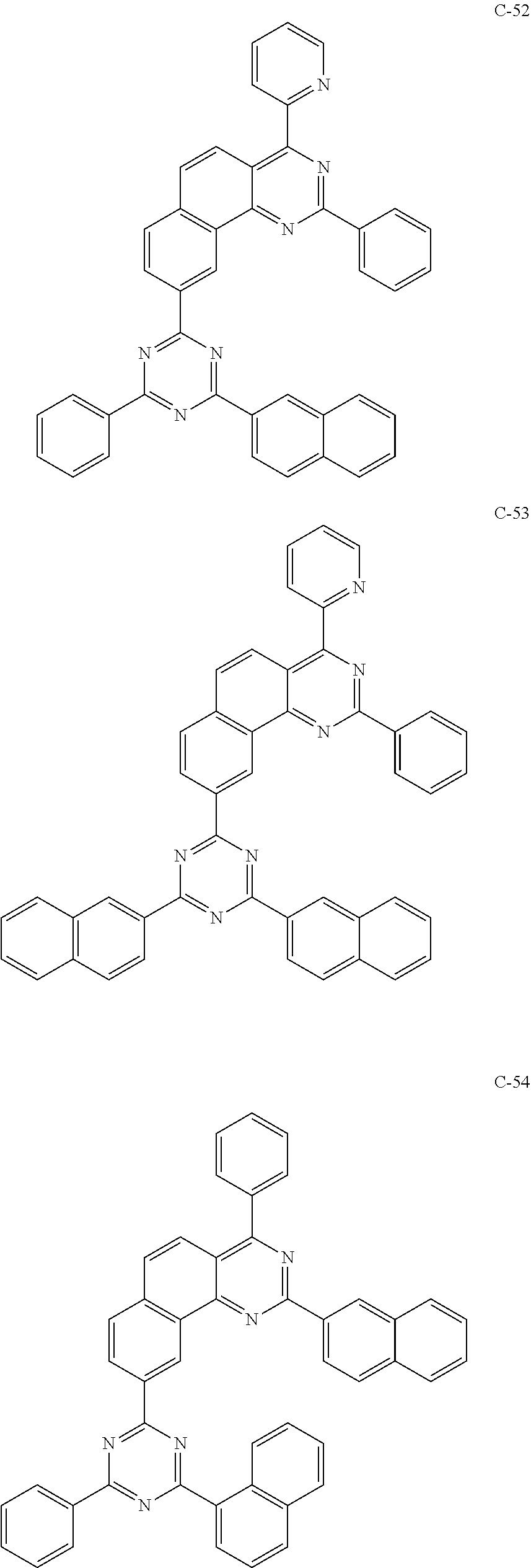


Applications Claiming Priority (3)
| Application Number | Priority Date | Filing Date | Title |
|---|---|---|---|
| KR10-2017-0050573 | 2017-04-19 | ||
| KR1020170050573A KR102372952B1 (en) | 2017-04-19 | 2017-04-19 | Organic Electroluminescent Compound and Organic Electroluminescent Device Comprising the Same |
| PCT/KR2018/004246 WO2018194314A1 (en) | 2017-04-19 | 2018-04-11 | Organic electroluminescent compound and organic electroluminescent device comprising the same |
Publications (2)
| Publication Number | Publication Date |
|---|---|
| US20200381630A1 US20200381630A1 (en) | 2020-12-03 |
| US11322692B2 true US11322692B2 (en) | 2022-05-03 |
Family
ID=63855909
Family Applications (1)
| Application Number | Title | Priority Date | Filing Date |
|---|---|---|---|
| US16/606,796 Active 2038-07-16 US11322692B2 (en) | 2017-04-19 | 2018-04-11 | Organic electroluminescent compound and organic electroluminescent device comprising the same |
Country Status (5)
| Country | Link |
|---|---|
| US (1) | US11322692B2 (en) |
| JP (1) | JP7164543B2 (en) |
| KR (1) | KR102372952B1 (en) |
| TW (1) | TW201843294A (en) |
| WO (1) | WO2018194314A1 (en) |
Families Citing this family (1)
| Publication number | Priority date | Publication date | Assignee | Title |
|---|---|---|---|---|
| CN111747933B (en) * | 2019-03-29 | 2022-03-01 | 吉林省元合电子材料有限公司 | Substituted 1,3, 5-triazine compound, composition and application thereof |
Citations (12)
| Publication number | Priority date | Publication date | Assignee | Title |
|---|---|---|---|---|
| US8318325B2 (en) | 2008-09-24 | 2012-11-27 | Lg Chem, Ltd. | Anthracene derivatives and organic electronic device using same |
| KR20140140298A (en) | 2013-05-29 | 2014-12-09 | 덕산하이메탈(주) | Compound for organic electronic element, organic electronic element using the same, and an electronic device thereof |
| KR20140141970A (en) | 2013-06-03 | 2014-12-11 | 에스에프씨 주식회사 | An organoelectro luminescent compounds and organoelectro luminescent device using the same |
| KR20150009297A (en) | 2013-07-16 | 2015-01-26 | 에스에프씨 주식회사 | An organoelectroluminescent compounds and organoelectroluminescent device using the same |
| KR20150042386A (en) | 2013-10-11 | 2015-04-21 | 에스에프씨 주식회사 | An electroluminescent compound and an electroluminescent device comprising the same |
| KR20150043571A (en) | 2013-10-11 | 2015-04-23 | 에스에프씨 주식회사 | An electroluminescent compound and an electroluminescent device comprising the same |
| KR20150080966A (en) * | 2014-01-02 | 2015-07-13 | 최돈수 | Light-emitting material for organic electroluminescent device, organic electroluminescent device using same, and material for organic electroluminescent device |
| KR20150122343A (en) | 2014-04-23 | 2015-11-02 | 덕산네오룩스 주식회사 | Compound for organic electronic element, organic electronic element using the same, and an electronic device thereof |
| KR20150124000A (en) | 2014-04-25 | 2015-11-05 | 덕산네오룩스 주식회사 | Compound for organic electronic element, organic electronic element using the same, and an electronic device thereof |
| US20160248024A1 (en) | 2013-10-11 | 2016-08-25 | Sfc Co., Ltd. | Organic light emitting compound and organic light emitting device comprising the same |
| KR20160127503A (en) | 2015-04-27 | 2016-11-04 | (주)더블유에스 | triazine derivatives and organic electroluminescent device including the same |
| US20170141329A1 (en) | 2014-06-30 | 2017-05-18 | Merck Patent Gmbh | Metal complexes |
Family Cites Families (4)
| Publication number | Priority date | Publication date | Assignee | Title |
|---|---|---|---|---|
| JP5599570B2 (en) * | 2009-02-10 | 2014-10-01 | 国立大学法人 香川大学 | Method for producing aryl derivative using heterogeneous catalyst |
| KR20140111214A (en) * | 2013-03-08 | 2014-09-18 | 에스에프씨 주식회사 | An electroluminescent compound and an electroluminescent device comprising the same |
| KR102169449B1 (en) * | 2013-10-11 | 2020-10-26 | 에스에프씨 주식회사 | An electroluminescent compound and an electroluminescent device comprising the same |
| JP7039188B2 (en) * | 2016-06-24 | 2022-03-22 | 株式会社半導体エネルギー研究所 | Host material for phosphorescent layer, organic compound, light emitting element, light emitting device, electronic device and lighting device |
-
2017
- 2017-04-19 KR KR1020170050573A patent/KR102372952B1/en active IP Right Grant
-
2018
- 2018-04-09 TW TW107112051A patent/TW201843294A/en unknown
- 2018-04-11 US US16/606,796 patent/US11322692B2/en active Active
- 2018-04-11 JP JP2019555193A patent/JP7164543B2/en active Active
- 2018-04-11 WO PCT/KR2018/004246 patent/WO2018194314A1/en active Application Filing
Patent Citations (12)
| Publication number | Priority date | Publication date | Assignee | Title |
|---|---|---|---|---|
| US8318325B2 (en) | 2008-09-24 | 2012-11-27 | Lg Chem, Ltd. | Anthracene derivatives and organic electronic device using same |
| KR20140140298A (en) | 2013-05-29 | 2014-12-09 | 덕산하이메탈(주) | Compound for organic electronic element, organic electronic element using the same, and an electronic device thereof |
| KR20140141970A (en) | 2013-06-03 | 2014-12-11 | 에스에프씨 주식회사 | An organoelectro luminescent compounds and organoelectro luminescent device using the same |
| KR20150009297A (en) | 2013-07-16 | 2015-01-26 | 에스에프씨 주식회사 | An organoelectroluminescent compounds and organoelectroluminescent device using the same |
| KR20150042386A (en) | 2013-10-11 | 2015-04-21 | 에스에프씨 주식회사 | An electroluminescent compound and an electroluminescent device comprising the same |
| KR20150043571A (en) | 2013-10-11 | 2015-04-23 | 에스에프씨 주식회사 | An electroluminescent compound and an electroluminescent device comprising the same |
| US20160248024A1 (en) | 2013-10-11 | 2016-08-25 | Sfc Co., Ltd. | Organic light emitting compound and organic light emitting device comprising the same |
| KR20150080966A (en) * | 2014-01-02 | 2015-07-13 | 최돈수 | Light-emitting material for organic electroluminescent device, organic electroluminescent device using same, and material for organic electroluminescent device |
| KR20150122343A (en) | 2014-04-23 | 2015-11-02 | 덕산네오룩스 주식회사 | Compound for organic electronic element, organic electronic element using the same, and an electronic device thereof |
| KR20150124000A (en) | 2014-04-25 | 2015-11-05 | 덕산네오룩스 주식회사 | Compound for organic electronic element, organic electronic element using the same, and an electronic device thereof |
| US20170141329A1 (en) | 2014-06-30 | 2017-05-18 | Merck Patent Gmbh | Metal complexes |
| KR20160127503A (en) | 2015-04-27 | 2016-11-04 | (주)더블유에스 | triazine derivatives and organic electroluminescent device including the same |
Also Published As
| Publication number | Publication date |
|---|---|
| JP2020517593A (en) | 2020-06-18 |
| KR20180117446A (en) | 2018-10-29 |
| JP7164543B2 (en) | 2022-11-01 |
| US20200381630A1 (en) | 2020-12-03 |
| CN110431215A (en) | 2019-11-08 |
| KR102372952B1 (en) | 2022-03-11 |
| WO2018194314A1 (en) | 2018-10-25 |
| TW201843294A (en) | 2018-12-16 |
Similar Documents
| Publication | Publication Date | Title |
|---|---|---|
| US11737353B2 (en) | Plurality of host materials and organic electroluminescent device comprising the same | |
| US10636980B2 (en) | Organic electroluminescent compound and organic electroluminescent device comprising the same | |
| US11495750B2 (en) | Organic electroluminescent compound and organic electroluminescent device comprising the same | |
| US11785846B2 (en) | Organic electroluminescent compound and organic electroluminescent device comprising the same | |
| US10547010B2 (en) | Organic electroluminescent compounds and organic electroluminescent device comprising the same | |
| US20230020540A1 (en) | Multi-component host material and organic electroluminescent device comprising the same | |
| US11450814B2 (en) | Organic electroluminescent compound and organic electroluminescent device comprising the same | |
| US20210210697A1 (en) | Multi-component host material and organic electroluminescent device comprising the same | |
| US20210257555A1 (en) | Organic electroluminescent compound and organic electroluminescent device comprising the same | |
| US20190131542A1 (en) | A plurality of host materials and organic electroluminescent device comprising the same | |
| US20170047527A1 (en) | Multi-component host material and organic electroluminescent device comprising the same | |
| US10927103B1 (en) | Organic electroluminescent compound and organic electroluminescent device comprising the same | |
| US20170256722A1 (en) | A hole transport material and an organic electroluminescent device comprising the same | |
| US20190259947A1 (en) | Organic electroluminescent device | |
| US20180190912A1 (en) | Luminescent material for delayed fluorescence and organic electroluminescent device comprising the same | |
| US20190157569A1 (en) | Organic electroluminescent compound, organic electroluminescent material and organic electroluminescent device comprising the same | |
| US20180223184A1 (en) | Organic electroluminescent compounds and organic electroluminescent device comprising the same | |
| US10797243B2 (en) | Organic electroluminescent compound and organic electroluminescent device comprising the same | |
| US10991889B2 (en) | Organic electroluminescent compound and organic electroluminescent device comprising the same | |
| US10069087B2 (en) | Organic electroluminescent compounds and organic electroluminescent device comprising the same | |
| US20190273209A1 (en) | Organic electroluminescent device | |
| US9698355B2 (en) | Organic electroluminescent compounds and organic electroluminescent device comprising the same | |
| US11289662B2 (en) | Organic electroluminescent compound and organic electroluminescent device comprising the same | |
| US10629824B2 (en) | Organic electroluminescent compound and organic electroluminescent device comprising the same | |
| US10854824B2 (en) | Organic electroluminescent compound, organic electroluminescent material and organic electroluminescent device comprising the same |
Legal Events
| Date | Code | Title | Description |
|---|---|---|---|
| FEPP | Fee payment procedure |
Free format text: ENTITY STATUS SET TO UNDISCOUNTED (ORIGINAL EVENT CODE: BIG.); ENTITY STATUS OF PATENT OWNER: LARGE ENTITY |
|
| STPP | Information on status: patent application and granting procedure in general |
Free format text: RESPONSE TO NON-FINAL OFFICE ACTION ENTERED AND FORWARDED TO EXAMINER |
|
| STPP | Information on status: patent application and granting procedure in general |
Free format text: NON FINAL ACTION MAILED |
|
| STPP | Information on status: patent application and granting procedure in general |
Free format text: AWAITING TC RESP., ISSUE FEE NOT PAID |
|
| STPP | Information on status: patent application and granting procedure in general |
Free format text: NOTICE OF ALLOWANCE MAILED -- APPLICATION RECEIVED IN OFFICE OF PUBLICATIONS |
|
| AS | Assignment |
Owner name: ROHM AND HAAS ELECTRONIC MATERIALS KOREA LTD., KOREA, REPUBLIC OF Free format text: ASSIGNMENT OF ASSIGNORS INTEREST;ASSIGNOR:MOON, DOO-HYEON;REEL/FRAME:059298/0271 Effective date: 20180308 |
|
| STPP | Information on status: patent application and granting procedure in general |
Free format text: PUBLICATIONS -- ISSUE FEE PAYMENT VERIFIED |
|
| STCF | Information on status: patent grant |
Free format text: PATENTED CASE |