US11296484B2 - Photonic generation and steering of coherent vortex beams - Google Patents
Photonic generation and steering of coherent vortex beams Download PDFInfo
- Publication number
- US11296484B2 US11296484B2 US16/614,402 US201816614402A US11296484B2 US 11296484 B2 US11296484 B2 US 11296484B2 US 201816614402 A US201816614402 A US 201816614402A US 11296484 B2 US11296484 B2 US 11296484B2
- Authority
- US
- United States
- Prior art keywords
- bic
- light
- light emitter
- holes
- emitting laser
- Prior art date
- Legal status (The legal status is an assumption and is not a legal conclusion. Google has not performed a legal analysis and makes no representation as to the accuracy of the status listed.)
- Active, expires
Links
Images


Classifications
-
- H—ELECTRICITY
- H01—ELECTRIC ELEMENTS
- H01S—DEVICES USING THE PROCESS OF LIGHT AMPLIFICATION BY STIMULATED EMISSION OF RADIATION [LASER] TO AMPLIFY OR GENERATE LIGHT; DEVICES USING STIMULATED EMISSION OF ELECTROMAGNETIC RADIATION IN WAVE RANGES OTHER THAN OPTICAL
- H01S5/00—Semiconductor lasers
- H01S5/10—Construction or shape of the optical resonator, e.g. extended or external cavity, coupled cavities, bent-guide, varying width, thickness or composition of the active region
- H01S5/18—Surface-emitting [SE] lasers, e.g. having both horizontal and vertical cavities
- H01S5/185—Surface-emitting [SE] lasers, e.g. having both horizontal and vertical cavities having only horizontal cavities, e.g. horizontal cavity surface-emitting lasers [HCSEL]
- H01S5/187—Surface-emitting [SE] lasers, e.g. having both horizontal and vertical cavities having only horizontal cavities, e.g. horizontal cavity surface-emitting lasers [HCSEL] using Bragg reflection
-
- H—ELECTRICITY
- H01—ELECTRIC ELEMENTS
- H01S—DEVICES USING THE PROCESS OF LIGHT AMPLIFICATION BY STIMULATED EMISSION OF RADIATION [LASER] TO AMPLIFY OR GENERATE LIGHT; DEVICES USING STIMULATED EMISSION OF ELECTROMAGNETIC RADIATION IN WAVE RANGES OTHER THAN OPTICAL
- H01S5/00—Semiconductor lasers
- H01S5/10—Construction or shape of the optical resonator, e.g. extended or external cavity, coupled cavities, bent-guide, varying width, thickness or composition of the active region
- H01S5/11—Comprising a photonic bandgap structure
-
- H—ELECTRICITY
- H01—ELECTRIC ELEMENTS
- H01S—DEVICES USING THE PROCESS OF LIGHT AMPLIFICATION BY STIMULATED EMISSION OF RADIATION [LASER] TO AMPLIFY OR GENERATE LIGHT; DEVICES USING STIMULATED EMISSION OF ELECTROMAGNETIC RADIATION IN WAVE RANGES OTHER THAN OPTICAL
- H01S5/00—Semiconductor lasers
- H01S5/10—Construction or shape of the optical resonator, e.g. extended or external cavity, coupled cavities, bent-guide, varying width, thickness or composition of the active region
- H01S5/18—Surface-emitting [SE] lasers, e.g. having both horizontal and vertical cavities
- H01S5/185—Surface-emitting [SE] lasers, e.g. having both horizontal and vertical cavities having only horizontal cavities, e.g. horizontal cavity surface-emitting lasers [HCSEL]
-
- H—ELECTRICITY
- H01—ELECTRIC ELEMENTS
- H01S—DEVICES USING THE PROCESS OF LIGHT AMPLIFICATION BY STIMULATED EMISSION OF RADIATION [LASER] TO AMPLIFY OR GENERATE LIGHT; DEVICES USING STIMULATED EMISSION OF ELECTROMAGNETIC RADIATION IN WAVE RANGES OTHER THAN OPTICAL
- H01S5/00—Semiconductor lasers
- H01S5/30—Structure or shape of the active region; Materials used for the active region
- H01S5/34—Structure or shape of the active region; Materials used for the active region comprising quantum well or superlattice structures, e.g. single quantum well [SQW] lasers, multiple quantum well [MQW] lasers or graded index separate confinement heterostructure [GRINSCH] lasers
- H01S5/343—Structure or shape of the active region; Materials used for the active region comprising quantum well or superlattice structures, e.g. single quantum well [SQW] lasers, multiple quantum well [MQW] lasers or graded index separate confinement heterostructure [GRINSCH] lasers in AIIIBV compounds, e.g. AlGaAs-laser, InP-based laser
-
- H—ELECTRICITY
- H01—ELECTRIC ELEMENTS
- H01S—DEVICES USING THE PROCESS OF LIGHT AMPLIFICATION BY STIMULATED EMISSION OF RADIATION [LASER] TO AMPLIFY OR GENERATE LIGHT; DEVICES USING STIMULATED EMISSION OF ELECTROMAGNETIC RADIATION IN WAVE RANGES OTHER THAN OPTICAL
- H01S2301/00—Functional characteristics
- H01S2301/20—Lasers with a special output beam profile or cross-section, e.g. non-Gaussian
- H01S2301/203—Lasers with a special output beam profile or cross-section, e.g. non-Gaussian with at least one hole in the intensity distribution, e.g. annular or doughnut mode
-
- H—ELECTRICITY
- H01—ELECTRIC ELEMENTS
- H01S—DEVICES USING THE PROCESS OF LIGHT AMPLIFICATION BY STIMULATED EMISSION OF RADIATION [LASER] TO AMPLIFY OR GENERATE LIGHT; DEVICES USING STIMULATED EMISSION OF ELECTROMAGNETIC RADIATION IN WAVE RANGES OTHER THAN OPTICAL
- H01S5/00—Semiconductor lasers
- H01S5/30—Structure or shape of the active region; Materials used for the active region
- H01S5/34—Structure or shape of the active region; Materials used for the active region comprising quantum well or superlattice structures, e.g. single quantum well [SQW] lasers, multiple quantum well [MQW] lasers or graded index separate confinement heterostructure [GRINSCH] lasers
- H01S5/343—Structure or shape of the active region; Materials used for the active region comprising quantum well or superlattice structures, e.g. single quantum well [SQW] lasers, multiple quantum well [MQW] lasers or graded index separate confinement heterostructure [GRINSCH] lasers in AIIIBV compounds, e.g. AlGaAs-laser, InP-based laser
- H01S5/3434—Structure or shape of the active region; Materials used for the active region comprising quantum well or superlattice structures, e.g. single quantum well [SQW] lasers, multiple quantum well [MQW] lasers or graded index separate confinement heterostructure [GRINSCH] lasers in AIIIBV compounds, e.g. AlGaAs-laser, InP-based laser with a well layer comprising at least both As and P as V-compounds
Definitions
- Vortices are recognized to be ubiquitous features around wave singularities, forming threads of silence in acoustic, turbulences in superfluids, and tidal waves in oceans.
- Light carrying Orbital Angular Momentum (OAM) has been intensively investigated due to interest in numerous fields including metrology, microscopy, quantum entanglement, and particle trapping.
- the theoretically unlimited orthogonal basis of OAM spatial modes makes it a candidate to overcome the data transmission capacity crunch.
- OAM in light is generally generated using non-integrated and unwieldy optical components that shape the phase front of a Gaussian laser beam. Generation methods include spiral phase plates, chiral dielectric meta-holograms, spatial light modulators, or metasurfaces.
- MEMS Micro-Electro-Mechanical Systems
- state-of-the-art optical beam steering uses mechanisms that control the phase/intensity profile of individual nanoantennas for beam forming. These mechanisms also suffer from limitations such as complexity, poor agility, and large size of non-integrated components. Furthermore, steering is usually limited to regular Gaussian beams.
- an integrated device uses wave singularities known as bound states in continuum (BIC) to simultaneously generate and steer powerful coherent beams carrying orbital angular momentum (OAM).
- BIC bound states in continuum
- OAM orbital angular momentum
- the invention may bring substantial opportunities in the manipulation of micro-particles and micro-organisms and may be useful for applications in other areas such as biological sensing, microscopy, astronomy, high-capacity communications, quantum computing, quantum data communication, LIDAR, metrology and imaging.
- BICs are singular points in the radiation region of the dispersion band diagram whose quality factor tends to infinity, which results in low threshold light sources. These singular points carry topological charges that mathematically refer to modes with singular far-field phase whose order can be identified by the far-field polarization twisting around the singular point in reciprocal or real spaces. These singular states are robust, and their position in the reciprocal space—or angle of emission in the real space—can be controlled by changing any structure parameter uniformly such as the radius of holes in photonic crystal membrane.
- An illustrative embodiment comprises a photonic crystal made of InGaAsP multiple quantum wells with periodic holes.
- InGaAsP is bonded onto a glass substrate using a PolyMethyl MethAcrylate (PMMA), which infiltrates holes.
- PMMA PolyMethyl MethAcrylate
- this structure there are three modes with large quality factors whose position in the reciprocal space (or angle in real space) can be controlled by changing the radius of holes or using electro-optic, acousto-optic, or phase-changed materials. Fabricating the structures with different radii and pumping them to achieve population inversion leads to lasing. Lasing is evidenced by the characteristic threshold behavior of the output power vs. input power plot. Also steering the emitted beam to large angles by decreasing their radius of holes is evident from reciprocal space imaging.
- the light source simultaneously generates and steers a coherent vortex beam without any additional component.
- Usually other light sources generate and steer a simple Gaussian beam using phase arrays, or only generate vortex beam and steer using bulky external components.
- the structure can be engineered to generate any arbitrary vortex beams with different singularity orders (topological charges).
- the structure is capable of generating and steering multiple beams simultaneously.
- a bound states in the continuum (BIC) surface emitting laser includes a light emitter configured to generate BIC light waves.
- the laser also includes an array of holes with equal radii extending through the light emitter such that light emitted by the light emitter upon receipt of power is emitted as a coherent vortex beam at an angle to a surface normal of the light emitter that is determined at least in part by the radius of the holes in the array.
- a method of forming a light source for generating a coherent light vortex beam is provided.
- a light emitter configured to generate BIC light waves when supplied with pump energy is provided.
- An angle is selected at which a coherent light vortex beam is to be emitted from a surface of the photonic crystal.
- a topology is selected for an array of holes to be formed in the photonic crystal based at least in part on the selected angle. The array of holes is formed so that they extend through the photonic crystal with the selected topology.
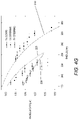
- FIG. 1A is a schematic diagram of one example of an optical light source that may be used to generate a steerable coherent vortex beam
- FIG. 1B illustrates the uniformity of the holes in the structure
- FIG. 1C shows experimental (plot) and theoretical (dots) band diagrams measured/calculated along the ⁇ X and the ⁇ M directions.
- FIGS. 2A-2F demonstrate beam steering in the high-symmetry directions of the crystal in the light source.
- FIGS. 3A-3F represent the experimental ( FIGS. 3A-3C ) and theoretical ( FIGS. 3D-3F ) far-fields of devices emitting at different angles; patterns and thus demonstrate a topological charge of +1 and ⁇ 1 for modes 3 and 1, respectively.
- FIGS. 3G-3I show self-interference patterns of the emission beams for three samples with different radii.
- FIGS. 4A-4F show the evolution of the reciprocal space image as a function of the pump power for samples of the light source supporting all three singular modes; and FIG. 4G shows the lasing wavelength as a function of the radius of holes from 180 nm to 350 nm.
- FIG. 5 is a schematic diagram illustrating one particular example of a sequence of steps for fabricating the coherent vortex beam source described herein.
- FIG. 6A shows an optical microscope image of the final light source sample fabricated in accordance with the method described in connection with FIG. 5 ;
- FIG. 6B shows a zoom-in dark field microscope image of one of arrays with a size of 200 ⁇ 200 unit cells;
- FIGS. 6 c -6 e are Scanning Electron Micrograph (SEM) images of some of the arrays with different radii: 180 nm ( FIG. 6C ), 250 nm ( FIG. 6D ), and 350 nm ( FIG. 6E ).
- SEM Scanning Electron Micrograph
- FIG. 7 shows a schematic diagram of the arrangement used to characterize the coherent vortex beam source described herein.
- FIGS. 8A-8C show the quality factor map in the 1 st Brillouin zone for modes 1 ( FIG. 8A ), 2 ( FIG. 8B ) and 3 ( FIG. 8C ).
- FIGS. 9A-9B shows the far-field pattern of the light source in which mode 1 is emitting normal to the surface and is doughnut-shaped ( FIG. 9A ), while mode 3 is emitting at an angle, and is tilted doughnut-shaped ( FIG. 9B ).
- FIGS. 10A-10C show SEM images of hole arrays with dimensions of 10 ⁇ 200 ( FIG. 10A ), 15 ⁇ 200 ( FIG. 10B ) and 25 ⁇ 200 ( FIG. 10C ).
- FIGS. 11A-11C show reciprocal space measurements for finite hole arrays with dimensions of 10 ⁇ 200 ( FIG. 11A ), 15 ⁇ 200 ( FIG. 11B ), and 25 ⁇ 200 ( FIG. 11C ).
- FIG. 12A shows the gain spectrum measurement of the unpatterned InGaAsP, bonded on a glass substrate using PMMA, as a function of pump power;
- FIG. 12B shows the calculated integrated intensity of modes 1-3 inside the volume of the gain material (InGaAsP) in a unit cell;
- FIG. 12C shows the multiplication of the gain and the intensity of the field inside the gain material to evaluate the effective gain for modes 1-3.
- FIGS. 13A-13B shows far-field measurements for arrays with radii of 250 nm ( FIG. 13A ), and 225 nm ( FIG. 13B );
- FIGS. 13C-13F show the far-field measurements when the linear polarizer in FIG. 7 is inserted in the emission path of the laser with an angle of 0°, 30°, 90° and ⁇ 45°, respectively.
- Orbital angular momentum is a fundamental degree of freedom of light that manifests itself even at the single photon level.
- the coherent generation and steering of structured light usually requires bulky and slow components.
- wave singularities known as bound states in continuum an integrated device is provided that simultaneously generates and steers powerful coherent beams carrying orbital angular momentum.
- the device brings opportunities in the manipulation of micro-particles and micro-organisms, and, may also find applications in areas such as biological sensing, microscopy, astronomy, and, high-capacity communications.
- FIG. 1A is a schematic diagram of one example of an optical light source 100 that may be used to generate a steerable coherent vortex beam 115 .
- the optical light source 100 includes an InGaAsP multiple quantum well structure 110 .
- the multiple quantum well structure 110 is tailored to emit light at telecommunication wavelengths (e.g., 1.55 microns, 1.31 microns).
- the multiple quantum well structure 110 which includes an array of holes 120 that are either devoid of material (other than air) or filled with a material that is transparent at the emitting wavelength(s) such as PolyMethyl MethAcrylate (PMMA), constitutes a Photonic Crystal (PhC).
- the PhC may be bonded on a suitable substrate such as a flat glass substrate 130 coated with a thin layer of PMMA.
- the multiple quantum well structure 110 includes two or more InGaAsP quantum well layers separated by one or more quantum well barrier layers (e.g., GaAsP, InGaAsP).
- the mole fraction of the components in each layer may be tailored so that the structure emits light at the desired wavelength(s).
- the multiple quantum well structure 110 may be initially epitaxially grown on an InP substrate.
- the holes 120 may be formed by electron beam lithography followed by dry etching.
- the resulting PhC is subsequently bonded to the flat glass substrate 130 .
- the PMMA infiltrates the holes 120 .
- the InP substrate is removed by wet etching using hydrochloric acid.
- FIG. 1(A) the light source 100 is optically pumped by an optical beam 140 and generates a vortex beam 115 at a controllable angle.
- FIG. 1(B) is a top view scanning electron micrograph of one example of the light source 100 showing the holes 120 that was fabricated to have a quantum well thickness of 300 nm, a period of 950 nm, and holes with a radius of 200 nm.
- FIG. 1B illustrates the uniformity of the holes 120 in the structure.
- FIG. 1 c shows experimental (plot) and theoretical (dots) band diagrams measured/calculated along the ⁇ X and the ⁇ M directions.
- the experimental band diagram is measured by pumping the structure with a high-energy laser and collecting the photoluminescence at different angles. A good agreement is observed between the theoretical band diagram (using finite element method) and experiments.
- FIG. 1 c presents the three modes within the gain bandwidth of InGaAsP, and, a very good agreement is observed between the theoretical and the experimental band diagrams.
- Mode 1 is a singly degenerate mode while modes 2 and 3 are doubly degenerate modes. By changing the radius of holes uniformly over the whole structure, all three modes shift spectrally.
- the quality factor of mode 1 is theoretically infinite at the center of the Brillouin zone ( ⁇ point) and independent of the radius of holes as mode 1 is symmetry protected ( ⁇ -locked).
- This type of mode (usually referred to as band-edge mode) has been extensively investigated in uniform PhC lasers that necessarily emit normal to the surface.
- Modes 2 and 3 can only have infinite quality factors if all radiation channels destructively interfere to form singular states, at reciprocal space points, known as bound states in continuum.
- FIGS. 2A-2F demonstrate beam steering in the crystal's high-symmetry directions.
- FIG. 2A shows the quality factor (Q) of modes 1-3 as a function of the radius of the holes in reciprocal space (k-space).
- the quality factors of modes 1, 2 and 3 are singular in k-space, at a point for mode 1 ( ⁇ -locked), and along lines for mode 2 (steering along ⁇ M) and mode 3 (steering along ⁇ X). Modes 2 and 3 can thus continuously steer with the radius of holes.
- the quality factor of mode 1 is singular for all radii of holes because mode 1 is symmetry-protected while mode 2 and 3 become singular for holes radii smaller than R ⁇ 250 nm.
- the dots correspond to experimental measurements, described below, of the steering angle that have been extracted from k-space imaging. The standard error in angle, from at least three measurements, is smaller than 0.5°.
- the dots are experimental measurements of the output power for different pump powers.
- the solid lines are linear fits to the data in spontaneous and stimulated emission regimes and clearly show a threshold behavior, i.e. lasing.
- the inset shows the emission power evolution as a function of the pump power in a broader wavelength range. A similar light-light curve is measured for all other lasers (not shown).
- FIG. 2C confirms normal emission from this sample.
- the steering of four lasing beams along ⁇ X is observed. They correspond mode 3, which has a large quality factor along ⁇ X, and the four beams stem from the four-fold symmetry of the crystal (invariance under 90° rotation).
- the number of beams can be controlled by the symmetry of the crystal as well as by boundary conditions.
- the steering angle further increases by decreasing the radius as seen in FIG. 2D-F .
- the emission angles are extracted from the reciprocal space images and the numerical aperture of the collecting objective.
- the dots in FIG. 2A represent the experimental emission angles, and, as can be seen, lasing occurs in directions of predicted high quality factors.
- the operating mode is selected by its spatial overlap with the optical gain and switches from mode 1 to mode 3 for R ⁇ 250 nm.
- NA numerical aperture
- the four-fold symmetry of the structure implies that any singularity is invariant under 90° rotation and this is confirmed by the four observed bright spots creating a 2-by-2 array of optical vortices (see FIG. 3 ).
- FIGS. 3 a -3 f represent the experimental ( FIGS. 3A-3C ) and theoretical ( FIGS. 3D-3F ) far-fields of devices emitting at different angles.
- mode 3 ⁇ X-steering
- R 250 nm ( FIGS. 3C and 3F )
- only mode 1 ( ⁇ -locked), emits with a doughnut-shaped far-field.
- the interference patterns comprise two inverted fork-shaped patterns and thus demonstrate a topological charge of +1 and ⁇ 1 for modes 3 and 1, respectively.
- FIGS. 3G-3I show self-interference patterns of the emission beams for three samples with different radii.
- the two inverted fork-shape patterns demonstrate a topological charge (TC) of +1 for the mode steering along ⁇ X (mode 3) and ⁇ 1 for the ⁇ -locked mode (mode 1).
- FIGS. 4A-4F present the evolution of the reciprocal space image as a function of the pump power for samples supporting all three singular modes.
- FIG. 4A clearly shows lasing along ⁇ X.
- mode 2 the threshold of the mode steering along ⁇ M
- FIGS. 4C and 4F the emission power of the lasing modes, making them brighter.
- additional spots appear (at a smaller angle) as the pump power is increased ( FIGS. 4D-4F ).
- the threshold of the mode steering along ⁇ M (mode 2, threshold ⁇ M ) is larger than the threshold of the mode steering along ⁇ X (mode 3, threshold ⁇ X ).
- the mode steering along ⁇ X is the only mode lasing in the device.
- FIG. 4G shows the lasing wavelength as a function of the radius of holes from 180 nm to 350 nm.
- the continuous lines represent the theoretical prediction of the wavelength of each mode with large quality factor as a function of the radius of holes.
- Dots represent measured wavelengths of emissions from the lasers. Each point corresponds to a device with a specific radius. Error bars indicate the standard deviation of radii measured from fabricated devices.
- Solid lines represent the wavelength of the singularities (resonances with large quality factor) of mode 1 (line 210 ), mode 2 (line 220 ), and mode 3 (line 230 ) for different radii of the holes. The good agreement between theory and experiment constitutes an additional identification of the modes.
- FIG. 5 is a schematic diagram illustrating one particular example of a sequence of steps for fabricating the coherent vortex beam source described herein.
- the formation of the multiple quantum well wafer 200 is shown in steps 1-4.
- the active layer of the wafer 200 includes an InGaAsP multiple quantum well structure 210 , the layers of which are epitaxially grown on a lattice-matched InP substrate 215 (step 1).
- the InGaAsP multiple quantum well structure 210 may be a prefabricated, commercially available structure.
- the thickness of the InGaAsP is finely controlled to be 300 nm.
- a 10 nm InP protective layer 220 is formed on top of InGaAsP.
- the top InP protective layer 220 is removed by dipping the sample in a chemical solution of HCl:H 2 O (3:1) for 60 sec (step 2).
- a Hydrogen SilsesQuioxane (HSQ) negative tone resist 225 is then coated onto the InGaAsP multiple quantum well structure 210 before electron beam lithography (step 3).
- the written pattern is transferred onto InGaAsP using a dry etch process (e.g., reactive ion etching) using H 2 :CH 4 :Ar (40:10:7) for seven minutes.
- the HSQ resist 225 is then removed by dipping it into the hydrofluoric acid (step 4) to complete the patterning of the multiple quantum well wafer 200 .
- a layer 235 of PolyMethyl MethAcrylate (PMMA) A9 is applied to a glass substrate 230 to bond the sample onto the glass substrate 230 (step 5).
- PMMA PolyMethyl MethAcrylate
- step 5 a layer 235 of PolyMethyl MethAcrylate (PMMA) A9 is applied to a glass substrate 230 to bond the sample onto the glass substrate 230 (step 5).
- PMMA is coated onto glass for 60 sec with a spinning speed and acceleration of 4000 rpm and 1000 rpm/sec, respectively.
- the sample is then annealed at 185° C. for five minutes, completing the formation of the PMMA layer 235 on the glass substrate 230 .
- the multiple quantum well wafer 200 is subsequently bonded on the glass substrate 230 by positioning the InGaAsP multiple quantum well structure 210 on the PMMA layer 235 . Bonding is accomplished with a clamp to apply uniform pressure.
- the entire structure is then put into an oven for curing at 240° C. for one hour under 40 kPa pressure.
- the curing process lasts for about five hours in total, including about one hour to raise the temperature from room temperature to 240° C., one hour of curing at this temperature and about three hours to cool down the sample to room temperature (step 6). Due to the high pressure and temperature, the PMMA infiltrates the holes that were etched in the multiple quantum well structure 210 .
- the InP substrate 215 is removed using a chemical solution of HCl:H 2 O (3:1) (step 7).
- This solution does not etch the glass, the PMMA or the InGaAsP.
- the whole etching process to remove the InP lasts about one hour.
- This step is also visually controllable, because InGaAsP is perfectly crystalline and is thus flat and visually reflective, whereas InP becomes rough during etching.
- etching stops stops.
- the resulting structure is then removed from the solution and rinsed with deionized (DI) water.
- DI deionized
- FIG. 6 a shows an optical microscope image of the final sample fabricated in accordance with the method described in connection with FIG. 5 .
- the sample contains different 200 ⁇ 200 arrays with the radii between 180-350 nm.
- FIGS. 6C-6E are Scanning Electron Micrograph (SEM) images of some of the arrays with different radii: 180 nm ( FIG. 6C ), 250 nm ( FIG. 6D ), and 350 nm ( FIG. 6E ).
- FIG. 7 shows a schematic diagram of the arrangement used to characterize the coherent vortex beam source described above.
- a high-energy laser source generates a pump beam at a wavelength of 1064 nm to induce population inversion in the InGaAsP structure.
- the power of the pump laser illuminating the sample is finely controlled.
- the spot width of the pump laser which initially is 3 mm 2 , is reduced and collimated using two lenses (lenses 1 and 2) before reaching the objective lens.
- An objective lens with a numerical aperture and magnification of 0.4 and X20 is used to pump the sample and collect the emission simultaneously.
- the emitted power from the sample which is in the wavelength range of 1400-1700 nm, is directed to the spectrum analyzer configured as a monochromator (CVI Digikrom DK480) in conjunction with a cooled InGaAs detector in lock-in detection configuration.
- the spectrum analyzer configured as a monochromator (CVI Digikrom DK480) in conjunction with a cooled InGaAs detector in lock-in detection configuration.
- the light can be directed to an infrared camera for real space or reciprocal space imaging by placing the camera in the real plane or Fourier plane, respectively.
- the configuration shown in the inset of FIG. 7 is placed in the emission path.
- the configuration includes two beam splitters and two mirrors mounted on a translation stage, enabling a fine control of the optical path difference between the two interfering beams.
- FIGS. 8 a -8 c show the quality factor map in the 1 st Brillouin zone for modes 1 ( FIG. 8A ), 2 ( FIG. 8B ) and 3 ( FIG. 8C ).
- Mode 1 has a large quality factor at the center of the 1 st Brillouin zone ( ⁇ point), while modes 2 and 3 have large quality factors along ⁇ M and ⁇ X directions, respectively).
- a unit cell was used with periodic boundary conditions in the x-y plane, and Perfectly Matched Layers (PML) in the normal direction.
- the substrate is glass with a refractive index of 1.5, while the cladding is air.
- PMMA used for bonding the InGaAsP onto glass has a refractive index of 1.5.
- FIGS. 9A-9B shows the far-field pattern of the light source in which mode 1 is emitting normal to the surface and is doughnut-shaped ( FIG. 9A ), while mode 3 is emitting at an angle, and is tilted doughnut-shaped ( FIG. 9B ).
- the fabricated arrays are quite large arrays with dimensions of 200 ⁇ 200 unit cells.
- the four-fold symmetry i.e., invariance under 90° rotation implies that any singular state in reciprocal space must have the same symmetry. Consequently, four beams in the emission should be observed ( FIGS. 2C-2F ).
- the in-plane feedback between the Floquet-Bloch waves in certain directions we can actually control the number of beams. For instance, by choosing crystals with different symmetries/dimensionalities, e.g., 1D crystal, which is invariant under 180° rotation (two-fold symmetry), two beams instead of four beams should be observed.
- Another possible method, which was used here, is to control the in-plane feedback by bringing certain boundaries closer.
- Several arrays were fabricated with different sizes of unit cells in x and y directions, 10 ⁇ 200, 15 ⁇ 200, and 25 ⁇ 200.
- the in-plane feedback along the short direction is drastically reduced, almost suppressed, while it remains the same in the long direction.
- FIGS. 10A-10C show SEM images of hole arrays with dimensions of 10 ⁇ 200 ( FIG. 10A ), 15 ⁇ 200 ( FIG. 10B ) and 25 ⁇ 200 ( FIG. 10C ).
- NA numerical aperture
- Arrays of 25 ⁇ 200 are large enough to induce sufficient in-plane feedback along both directions of periodicity to enable lasing.
- the two beams along the vertical axis are brighter than the other two along the horizontal axis.
- FIG. 12A shows the gain spectrum measurement of the unpatterned InGaAsP, bonded on a glass substrate using PMMA, as a function of pump power.
- FIG. 12B shows the calculated integrated intensity of modes 1-3 inside the volume of the gain material (InGaAsP) in a unit cell.
- FIG. 12C shows the multiplication of the gain and the intensity of the field inside the gain material to evaluate the effective gain for modes 1-3. Mode 3 has larger effective gain than the other modes in a radius range of 170-200 nm, where all three modes have large quality factors.
- mode 1 is the only one with a large quality factor.
- modes 2 and 3 also have large quality factors and gain competition then takes place.
- mode 3 experiences more gain because it has a shorter wavelength compared to the other two modes, and mode 1 experiences less gain because it has a longer wavelength ( FIG. 12A ).
- the field intensity confinement inside the gain material for mode 3 is larger than mode 1 and 2 ( FIG. 12B ), which ultimately results in larger effective gain for mode 3 ( FIG. 12C ). Therefore, mode 3 lases with a smaller threshold power compared to the other modes.
- mode 2 also starts lasing as shown in FIG. 4 .
- the threshold power of mode 1 is comparable to the damage threshold of the gain material for small radii.
- FIGS. 13A-13B shows far-field measurements for arrays with radii of 250 nm ( FIG. 13A ), and 225 nm ( FIG. 13B ).
- the movable mirror shown in FIG. 7
- the measured far-field patterns agree with the simulations shown in FIG. 9 .
- a linear polarizer in the path of the emission beam, a two-lobed intensity pattern is observed, which rotates by rotating the polarizer. Similar results were obtained for all arrays with different radii, further confirming the doughnut-shaped far-field patterns.
- FIGS. 13A-13B shows far-field measurements for arrays with radii of 250 nm ( FIG. 13A ), and 225 nm ( FIG. 13B ).
- 13C-13F show the far-field measurements when the linear polarizer is inserted in the emission path of the laser with an angle of 0°, 30°, 90° and ⁇ 45°, respectively. These results lead to the observation of two-lobe shaped patterns coming from doughnut-shaped mode.
- the arrows in the inset show the direction of the polarizer.
- a topological light source has been demonstrated that generates and steers coherent vortex beams from a fully integrated laser.
- the device made of an array of holes in InGaAsP multiple quantum wells, operates at singular points where destructive interference occurs between radiative channels of the photonic structure. These points continuously move along lines in reciprocal space as a function of the radius of holes.
- the integrated system emits light with orbital angular momentum that can be steered in arbitrary directions controlled by the symmetry of the crystal without requiring mechanical components or breaking the in-plane symmetry of the system for beam forming.
- Dynamical beam steering could be implemented by bonding the structure on electro-optic, acousto-optic, or phase-changed materials.
- the proposed scalable and steerable vortex beam source open unprecedented opportunities in micro-particles and micro-organisms manipulation as it enables not only their remote trapping and rotation from powerful emitted beams but also their translation.
- the device will find applications in multiple areas such as biological sensing, microscopy, astronomy, and high-capacity communications, for example.
- While the techniques described herein have been described in terms of a multiple quantum well structure that is formed from a material system comprising InGaAs grown over InP, these techniques may be equally applied to multiple quantum well structures formed from other material systems including, for instance, InAlGaAs/InGaAs and AlGaSb/GaSb. These material systems may result in light sources that operate any suitable wavelengths(s), including wavelengths in the ultraviolet and visible spectral bands. Moreover, these techniques may also be applied to semiconductor light emitters other than multiple quantum well structures. For instance, the present techniques may be applied to bulk semiconductor light emitting materials.
Landscapes
- Physics & Mathematics (AREA)
- Condensed Matter Physics & Semiconductors (AREA)
- General Physics & Mathematics (AREA)
- Electromagnetism (AREA)
- Optics & Photonics (AREA)
- Optical Modulation, Optical Deflection, Nonlinear Optics, Optical Demodulation, Optical Logic Elements (AREA)
Abstract
Description
where ϕ(k)=arg [cx(k)+icy(k)], and cx/cy are x/y components of the averaged field, <uk>, and uk is defined as the periodic part of the Floquet-Bloch modes, E(r, k)=eik.ruk(r). Following this procedure, topological charges of −1, −1, and +1 were obtained for
Claims (21)
Priority Applications (1)
| Application Number | Priority Date | Filing Date | Title |
|---|---|---|---|
| US16/614,402 US11296484B2 (en) | 2017-05-16 | 2018-05-16 | Photonic generation and steering of coherent vortex beams |
Applications Claiming Priority (3)
| Application Number | Priority Date | Filing Date | Title |
|---|---|---|---|
| US201762506765P | 2017-05-16 | 2017-05-16 | |
| PCT/US2018/032913 WO2018213410A1 (en) | 2017-05-16 | 2018-05-16 | Photonic generation and steering of coherent vortex beams |
| US16/614,402 US11296484B2 (en) | 2017-05-16 | 2018-05-16 | Photonic generation and steering of coherent vortex beams |
Publications (2)
| Publication Number | Publication Date |
|---|---|
| US20200203926A1 US20200203926A1 (en) | 2020-06-25 |
| US11296484B2 true US11296484B2 (en) | 2022-04-05 |
Family
ID=64274789
Family Applications (1)
| Application Number | Title | Priority Date | Filing Date |
|---|---|---|---|
| US16/614,402 Active 2038-08-12 US11296484B2 (en) | 2017-05-16 | 2018-05-16 | Photonic generation and steering of coherent vortex beams |
Country Status (2)
| Country | Link |
|---|---|
| US (1) | US11296484B2 (en) |
| WO (1) | WO2018213410A1 (en) |
Families Citing this family (13)
| Publication number | Priority date | Publication date | Assignee | Title |
|---|---|---|---|---|
| US11531111B2 (en) * | 2019-05-21 | 2022-12-20 | Northrop Grumman Systems Corporation | 360 degrees field of view scanning lidar with no movable parts |
| US11555891B2 (en) * | 2019-05-21 | 2023-01-17 | Northrop Grumman Systems Corporation | Methods for large angle field of view scanning LIDAR with no movable parts |
| DE112020003295T5 (en) * | 2019-07-11 | 2022-04-07 | Kyoto University | THREE-DIMENSIONAL DETECTION SYSTEM |
| JP7510641B2 (en) | 2019-07-11 | 2024-07-04 | ローム株式会社 | 3D Sensing System |
| CN111370994B (en) * | 2020-03-18 | 2020-12-22 | 长春理工大学 | Vertical cavity surface emitting semiconductor laser with upper electrode and middle electrode pair distributed in angle |
| US11921136B2 (en) | 2020-08-20 | 2024-03-05 | The Regents Of The University Of California | Exceptional points of degeneracy in linear time periodic systems and exceptional sensitivity |
| CN112117632B (en) * | 2020-09-21 | 2021-09-24 | 中国人民解放军国防科技大学 | Vortex light generation system and method based on liquid crystal array |
| CN112751197B (en) * | 2020-12-25 | 2021-11-09 | 电子科技大学 | Phase-control vortex electromagnetic wave generation system and method |
| US20240128717A1 (en) * | 2021-02-25 | 2024-04-18 | Kyoto University | Two-dimensional photonic crystal laser |
| JP2023131321A (en) * | 2022-03-09 | 2023-09-22 | 浜松ホトニクス株式会社 | Phase distribution design method, phase distribution design device, phase distribution design program, and recording medium |
| JP2023131320A (en) * | 2022-03-09 | 2023-09-22 | 浜松ホトニクス株式会社 | Semiconductor light emitting element |
| JP2023156941A (en) * | 2022-04-13 | 2023-10-25 | 国立大学法人京都大学 | light emitting device |
| CN116500583B (en) * | 2023-03-24 | 2024-04-16 | 扬州群发换热器有限公司 | Laser scanning control system based on optical phased array |
Citations (8)
| Publication number | Priority date | Publication date | Assignee | Title |
|---|---|---|---|---|
| US6468823B1 (en) * | 1999-09-30 | 2002-10-22 | California Institute Of Technology | Fabrication of optical devices based on two dimensional photonic crystal structures and apparatus made thereby |
| US20040089866A1 (en) * | 2002-11-01 | 2004-05-13 | Yasuaki Nagashima | Semiconductor light emitting device in which high-power light output can be obtained with a simple structure |
| US20100171130A1 (en) | 2008-12-17 | 2010-07-08 | Qinetiq Limited | Semiconductor device and fabrication method |
| US20100321478A1 (en) | 2004-01-13 | 2010-12-23 | Ip Foundry Inc. | Microdroplet-based 3-D volumetric displays utilizing emitted and moving droplet projection screens |
| US20120072931A1 (en) | 2009-06-05 | 2012-03-22 | Masahiro Imada | Surface emitting semiconductor laser, optical recording head, and optical recording apparatus |
| EP3035456A1 (en) | 2014-12-15 | 2016-06-22 | Université Montpellier 2 Sciences et Techniques | Laser device with a beam carrying controlled orbital angular momentum. |
| US20170077667A1 (en) | 2015-09-14 | 2017-03-16 | The Regents Of The University Of California | Quantum cascade external cavity laser with metasurfaces |
| WO2017066095A1 (en) | 2015-10-13 | 2017-04-20 | The Regents Of The University Of California | System and method for bound state in continuum laser sources |
-
2018
- 2018-05-16 WO PCT/US2018/032913 patent/WO2018213410A1/en active Application Filing
- 2018-05-16 US US16/614,402 patent/US11296484B2/en active Active
Patent Citations (8)
| Publication number | Priority date | Publication date | Assignee | Title |
|---|---|---|---|---|
| US6468823B1 (en) * | 1999-09-30 | 2002-10-22 | California Institute Of Technology | Fabrication of optical devices based on two dimensional photonic crystal structures and apparatus made thereby |
| US20040089866A1 (en) * | 2002-11-01 | 2004-05-13 | Yasuaki Nagashima | Semiconductor light emitting device in which high-power light output can be obtained with a simple structure |
| US20100321478A1 (en) | 2004-01-13 | 2010-12-23 | Ip Foundry Inc. | Microdroplet-based 3-D volumetric displays utilizing emitted and moving droplet projection screens |
| US20100171130A1 (en) | 2008-12-17 | 2010-07-08 | Qinetiq Limited | Semiconductor device and fabrication method |
| US20120072931A1 (en) | 2009-06-05 | 2012-03-22 | Masahiro Imada | Surface emitting semiconductor laser, optical recording head, and optical recording apparatus |
| EP3035456A1 (en) | 2014-12-15 | 2016-06-22 | Université Montpellier 2 Sciences et Techniques | Laser device with a beam carrying controlled orbital angular momentum. |
| US20170077667A1 (en) | 2015-09-14 | 2017-03-16 | The Regents Of The University Of California | Quantum cascade external cavity laser with metasurfaces |
| WO2017066095A1 (en) | 2015-10-13 | 2017-04-20 | The Regents Of The University Of California | System and method for bound state in continuum laser sources |
Non-Patent Citations (1)
| Title |
|---|
| Lepetit et al. ("Resonantly Trapped Bound State in the Continuum Laser," Aug. 21, 2015 <URL:https://arxiv.org/ftp/arxiv/papers/1508/1508.05164.pdf>) (Year: 2015). * |
Also Published As
| Publication number | Publication date |
|---|---|
| US20200203926A1 (en) | 2020-06-25 |
| WO2018213410A1 (en) | 2018-11-22 |
Similar Documents
| Publication | Publication Date | Title |
|---|---|---|
| US11296484B2 (en) | Photonic generation and steering of coherent vortex beams | |
| US11391866B2 (en) | High quality factor non-uniform metasurfaces | |
| EP3035456B1 (en) | Laser device with a beam carrying controlled orbital angular momentum. | |
| US10054839B1 (en) | Nonlinear optical frequency conversion using metamaterial arrays | |
| Bahari et al. | Integrated and steerable vortex lasers using bound states in continuum | |
| JP6816037B2 (en) | How to tune one or more resonators | |
| US20210103163A1 (en) | Optomechanical modulator | |
| WO2016066998A1 (en) | Methods and devices incorporating surface nanoscale axial photonics | |
| US11152768B2 (en) | System and method for bound state in continuum laser sources | |
| Chen et al. | Ultra-compact beam steering nanolasers | |
| Bahari | Topological Photonics Light Sources | |
| US20240168358A1 (en) | High Quality Factor Metasurfaces for Wavefront Manipulation | |
| Jiang et al. | Coherent Perfect Absorption in Chaotic Optical Microresonators for Efficient Modal Control | |
| O'Brien et al. | Photonic crystal microcavity lasers | |
| Tripathi et al. | Active and lasing dielectric metasurfaces | |
| Wang et al. | Active beam steering enabled by photonic crystal surface emitting laser | |
| Zhong et al. | Ultralow-threshold Continuous-wave Quantum Dot Lasers Based on Minituarized Bound States in the Continuum | |
| Buyukkaya | Integration of Classical/Nonclassical Optical Nonlinearities With Photonic Circuits | |
| Wu | Nonlinearity of exciton polaritons in perovskite microcavities | |
| Maldaner | Towards a monolithic process for open-access Fabry-Perot etalon cavities | |
| Hueros | BACHELOR OF SCIENCE in PHYSICS | |
| Leclercq et al. | Surface operating photonic devices based on 2D photonic crystal: toward 2.5 dimensional microphotonics | |
| Lim | Design and fabrication of one-dimensional and two-dimensional photonic bandgap devices | |
| Dong et al. | Compact low loss silicon-on-insulator waveguide for broadband mid-infrared photonics | |
| Pennington et al. | Mode structure and tunability of adaptive, hemispherical microcavities |
Legal Events
| Date | Code | Title | Description |
|---|---|---|---|
| FEPP | Fee payment procedure |
Free format text: ENTITY STATUS SET TO UNDISCOUNTED (ORIGINAL EVENT CODE: BIG.); ENTITY STATUS OF PATENT OWNER: SMALL ENTITY |
|
| FEPP | Fee payment procedure |
Free format text: ENTITY STATUS SET TO SMALL (ORIGINAL EVENT CODE: SMAL); ENTITY STATUS OF PATENT OWNER: SMALL ENTITY |
|
| STPP | Information on status: patent application and granting procedure in general |
Free format text: DOCKETED NEW CASE - READY FOR EXAMINATION |
|
| AS | Assignment |
Owner name: THE REGENTS OF THE UNIVERSITY OF CALIFORNIA, CALIFORNIA Free format text: ASSIGNMENT OF ASSIGNORS INTEREST;ASSIGNORS:KANTE, BOUBACAR;BAHARI, BABAK;REEL/FRAME:054704/0399 Effective date: 20170516 |
|
| STPP | Information on status: patent application and granting procedure in general |
Free format text: NON FINAL ACTION MAILED |
|
| STPP | Information on status: patent application and granting procedure in general |
Free format text: RESPONSE TO NON-FINAL OFFICE ACTION ENTERED AND FORWARDED TO EXAMINER |
|
| STPP | Information on status: patent application and granting procedure in general |
Free format text: NOTICE OF ALLOWANCE MAILED -- APPLICATION RECEIVED IN OFFICE OF PUBLICATIONS |
|
| STPP | Information on status: patent application and granting procedure in general |
Free format text: PUBLICATIONS -- ISSUE FEE PAYMENT VERIFIED |
|
| STCF | Information on status: patent grant |
Free format text: PATENTED CASE |