US11296144B2 - Image display device - Google Patents
Image display device Download PDFInfo
- Publication number
- US11296144B2 US11296144B2 US16/929,817 US202016929817A US11296144B2 US 11296144 B2 US11296144 B2 US 11296144B2 US 202016929817 A US202016929817 A US 202016929817A US 11296144 B2 US11296144 B2 US 11296144B2
- Authority
- US
- United States
- Prior art keywords
- electrode
- light emission
- external coupling
- micro light
- layer
- Prior art date
- Legal status (The legal status is an assumption and is not a legal conclusion. Google has not performed a legal analysis and makes no representation as to the accuracy of the status listed.)
- Active
Links
Images


Classifications
-
- H—ELECTRICITY
- H10—SEMICONDUCTOR DEVICES; ELECTRIC SOLID-STATE DEVICES NOT OTHERWISE PROVIDED FOR
- H10H—INORGANIC LIGHT-EMITTING SEMICONDUCTOR DEVICES HAVING POTENTIAL BARRIERS
- H10H29/00—Integrated devices, or assemblies of multiple devices, comprising at least one light-emitting semiconductor element covered by group H10H20/00
- H10H29/10—Integrated devices comprising at least one light-emitting semiconductor component covered by group H10H20/00
- H10H29/14—Integrated devices comprising at least one light-emitting semiconductor component covered by group H10H20/00 comprising multiple light-emitting semiconductor components
- H10H29/142—Two-dimensional arrangements, e.g. asymmetric LED layout
-
- H01L27/156—
-
- H—ELECTRICITY
- H01—ELECTRIC ELEMENTS
- H01L—SEMICONDUCTOR DEVICES NOT COVERED BY CLASS H10
- H01L25/00—Assemblies consisting of a plurality of semiconductor or other solid state devices
- H01L25/18—Assemblies consisting of a plurality of semiconductor or other solid state devices the devices being of the types provided for in two or more different main groups of the same subclass of H10B, H10D, H10F, H10H, H10K or H10N
-
- H—ELECTRICITY
- H01—ELECTRIC ELEMENTS
- H01L—SEMICONDUCTOR DEVICES NOT COVERED BY CLASS H10
- H01L25/00—Assemblies consisting of a plurality of semiconductor or other solid state devices
- H01L25/50—Multistep manufacturing processes of assemblies consisting of devices, the devices being individual devices of subclass H10D or integrated devices of class H10
-
- H01L33/24—
-
- H01L33/38—
-
- H01L33/405—
-
- H01L33/44—
-
- H01L33/62—
-
- H—ELECTRICITY
- H01—ELECTRIC ELEMENTS
- H01S—DEVICES USING THE PROCESS OF LIGHT AMPLIFICATION BY STIMULATED EMISSION OF RADIATION [LASER] TO AMPLIFY OR GENERATE LIGHT; DEVICES USING STIMULATED EMISSION OF ELECTROMAGNETIC RADIATION IN WAVE RANGES OTHER THAN OPTICAL
- H01S5/00—Semiconductor lasers
- H01S5/02—Structural details or components not essential to laser action
- H01S5/0206—Substrates, e.g. growth, shape, material, removal or bonding
- H01S5/0215—Bonding to the substrate
- H01S5/0216—Bonding to the substrate using an intermediate compound, e.g. a glue or solder
-
- H—ELECTRICITY
- H01—ELECTRIC ELEMENTS
- H01S—DEVICES USING THE PROCESS OF LIGHT AMPLIFICATION BY STIMULATED EMISSION OF RADIATION [LASER] TO AMPLIFY OR GENERATE LIGHT; DEVICES USING STIMULATED EMISSION OF ELECTROMAGNETIC RADIATION IN WAVE RANGES OTHER THAN OPTICAL
- H01S5/00—Semiconductor lasers
- H01S5/02—Structural details or components not essential to laser action
- H01S5/022—Mountings; Housings
- H01S5/023—Mount members, e.g. sub-mount members
- H01S5/02325—Mechanically integrated components on mount members or optical micro-benches
-
- H—ELECTRICITY
- H01—ELECTRIC ELEMENTS
- H01S—DEVICES USING THE PROCESS OF LIGHT AMPLIFICATION BY STIMULATED EMISSION OF RADIATION [LASER] TO AMPLIFY OR GENERATE LIGHT; DEVICES USING STIMULATED EMISSION OF ELECTROMAGNETIC RADIATION IN WAVE RANGES OTHER THAN OPTICAL
- H01S5/00—Semiconductor lasers
- H01S5/02—Structural details or components not essential to laser action
- H01S5/028—Coatings ; Treatment of the laser facets, e.g. etching, passivation layers or reflecting layers
-
- H—ELECTRICITY
- H01—ELECTRIC ELEMENTS
- H01S—DEVICES USING THE PROCESS OF LIGHT AMPLIFICATION BY STIMULATED EMISSION OF RADIATION [LASER] TO AMPLIFY OR GENERATE LIGHT; DEVICES USING STIMULATED EMISSION OF ELECTROMAGNETIC RADIATION IN WAVE RANGES OTHER THAN OPTICAL
- H01S5/00—Semiconductor lasers
- H01S5/04—Processes or apparatus for excitation, e.g. pumping, e.g. by electron beams
- H01S5/042—Electrical excitation ; Circuits therefor
- H01S5/0425—Electrodes, e.g. characterised by the structure
- H01S5/04256—Electrodes, e.g. characterised by the structure characterised by the configuration
- H01S5/04257—Electrodes, e.g. characterised by the structure characterised by the configuration having positive and negative electrodes on the same side of the substrate
-
- H—ELECTRICITY
- H01—ELECTRIC ELEMENTS
- H01S—DEVICES USING THE PROCESS OF LIGHT AMPLIFICATION BY STIMULATED EMISSION OF RADIATION [LASER] TO AMPLIFY OR GENERATE LIGHT; DEVICES USING STIMULATED EMISSION OF ELECTROMAGNETIC RADIATION IN WAVE RANGES OTHER THAN OPTICAL
- H01S5/00—Semiconductor lasers
- H01S5/10—Construction or shape of the optical resonator, e.g. extended or external cavity, coupled cavities, bent-guide, varying width, thickness or composition of the active region
- H01S5/18—Surface-emitting [SE] lasers, e.g. having both horizontal and vertical cavities
- H01S5/183—Surface-emitting [SE] lasers, e.g. having both horizontal and vertical cavities having only vertical cavities, e.g. vertical cavity surface-emitting lasers [VCSEL]
- H01S5/18344—Surface-emitting [SE] lasers, e.g. having both horizontal and vertical cavities having only vertical cavities, e.g. vertical cavity surface-emitting lasers [VCSEL] characterized by the mesa, e.g. dimensions or shape of the mesa
- H01S5/18347—Mesa comprising active layer
-
- H—ELECTRICITY
- H01—ELECTRIC ELEMENTS
- H01S—DEVICES USING THE PROCESS OF LIGHT AMPLIFICATION BY STIMULATED EMISSION OF RADIATION [LASER] TO AMPLIFY OR GENERATE LIGHT; DEVICES USING STIMULATED EMISSION OF ELECTROMAGNETIC RADIATION IN WAVE RANGES OTHER THAN OPTICAL
- H01S5/00—Semiconductor lasers
- H01S5/10—Construction or shape of the optical resonator, e.g. extended or external cavity, coupled cavities, bent-guide, varying width, thickness or composition of the active region
- H01S5/18—Surface-emitting [SE] lasers, e.g. having both horizontal and vertical cavities
- H01S5/183—Surface-emitting [SE] lasers, e.g. having both horizontal and vertical cavities having only vertical cavities, e.g. vertical cavity surface-emitting lasers [VCSEL]
- H01S5/18361—Structure of the reflectors, e.g. hybrid mirrors
- H01S5/18375—Structure of the reflectors, e.g. hybrid mirrors based on metal reflectors
-
- H—ELECTRICITY
- H10—SEMICONDUCTOR DEVICES; ELECTRIC SOLID-STATE DEVICES NOT OTHERWISE PROVIDED FOR
- H10H—INORGANIC LIGHT-EMITTING SEMICONDUCTOR DEVICES HAVING POTENTIAL BARRIERS
- H10H20/00—Individual inorganic light-emitting semiconductor devices having potential barriers, e.g. light-emitting diodes [LED]
- H10H20/01—Manufacture or treatment
- H10H20/011—Manufacture or treatment of bodies, e.g. forming semiconductor layers
- H10H20/013—Manufacture or treatment of bodies, e.g. forming semiconductor layers having light-emitting regions comprising only Group III-V materials
- H10H20/0137—Manufacture or treatment of bodies, e.g. forming semiconductor layers having light-emitting regions comprising only Group III-V materials the light-emitting regions comprising nitride materials
-
- H—ELECTRICITY
- H10—SEMICONDUCTOR DEVICES; ELECTRIC SOLID-STATE DEVICES NOT OTHERWISE PROVIDED FOR
- H10H—INORGANIC LIGHT-EMITTING SEMICONDUCTOR DEVICES HAVING POTENTIAL BARRIERS
- H10H20/00—Individual inorganic light-emitting semiconductor devices having potential barriers, e.g. light-emitting diodes [LED]
- H10H20/80—Constructional details
- H10H20/81—Bodies
- H10H20/819—Bodies characterised by their shape, e.g. curved or truncated substrates
- H10H20/821—Bodies characterised by their shape, e.g. curved or truncated substrates of the light-emitting regions, e.g. non-planar junctions
-
- H—ELECTRICITY
- H10—SEMICONDUCTOR DEVICES; ELECTRIC SOLID-STATE DEVICES NOT OTHERWISE PROVIDED FOR
- H10H—INORGANIC LIGHT-EMITTING SEMICONDUCTOR DEVICES HAVING POTENTIAL BARRIERS
- H10H20/00—Individual inorganic light-emitting semiconductor devices having potential barriers, e.g. light-emitting diodes [LED]
- H10H20/80—Constructional details
- H10H20/83—Electrodes
- H10H20/831—Electrodes characterised by their shape
- H10H20/8312—Electrodes characterised by their shape extending at least partially through the bodies
-
- H—ELECTRICITY
- H10—SEMICONDUCTOR DEVICES; ELECTRIC SOLID-STATE DEVICES NOT OTHERWISE PROVIDED FOR
- H10H—INORGANIC LIGHT-EMITTING SEMICONDUCTOR DEVICES HAVING POTENTIAL BARRIERS
- H10H20/00—Individual inorganic light-emitting semiconductor devices having potential barriers, e.g. light-emitting diodes [LED]
- H10H20/80—Constructional details
- H10H20/83—Electrodes
- H10H20/831—Electrodes characterised by their shape
- H10H20/8314—Electrodes characterised by their shape extending at least partially onto an outer side surface of the bodies
-
- H—ELECTRICITY
- H10—SEMICONDUCTOR DEVICES; ELECTRIC SOLID-STATE DEVICES NOT OTHERWISE PROVIDED FOR
- H10H—INORGANIC LIGHT-EMITTING SEMICONDUCTOR DEVICES HAVING POTENTIAL BARRIERS
- H10H20/00—Individual inorganic light-emitting semiconductor devices having potential barriers, e.g. light-emitting diodes [LED]
- H10H20/80—Constructional details
- H10H20/83—Electrodes
- H10H20/832—Electrodes characterised by their material
- H10H20/835—Reflective materials
-
- H—ELECTRICITY
- H10—SEMICONDUCTOR DEVICES; ELECTRIC SOLID-STATE DEVICES NOT OTHERWISE PROVIDED FOR
- H10H—INORGANIC LIGHT-EMITTING SEMICONDUCTOR DEVICES HAVING POTENTIAL BARRIERS
- H10H20/00—Individual inorganic light-emitting semiconductor devices having potential barriers, e.g. light-emitting diodes [LED]
- H10H20/80—Constructional details
- H10H20/84—Coatings, e.g. passivation layers or antireflective coatings
-
- H—ELECTRICITY
- H10—SEMICONDUCTOR DEVICES; ELECTRIC SOLID-STATE DEVICES NOT OTHERWISE PROVIDED FOR
- H10H—INORGANIC LIGHT-EMITTING SEMICONDUCTOR DEVICES HAVING POTENTIAL BARRIERS
- H10H20/00—Individual inorganic light-emitting semiconductor devices having potential barriers, e.g. light-emitting diodes [LED]
- H10H20/80—Constructional details
- H10H20/85—Packages
- H10H20/857—Interconnections, e.g. lead-frames, bond wires or solder balls
-
- H10W42/20—
-
- H10W90/00—
-
- H01L2933/0016—
-
- H01L2933/0025—
-
- H01L2933/0066—
-
- H01L33/0062—
-
- H01L33/30—
-
- H01L33/42—
-
- H—ELECTRICITY
- H01—ELECTRIC ELEMENTS
- H01S—DEVICES USING THE PROCESS OF LIGHT AMPLIFICATION BY STIMULATED EMISSION OF RADIATION [LASER] TO AMPLIFY OR GENERATE LIGHT; DEVICES USING STIMULATED EMISSION OF ELECTROMAGNETIC RADIATION IN WAVE RANGES OTHER THAN OPTICAL
- H01S5/00—Semiconductor lasers
- H01S5/04—Processes or apparatus for excitation, e.g. pumping, e.g. by electron beams
- H01S5/042—Electrical excitation ; Circuits therefor
- H01S5/0425—Electrodes, e.g. characterised by the structure
- H01S5/04252—Electrodes, e.g. characterised by the structure characterised by the material
- H01S5/04253—Electrodes, e.g. characterised by the structure characterised by the material having specific optical properties, e.g. transparent electrodes
-
- H—ELECTRICITY
- H01—ELECTRIC ELEMENTS
- H01S—DEVICES USING THE PROCESS OF LIGHT AMPLIFICATION BY STIMULATED EMISSION OF RADIATION [LASER] TO AMPLIFY OR GENERATE LIGHT; DEVICES USING STIMULATED EMISSION OF ELECTROMAGNETIC RADIATION IN WAVE RANGES OTHER THAN OPTICAL
- H01S5/00—Semiconductor lasers
- H01S5/10—Construction or shape of the optical resonator, e.g. extended or external cavity, coupled cavities, bent-guide, varying width, thickness or composition of the active region
- H01S5/18—Surface-emitting [SE] lasers, e.g. having both horizontal and vertical cavities
- H01S5/183—Surface-emitting [SE] lasers, e.g. having both horizontal and vertical cavities having only vertical cavities, e.g. vertical cavity surface-emitting lasers [VCSEL]
- H01S5/18341—Intra-cavity contacts
-
- H—ELECTRICITY
- H01—ELECTRIC ELEMENTS
- H01S—DEVICES USING THE PROCESS OF LIGHT AMPLIFICATION BY STIMULATED EMISSION OF RADIATION [LASER] TO AMPLIFY OR GENERATE LIGHT; DEVICES USING STIMULATED EMISSION OF ELECTROMAGNETIC RADIATION IN WAVE RANGES OTHER THAN OPTICAL
- H01S5/00—Semiconductor lasers
- H01S5/30—Structure or shape of the active region; Materials used for the active region
- H01S5/3013—AIIIBV compounds
-
- H—ELECTRICITY
- H01—ELECTRIC ELEMENTS
- H01S—DEVICES USING THE PROCESS OF LIGHT AMPLIFICATION BY STIMULATED EMISSION OF RADIATION [LASER] TO AMPLIFY OR GENERATE LIGHT; DEVICES USING STIMULATED EMISSION OF ELECTROMAGNETIC RADIATION IN WAVE RANGES OTHER THAN OPTICAL
- H01S5/00—Semiconductor lasers
- H01S5/30—Structure or shape of the active region; Materials used for the active region
- H01S5/32—Structure or shape of the active region; Materials used for the active region comprising PN junctions, e.g. hetero- or double- heterostructures
- H01S5/323—Structure or shape of the active region; Materials used for the active region comprising PN junctions, e.g. hetero- or double- heterostructures in AIIIBV compounds, e.g. AlGaAs-laser, InP-based laser
- H01S5/32308—Structure or shape of the active region; Materials used for the active region comprising PN junctions, e.g. hetero- or double- heterostructures in AIIIBV compounds, e.g. AlGaAs-laser, InP-based laser emitting light at a wavelength less than 900 nm
- H01S5/32341—Structure or shape of the active region; Materials used for the active region comprising PN junctions, e.g. hetero- or double- heterostructures in AIIIBV compounds, e.g. AlGaAs-laser, InP-based laser emitting light at a wavelength less than 900 nm blue laser based on GaN or GaP
-
- H—ELECTRICITY
- H01—ELECTRIC ELEMENTS
- H01S—DEVICES USING THE PROCESS OF LIGHT AMPLIFICATION BY STIMULATED EMISSION OF RADIATION [LASER] TO AMPLIFY OR GENERATE LIGHT; DEVICES USING STIMULATED EMISSION OF ELECTROMAGNETIC RADIATION IN WAVE RANGES OTHER THAN OPTICAL
- H01S5/00—Semiconductor lasers
- H01S5/40—Arrangement of two or more semiconductor lasers, not provided for in groups H01S5/02 - H01S5/30
- H01S5/42—Arrays of surface emitting lasers
- H01S5/423—Arrays of surface emitting lasers having a vertical cavity
-
- H—ELECTRICITY
- H10—SEMICONDUCTOR DEVICES; ELECTRIC SOLID-STATE DEVICES NOT OTHERWISE PROVIDED FOR
- H10H—INORGANIC LIGHT-EMITTING SEMICONDUCTOR DEVICES HAVING POTENTIAL BARRIERS
- H10H20/00—Individual inorganic light-emitting semiconductor devices having potential barriers, e.g. light-emitting diodes [LED]
- H10H20/01—Manufacture or treatment
- H10H20/011—Manufacture or treatment of bodies, e.g. forming semiconductor layers
- H10H20/013—Manufacture or treatment of bodies, e.g. forming semiconductor layers having light-emitting regions comprising only Group III-V materials
-
- H—ELECTRICITY
- H10—SEMICONDUCTOR DEVICES; ELECTRIC SOLID-STATE DEVICES NOT OTHERWISE PROVIDED FOR
- H10H—INORGANIC LIGHT-EMITTING SEMICONDUCTOR DEVICES HAVING POTENTIAL BARRIERS
- H10H20/00—Individual inorganic light-emitting semiconductor devices having potential barriers, e.g. light-emitting diodes [LED]
- H10H20/01—Manufacture or treatment
- H10H20/011—Manufacture or treatment of bodies, e.g. forming semiconductor layers
- H10H20/018—Bonding of wafers
-
- H—ELECTRICITY
- H10—SEMICONDUCTOR DEVICES; ELECTRIC SOLID-STATE DEVICES NOT OTHERWISE PROVIDED FOR
- H10H—INORGANIC LIGHT-EMITTING SEMICONDUCTOR DEVICES HAVING POTENTIAL BARRIERS
- H10H20/00—Individual inorganic light-emitting semiconductor devices having potential barriers, e.g. light-emitting diodes [LED]
- H10H20/01—Manufacture or treatment
- H10H20/032—Manufacture or treatment of electrodes
-
- H—ELECTRICITY
- H10—SEMICONDUCTOR DEVICES; ELECTRIC SOLID-STATE DEVICES NOT OTHERWISE PROVIDED FOR
- H10H—INORGANIC LIGHT-EMITTING SEMICONDUCTOR DEVICES HAVING POTENTIAL BARRIERS
- H10H20/00—Individual inorganic light-emitting semiconductor devices having potential barriers, e.g. light-emitting diodes [LED]
- H10H20/01—Manufacture or treatment
- H10H20/034—Manufacture or treatment of coatings
-
- H—ELECTRICITY
- H10—SEMICONDUCTOR DEVICES; ELECTRIC SOLID-STATE DEVICES NOT OTHERWISE PROVIDED FOR
- H10H—INORGANIC LIGHT-EMITTING SEMICONDUCTOR DEVICES HAVING POTENTIAL BARRIERS
- H10H20/00—Individual inorganic light-emitting semiconductor devices having potential barriers, e.g. light-emitting diodes [LED]
- H10H20/01—Manufacture or treatment
- H10H20/036—Manufacture or treatment of packages
- H10H20/0364—Manufacture or treatment of packages of interconnections
-
- H—ELECTRICITY
- H10—SEMICONDUCTOR DEVICES; ELECTRIC SOLID-STATE DEVICES NOT OTHERWISE PROVIDED FOR
- H10H—INORGANIC LIGHT-EMITTING SEMICONDUCTOR DEVICES HAVING POTENTIAL BARRIERS
- H10H20/00—Individual inorganic light-emitting semiconductor devices having potential barriers, e.g. light-emitting diodes [LED]
- H10H20/80—Constructional details
- H10H20/81—Bodies
- H10H20/822—Materials of the light-emitting regions
- H10H20/824—Materials of the light-emitting regions comprising only Group III-V materials, e.g. GaP
- H10H20/825—Materials of the light-emitting regions comprising only Group III-V materials, e.g. GaP containing nitrogen, e.g. GaN
-
- H—ELECTRICITY
- H10—SEMICONDUCTOR DEVICES; ELECTRIC SOLID-STATE DEVICES NOT OTHERWISE PROVIDED FOR
- H10H—INORGANIC LIGHT-EMITTING SEMICONDUCTOR DEVICES HAVING POTENTIAL BARRIERS
- H10H20/00—Individual inorganic light-emitting semiconductor devices having potential barriers, e.g. light-emitting diodes [LED]
- H10H20/80—Constructional details
- H10H20/83—Electrodes
- H10H20/832—Electrodes characterised by their material
- H10H20/833—Transparent materials
Definitions
- the present disclosure relates to a micro light emission element and an image display device.
- a display device provided with a plurality of micro light emission elements configuring a pixel on a drive circuit substrate has been proposed.
- a display device for example, Japanese Unexamined Patent Application Publication No. 2002-141492 discloses a small display device for displaying a color image.
- a drive circuit is formed on a silicon substrate, and a minute ultraviolet light emitting diode (LED) array is disposed thereon.
- a wavelength conversion layer which converts ultraviolet light into visible light of red, green, and blue is provided on the ultraviolet light emitting diode.
- Such a display device has characteristics of high brightness and high durability while being small. Therefore, such a display device is expected as a display device for a glasses-type terminal, a head-up display (HUD), or other display apparatuses.
- a display device for a glasses-type terminal a head-up display (HUD), or other display apparatuses.
- HUD head-up display
- a compound semiconductor to be the above-described micro light emission element is stuck onto the drive circuit substrate and the compound semiconductor and the drive circuit substrate are electrically coupled together, so that current can be supplied to each micro light emission element.
- a micro light emission element includes a compound semiconductor in which a first conductive layer, a light emission layer, and a second conductive layer having a conductivity type opposite to a conductivity type of the first conductive layer are sequentially laminated from a side of a light emitting surface, in which a first electrode coupled to the first conductive layer and a second electrode coupled to the second conductive layer are disposed on another surface opposite to the light emitting surface, the second electrode is disposed on the light emission layer, the first electrode is disposed in an isolation region which is a boundary region of the micro light emission element and isolates the light emission layer from a light emission layer of another micro light emission element, and a surface of the first electrode on a side of the other surface and a surface of the second electrode on a side of the other surface are flush with each other and are made of a same material.
- FIG. 1 is a schematic sectional view illustrating a structure of an image display device according to Embodiment 1 of the present disclosure
- FIGS. 2A and 2B are schematic plan views of a micro light emission element according to Embodiment 1 of the present disclosure when viewed from a light emitting side;
- FIGS. 3A to 3E are schematic sectional views illustrating a manufacturing process of the micro light emission element according to Embodiment 1 of the present disclosure
- FIGS. 4A to 4D are schematic sectional views illustrating a manufacturing process of the image display device according to Embodiment 1 of the present disclosure
- FIGS. 5A to 5C are top views of the image display device according to Embodiment 1 of the present disclosure.
- FIGS. 6A to 6D are schematic plan views of micro light emission elements according to Modification Example of Embodiment 1 of the present disclosure when viewed from the light emitting side;
- FIGS. 7A to 7C are a schematic plan views of the micro light emission elements according to Modification Example of Embodiment 1 of the present disclosure when viewed from the light emitting side;
- FIGS. 8A to 8F are schematic sectional views illustrating a manufacturing process of a micro light emission element according to Embodiment 2 of the present disclosure
- FIG. 9 is a schematic sectional view illustrating a structure of an image display device according to Embodiment 2 of the present disclosure.
- FIGS. 10A to 10E are schematic sectional views illustrating a manufacturing process of a micro light emission element according to Embodiment 3 of the present disclosure
- FIGS. 11A and 11B are schematic sectional views illustrating a manufacturing process of the micro light emission element according to Embodiment 3 of the present disclosure
- FIGS. 12A to 12E are schematic sectional views illustrating a manufacturing process of the micro light emission element according to Embodiment 4 of the present disclosure
- FIGS. 13A to 13F are schematic sectional views illustrating a manufacturing process of the micro light emission element according to Embodiment 5 of the present disclosure
- FIGS. 14A to 14C are top views of the micro light emission elements according to Embodiment 5 of the present disclosure.
- FIGS. 15A to 15F are schematic sectional views illustrating a manufacturing process of the micro light emission element according to Embodiment 6 of the present disclosure.
- FIGS. 16A to 16C are schematic sectional views illustrating a manufacturing process of the micro light emission element according to Embodiment 6 of the present disclosure.
- FIGS. 17A and 17B are schematic surface views illustrating a manufacturing process of the micro light emission element according to Embodiment 6 of the present disclosure.
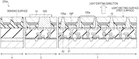
- an image display device 200 having a plurality of micro light emission elements 100 as a light source as an example.
- the image display device 200 has the plurality of micro light emission elements 100 in a pixel region 1 .
- the image display device 200 is provided with a drive circuit substrate 50 with which current is supplied to the micro light emission elements 100 to emit light. Light emitted from the micro light emission elements 100 is emitted to a side opposite to the drive circuit substrate 50 .
- a wavelength conversion layer may be disposed on the light emitting side of the micro light emission elements 100 , since they are not directly related to the present disclosure, they are not illustrated in the drawings.
- the drive circuit substrate 50 is configured with a micro light emission element drive circuit, a row selection circuit, a column signal output circuit, an image processing circuit, an input/output circuit, and the like.
- the micro light emission element drive circuit controls current supplied to each of the micro light emission elements 100 .
- the row selection circuit selects each row of the micro light emission elements 100 arranged in a two-dimensional matrix.
- the column signal output circuit outputs light emission signals to each column of the micro light emission elements 100 .
- the image processing circuit calculates a light emission signal based on an input signal.
- a P-drive electrode 51 (second drive electrode) and an N-drive electrode 52 (first drive electrode) for coupling to the micro light emission element 100 are disposed.
- Surfaces of the P-drive electrode 51 and the N-drive electrode 52 are configured to be planarized.
- the drive circuit substrate 50 is generally a silicon substrate (semiconductor substrate) on which a large-scale integrated circuit (LSI) is formed, and since it can be manufactured by a known technology, its function and configuration will not be described in detail.
- LSI large-scale integrated circuit
- a cross section along a substrate surface of the micro light emission element 100 can have various planar shapes such as a rectangle, a polygon, a circle, and an ellipse, and it is assumed that the maximum length in a direction along the substrate surface is about 60 ⁇ m or less.
- the image display element 200 it is assumed that three thousand or more micro light emission elements 100 are integrated into a pixel region 1 .
- the micro light emission element 100 includes a compound semiconductor 14 as a light emitting body, and generally, an N-side layer 11 (first conductive layer), a light emission layer 12 , and a P-side layer 13 (second conductive layer) are laminated in this order.
- the compound semiconductor 14 is, for example, a nitride semiconductor (AlInGaN-based) in a micro LED element that emits light in a wavelength band from ultraviolet to green color.
- the compound semiconductor 14 is AlInGaP-based when emitting light in a wavelength band from yellowish green color to red color.
- the compound semiconductor 14 is an AlGaAs-based or GaAs-based in a wavelength band from red color to infrared.
- the compound semiconductor 14 which configures the micro light emission element 100 , a configuration in which the N-side layer 11 is disposed on the light emitting side will be described.
- the compound semiconductor 14 may have a configuration in which the P-side layer 13 is disposed on the light emitting side.
- each of the N-side layer 11 , the light emission layer 12 , and the P-side layer 13 is normally optimized to include a plurality of layers instead of a single layer, since it is not directly related to the present disclosure, the detailed structure of each layer will not be described.
- the light emission layer is interposed between the N-type layer and the P-type layer, but since the N-type layer or the P-type layer may also include a non-doped layer or a layer having a dopant with opposite conductivity in some cases, hereinafter, those are described as an N-side layer and a P-side layer.
- one image display device 200 or a part thereof will be described. However, in a manufacturing process of the image display device 200 , the process is performed on a wafer on which a plurality of image display devices 200 are arranged, and the process is complete by finally dividing the wafer into each image display device 200 .
- the image display device 200 has a configuration in which the micro light emission element 100 that emits light is stuck to the drive circuit substrate 50 on a planarized bonding surface (indicated by a thick broken line).
- the micro light emission element 100 the light emission layer 12 is isolated by an isolation trench 15 .
- a P-electrode 19 P (second electrode) coupled to the P-side layer 13 is disposed.
- an N-electrode 19 N (first electrode) coupled to the N-side layer 11 is disposed.
- the P-electrode 19 P and the N-electrode 19 N are simultaneously formed by the same process as will be described later, and thus shapes, sizes, and depths are different, but as material, interconnection materials of the same structure are used.
- the interconnection material has a multilayer structure configured with a plurality of layers such as a barrier metal layer, a main conductive layer, and a cap layer.
- the P-electrode 19 P and the N-electrode 19 N have the same multilayer structure. That is, the image display device 200 is formed in a single interconnection layer on the side of the micro light emission element 100 .
- the P-electrode 19 P and the N-electrode 19 N are made of metal materials which are in ohmic contact with the N-side layer 11 , an ohmic contact with the P-side layer 13 is performed through the P-electrode layer 10 .
- the P-electrode layer 10 is a good conductor such as indium-tin-oxide (ITO) which is a transparent conductive electrode or palladium (Pd).
- ITO indium-tin-oxide
- Pd palladium
- the P-electrode layer 10 does not necessarily have to be a continuous thin-film, and may have, for example, a structure in which palladium nanoparticles are dispersedly allocated.
- the isolation trench 15 of the micro light emission element 100 is filled with the protection layer 17 , and a surface (second surface) on a bonding surface side of the protection layer 17 is planarized.
- the P-electrode 19 P and the N-electrode 19 N are formed on the bonding surface side, and the surfaces thereof are formed in a plane substantially at the same height as the surface of the protection layer 17 .
- a surface on a bonding surface side of an insulation layer 55 on the drive circuit substrate 50 side is also planarized, and the surfaces of the P-drive electrode 51 and the surface of the N-drive electrode 52 are formed in a plane substantially at the same height as the surface of the insulation layer 55 .
- the P-electrode 19 P and the N-electrode 19 N are connected to the P-drive electrode 51 and the N-drive electrode 52 on the drive circuit substrate 50 side, respectively.
- some height difference may exist between a surface of the protection layer 17 , and surfaces of the P-electrode 19 P and the N-electrode 19 N.
- surface layers of the P-electrode 19 P and the N-electrode 19 N, and surface layers of the P-drive electrode 51 and the N-drive electrode 52 are made of the same material, for example, gold (Au), copper (Cu), nickel (Ni), or the like.
- the micro light emission elements 100 are generally arranged in a two-dimensional array when viewed from the bonding surface side. As illustrated in FIG. 2B , the P-electrode 19 P is disposed at a center portion of the micro light emission element 100 , and the N-electrode 19 N is disposed at a boundary portion thereof. At a lower portion of the N-electrode 19 N, as illustrated in FIG. 2A , an isolation trench 15 is present. Note that FIG. 1 illustrates I-I cross section in FIG. 2B . In addition, FIG. 2A illustrates a surface after forming isolation trenches 15 (state of FIG. 3B ). Furthermore, FIG. 2B illustrates a surface after forming the P-electrode 19 P and the N-electrode 19 N (state of FIG. 3E ). However, the protection layer 17 is omitted.
- a plurality of image display devices 200 can be manufactured at a time by bonding together a wafer in which a plurality of drive circuit substrates 50 are disposed and a wafer in which a plurality of micro light emission elements 100 are disposed.
- the manufacturing process of the micro light emission element 100 will be described with reference to FIGS. 3A to 3E .
- the N-side layer 11 , the light emission layer 12 , and the P-side layer 13 which constitute the compound semiconductor, are sequentially laminated on the growth substrate 9 , and the P-electrode layer 10 is further deposited.
- the isolation trenches 15 are formed by etching the P-electrode layer 10 , P-side layer 13 , light emission layer 12 , and a part of the N-side layer 11 . At this time, a part including the light emission layer 12 becomes a mesa 16 .
- the isolation trenches 15 are arranged at equal intervals in longitudinal and lateral directions, and the mesas 16 have a shape of a truncated square cone.
- the shape of the mesa 16 is not limited to a truncated square cone, and may be a truncated circular cone or other truncated polygon cones.
- a side wall of the mesa 16 is desirably inclined at about 45° ⁇ 10° with respect to a surface formed by the light emission layer 12 .
- the ratio of light traveling in a direction parallel to the light emission layer 12 is the largest. Therefore, by reflecting such light in a direction of the light emitting surface, the light output efficiency of the micro light emission element 100 can be enhanced.
- the protection layer 17 is deposited and the surface is planarized by chemical mechanical polishing (CMP).
- CMP chemical mechanical polishing
- the protection layer 17 is an insulation layer, and is, for example, made of SiO 2 , SiN, SiON, or a multilayer film of these films.
- Various film formation technologies such as a chemical vapor deposition (CVD) method, a sputtering method, and coating can be used for forming the protection layer 17 .
- a P-groove 18 P is formed on the mesa 16 , and an N-groove 18 N is formed on the isolation trench 15 .
- the P-groove 18 P has a hole shape and reaches the P-electrode layer 10 .
- the N-groove 18 N has a channel shape running in both longitudinal and lateral directions, and reaches the N-side layer 11 at a bottom portion of the isolation trench 15 .
- the P-electrode 19 P and the N-electrode 19 N are formed by filling the P-groove 18 P and the N-groove 18 N with a metal film.
- the metal film is, for example, a combination of a barrier film such as tantalum (Ta), tungsten (W), and titanium nitride (TiN), and copper.
- a combination of gold or nickel or the like with a corresponding barrier film may be used.
- a metal thin film is deposited on a substrate structure having a trench and a CMP is performed, thereby the metal thin film can remain in the trench and the surface is planarized.
- the Damascene method is one of metal interconnection formation methods of LSI, and is a thin film formation technology using a plating technology and a CMP method in combination.
- the Damascene method is referred to as a damascene skill in which a fine metal interconnection layer is implanted in an insulation layer.
- the method is focused on copper (Cu) interconnection, and a trench having an interconnection shape is formed in an insulating interlayer and is filled with a metal such as copper.
- Cu copper
- the other is called “dual Damascene interconnection method”, which is a method of filling a through hole and an interconnection trench with a metal at a time after forming the through hole and the interconnection trench.
- the Damascene method is used in combination with a CMP technology to planarize a multilayered interconnection layer.
- the process of FIGS. 3A to 3E uses the single Damascene method.
- the P-electrode 19 P is disposed on the mesa 16
- the N-electrode 19 N is disposed on the isolation trench 15
- both the P-electrode 19 P and the N-electrode 19 N are disposed on surfaces to be the bonding surface (on the same plane), and the surfaces are configured to be planarized with the same material. That is, both the P-electrode 19 P and the N-electrode 19 N surfaces are flush with each other and are made of a same material.
- the interconnection layer is configured with one layer, and it can be formed by a two-step photolithography process of forming the isolation trench 15 and the mesa 16 , and forming the P-groove 18 P and the N-groove 18 N. Therefore, the micro light emission element 100 may be manufactured with a very simple manufacturing process, and the equipment investment can be reduced and the manufacturing costs can be significantly reduced.
- the photolithography is a technology for generating patterns formed in an exposed part and in an unexposed part by exposing a surface of a substance coated with a photosensitive substance in the patterns.
- FIG. 4A is a view obtained by inverting the configuration illustrated in FIG. 3E in a top-bottom direction.
- the drive circuit substrate 50 is manufactured.
- the drive circuit substrate 50 is formed, for example, on a single crystal silicon substrate (wafer) by a usual complementary metal-oxide semiconductor (CMOS) process.
- CMOS complementary metal-oxide semiconductor
- both the micro light emission element 100 and the drive circuit substrate 50 be in a wafer state.
- the micro light emission elements 100 are divided into individual pieces by the units of the image display devices 200 , a large amount of dust is generated in a dividing process, so the dust adheres to the bonding surface in the bonding process and a problem occurs that the bonding yield significantly decreases. Such a problem does not occur if the micro light emission element 100 and the drive circuit substrate 50 are wafers.
- both wafers of a growth substrate 9 of the micro light emission element 100 and the drive circuit substrate 50 are made of the same material. This is because heating may be desirable when bonding is performed, and if both wafer materials are the same, it is possible to suppress a pattern deviation due to a difference in thermal expansion coefficient. Furthermore, it is desirable that both wafers have the same size. If the sizes are different, a useless region which is not used is generated on a larger wafer.
- the micro light emission element 100 and the drive circuit substrate 50 are stuck.
- the P-electrode 19 P and the N-electrode 19 N are precisely aligned so as to overlap with the corresponding P-drive electrode 51 and the N-drive electrode 52 , respectively.
- the two wafers are stuck to each other by plasma cleaning of the surface or activation by ion irradiation or heating or pressure, in accordance with the material of the bonding surface.
- the growth substrate 9 of the micro light emission element 100 is removed.
- various skills such as grinding, polishing, plasma etching, wet etching, wet etching of a sacrificial layer, and laser lift-off can be used.
- the micro light emission elements 100 configured with the compound semiconductor 14 are arranged on the drive circuit substrate 50 to complete the structure.
- the electrical coupling is completed between the micro light emission element 100 and the drive circuit of the drive circuit substrate 50 , and an interconnection layer may not be provided on the light emitting surface.
- a plan view of the image display device 200 is illustrated in FIG. 5A .
- a pixel region 1 is a part that emits light and actually displays an image. The above description is mostly made on the pixel region 1 .
- a dummy region 2 which is a region that does not emit light
- I/O regions 3 external coupling regions
- scribe portion 4 which separates the image display device 200 individually.
- circuits such as a row selection circuit, a column signal output circuit, an image processing circuit, and an input/output circuit other than the micro light emission element drive circuit are disposed on the drive circuit substrate 50 .
- the compound semiconductor 14 is stuck on the drive circuit substrate 50 in all of these regions. Therefore, the surface on the light emitting surface side of the image display device 200 is planarized, and the process of forming a pattern for wavelength conversion by a phosphor or a quantum dot, a color filter, a micro lens or the like can be easily performed. Since it is desirable to maintain the coupling between the compound semiconductor 14 and the drive circuit substrate 50 even in the region other than the pixel region 1 , in principle, it is desirable that the bonding surfaces of the compound semiconductor 14 side and the drive circuit substrate 50 side face each other with the same kind of materials.
- the insulation layers can be made to face each other. That is, it is possible not to provide an electrode in the dummy region 2 .
- the electrodes can be densely packed.
- the same structure as the micro light emission element 100 is formed in the dummy region 2 and used as an optical sensor. In such a case, the same structure as the pixel region 1 is disposed.
- an external coupling portion 54 is provided on the light emitting surface side of the compound semiconductor 14 .
- the external coupling portion 54 supplies an image signal, a control signal, a power source, or the like to the image display device 200 .
- An example of the external coupling portion 54 is a wire bonding pad.
- the external coupling portion 54 is coupled to a corresponding electrode on the drive circuit substrate 50 side through an external coupling electrode 19 O formed simultaneously with the N-electrode 19 N.
- the external coupling electrode 19 O may have a plurality of thin pillars similar to the N-electrode 19 N, or may be formed in a thick pillar shape.
- the N-side layer 11 of the compound semiconductor 14 is present between the external coupling electrode 19 O and the external coupling portion 54 .
- an electrode pattern such as the P-drive electrode 51 or the N-drive electrode 52 is disposed on the drive circuit substrate 50 side, but the corresponding P-electrode or N-electrode is not disposed on the compound semiconductor 14 side.
- bonding force in the region can be weakened by disposing the electrode on one side and not disposing the electrode on the other side.
- the micro light emission element 100 is of one type and is a monochrome display device.
- a pixel 5 can be configured with a blue sub-pixel 6 , a red sub-pixel 7 , and a green sub-pixel 8 to form a full color display device.
- Each sub-pixel has an individual micro light emission element.
- Each sub-pixel may be configured with a micro light emission element that emits blue light, red light, or green light, or may emit red light or green light by combining a micro light emission element that emits blue light with a wavelength conversion layer.
- an isolation trench 15 surrounds a periphery of each sub-pixel and N-electrodes 19 N are disposed on all the isolation trenches 15 .
- the isolation trench 15 surrounds the periphery of each sub-pixel
- the N-electrodes 19 N is disposed so as to cover a periphery of the pixel 5 .
- the isolation trench 15 between the sub-pixels can be narrowed.
- by enlarging the width of a mesa 16 of the sub-pixel an area of the light emission layer 12 can be expanded, current density flowing into the light emission layer 12 can be reduced, and the light emission efficiency can be improved.
- the N-electrode 19 N can be disposed only in one direction of a boundary of the pixel 5 , or as illustrated in FIG. 6D the N-electrode 19 N can also be disposed in a dot shape at the four corners of the pixel 5 . All have the same effect as FIG. 6B , and as the amount of disposition of the N-electrode 19 N decreases, the effect of improving the light emission efficiency becomes larger. In this way, although the N-electrode 19 N is disposed on the isolation trench 15 , it does not necessarily have to be disposed on the entire region of the isolation trench 15 .
- the N-electrode 19 N is provided for at least each pixel 5 since it is desirable that the interconnection resistance be uniform among the pixels 5 . Therefore, as illustrated in FIG. 6D , the configuration in which the N-electrodes 19 N are disposed at the four corners of the pixel 5 is most desirable.
- the shape of the sub-pixel is not limited to the shape illustrated in FIG. 6A , and may be, for example, the shape illustrated in FIG. 7A .
- one P-electrode 19 P is disposed to the micro light emission element 100 , but the number is not limited to one.
- two of a P-electrode 1 19 P 1 and a P-electrode 2 19 P 2 may be disposed.
- the redundant function means that a spare device is disposed as a backup and a failure device is replaced by the spare device so as to maintain the function of the entire system even when a failure occurs.
- the P-electrode layer is also divided into a P-electrode layer 1 10 - 1 and a P-electrode layer 1 10 - 2 , so that the micro light emission element 100 can be actually divided into two.
- the P-electrode 1 19 P 1 becomes defective
- the redundant function can be realized not only for the conduction defect of the electrode but also for the micro light emission element 100 .
- the number of processes of photolithography may be increased by one.
- the P-electrode is disposed on the mesa 16 having the light emission layer 12 , it is not necessarily limited to one, and a plurality of P-electrodes may be disposed.
- the present embodiment differs from Embodiment 1 in that a separation trench 20 for separating the micro light emission elements 100 a is added.
- the separation trench 20 covers the periphery of the micro light emission element 100 a to inhibit leakage of light from the micro light emission element 100 a to adjacent micro light emission elements, thereby a decrease in contrast can be inhibited.
- FIGS. 8A and 8B are the same as FIGS. 3A and 3B , respectively.
- the separation trench 20 is formed at the bottom portion of the isolation trench 15 . Thereby, each micro light emission element 100 a is separated.
- the isolation trench 15 and the separation trench 20 are filled with a protection layer 17 , and a surface is planarized by CMP.
- the P-groove 18 P and the N-groove 18 Na are formed, and the P-electrode 19 P and the N-electrode 19 Na are formed by using the Damascene method.
- the coupling between the N-electrode 19 Na and the N-side layer 11 is performed on a side wall of the N-side layer 11 formed when the separation trench 20 is formed, but the coupling method is not limited thereto.
- the bottom portion of the isolation trench 15 may be coupled to the N-electrode 19 Na without increasing the number of processes by leaving the bottom portion of the isolation trench 15 in the micro light emission element 100 a and forming the N-groove 18 Na in that portion.
- FIG. 9 A sectional view of the image display device 200 a formed in this manner is illustrated in FIG. 9 .
- FIG. 9 other than the pixel region 1 in which the micro light emission element 100 a emitting light is present, a sectional view is also illustrated for the external coupling region 3 and the scribe portion 4 .
- the P-electrode 19 P and the N-electrode 19 Na of the micro light emission element 100 a are configured with the same interconnection layer, and have a simple configuration having only one interconnection layer, thereby it can be manufactured by a simple manufacturing process.
- the metal material forming the N-electrode covers the periphery of the micro light emission element 100 a . That is, sidewalls of the micro light emission element 100 a are covered by the metal material as shown in FIG. 8F and FIG. 9 . Thereby, light emitted from the micro light emission element 100 a can be inhibited from leaking to the adjacent micro light emission elements 100 a , and the contrast can be enhanced.
- the other points are similar to those of Embodiment 1, and as in Embodiment 1, since a current path between the micro light emission element 100 a and the drive circuit substrate 50 is completed at the time of bonding, an interconnection may not be formed on a light emitting surface after the bonding.
- the N-electrode 19 N reaches the light emitting surface of the compound semiconductor 14 . Therefore, the external coupling electrode 19 O formed simultaneously can be exposed on the light emitting surface of the compound semiconductor 14 .
- the external coupling electrode 19 O may have a thick pillar shape, or may have a large number of thin pillars arranged, and can be formed in the same process as the N-electrode 19 Na.
- the external coupling portion 54 may be, for example, a pad for wire bonding or a gold bump. As described above, according to the configuration of the present embodiment, a low resistance external coupling portion 54 can be easily disposed.
- the metal electrode is not disposed on the drive circuit substrate 50 side nor on the compound semiconductor 14 side. This is because, when the image display devices 200 are separated from each other by laser dicing, it is desirable to have no metal electrode. It is also possible to combine such a scribe portion 4 with Embodiment 1.
- the present embodiment is similar to Embodiment 2 in that a micro light emission element 100 b is surrounded by a metal material, but the configuration of the metal material is different.
- FIGS. 10A to 10E illustrate a manufacturing process of the micro light emission element 100 b .
- FIGS. 10A to 10C are similar to FIGS. 3A to 3C , respectively. However, the P-electrode layer 10 is omitted.
- the protection layer 17 is etched and then the N-side layer 11 is etched to form an N-groove 18 Nb. Thereafter, as illustrated in FIG. 10E , an N-side contact electrode 21 is formed in a lower portion of the N-groove 18 Nb.
- the N-side contact electrode 21 is desirably made of a metal material having a high reflectance, such as aluminum, when in contact with the N-side layer 11 .
- the electrode used for the bonding is generally made of a material such as gold, copper, nickel, or the like.
- a light reflectance at a boundary surface is about 40% to 60%, and about half of the light is absorbed by the metal material.
- materials such as aluminum or silver have a reflectance of about 80% or more and have relatively low light absorption. Therefore, as compared with Embodiment 2, the configuration of the present embodiment can improve the light output.
- a structure in which a lower portion of the N-groove 18 Nb is filled with a metal material and an upper portion is opened as illustrated in FIG. 10E can be formed, for example, by filling the portion with the metal material using a flow sputtering method or a CVD method, and by dry etching back the surface.
- a P-groove 18 P is formed, and further, as illustrated in FIG. 11B , the P-electrode 19 P and the N-electrode 19 N are formed.
- the main materials of the P-electrode 19 P and the N-electrode 19 N are the same as those in Embodiment 1 and Embodiment 2, but in the present embodiment, the metal layer of the lowermost portion is changed to directly couple to the P-side layer 13 .
- the P-electrode layer 10 is omitted to reduce the number of processes, but the P-electrode layer 10 may not necessarily be omitted.
- the P-electrode 19 P is disposed on the mesa 16
- the N-electrode 19 N is disposed on the isolation trench 15
- both the P-electrode 19 P and the N-electrode 19 N are disposed on surfaces to be the bonding surface, and the surfaces are configured to be planarized with the same material.
- the N-electrode 19 N is configured with two layers made of different materials, and on a side in contact with the N-side layer 11 of the light emitting surface side, a material with high light reflectance is disposed.
- an image display device 200 b can be configured as in Embodiment 2.
- the N-electrode 19 N is configured with two layers made of different materials, and a material having a high light reflectance is disposed on a side in contact with the N-side layer 11 of the light emitting surface side, thereby the light output can be improved as compared with Embodiment 2.
- the present embodiment is different in that a micro light emission element 100 c is a vertical cavity surface emitting laser (VCSEL) type micro laser element. Compared to the micro LED element, a spectrum of light emitting wavelength is narrow, and display with high directivity is possible.
- VCSEL vertical cavity surface emitting laser
- FIGS. 12A to 12E are sectional views illustrating a manufacturing process of the micro light emission element 100 c.
- a first reflection layer 43 , an N-side layer 11 c , the light emission layer 12 and the P-side layer 13 are sequentially deposited on the growth substrate 9 to form a compound semiconductor 14 c.
- the first reflection layer 43 is a distributed Bragg reflector (DBR) that reflects light of an laser emission wavelength.
- DBR distributed Bragg reflector
- the first reflection layer 43 can be formed by stacking a plurality of pairs of Al x Ga (1-x) N layers and GaN layers.
- the first reflection layer 43 includes 20 layers of GaN/AlGaN pairs in which a thickness of the GaN layer is 46 nm, a thickness of the Al x Ga (1-x) N layer is 47 nm, and a total thickness of GaN/AlGaN pair is 93 nm, and has the total thickness of about 1.8 ⁇ m.
- the transparent conductive electrode layer 44 and a second reflection layer 45 are further deposited on the compound semiconductor 14 c .
- the transparent conductive electrode layer 44 is an electrode layer of indium, tin, oxide (ITO), or the like, and has a thickness of about 50 nm to 600 nm.
- the second reflection layer 45 is a DBR configured with a dielectric multilayer film.
- the second reflection layer 45 includes 10 layers of pairs of a TiO 2 thin film (thickness is 36 nm) and a SiO 2 thin film (thickness is 77 nm), and has the total thickness of about 1.1 ⁇ m.
- the reflectance of the second reflection layer 45 to blue light is higher than the reflectance of the first reflective layer 43 .
- the isolation trenches 15 are formed by a photolithography technique and a dry etching technique.
- the isolation trench 15 is formed by etching a part of a second reflection layer 45 , a part of a transparent conductive electrode layer 44 , a part of the P-side layer 13 , a part of the light emission layer 12 , and a part of the N-side layer 11 . It is not desirable to incline the side surface of the isolation trench 15 largely, as in Embodiment 1. This is because, with the laser element, the isolation trench does not emit light in a horizontal direction, thereby a reflection in a vertical direction is not compulsory.
- the isolation trenches 15 are filled with a protection layer 17 , and the surface is planarized. Further, as illustrated in FIG. 12D , an N-groove 18 N and a P-groove 18 Pc are formed.
- the N-groove 18 N reaches the N-side layer 11 c at the bottom portion of the isolation trench 15 by etching the protection layer 17 .
- the P-groove 18 Pc reaches the transparent conductive electrode layer 44 by etching the protection layer 17 and the second reflection layer 45 .
- the P-electrode 19 Pc and the N-electrode 19 N are formed.
- the P-electrode 19 Pc is formed on the light emission layer, it is desirable that the P-electrode 19 Pc be disposed not on the center but on the outer peripheral portion with respect to the region where the light emission layer 12 exists. This is because the P-electrode 19 Pc penetrates the second reflection layer 45 thereby the light emission of the laser element is inhibited.
- the P-electrode 19 Pc is disposed on the light emission layer 12
- the N-electrode 19 N is disposed on the isolation trench 15
- both the P-electrode 19 Pc and the N-electrode 19 N are formed in a single interconnection layer and disposed on surfaces to be the bonding surface, and the surfaces are configured to be planarized with the same material.
- an image display device 200 c can be configured as in Embodiment 1.
- the effect similar to Embodiment 1 is realizable.
- the spectral width of the light emitting wavelength can be narrowed, and the directivity can be increased.
- the present embodiment is different from Embodiment 2 in that a micro light emission element 100 d is not completely separated by the separation trench 20 , and the metal layer does not directly cover the side wall of the N-side layer of the micro light emission element 100 d.
- FIGS. 13A and 13B are the same as FIGS. 8A and 8B in Embodiment 2, respectively.
- the separation trench 20 is formed, but it is different from FIG. 8C .
- a residual N-portion 22 remains in a part.
- a plan view of this state is illustrated in FIG. 14A , and the residual N-portion 22 is disposed between two among the four corners of the micro light emission element 100 d configuring each sub-pixel.
- the residual N-portion 22 is a portion where the N-side layer 11 and the N-electrode 19 N are coupled, and the disposition thereof may not be limited to the location of FIG. 14A and may be the center of a side of the micro light emission element 100 d.
- a protection layer 23 is deposited on the entire surface.
- the protection layer 23 is an insulation layer of the same type as the protection layer 17 . It is desirable that the protection layer 23 is a transparent insulation layer.
- a P-contact hole 24 P and an N-contact hole 24 N are formed in the protection layer 23 .
- the P-contact hole 24 P is disposed on the P-electrode layer 10
- the N-contact hole 24 N is disposed on the residual N-portion 22 .
- the disposition of the contact holes is illustrated in FIG. 14B .
- a metal material is deposited, and a surface is dry etched back or polished by CMP, then the metal material is left in a recessed portion, thereby the P-electrode 19 P is formed in the P-contact hole 24 P. Further, an N-electrode 19 Nd is formed in the N-contact hole 24 N and between the micro light emission elements 100 d . Furthermore, the metal material filling a gap 26 portion becomes the reflective light shielding portion 27 .
- the side wall of the N-side layer 11 and the side wall of the mesa 16 are covered with the protection layer 23 , and a reflective metal material is disposed outside the protection layer 23 to shield the micro light emission elements from outgoing and incoming light.
- a plan view of this state is illustrated in FIG. 14C .
- the P-electrode 19 P and the N-electrode 19 Nd of the micro light emission element 100 d are configured with the same interconnection layer, and have a simple configuration having only one interconnection layer, thereby it can be manufactured by a simple manufacturing process.
- an image display device 200 d can be configured as in Embodiment 2.
- the micro light emission element 100 d is partially coupled to the micro light emission element via the residual N-portion 22 .
- the coupling portion is very small and the other part is covered by the light shielding portion 27 , light leakage is reduced and a decrease in contrast can be significantly suppressed.
- the interconnection layer is not exposed to the light emitting surface.
- the metal material which becomes the light shielding portion 27 is covered with the protection layer 23 .
- the coupling resistance between the metal material and the external coupling portion 54 can be reduced by etching the protection layer 23 present at a boundary surface with the growth substrate 9 .
- the present embodiment has a configuration in which Embodiment 5 and Embodiment 3 are combined.
- the manufacturing process of the micro light emission element 100 e will be described with reference to FIG. 15A to FIG. 17B .
- FIGS. 15A and 15B are the same as FIGS. 8A and 8B in Embodiment 2, respectively.
- a residual N-portion 22 remains in a part.
- a plan view of this state is illustrated in FIG. 17A , and a residual N-portion 22 is disposed between two adjacent micro light emission elements 100 e .
- a sectional view taken along line XVC-XVC part in FIG. 17A is illustrated in FIG. 15C .
- the residual N-portion 22 is a portion where the N-side layer 11 and the N-electrode 19 N are coupled, and the disposition thereof may not be limited to the location in FIG. 17A and may be a corner of the micro light emission element 100 e.
- a protection layer 23 is deposited on the entire surface.
- This process is a simple process without the need for planarization by CMP.
- a P-contact hole 24 P and an N-contact hole 24 N are formed in the protection layer 23 .
- the P-contact hole 24 P is disposed on the P-electrode layer 10
- the N-contact hole 24 N is disposed on the residual N-portion 22 .
- a metal material is deposited, and a surface is dry etched back or polished by CMP, then the metal material is left in a recessed portion, thereby a lower P-electrode 25 P is formed in the P-contact hole 24 P.
- a lower N-electrode 25 N is formed in the N-contact hole 24 N.
- the metal material filling a gap 26 portion becomes the reflective light shielding portion 27 .
- a plan view of this state is illustrated in FIG. 17B .
- the metal material deposited in the present process is made of a material having a high reflectance to the light emitted from the micro light emission element 100 e .
- the metal material is aluminum or silver.
- the side wall of the N-side layer 11 and the side wall of the mesa 16 are covered with the protection layer 23 , and a reflective metal material is disposed outside the protection layer 23 to shield the micro light emission elements 100 e from outgoing and incoming light.
- a protection layer 17 e is deposited, and the surface is planarized by CMP.
- the P-groove 18 P and the N-groove 18 N are formed as in Embodiment 1, and the P-electrode 19 P and the N-electrode 19 N are formed by using the Damascene method.
- FIGS. 16B and 16C is a sectional view taken along line XVIB, XVIC-XVIB, XVIC part in FIG. 17B . Since it is sufficient that the N-groove 18 N is present on the lower N-electrode 25 N, a degree of freedom in disposition increases, and disposing at a point where a distance to the P-electrode 19 P is maximized as illustrated in FIG. 17B , it is possible to reduce a short circuit defect.
- the P-electrode 19 P is disposed on the mesa 16
- the N-electrode 19 N is disposed on the isolation trench 15
- both the P-electrode 19 P and the N-electrode 19 N are disposed on surfaces to be the bonding surface, and the surfaces are configured to be planarized with the same material.
- an image display device 200 e can be configured as in Embodiment 2.
- the micro light emission element 100 e is partially coupled to the micro light emission element via the residual N-portion 22 .
- the coupling portion is very small and the other part is covered by the light shielding portion 27 , light leakage is reduced and a decrease in contrast can be significantly suppressed.
- Embodiment 2 Therefore the effect similar to Embodiment 2 is realizable. Furthermore, in the configuration of the present embodiment, by covering the micro light emission element 100 e with a transparent insulation layer and disposing a metal with high reflectance on the outside, the reflectance can be improved and the light output can be further improved.
- the interconnection layer is not exposed to the light emitting surface.
- the metal material which becomes the light shielding portion 27 is covered with the protection layer 23 .
- the coupling resistance between the metal material and the external coupling portion 54 can be reduced by etching the protection layer 23 present at a boundary surface with the growth substrate 9 .
- a micro light emission element includes a compound semiconductor in which a first conductive layer, a light emission layer, and a second conductive layer having a conductivity type opposite to a conductivity type of the first conductive layer are sequentially laminated from a side of a light emitting surface, in which a first electrode coupled to the first conductive layer and a second electrode coupled to the second conductive layer are disposed on another surface opposite to the light emitting surface, the second electrode is disposed on the light emission layer, the first electrode is disposed in an isolation region which is a boundary region of the micro light emission element and isolates the light emission layer from a light emission layer of another micro light emission element, and a surface of the first electrode on a side of the other surface side and a surface of the second electrode on the side of the other surface side are flush with each other and are made of an identical material.
- micro light emission element according to aspect 2 of the present disclosure may be formed of a single interconnection layer, in the above-mentioned aspect 1.
- each of the first electrode and the second electrode is formed on the same plane (bonding surface).
- the first electrode and the second electrode can be simultaneously stuck to a first drive electrode and a second drive electrode of the drive circuit substrate, respectively.
- a first metal material is disposed on the light emitting surface side, and a second metal material is disposed on the other surface side, and the first metal material has a higher reflectance as compared to the second metal material.
- the micro light emission element in the above-mentioned aspect 1, may be coupled to at least part of the other micro light emission element.
- the micro light emission element in the above-mentioned aspect 1, the micro light emission element may be completely separated from the other micro light emission element.
- the first electrode may cover a periphery of the micro light emission element.
- the first electrode may reach the light emitting surface.
- the micro light emission element may be a light emitting diode, in which a side wall of an isolation trench isolating the light emission layer from the light emission layer of the other micro light emission element may be inclined at a range of 45° ⁇ 10° with respect to a surface of the light emission layer.
- the micro light emission element in the above-mentioned aspect 1, may have a plurality of second electrodes coupled to the second conductive layer.
- an N-side layer and a side wall of a mesa of the micro light emission element may be covered with a protection layer, and a reflective metal material may be disposed outside the protection layer.
- the metal material may be the first electrode.
- an N-side layer and a side wall of a mesa of the micro light emission element may be covered with a protection layer, and the second metal material may be disposed outside the protection layer.
- the micro light emission element may have a laser diode structure of a vertical resonator surface light emitting laser.
- the micro light emission element may be disposed on a drive circuit substrate, and the second electrode and the first electrode of the micro light emission element may be coupled to a corresponding second drive electrode and a corresponding first drive electrode on the drive circuit substrate, respectively.
- the compound semiconductor may be disposed on an entire surface of the image display device.
- an external coupling portion may be provided on the light emitting surface of the compound semiconductor.
- the image display device may have a region where an electrode is disposed on one of a side of the micro light emission element and a side of the drive circuit substrate, at a bonding surface of the micro light emission element and the drive circuit substrate.
- a method of forming a micro light emission element includes a process of sequentially depositing a first conductive layer, a light emission layer, and a second conductive layer having a conductivity type opposite to a conductivity type of the first conductive layer on a growth substrate and growing a compound semiconductor, a process of forming an isolation trench that isolates the light emission layer of the compound semiconductor for each micro light emission element on the growth substrate, a process of depositing a protection layer on the isolation trench and planarizing a surface of the isolation trench, and a process of forming a second electrode coupled to the second conductive layer on the light emission layer, and forming a first electrode coupled to the first conductive layer on the isolation trench, in which the respective surfaces of the second electrode and the first electrode are formed to be planarized.
- a method of forming an image display device includes a process of forming a micro light emission element by using the method of forming a micro light emission element according to aspect 14, a process of forming, on a semiconductor substrate, a drive circuit that drives the micro light emission element, a process of bonding the micro light emission element to a surface of the semiconductor substrate, and a process of removing the growth substrate of the micro light emission element.
- the micro light emission element has a compound semiconductor in which a first conductive layer, a light emission layer, and a second conductive layer having a conductivity type opposite to a conductivity type of the first conductive layer are sequentially laminated from a side of a light emitting surface (first surface), in which the light emission layer of the compound semiconductor is divided for each micro light emission element, a second electrode coupled to the second conductive layer and a first electrode coupled to the first conductive layer are disposed on another surface (second surface) opposite to the light emitting surface (first surface) of the micro light emission element, the second electrode is disposed on the light emission layer, the first electrode is disposed in an isolation region, and surfaces of the first electrode and the second electrode are made of a same material and are configured planarized.
- the micro light emission element may be coupled to an adjacent micro light emission element.
- micro light emission element in the micro light emission element according to an aspect of the present disclosure, most part of the micro light emission element may be separated from the adjacent micro light emission element.
- the micro light emission element may be completely separated from the adjacent micro light emission element.
- the second electrode may cover most parts of a periphery of the micro light emission element.
- the first electrode may reach a first surface.
- a first metal material in the first electrode, may be disposed on a first surface side and a second metal material may be disposed on a second surface side, and the first metal material may have a higher reflectance as compared to the second metal material.
- the micro light emission element may be a light emitting diode, and a side wall of an isolation trench isolating the light emission layer may be inclined at a range of 45° ⁇ 10° with respect to a surface of the light emission layer.
- the micro light emission element may have a plurality of second electrodes coupled to the second conductive layer.
- the micro light emission element may have a VCSEL type laser diode structure.
- the micro light emission element may be disposed on a drive circuit substrate, and the second electrode and the first electrode of the micro light emission element may be coupled to a corresponding second drive electrode and a corresponding first drive electrode on the drive circuit substrate, respectively.
- a compound semiconductor may be disposed on an entire surface of the image display device.
- an external coupling portion may be provided on the first surface of the compound semiconductor.
- the image display device may have a region where an electrode is disposed on one of the side of the micro light emission element and a side of the drive circuit substrate, at a bonding surface of the micro light emission element and the drive circuit substrate.
- a method of forming a micro light emission element may include a process of sequentially depositing a first conductive layer, a light emission layer, and a second conductive layer having a conductivity type opposite to a conductivity type of the first conductive layer on a growth substrate and growing a compound semiconductor, a process of forming an isolation trench that isolates a light emission layer of the compound semiconductor for each micro light emission element on the growth substrate, a process of depositing a protection layer on the isolation trench and planarizing a surface of the isolation trench, and a process of forming a second electrode coupled to the second conductive layer on the light emission layer, and forming a first electrode coupled to the first conductive layer on the isolation trench, in which at least surfaces of the second electrode and the first electrode may be formed at the same time to be planarized.
- a method of forming an image display device may include a process of forming a micro light emission element by using the method of forming a micro light emission element, a process of forming, on a semiconductor substrate, a drive circuit that drives the micro light emission element, a process of bonding the micro light emission element to a surface of the semiconductor substrate, and a process of removing the growth substrate of the micro light emission element.
Landscapes
- Physics & Mathematics (AREA)
- Condensed Matter Physics & Semiconductors (AREA)
- General Physics & Mathematics (AREA)
- Electromagnetism (AREA)
- Optics & Photonics (AREA)
- Engineering & Computer Science (AREA)
- Microelectronics & Electronic Packaging (AREA)
- Computer Hardware Design (AREA)
- Power Engineering (AREA)
- Led Devices (AREA)
- Manufacturing & Machinery (AREA)
- Devices For Indicating Variable Information By Combining Individual Elements (AREA)
- Semiconductor Lasers (AREA)
- Led Device Packages (AREA)
Abstract
Description
Claims (20)
Priority Applications (1)
| Application Number | Priority Date | Filing Date | Title |
|---|---|---|---|
| US16/929,817 US11296144B2 (en) | 2018-05-21 | 2020-07-15 | Image display device |
Applications Claiming Priority (5)
| Application Number | Priority Date | Filing Date | Title |
|---|---|---|---|
| JP2018-097246 | 2018-05-21 | ||
| JPJP2018-097246 | 2018-05-21 | ||
| JP2018097246A JP7105612B2 (en) | 2018-05-21 | 2018-05-21 | IMAGE DISPLAY DEVICE AND METHOD OF FORMING THE SAME |
| US16/414,041 US10763303B2 (en) | 2018-05-21 | 2019-05-16 | Micro light emission element and image display device |
| US16/929,817 US11296144B2 (en) | 2018-05-21 | 2020-07-15 | Image display device |
Related Parent Applications (1)
| Application Number | Title | Priority Date | Filing Date |
|---|---|---|---|
| US16/414,041 Continuation US10763303B2 (en) | 2018-05-21 | 2019-05-16 | Micro light emission element and image display device |
Publications (2)
| Publication Number | Publication Date |
|---|---|
| US20200350362A1 US20200350362A1 (en) | 2020-11-05 |
| US11296144B2 true US11296144B2 (en) | 2022-04-05 |
Family
ID=68533394
Family Applications (2)
| Application Number | Title | Priority Date | Filing Date |
|---|---|---|---|
| US16/414,041 Active US10763303B2 (en) | 2018-05-21 | 2019-05-16 | Micro light emission element and image display device |
| US16/929,817 Active US11296144B2 (en) | 2018-05-21 | 2020-07-15 | Image display device |
Family Applications Before (1)
| Application Number | Title | Priority Date | Filing Date |
|---|---|---|---|
| US16/414,041 Active US10763303B2 (en) | 2018-05-21 | 2019-05-16 | Micro light emission element and image display device |
Country Status (3)
| Country | Link |
|---|---|
| US (2) | US10763303B2 (en) |
| JP (1) | JP7105612B2 (en) |
| CN (1) | CN110518107B (en) |
Families Citing this family (38)
| Publication number | Priority date | Publication date | Assignee | Title |
|---|---|---|---|---|
| WO2018137139A1 (en) * | 2017-01-24 | 2018-08-02 | Goertek. Inc | Micro-led device, display apparatus and method for manufacturing a micro-led device |
| TWI707491B (en) | 2019-12-04 | 2020-10-11 | 錼創顯示科技股份有限公司 | Micro light emitting diode display panel |
| JP7348520B2 (en) * | 2018-12-25 | 2023-09-21 | 日亜化学工業株式会社 | Light emitting device and display device |
| JP7274929B2 (en) | 2019-05-13 | 2023-05-17 | 株式会社ジャパンディスプレイ | Display device |
| CN110896121B (en) * | 2019-12-04 | 2021-09-07 | 錼创显示科技股份有限公司 | Miniature LED Display Panel |
| CN111048548A (en) * | 2019-12-30 | 2020-04-21 | 深圳市奥视微科技有限公司 | Microdisplay device and projection system |
| WO2021140871A1 (en) * | 2020-01-08 | 2021-07-15 | スタンレー電気株式会社 | Vertical-resonator-type light-emitting element |
| US11282815B2 (en) | 2020-01-14 | 2022-03-22 | Micron Technology, Inc. | Methods of forming microelectronic devices, and related microelectronic devices and electronic systems |
| US11476390B2 (en) * | 2020-01-31 | 2022-10-18 | Ostendo Technologies, Inc. | III-V light emitting device with pixels enabling lower cost through-layer vias |
| JP7349393B2 (en) * | 2020-03-10 | 2023-09-22 | シャープ福山レーザー株式会社 | image display element |
| GB2593699B (en) * | 2020-03-30 | 2022-10-26 | Plessey Semiconductors Ltd | Monolithic LED pixel |
| FR3109018A1 (en) * | 2020-04-06 | 2021-10-08 | Commissariat A L'energie Atomique Et Aux Energies Alternatives | DEVICE WITH PHOTO-EMITTING AND / OR PHOTO-RECEIVING DIODES |
| CN115552745A (en) * | 2020-05-21 | 2022-12-30 | 索尼半导体解决方案公司 | Electronic device |
| TWI737484B (en) * | 2020-06-05 | 2021-08-21 | 友達光電股份有限公司 | Display apparatus |
| US11699652B2 (en) | 2020-06-18 | 2023-07-11 | Micron Technology, Inc. | Microelectronic devices and electronic systems |
| US11335602B2 (en) | 2020-06-18 | 2022-05-17 | Micron Technology, Inc. | Methods of forming microelectronic devices, and related microelectronic devices and electronic systems |
| US11557569B2 (en) | 2020-06-18 | 2023-01-17 | Micron Technology, Inc. | Microelectronic devices including source structures overlying stack structures, and related electronic systems |
| US11705367B2 (en) | 2020-06-18 | 2023-07-18 | Micron Technology, Inc. | Methods of forming microelectronic devices, and related microelectronic devices, memory devices, electronic systems, and additional methods |
| US11563018B2 (en) | 2020-06-18 | 2023-01-24 | Micron Technology, Inc. | Microelectronic devices, and related methods, memory devices, and electronic systems |
| US11380669B2 (en) * | 2020-06-18 | 2022-07-05 | Micron Technology, Inc. | Methods of forming microelectronic devices |
| WO2021260787A1 (en) * | 2020-06-23 | 2021-12-30 | 三菱電機株式会社 | Self-luminous device, liquid crystal display device, and manufacturing method for self-luminous device |
| JP2022019455A (en) | 2020-07-17 | 2022-01-27 | ソニーグループ株式会社 | Light-emitting device and image display device |
| US11417676B2 (en) | 2020-08-24 | 2022-08-16 | Micron Technology, Inc. | Methods of forming microelectronic devices and memory devices, and related microelectronic devices, memory devices, and electronic systems |
| US11825658B2 (en) | 2020-08-24 | 2023-11-21 | Micron Technology, Inc. | Methods of forming microelectronic devices and memory devices |
| WO2022054852A1 (en) * | 2020-09-10 | 2022-03-17 | ローム株式会社 | Semiconductor light emitting device and semiconductor unit |
| FR3114685B1 (en) * | 2020-09-30 | 2024-12-13 | Aledia | Optoelectronic device |
| WO2022109989A1 (en) * | 2020-11-27 | 2022-06-02 | 苏州晶湛半导体有限公司 | Gan-based laser and manufacturing method therefor |
| JP7517970B2 (en) * | 2020-12-02 | 2024-07-17 | シャープ福山レーザー株式会社 | Image display element |
| US11751408B2 (en) | 2021-02-02 | 2023-09-05 | Micron Technology, Inc. | Methods of forming microelectronic devices, and related microelectronic devices, memory devices, and electronic systems |
| CN113299679B (en) * | 2021-05-20 | 2024-06-07 | 錼创显示科技股份有限公司 | Light emitting diode micro display device |
| TWI811680B (en) | 2021-05-20 | 2023-08-11 | 錼創顯示科技股份有限公司 | Light-emitting diode micro display device |
| US20230049007A1 (en) * | 2021-08-13 | 2023-02-16 | Intel Corporation | Structures for micro led laser release |
| TWI774532B (en) * | 2021-08-24 | 2022-08-11 | 友達光電股份有限公司 | Semiconductor apparatus |
| CN113948618B (en) * | 2021-12-22 | 2022-04-22 | 南昌凯捷半导体科技有限公司 | A mini/micro LED chip using Damascus technology and its manufacturing method |
| KR20230105442A (en) * | 2022-01-04 | 2023-07-11 | 삼성전자주식회사 | Display apparatus |
| DE112023003490T5 (en) * | 2022-08-19 | 2025-07-03 | Sony Semiconductor Solutions Corporation | LIGHT EMISSION DEVICE |
| WO2025081419A1 (en) * | 2023-10-19 | 2025-04-24 | Jade Bird Display (shanghai) Limited | A micro led display panel |
| US20250275318A1 (en) * | 2024-02-23 | 2025-08-28 | Lumileds Llc | High efficient led pixel array with optimized n-contact design |
Citations (7)
| Publication number | Priority date | Publication date | Assignee | Title |
|---|---|---|---|---|
| JP2002141492A (en) | 2000-10-31 | 2002-05-17 | Canon Inc | Light emitting diode display panel and method of manufacturing the same |
| US20080031295A1 (en) | 2004-04-13 | 2008-02-07 | Akimasa Tanaka | Semiconductor Light Emitting Element and Manufacturing Method Thereof |
| US20090127568A1 (en) | 2006-07-05 | 2009-05-21 | Yoshitaka Kinoshita | Semiconductor light emitting element and method for fabricating the same |
| US20170069609A1 (en) | 2015-09-04 | 2017-03-09 | Hong Kong Beida Jade Bird Display Limited | Semiconductor apparatus and method of manufacturing the same |
| US20170179192A1 (en) | 2015-12-21 | 2017-06-22 | Hong Kong Beida Jade Bird Display Limited | Semiconductor Devices with Integrated Thin-Film Transistor Circuitry |
| US20180190672A1 (en) * | 2017-01-03 | 2018-07-05 | Innolux Corporation | Display device |
| US20190181300A1 (en) | 2016-06-20 | 2019-06-13 | Lg Innotek Co., Ltd. | Semiconductor device |
Family Cites Families (13)
| Publication number | Priority date | Publication date | Assignee | Title |
|---|---|---|---|---|
| CN101485001B (en) * | 2006-05-01 | 2011-02-02 | 三菱化学株式会社 | Integrated semiconductor light emitting device and manufacturing method thereof |
| JP2013232503A (en) * | 2012-04-27 | 2013-11-14 | Toshiba Corp | Semiconductor light-emitting device |
| US9768345B2 (en) * | 2013-12-20 | 2017-09-19 | Apple Inc. | LED with current injection confinement trench |
| JP2015156431A (en) * | 2014-02-20 | 2015-08-27 | スタンレー電気株式会社 | Semiconductor light emitting element and semiconductor light emitting device |
| US9831387B2 (en) * | 2014-06-14 | 2017-11-28 | Hiphoton Co., Ltd. | Light engine array |
| US9698134B2 (en) * | 2014-11-27 | 2017-07-04 | Sct Technology, Ltd. | Method for manufacturing a light emitted diode display |
| CN107408604B (en) * | 2015-04-03 | 2019-07-09 | 创光科学株式会社 | Nitride semiconductor ultraviolet light emitting element and nitride semiconductor ultraviolet light emitting device |
| DE102015108532A1 (en) * | 2015-05-29 | 2016-12-01 | Osram Opto Semiconductors Gmbh | Display device with a plurality of separately operable pixels |
| DE102015119353B4 (en) * | 2015-11-10 | 2024-01-25 | OSRAM Opto Semiconductors Gesellschaft mit beschränkter Haftung | Optoelectronic semiconductor component and method for producing an optoelectronic semiconductor component |
| CN112289821A (en) * | 2016-04-14 | 2021-01-29 | 群创光电股份有限公司 | display device |
| KR102566499B1 (en) * | 2016-05-26 | 2023-08-11 | 엘지이노텍 주식회사 | Light emitting device |
| CN106653961A (en) * | 2016-12-20 | 2017-05-10 | 合肥彩虹蓝光科技有限公司 | Method of manufacturing micro LED chip with flip structure |
| CN107705713B (en) * | 2017-10-13 | 2019-12-27 | 上海天马微电子有限公司 | Display panel and display device |
-
2018
- 2018-05-21 JP JP2018097246A patent/JP7105612B2/en active Active
-
2019
- 2019-05-15 CN CN201910402576.3A patent/CN110518107B/en active Active
- 2019-05-16 US US16/414,041 patent/US10763303B2/en active Active
-
2020
- 2020-07-15 US US16/929,817 patent/US11296144B2/en active Active
Patent Citations (8)
| Publication number | Priority date | Publication date | Assignee | Title |
|---|---|---|---|---|
| JP2002141492A (en) | 2000-10-31 | 2002-05-17 | Canon Inc | Light emitting diode display panel and method of manufacturing the same |
| US20080031295A1 (en) | 2004-04-13 | 2008-02-07 | Akimasa Tanaka | Semiconductor Light Emitting Element and Manufacturing Method Thereof |
| US20090127568A1 (en) | 2006-07-05 | 2009-05-21 | Yoshitaka Kinoshita | Semiconductor light emitting element and method for fabricating the same |
| CN101473457A (en) | 2006-07-05 | 2009-07-01 | 松下电器产业株式会社 | Semiconductor light emitting element and method for fabricating the same |
| US20170069609A1 (en) | 2015-09-04 | 2017-03-09 | Hong Kong Beida Jade Bird Display Limited | Semiconductor apparatus and method of manufacturing the same |
| US20170179192A1 (en) | 2015-12-21 | 2017-06-22 | Hong Kong Beida Jade Bird Display Limited | Semiconductor Devices with Integrated Thin-Film Transistor Circuitry |
| US20190181300A1 (en) | 2016-06-20 | 2019-06-13 | Lg Innotek Co., Ltd. | Semiconductor device |
| US20180190672A1 (en) * | 2017-01-03 | 2018-07-05 | Innolux Corporation | Display device |
Non-Patent Citations (2)
| Title |
|---|
| Non-Final Office Action dated Mar. 5, 2020 for U.S. Appl. No. 16/414,041. |
| Notice of Allowance and Fee(s) Due dated May 12, 2020 for U.S. Appl. No. 16/414,041. |
Also Published As
| Publication number | Publication date |
|---|---|
| US10763303B2 (en) | 2020-09-01 |
| JP7105612B2 (en) | 2022-07-25 |
| CN110518107A (en) | 2019-11-29 |
| US20200350362A1 (en) | 2020-11-05 |
| CN110518107B (en) | 2022-11-08 |
| JP2019204823A (en) | 2019-11-28 |
| US20190355786A1 (en) | 2019-11-21 |
Similar Documents
| Publication | Publication Date | Title |
|---|---|---|
| US11296144B2 (en) | Image display device | |
| US10763249B2 (en) | Image display device | |
| US11289634B2 (en) | Image display element | |
| US11581464B2 (en) | Photo-emitting and/or photo-receiving diode array device | |
| CN111863854A (en) | Image display element | |
| JP7590074B2 (en) | METHOD FOR PRODUCING INTEGRATED STRUCTURE FOR OPTOELECTRONIC DEVICE AND INTEGRATED STRUCTURE FOR OPTOELECTRONIC DEVICE | |
| CN113972232A (en) | Ultra-compact LED projector | |
| CN116565103A (en) | Micro LED micro display chip and manufacturing method thereof | |
| US11973174B2 (en) | LED displays fabricated using hybrid bonding | |
| TWI796658B (en) | Monolithic electronic device, test substrate and method of forming and testing the same | |
| US20240313182A1 (en) | Light emitting device and display apparatus having the same | |
| CN120113371A (en) | Light emitting device, method for manufacturing display device, and image display device | |
| CN118901147A (en) | Light emitting device, method for manufacturing light emitting device, and image display device | |
| US20260033399A1 (en) | Led unit for display and display apparatus having the same | |
| US20240072014A1 (en) | Micro-light emitting diode display and methods of manufacturing and operating the same | |
| WO2025134553A1 (en) | Light emitting device and image display device | |
| CN119967989A (en) | A micro light emitting diode chip and a construction method thereof | |
| WO2025205907A1 (en) | Light-emitting device and image display device | |
| WO2024176784A1 (en) | Light emitting device and image display device | |
| CN121335333A (en) | Light-emitting chip and preparation method thereof | |
| KR20260007646A (en) | Display device and method for manufacturing a display device | |
| CN121001487A (en) | A stacked full-color MicroLED device | |
| WO2023180236A1 (en) | Method for forming resonant cavity light emitting elements and optical device using the same | |
| CN120435933A (en) | Light-emitting device and image display device |
Legal Events
| Date | Code | Title | Description |
|---|---|---|---|
| AS | Assignment |
Owner name: SHARP KABUSHIKI KAISHA, JAPAN Free format text: ASSIGNMENT OF ASSIGNORS INTEREST;ASSIGNOR:IGUCHI, KATSUJI;REEL/FRAME:053219/0177 Effective date: 20190410 |
|
| FEPP | Fee payment procedure |
Free format text: ENTITY STATUS SET TO UNDISCOUNTED (ORIGINAL EVENT CODE: BIG.); ENTITY STATUS OF PATENT OWNER: LARGE ENTITY |
|
| STPP | Information on status: patent application and granting procedure in general |
Free format text: DOCKETED NEW CASE - READY FOR EXAMINATION |
|
| STPP | Information on status: patent application and granting procedure in general |
Free format text: NON FINAL ACTION MAILED |
|
| STPP | Information on status: patent application and granting procedure in general |
Free format text: RESPONSE TO NON-FINAL OFFICE ACTION ENTERED AND FORWARDED TO EXAMINER |
|
| STPP | Information on status: patent application and granting procedure in general |
Free format text: AWAITING TC RESP, ISSUE FEE PAYMENT VERIFIED |
|
| STPP | Information on status: patent application and granting procedure in general |
Free format text: PUBLICATIONS -- ISSUE FEE PAYMENT VERIFIED |
|
| STCF | Information on status: patent grant |
Free format text: PATENTED CASE |
|
| AS | Assignment |
Owner name: SHARP FUKUYAMA LASER CO., LTD., JAPAN Free format text: ASSIGNMENT OF ASSIGNORS INTEREST;ASSIGNOR:SHARP KABUSHIKI KAISHA;REEL/FRAME:071863/0508 Effective date: 20250701 |
|
| MAFP | Maintenance fee payment |
Free format text: PAYMENT OF MAINTENANCE FEE, 4TH YEAR, LARGE ENTITY (ORIGINAL EVENT CODE: M1551); ENTITY STATUS OF PATENT OWNER: LARGE ENTITY Year of fee payment: 4 |