JP2022019455A - Light-emitting device and image display device - Google Patents
Light-emitting device and image display device Download PDFInfo
- Publication number
- JP2022019455A JP2022019455A JP2020123307A JP2020123307A JP2022019455A JP 2022019455 A JP2022019455 A JP 2022019455A JP 2020123307 A JP2020123307 A JP 2020123307A JP 2020123307 A JP2020123307 A JP 2020123307A JP 2022019455 A JP2022019455 A JP 2022019455A
- Authority
- JP
- Japan
- Prior art keywords
- light emitting
- light
- emitting device
- wavelength conversion
- conversion unit
- Prior art date
- Legal status (The legal status is an assumption and is not a legal conclusion. Google has not performed a legal analysis and makes no representation as to the accuracy of the status listed.)
- Pending
Links
Images


Classifications
-
- H—ELECTRICITY
- H01—ELECTRIC ELEMENTS
- H01L—SEMICONDUCTOR DEVICES NOT COVERED BY CLASS H10
- H01L33/00—Semiconductor devices with at least one potential-jump barrier or surface barrier specially adapted for light emission; Processes or apparatus specially adapted for the manufacture or treatment thereof or of parts thereof; Details thereof
- H01L33/48—Semiconductor devices with at least one potential-jump barrier or surface barrier specially adapted for light emission; Processes or apparatus specially adapted for the manufacture or treatment thereof or of parts thereof; Details thereof characterised by the semiconductor body packages
- H01L33/50—Wavelength conversion elements
- H01L33/508—Wavelength conversion elements having a non-uniform spatial arrangement or non-uniform concentration, e.g. patterned wavelength conversion layer, wavelength conversion layer with a concentration gradient of the wavelength conversion material
-
- G—PHYSICS
- G09—EDUCATION; CRYPTOGRAPHY; DISPLAY; ADVERTISING; SEALS
- G09F—DISPLAYING; ADVERTISING; SIGNS; LABELS OR NAME-PLATES; SEALS
- G09F9/00—Indicating arrangements for variable information in which the information is built-up on a support by selection or combination of individual elements
- G09F9/30—Indicating arrangements for variable information in which the information is built-up on a support by selection or combination of individual elements in which the desired character or characters are formed by combining individual elements
- G09F9/33—Indicating arrangements for variable information in which the information is built-up on a support by selection or combination of individual elements in which the desired character or characters are formed by combining individual elements being semiconductor devices, e.g. diodes
-
- H—ELECTRICITY
- H01—ELECTRIC ELEMENTS
- H01L—SEMICONDUCTOR DEVICES NOT COVERED BY CLASS H10
- H01L33/00—Semiconductor devices with at least one potential-jump barrier or surface barrier specially adapted for light emission; Processes or apparatus specially adapted for the manufacture or treatment thereof or of parts thereof; Details thereof
- H01L33/02—Semiconductor devices with at least one potential-jump barrier or surface barrier specially adapted for light emission; Processes or apparatus specially adapted for the manufacture or treatment thereof or of parts thereof; Details thereof characterised by the semiconductor bodies
- H01L33/08—Semiconductor devices with at least one potential-jump barrier or surface barrier specially adapted for light emission; Processes or apparatus specially adapted for the manufacture or treatment thereof or of parts thereof; Details thereof characterised by the semiconductor bodies with a plurality of light emitting regions, e.g. laterally discontinuous light emitting layer or photoluminescent region integrated within the semiconductor body
-
- H—ELECTRICITY
- H01—ELECTRIC ELEMENTS
- H01L—SEMICONDUCTOR DEVICES NOT COVERED BY CLASS H10
- H01L33/00—Semiconductor devices with at least one potential-jump barrier or surface barrier specially adapted for light emission; Processes or apparatus specially adapted for the manufacture or treatment thereof or of parts thereof; Details thereof
- H01L33/02—Semiconductor devices with at least one potential-jump barrier or surface barrier specially adapted for light emission; Processes or apparatus specially adapted for the manufacture or treatment thereof or of parts thereof; Details thereof characterised by the semiconductor bodies
- H01L33/20—Semiconductor devices with at least one potential-jump barrier or surface barrier specially adapted for light emission; Processes or apparatus specially adapted for the manufacture or treatment thereof or of parts thereof; Details thereof characterised by the semiconductor bodies with a particular shape, e.g. curved or truncated substrate
- H01L33/24—Semiconductor devices with at least one potential-jump barrier or surface barrier specially adapted for light emission; Processes or apparatus specially adapted for the manufacture or treatment thereof or of parts thereof; Details thereof characterised by the semiconductor bodies with a particular shape, e.g. curved or truncated substrate of the light emitting region, e.g. non-planar junction
-
- H—ELECTRICITY
- H01—ELECTRIC ELEMENTS
- H01L—SEMICONDUCTOR DEVICES NOT COVERED BY CLASS H10
- H01L33/00—Semiconductor devices with at least one potential-jump barrier or surface barrier specially adapted for light emission; Processes or apparatus specially adapted for the manufacture or treatment thereof or of parts thereof; Details thereof
- H01L33/48—Semiconductor devices with at least one potential-jump barrier or surface barrier specially adapted for light emission; Processes or apparatus specially adapted for the manufacture or treatment thereof or of parts thereof; Details thereof characterised by the semiconductor body packages
- H01L33/50—Wavelength conversion elements
- H01L33/501—Wavelength conversion elements characterised by the materials, e.g. binder
- H01L33/502—Wavelength conversion materials
- H01L33/504—Elements with two or more wavelength conversion materials
-
- H—ELECTRICITY
- H01—ELECTRIC ELEMENTS
- H01L—SEMICONDUCTOR DEVICES NOT COVERED BY CLASS H10
- H01L33/00—Semiconductor devices with at least one potential-jump barrier or surface barrier specially adapted for light emission; Processes or apparatus specially adapted for the manufacture or treatment thereof or of parts thereof; Details thereof
- H01L33/48—Semiconductor devices with at least one potential-jump barrier or surface barrier specially adapted for light emission; Processes or apparatus specially adapted for the manufacture or treatment thereof or of parts thereof; Details thereof characterised by the semiconductor body packages
- H01L33/50—Wavelength conversion elements
- H01L33/505—Wavelength conversion elements characterised by the shape, e.g. plate or foil
-
- H—ELECTRICITY
- H01—ELECTRIC ELEMENTS
- H01L—SEMICONDUCTOR DEVICES NOT COVERED BY CLASS H10
- H01L33/00—Semiconductor devices with at least one potential-jump barrier or surface barrier specially adapted for light emission; Processes or apparatus specially adapted for the manufacture or treatment thereof or of parts thereof; Details thereof
- H01L33/48—Semiconductor devices with at least one potential-jump barrier or surface barrier specially adapted for light emission; Processes or apparatus specially adapted for the manufacture or treatment thereof or of parts thereof; Details thereof characterised by the semiconductor body packages
- H01L33/50—Wavelength conversion elements
- H01L33/507—Wavelength conversion elements the elements being in intimate contact with parts other than the semiconductor body or integrated with parts other than the semiconductor body
-
- H—ELECTRICITY
- H01—ELECTRIC ELEMENTS
- H01L—SEMICONDUCTOR DEVICES NOT COVERED BY CLASS H10
- H01L33/00—Semiconductor devices with at least one potential-jump barrier or surface barrier specially adapted for light emission; Processes or apparatus specially adapted for the manufacture or treatment thereof or of parts thereof; Details thereof
- H01L33/48—Semiconductor devices with at least one potential-jump barrier or surface barrier specially adapted for light emission; Processes or apparatus specially adapted for the manufacture or treatment thereof or of parts thereof; Details thereof characterised by the semiconductor body packages
- H01L33/58—Optical field-shaping elements
- H01L33/60—Reflective elements
-
- H—ELECTRICITY
- H01—ELECTRIC ELEMENTS
- H01L—SEMICONDUCTOR DEVICES NOT COVERED BY CLASS H10
- H01L25/00—Assemblies consisting of a plurality of individual semiconductor or other solid state devices ; Multistep manufacturing processes thereof
- H01L25/03—Assemblies consisting of a plurality of individual semiconductor or other solid state devices ; Multistep manufacturing processes thereof all the devices being of a type provided for in the same subgroup of groups H01L27/00 - H01L33/00, or in a single subclass of H10K, H10N, e.g. assemblies of rectifier diodes
- H01L25/04—Assemblies consisting of a plurality of individual semiconductor or other solid state devices ; Multistep manufacturing processes thereof all the devices being of a type provided for in the same subgroup of groups H01L27/00 - H01L33/00, or in a single subclass of H10K, H10N, e.g. assemblies of rectifier diodes the devices not having separate containers
- H01L25/075—Assemblies consisting of a plurality of individual semiconductor or other solid state devices ; Multistep manufacturing processes thereof all the devices being of a type provided for in the same subgroup of groups H01L27/00 - H01L33/00, or in a single subclass of H10K, H10N, e.g. assemblies of rectifier diodes the devices not having separate containers the devices being of a type provided for in group H01L33/00
- H01L25/0753—Assemblies consisting of a plurality of individual semiconductor or other solid state devices ; Multistep manufacturing processes thereof all the devices being of a type provided for in the same subgroup of groups H01L27/00 - H01L33/00, or in a single subclass of H10K, H10N, e.g. assemblies of rectifier diodes the devices not having separate containers the devices being of a type provided for in group H01L33/00 the devices being arranged next to each other
Abstract
Description
本開示は、光源として複数の発光素子を有する発光装置およびこれを備えた画像表示装置に関する。 The present disclosure relates to a light emitting device having a plurality of light emitting elements as a light source and an image display device including the light emitting device.
例えば、特許文献1では、N側層、発光層およびP側層がこの順に積層された発光素子の上方の、光射出側に波長変換層を配置することが開示されている。
For example,
ところで、量子ドット等を用いて発光素子から出射された光を波長変換して取り出す発光装置では、波長変換効率の向上が求められている。 By the way, in a light emitting device that wavelength-converts and extracts light emitted from a light-emitting element using quantum dots or the like, improvement in wavelength conversion efficiency is required.
波長変換効率を向上させることが可能な発光装置およびこれを備えた画像表示装置を提供することが望ましい。 It is desirable to provide a light emitting device capable of improving the wavelength conversion efficiency and an image display device including the light emitting device.
本開示の一実施形態の発光装置は、一の面を有する支持部材と、支持部材の一の面に設けられた発光素子と、支持部材の一の面に、発光素子と並列に配置された波長変換部と、波長変換部を間にして発光素子と対向配置されると共に、支持部材の一の面に対して傾斜した光反射面を形成する光反射部材とを備えたものである。 The light emitting device of one embodiment of the present disclosure is arranged in parallel with the support member having one surface, the light emitting element provided on one surface of the support member, and the light emitting element on one surface of the support member. It is provided with a wavelength conversion unit and a light reflection member which is arranged so as to face the light emitting element with the wavelength conversion unit in between and forms a light reflection surface inclined with respect to one surface of the support member.
本開示の一実施形態の画像表示装置は、1または複数の発光装置として上記一実施の形態の発光装置を備えたものである。 The image display device of one embodiment of the present disclosure includes the light emitting device of the above embodiment as one or more light emitting devices.
本開示の一実施形態の発光装置および本開示の一実施形態の画像表示装置では、発光素子と波長変換部とを並列に配置し、さらに、波長変換部を間にして、傾斜した光反射面を構成する光反射部材を発光素子と対向配置するようにした。これにより、発光素子から出射され、波長変換部を通過する光の光路長を確保する。 In the light emitting device according to the embodiment of the present disclosure and the image display device according to the present disclosure, a light emitting element and a wavelength conversion unit are arranged in parallel, and a light reflecting surface inclined with the wavelength conversion unit in between. The light reflecting member constituting the above is arranged to face the light emitting element. As a result, the optical path length of the light emitted from the light emitting element and passing through the wavelength conversion unit is secured.
以下、本開示における実施の形態について、図面を参照して詳細に説明する。以下の説明は本開示の一具体例であって、本開示は以下の態様に限定されるものではない。また、本開示は、各図に示す各構成要素の配置や寸法、寸法比などについても、それらに限定されるものではない。なお、説明する順序は、下記の通りである。
1.実施の形態(発光素子と波長変換部とを並列配置し、隔壁の1つの側面を傾斜する光反射面とした発光装置の例)
1-1.発光装置の構成
1-2.画像表示装置の構成
1-3.作用・効果
2.変形例1(発光素子を間にした両側に波長変換部および光反射面を設けた例)
3.変形例2(プレーナ型の発光素子を用いた例)
4.変形例3(隣接する色画素間の隔壁に角度をつけた例)
5.変形例4(量子ドットの波長変換効率に応じて波長変換部の面積を変更した例)
6.変形例5(発光素子の外周全体に波長変換部を設けた例)
7.変形例6(波長変換部の底面および光反射面と接する側面に熱引き部を設けた例)
8.変形例7(色画素毎に複数の発光素子を配置した例)
9.変形例8(画像表示装置の他の例)
Hereinafter, embodiments of the present disclosure will be described in detail with reference to the drawings. The following description is a specific example of the present disclosure, and the present disclosure is not limited to the following aspects. Further, the present disclosure is not limited to the arrangement, dimensions, dimensional ratio, etc. of each component shown in each figure. The order of explanation is as follows.
1. 1. Embodiment (an example of a light emitting device in which a light emitting element and a wavelength conversion unit are arranged in parallel and one side surface of a partition wall is an inclined light reflecting surface).
1-1. Configuration of light emitting device 1-2. Configuration of image display device 1-3. Action / effect 2. Modification 1 (Example in which a wavelength conversion unit and a light reflecting surface are provided on both sides of a light emitting element)
3. 3. Modification 2 (Example using a planar type light emitting element)
4. Modification 3 (an example in which the partition wall between adjacent color pixels is angled)
5. Modification 4 (Example in which the area of the wavelength conversion unit is changed according to the wavelength conversion efficiency of the quantum dots)
6. Modification 5 (Example in which a wavelength conversion unit is provided on the entire outer circumference of the light emitting element)
7. Modification 6 (Example in which a heat-drawing portion is provided on the bottom surface of the wavelength conversion portion and the side surface in contact with the light reflecting surface)
8. Modification 7 (Example in which a plurality of light emitting elements are arranged for each color pixel)
9. Modification 8 (another example of an image display device)
<1.実施の形態>
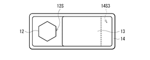
図1は、本開示の一実施の形態に係る発光装置(発光装置1)の断面構成(A)および平面構成(B)の一例を模式的に表したものである。発光装置1は、所謂LEDディスプレイと呼ばれる画像表示装置(例えば、画像表示装置100、図5参照)の表示画素を構成するRGBに対応した各色画素に好適に適用可能なものである。本実施の形態の発光装置1は、例えば、支持基板11の面11S1に、発光素子12と波長変換部13とを並列に配置し、さらに、波長変換部13を間にして支持基板11の面11S1に対して、光反射性を有する傾斜面14S3が配置されている。
<1. Embodiment>
FIG. 1 schematically shows an example of a cross-sectional configuration (A) and a planar configuration (B) of a light emitting device (light emitting device 1) according to an embodiment of the present disclosure. The
(1-1.発光装置の構成)
発光装置1は、上記のように、例えば画像表示装置100の表示画素を構成する、例えばRGBに対応した各色画素(赤色画素R、緑色画素Gおよび青色画素B)を有している。赤色画素R、緑色画素Gおよび青色画素Bには、それぞれ、支持基板11の面11S1に、発光素子12と、RGBに対応する波長変換部13(赤色変換部13R、緑色変換部13Gまたは青色変換部13B)とが設けられている。赤色画素R、緑色画素Gおよび青色画素Bは、例えば隔壁14によって互いに分離されている。隔壁14は、波長変換部13を間にして発光素子12と対向する壁面が、上記光反射性を有する傾斜面14S3となっている。発光素子12の上方には、さらに、遮光部材15が配置されている。以下に、発光装置1の各構成要素について詳細に説明する。
(1-1. Configuration of light emitting device)
As described above, the
支持基板11は、例えば発光素子12の素子駆動回路等が作り込まれたシリコン基板である。
The
発光素子12は、例えばナノコラム型あるいはナノワイヤ型の発光ダイオード(LED)である。図2は、ナノコラム型の発光素子12の断面構成の一例を模式的に表したものである。発光素子12は、例えば、n型結晶構造体12Aと、活性層12Bと、p型半導体層12Cと、n電極12Dと、p電極12Eとを有している。
The
n型結晶構造体12Aは、例えばn型のGaN系の半導体材料により形成されている。n型結晶構造体12Aは、例えば図1および図2に示したように略六角柱状に、支持基板11の面11S1に対して垂直方向(Z軸方向)に立設され、側面の面積が上面の面積よりも大きい形状を有している。 The n-type crystal structure 12A is formed of, for example, an n-type GaN-based semiconductor material. The n-type crystal structure 12A is erected in a substantially hexagonal columnar shape, for example, in a substantially hexagonal columnar shape as shown in FIGS. 1 and 2 in the direction perpendicular to the surface 11S1 of the support substrate 11 (Z-axis direction), and the area of the side surface is the upper surface. It has a shape larger than the area of.
活性層12Bは、例えば、n型結晶構造体12Aの側面および上面に沿って設けられている。活性層12Bは、例えばInGaNとGaNとが交互に積層された多重量子井戸構造を有し、層内に発光領域を有している。活性層12Bは、例えば、発光波長が430nm以上500nm以下の青色領域の光を発する。この他、活性層12Bは、例えば、発光波長が350nm以上430nm以下の紫外領域の光を発するものでもよい。 The active layer 12B is provided, for example, along the side surfaces and the upper surface of the n-type crystal structure 12A. The active layer 12B has, for example, a multiple quantum well structure in which InGaN and GaN are alternately laminated, and has a light emitting region in the layer. The active layer 12B emits light in a blue region having an emission wavelength of 430 nm or more and 500 nm or less, for example. In addition, the active layer 12B may, for example, emit light in the ultraviolet region having an emission wavelength of 350 nm or more and 430 nm or less.
p型半導体層12Cは、活性層12Bの側面および上面に沿って設けられている。p型半導体層12Cは、例えばp型のGaN系半導体材料により形成されている。 The p-type semiconductor layer 12C is provided along the side surface and the upper surface of the active layer 12B. The p-type semiconductor layer 12C is formed of, for example, a p-type GaN-based semiconductor material.
n電極12Dは、複数の発光素子12の各々に独立して設けられており、例えば、支持基板11の面11S1と対向する面側から支持基板11を貫通してn型結晶構造体12Aに接している。n電極12Dは、例えば、ITO(Indiun Tin Oxide)またはIZO(Indiun Zinc Oxide)等の透明電極材料を用いて形成することができる。この他、n電極12Dは、パラジウム(Pd)、チタン(Ti)、アルミニウム(Al)、白金(Pt)、銀(Ag)、ニッケル(Ni)または金(Au)等の金属材料を用いて形成するようにしてもよい。
The
p電極12Eは、p型半導体層12Cの周囲を覆うように設けられている。p電極12Eは、例えば、ITO、IZO、酸化錫(SnO)または酸化チタン(TiO)等の透明電極材料により形成されている。p電極12Eは、例えば複数の発光素子12に対する共通層として設けるようにしてもよい。
The p-electrode 12E is provided so as to cover the periphery of the p-type semiconductor layer 12C. The p-electrode 12E is made of a transparent electrode material such as ITO, IZO, tin oxide (SnO) or titanium oxide (TIO). The p electrode 12E may be provided, for example, as a common layer for a plurality of
p電極12Eの周囲には、さらにパッシベーション膜12Fが設けられている。パッシベーション膜12Fは、発光素子12の表面を保護するためのものである。パッシベーション膜12Fは、例えば、酸化シリコン(SiO)や窒化シリコン(SiN)等により形成されている。パッシベーション膜12Fは、例えば上記のようにp電極12Eが複数の発光素子12に対する共通層として設けられている場合には、p電極12Eと同様に、複数の発光素子12に対する共通層として設けるようにしてもよい。
A passivation film 12F is further provided around the p electrode 12E. The passivation film 12F is for protecting the surface of the
波長変換部13(赤色変換部13R、緑色変換部13Gおよび青色変換部13B)は、赤色画素R、緑色画素Gおよび青色画素Bのそれぞれに設けられた発光素子12から出射された光を所望の波長(例えば、赤色(R)、緑色(G)または青色(B))に変換して出射するためのものである。
The wavelength conversion unit 13 (
赤色変換部13R、緑色変換部13Gおよび青色変換部13Bは、それぞれ、例えばR,G,Bの各色に対応する量子ドットを含んで形成されている。具体的には、赤色光を得る場合には、量子ドットは、例えば、InP、GaInP、InAsP、CdSe、CdZnSe、CdTeSeまたはCdTe等から選択することができる。緑色光を得る場合には、量子ドットは、例えば、InP、GaInP、ZnSeTe、ZnTe、CdSe、CdZnSe、CdSまたはCdSeS等から選択することができる。青色光を得る場合には、ZnSe、ZnTe、ZnSeTe、CdSe、CdZnSe、CdS、CdZnSおよびCdSeS等から選択することができる。上記の中でも、カドミウム(Cd)フリーの材料を用いることが好ましい。
The
量子ドットの変換効率は、入射光強度依存性および温度依存性を有している。概ね、いずれに対しても単純減の傾向を有する。そのため、同じ総光量を量子ドットに入射する場合、光量ムラがあると高強度域の効率が大きく低下し、平均的な入射時よりも総効率が低下する。このため、波長変換部13は、図1に示したように、発光素子12と近接して対向する側面の下部、隔壁14の傾斜面14S3と接する上部および下部がそれぞれ曲面となっていることが好ましい。これにより、単位面積当たりの入射光量が低減され、変換効率の低下が抑制される。このような形状は、例えば、等方エッチングやシャドウマスクリソグラフィ等を用いることで形成することができる。
The conversion efficiency of quantum dots has an incident light intensity dependence and a temperature dependence. In general, there is a tendency for simple decrease in all cases. Therefore, when the same total amount of light is incident on the quantum dots, if there is unevenness in the amount of light, the efficiency in the high-intensity region is greatly reduced, and the total efficiency is lower than that at the time of average incident. Therefore, as shown in FIG. 1, the
なお、発光素子12から青色光が出射される場合には、青色画素Bの青色変換部13Bは、例えば、図3に示したように設けなくてもよい。また、略六角柱状に立設する発光素子12は、例えば成長基板の角度を調整することにより、例えば、図4に示したように、略六角柱状の発光素子12の一の面(例えば、面12S)と、波長変換部13の発光素子12と近接する側面とが正対するように形成してもよい。
When blue light is emitted from the
更に、発光素子12と波長変換部13との間は空気層でもよいし、あるいは、光透過性を有するSiO膜や樹脂層によって埋設されていてもよい。樹脂層によって埋設する場合には、樹脂層には、例えば酸化チタン(TiO2)等のナノパーティクルを散乱材として分散させるようにしてもよい。
Further, the space between the light emitting
隔壁14は、赤色画素R、緑色画素Gおよび青色画素Bを区画すると共に、隣接する色画素間の混色を防ぐためのものである。隔壁14は、赤色画素R、緑色画素Gおよび青色画素B毎に、内側に例えば略矩形状の空間を形成しており、この内側の空間に、発光素子12および波長変換部13(赤色変換部13R、緑色変換部13Gまたは青色変換部13B)が設けられている。隔壁14の内側の空間を構成する4つの壁面のうち、波長変換部13を間にして発光素子12と対向する1つの壁面は、隔壁14の底面14S2とのなす角が90°未満となる傾斜面14S3となっている。この傾斜面14S3が、本開示の「光反射面」の一具体例に相当し、傾斜面14S3が形成されている隔壁14部分が、本開示の「光反射部材」の一具体例に相当する。その他の壁面は、支持基板11の面11S1に対して略垂直に立設されている。
The
隔壁14は、例えばアルミニウム(Al)、銀(Ag)およびロジウム(Rh)等の光反射性を有する金属材料を用いて形成されている。この他、隔壁14は、例えばシリコン基板をエッチングして図1に示した隔壁14の形状とし、その表面にAl等の金属膜をコーティングすることで形成するようにしてもよい。これにより、大口径シリコン工程との相性よく、隔壁14を形成することができる。
The
遮光部材15は、発光素子12から出射された0次光が発光装置1から取り出されるのを防ぐためのものであり、発光素子12の上方に配置されている。遮光部材15は、例えば隔壁14の上面14S1によって支持されており、波長変換部13の一部まで延在している。遮光部材15は、遮光性と共に、例えば隔壁14と同様に光反射性を有していることが好ましく、例えばAl、AgおよびRh等の金属材料を用いて形成することができる。これにより、発光素子12から上方に出射された光が遮光部材15によって反射されるようになり、発光素子12から出射された光の導光効率が向上する。この遮光部材15が、本開示の「光反射膜」の一具体例に相当する。
The light-shielding
なお、遮光部材15の下面(発光素子12との対向面)に光反射膜を設けることでも同様の効果を得ることができる。この他、遮光部材15は、例えば発光素子12から出射される波長の光を選択的に反射するダイクロイックミラーを用いて形成するようにしてもよい。
The same effect can be obtained by providing a light reflecting film on the lower surface of the light shielding member 15 (the surface facing the light emitting element 12). In addition, the light-shielding
上記のような構成により、発光素子12から出射された光Lは、図1(A),(B)に示したように、直接または隔壁14の壁面に反射されて波長変換部13に入射し、所望の波長に変換された後、遮光部材15が形成されていない波長変換部13の上面から出射される。
With the above configuration, the light L emitted from the
(1-2.画像表示装置の構成)
図5は、本開示の画像表示装置(画像表示装置100)の概略構成の一例を表した斜視図である。画像表示装置100は、所謂LEDディスプレイと呼ばれるものであり、表示画素に本実施の形態の発光装置1を用いたものである。画像表示装置100は、例えば図5に示したように、表示パネル110と、表示パネル110を駆動する制御回路140とを備えている。
(1-2. Configuration of image display device)
FIG. 5 is a perspective view showing an example of a schematic configuration of the image display device (image display device 100) of the present disclosure. The image display device 100 is a so-called LED display, and the
表示パネル110は、実装基板120と、対向基板130とを互いに重ね合わせたものである。対向基板130の表面が映像表示面となっており、中央部分に表示領域100Aを有し、その周囲に、非表示領域であるフレーム領域100Bを有している。
The
図6は、実装基板120の対向基板130側の表面のうち、表示領域100Aに対応する領域の配線レイアウトの一例を表したものである。実装基板120の表面のうち表示領域100Aに対応する領域には、例えば図6に示したように、複数のデータ配線121が所定の方向に延在して形成されており、かつ所定のピッチで並列配置されている。実装基板120の表面のうち表示領域100Aに対応する領域には、さらに、例えば、複数のスキャン配線122がデータ配線121と交差(例えば、直交)する方向に延在して形成されており、且つ、所定のピッチで並列配置されている。データ配線121およびスキャン配線122は、例えば、Cu(銅)等の導電性材料からなる。
FIG. 6 shows an example of the wiring layout of the area corresponding to the
スキャン配線122は、例えば、最表層に形成されており、例えば、基材表面に形成された絶縁層(図示せず)上に形成されている。なお、実装基板120の基材は、例えば、シリコン基板、または樹脂基板等からなり、基材上の絶縁層は、例えば、窒化シリコン(SiN)、酸化シリコン(SiO)、酸化アルミニウム(AlO)または樹脂材料からなる。一方、データ配線121は、スキャン配線122を含む最表層とは異なる層(例えば、最表層よりも下の層)内に形成されており、例えば、基材上の絶縁層内に形成されている。
The scan wiring 122 is formed, for example, on the outermost layer, for example, on an insulating layer (not shown) formed on the surface of the base material. The substrate of the mounting
データ配線121とスキャン配線122との交差部分の近傍が表示画素123となっており、複数の表示画素123が表示領域100A内においてマトリクス状に配置されている。各表示画素123には、例えば、RGBに対応する色画素(赤色画素R、緑色画素Gおよび青色画素B)を有する発光装置1が実装されている。なお、図6には、3つの色画素(赤色画素R、緑色画素Gおよび青色画素B)で一つの表示画素123が構成されており、赤色画素Rから赤色の光を、緑色画素Gから緑色の光を、青色画素Bから青色の光をそれぞれ出力することができるようになっている場合が例示されている。
A
発光装置1には、例えば赤色画素R、緑色画素Gおよび青色画素B毎に一対、または一方が共通且つ他方が赤色画素R、緑色画素Gおよび青色画素B毎に配置される端子電極が設けられている。そして、一方の端子電極がデータ配線121に電気的に接続されており、他方の端子電極がスキャン配線122に電気的に接続されている。例えば、一方の端子電極は、データ配線121に設けられた分枝121Aの先端のパッド電極121Bに電気的に接続されている。また、例えば、他方の端子電極は、スキャン配線122に設けられた分枝122Aの先端のパッド電極122Bに電気的に接続されている。
The
各パッド電極121B,122Bは、例えば、最表層に形成されており、例えば、図6に示したように、各発光装置1が実装される部位に設けられている。ここで、パッド電極121B,122Bは、例えば、Au(金)等の導電性材料からなる。
The
実装基板120には、さらに、例えば、実装基板120と対向基板130との間の間隔を規制する複数の支柱(図示せず)が設けられている。支柱は、表示領域100Aとの対向領域内に設けられていてもよいし、フレーム領域100Bとの対向領域内に設けられていてもよい。
The mounting
対向基板130は、例えば、ガラス基板、または樹脂基板等からなる。対向基板130において、発光装置1側の表面は平坦となっていてもよいが、粗面となっていることが好ましい。粗面は、表示領域100Aとの対向領域全体に渡って設けられていてもよいし、表示画素123との対向領域にだけ設けられていてもよい。粗面は、赤色画素R、緑色画素Gおよび青色画素Bから発せられた光が当該粗面に入細かな凹凸を有している。粗面の凹凸は、例えば、サンドブラストや、ドライエッチング等によって作製可能である。
The facing substrate 130 is made of, for example, a glass substrate, a resin substrate, or the like. In the facing substrate 130, the surface on the
制御回路140は、映像信号に基づいて各表示画素123(各発光装置1)を駆動するものである。制御回路140は、例えば、表示画素123に接続されたデータ配線121を駆動するデータドライバと、表示画素123に接続されたスキャン配線122を駆動するスキャンドライバとにより構成されている。制御回路140は、例えば、図5に示したように、表示パネル110とは別体で設けられ、且つ配線を介して実装基板120と接続されていてもよいし、実装基板120上に実装されていてもよい。
The control circuit 140 drives each display pixel 123 (each light emitting device 1) based on a video signal. The control circuit 140 is composed of, for example, a data driver for driving the data wiring 121 connected to the
(1-3.作用・効果)
本実施の形態の発光装置1では、支持基板11の面11S1に、発光素子12と波長変換部13とを並列に配置し、さらに、波長変換部13を間にして支持基板11の面11S1に対して、光反射性を有する傾斜面14S3を配置するようにした。これにより、発光素子12から出射され、波長変換部13を通過する光の光路長が確保される。以下、これについて説明する。
(1-3. Action / effect)
In the
所謂マイクロLEDを光源として用いた画像表示装置では、前述したように、各マイクロLEDの上方に、例えば量子ドットを含む波長変換層を配置し、この波長変換層を通過することで所望の波長に変換された光をRGBの各色光として取り出す画像表示素子が用いられている。 In an image display device using a so-called micro LED as a light source, as described above, a wavelength conversion layer containing, for example, a quantum dot is arranged above each micro LED, and the wavelength conversion layer is passed through the wavelength conversion layer to obtain a desired wavelength. An image display element that extracts the converted light as each color light of RGB is used.
ところが、このような構造を有する画像表示素子では、一般に、マイクロLEDから出射された光(励起光)を波長変換層において高効率に波長変換することが難しく、色ずれ、輝度の低下および発熱等の問題を生じる。因みに、色ずれは、例えば、励起光としてマイクロLEDから出射される、例えば青色光が波長変換層で変換されずに漏れ出ることによるものである、また、赤色および緑色にそれぞれ対応する量子ドットの波長変換効率の低さに起因する赤色光成分および緑色光成分の不足によるものである。輝度の低下は、波長変換効率およびそれに伴う光取り出し効率の異なる色画素間でのホワイトバランスの調整や視感度等によるものである。発熱は、ホワイトバランスを調整するために不要となる、例えば青色光成分を処理することによるものである。 However, in an image display element having such a structure, it is generally difficult to efficiently convert the wavelength of the light (excitation light) emitted from the micro LED in the wavelength conversion layer, such as color shift, decrease in brightness, and heat generation. Causes the problem of. Incidentally, the color shift is caused by, for example, leakage of blue light emitted from the micro LED as excitation light without being converted by the wavelength conversion layer, and of quantum dots corresponding to red and green, respectively. This is due to the lack of red light component and green light component due to the low wavelength conversion efficiency. The decrease in luminance is due to adjustment of white balance between color pixels having different wavelength conversion efficiencies and associated light extraction efficiencies, visual sensitivity, and the like. The heat generation is due to processing, for example, a blue light component, which is unnecessary for adjusting the white balance.
この問題は、例えば波長変換層の厚膜を厚くして変換効率に寄与する光路長を確保することで解決することができる。しかしながら、波長変換層の厚膜化は、波長変換層の形成工程の難易度の上昇や、隣接する波長変換層の間を分離する画素分離壁のアスペクト比の増加による加工難易度の上昇といった課題を生じる。また、波長変換層の厚膜化は、表示画素の微細化に対して不利となる。これらの課題は、マイクロLEDを用いる自発光型のマイクロディスプレイにおいて特に重要となる。 This problem can be solved, for example, by thickening the thick film of the wavelength conversion layer to secure the optical path length that contributes to the conversion efficiency. However, thickening the wavelength conversion layer has problems such as an increase in the difficulty of the process of forming the wavelength conversion layer and an increase in the processing difficulty due to an increase in the aspect ratio of the pixel separation wall that separates the adjacent wavelength conversion layers. Produces. Further, thickening the wavelength conversion layer is disadvantageous for miniaturization of display pixels. These issues are particularly important in self-luminous micro-displays that use micro LEDs.
これに対して、本実施の形態の発光装置1では、発光素子12と波長変換部13とを並列に配置し、波長変換部13の背面(発光素子12と対向する側面と対向する面)側に光反射性を有する傾斜面14S3を設けることで、発光素子12から出射され、波長変換部13において波長変換された光を発光装置1から取り出すようにした。これにより、波長変換部13を通過する、発光素子12から出射された光(励起光)の光路長を確保することが可能となる。
On the other hand, in the
以上により、本実施の形態の発光装置1では、発光素子12の上方に波長変換層を配置した場合と比較して、発光素子12から出射された光(励起光)の、波長変換部13を通過する光路長を十分かつ容易に確保することができ、波長変換部13における波長変換効率を向上させることが可能となる。
As described above, in the
また、本実施の形態の発光装置1では、発光素子12と波長変換部13とを並列に配置するようにしたので、発光装置1を低背化することが可能となる。
Further, in the
特に、本実施の発光装置1は、自発光型のマイクロディスプレイの表示画素として適用することにより、色ずれ、輝度の低下および発熱等が改善された、優れた表示品位を有するマイクロディスプレイを実現することができる。
In particular, the
次に、本開示の変形例(変形例1~8)について説明する。以下では、上記実施の形態と同様の構成要素については同一の符号を付し、適宜その説明を省略する。 Next, modification examples (modification examples 1 to 8) of the present disclosure will be described. In the following, the same components as those in the above embodiment are designated by the same reference numerals, and the description thereof will be omitted as appropriate.
<2.変形例1>
図7は、本開示の変形例1に係る発光装置(発光装置1A)の断面構成(A)および平面構成(B)の一例を模式的に表したものである。本変形例の発光装置1Aでは、例えば略矩形形状を有する隔壁14の内側の空間の、例えば中央に発光素子12を配置し、発光素子12を間にした両側に波長変換部13および光反射性を有する傾斜面14S3を設けた点が、上記実施の形態とは異なる。
<2.
FIG. 7 schematically shows an example of the cross-sectional configuration (A) and the planar configuration (B) of the light emitting device (light emitting device 1A) according to the modified example 1 of the present disclosure. In the light emitting device 1A of this modification, for example, the
このように、本変形例では、発光素子12の両側に波長変換部13および傾斜面14S3を設けるようにしたので、発光素子12から出射された光(励起光)が波長変換部13に入射するまでの、隔壁14の壁面において反射される反射回数を低減することが可能となる。よって、上記実施の形態と比較して、発光素子12から出射された光の利用効率を向上させることが可能となる。
As described above, in this modification, since the
<3.変形例2>
図8は、本開示の変形例2に係る発光装置(発光装置1B)の断面構成の一例を模式的に表したものである。上記実施の形態等では、発光素子12としてナノコラム型あるいはナノワイヤ型の発光ダイオード(LED)を用いた例を示したが、発光素子12は、例えば、図8に示したように、例えば支持基板11の面11S1に対して平行な一面にのみ活性層を有するプレーナ型のLEDを用いた場合においても本技術は有効であり、上記実施の形態と同様の効果を得ることができる。
<3. Modification 2>
FIG. 8 schematically shows an example of the cross-sectional configuration of the light emitting device (light emitting device 1B) according to the second modification of the present disclosure. In the above embodiment and the like, an example in which a nanocolumn type or nanowire type light emitting diode (LED) is used as the
<4.変形例3>
図9および図10は、本開示の変形例3に係る発光装置(発光装置1C)の平面構成の一例を模式的に表したものである。上記実施の形態では、隣接する赤色画素R、緑色画素Gおよび青色画素Bの間を分離する、隔壁14の対向する壁面14S4が略平行な例を示したが、これに限らない。
<4.
9 and 10 schematically show an example of the planar configuration of the light emitting device (light emitting device 1C) according to the third modification of the present disclosure. In the above embodiment, an example is shown in which the facing wall surfaces 14S4 of the
例えば、隔壁14の壁面14S4は、図9に示したように、平面視において略台形形状となるように、例えば発光素子12が配置された側から傾斜面14S3側に向かって対向する壁面14S4の幅が徐々に広がるようにしてもよい。また、上記変形例1において説明したように、発光素子12を間にした両側に波長変換部13および傾斜面14S3を設ける場合には、図10に示したように、平面視において略六角形状となるように、例えば、発光素子12が配置された壁面14C4の中央から傾斜面14S3側に向かって対向する壁面14S4の幅が徐々に狭まるようにしてもよい。
For example, as shown in FIG. 9, the wall surface 14S4 of the
このように、隔壁14の対向する壁面14S4に角度をつけることにより、壁面14S4において反射された光が波長変換部13へ効率よく反射されるようになる。よって、上記実施の形態等の効果に加えて、発光素子12から出射された光の利用効率をさらに向上させることが可能となる。
By angling the facing wall surface 14S4 of the
<5.変形例4>
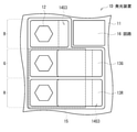
図11は、本開示の変形例4に係る発光装置(発光装置1D)の平面構成の一例を模式的に表したものである。上記実施の形態では、赤色画素R、緑色画素Gおよび青色画素Bが互いに略同じ面積を有する例を示したが、これに限らない。例えば、赤色画素R、緑色画素Gおよび青色画素Bの各面積は、各波長変換部13(赤色変換部13R、緑色変換部13Gおよび青色変換部13B)の波長変換効率に応じた面積としてもよい。
<5. Modification 4>
FIG. 11 schematically shows an example of the planar configuration of the light emitting device (light emitting
具体的には、上記のように、青色光を出射する発光素子12を用いる場合には、青色画素Bでは発光素子12から出射された光をそのまま用いることができるため、青色変換部13Bを省略することができる。その場合には、例えば、図11に示したように、青色画素Bの面積を、赤色画素Rおよび緑色画素Gよりも小さくすることができ、空いたスペースには、例えば回路16等を設けることができる。
Specifically, as described above, when the
また、一般に緑色に対応する量子ドットは、赤色に対応する量子ドットよりも波長変換効率が低い。そのため、例えば、図12に示したように、青色画素Bの削減されたスペースに、緑色画素Gを延在させ、緑色変換部13G内を通過する光の光路長を稼ぐようにしてもよい。これにより、緑色画素Gにおける波長変換効率を向上させることが可能となる。よって、赤色画素R、緑色画素Gおよび青色画素Bにおける光の利用効率が向上し、輝度を向上させることが可能となる。
Further, in general, the quantum dots corresponding to green have a lower wavelength conversion efficiency than the quantum dots corresponding to red. Therefore, for example, as shown in FIG. 12, the green pixel G may be extended in the reduced space of the blue pixel B to increase the optical path length of the light passing through the
<6.変形例5>
図13は、本開示の変形例5に係る発光装置(発光装置1E)の平面構成の一例を模式的に表したものである。本変形例では、例えばナノコラム型の発光素子12の外周全体にわたって波長変換部13を設けた点が、上記実施の形態とは異なる。
<6. Modification 5>
FIG. 13 schematically shows an example of the planar configuration of the light emitting device (light emitting device 1E) according to the modified example 5 of the present disclosure. In this modification, for example, the
このように、発光素子12の外周全体にわたって波長変換部13を設けることにより、波長変換部13内を通過する光の光路長をさらに確保することができる。これにより、上記実施の形態と比較して、波長変換効率をさらに向上させることが可能となる。
By providing the
<7.変形例6>
図14は、本開示の変形例6に係る発光装置(発光装置1F)の断面構成の一例を模式的に表したものである。本変形例では、波長変換部13の底面および傾斜面14S3と接する側面にわたって熱引き部17を設けた点が、上記実施の形態とは異なる。
<7. Modification 6>
FIG. 14 schematically shows an example of the cross-sectional configuration of the light emitting device (light emitting
熱引き部17は、波長変換時に発生した熱を放熱し、波長変換部13の温度上昇を低減するためのものである。熱引き部17は、傾斜面14S3における光反射性を確保するために、例えばAl等の光反射性を有する金属膜によって形成することが好ましい。この熱引き部17が、本開示の「放熱部材」の一具体例に相当する。
The heat drawing unit 17 is for dissipating heat generated during wavelength conversion and reducing the temperature rise of the
このように、本変形例では、波長変換部13の底面および傾斜面14S3と接する側面にわたって熱引き部17を設けるようにしたので、波長変換時に発生した熱による波長変換部13の温度上昇が低減され、波長変換部13を構成する量子ドットの波長変換効率の低下を抑制することができる。よって、上記実施の形態と比較して、波長変換効率をさらに向上させることが可能となる。
As described above, in this modification, since the heat drawing portion 17 is provided over the bottom surface of the
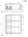
<8.変形例7>
図15は、本開示の変形例7に係る発光装置(発光装置1G)の断面構成(A)および平面構成(B)の一例を模式的に表したものである。本変形例では、赤色画素R、緑色画素Gおよび青色画素B毎に複数(ここでは4つ)の発光素子12を設けた点が、上記実施の形態とは異なる。
<8. Modification 7>
FIG. 15 schematically shows an example of the cross-sectional configuration (A) and the planar configuration (B) of the light emitting device (light emitting device 1G) according to the modified example 7 of the present disclosure. In this modification, a plurality of (here, four)
なお、図15では、4つの発光素子12を2行2列に配置した例を示したが、複数の発光素子12の配置例はこれに限らない。例えば、図16に示したように、例えば3つの発光素子12を互いに違いに配置するようにしてもよい。
Although FIG. 15 shows an example in which the four
このように、各色画素(赤色画素R、緑色画素Gおよび青色画素B)には、複数の発光素子12を設けるようにしてもよい。これにより、1つの発光素子12を設けた場合と比較して、さらに発光装置1の低背化を図ることが可能となる。また、1つの発光素子12を設けた場合と比較して、波長変換部13への入射光線が均質化されるため、波長変換効率をさらに向上させることが可能となる。加えて、波長変換部13における発熱を低減することが可能となる。
In this way, each color pixel (red pixel R, green pixel G, and blue pixel B) may be provided with a plurality of
<9.変形例8>
図17は、本開示の発光装置(例えば、発光装置1)を用いた画像表示装置の他の構成例(画像表示装置200)を表した斜視図である。画像表示装置200は、LEDを光源として用いた、所謂タイリングディスプレイと呼ばれるものであり、表示画素として本実施の形態の発光装置1が用いられたものである。画像表示装置200は、例えば、図17に示したように、表示パネル210と、表示パネル210を駆動する制御回路240とを備えている。
<9. Modification 8>
FIG. 17 is a perspective view showing another configuration example (image display device 200) of the image display device using the light emitting device (for example, the light emitting device 1) of the present disclosure. The image display device 200 is a so-called tiling display using an LED as a light source, and the
表示パネル210は、実装基板220と、対向基板230とを互いに重ね合わせたものである。対向基板230の表面が映像表示面となっており、中央部分に表示領域を有し、その周囲に、非表示領域であるフレーム領域を有している(いずれも図示せず)。対向基板230は、例えば、所定の間隙を介して、実装基板220と対向する位置に配置されている。なお、対向基板230が、実装基板220の上面に接していてもよい。
The
図18は、実装基板220の構成の一例を模式的に表したものである。実装基板220は、例えば、図18に示したように、タイル状に敷き詰められた複数のユニット基板250により構成されている。なお、図18では、9つのユニット基板250により実装基板220が構成される例を示したが、ユニット基板250の数は、10以上であってもよいし、8以下であってもよい。
FIG. 18 schematically shows an example of the configuration of the mounting
図19は、ユニット基板250の構成の一例を表したものである。ユニット基板250は、例えば、タイル状に敷き詰められた複数の赤色画素R、緑色画素Gおよび青色画素Bを有する発光装置1と、各発光装置1を支持する支持基板260とを有している。各ユニット基板250は、さらに、制御基板(図示せず)を有している。支持基板260は、例えば、金属フレーム(金属板)、もしくは、配線基板等で構成されている。支持基板260が配線基板で構成されている場合には、制御基板を兼ねることも可能である。このとき、支持基板260および制御基板の少なくとも一方が、各発光装置1と電気的に接続されている。
FIG. 19 shows an example of the configuration of the
以上、実施の形態および変形例1~8を挙げて本開示を説明したが、本開示は上記実施の形態に限定されるものではなく、種々変形可能である。例えば、上記実施の形態等において例示した発光素子12の構成要素、配置および数等は、あくまで一例であり、全ての構成要素を備える必要はなく、また、他の構成要素をさらに備えていてもよい。
Although the present disclosure has been described above with reference to embodiments and
また、上述した変形例1~8は、それぞれの構成を互いに組み合わせることができる。例えば、変形例1,3~7では、ナノコラム型の発光素子12を用いた例を示したが、変形例2に示したようなプレーナ型の発光素子12を用いた場合にも同様の効果を得ることができる。
Further, in the above-mentioned
更に、上記実施の形態等では、発光装置1等を画像表示装置100,200等に適用した例を示したが、本開示の発光装置1等は、照明装置として用いることもできる。
Further, in the above-described embodiment and the like, an example in which the
なお、本明細書に記載された効果はあくまで例示であってこれに限定されるものではなく、また他の効果があってもよい。 It should be noted that the effects described in the present specification are merely examples and are not limited thereto, and other effects may be obtained.
本技術は以下のような構成を取ることも可能である。以下の構成の本技術によれば、発光素子と波長変換部とを並列に配置し、さらに、波長変換部を間にして、傾斜した光反射面を構成する光反射部材を発光素子と対向配置するようにした。これにより、発光素子から出射され、波長変換部を通過する光の光路長が確保される。よって、波長変換効率を向上させることが可能となる。
(1)
一の面を有する支持部材と、
前記支持部材の前記一の面に設けられた発光素子と、
前記支持部材の前記一の面に、前記発光素子と並列に配置された波長変換部と、
前記波長変換部を間にして前記発光素子と対向配置されると共に、前記支持部材の前記一の面に対して傾斜した光反射面を形成する光反射部材と
を備えた発光装置。
(2)
前記発光素子の上方に光反射膜をさらに有する、前記(1)に記載の発光装置。
(3)
前記光反射膜は、前記発光素子の上方から前記波長変換部の一部まで延在している、前記(2)に記載の発光装置。
(4)
前記波長変換部および前記光反射部材は、それぞれ、前記発光素子を間にして両側に配置されている、前記(1)乃至(3)のうちのいずれか1つに記載の発光装置。
(5)
前記支持部材の前記一の面に配置され、前記発光素子の周囲を囲む隔壁をさらに有する、前記(1)乃至(4)のうちのいずれか1つに記載の発光装置。
(6)
前記隔壁の壁面の少なくとも一部が、前記光反射部材を構成している、前記(5)に記載の発光装置。
(7)
前記支持部材の前記一の面に、前記発光素子が複数設けられており、
前記複数の発光素子のそれぞれは、前記隔壁によって分離されている、前記(5)または(6)に記載の発光装置。
(8)
前記複数の発光素子の間に設けられた前記隔壁の壁面は、前記支持部材の前記一の面に対して垂直に設けられている、前記(7)に記載の発光装置。
(9)
赤色、緑色および青色に対応する複数の色画素を有し、
前記発光素子は、前記複数の色画素毎に設けられている、前記(1)乃至(8)のうちのいずれか1つに記載の発光装置。
(10)
前記赤色に対応する色画素および前記緑色に対応する色画素では、それぞれ、前記波長変換部を介して出射された赤色光および緑色光を取り出し、
前記青色に対応する色画素では、前記発光素子から出射された光を、前記波長変換部を介さずに青色光として直接取り出す、前記(9)に記載の発光装置。
(11)
前記波長変換部は、平面視において、前記発光素子の外周全体にわたって設けられている、前記(1)乃至(10)のうちのいずれか1つに記載の発光装置。
(12)
前記波長変換部と前記支持部材との間におよび前記波長変換部と前記光反射部材との間には、放熱部材がさらに設けられている、前記(1)乃至(11)のうちのいずれか1つに記載の発光装置。
(13)
前記発光素子は、ナノコラム構造またはナノワイヤ構造を有する発光ダイオードである、前記(1)乃至(12)のうちのいずれか1つに記載の発光装置。
(14)
前記波長変換部は、量子ドットを含んで形成されている、前記(1)乃至(13)のうちのいずれか1つに記載の発光装置。
(15)
前記量子ドットは、カドミウムフリー量子ドットである、前記(14)に記載の発光装置。
(16)
前記光反射膜は、金属膜またはダイクロイックミラーを用いて形成されている、前記(2)乃至(15)のうちのいずれか1つに記載の発光装置。
(17)
1または複数の発光装置を備え、
前記発光装置は、
一の面を有する支持部材と、
前記支持部材の前記一の面に設けられた発光素子と、
前記支持部材の前記一の面に、前記発光素子と並列に配置された波長変換部と、
前記波長変換部を間にして前記発光素子と対向配置されると共に、前記支持部材の前記一の面に対して傾斜した光反射面を形成する光反射部材と
を有する画像表示装置。
The present technology can also have the following configurations. According to the present technology having the following configuration, the light emitting element and the wavelength conversion unit are arranged in parallel, and the light reflecting member constituting the inclined light reflecting surface is arranged facing the light emitting element with the wavelength conversion unit in between. I tried to do it. As a result, the optical path length of the light emitted from the light emitting element and passing through the wavelength conversion unit is secured. Therefore, it is possible to improve the wavelength conversion efficiency.
(1)
A support member with one surface and
A light emitting element provided on the one surface of the support member and
A wavelength conversion unit arranged in parallel with the light emitting element on the one surface of the support member,
A light emitting device including a light reflecting member which is arranged to face the light emitting element with the wavelength conversion unit in between and forms a light reflecting surface inclined with respect to the one surface of the support member.
(2)
The light emitting device according to (1) above, further comprising a light reflecting film above the light emitting element.
(3)
The light emitting device according to (2) above, wherein the light reflecting film extends from above the light emitting element to a part of the wavelength conversion unit.
(4)
The light emitting device according to any one of (1) to (3), wherein the wavelength conversion unit and the light reflecting member are arranged on both sides of the light emitting element, respectively.
(5)
The light emitting device according to any one of (1) to (4) above, which is arranged on the one surface of the support member and further has a partition wall surrounding the light emitting element.
(6)
The light emitting device according to (5) above, wherein at least a part of the wall surface of the partition wall constitutes the light reflecting member.
(7)
A plurality of the light emitting elements are provided on the one surface of the support member.
The light emitting device according to (5) or (6) above, wherein each of the plurality of light emitting elements is separated by the partition wall.
(8)
The light emitting device according to (7), wherein the wall surface of the partition wall provided between the plurality of light emitting elements is provided perpendicular to the one surface of the support member.
(9)
Has multiple color pixels corresponding to red, green and blue,
The light emitting device according to any one of (1) to (8), wherein the light emitting element is provided for each of the plurality of color pixels.
(10)
In the color pixel corresponding to the red color and the color pixel corresponding to the green color, the red light and the green light emitted through the wavelength conversion unit are taken out, respectively.
The light emitting device according to (9) above, wherein the color pixel corresponding to the blue color directly extracts the light emitted from the light emitting element as blue light without going through the wavelength conversion unit.
(11)
The light emitting device according to any one of (1) to (10), wherein the wavelength conversion unit is provided over the entire outer circumference of the light emitting element in a plan view.
(12)
Any of the above (1) to (11), in which a heat radiating member is further provided between the wavelength conversion unit and the support member and between the wavelength conversion unit and the light reflection member. The light emitting device according to one.
(13)
The light emitting device according to any one of (1) to (12) above, wherein the light emitting element is a light emitting diode having a nanocolumn structure or a nanowire structure.
(14)
The light emitting device according to any one of (1) to (13) above, wherein the wavelength conversion unit is formed to include quantum dots.
(15)
The light emitting device according to (14) above, wherein the quantum dots are cadmium-free quantum dots.
(16)
The light emitting device according to any one of (2) to (15) above, wherein the light reflecting film is formed by using a metal film or a dichroic mirror.
(17)
Equipped with one or more light emitting devices,
The light emitting device is
A support member with one surface and
A light emitting element provided on the one surface of the support member and
A wavelength conversion unit arranged in parallel with the light emitting element on the one surface of the support member,
An image display device having a light-reflecting member arranged opposite to the light-emitting element with the wavelength conversion unit in between and forming a light-reflecting surface inclined with respect to the one surface of the support member.
1,1A,1B,1C,1D,1E,1F,1G…発光装置、11…支持基板、12…発光素子、12A…n型結晶構造体、12B…活性層、12C…p型半導体層、12D…n電極、12E…p電極、12F…パッシベーション膜、13…波長変換部、13R…赤色変換部、13G…緑色変換部、14…隔壁、14S1…上面、14S2…底面、14S3…傾斜面、14S4…壁面、15…遮光部材、16…回路、17…熱引き部、100,200…画像表示装置。 1,1A, 1B, 1C, 1D, 1E, 1F, 1G ... light emitting device, 11 ... support substrate, 12 ... light emitting element, 12A ... n-type crystal structure, 12B ... active layer, 12C ... p-type semiconductor layer, 12D ... n electrode, 12E ... p electrode, 12F ... passion film, 13 ... wavelength conversion unit, 13R ... red conversion unit, 13G ... green conversion unit, 14 ... partition wall, 14S1 ... top surface, 14S2 ... bottom surface, 14S3 ... inclined surface, 14S4 ... wall surface, 15 ... shading member, 16 ... circuit, 17 ... heat drawing part, 100, 200 ... image display device.
Claims (17)
前記支持部材の前記一の面に設けられた発光素子と、
前記支持部材の前記一の面に、前記発光素子と並列に配置された波長変換部と、
前記波長変換部を間にして前記発光素子と対向配置されると共に、前記支持部材の前記一の面に対して傾斜した光反射面を形成する光反射部材と
を備えた発光装置。 A support member with one surface and
A light emitting element provided on the one surface of the support member and
A wavelength conversion unit arranged in parallel with the light emitting element on the one surface of the support member,
A light emitting device including a light reflecting member which is arranged to face the light emitting element with the wavelength conversion unit in between and forms a light reflecting surface inclined with respect to the one surface of the support member.
前記複数の発光素子のそれぞれは、前記隔壁によって分離されている、請求項5に記載の発光装置。 A plurality of the light emitting elements are provided on the one surface of the support member.
The light emitting device according to claim 5, wherein each of the plurality of light emitting elements is separated by the partition wall.
前記発光素子は、前記複数の色画素毎に設けられている、請求項1に記載の発光装置。 Has multiple color pixels corresponding to red, green and blue,
The light emitting device according to claim 1, wherein the light emitting element is provided for each of the plurality of color pixels.
前記青色に対応する色画素では、前記発光素子から出射された光を前記波長変換部を介さずに青色光として直接取り出す、請求項9に記載の発光装置。 In the color pixel corresponding to the red color and the color pixel corresponding to the green color, the red light and the green light emitted through the wavelength conversion unit are taken out, respectively.
The light emitting device according to claim 9, wherein in the color pixel corresponding to the blue color, the light emitted from the light emitting element is directly taken out as blue light without going through the wavelength conversion unit.
前記発光装置は、
一の面を有する支持部材と、
前記支持部材の前記一の面に設けられた発光素子と、
前記支持部材の前記一の面に、前記発光素子と並列に配置された波長変換部と、
前記波長変換部を間にして前記発光素子と対向配置されると共に、前記支持部材の前記一の面に対して傾斜した光反射面を形成する光反射部材と
を有する画像表示装置。 Equipped with one or more light emitting devices,
The light emitting device is
A support member with one surface and
A light emitting element provided on the one surface of the support member and
A wavelength conversion unit arranged in parallel with the light emitting element on the one surface of the support member,
An image display device having a light-reflecting member arranged opposite to the light-emitting element with the wavelength conversion unit in between and forming a light-reflecting surface inclined with respect to the one surface of the support member.
Priority Applications (5)
| Application Number | Priority Date | Filing Date | Title |
|---|---|---|---|
| JP2020123307A JP2022019455A (en) | 2020-07-17 | 2020-07-17 | Light-emitting device and image display device |
| CN202180049251.7A CN115803900A (en) | 2020-07-17 | 2021-07-06 | Light emitting device and image display apparatus |
| PCT/JP2021/025525 WO2022014421A1 (en) | 2020-07-17 | 2021-07-06 | Light-emitting device and image display device |
| EP21842283.0A EP4184599A4 (en) | 2020-07-17 | 2021-07-06 | Light-emitting device and image display device |
| US18/004,903 US20230361256A1 (en) | 2020-07-17 | 2021-07-06 | Light-emitting device and image display apparatus |
Applications Claiming Priority (1)
| Application Number | Priority Date | Filing Date | Title |
|---|---|---|---|
| JP2020123307A JP2022019455A (en) | 2020-07-17 | 2020-07-17 | Light-emitting device and image display device |
Publications (1)
| Publication Number | Publication Date |
|---|---|
| JP2022019455A true JP2022019455A (en) | 2022-01-27 |
Family
ID=79554770
Family Applications (1)
| Application Number | Title | Priority Date | Filing Date |
|---|---|---|---|
| JP2020123307A Pending JP2022019455A (en) | 2020-07-17 | 2020-07-17 | Light-emitting device and image display device |
Country Status (5)
| Country | Link |
|---|---|
| US (1) | US20230361256A1 (en) |
| EP (1) | EP4184599A4 (en) |
| JP (1) | JP2022019455A (en) |
| CN (1) | CN115803900A (en) |
| WO (1) | WO2022014421A1 (en) |
Cited By (2)
| Publication number | Priority date | Publication date | Assignee | Title |
|---|---|---|---|---|
| WO2023189384A1 (en) * | 2022-03-31 | 2023-10-05 | ソニーグループ株式会社 | Light-emitting device and image display device |
| WO2023234066A1 (en) * | 2022-05-30 | 2023-12-07 | キヤノン株式会社 | Display element and display device |
Family Cites Families (15)
| Publication number | Priority date | Publication date | Assignee | Title |
|---|---|---|---|---|
| JP5786278B2 (en) * | 2010-04-07 | 2015-09-30 | 日亜化学工業株式会社 | Light emitting device |
| JP2013037139A (en) * | 2011-08-05 | 2013-02-21 | Panasonic Corp | Self-luminous display device |
| US9111464B2 (en) * | 2013-06-18 | 2015-08-18 | LuxVue Technology Corporation | LED display with wavelength conversion layer |
| JP2015195170A (en) * | 2014-03-24 | 2015-11-05 | 三菱化学株式会社 | Spot lighting device |
| JP6357349B2 (en) * | 2014-05-16 | 2018-07-11 | 株式会社ジャパンディスプレイ | Display device |
| KR102222580B1 (en) * | 2014-07-30 | 2021-03-05 | 삼성전자주식회사 | Light emitting device package and display device including the same |
| US9620686B2 (en) * | 2015-01-28 | 2017-04-11 | Apple Inc. | Display light sources with quantum dots |
| KR102546307B1 (en) * | 2015-12-02 | 2023-06-21 | 삼성전자주식회사 | Light emitting device and display device including the same |
| KR102528300B1 (en) * | 2016-03-10 | 2023-05-04 | 삼성디스플레이 주식회사 | Display apparatus |
| EP3453050B1 (en) * | 2016-05-04 | 2022-06-15 | Nanosys, Inc. | Light emitting device containing different color leds and method of making an array of such light emitting devices |
| FR3053530B1 (en) * | 2016-06-30 | 2018-07-27 | Aledia | PIXEL OPTOELECTRONIC DEVICE WITH IMPROVED CONTRAST AND LUMINANCE |
| JP6857496B2 (en) * | 2016-12-26 | 2021-04-14 | 日亜化学工業株式会社 | Light emitting device |
| GB201807747D0 (en) * | 2018-05-13 | 2018-06-27 | Optovate Ltd | Colour micro-LED display apparatus |
| JP7105612B2 (en) | 2018-05-21 | 2022-07-25 | シャープ株式会社 | IMAGE DISPLAY DEVICE AND METHOD OF FORMING THE SAME |
| JP2020123307A (en) | 2019-01-29 | 2020-08-13 | オムロン株式会社 | Security device, attack specification method, and program |
-
2020
- 2020-07-17 JP JP2020123307A patent/JP2022019455A/en active Pending
-
2021
- 2021-07-06 EP EP21842283.0A patent/EP4184599A4/en active Pending
- 2021-07-06 WO PCT/JP2021/025525 patent/WO2022014421A1/en unknown
- 2021-07-06 US US18/004,903 patent/US20230361256A1/en active Pending
- 2021-07-06 CN CN202180049251.7A patent/CN115803900A/en active Pending
Cited By (2)
| Publication number | Priority date | Publication date | Assignee | Title |
|---|---|---|---|---|
| WO2023189384A1 (en) * | 2022-03-31 | 2023-10-05 | ソニーグループ株式会社 | Light-emitting device and image display device |
| WO2023234066A1 (en) * | 2022-05-30 | 2023-12-07 | キヤノン株式会社 | Display element and display device |
Also Published As
| Publication number | Publication date |
|---|---|
| EP4184599A4 (en) | 2024-01-17 |
| US20230361256A1 (en) | 2023-11-09 |
| WO2022014421A1 (en) | 2022-01-20 |
| EP4184599A1 (en) | 2023-05-24 |
| CN115803900A (en) | 2023-03-14 |
Similar Documents
| Publication | Publication Date | Title |
|---|---|---|
| JP7389021B2 (en) | Light-emitting element and display device including the same | |
| US10553752B2 (en) | Light-emitting device and display device including the same | |
| US11398464B2 (en) | Micro light emitting element and image display device | |
| US10978496B2 (en) | Pixel array substrate and driving method thereof | |
| JP5194759B2 (en) | Display device | |
| US11075326B2 (en) | Semiconductor light emitting device | |
| KR101893199B1 (en) | Light-emitting device, light-emitting device module, and vehicle lighting unit | |
| WO2022014421A1 (en) | Light-emitting device and image display device | |
| KR20190074067A (en) | Light emitting device package | |
| TWI805028B (en) | Display substrate and display device | |
| WO2020153191A1 (en) | Light-emitting device and image display device | |
| JP2008041567A (en) | Light emission device | |
| WO2020080153A1 (en) | Light emitting element and image display device | |
| WO2022118634A1 (en) | Light emitting device and image display apparatus | |
| WO2021193277A1 (en) | Light-emitting device and image display device | |
| WO2022239354A1 (en) | Light-emitting device and image display device | |
| WO2023189384A1 (en) | Light-emitting device and image display device | |
| WO2023007823A1 (en) | Light emitting device and image display apparatus | |
| US20230261158A1 (en) | Light-emitting device and display apparatus | |
| WO2023176539A1 (en) | Light emitting device, method for producing light emitting device, and image display device | |
| TWI784592B (en) | Micro light-emitting diode display device | |
| US20220085240A1 (en) | Unit pixel having light emitting device and displaying apparatus | |
| WO2023085010A1 (en) | Light-emitting device and image display device | |
| JP2023542538A (en) | High efficiency light emitting element, unit pixel having the same, and display device having the same | |
| KR20230106767A (en) | Display device and method for fabricating the same |