US11294276B2 - Template manufacturing method and template base member - Google Patents
Template manufacturing method and template base member Download PDFInfo
- Publication number
- US11294276B2 US11294276B2 US15/695,847 US201715695847A US11294276B2 US 11294276 B2 US11294276 B2 US 11294276B2 US 201715695847 A US201715695847 A US 201715695847A US 11294276 B2 US11294276 B2 US 11294276B2
- Authority
- US
- United States
- Prior art keywords
- layer
- template
- cover
- resist
- layers
- Prior art date
- Legal status (The legal status is an assumption and is not a legal conclusion. Google has not performed a legal analysis and makes no representation as to the accuracy of the status listed.)
- Active, expires
Links
Images


Classifications
-
- G—PHYSICS
- G03—PHOTOGRAPHY; CINEMATOGRAPHY; ANALOGOUS TECHNIQUES USING WAVES OTHER THAN OPTICAL WAVES; ELECTROGRAPHY; HOLOGRAPHY
- G03F—PHOTOMECHANICAL PRODUCTION OF TEXTURED OR PATTERNED SURFACES, e.g. FOR PRINTING, FOR PROCESSING OF SEMICONDUCTOR DEVICES; MATERIALS THEREFOR; ORIGINALS THEREFOR; APPARATUS SPECIALLY ADAPTED THEREFOR
- G03F7/00—Photomechanical, e.g. photolithographic, production of textured or patterned surfaces, e.g. printing surfaces; Materials therefor, e.g. comprising photoresists; Apparatus specially adapted therefor
- G03F7/0002—Lithographic processes using patterning methods other than those involving the exposure to radiation, e.g. by stamping
-
- B—PERFORMING OPERATIONS; TRANSPORTING
- B29—WORKING OF PLASTICS; WORKING OF SUBSTANCES IN A PLASTIC STATE IN GENERAL
- B29C—SHAPING OR JOINING OF PLASTICS; SHAPING OF MATERIAL IN A PLASTIC STATE, NOT OTHERWISE PROVIDED FOR; AFTER-TREATMENT OF THE SHAPED PRODUCTS, e.g. REPAIRING
- B29C33/00—Moulds or cores; Details thereof or accessories therefor
- B29C33/30—Mounting, exchanging or centering
- B29C33/301—Modular mould systems [MMS], i.e. moulds built up by stacking mould elements, e.g. plates, blocks, rods
-
- B—PERFORMING OPERATIONS; TRANSPORTING
- B29—WORKING OF PLASTICS; WORKING OF SUBSTANCES IN A PLASTIC STATE IN GENERAL
- B29C—SHAPING OR JOINING OF PLASTICS; SHAPING OF MATERIAL IN A PLASTIC STATE, NOT OTHERWISE PROVIDED FOR; AFTER-TREATMENT OF THE SHAPED PRODUCTS, e.g. REPAIRING
- B29C33/00—Moulds or cores; Details thereof or accessories therefor
- B29C33/42—Moulds or cores; Details thereof or accessories therefor characterised by the shape of the moulding surface, e.g. ribs or grooves
- B29C33/424—Moulding surfaces provided with means for marking or patterning
-
- B—PERFORMING OPERATIONS; TRANSPORTING
- B29—WORKING OF PLASTICS; WORKING OF SUBSTANCES IN A PLASTIC STATE IN GENERAL
- B29C—SHAPING OR JOINING OF PLASTICS; SHAPING OF MATERIAL IN A PLASTIC STATE, NOT OTHERWISE PROVIDED FOR; AFTER-TREATMENT OF THE SHAPED PRODUCTS, e.g. REPAIRING
- B29C43/00—Compression moulding, i.e. applying external pressure to flow the moulding material; Apparatus therefor
- B29C43/02—Compression moulding, i.e. applying external pressure to flow the moulding material; Apparatus therefor of articles of definite length, i.e. discrete articles
- B29C43/14—Compression moulding, i.e. applying external pressure to flow the moulding material; Apparatus therefor of articles of definite length, i.e. discrete articles in several steps
- B29C43/146—Compression moulding, i.e. applying external pressure to flow the moulding material; Apparatus therefor of articles of definite length, i.e. discrete articles in several steps for making multilayered articles
-
- B—PERFORMING OPERATIONS; TRANSPORTING
- B29—WORKING OF PLASTICS; WORKING OF SUBSTANCES IN A PLASTIC STATE IN GENERAL
- B29C—SHAPING OR JOINING OF PLASTICS; SHAPING OF MATERIAL IN A PLASTIC STATE, NOT OTHERWISE PROVIDED FOR; AFTER-TREATMENT OF THE SHAPED PRODUCTS, e.g. REPAIRING
- B29C59/00—Surface shaping of articles, e.g. embossing; Apparatus therefor
- B29C59/16—Surface shaping of articles, e.g. embossing; Apparatus therefor by wave energy or particle radiation, e.g. infrared heating
-
- G—PHYSICS
- G03—PHOTOGRAPHY; CINEMATOGRAPHY; ANALOGOUS TECHNIQUES USING WAVES OTHER THAN OPTICAL WAVES; ELECTROGRAPHY; HOLOGRAPHY
- G03F—PHOTOMECHANICAL PRODUCTION OF TEXTURED OR PATTERNED SURFACES, e.g. FOR PRINTING, FOR PROCESSING OF SEMICONDUCTOR DEVICES; MATERIALS THEREFOR; ORIGINALS THEREFOR; APPARATUS SPECIALLY ADAPTED THEREFOR
- G03F7/00—Photomechanical, e.g. photolithographic, production of textured or patterned surfaces, e.g. printing surfaces; Materials therefor, e.g. comprising photoresists; Apparatus specially adapted therefor
- G03F7/0035—Multiple processes, e.g. applying a further resist layer on an already in a previously step, processed pattern or textured surface
-
- G—PHYSICS
- G03—PHOTOGRAPHY; CINEMATOGRAPHY; ANALOGOUS TECHNIQUES USING WAVES OTHER THAN OPTICAL WAVES; ELECTROGRAPHY; HOLOGRAPHY
- G03F—PHOTOMECHANICAL PRODUCTION OF TEXTURED OR PATTERNED SURFACES, e.g. FOR PRINTING, FOR PROCESSING OF SEMICONDUCTOR DEVICES; MATERIALS THEREFOR; ORIGINALS THEREFOR; APPARATUS SPECIALLY ADAPTED THEREFOR
- G03F7/00—Photomechanical, e.g. photolithographic, production of textured or patterned surfaces, e.g. printing surfaces; Materials therefor, e.g. comprising photoresists; Apparatus specially adapted therefor
- G03F7/004—Photosensitive materials
- G03F7/0042—Photosensitive materials with inorganic or organometallic light-sensitive compounds not otherwise provided for, e.g. inorganic resists
- G03F7/0043—Chalcogenides; Silicon, germanium, arsenic or derivatives thereof; Metals, oxides or alloys thereof
Definitions
- Embodiments described herein relate generally to a template manufacturing method and a template base member.
- step-shaped patterns there are pattern forming methods of transferring step-shaped patterns to substrates by imprinting using templates that define the step-shaped patterns. For example, films provided in semiconductor devices are processed using the transferred patterns. It is preferable in some implementations for the templates to have highly precise shapes.
- FIG. 1A , FIG. 1B , FIG. 1C , FIG. 1D , FIG. 1E , and FIG. 1F are schematic sectional views showing embodiments of a method of manufacturing a template according to a first aspect.
- FIG. 2A , FIG. 2B , FIG. 2C , FIG. 2D , FIG. 2E , and FIG. 2F are schematic sectional views showing embodiments of a method of manufacturing the template according to the first aspect.
- FIG. 3A , FIG. 3B and FIG. 3C are schematic sectional views showing embodiments of a method of manufacturing the template according to the first aspect.
- FIG. 4A , FIG. 4B , FIG. 4C , FIG. 4D , FIG. 4E , and FIG. 4F are schematic sectional views showing embodiments of a pattern forming method using the template according to the first aspect.
- FIG. 5A and FIG. 5B are schematic sectional views showing embodiments of a template according to the first aspect.
- FIG. 6A , FIG. 6B , FIG. 6C , FIG. 6D , FIG. 6E , and FIG. 6F are schematic sectional views showing embodiments of a method of manufacturing a template according to a second aspect.
- Example embodiments described herein provide for a template manufacturing method and a template base member capable of improved precision.
- a template manufacturing method includes preparing a structure including a first substrate and a stacked body provided on the first substrate.
- the stacked body includes a first lower layer including a first material, a first upper layer provided on the first lower layer and including a second material different from the first material, and a first cover layer provided on a first cover region of the first upper layer and including a third material different from the second material.
- the template manufacturing method includes forming a first resist layer on a portion of the first cover layer and at least a portion of a region excluding the first cover region of the first upper layer.
- the template manufacturing method includes removing a portion of the first upper layer using the first cover layer and the first resist layer as a mask to expose a portion of the first lower layer.
- a template manufacturing method includes preparing or providing a first template that includes a plurality of stacked films, each of the plurality of stacked films including a lower layer including a first material and an upper layer including a second material different from the first material, and a first surface of the first template including a step structure in which one or more a steps are defined by each of the plurality of stacked films.
- Forming a resin layer to form a second template includes disposing a resin liquid film between the first template and a second substrate, and solidifying the resin liquid film while the first surface of the first template is in contact with the resin liquid film to form the resin layer defining a resin layer surface shape that corresponds to a shape of the step structure.
- a template base member includes a plurality of first layers comprising a first material, and a plurality of second layers comprising a second material different from the first material.
- the first layer and the second layer are alternately stacked.
- FIG. 1A through FIG. 1F , FIG. 2A through FIG. 2F , and FIG. 3A through FIG. 3C are schematic sectional views showing embodiments of a method of manufacturing a template according to a first aspect.
- a structure 10 is prepared or provided.
- the structure 10 includes a first substrate 11 and a stacked body 12 .
- the stacked body 12 is provided on the first substrate 11 .
- the stacked body 12 includes a plurality of lower layers (such as a first lower layer L 1 , a second lower layer L 2 , and a third lower layer L 3 ) and a plurality of upper layers (such as a first upper layer U 1 , a second upper layer U 2 , a third upper layer U 3 , and a fourth upper layer U 4 ).
- the plurality of lower layers and the plurality of upper layers are alternately arranged. Any number of lower layers and any number of upper layers can be used.
- the first lower layer L 1 is located between the first upper layer U 1 and the first substrate 11 .
- the second upper layer U 2 is located between the first lower layer L 1 and the first substrate 11 .
- the second lower layer L 2 is located between the second upper layer U 2 and the first substrate 11 .
- the third upper layer U 3 is located between the second lower layer L 2 and the first substrate 11 .
- the third lower layer L 3 is located between the third upper layer U 3 and the first substrate 11 .
- the fourth upper layer U 4 is located between the third lower layer L 3 and the first substrate 11 .
- the plurality of lower layers including the first lower layer L 1 , the second lower layer L 2 , and the third lower layer L 3 contain a first material.
- the first lower layer L 1 , the second lower layer L 2 , and the third layer L 3 are layers include the first material.
- the first material includes, for example, a metal (for example, chromium (Cr)).
- the first material may contain, for example, a chromium oxide.
- the plurality of lower layers are, for example, chromium-containing films.
- the first material may include, for example, carbon.
- the plurality of lower layers may be carbon films.
- the plurality of upper layers contain a second material.
- the first upper layer U 1 , the second upper layer U 2 , the third upper layer U 3 , and the fourth upper layer U 4 are layers including the second material.
- the second material includes, for example, a silicon oxide.
- the second material includes, for example, quartz.
- the respective thicknesses of the plurality of lower layers are substantially the same as each other.
- the thickness of each of the plurality of lower layers is, for example, equal to or greater than about 5 nanometers (nm) and equal to or less than about 50 nm.
- the respective thicknesses of the plurality of upper layers are substantially the same as each other.
- the thickness of each of the plurality of upper layers is thicker than the thickness of any of the plurality of lower layers.
- the thickness of each of the plurality of upper layers is about 5 or more times and about 50 or less times the thickness of any of the plurality of lower layers.
- the thickness of each of the plurality of upper layers is, for example, equal to or greater than about 100 nm and equal to or less than about 200 nm.
- a cover film Cf serving as a cover layer, described in detail below, is provided on the uppermost layer (e.g. the first upper layer U 1 ).
- the cover film Cf is a film including a third material (for example, chromium). In one or more embodiments the third material may be the same as the first material.
- a cover layer resist film Rcf e.g. a patterned cover layer resist film
- the first energy ray ER 1 is, for example, an electron ray.
- electron beam drawing is performed.
- laser drawing may be performed.
- a resist pattern is formed from the cover layer resist film Rcf.
- the cover film Cf is processed using the formed resist pattern as a mask.
- dry etching can be performed using a chlorine-based gas and a gas mixture containing oxygen.
- the chromium-containing film is removed.
- the silicon oxide remains.
- a plurality of cover layers (such as a first cover layer C 1 , a second cover layer C 2 , and a third cover layer C 3 ) are formed.
- the cover layers are provided on the uppermost layer (e.g. the first upper layer U 1 ).
- the plurality of cover layers contain the third material.
- the third material is different from the second material.
- the third material may be the same as the first material.
- the third material includes chromium.
- the third material may include, for example, chromium oxide.
- the plurality of cover layers may be provided on the stacked body 12 , or may constitute a portion of the stacked body 12 .
- the first cover layer C 1 is provided on a first cover region R 1 of the first upper layer U 1 .
- the second cover layer C 2 is provided on a second cover region R 2 of the first upper layer U 1 .
- the third cover layer C 3 is provided on a third cover region R 3 of the first upper layer U 1 .
- the second cover layer C 2 is located between the first cover layer C 1 and the third cover layer C 3 .
- the plurality of cover layers may provide for high precision drawing. Therefore, location precision in the plurality of cover layers is high.
- the widths of the plurality of cover layers are substantially the same. Intervals between the plurality of cover layers are substantially the same.
- the plurality of cover layers with a substantially same width are provided at a substantially equal pitch.
- the width of each of the plurality of cover layers is a length in a first direction (e.g. a horizontal direction as shown in the example embodiments depicted in FIG. 1B ) from the first cover layer C 1 to the second cover layer C 2 .
- the width of the second cover layer C 2 (a second length Lx 2 of the second cover layer C 2 in the first direction) is substantially the same as the width of the first cover layer C 1 (a first length Lx 1 of the first cover layer C 1 in the first direction).
- the second length Lx 2 is 0.9 or more times and 1.1 or less times the first length Lx 1 .
- the width of the third cover layer C 3 (a third length Lx 3 of the third cover layer C 3 in the first direction) is substantially the same as the first length Lx 1 .
- the third length Lx 3 is 0.9 or more times and 1.1 or less times the first length Lx 1 .
- a distance (a first distance D 1 ) between the first cover layer C 1 and the second cover layer C 2 in the first direction is substantially the same as a distance (a second distance D 2 ) between the second cover layer C 2 and the third cover layer C 3 in the first direction.
- the first distance D 1 is 0.9 or more times and 1.1 or less times the second distance D 2 .
- a first resist film Rf 1 is formed on the plurality of cover layers. For example, a material serving as the first resist film Rf 1 is applied. Thus, the first resist film Rf 1 is formed.
- a second energy ray ER 2 is radiated to the first resist film Rf 1 .
- the radiation of the second energy ray ER 2 is, for example, laser radiation.
- the first resist film Rf 1 is a positive resist film.
- first resist layer RL 1 covers at least a portion of the first cover layer C 1 and the cover layers C 2 and C 3 .
- a maximum acceptable error of the location of an end portion of the first resist layer RL 1 corresponds to the width (the first length Lx 1 ) of the first cover layer C 1 (e.g. in some implementations the end portion should be located on the first cover layer C 1 ). Therefore, precision (for example, location precision) may be low in the radiation of the second energy ray ER 2 , or a margin of a development region of the first resist film Rf 1 can be in a broad range.
- the first upper layer U 1 is removed using the first cover layer C 1 and the first resist layer RL 1 as a mask. That is, the first upper layer U 1 (for example, a silicon oxide) is etched. The first material is etched. For example, dry etching is performed using a gas such as tetrafluoromethane (CF 4 ). The silicon oxide film is removed. Chromium remains. Etching of the second material as described below can also be performed through a same or similar process.
- CF 4 tetrafluoromethane
- the first lower layer L 1 functions as an etching stopper. Therefore, it is possible to forma step with a highly precise specified height corresponding to the thickness of the first upper layer U 1 .
- an end portion of the mask may correspond to and end portion of the first cover layer C 1 (e.g. as the mask may include both the first resist layer RL 1 and the first cover layer C 1 ) in the etching process illustrated in FIG. 1F .
- the first energy ray ER 1 is used in the forming of the plurality of cover layers (the first cover layer C 1 and the like).
- the location precision in the radiation of the first energy ray ER 1 is high.
- the second energy ray ER 2 is used to pattern the first resist layer RL 1 .
- FIG. 1E at least a portion of the first cover layer C 1 is exposed from an end of the first resist layer RL 1 . This can provide for the first cover layer C 1 functioning as a mask, and therefore, the precision of the first resist layer RL 1 may be low.
- the location precision of the second energy ray ER 2 may be low.
- the location precision of the first energy ray ER 1 when the location precision of the first energy ray ER 1 is high, the location precision of the second energy ray ER 2 may be low. With this method, a high location precision can be obtained in the first upper layer U 1 even when implementing a relatively less imprecise second energy ray ER 2 .
- the structure 10 including the first substrate 11 and the stacked body 12 is prepared.
- the stacked body 12 is provided on the first substrate 11 .
- the stacked body 12 includes the first lower layer L 1 including the first material, the first upper layer U 1 including the second material, and the first cover layer C 1 including the third material.
- the second material is different from the first material.
- the third material is different from the second material.
- the first upper layer U 1 is provided on the first lower layer L 1 .
- the first cover layer C 1 is provided on a portion (the first cover region R 1 ) of the first upper layer U 1 (see FIG. 1B ).
- the first resist layer RL 1 is formed on at least a portion of the first cover layer C 1 and at least a portion of a region other than the first cover region R 1 of the first upper layer U 1 (see FIG. 1E ).
- a portion of the first upper layer U 1 is removed using the first cover layer C 1 and the first resist layer RL 1 as a mask to expose a portion of the first lower layer L 1 (see FIG. 10F ).
- the process a step having a highly precise specified height can be formed. It is thus possible to provide the template manufacturing method capable of improved precision. As described above, the location precision may be low in the radiation of the second energy ray ER 2 . Therefore, simple, inexpensive, and/or efficient manufacturing equipment can be implemented. This, the step structure can be formed with a high throughput, and a template can be manufactured with high productivity.
- the stacked body 12 further includes the second lower layer L 2 including the first material, the second upper layer U 2 including the second material, and the second cover layer C 2 including the third material.
- the second lower layer L 2 is provided between the first lower layer L 1 and the first substrate 11 .
- the second upper layer U 2 is provided between the second lower layer L 2 and the first lower layer L 1 .
- the second cover layer C 2 is provided on the second cover region R 2 of the first upper layer U 1 (see FIG. 1B ).
- the first resist layer RL 1 is processed to expose the first cover layer C 1 .
- the first resist layer RL 1 is subjected to slimming.
- the slimming is performed through an oxygen asher process. In slimming described below, for example, an oxygen asher process is also performed.
- the exposed first cover layer C 1 and the exposed portion of the first lower layer L 1 are removed.
- the first material and the third material e.g. which may both include chromium
- the first material and the third material are etched.
- dry etching is performed using a chlorine-based gas and a gas mixture containing oxygen. Etching of the first and third materials to be described below can also be performed through the same process.
- the first resist layer RL 1 is processed.
- the first resist layer RL 1 is subjected to slimming.
- an end portion of the first resist layer RL 1 is retreated (e.g. away from the exposed portion of the first upper layer U 1 ) through an oxygen asking process.
- a portion of the second cover layer C 2 is exposed.
- an end portion of the second cover layer C 2 is exposed.
- the exposed portion of the first upper layer U 1 and the exposed portion of the second upper layer U 2 are removed using the second cover layer C 2 and the first resist layer RL 1 as a mask.
- the second material for example, a silicon oxide
- the lower layers (e.g. the first lower layer L 1 and the second lower layer L 2 ) including the first material may function as an etching stopper. Another portion of the first lower layer L 1 and a portion of the second lower layer L 2 are exposed through the etching.
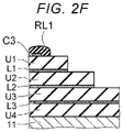
- a step structure that includes two steps can be formed, as shown in FIG. 2F .
- the height of the steps are determined by the thickness of the plurality of upper layers and the plurality of lower layers. Therefore, it is possible to obtain one or more steps respectively having a highly precise specified height.
- a precision of a width of the respective steps is determined by a precision of the plurality of cover layers (e.g. the first cover layer C 1 and the second cover layer C 2 ).
- the first energy ray ER 1 is radiated with high precision.
- an acceptable maximum error of the width of the steps corresponds to the width (the second length) of the second cover layer C 2 .
- the precision of the slimming may be low. Therefore, simple, inexpensive, and/or efficient manufacturing equipment can be implemented.
- the step structure can be formed with a high throughput.
- a template can be manufactured with high productivity.
- a step structure with three or more steps can be obtained by repeating at least some of the foregoing processes.
- the stacked body 12 further includes the third lower layer L 3 including the first material, the third upper layer U 3 including the second material, and the third cover layer C 3 including the third material.
- the third lower layer L 3 is provided between the second lower layer L 2 and the first substrate 11 .
- the third upper layer U 3 is provided between the third lower layer L 3 and the second lower layer L 2 .
- the third cover layer C 3 is provided on the third cover region R 3 of the first upper layer U 1 (see FIG. 1B ).
- portion of the first lower layer L 1 and portion of the second lower layer L 2 are exposed.
- the first resist layer RL 1 is processed to expose the second cover layer C 2 .
- the exposed second cover layer C 2 , the exposed portion of the first lower layer L 1 , and the exposed portion of the second lower layer L 2 are removed.
- the first material for example, chromium
- the first upper layer U 1 , a portion of the second upper layer U 2 , and a portion of the third upper layer U 3 are exposed.
- the surface of the layer including the second material for example, a silicon oxide
- the first resist layer RL 1 is processed to expose a portion of the third cover layer C 3 .
- the first resist layer RL 1 is subjected to slimming.
- an end portion of the third cover layer C 3 is exposed.
- the exposed portion of the first upper layer U 1 , the exposed portion of the second upper layer U 2 , and the exposed portion of the third upper layer U 3 are removed using the third cover layer C 3 and the first resist layer RL 1 as a mask.
- the second material for example, a silicon oxide
- the second material is etched.
- the first resist layer RL 1 is removed. Further, the exposed portions of the plurality of lower layers (the first lower layer L 1 , the second lower layer L 2 , and the third lower layer L 3 ) are removed.
- the first material for example, chromium
- a step structure with any number of steps can be obtained by repeating at least some of the processes described above.
- the radiations of the energy rays used for processing may be performed with different precisions.
- a template with high precision can be manufactured with high productivity.
- some embodiments of the template manufacturing method according to the first aspect includes forming the first cover layer C 1 .
- the forming of the first cover layer C 1 includes radiating the first energy ray ER 1 to the cover layer resist film Rcf provided on the cover film Cf to form the first cover layer C 1 .
- the forming of the first resist layer RL 1 includes radiating the second energy ray ER 2 to the first resist film Rf 1 to form the first resist layer RL 1 .
- the location precision in the radiation of the first energy ray ER 1 is higher than the location precision in the radiation of the second energy ray ER 2 .
- the location precision in the radiation of the second energy ray ER 2 may be relatively low.
- a template can be manufactured with high productivity.
- FIG. 4A through FIG. 4F are schematic sectional views showing embodiments of a pattern forming method using the template according to the first aspect.
- a first template 110 is prepared.
- the first template 110 includes the first substrate 11 and the stacked body 12 .
- a step structure 10 st of the first template 110 has a first surface 10 f that defines one or more steps.
- a resin liquid film 52 is provided on a processing substrate 51 .
- the resin liquid film 52 comes into contact with the step structure 10 st.
- the resin liquid film 52 is substantially solidified.
- the resin liquid film 52 has a photosetting property, and light (a third energy ray ER 3 ) is radiated.
- the layers provided in the first template 110 have transparency to the light.
- the resin liquid film 52 has a thermosetting property, and a heating treatment is performed.
- a solidified resin layer 52 L can be obtained from the resin liquid film 52 .
- the first template 110 is detached from the resin layer 52 L.
- the resin layer 52 L has a stepped surface shape that complements the first template 110 .
- an etching process 53 is performed.
- RIE reactive ion etching
- the processing substrate 51 is thus shaped to correspond to the shape of the resin layer 52 L.
- the processing substrate 51 includes a plurality of first films and a plurality of second films that are alternately stacked.
- the first films contain, for example, a silicon nitride.
- the second films contain, for example, a silicon oxide.
- One or more steps are formed in the stacked first and second films by imprinting performed using the first template 110 .
- a memory unit (a 3-dimensional memory cell) is provided in the stacked films.
- one of the first and second films is removed.
- the other of the first and second films remains.
- a conductive material for example, tungsten is introduced in a space created by the removal of the one of the first and second films.
- the plurality of conductive layers serve as, for example, wirings (for example, word lines) for a plurality of memory cells.
- the step portions serve as connection portions of the plurality of wirings.
- the template 110 according to the embodiment can be used to form the connection portions of the wirings of a 3-dimensional memory.
- FIG. 5A and FIG. 5B are schematic sectional views showing embodiments of the template according to the first aspect.
- FIG. 5B shows stepped portions of the first template 110 .
- FIG. 5A shows a state before the stepped portions are formed.
- FIG. 5A illustrates a template base member 210 used to form the first template 110 .
- the template base member 210 includes a plurality of first layers 61 and a plurality of second layers 62 that are alternately stacked.
- the first layer 61 is a layer including the first material, described above.
- the second layer 62 is a layer including the second material, described above.
- the second material is different from the first material.
- the thickness of the first layer 61 is less than the thickness of the second layer 62 .
- the first material includes, for example, chromium.
- the second material includes, for example, a silicon oxide (for example, quartz).
- the plurality of first layers 61 correspond to, for example, the plurality of lower layers (such as the first to third lower layers L 1 to L 3 ) described above.
- the plurality of second layers 62 correspond to, for example, the plurality of upper layers (such as the first to fourth upper layers U 1 to U 4 ) described above.
- One of the plurality of first layers 61 may correspond to the cover film Cf described above.
- layers including the third material may be provided on the uppermost layer (the uppermost second layer 62 ) and these layers may serve as the plurality of cover layers (the cover film Cf).
- the template base member 210 By using the template base member 210 , it is possible to form a template in accordance with the above-described manufacturing method.
- the first template 110 includes the stacked body 12 .
- the stacked body 12 includes a plurality of stacked films SF.
- Each of the plurality of stacked films SF includes a lower layer LL including the first material and an upper layer UL including the second material different from the first material.
- One of the lower layers LL is, for example, the first lower layer L 1 .
- One of the upper layers UL is, for example, the first upper layer U 1 .
- the upper layer UL is provided on the lower layer LL.
- the plurality of stacked films SF can define one or more steps of the first template 110 .
- the respective thicknesses of the lower layers LL are substantially the same as each other.
- the respective thicknesses of the upper layers UL are substantially the same as each other.
- the first template 110 includes the step structure 10 st that has a first surface 10 f .
- the respective heights of the steps of the step structure 10 st defined by the plurality of stacked films SF are substantially the same as each other.
- the widths of exposed top surfaces (“terrace” surfaces) of the steps defined by the plurality of stacked films SF are substantially the same as each other.
- the width of each terrace surface corresponds to, for example, a pitch of a plurality of cover layers used in manufacture of the first template 110 .
- Embodiments according to the second aspect relate to a template manufacturing method that uses a template according to the first aspect.
- the first template 110 serving as a reference is formed according to the first embodiment.
- the first template 110 is, for example, a master template.
- a second template is manufactured using the first template 110 .
- a pattern for a semiconductor device or the like may be formed using the second template.
- FIG. 6A through 6F are schematic sectional views showing embodiments of a method of manufacturing a template according to the second aspect.
- the first template 110 is prepared or provided.
- the first template 110 includes a plurality of stacked films SF (see FIG. 5B ).
- Each of the plurality of stacked films SF includes a lower layer LL including a first material and an upper layer UL including a second material different from the first material.
- the first template 110 includes a first surface 10 f .
- a step structure 10 st of the first template 110 has a first surface 10 f that defines one or more steps defined by the plurality of stacked films SF.
- a resin liquid serving as a resin liquid film 52 is applied onto the first surface 10 f of the step structure 10 st .
- the resin liquid can serve as, for example, a resist.
- a second substrate 21 is placed on the resin liquid film 52 .
- the second substrate 21 is, for example, a silicon oxide substrate (for example, a quartz substrate).
- the resin liquid film 52 is provided between the first surface 10 f and the second substrate 21 .
- the resin liquid film 52 is substantially solidified to form a resin layer 52 L in a state in which the resin liquid film 52 provided between the first surface 10 f and the second substrate 21 comes into contact with the first surface 10 f .
- an ultraviolet ray is radiated to the resin liquid film 52 .
- the ultraviolet ray may be transmitted through the second substrate 21 (quartz substrate).
- the resin liquid film 52 is solidified to obtain the resin layer 52 L.
- the surface of the resin layer 52 L has a shape corresponding to a shape of the first surface 10 f of the step structure 10 st.
- the second substrate 21 is processed using the resin layer 52 L as a mask.
- the silicon oxide material for example, quartz
- the silicon oxide material is etched.
- a shape corresponding to the first surface 10 f of the step structure 10 st is defined by the second substrate 21 .
- a second template 120 can be obtained.
- the second substrate 21 has a second surface shape 20 C to which a shape of the step structure 10 st corresponds.
- a shape of the second surface shape 20 C may be a reverse of the shape of the step structure 10 st of the first template 110 (e.g. depressions of the step structure 10 st may correspond to protrusions of the second surface shape 20 C, and protrusions of the step structure 10 st may correspond to depressions of the second surface shape 20 C).
- a third template may be manufactured from the second template 120 in accordance with the same method.
- the third template may have a similar or same shape as the step structure 10 st of the first template 110 .
- steps may thus be provided in writing connection portions.
- the steps may be formed by, for example, nano-imprinting.
- a plurality of pairs of stacked structures are provided on the substrate.
- the stacked structures contain a plurality of layers including different materials.
- a first material includes, for example, a metal or carbon.
- a second material is different from the first material.
- the second material is, for example, silicon oxide (for example, quartz).
- a plurality of layers (cover layers) including a material different from the second material are formed on the surface of the substrate.
- the plurality of layers have a predetermined width, and may be spaced from each other at a predetermined interval.
- a first process and a second process may be performed.
- a portion of a surface of the substrate is covered with a resist (a first resist layer RL 1 ) that exposes a portion of the layer including the second material.
- the layer of the second material is etched using the resist and the layer on the surface as a mask.
- the layer including the first material is etched altering a region covered with the resist.
- the second step is repeated a plurality of times.
- the second process includes performing an etching process on the layer including the first material after performing an ashing process on the resist to contract the resist and changing a position of an end portion of the resist.
- the second process includes performing the ashing process on the resist to contract the resist.
- the second process may include forming an additional resist after removing the resist.
- the forming of the additional resist includes performing an exposure process and a development process on a material of which the additional resist is made.
- the exposure process includes, for example, at least one of laser radiation and electron ray radiation.
- the second process includes performing the asking process on the resist to contract the resist.
- the second process may include forming the additional resist after removing the resist.
- the forming of the additional resist may include, for example, performing ink jet application of a resist liquid and solidifying the resist liquid by radiation of light (for example, ultraviolet ray).
- a step is formed by performing a cycle of slimming ⁇ chromium etching ⁇ slimming ⁇ silicon oxide etching once. Thereafter, this process is repeated. Finally, the chromium film is peeled off. Thus, it is possible to obtain the template with the step shape.
- the number of repetitions can be repeated with a same resist.
- the resist When the resist is thinned so that the resist is resistant to the chromium etching or the silicon oxide etching, the resist may be peeled off. Then, another resist may be formed and the process can resume from an alignment drawing stage. In a process of fabricating multiple steps, the process can be performed with pattern precision corresponding to that of a first drawing.
- a template defining a step shape can be prepared at lower cost and with a higher throughput than in some comparative alignment drawing methods.
- drawing is performed with high precision.
- a precision of a width of a step to be formed corresponds to the first pattern forming precision.
- a precision of a height of the step corresponds to the precision of the thickness of the layer.
- strict etching precision is unnecessary.
- a step template can be readily formed with high quality.
- a stage of manufacture including changing a coverage of the resist can be readily performed.
- oxygen asking can be performed under time control.
- an end portion of the resist can readily be moved (e.g. contracted) to an intended position.
- a dry etching process can be performed as in some chromium etching or silicon oxide etching processes.
- the step can be formed by repeating an etching process using oxygen, chlorine, or fluorine.
- recovery to a start of a series of sequences can be performed after the resist is consumed and is resistant to etching.
- vertical and parallel are not strictly vertical and strictly parallel, but also include, for example, variations or the like in the manufacturing steps, and may be substantially vertical and substantially parallel.
- the terms “about” and “substantially” are used to describe and account for small variations. When used in conjunction with an event or circumstance, the terms “about” and “substantially” can refer to instances in which the event or circumstance occurs precisely as well as instances in which the event or circumstance occurs to a close approximation.
- the terms “about” and “substantially” can refer to a range of variation less than or equal to ⁇ 10% of that numerical value, such as less than or equal to ⁇ 5%, less than or equal to ⁇ 4%, less than or equal to ⁇ 3%, less than or equal to ⁇ 2%, less than or equal to ⁇ 1%, less than or equal to ⁇ 0.5%, less than or equal to ⁇ 0.1%, or less than or equal to ⁇ 0.05%.
- a component provided “on,” “above,” or “over” another component can encompass cases where the former component is directly on (e.g., in physical contact with) the latter component, as well as cases where one or more intervening components are located between the former component and the latter component.
Landscapes
- Engineering & Computer Science (AREA)
- Physics & Mathematics (AREA)
- General Physics & Mathematics (AREA)
- Mechanical Engineering (AREA)
- Health & Medical Sciences (AREA)
- Toxicology (AREA)
- Metallurgy (AREA)
- Chemical & Material Sciences (AREA)
- Organic Chemistry (AREA)
- Exposure Of Semiconductors, Excluding Electron Or Ion Beam Exposure (AREA)
- Moulds For Moulding Plastics Or The Like (AREA)
- Drying Of Semiconductors (AREA)
Abstract
Description
Claims (5)
Priority Applications (1)
| Application Number | Priority Date | Filing Date | Title |
|---|---|---|---|
| US17/688,275 US11762286B2 (en) | 2017-03-17 | 2022-03-07 | Template manufacturing method and template base member |
Applications Claiming Priority (3)
| Application Number | Priority Date | Filing Date | Title |
|---|---|---|---|
| JP2017053318A JP7023050B2 (en) | 2017-03-17 | 2017-03-17 | Template manufacturing method and template base material |
| JPJP2017-053318 | 2017-03-17 | ||
| JP2017-053318 | 2017-03-17 |
Related Child Applications (1)
| Application Number | Title | Priority Date | Filing Date |
|---|---|---|---|
| US17/688,275 Continuation US11762286B2 (en) | 2017-03-17 | 2022-03-07 | Template manufacturing method and template base member |
Publications (2)
| Publication Number | Publication Date |
|---|---|
| US20180267401A1 US20180267401A1 (en) | 2018-09-20 |
| US11294276B2 true US11294276B2 (en) | 2022-04-05 |
Family
ID=63521211
Family Applications (2)
| Application Number | Title | Priority Date | Filing Date |
|---|---|---|---|
| US15/695,847 Active 2039-10-16 US11294276B2 (en) | 2017-03-17 | 2017-09-05 | Template manufacturing method and template base member |
| US17/688,275 Active 2037-10-05 US11762286B2 (en) | 2017-03-17 | 2022-03-07 | Template manufacturing method and template base member |
Family Applications After (1)
| Application Number | Title | Priority Date | Filing Date |
|---|---|---|---|
| US17/688,275 Active 2037-10-05 US11762286B2 (en) | 2017-03-17 | 2022-03-07 | Template manufacturing method and template base member |
Country Status (2)
| Country | Link |
|---|---|
| US (2) | US11294276B2 (en) |
| JP (1) | JP7023050B2 (en) |
Families Citing this family (3)
| Publication number | Priority date | Publication date | Assignee | Title |
|---|---|---|---|---|
| JP7034696B2 (en) | 2017-12-14 | 2022-03-14 | キヤノン株式会社 | A method for manufacturing a cured product pattern, a method for manufacturing a processed circuit board, a method for manufacturing a circuit board, a method for manufacturing electronic components, and a method for manufacturing an imprint mold. |
| US12304114B2 (en) | 2019-09-27 | 2025-05-20 | Hoya Corporation | Method for manufacturing imprint mold, imprint mold, mold blank, and method for manufacturing optical element |
| EP3964356A1 (en) * | 2020-09-03 | 2022-03-09 | Boegli-Gravures SA | A method and system for manufacturing an embossing device by using an etch mask |
Citations (11)
| Publication number | Priority date | Publication date | Assignee | Title |
|---|---|---|---|---|
| US6475704B1 (en) * | 1997-09-12 | 2002-11-05 | Canon Kabushiki Kaisha | Method for forming fine structure |
| US20030215753A1 (en) * | 2002-05-17 | 2003-11-20 | Fan-Gang Tseng | Fabrication method of a three-dimensional microstructure |
| US20060279004A1 (en) | 2005-06-08 | 2006-12-14 | Canon Kabushiki Kaisha | Mold, pattern forming method, and pattern forming apparatus |
| JP2007042715A (en) | 2005-08-01 | 2007-02-15 | Toppan Printing Co Ltd | Imprint mold and manufacturing method thereof |
| US7396474B2 (en) | 2005-11-08 | 2008-07-08 | Arr-Maz Products, Lp | Dual injection of two polymeric filtration aids for gypsum removal from phosphoric acid/gypsum slurry |
| US7455789B2 (en) | 2002-08-01 | 2008-11-25 | Hitachi, Ltd. | Stamper, lithographic method of using the stamper and method of forming a structure by a lithographic pattern |
| JP2010171109A (en) | 2009-01-21 | 2010-08-05 | Toppan Printing Co Ltd | Imprinting mold precursor and method of manufacturing the imprinting mold precursor |
| US20110294072A1 (en) * | 2010-05-27 | 2011-12-01 | Samsung Electronics Co., Ltd. | Methods of manufacturing semiconductor devices using photolithography |
| US20110290759A1 (en) * | 2010-05-28 | 2011-12-01 | Furusho Kenji | Pattern formation method |
| JP2012023242A (en) | 2010-07-15 | 2012-02-02 | Toppan Printing Co Ltd | Pattern manufacturing method and pattern formed body formed thereby |
| JP2013077665A (en) | 2011-09-30 | 2013-04-25 | Toppan Printing Co Ltd | Pattern formation method and pattern formation body |
Family Cites Families (5)
| Publication number | Priority date | Publication date | Assignee | Title |
|---|---|---|---|---|
| US7422981B2 (en) | 2005-12-07 | 2008-09-09 | Canon Kabushiki Kaisha | Method for manufacturing semiconductor device by using dual damascene process and method for manufacturing article having communicating hole |
| US8318253B2 (en) | 2006-06-30 | 2012-11-27 | Asml Netherlands B.V. | Imprint lithography |
| US7914975B2 (en) | 2007-04-10 | 2011-03-29 | International Business Machines Corporation | Multiple exposure lithography method incorporating intermediate layer patterning |
| CN102478764B (en) | 2010-11-30 | 2013-08-07 | 中芯国际集成电路制造(北京)有限公司 | Dual graphing method |
| JP6266842B2 (en) | 2015-08-31 | 2018-01-24 | Hoya株式会社 | Mask blank, mask blank manufacturing method, phase shift mask, phase shift mask manufacturing method, and semiconductor device manufacturing method |
-
2017
- 2017-03-17 JP JP2017053318A patent/JP7023050B2/en active Active
- 2017-09-05 US US15/695,847 patent/US11294276B2/en active Active
-
2022
- 2022-03-07 US US17/688,275 patent/US11762286B2/en active Active
Patent Citations (13)
| Publication number | Priority date | Publication date | Assignee | Title |
|---|---|---|---|---|
| US6475704B1 (en) * | 1997-09-12 | 2002-11-05 | Canon Kabushiki Kaisha | Method for forming fine structure |
| US20030215753A1 (en) * | 2002-05-17 | 2003-11-20 | Fan-Gang Tseng | Fabrication method of a three-dimensional microstructure |
| US7455789B2 (en) | 2002-08-01 | 2008-11-25 | Hitachi, Ltd. | Stamper, lithographic method of using the stamper and method of forming a structure by a lithographic pattern |
| US20060279004A1 (en) | 2005-06-08 | 2006-12-14 | Canon Kabushiki Kaisha | Mold, pattern forming method, and pattern forming apparatus |
| JP2007140460A (en) | 2005-06-08 | 2007-06-07 | Canon Inc | Mold, pattern forming method, and pattern forming apparatus |
| JP2007042715A (en) | 2005-08-01 | 2007-02-15 | Toppan Printing Co Ltd | Imprint mold and manufacturing method thereof |
| JP5119579B2 (en) | 2005-08-01 | 2013-01-16 | 凸版印刷株式会社 | Imprint mold and manufacturing method thereof |
| US7396474B2 (en) | 2005-11-08 | 2008-07-08 | Arr-Maz Products, Lp | Dual injection of two polymeric filtration aids for gypsum removal from phosphoric acid/gypsum slurry |
| JP2010171109A (en) | 2009-01-21 | 2010-08-05 | Toppan Printing Co Ltd | Imprinting mold precursor and method of manufacturing the imprinting mold precursor |
| US20110294072A1 (en) * | 2010-05-27 | 2011-12-01 | Samsung Electronics Co., Ltd. | Methods of manufacturing semiconductor devices using photolithography |
| US20110290759A1 (en) * | 2010-05-28 | 2011-12-01 | Furusho Kenji | Pattern formation method |
| JP2012023242A (en) | 2010-07-15 | 2012-02-02 | Toppan Printing Co Ltd | Pattern manufacturing method and pattern formed body formed thereby |
| JP2013077665A (en) | 2011-09-30 | 2013-04-25 | Toppan Printing Co Ltd | Pattern formation method and pattern formation body |
Non-Patent Citations (1)
| Title |
|---|
| J. Micromech. Microeng. 20 (2010) 115012 (Year: 2010). * |
Also Published As
| Publication number | Publication date |
|---|---|
| US20220187704A1 (en) | 2022-06-16 |
| JP2018157093A (en) | 2018-10-04 |
| US11762286B2 (en) | 2023-09-19 |
| US20180267401A1 (en) | 2018-09-20 |
| JP7023050B2 (en) | 2022-02-21 |
Similar Documents
| Publication | Publication Date | Title |
|---|---|---|
| US20220187704A1 (en) | Template manufacturing method and template base member | |
| US9818611B2 (en) | Methods of forming etch masks for sub-resolution substrate patterning | |
| US8476170B2 (en) | Method of forming pattern, method of manufacturing semiconductor device, and method of manufacturing template | |
| EP1387216B1 (en) | method of forming a structure by a lithographic pattern | |
| US20100264113A1 (en) | Template, method of manufacturing the same, and method of forming pattern | |
| US10115726B2 (en) | Method and system for forming memory fin patterns | |
| US20090166317A1 (en) | Method of processing substrate by imprinting | |
| WO2017087066A1 (en) | Methods of forming etch masks for sub-resolution substrate patterning | |
| US20110189438A1 (en) | Template, method of manufacturing template, and pattern forming method | |
| US10274822B2 (en) | Template and method of manufacturing semiconductor device | |
| KR102328551B1 (en) | A method of patterning a substrate using a plurality of layers of material | |
| JP6167609B2 (en) | Nanoimprint template, pattern formation method using nanoimprint template, and method for producing nanoimprint template | |
| US10031414B2 (en) | Template, method of manufacturing the same, and imprint method | |
| US20160167256A1 (en) | Method for producing nanoimprint mold | |
| JP4939994B2 (en) | Pattern forming method and semiconductor device manufacturing method | |
| US20090170033A1 (en) | Method of forming pattern of semiconductor device | |
| US7939451B2 (en) | Method for fabricating a pattern | |
| JP6357753B2 (en) | Manufacturing method of nanoimprint mold | |
| US20210302830A1 (en) | Method of manufacturing template, template, and method of manufacturing semiconductor device | |
| JP5983322B2 (en) | Method for forming pattern structure | |
| JP6019967B2 (en) | Pattern formation method | |
| US9032340B2 (en) | Layout decomposition method and method for manufacturing semiconductor device applying the same | |
| JP2013251431A (en) | Nano-imprint mold and manufacturing method of the same | |
| JP2016092360A (en) | Defect correction method and method of manufacturing microstructure body | |
| JP6019966B2 (en) | Pattern formation method |
Legal Events
| Date | Code | Title | Description |
|---|---|---|---|
| FEPP | Fee payment procedure |
Free format text: ENTITY STATUS SET TO UNDISCOUNTED (ORIGINAL EVENT CODE: BIG.); ENTITY STATUS OF PATENT OWNER: LARGE ENTITY |
|
| AS | Assignment |
Owner name: TOSHIBA MEMORY CORPORATION, JAPAN Free format text: ASSIGNMENT OF ASSIGNORS INTEREST;ASSIGNOR:KANAMITSU, SHINGO;REEL/FRAME:043858/0978 Effective date: 20170926 |
|
| STPP | Information on status: patent application and granting procedure in general |
Free format text: DOCKETED NEW CASE - READY FOR EXAMINATION |
|
| STPP | Information on status: patent application and granting procedure in general |
Free format text: NON FINAL ACTION MAILED |
|
| STPP | Information on status: patent application and granting procedure in general |
Free format text: RESPONSE TO NON-FINAL OFFICE ACTION ENTERED AND FORWARDED TO EXAMINER |
|
| STPP | Information on status: patent application and granting procedure in general |
Free format text: FINAL REJECTION MAILED |
|
| STPP | Information on status: patent application and granting procedure in general |
Free format text: DOCKETED NEW CASE - READY FOR EXAMINATION |
|
| STPP | Information on status: patent application and granting procedure in general |
Free format text: NON FINAL ACTION MAILED |
|
| STPP | Information on status: patent application and granting procedure in general |
Free format text: FINAL REJECTION MAILED |
|
| STPP | Information on status: patent application and granting procedure in general |
Free format text: RESPONSE AFTER FINAL ACTION FORWARDED TO EXAMINER |
|
| STPP | Information on status: patent application and granting procedure in general |
Free format text: NOTICE OF ALLOWANCE MAILED -- APPLICATION RECEIVED IN OFFICE OF PUBLICATIONS |
|
| AS | Assignment |
Owner name: K.K. PANGEA, JAPAN Free format text: MERGER;ASSIGNOR:TOSHIBA MEMORY CORPORATION;REEL/FRAME:058751/0995 Effective date: 20180801 Owner name: KIOXIA CORPORATION, JAPAN Free format text: CHANGE OF NAME;ASSIGNOR:TOSHIBA MEMORY CORPORATION;REEL/FRAME:058751/0266 Effective date: 20191001 Owner name: TOSHIBA MEMORY CORPORATION, JAPAN Free format text: CHANGE OF NAME;ASSIGNOR:K.K. PANGEA;REEL/FRAME:058670/0930 Effective date: 20180801 |
|
| STPP | Information on status: patent application and granting procedure in general |
Free format text: PUBLICATIONS -- ISSUE FEE PAYMENT VERIFIED |
|
| STCF | Information on status: patent grant |
Free format text: PATENTED CASE |
|
| MAFP | Maintenance fee payment |
Free format text: PAYMENT OF MAINTENANCE FEE, 4TH YEAR, LARGE ENTITY (ORIGINAL EVENT CODE: M1551); ENTITY STATUS OF PATENT OWNER: LARGE ENTITY Year of fee payment: 4 |