US11283356B2 - Method of assembling a DC-DC converter - Google Patents
Method of assembling a DC-DC converter Download PDFInfo
- Publication number
- US11283356B2 US11283356B2 US17/093,812 US202017093812A US11283356B2 US 11283356 B2 US11283356 B2 US 11283356B2 US 202017093812 A US202017093812 A US 202017093812A US 11283356 B2 US11283356 B2 US 11283356B2
- Authority
- US
- United States
- Prior art keywords
- inductor
- power stage
- stage transistor
- substrate
- discrete power
- Prior art date
- Legal status (The legal status is an assumption and is not a legal conclusion. Google has not performed a legal analysis and makes no representation as to the accuracy of the status listed.)
- Active
Links
Images


Classifications
-
- H—ELECTRICITY
- H02—GENERATION; CONVERSION OR DISTRIBUTION OF ELECTRIC POWER
- H02M—APPARATUS FOR CONVERSION BETWEEN AC AND AC, BETWEEN AC AND DC, OR BETWEEN DC AND DC, AND FOR USE WITH MAINS OR SIMILAR POWER SUPPLY SYSTEMS; CONVERSION OF DC OR AC INPUT POWER INTO SURGE OUTPUT POWER; CONTROL OR REGULATION THEREOF
- H02M3/00—Conversion of dc power input into dc power output
- H02M3/02—Conversion of dc power input into dc power output without intermediate conversion into ac
- H02M3/04—Conversion of dc power input into dc power output without intermediate conversion into ac by static converters
- H02M3/10—Conversion of dc power input into dc power output without intermediate conversion into ac by static converters using discharge tubes with control electrode or semiconductor devices with control electrode
- H02M3/145—Conversion of dc power input into dc power output without intermediate conversion into ac by static converters using discharge tubes with control electrode or semiconductor devices with control electrode using devices of a triode or transistor type requiring continuous application of a control signal
- H02M3/155—Conversion of dc power input into dc power output without intermediate conversion into ac by static converters using discharge tubes with control electrode or semiconductor devices with control electrode using devices of a triode or transistor type requiring continuous application of a control signal using semiconductor devices only
- H02M3/156—Conversion of dc power input into dc power output without intermediate conversion into ac by static converters using discharge tubes with control electrode or semiconductor devices with control electrode using devices of a triode or transistor type requiring continuous application of a control signal using semiconductor devices only with automatic control of output voltage or current, e.g. switching regulators
- H02M3/158—Conversion of dc power input into dc power output without intermediate conversion into ac by static converters using discharge tubes with control electrode or semiconductor devices with control electrode using devices of a triode or transistor type requiring continuous application of a control signal using semiconductor devices only with automatic control of output voltage or current, e.g. switching regulators including plural semiconductor devices as final control devices for a single load
- H02M3/1588—Conversion of dc power input into dc power output without intermediate conversion into ac by static converters using discharge tubes with control electrode or semiconductor devices with control electrode using devices of a triode or transistor type requiring continuous application of a control signal using semiconductor devices only with automatic control of output voltage or current, e.g. switching regulators including plural semiconductor devices as final control devices for a single load comprising at least one synchronous rectifier element
-
- H—ELECTRICITY
- H01—ELECTRIC ELEMENTS
- H01L—SEMICONDUCTOR DEVICES NOT COVERED BY CLASS H10
- H01L27/00—Devices consisting of a plurality of semiconductor or other solid-state components formed in or on a common substrate
- H01L27/02—Devices consisting of a plurality of semiconductor or other solid-state components formed in or on a common substrate including semiconductor components specially adapted for rectifying, oscillating, amplifying or switching and having at least one potential-jump barrier or surface barrier; including integrated passive circuit elements with at least one potential-jump barrier or surface barrier
- H01L27/0203—Particular design considerations for integrated circuits
- H01L27/0207—Geometrical layout of the components, e.g. computer aided design; custom LSI, semi-custom LSI, standard cell technique
-
- H—ELECTRICITY
- H05—ELECTRIC TECHNIQUES NOT OTHERWISE PROVIDED FOR
- H05K—PRINTED CIRCUITS; CASINGS OR CONSTRUCTIONAL DETAILS OF ELECTRIC APPARATUS; MANUFACTURE OF ASSEMBLAGES OF ELECTRICAL COMPONENTS
- H05K1/00—Printed circuits
- H05K1/18—Printed circuits structurally associated with non-printed electric components
- H05K1/181—Printed circuits structurally associated with non-printed electric components associated with surface mounted components
-
- H—ELECTRICITY
- H05—ELECTRIC TECHNIQUES NOT OTHERWISE PROVIDED FOR
- H05K—PRINTED CIRCUITS; CASINGS OR CONSTRUCTIONAL DETAILS OF ELECTRIC APPARATUS; MANUFACTURE OF ASSEMBLAGES OF ELECTRICAL COMPONENTS
- H05K2201/00—Indexing scheme relating to printed circuits covered by H05K1/00
- H05K2201/10—Details of components or other objects attached to or integrated in a printed circuit board
- H05K2201/10007—Types of components
- H05K2201/1003—Non-printed inductor
-
- Y—GENERAL TAGGING OF NEW TECHNOLOGICAL DEVELOPMENTS; GENERAL TAGGING OF CROSS-SECTIONAL TECHNOLOGIES SPANNING OVER SEVERAL SECTIONS OF THE IPC; TECHNICAL SUBJECTS COVERED BY FORMER USPC CROSS-REFERENCE ART COLLECTIONS [XRACs] AND DIGESTS
- Y02—TECHNOLOGIES OR APPLICATIONS FOR MITIGATION OR ADAPTATION AGAINST CLIMATE CHANGE
- Y02B—CLIMATE CHANGE MITIGATION TECHNOLOGIES RELATED TO BUILDINGS, e.g. HOUSING, HOUSE APPLIANCES OR RELATED END-USER APPLICATIONS
- Y02B70/00—Technologies for an efficient end-user side electric power management and consumption
- Y02B70/10—Technologies improving the efficiency by using switched-mode power supplies [SMPS], i.e. efficient power electronics conversion e.g. power factor correction or reduction of losses in power supplies or efficient standby modes
Definitions
- the instant application relates to DC-DC converters, and more particularly to optimal placement of discrete power stage components of a DC-DC converter on a circuit board.
- DC-DC converters include active and passive components, including discrete power stage components such as discrete high-side and low-side power transistor dies, for regulating the voltage of a load such as a processor. Each pair of discrete high-side and low-side power transistor dies forms an output phase of the DC-DC converter which is coupled to the load by a corresponding output inductor.
- the components of a DC-DC converter, including the output inductors, are attached to a printed circuit board (PCB) together with the load.
- the PCB has various electrical pathways for electrically interconnecting the DC-DC converter components, including electrically connecting the discrete power stage transistor dies of the converter to the load.
- DC-DC converter power stage dies are conventionally attached to a PCB in the same plane as the output inductors, increasing the size of the PCB. Also, conventional layout design practices for PCBs further complicate such an arrangement of the DC-DC converter components.
- the DC-DC converter comprises a substrate having opposing first and second sides, a first discrete power stage transistor die attached to the first side of the substrate and comprising a high-side power transistor, and a second discrete power stage transistor die attached to the first side of the substrate and comprising a low-side power transistor electrically connected to the high-side power transistor to form an output phase of the DC-DC converter.
- the DC-DC converter further comprises an inductor attached to the first side of the substrate so as to electrically connect the output phase to a metal output trace on the substrate. The inductor at least partly covers at least one of the first and the second discrete power stage transistor dies.
- the method comprises: attaching a first discrete power stage transistor die to a first side of a substrate, the first discrete power stage transistor die comprising a high-side power transistor; attaching a second discrete power stage transistor die to the first side of the substrate, the second discrete power stage transistor die comprising a low-side power transistor electrically connected to the high-side power transistor to form an output phase of the DC-DC converter; attaching an inductor to the first side of the substrate so as to electrically connect the output phase to a metal output trace on the substrate, the inductor partly covering at least one of the first and the second discrete power stage transistor dies so that a plurality of pins of each discrete power stage transistor die partly covered by the inductor are uncovered by the inductor; and visually inspecting the plurality of pins uncovered by the inductor.
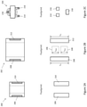
- FIG. 1A illustrates a top plan view of a section of a substrate such as a PCB to which power stage components of a DC-DC converter are attached, according to an embodiment.
- FIG. 1B shows the substrate of FIG. 1A after the power stage components of the DC-DC converter are attached to the substrate.
- FIG. 10 shows top, front and side views of the power stage inductor attached to the substrate shown in FIG. 1B .
- FIGS. 2A through 2C illustrate bottom plan views of different embodiments of output (phase) inductors designed to at least partly cover one or more discrete power stage transistor dies of a DC-DC converter.
- FIGS. 3A through 5A and 3B through 5B illustrate respective top-down plan views of different embodiments of a section of a substrate to which power stage components of a DC-DC converter are to be attached.
- FIGS. 6A through 8A and 6B through 8B illustrate respective top-down plan views of additional different embodiments of a section of a substrate to which power stage components of a DC-DC converter are to be attached.
- FIGS. 9A through 11A and 9B through 11B illustrate respective top-down plan views of yet additional different embodiments of a section of a substrate to which power stage components of a DC-DC converter are to be attached.
- FIG. 12 illustrates a side perspective view of a coupled inductor designed to at least partly cover one or more discrete power stage transistor dies of a DC-DC converter.
- a DC-DC converter includes at least one pair of discrete power stage transistor dies.
- Each discrete power stage transistor die includes a high-side power transistor or a low-side power transistor, but not both transistors.
- the power transistors which form the power (output) stage of the DC-DC converter are disposed in separate dies.
- Each discrete high-side transistor die switchably connects the load to an input voltage of the DC-DC converter, and the corresponding discrete low-side transistor die switchably connects the load to ground at different periods.
- the discrete dies can be bare dies i.e. unpackaged dies and have a thickness of 0.6 mm or less.
- the discrete dies are packaged dies such as a molded die package or an open cavity die package each having a thickness of 1.1 mm or less.
- each pair of discrete high-side and low-side power stage transistor dies forms an output phase of the DC-DC converter.
- Each output phase is coupled to the load by a respective inductor.
- the DC-DC converter is a single-phase converter.
- the DC-DC converter is a multi-phase converter.
- One or more of the discrete power stage transistor dies is at least partly covered by the inductor electrically coupled to that phase.
- a plurality of pins of that discrete die can remain uncovered by the inductor, which allows for easy visual inspection of those pins after the components of the DC-DC converter are attached to a substrate such as a circuit board.
- FIG. 1A illustrates a top-down plan view of a section of a substrate 100 such as a PCB (printed circuit board) to which power stage components of a DC-DC converter are to be attached.
- FIG. 1A illustrates the substrate 100 prior to attachment of the power stage components. As such, only the footprints of the power stage components are shown in FIG. 1A .
- the DC-DC converter can be a single-phase or a multi-phase converter as explained above.
- the section of the substrate 100 shown in FIG. 1A can correspond to one phase of a single-phase or one phase of a multi-phase converter where the physical layout of each phase can be identical or different to what is shown in FIG. 1A for the one phase. That is, the output phase layout shown in FIG. 1A can be replicated for each phase of a multi-phase converter or the output phases can have different layouts.
- the power stage components of the single-phase or multi-phase DC-DC converter include input capacitors 102 , output capacitors 104 , discrete high-side and low-side power transistor dies 106 , 108 for each phase of the DC-DC converter, and an inductor 110 for coupling each phase to a load regulated by the DC-DC converter.
- the pair of discrete high-side and low-side transistor dies 106 , 108 shown in FIG. 1A forms one output phase of the DC-DC converter, which is coupled to the load by the inductor 110 .
- FIG. 1A A circuit schematic of the phase formed by the high-side transistor Q 1 included in the discrete high-side transistor die 106 , the low-side transistor Q 2 included in the discrete low-side transistor die 108 , and the inductor 110 is shown in FIG. 1A .
- the load can be a high-performance integrated circuit such as a microprocessor, graphics processor, network processor, etc. or other type of integrated circuit requiring voltage regulation such as a POL (point-of-load). The load is not shown in FIG. 1A for ease of illustration.
- the substrate 100 includes various metal traces such as copper traces for electrically connecting the power stage components.
- the metal traces are separated from one another to prevent shorting.
- the metal traces include an input trace 112 which is at the input voltage potential (Vin) of the DC-DC converter, an output trace 114 which is at the regulated output voltage potential (Vout) of the DC-DC converter, one or more ground traces 116 , 118 connected to ground, and a phase trace 120 .
- the input capacitors 102 of the power stage are connected between the input trace 112 and one of the ground traces 116 .
- the output capacitors 104 of the power stage are connected between the output trace 114 and one of the ground traces 118 .
- the input side of the discrete high-side transistor die 106 is connected to the input trace 112 , so that the high-side transistor Q 1 included in the discrete high-side transistor die 106 can switchably connect the load to the input voltage Vin of the DC-DC converter.
- the input side of the discrete low-side transistor die 108 is connected to one of the ground traces 116 , so that the low-side transistor Q 2 included in the discrete low-side transistor die 108 can switchably connect the load to ground at different periods than the high-side transistor Q 1 is active.
- the output side of both discrete transistor dies 106 , 108 are connected to the phase trace 120 .
- One terminal of the inductor 110 is attached to the phase trace 120 and the other terminal of the inductor 110 is attached to the output trace 114 , so that the output sides of the discrete transistor dies 106 , 108 are electrically connected to the output trace 114 on the substrate 100 through the inductor 110 .
- FIG. 1B shows the substrate 100 after the power stage components of the DC-DC converter are attached to the substrate 100 .
- the inductor 110 completely covers both discrete power stage transistor dies 106 , 108 .
- the inductor 110 and the discrete power stage transistor dies 106 , 108 have overlapping footprints so that when the inductor 110 is attached to the substrate 100 , the inductor 110 provides sufficient clearance such that both discrete power stage transistor dies 106 , 108 are underneath and fully or partly covered by the inductor 110 .
- the metal ground trace 116 to which the discrete low-side transistor die 108 is connected, the input trace 112 and the phase trace 120 are each completely covered by the inductor 110 as shown in FIG. 1B .
- FIG. 1C shows a top view, side view and front view of the inductor 110 .
- the inductor 110 is a single inductor according to this embodiment which comprises a single winding 122 wound on a core 124 .
- the single winding 122 electrically connects the phase trace 120 to the output trace 114 of the substrate 100 . More particularly, the inductor 110 comprises a first terminal 126 electrically connected to the phase trace 120 and therefore to the output phase formed by the discrete high-side and low-side transistor dies 106 , 108 .
- a second terminal (out of view) of the inductor 110 is attached to the output trace 114 .
- the single winding 122 of the inductor 110 e.g.
- a copper foil winding is connected between the first and second terminals and forms part of the main body of the inductor 110 .
- the main body of the inductor 110 is spaced apart from the substrate 100 by a gap 128 .
- the main body of the inductor 110 also comprises a plastic riser 130 for providing clearance 128 under inductor 110 .
- This clearance 128 provides the gap between the inductor 110 and the substrate 100 for accommodating at least one of the discrete power stage transistor dies 106 , 108 under the inductor 110 .
- both discrete power stage transistor dies 106 , 108 are disposed in the gap 128 and completely covered by the inductor 110 .
- the bottom surface of the inductor 110 facing the substrate 100 is spaced apart from the top surface of each discrete power stage transistor die 106 , 108 at least partly covered by the inductor 110 by at least 0.1 mm.
- FIGS. 2A through 2C illustrate bottom plan view of different embodiments of output (phase) inductors 200 , 202 , 204 designed to at least partly cover one or more discrete power stage transistor dies of a DC-DC converter.
- the footprint of the respective inductors 200 , 202 , 204 also is shown in FIGS. 2A through 2C , the footprint corresponding to the amount of space on the substrate needed for attaching the respective inductors 200 , 202 , 204 to the substrate.
- FIGS. 2A and 2B just the two terminals 206 / 208 , 210 / 212 of the corresponding inductor 200 / 202 are attached to the substrate.
- the lengths L T1 , L T2 of the first and second terminals 208 , 212 of the inductor 202 in FIG. 2B are individually longer than the combined length (L DHS +L DLS ) of the discrete high-side and low-side power stage transistor dies 106 , 108 .
- the discrete high-side and low-side transistor dies 106 , 108 are illustrated with respective dashed boxes in FIG. 2B to show the corresponding die footprint in relation to the length of the inductor terminals 208 , 212 .
- the inductor 204 shown in FIG. 2C has an additional post 218 for stabilizing the inductor 204 after attachment to a substrate.
- FIGS. 3A through 5A and 3B through 5B illustrate respective top-down plan views of different embodiments of a section of a substrate 300 such as a PCB (printed circuit board) to which power stage components of a DC-DC converter are to be attached.
- FIGS. 3A through 5A illustrate the respective substrate sections prior to assembly of the power stage components
- FIGS. 3B through 5B illustrate the same substrate sections after power stage component attachment. As such, FIGS. 3A through 5A show only the footprints of the power stage components.
- the DC-DC converter can be a single-phase or a multi-phase converter and the power stage components of the DC-DC converter include input capacitors 302 , output capacitors 304 , discrete high-side and low-side power transistor dies 306 , 308 for each phase of the DC-DC converter, and an inductor 310 for coupling each phase to a load regulated by the DC-DC converter as previously explained herein.
- the substrate 300 includes various metal traces such as copper traces for electrically connecting the power stage components.
- the metal traces are separated from one another to prevent shorting.
- the metal traces include an input trace 312 which is at the input voltage potential (Vin) of the DC-DC converter, an output trace 314 which is at the regulated output voltage potential (Vout) of the DC-DC converter, one or more ground traces 316 , 318 connected to ground, and a phase trace 320 also as previously described herein.
- the input capacitors 302 of the power stage are connected between the input trace 312 and one of the ground traces 316 .
- the output capacitors 304 of the power stage are connected between the output trace 314 and one of the ground traces 318 .
- the discrete high-side transistor die 306 is electrically connected between the input trace 312 and the phase trace 320 .
- the discrete low-side transistor die 308 is electrically connected between one of the ground traces 316 and the phase trace 320 .
- One terminal 322 of the inductor 310 is attached to the phase trace 320 and the other terminal 324 is attached to the output trace 314 , so that the outputs of the discrete transistor dies 306 , 308 are electrically connected to the output trace 314 on the substrate 300 through the inductor 310 .
- the inductor 310 completely covers the discrete low-side transistor die 308 and does not cover any part of the discrete high-side transistor die 306 .
- the discrete low-side transistor die 308 is disposed in the gap between the main body of the inductor 310 and the substrate 300 as previously described herein.
- the inductor 310 at least partly covers both discrete transistor dies 306 , 308 .
- the discrete high-side transistor die 306 is partly covered by the inductor 310 and the discrete low-side transistor die 308 is completely covered by the inductor 310 . This way, the pins 326 of each discrete high-side transistor die 306 , 308 which remain uncovered by the inductor 310 can be visually inspected without interference from the inductor 310 .
- the inductor 310 partly covers the discrete low-side transistor die 308 and does not cover any part of the discrete high-side transistor die 306 .
- the discrete low-side transistor die 308 is disposed between the terminals 322 , 324 of the inductor 310 .
- the discrete low-side transistor die 308 is disposed adjacent to one of the inductor terminals 322 , but not between the inductor terminals 322 , 324 .
- the phase trace 320 extends under the inductor 310 .
- FIGS. 3B and 5B the phase trace 320 extends under the inductor 310 .
- one of the ground traces 316 extends under the inductor 310 .
- the discrete low-side transistor die 308 is attached to both this ground trace 316 and the phase trace 320 in a first region of the substrate 300 disposed under the inductor 310 .
- FIGS. 6A through 8A and 6B through 8B illustrate respective top-down plan views of additional different embodiments of a section of a substrate 400 such as a PCB (printed circuit board) to which power stage components of a DC-DC converter are to be attached.
- FIGS. 6A through 8A illustrate the respective substrate sections prior to assembly of the power stage components
- FIGS. 6B through 8B illustrate the same substrate sections after power stage component attachment. As such, FIGS. 6A through 8A show only the footprints of the power stage components.
- the DC-DC converter can be a single-phase or a multi-phase converter and the power stage components of the DC-DC converter include input capacitors 302 , output capacitors 304 , discrete high-side and low-side power transistor dies 306 , 308 for each phase of the DC-DC converter, and an inductor 310 for coupling each phase to a load regulated by the DC-DC converter as previously explained herein.
- FIGS. 6A through 8A and 6B through 8B are similar to those shown in FIGS. 3A through 5A and 3B through 5B , respectively.
- one or more of the substrate metal traces shown in FIGS. 6A through 8A and 6B through 8B have different layout configurations as compared to the respective layouts shown in FIGS. 3A through 5A and 3B through 5B .
- the input trace 312 extends under the inductor 310 and the discrete high-side transistor die 306 is attached to both the input trace 312 and the phase trace 120 in a second region of the substrate 400 disposed under the inductor 310 , the second region being different than the first region shown in FIGS.
- both discrete transistor dies 306 , 308 are disposed in the gap and adjacent to the first terminal 322 of the inductor 310 .
- FIGS. 5A and 5B only the discrete low-side transistor die 308 is disposed in the gap and adjacent to the first terminal 322 of the inductor 310 .
- the discrete high-side transistor die 308 remains completely uncovered by the inductor 310 in FIG. 5B .
- FIGS. 9A through 11A and 9B through 11B illustrate respective top-down plan views of yet additional different embodiments of a section of a substrate 500 such as a PCB (printed circuit board) to which power stage components of a DC-DC converter are to be attached.
- FIGS. 9A through 11A illustrate the respective substrate sections prior to assembly of the power stage components
- FIGS. 9B through 11B illustrate the same substrate sections after power stage component attachment. As such, FIGS. 9A through 11A show only the footprints of the power stage components.
- the DC-DC converter can be a single-phase or a multi-phase converter and the power stage components of the DC-DC converter include input capacitors 302 , output capacitors 304 , discrete high-side and low-side power transistor dies 306 , 308 for each phase of the DC-DC converter, and an inductor 310 for coupling each phase to a load regulated by the DC-DC converter as previously explained herein.
- FIGS. 9A through 11A and 9B through 11B are similar to those shown in FIGS. 6A through 8A and 6B through 8B , respectively.
- the discrete low-side transistor die 308 shown in FIGS. 9A through 11A and 9B through 11B have a physically larger size than the discrete high-side transistor die 306 .
- inductors can be used as the output phase inductor of a DC-DC converter and which partly covers at least one of the discrete transistor dies that form that phase.
- FIG. 3C a single winding inductor 110 is shown.
- FIG. 12 shows a perspective view of a coupled inductor 600 which can replace two or more single winding phase inductors of a DC-DC converter.
- the coupled inductor 600 comprises two or more separate windings (out of view) wound on the same core (also out of view).
- Each separate winding has a pair of terminals 602 , 604 for attachment to corresponding metal traces on a substrate, and is associated with one phase of a multi-phase DC-DC converter. That is, each separate winding electrically connects one output phase of a multi-phase DC-DC converter to the output trace of a substrate. This way, more than one phase can be realized using a single coupled inductor.
- one or more of the inductors can comprise separate uncoupled windings wound on the same core, and each of the separate uncoupled windings electrically connects one output phase to the output trace of the substrate.
- the inductor 600 at least partly covers at least one discrete power stage transistor die of a DC-DC converter. Based on the coupled inductor design shown in FIG. 12 , one or both discrete power stage transistor dies of at least two phases of a multi-phase DC-DC converter can be disposed between the terminals 602 , 604 of the coupled inductor and at least partly covered by the coupled inductor 600 .
Abstract
Description
Claims (22)
Priority Applications (1)
| Application Number | Priority Date | Filing Date | Title |
|---|---|---|---|
| US17/093,812 US11283356B2 (en) | 2015-05-29 | 2020-11-10 | Method of assembling a DC-DC converter |
Applications Claiming Priority (2)
| Application Number | Priority Date | Filing Date | Title |
|---|---|---|---|
| US14/726,009 US10855178B2 (en) | 2015-05-29 | 2015-05-29 | Discrete power stage transistor dies of a DC-DC converter under an inductor |
| US17/093,812 US11283356B2 (en) | 2015-05-29 | 2020-11-10 | Method of assembling a DC-DC converter |
Related Parent Applications (1)
| Application Number | Title | Priority Date | Filing Date |
|---|---|---|---|
| US14/726,009 Division US10855178B2 (en) | 2015-05-29 | 2015-05-29 | Discrete power stage transistor dies of a DC-DC converter under an inductor |
Publications (2)
| Publication Number | Publication Date |
|---|---|
| US20210057996A1 US20210057996A1 (en) | 2021-02-25 |
| US11283356B2 true US11283356B2 (en) | 2022-03-22 |
Family
ID=57399211
Family Applications (2)
| Application Number | Title | Priority Date | Filing Date |
|---|---|---|---|
| US14/726,009 Active 2038-03-04 US10855178B2 (en) | 2015-05-29 | 2015-05-29 | Discrete power stage transistor dies of a DC-DC converter under an inductor |
| US17/093,812 Active US11283356B2 (en) | 2015-05-29 | 2020-11-10 | Method of assembling a DC-DC converter |
Family Applications Before (1)
| Application Number | Title | Priority Date | Filing Date |
|---|---|---|---|
| US14/726,009 Active 2038-03-04 US10855178B2 (en) | 2015-05-29 | 2015-05-29 | Discrete power stage transistor dies of a DC-DC converter under an inductor |
Country Status (3)
| Country | Link |
|---|---|
| US (2) | US10855178B2 (en) |
| CN (1) | CN106208673B (en) |
| DE (1) | DE102016109781A1 (en) |
Families Citing this family (1)
| Publication number | Priority date | Publication date | Assignee | Title |
|---|---|---|---|---|
| CN109411454B (en) * | 2017-10-05 | 2021-05-18 | 成都芯源系统有限公司 | Circuit package for multiphase power converter |
Citations (53)
| Publication number | Priority date | Publication date | Assignee | Title |
|---|---|---|---|---|
| US5889387A (en) | 1996-12-13 | 1999-03-30 | Intel Corporation | Battery charging unit |
| US20030031339A1 (en) | 2000-01-13 | 2003-02-13 | Marshall Bowen F. | Packaging and rf shielding for telecoils |
| WO2003085476A1 (en) | 2002-04-03 | 2003-10-16 | International Rectifier Corporation | Synchronous buck converter improvements |
| JP2004063676A (en) | 2002-07-26 | 2004-02-26 | Fdk Corp | Micro-converter |
| US20050052888A1 (en) | 2003-08-20 | 2005-03-10 | Yoshihiro Takeshima | Switching power supply |
| JP2005102485A (en) | 2003-08-20 | 2005-04-14 | Matsushita Electric Ind Co Ltd | Switching power supply device |
| US20060279267A1 (en) | 2005-06-14 | 2006-12-14 | Intel Corporation | IC with fully integrated DC-to-DC power converter |
| JP2008092653A (en) | 2006-09-30 | 2008-04-17 | Nippon Chemicon Corp | Dc-dc converter |
| JP2008112941A (en) | 2006-10-31 | 2008-05-15 | Tdk Corp | Electronic component module |
| US20080284403A1 (en) | 2007-05-17 | 2008-11-20 | Analog Devices, Inc. | High-side current sense circuit with common-mode voltage reduction |
| JP3147172U (en) | 2008-10-06 | 2008-12-18 | トレックス・セミコンダクター株式会社 | Coil integrated DC / DC converter |
| US20090147541A1 (en) | 2007-12-11 | 2009-06-11 | Hitachi Computer Peripherals Co., Ltd. | Complex Inductor and Power Supply Unit |
| US20090207574A1 (en) | 2008-02-18 | 2009-08-20 | Cyntec Co., Ltd | Electronic package structure |
| US20090212391A1 (en) | 2008-02-25 | 2009-08-27 | Francesco Carobolante | Micromodules Including Integrated Thin Film Inductors and Methods of Making the Same |
| US20100085139A1 (en) | 2008-10-08 | 2010-04-08 | Cooper Technologies Company | High Current Amorphous Powder Core Inductor |
| US20100133670A1 (en) | 2008-12-01 | 2010-06-03 | Kai Liu | Top-side Cooled Semiconductor Package with Stacked Interconnection Plates and Method |
| JP2011019083A (en) | 2009-07-09 | 2011-01-27 | Nec Tokin Corp | Electronic composite component |
| US7880455B2 (en) | 2004-08-30 | 2011-02-01 | Monolithic Power Systems, Inc. | Short circuit current ratcheting in switch mode DC/DC voltage regulators |
| CN102088241A (en) | 2009-12-07 | 2011-06-08 | 英特赛尔美国股份有限公司 | Stacked inductor-electronic package assembly and technique for manufacturing the same |
| US8004070B1 (en) | 2008-04-29 | 2011-08-23 | Wei Chen | Wire-free chip module and method |
| US20110205008A1 (en) | 2010-02-19 | 2011-08-25 | Murata Power Solutions | High current inductor assembly |
| US20110228507A1 (en) | 2010-03-16 | 2011-09-22 | Intersil Americas Inc. | Molded power-supply module with bridge inductor over other components |
| US20110242775A1 (en) | 2010-04-02 | 2011-10-06 | Astec International Limited | Inductors Occupying Space Above Circuit Board Components |
| US20120069529A1 (en) | 2010-09-21 | 2012-03-22 | Cyntec Co., Ltd. | Power conversion module |
| JP2012109518A (en) | 2010-10-26 | 2012-06-07 | Kyocera Corp | Inductor component and electronic device |
| CN102763179A (en) | 2009-12-21 | 2012-10-31 | 沃特拉半导体公司 | Multi-Turn inductors |
| US20130099886A1 (en) | 2006-09-12 | 2013-04-25 | Cooper Technologies Company | High current magnetic component and methods of manufacture |
| CN103081325A (en) | 2010-05-24 | 2013-05-01 | 沃特拉半导体公司 | Two-phase coupled inductors which promote improved printed circuit board layout |
| US20130147559A1 (en) | 2011-12-09 | 2013-06-13 | Touchstone Semiconductor, Inc. | Fully differential autozeroing amplifier |
| US8471664B1 (en) | 2012-04-24 | 2013-06-25 | Zippy Technology Corp. | Transformer without coil racks |
| CN103227172A (en) | 2012-01-25 | 2013-07-31 | 英飞凌科技股份有限公司 | Integrated circuit including field effect transistor structures with gate and field electrodes and methods for manufacturing and operating an integrated circuit |
| CN103325783A (en) | 2012-03-22 | 2013-09-25 | 英飞凌科技股份有限公司 | Semiconductor chip and semiconductor arrangement |
| CN103367361A (en) | 2012-03-26 | 2013-10-23 | 英飞凌科技奥地利有限公司 | Semiconductor arrangement with a power transistor and a high voltage device |
| US20140062246A1 (en) | 2007-05-03 | 2014-03-06 | In Motion Technologies Pty., Ltd. | Rotor magnet positioning device |
| US20140062446A1 (en) | 2012-08-29 | 2014-03-06 | Alexandr Ikriannikov | Bridge Magnetic Devices And Associated Systems And Methods |
| CN103680861A (en) | 2013-11-27 | 2014-03-26 | 东莞普思电子有限公司 | Flat coil inductor, flat coil and manufacture method of flat coil |
| US20140159054A1 (en) | 2012-05-15 | 2014-06-12 | Rohm Co., Ltd. | Power module semiconductor device |
| US20140167900A1 (en) | 2012-12-14 | 2014-06-19 | Gregorio R. Murtagian | Surface-mount inductor structures for forming one or more inductors with substrate traces |
| US20140239472A1 (en) | 2013-02-28 | 2014-08-28 | Frank Tim Jones | Dual-flag stacked die package |
| CN104051128A (en) | 2013-03-15 | 2014-09-17 | 库柏技术公司 | High-performance heavy-current power inductor |
| US20140292459A1 (en) | 2013-03-27 | 2014-10-02 | General Electric Company | Magnetic device having integrated current sensing element and methods of assembling same |
| EP2866533A1 (en) | 2013-10-28 | 2015-04-29 | Infineon Technologies Austria AG | Dc-dc converter assembly with an output inductor accommodating a power stage attached to a circuit board |
| WO2015074247A1 (en) | 2013-11-22 | 2015-05-28 | Cooper Technologies Company | Surface mount power inductor component with stacked component accommodation |
| US20150162297A1 (en) | 2013-12-05 | 2015-06-11 | International Rectifier Corporation | Power Converter Package with an Integrated Output Inductor |
| US20150194374A1 (en) | 2014-01-07 | 2015-07-09 | Iinfineon Technologies Ag | Package with terminal pins with lateral reversal point and laterally exposed free end |
| US20150200156A1 (en) * | 2014-01-13 | 2015-07-16 | Altera Corporation | Module having mirror-symmetric terminals and methods of forming the same |
| US20150311655A1 (en) | 2012-11-08 | 2015-10-29 | Seok-Jae Han | Memory card adapter |
| US9190383B2 (en) | 2013-12-05 | 2015-11-17 | Infineon Technologies Americas Corp. | Semiconductor package including a power stage and integrated output inductor |
| US20160005528A1 (en) | 2013-03-15 | 2016-01-07 | Cooper Technologies Company | High performance high current power inductor |
| US20160163631A1 (en) * | 2014-12-03 | 2016-06-09 | International Business Machines Corporation | Chip carrier with dual-sided chip access and a method for testing a chip using the chip carrier |
| US20160164417A1 (en) | 2013-08-07 | 2016-06-09 | Panasonic Intellectual Property Management Co., Ltd. | Dc-dc converter module |
| US9729059B1 (en) | 2016-02-09 | 2017-08-08 | Faraday Semi, LLC | Chip embedded DC-DC converter |
| US9742304B2 (en) | 2013-10-09 | 2017-08-22 | Hitachi Automotive Systems, Ltd. | Driver board and power converter |
-
2015
- 2015-05-29 US US14/726,009 patent/US10855178B2/en active Active
-
2016
- 2016-05-25 CN CN201610355322.7A patent/CN106208673B/en active Active
- 2016-05-27 DE DE102016109781.0A patent/DE102016109781A1/en active Pending
-
2020
- 2020-11-10 US US17/093,812 patent/US11283356B2/en active Active
Patent Citations (63)
| Publication number | Priority date | Publication date | Assignee | Title |
|---|---|---|---|---|
| US5889387A (en) | 1996-12-13 | 1999-03-30 | Intel Corporation | Battery charging unit |
| US20030031339A1 (en) | 2000-01-13 | 2003-02-13 | Marshall Bowen F. | Packaging and rf shielding for telecoils |
| JP2005522173A (en) | 2002-04-03 | 2005-07-21 | インターナショナル・レクチファイヤー・コーポレーション | Synchronous buck converter |
| WO2003085476A1 (en) | 2002-04-03 | 2003-10-16 | International Rectifier Corporation | Synchronous buck converter improvements |
| US20040140877A1 (en) | 2002-07-26 | 2004-07-22 | Fumiaki Nakao | Microconverter and laminated magnetic-core inductor |
| US20050134420A1 (en) | 2002-07-26 | 2005-06-23 | Fdk Corporation | Microconverter and laminated magnetic-core inductor |
| JP2004063676A (en) | 2002-07-26 | 2004-02-26 | Fdk Corp | Micro-converter |
| JP2005102485A (en) | 2003-08-20 | 2005-04-14 | Matsushita Electric Ind Co Ltd | Switching power supply device |
| US20050052888A1 (en) | 2003-08-20 | 2005-03-10 | Yoshihiro Takeshima | Switching power supply |
| US7880455B2 (en) | 2004-08-30 | 2011-02-01 | Monolithic Power Systems, Inc. | Short circuit current ratcheting in switch mode DC/DC voltage regulators |
| US20060279267A1 (en) | 2005-06-14 | 2006-12-14 | Intel Corporation | IC with fully integrated DC-to-DC power converter |
| US20130099886A1 (en) | 2006-09-12 | 2013-04-25 | Cooper Technologies Company | High current magnetic component and methods of manufacture |
| JP2008092653A (en) | 2006-09-30 | 2008-04-17 | Nippon Chemicon Corp | Dc-dc converter |
| JP2008112941A (en) | 2006-10-31 | 2008-05-15 | Tdk Corp | Electronic component module |
| US20140062246A1 (en) | 2007-05-03 | 2014-03-06 | In Motion Technologies Pty., Ltd. | Rotor magnet positioning device |
| US20080284403A1 (en) | 2007-05-17 | 2008-11-20 | Analog Devices, Inc. | High-side current sense circuit with common-mode voltage reduction |
| US20090147541A1 (en) | 2007-12-11 | 2009-06-11 | Hitachi Computer Peripherals Co., Ltd. | Complex Inductor and Power Supply Unit |
| CN101552119A (en) | 2007-12-11 | 2009-10-07 | 日立计算机机器株式会社 | Complex inductor and power supply unit |
| US20090207574A1 (en) | 2008-02-18 | 2009-08-20 | Cyntec Co., Ltd | Electronic package structure |
| US20090212391A1 (en) | 2008-02-25 | 2009-08-27 | Francesco Carobolante | Micromodules Including Integrated Thin Film Inductors and Methods of Making the Same |
| US8004070B1 (en) | 2008-04-29 | 2011-08-23 | Wei Chen | Wire-free chip module and method |
| JP3147172U (en) | 2008-10-06 | 2008-12-18 | トレックス・セミコンダクター株式会社 | Coil integrated DC / DC converter |
| US20100085139A1 (en) | 2008-10-08 | 2010-04-08 | Cooper Technologies Company | High Current Amorphous Powder Core Inductor |
| US20100133670A1 (en) | 2008-12-01 | 2010-06-03 | Kai Liu | Top-side Cooled Semiconductor Package with Stacked Interconnection Plates and Method |
| JP2011019083A (en) | 2009-07-09 | 2011-01-27 | Nec Tokin Corp | Electronic composite component |
| CN102088241A (en) | 2009-12-07 | 2011-06-08 | 英特赛尔美国股份有限公司 | Stacked inductor-electronic package assembly and technique for manufacturing the same |
| US20110134613A1 (en) * | 2009-12-07 | 2011-06-09 | Intersil Americas Inc. | Stacked inductor-electronic package assembly and technique for manufacturing same |
| CN102763179A (en) | 2009-12-21 | 2012-10-31 | 沃特拉半导体公司 | Multi-Turn inductors |
| US20110205008A1 (en) | 2010-02-19 | 2011-08-25 | Murata Power Solutions | High current inductor assembly |
| US20110228507A1 (en) | 2010-03-16 | 2011-09-22 | Intersil Americas Inc. | Molded power-supply module with bridge inductor over other components |
| JP2011193000A (en) | 2010-03-16 | 2011-09-29 | Intersil Americas Inc | Molded power supply module with bridge inductor on other part and method of manufacturing the same |
| CN102254908A (en) | 2010-03-16 | 2011-11-23 | 英特赛尔美国股份有限公司 | Molded power-supply module with bridge inductor over other components |
| CN102256443A (en) | 2010-04-02 | 2011-11-23 | 雅达电子国际有限公司 | Inductors occupying space above circuit board components |
| US20110242775A1 (en) | 2010-04-02 | 2011-10-06 | Astec International Limited | Inductors Occupying Space Above Circuit Board Components |
| CN103081325A (en) | 2010-05-24 | 2013-05-01 | 沃特拉半导体公司 | Two-phase coupled inductors which promote improved printed circuit board layout |
| TW201215261A (en) | 2010-09-21 | 2012-04-01 | Cyntec Co Ltd | Power-converting module |
| US20120069529A1 (en) | 2010-09-21 | 2012-03-22 | Cyntec Co., Ltd. | Power conversion module |
| JP2012109518A (en) | 2010-10-26 | 2012-06-07 | Kyocera Corp | Inductor component and electronic device |
| US20130147559A1 (en) | 2011-12-09 | 2013-06-13 | Touchstone Semiconductor, Inc. | Fully differential autozeroing amplifier |
| CN103227172A (en) | 2012-01-25 | 2013-07-31 | 英飞凌科技股份有限公司 | Integrated circuit including field effect transistor structures with gate and field electrodes and methods for manufacturing and operating an integrated circuit |
| CN103325783A (en) | 2012-03-22 | 2013-09-25 | 英飞凌科技股份有限公司 | Semiconductor chip and semiconductor arrangement |
| CN103367361A (en) | 2012-03-26 | 2013-10-23 | 英飞凌科技奥地利有限公司 | Semiconductor arrangement with a power transistor and a high voltage device |
| US8471664B1 (en) | 2012-04-24 | 2013-06-25 | Zippy Technology Corp. | Transformer without coil racks |
| US20140159054A1 (en) | 2012-05-15 | 2014-06-12 | Rohm Co., Ltd. | Power module semiconductor device |
| US20140062446A1 (en) | 2012-08-29 | 2014-03-06 | Alexandr Ikriannikov | Bridge Magnetic Devices And Associated Systems And Methods |
| US9281739B2 (en) | 2012-08-29 | 2016-03-08 | Volterra Semiconductor LLC | Bridge magnetic devices and associated systems and methods |
| US20150311655A1 (en) | 2012-11-08 | 2015-10-29 | Seok-Jae Han | Memory card adapter |
| US20140167900A1 (en) | 2012-12-14 | 2014-06-19 | Gregorio R. Murtagian | Surface-mount inductor structures for forming one or more inductors with substrate traces |
| US20140239472A1 (en) | 2013-02-28 | 2014-08-28 | Frank Tim Jones | Dual-flag stacked die package |
| US20160005528A1 (en) | 2013-03-15 | 2016-01-07 | Cooper Technologies Company | High performance high current power inductor |
| CN104051128A (en) | 2013-03-15 | 2014-09-17 | 库柏技术公司 | High-performance heavy-current power inductor |
| US20140292459A1 (en) | 2013-03-27 | 2014-10-02 | General Electric Company | Magnetic device having integrated current sensing element and methods of assembling same |
| US20160164417A1 (en) | 2013-08-07 | 2016-06-09 | Panasonic Intellectual Property Management Co., Ltd. | Dc-dc converter module |
| US9742304B2 (en) | 2013-10-09 | 2017-08-22 | Hitachi Automotive Systems, Ltd. | Driver board and power converter |
| EP2866533A1 (en) | 2013-10-28 | 2015-04-29 | Infineon Technologies Austria AG | Dc-dc converter assembly with an output inductor accommodating a power stage attached to a circuit board |
| WO2015074247A1 (en) | 2013-11-22 | 2015-05-28 | Cooper Technologies Company | Surface mount power inductor component with stacked component accommodation |
| CN103680861A (en) | 2013-11-27 | 2014-03-26 | 东莞普思电子有限公司 | Flat coil inductor, flat coil and manufacture method of flat coil |
| US9190383B2 (en) | 2013-12-05 | 2015-11-17 | Infineon Technologies Americas Corp. | Semiconductor package including a power stage and integrated output inductor |
| US20150162297A1 (en) | 2013-12-05 | 2015-06-11 | International Rectifier Corporation | Power Converter Package with an Integrated Output Inductor |
| US20150194374A1 (en) | 2014-01-07 | 2015-07-09 | Iinfineon Technologies Ag | Package with terminal pins with lateral reversal point and laterally exposed free end |
| US20150200156A1 (en) * | 2014-01-13 | 2015-07-16 | Altera Corporation | Module having mirror-symmetric terminals and methods of forming the same |
| US20160163631A1 (en) * | 2014-12-03 | 2016-06-09 | International Business Machines Corporation | Chip carrier with dual-sided chip access and a method for testing a chip using the chip carrier |
| US9729059B1 (en) | 2016-02-09 | 2017-08-08 | Faraday Semi, LLC | Chip embedded DC-DC converter |
Non-Patent Citations (4)
| Title |
|---|
| "High Common-Mode Voltage, Single-Supply Difference Amplifier", Analog Devices; AD8202 Datasheet, Rev. H, 2004, pp. 1-20. |
| Unknown, Author, "60A Power Block Non-Isolated DC-DC Converter", Murata Power Solutions, Okami OKLP-X/60-W12A-C, Mansfield, MA, 2015, 1-12. |
| Unknown, Author, "Programmable Output 12-Amp iLGA SMT PoL DC-DC Converter Series", Murata Power Solutions, Okami OKL2-T/12-W12 Series, Mansfield, MA, 2014, 1-19. |
| Unknown, Author, "Programmable Output 3-Amp iLGA SMT PoLs", Murata Power Solutions, Okami OKL-T/3-W5 Series, Mansfield, MA, 2013, 1-17. |
Also Published As
| Publication number | Publication date |
|---|---|
| US10855178B2 (en) | 2020-12-01 |
| DE102016109781A1 (en) | 2017-03-16 |
| US20160352226A1 (en) | 2016-12-01 |
| US20210057996A1 (en) | 2021-02-25 |
| CN106208673B (en) | 2019-10-18 |
| CN106208673A (en) | 2016-12-07 |
Similar Documents
| Publication | Publication Date | Title |
|---|---|---|
| US9892851B2 (en) | DC-DC converter assembly, method of manufacturing a DC-DC converter assembly and method of manufacturing an output inductor for a DC-DC converter assembly | |
| US20170178797A1 (en) | Surface Mount Inductor for Placement Over a Power Stage of a Power Converter | |
| US8884719B2 (en) | Noise filter device | |
| US10367419B2 (en) | Power conversion device with integrated discrete inductor | |
| US10256719B2 (en) | Power supply device | |
| US20160261179A1 (en) | Methods and apparatus including integrated conducting and inductive element for providing current | |
| US11283356B2 (en) | Method of assembling a DC-DC converter | |
| US10050528B2 (en) | Current distribution in DC-DC converters | |
| US10714412B2 (en) | Semiconductor package with integrated passive electrical component | |
| US20170178795A1 (en) | Through-Hole Inductor for Placement Over a Power Stage of a Power Converter | |
| US20140159219A1 (en) | Multi-component chip packaging structure | |
| JP2001135770A (en) | Multifunctional lead frame and integrated circuit package incorporating the same | |
| US10333407B2 (en) | Power stage packages of a multi-phase DC-DC converter under a coupled inductor | |
| US11552049B2 (en) | Embedded power device module, processor substrate and electronic system | |
| JP2014236628A (en) | Dc high-voltage power supply device |
Legal Events
| Date | Code | Title | Description |
|---|---|---|---|
| AS | Assignment |
Owner name: INFINEON TECHNOLOGIES NORTH AMERICA CORP., CALIFORNIA Free format text: ASSIGNMENT OF ASSIGNORS INTEREST;ASSIGNORS:TANG, BENJAMIM;TSCHIRHART, DARRYL;TODOROV, EMIL;REEL/FRAME:054321/0487 Effective date: 20150527 |
|
| FEPP | Fee payment procedure |
Free format text: ENTITY STATUS SET TO UNDISCOUNTED (ORIGINAL EVENT CODE: BIG.); ENTITY STATUS OF PATENT OWNER: LARGE ENTITY |
|
| STPP | Information on status: patent application and granting procedure in general |
Free format text: APPLICATION DISPATCHED FROM PREEXAM, NOT YET DOCKETED |
|
| STPP | Information on status: patent application and granting procedure in general |
Free format text: DOCKETED NEW CASE - READY FOR EXAMINATION |
|
| STPP | Information on status: patent application and granting procedure in general |
Free format text: NOTICE OF ALLOWANCE MAILED -- APPLICATION RECEIVED IN OFFICE OF PUBLICATIONS |
|
| STCF | Information on status: patent grant |
Free format text: PATENTED CASE |
|
| AS | Assignment |
Owner name: INFINEON TECHNOLOGIES AMERICAS CORP., CALIFORNIA Free format text: MERGER AND CHANGE OF NAME;ASSIGNORS:INFINEON TECHNOLOGIES NORTH AMERICA CORP.;INTERNATIONAL RECTIFIER CORPORATION;REEL/FRAME:060617/0653 Effective date: 20150929 Owner name: INFINEON TECHNOLOGIES AUSTRIA AG, AUSTRIA Free format text: ASSIGNMENT OF ASSIGNORS INTEREST;ASSIGNOR:INFINEON TECHNOLOGIES AMERICAS CORP.;REEL/FRAME:060618/0220 Effective date: 20220715 |