US11282750B2 - Contact structure and method of fabricating the same - Google Patents
Contact structure and method of fabricating the same Download PDFInfo
- Publication number
- US11282750B2 US11282750B2 US17/010,995 US202017010995A US11282750B2 US 11282750 B2 US11282750 B2 US 11282750B2 US 202017010995 A US202017010995 A US 202017010995A US 11282750 B2 US11282750 B2 US 11282750B2
- Authority
- US
- United States
- Prior art keywords
- dielectric layer
- layer
- opening
- etch stop
- gate
- Prior art date
- Legal status (The legal status is an assumption and is not a legal conclusion. Google has not performed a legal analysis and makes no representation as to the accuracy of the status listed.)
- Active
Links
- 238000004519 manufacturing process Methods 0.000 title description 10
- 238000000034 method Methods 0.000 claims description 91
- 230000008569 process Effects 0.000 claims description 61
- 238000005530 etching Methods 0.000 claims description 37
- 239000000758 substrate Substances 0.000 claims description 34
- 229920002120 photoresistant polymer Polymers 0.000 claims description 32
- 239000004020 conductor Substances 0.000 claims description 18
- 238000000151 deposition Methods 0.000 claims description 11
- 229910052782 aluminium Inorganic materials 0.000 claims description 7
- XAGFODPZIPBFFR-UHFFFAOYSA-N aluminium Chemical compound [Al] XAGFODPZIPBFFR-UHFFFAOYSA-N 0.000 claims description 7
- 229910000449 hafnium oxide Inorganic materials 0.000 claims description 7
- TWNQGVIAIRXVLR-UHFFFAOYSA-N oxo(oxoalumanyloxy)alumane Chemical compound O=[Al]O[Al]=O TWNQGVIAIRXVLR-UHFFFAOYSA-N 0.000 claims description 7
- RVTZCBVAJQQJTK-UHFFFAOYSA-N oxygen(2-);zirconium(4+) Chemical compound [O-2].[O-2].[Zr+4] RVTZCBVAJQQJTK-UHFFFAOYSA-N 0.000 claims description 7
- 229910001928 zirconium oxide Inorganic materials 0.000 claims description 7
- WIHZLLGSGQNAGK-UHFFFAOYSA-N hafnium(4+);oxygen(2-) Chemical compound [O-2].[O-2].[Hf+4] WIHZLLGSGQNAGK-UHFFFAOYSA-N 0.000 claims description 5
- PMHQVHHXPFUNSP-UHFFFAOYSA-M copper(1+);methylsulfanylmethane;bromide Chemical compound Br[Cu].CSC PMHQVHHXPFUNSP-UHFFFAOYSA-M 0.000 claims 2
- 238000000059 patterning Methods 0.000 claims 1
- 125000006850 spacer group Chemical group 0.000 abstract description 51
- 239000010410 layer Substances 0.000 description 198
- 239000004065 semiconductor Substances 0.000 description 46
- 239000011229 interlayer Substances 0.000 description 25
- 239000000463 material Substances 0.000 description 12
- 239000003989 dielectric material Substances 0.000 description 11
- 238000000231 atomic layer deposition Methods 0.000 description 9
- XUIMIQQOPSSXEZ-UHFFFAOYSA-N Silicon Chemical compound [Si] XUIMIQQOPSSXEZ-UHFFFAOYSA-N 0.000 description 8
- 238000005229 chemical vapour deposition Methods 0.000 description 8
- 229910021332 silicide Inorganic materials 0.000 description 8
- FVBUAEGBCNSCDD-UHFFFAOYSA-N silicide(4-) Chemical group [Si-4] FVBUAEGBCNSCDD-UHFFFAOYSA-N 0.000 description 8
- 229910052710 silicon Inorganic materials 0.000 description 8
- 239000010703 silicon Substances 0.000 description 8
- 238000004140 cleaning Methods 0.000 description 7
- 229910052751 metal Inorganic materials 0.000 description 7
- 239000002184 metal Substances 0.000 description 7
- 238000002955 isolation Methods 0.000 description 6
- 229910052581 Si3N4 Inorganic materials 0.000 description 5
- 238000000623 plasma-assisted chemical vapour deposition Methods 0.000 description 5
- HQVNEWCFYHHQES-UHFFFAOYSA-N silicon nitride Chemical compound N12[Si]34N5[Si]62N3[Si]51N64 HQVNEWCFYHHQES-UHFFFAOYSA-N 0.000 description 5
- RTAQQCXQSZGOHL-UHFFFAOYSA-N Titanium Chemical compound [Ti] RTAQQCXQSZGOHL-UHFFFAOYSA-N 0.000 description 4
- 238000005137 deposition process Methods 0.000 description 4
- 238000010438 heat treatment Methods 0.000 description 4
- 230000004048 modification Effects 0.000 description 4
- 238000012986 modification Methods 0.000 description 4
- 229910021420 polycrystalline silicon Inorganic materials 0.000 description 4
- 229910052814 silicon oxide Inorganic materials 0.000 description 4
- 229910052719 titanium Inorganic materials 0.000 description 4
- 239000010936 titanium Substances 0.000 description 4
- RYGMFSIKBFXOCR-UHFFFAOYSA-N Copper Chemical compound [Cu] RYGMFSIKBFXOCR-UHFFFAOYSA-N 0.000 description 3
- KRHYYFGTRYWZRS-UHFFFAOYSA-N Fluorane Chemical compound F KRHYYFGTRYWZRS-UHFFFAOYSA-N 0.000 description 3
- VYPSYNLAJGMNEJ-UHFFFAOYSA-N Silicium dioxide Chemical compound O=[Si]=O VYPSYNLAJGMNEJ-UHFFFAOYSA-N 0.000 description 3
- 229910052802 copper Inorganic materials 0.000 description 3
- 239000010949 copper Substances 0.000 description 3
- 230000006870 function Effects 0.000 description 3
- 239000000126 substance Substances 0.000 description 3
- 229910052715 tantalum Inorganic materials 0.000 description 3
- GUVRBAGPIYLISA-UHFFFAOYSA-N tantalum atom Chemical compound [Ta] GUVRBAGPIYLISA-UHFFFAOYSA-N 0.000 description 3
- WFKWXMTUELFFGS-UHFFFAOYSA-N tungsten Chemical compound [W] WFKWXMTUELFFGS-UHFFFAOYSA-N 0.000 description 3
- 229910052721 tungsten Inorganic materials 0.000 description 3
- 239000010937 tungsten Substances 0.000 description 3
- 238000001039 wet etching Methods 0.000 description 3
- PIGFYZPCRLYGLF-UHFFFAOYSA-N Aluminum nitride Chemical compound [Al]#N PIGFYZPCRLYGLF-UHFFFAOYSA-N 0.000 description 2
- VHUUQVKOLVNVRT-UHFFFAOYSA-N Ammonium hydroxide Chemical compound [NH4+].[OH-] VHUUQVKOLVNVRT-UHFFFAOYSA-N 0.000 description 2
- ZOXJGFHDIHLPTG-UHFFFAOYSA-N Boron Chemical compound [B] ZOXJGFHDIHLPTG-UHFFFAOYSA-N 0.000 description 2
- GYHNNYVSQQEPJS-UHFFFAOYSA-N Gallium Chemical compound [Ga] GYHNNYVSQQEPJS-UHFFFAOYSA-N 0.000 description 2
- PXHVJJICTQNCMI-UHFFFAOYSA-N Nickel Chemical compound [Ni] PXHVJJICTQNCMI-UHFFFAOYSA-N 0.000 description 2
- BOTDANWDWHJENH-UHFFFAOYSA-N Tetraethyl orthosilicate Chemical compound CCO[Si](OCC)(OCC)OCC BOTDANWDWHJENH-UHFFFAOYSA-N 0.000 description 2
- NRTOMJZYCJJWKI-UHFFFAOYSA-N Titanium nitride Chemical compound [Ti]#N NRTOMJZYCJJWKI-UHFFFAOYSA-N 0.000 description 2
- 235000011114 ammonium hydroxide Nutrition 0.000 description 2
- 229910052785 arsenic Inorganic materials 0.000 description 2
- RQNWIZPPADIBDY-UHFFFAOYSA-N arsenic atom Chemical compound [As] RQNWIZPPADIBDY-UHFFFAOYSA-N 0.000 description 2
- 229910052796 boron Inorganic materials 0.000 description 2
- 239000003990 capacitor Substances 0.000 description 2
- 230000008859 change Effects 0.000 description 2
- 229910017052 cobalt Inorganic materials 0.000 description 2
- 239000010941 cobalt Substances 0.000 description 2
- GUTLYIVDDKVIGB-UHFFFAOYSA-N cobalt atom Chemical compound [Co] GUTLYIVDDKVIGB-UHFFFAOYSA-N 0.000 description 2
- 239000002019 doping agent Substances 0.000 description 2
- 238000001312 dry etching Methods 0.000 description 2
- 229910052733 gallium Inorganic materials 0.000 description 2
- 229910052732 germanium Inorganic materials 0.000 description 2
- GNPVGFCGXDBREM-UHFFFAOYSA-N germanium atom Chemical compound [Ge] GNPVGFCGXDBREM-UHFFFAOYSA-N 0.000 description 2
- 229910052735 hafnium Inorganic materials 0.000 description 2
- VBJZVLUMGGDVMO-UHFFFAOYSA-N hafnium atom Chemical compound [Hf] VBJZVLUMGGDVMO-UHFFFAOYSA-N 0.000 description 2
- 230000006872 improvement Effects 0.000 description 2
- 229910052738 indium Inorganic materials 0.000 description 2
- APFVFJFRJDLVQX-UHFFFAOYSA-N indium atom Chemical compound [In] APFVFJFRJDLVQX-UHFFFAOYSA-N 0.000 description 2
- 239000012212 insulator Substances 0.000 description 2
- 230000010354 integration Effects 0.000 description 2
- MRELNEQAGSRDBK-UHFFFAOYSA-N lanthanum(3+);oxygen(2-) Chemical compound [O-2].[O-2].[O-2].[La+3].[La+3] MRELNEQAGSRDBK-UHFFFAOYSA-N 0.000 description 2
- 238000004518 low pressure chemical vapour deposition Methods 0.000 description 2
- 239000007769 metal material Substances 0.000 description 2
- 229910044991 metal oxide Inorganic materials 0.000 description 2
- 150000004706 metal oxides Chemical class 0.000 description 2
- 238000005240 physical vapour deposition Methods 0.000 description 2
- BASFCYQUMIYNBI-UHFFFAOYSA-N platinum Chemical compound [Pt] BASFCYQUMIYNBI-UHFFFAOYSA-N 0.000 description 2
- HBMJWWWQQXIZIP-UHFFFAOYSA-N silicon carbide Chemical compound [Si+]#[C-] HBMJWWWQQXIZIP-UHFFFAOYSA-N 0.000 description 2
- 229910010271 silicon carbide Inorganic materials 0.000 description 2
- 238000000038 ultrahigh vacuum chemical vapour deposition Methods 0.000 description 2
- 239000004593 Epoxy Substances 0.000 description 1
- AVXURJPOCDRRFD-UHFFFAOYSA-N Hydroxylamine Chemical compound ON AVXURJPOCDRRFD-UHFFFAOYSA-N 0.000 description 1
- ZOKXTWBITQBERF-UHFFFAOYSA-N Molybdenum Chemical compound [Mo] ZOKXTWBITQBERF-UHFFFAOYSA-N 0.000 description 1
- KJTLSVCANCCWHF-UHFFFAOYSA-N Ruthenium Chemical compound [Ru] KJTLSVCANCCWHF-UHFFFAOYSA-N 0.000 description 1
- BQCADISMDOOEFD-UHFFFAOYSA-N Silver Chemical compound [Ag] BQCADISMDOOEFD-UHFFFAOYSA-N 0.000 description 1
- ATJFFYVFTNAWJD-UHFFFAOYSA-N Tin Chemical compound [Sn] ATJFFYVFTNAWJD-UHFFFAOYSA-N 0.000 description 1
- 230000004075 alteration Effects 0.000 description 1
- QGZKDVFQNNGYKY-UHFFFAOYSA-N ammonia Natural products N QGZKDVFQNNGYKY-UHFFFAOYSA-N 0.000 description 1
- 238000004380 ashing Methods 0.000 description 1
- QVGXLLKOCUKJST-UHFFFAOYSA-N atomic oxygen Chemical compound [O] QVGXLLKOCUKJST-UHFFFAOYSA-N 0.000 description 1
- 230000004888 barrier function Effects 0.000 description 1
- 230000015572 biosynthetic process Effects 0.000 description 1
- 238000010276 construction Methods 0.000 description 1
- 238000009826 distribution Methods 0.000 description 1
- 230000005669 field effect Effects 0.000 description 1
- 229910021478 group 5 element Inorganic materials 0.000 description 1
- BHEPBYXIRTUNPN-UHFFFAOYSA-N hydridophosphorus(.) (triplet) Chemical compound [PH] BHEPBYXIRTUNPN-UHFFFAOYSA-N 0.000 description 1
- 239000012535 impurity Substances 0.000 description 1
- 229910003465 moissanite Inorganic materials 0.000 description 1
- 229910052750 molybdenum Inorganic materials 0.000 description 1
- 239000011733 molybdenum Substances 0.000 description 1
- QPJSUIGXIBEQAC-UHFFFAOYSA-N n-(2,4-dichloro-5-propan-2-yloxyphenyl)acetamide Chemical compound CC(C)OC1=CC(NC(C)=O)=C(Cl)C=C1Cl QPJSUIGXIBEQAC-UHFFFAOYSA-N 0.000 description 1
- 229910052759 nickel Inorganic materials 0.000 description 1
- 229910021334 nickel silicide Inorganic materials 0.000 description 1
- RUFLMLWJRZAWLJ-UHFFFAOYSA-N nickel silicide Chemical compound [Ni]=[Si]=[Ni] RUFLMLWJRZAWLJ-UHFFFAOYSA-N 0.000 description 1
- 150000004767 nitrides Chemical class 0.000 description 1
- QJGQUHMNIGDVPM-UHFFFAOYSA-N nitrogen group Chemical group [N] QJGQUHMNIGDVPM-UHFFFAOYSA-N 0.000 description 1
- 239000001301 oxygen Substances 0.000 description 1
- 229910052760 oxygen Inorganic materials 0.000 description 1
- 238000000206 photolithography Methods 0.000 description 1
- 238000007747 plating Methods 0.000 description 1
- 229910052697 platinum Inorganic materials 0.000 description 1
- 239000002861 polymer material Substances 0.000 description 1
- 239000002243 precursor Substances 0.000 description 1
- 230000009467 reduction Effects 0.000 description 1
- 229910052707 ruthenium Inorganic materials 0.000 description 1
- 229910052709 silver Inorganic materials 0.000 description 1
- 239000004332 silver Substances 0.000 description 1
- 239000002356 single layer Substances 0.000 description 1
- 239000002904 solvent Substances 0.000 description 1
- 238000004528 spin coating Methods 0.000 description 1
- 238000009987 spinning Methods 0.000 description 1
- 238000006467 substitution reaction Methods 0.000 description 1
- MZLGASXMSKOWSE-UHFFFAOYSA-N tantalum nitride Chemical compound [Ta]#N MZLGASXMSKOWSE-UHFFFAOYSA-N 0.000 description 1
- -1 titanium silicide Chemical compound 0.000 description 1
- 229910021341 titanium silicide Inorganic materials 0.000 description 1
Images


Classifications
-
- H—ELECTRICITY
- H01—ELECTRIC ELEMENTS
- H01L—SEMICONDUCTOR DEVICES NOT COVERED BY CLASS H10
- H01L21/00—Processes or apparatus adapted for the manufacture or treatment of semiconductor or solid state devices or of parts thereof
- H01L21/70—Manufacture or treatment of devices consisting of a plurality of solid state components formed in or on a common substrate or of parts thereof; Manufacture of integrated circuit devices or of parts thereof
- H01L21/77—Manufacture or treatment of devices consisting of a plurality of solid state components or integrated circuits formed in, or on, a common substrate
- H01L21/78—Manufacture or treatment of devices consisting of a plurality of solid state components or integrated circuits formed in, or on, a common substrate with subsequent division of the substrate into plural individual devices
- H01L21/82—Manufacture or treatment of devices consisting of a plurality of solid state components or integrated circuits formed in, or on, a common substrate with subsequent division of the substrate into plural individual devices to produce devices, e.g. integrated circuits, each consisting of a plurality of components
- H01L21/822—Manufacture or treatment of devices consisting of a plurality of solid state components or integrated circuits formed in, or on, a common substrate with subsequent division of the substrate into plural individual devices to produce devices, e.g. integrated circuits, each consisting of a plurality of components the substrate being a semiconductor, using silicon technology
- H01L21/8232—Field-effect technology
- H01L21/8234—MIS technology, i.e. integration processes of field effect transistors of the conductor-insulator-semiconductor type
- H01L21/823418—MIS technology, i.e. integration processes of field effect transistors of the conductor-insulator-semiconductor type with a particular manufacturing method of the source or drain structures, e.g. specific source or drain implants or silicided source or drain structures or raised source or drain structures
-
- H—ELECTRICITY
- H01—ELECTRIC ELEMENTS
- H01L—SEMICONDUCTOR DEVICES NOT COVERED BY CLASS H10
- H01L21/00—Processes or apparatus adapted for the manufacture or treatment of semiconductor or solid state devices or of parts thereof
- H01L21/02—Manufacture or treatment of semiconductor devices or of parts thereof
- H01L21/02104—Forming layers
- H01L21/02107—Forming insulating materials on a substrate
- H01L21/02109—Forming insulating materials on a substrate characterised by the type of layer, e.g. type of material, porous/non-porous, pre-cursors, mixtures or laminates
- H01L21/02112—Forming insulating materials on a substrate characterised by the type of layer, e.g. type of material, porous/non-porous, pre-cursors, mixtures or laminates characterised by the material of the layer
- H01L21/02123—Forming insulating materials on a substrate characterised by the type of layer, e.g. type of material, porous/non-porous, pre-cursors, mixtures or laminates characterised by the material of the layer the material containing silicon
- H01L21/0217—Forming insulating materials on a substrate characterised by the type of layer, e.g. type of material, porous/non-porous, pre-cursors, mixtures or laminates characterised by the material of the layer the material containing silicon the material being a silicon nitride not containing oxygen, e.g. SixNy or SixByNz
-
- H—ELECTRICITY
- H01—ELECTRIC ELEMENTS
- H01L—SEMICONDUCTOR DEVICES NOT COVERED BY CLASS H10
- H01L21/00—Processes or apparatus adapted for the manufacture or treatment of semiconductor or solid state devices or of parts thereof
- H01L21/02—Manufacture or treatment of semiconductor devices or of parts thereof
- H01L21/02104—Forming layers
- H01L21/02107—Forming insulating materials on a substrate
- H01L21/02109—Forming insulating materials on a substrate characterised by the type of layer, e.g. type of material, porous/non-porous, pre-cursors, mixtures or laminates
- H01L21/02112—Forming insulating materials on a substrate characterised by the type of layer, e.g. type of material, porous/non-porous, pre-cursors, mixtures or laminates characterised by the material of the layer
- H01L21/02172—Forming insulating materials on a substrate characterised by the type of layer, e.g. type of material, porous/non-porous, pre-cursors, mixtures or laminates characterised by the material of the layer the material containing at least one metal element, e.g. metal oxides, metal nitrides, metal oxynitrides or metal carbides
- H01L21/02175—Forming insulating materials on a substrate characterised by the type of layer, e.g. type of material, porous/non-porous, pre-cursors, mixtures or laminates characterised by the material of the layer the material containing at least one metal element, e.g. metal oxides, metal nitrides, metal oxynitrides or metal carbides characterised by the metal
- H01L21/02178—Forming insulating materials on a substrate characterised by the type of layer, e.g. type of material, porous/non-porous, pre-cursors, mixtures or laminates characterised by the material of the layer the material containing at least one metal element, e.g. metal oxides, metal nitrides, metal oxynitrides or metal carbides characterised by the metal the material containing aluminium, e.g. Al2O3
-
- H—ELECTRICITY
- H01—ELECTRIC ELEMENTS
- H01L—SEMICONDUCTOR DEVICES NOT COVERED BY CLASS H10
- H01L21/00—Processes or apparatus adapted for the manufacture or treatment of semiconductor or solid state devices or of parts thereof
- H01L21/02—Manufacture or treatment of semiconductor devices or of parts thereof
- H01L21/027—Making masks on semiconductor bodies for further photolithographic processing not provided for in group H01L21/18 or H01L21/34
- H01L21/0271—Making masks on semiconductor bodies for further photolithographic processing not provided for in group H01L21/18 or H01L21/34 comprising organic layers
- H01L21/0273—Making masks on semiconductor bodies for further photolithographic processing not provided for in group H01L21/18 or H01L21/34 comprising organic layers characterised by the treatment of photoresist layers
- H01L21/0274—Photolithographic processes
-
- H—ELECTRICITY
- H01—ELECTRIC ELEMENTS
- H01L—SEMICONDUCTOR DEVICES NOT COVERED BY CLASS H10
- H01L21/00—Processes or apparatus adapted for the manufacture or treatment of semiconductor or solid state devices or of parts thereof
- H01L21/02—Manufacture or treatment of semiconductor devices or of parts thereof
- H01L21/04—Manufacture or treatment of semiconductor devices or of parts thereof the devices having at least one potential-jump barrier or surface barrier, e.g. PN junction, depletion layer or carrier concentration layer
- H01L21/18—Manufacture or treatment of semiconductor devices or of parts thereof the devices having at least one potential-jump barrier or surface barrier, e.g. PN junction, depletion layer or carrier concentration layer the devices having semiconductor bodies comprising elements of Group IV of the Periodic System or AIIIBV compounds with or without impurities, e.g. doping materials
- H01L21/30—Treatment of semiconductor bodies using processes or apparatus not provided for in groups H01L21/20 - H01L21/26
- H01L21/31—Treatment of semiconductor bodies using processes or apparatus not provided for in groups H01L21/20 - H01L21/26 to form insulating layers thereon, e.g. for masking or by using photolithographic techniques; After treatment of these layers; Selection of materials for these layers
- H01L21/3105—After-treatment
- H01L21/311—Etching the insulating layers by chemical or physical means
- H01L21/31105—Etching inorganic layers
- H01L21/31111—Etching inorganic layers by chemical means
- H01L21/31116—Etching inorganic layers by chemical means by dry-etching
-
- H—ELECTRICITY
- H01—ELECTRIC ELEMENTS
- H01L—SEMICONDUCTOR DEVICES NOT COVERED BY CLASS H10
- H01L21/00—Processes or apparatus adapted for the manufacture or treatment of semiconductor or solid state devices or of parts thereof
- H01L21/02—Manufacture or treatment of semiconductor devices or of parts thereof
- H01L21/04—Manufacture or treatment of semiconductor devices or of parts thereof the devices having at least one potential-jump barrier or surface barrier, e.g. PN junction, depletion layer or carrier concentration layer
- H01L21/18—Manufacture or treatment of semiconductor devices or of parts thereof the devices having at least one potential-jump barrier or surface barrier, e.g. PN junction, depletion layer or carrier concentration layer the devices having semiconductor bodies comprising elements of Group IV of the Periodic System or AIIIBV compounds with or without impurities, e.g. doping materials
- H01L21/30—Treatment of semiconductor bodies using processes or apparatus not provided for in groups H01L21/20 - H01L21/26
- H01L21/31—Treatment of semiconductor bodies using processes or apparatus not provided for in groups H01L21/20 - H01L21/26 to form insulating layers thereon, e.g. for masking or by using photolithographic techniques; After treatment of these layers; Selection of materials for these layers
- H01L21/3105—After-treatment
- H01L21/311—Etching the insulating layers by chemical or physical means
- H01L21/31144—Etching the insulating layers by chemical or physical means using masks
-
- H—ELECTRICITY
- H01—ELECTRIC ELEMENTS
- H01L—SEMICONDUCTOR DEVICES NOT COVERED BY CLASS H10
- H01L21/00—Processes or apparatus adapted for the manufacture or treatment of semiconductor or solid state devices or of parts thereof
- H01L21/70—Manufacture or treatment of devices consisting of a plurality of solid state components formed in or on a common substrate or of parts thereof; Manufacture of integrated circuit devices or of parts thereof
- H01L21/71—Manufacture of specific parts of devices defined in group H01L21/70
- H01L21/768—Applying interconnections to be used for carrying current between separate components within a device comprising conductors and dielectrics
- H01L21/76801—Applying interconnections to be used for carrying current between separate components within a device comprising conductors and dielectrics characterised by the formation and the after-treatment of the dielectrics, e.g. smoothing
- H01L21/76802—Applying interconnections to be used for carrying current between separate components within a device comprising conductors and dielectrics characterised by the formation and the after-treatment of the dielectrics, e.g. smoothing by forming openings in dielectrics
- H01L21/76804—Applying interconnections to be used for carrying current between separate components within a device comprising conductors and dielectrics characterised by the formation and the after-treatment of the dielectrics, e.g. smoothing by forming openings in dielectrics by forming tapered via holes
-
- H—ELECTRICITY
- H01—ELECTRIC ELEMENTS
- H01L—SEMICONDUCTOR DEVICES NOT COVERED BY CLASS H10
- H01L21/00—Processes or apparatus adapted for the manufacture or treatment of semiconductor or solid state devices or of parts thereof
- H01L21/70—Manufacture or treatment of devices consisting of a plurality of solid state components formed in or on a common substrate or of parts thereof; Manufacture of integrated circuit devices or of parts thereof
- H01L21/71—Manufacture of specific parts of devices defined in group H01L21/70
- H01L21/768—Applying interconnections to be used for carrying current between separate components within a device comprising conductors and dielectrics
- H01L21/76838—Applying interconnections to be used for carrying current between separate components within a device comprising conductors and dielectrics characterised by the formation and the after-treatment of the conductors
- H01L21/76877—Filling of holes, grooves or trenches, e.g. vias, with conductive material
-
- H—ELECTRICITY
- H01—ELECTRIC ELEMENTS
- H01L—SEMICONDUCTOR DEVICES NOT COVERED BY CLASS H10
- H01L21/00—Processes or apparatus adapted for the manufacture or treatment of semiconductor or solid state devices or of parts thereof
- H01L21/70—Manufacture or treatment of devices consisting of a plurality of solid state components formed in or on a common substrate or of parts thereof; Manufacture of integrated circuit devices or of parts thereof
- H01L21/71—Manufacture of specific parts of devices defined in group H01L21/70
- H01L21/768—Applying interconnections to be used for carrying current between separate components within a device comprising conductors and dielectrics
- H01L21/76897—Formation of self-aligned vias or contact plugs, i.e. involving a lithographically uncritical step
-
- H—ELECTRICITY
- H01—ELECTRIC ELEMENTS
- H01L—SEMICONDUCTOR DEVICES NOT COVERED BY CLASS H10
- H01L21/00—Processes or apparatus adapted for the manufacture or treatment of semiconductor or solid state devices or of parts thereof
- H01L21/70—Manufacture or treatment of devices consisting of a plurality of solid state components formed in or on a common substrate or of parts thereof; Manufacture of integrated circuit devices or of parts thereof
- H01L21/77—Manufacture or treatment of devices consisting of a plurality of solid state components or integrated circuits formed in, or on, a common substrate
- H01L21/78—Manufacture or treatment of devices consisting of a plurality of solid state components or integrated circuits formed in, or on, a common substrate with subsequent division of the substrate into plural individual devices
- H01L21/82—Manufacture or treatment of devices consisting of a plurality of solid state components or integrated circuits formed in, or on, a common substrate with subsequent division of the substrate into plural individual devices to produce devices, e.g. integrated circuits, each consisting of a plurality of components
- H01L21/822—Manufacture or treatment of devices consisting of a plurality of solid state components or integrated circuits formed in, or on, a common substrate with subsequent division of the substrate into plural individual devices to produce devices, e.g. integrated circuits, each consisting of a plurality of components the substrate being a semiconductor, using silicon technology
- H01L21/8232—Field-effect technology
- H01L21/8234—MIS technology, i.e. integration processes of field effect transistors of the conductor-insulator-semiconductor type
- H01L21/823468—MIS technology, i.e. integration processes of field effect transistors of the conductor-insulator-semiconductor type with a particular manufacturing method of the gate sidewall spacers, e.g. double spacers, particular spacer material or shape
-
- H—ELECTRICITY
- H01—ELECTRIC ELEMENTS
- H01L—SEMICONDUCTOR DEVICES NOT COVERED BY CLASS H10
- H01L21/00—Processes or apparatus adapted for the manufacture or treatment of semiconductor or solid state devices or of parts thereof
- H01L21/70—Manufacture or treatment of devices consisting of a plurality of solid state components formed in or on a common substrate or of parts thereof; Manufacture of integrated circuit devices or of parts thereof
- H01L21/77—Manufacture or treatment of devices consisting of a plurality of solid state components or integrated circuits formed in, or on, a common substrate
- H01L21/78—Manufacture or treatment of devices consisting of a plurality of solid state components or integrated circuits formed in, or on, a common substrate with subsequent division of the substrate into plural individual devices
- H01L21/82—Manufacture or treatment of devices consisting of a plurality of solid state components or integrated circuits formed in, or on, a common substrate with subsequent division of the substrate into plural individual devices to produce devices, e.g. integrated circuits, each consisting of a plurality of components
- H01L21/822—Manufacture or treatment of devices consisting of a plurality of solid state components or integrated circuits formed in, or on, a common substrate with subsequent division of the substrate into plural individual devices to produce devices, e.g. integrated circuits, each consisting of a plurality of components the substrate being a semiconductor, using silicon technology
- H01L21/8232—Field-effect technology
- H01L21/8234—MIS technology, i.e. integration processes of field effect transistors of the conductor-insulator-semiconductor type
- H01L21/823475—MIS technology, i.e. integration processes of field effect transistors of the conductor-insulator-semiconductor type interconnection or wiring or contact manufacturing related aspects
-
- H—ELECTRICITY
- H01—ELECTRIC ELEMENTS
- H01L—SEMICONDUCTOR DEVICES NOT COVERED BY CLASS H10
- H01L27/00—Devices consisting of a plurality of semiconductor or other solid-state components formed in or on a common substrate
- H01L27/02—Devices consisting of a plurality of semiconductor or other solid-state components formed in or on a common substrate including semiconductor components specially adapted for rectifying, oscillating, amplifying or switching and having at least one potential-jump barrier or surface barrier; including integrated passive circuit elements with at least one potential-jump barrier or surface barrier
- H01L27/0203—Particular design considerations for integrated circuits
- H01L27/0207—Geometrical layout of the components, e.g. computer aided design; custom LSI, semi-custom LSI, standard cell technique
-
- H—ELECTRICITY
- H01—ELECTRIC ELEMENTS
- H01L—SEMICONDUCTOR DEVICES NOT COVERED BY CLASS H10
- H01L27/00—Devices consisting of a plurality of semiconductor or other solid-state components formed in or on a common substrate
- H01L27/02—Devices consisting of a plurality of semiconductor or other solid-state components formed in or on a common substrate including semiconductor components specially adapted for rectifying, oscillating, amplifying or switching and having at least one potential-jump barrier or surface barrier; including integrated passive circuit elements with at least one potential-jump barrier or surface barrier
- H01L27/04—Devices consisting of a plurality of semiconductor or other solid-state components formed in or on a common substrate including semiconductor components specially adapted for rectifying, oscillating, amplifying or switching and having at least one potential-jump barrier or surface barrier; including integrated passive circuit elements with at least one potential-jump barrier or surface barrier the substrate being a semiconductor body
- H01L27/08—Devices consisting of a plurality of semiconductor or other solid-state components formed in or on a common substrate including semiconductor components specially adapted for rectifying, oscillating, amplifying or switching and having at least one potential-jump barrier or surface barrier; including integrated passive circuit elements with at least one potential-jump barrier or surface barrier the substrate being a semiconductor body including only semiconductor components of a single kind
- H01L27/085—Devices consisting of a plurality of semiconductor or other solid-state components formed in or on a common substrate including semiconductor components specially adapted for rectifying, oscillating, amplifying or switching and having at least one potential-jump barrier or surface barrier; including integrated passive circuit elements with at least one potential-jump barrier or surface barrier the substrate being a semiconductor body including only semiconductor components of a single kind including field-effect components only
- H01L27/088—Devices consisting of a plurality of semiconductor or other solid-state components formed in or on a common substrate including semiconductor components specially adapted for rectifying, oscillating, amplifying or switching and having at least one potential-jump barrier or surface barrier; including integrated passive circuit elements with at least one potential-jump barrier or surface barrier the substrate being a semiconductor body including only semiconductor components of a single kind including field-effect components only the components being field-effect transistors with insulated gate
-
- H—ELECTRICITY
- H01—ELECTRIC ELEMENTS
- H01L—SEMICONDUCTOR DEVICES NOT COVERED BY CLASS H10
- H01L29/00—Semiconductor devices adapted for rectifying, amplifying, oscillating or switching, or capacitors or resistors with at least one potential-jump barrier or surface barrier, e.g. PN junction depletion layer or carrier concentration layer; Details of semiconductor bodies or of electrodes thereof ; Multistep manufacturing processes therefor
- H01L29/02—Semiconductor bodies ; Multistep manufacturing processes therefor
- H01L29/06—Semiconductor bodies ; Multistep manufacturing processes therefor characterised by their shape; characterised by the shapes, relative sizes, or dispositions of the semiconductor regions ; characterised by the concentration or distribution of impurities within semiconductor regions
- H01L29/08—Semiconductor bodies ; Multistep manufacturing processes therefor characterised by their shape; characterised by the shapes, relative sizes, or dispositions of the semiconductor regions ; characterised by the concentration or distribution of impurities within semiconductor regions with semiconductor regions connected to an electrode carrying current to be rectified, amplified or switched and such electrode being part of a semiconductor device which comprises three or more electrodes
- H01L29/0843—Source or drain regions of field-effect devices
- H01L29/0847—Source or drain regions of field-effect devices of field-effect transistors with insulated gate
-
- H—ELECTRICITY
- H01—ELECTRIC ELEMENTS
- H01L—SEMICONDUCTOR DEVICES NOT COVERED BY CLASS H10
- H01L29/00—Semiconductor devices adapted for rectifying, amplifying, oscillating or switching, or capacitors or resistors with at least one potential-jump barrier or surface barrier, e.g. PN junction depletion layer or carrier concentration layer; Details of semiconductor bodies or of electrodes thereof ; Multistep manufacturing processes therefor
- H01L29/40—Electrodes ; Multistep manufacturing processes therefor
- H01L29/41—Electrodes ; Multistep manufacturing processes therefor characterised by their shape, relative sizes or dispositions
- H01L29/417—Electrodes ; Multistep manufacturing processes therefor characterised by their shape, relative sizes or dispositions carrying the current to be rectified, amplified or switched
- H01L29/41725—Source or drain electrodes for field effect devices
- H01L29/41758—Source or drain electrodes for field effect devices for lateral devices with structured layout for source or drain region, i.e. the source or drain region having cellular, interdigitated or ring structure or being curved or angular
-
- H—ELECTRICITY
- H01—ELECTRIC ELEMENTS
- H01L—SEMICONDUCTOR DEVICES NOT COVERED BY CLASS H10
- H01L29/00—Semiconductor devices adapted for rectifying, amplifying, oscillating or switching, or capacitors or resistors with at least one potential-jump barrier or surface barrier, e.g. PN junction depletion layer or carrier concentration layer; Details of semiconductor bodies or of electrodes thereof ; Multistep manufacturing processes therefor
- H01L29/40—Electrodes ; Multistep manufacturing processes therefor
- H01L29/41—Electrodes ; Multistep manufacturing processes therefor characterised by their shape, relative sizes or dispositions
- H01L29/417—Electrodes ; Multistep manufacturing processes therefor characterised by their shape, relative sizes or dispositions carrying the current to be rectified, amplified or switched
- H01L29/41725—Source or drain electrodes for field effect devices
- H01L29/41775—Source or drain electrodes for field effect devices characterised by the proximity or the relative position of the source or drain electrode and the gate electrode, e.g. the source or drain electrode separated from the gate electrode by side-walls or spreading around or above the gate electrode
- H01L29/41783—Raised source or drain electrodes self aligned with the gate
-
- H—ELECTRICITY
- H01—ELECTRIC ELEMENTS
- H01L—SEMICONDUCTOR DEVICES NOT COVERED BY CLASS H10
- H01L29/00—Semiconductor devices adapted for rectifying, amplifying, oscillating or switching, or capacitors or resistors with at least one potential-jump barrier or surface barrier, e.g. PN junction depletion layer or carrier concentration layer; Details of semiconductor bodies or of electrodes thereof ; Multistep manufacturing processes therefor
- H01L29/40—Electrodes ; Multistep manufacturing processes therefor
- H01L29/41—Electrodes ; Multistep manufacturing processes therefor characterised by their shape, relative sizes or dispositions
- H01L29/417—Electrodes ; Multistep manufacturing processes therefor characterised by their shape, relative sizes or dispositions carrying the current to be rectified, amplified or switched
- H01L29/41725—Source or drain electrodes for field effect devices
- H01L29/41791—Source or drain electrodes for field effect devices for transistors with a horizontal current flow in a vertical sidewall, e.g. FinFET, MuGFET
-
- H—ELECTRICITY
- H01—ELECTRIC ELEMENTS
- H01L—SEMICONDUCTOR DEVICES NOT COVERED BY CLASS H10
- H01L29/00—Semiconductor devices adapted for rectifying, amplifying, oscillating or switching, or capacitors or resistors with at least one potential-jump barrier or surface barrier, e.g. PN junction depletion layer or carrier concentration layer; Details of semiconductor bodies or of electrodes thereof ; Multistep manufacturing processes therefor
- H01L29/66—Types of semiconductor device ; Multistep manufacturing processes therefor
- H01L29/66007—Multistep manufacturing processes
- H01L29/66075—Multistep manufacturing processes of devices having semiconductor bodies comprising group 14 or group 13/15 materials
- H01L29/66227—Multistep manufacturing processes of devices having semiconductor bodies comprising group 14 or group 13/15 materials the devices being controllable only by the electric current supplied or the electric potential applied, to an electrode which does not carry the current to be rectified, amplified or switched, e.g. three-terminal devices
- H01L29/66409—Unipolar field-effect transistors
- H01L29/66477—Unipolar field-effect transistors with an insulated gate, i.e. MISFET
- H01L29/665—Unipolar field-effect transistors with an insulated gate, i.e. MISFET using self aligned silicidation, i.e. salicide
-
- H—ELECTRICITY
- H01—ELECTRIC ELEMENTS
- H01L—SEMICONDUCTOR DEVICES NOT COVERED BY CLASS H10
- H01L29/00—Semiconductor devices adapted for rectifying, amplifying, oscillating or switching, or capacitors or resistors with at least one potential-jump barrier or surface barrier, e.g. PN junction depletion layer or carrier concentration layer; Details of semiconductor bodies or of electrodes thereof ; Multistep manufacturing processes therefor
- H01L29/66—Types of semiconductor device ; Multistep manufacturing processes therefor
- H01L29/68—Types of semiconductor device ; Multistep manufacturing processes therefor controllable by only the electric current supplied, or only the electric potential applied, to an electrode which does not carry the current to be rectified, amplified or switched
- H01L29/76—Unipolar devices, e.g. field effect transistors
- H01L29/772—Field effect transistors
- H01L29/78—Field effect transistors with field effect produced by an insulated gate
-
- H—ELECTRICITY
- H01—ELECTRIC ELEMENTS
- H01L—SEMICONDUCTOR DEVICES NOT COVERED BY CLASS H10
- H01L21/00—Processes or apparatus adapted for the manufacture or treatment of semiconductor or solid state devices or of parts thereof
- H01L21/70—Manufacture or treatment of devices consisting of a plurality of solid state components formed in or on a common substrate or of parts thereof; Manufacture of integrated circuit devices or of parts thereof
- H01L21/71—Manufacture of specific parts of devices defined in group H01L21/70
- H01L21/768—Applying interconnections to be used for carrying current between separate components within a device comprising conductors and dielectrics
- H01L21/76801—Applying interconnections to be used for carrying current between separate components within a device comprising conductors and dielectrics characterised by the formation and the after-treatment of the dielectrics, e.g. smoothing
- H01L21/76829—Applying interconnections to be used for carrying current between separate components within a device comprising conductors and dielectrics characterised by the formation and the after-treatment of the dielectrics, e.g. smoothing characterised by the formation of thin functional dielectric layers, e.g. dielectric etch-stop, barrier, capping or liner layers
-
- H—ELECTRICITY
- H01—ELECTRIC ELEMENTS
- H01L—SEMICONDUCTOR DEVICES NOT COVERED BY CLASS H10
- H01L21/00—Processes or apparatus adapted for the manufacture or treatment of semiconductor or solid state devices or of parts thereof
- H01L21/70—Manufacture or treatment of devices consisting of a plurality of solid state components formed in or on a common substrate or of parts thereof; Manufacture of integrated circuit devices or of parts thereof
- H01L21/77—Manufacture or treatment of devices consisting of a plurality of solid state components or integrated circuits formed in, or on, a common substrate
- H01L21/78—Manufacture or treatment of devices consisting of a plurality of solid state components or integrated circuits formed in, or on, a common substrate with subsequent division of the substrate into plural individual devices
- H01L21/82—Manufacture or treatment of devices consisting of a plurality of solid state components or integrated circuits formed in, or on, a common substrate with subsequent division of the substrate into plural individual devices to produce devices, e.g. integrated circuits, each consisting of a plurality of components
- H01L21/822—Manufacture or treatment of devices consisting of a plurality of solid state components or integrated circuits formed in, or on, a common substrate with subsequent division of the substrate into plural individual devices to produce devices, e.g. integrated circuits, each consisting of a plurality of components the substrate being a semiconductor, using silicon technology
- H01L21/8232—Field-effect technology
- H01L21/8234—MIS technology, i.e. integration processes of field effect transistors of the conductor-insulator-semiconductor type
- H01L21/823418—MIS technology, i.e. integration processes of field effect transistors of the conductor-insulator-semiconductor type with a particular manufacturing method of the source or drain structures, e.g. specific source or drain implants or silicided source or drain structures or raised source or drain structures
- H01L21/823425—MIS technology, i.e. integration processes of field effect transistors of the conductor-insulator-semiconductor type with a particular manufacturing method of the source or drain structures, e.g. specific source or drain implants or silicided source or drain structures or raised source or drain structures manufacturing common source or drain regions between a plurality of conductor-insulator-semiconductor structures
Definitions
- FIG. 1 illustrates a cross sectional view of a semiconductor device in accordance with various embodiments of the present disclosure
- FIGS. 2-10 illustrate intermediate steps of fabricating the semiconductor device shown in FIG. 1 in accordance with various embodiments of the present disclosure
- FIG. 11 illustrates a flow chart of a method for forming the semiconductor device shown in FIG. 1 in accordance with various embodiments of the present disclosure.
- FIG. 12 illustrates a cross sectional view of a FinFET semiconductor device having an enlarged drain/source contact in accordance with various embodiments of the present disclosure.
- first and second features are formed in direct contact
- additional features may be formed between the first and second features, such that the first and second features may not be in direct contact
- present disclosure may repeat reference numerals and/or letters in the various examples. This repetition is for the purpose of simplicity and clarity and does not in itself dictate a relationship between the various embodiments and/or configurations discussed.
- spatially relative terms such as “beneath,” “below,” “lower,” “above,” “upper” and the like, may be used herein for ease of description to describe one element or feature's relationship to another element(s) or feature(s) as illustrated in the figures.
- the spatially relative terms are intended to encompass different orientations of the device in use or operation in addition to the orientation depicted in the figures.
- the apparatus may be otherwise oriented (rotated 90 degrees or at other orientations) and the spatially relative descriptors used herein may likewise be interpreted accordingly.
- a drain contact structure having an enlarged top critical dimension and a method of forming the same may also be applied, however, to a variety of semiconductor structures.
- the fabrication process may be applicable to forming a source contact structure.
- the embodiments of the disclosure are applicable to not only planar transistor devices, but also to fin field effect transistor (FinFET) devices.
- FinFET fin field effect transistor
- FIG. 1 illustrates a cross sectional view of a semiconductor device in accordance with various embodiments of the present disclosure.
- a semiconductor device 100 comprises two transistors sharing a common drain. These two transistors are formed over a substrate 104 and at least partially between a first isolation region 106 and a second isolation region 108 .
- a first transistor 101 comprises a first gate electrode 123 and its gate dielectric layer 121 , a drain 114 and its contacts 128 and 130 , and a first source 112 and its contact (not shown).
- a second transistor 102 comprises a second gate electrode 124 and its gate dielectric layer 122 , the drain 114 and its contacts 128 and 130 , and a second source 116 and its contact (not shown).
- the common drain structure shown in FIG. 1 is selected purely for demonstration purposes and is not intended to limit the various embodiments of the present disclosure.
- the semiconductor device 100 may comprise two transistors sharing a common source.
- a first gate spacer 125 is formed immediately adjacent to the first gate electrode 123 .
- the first gate spacer 125 includes two portions from the cross sectional view shown in FIG. 1 .
- a first portion is formed on one side of the first gate electrode 123 .
- a second portion is formed on an opposite side of the first gate electrode 123 .
- the first source 112 and the first gate electrode 123 are separated by the first portion of the first gate spacer 125 .
- the drain 114 and the first gate electrode 123 are separated by the second portion of the first gate spacer 125 .
- a second gate spacer 126 is formed immediately adjacent to the second gate electrode 124 . Likewise, the second source 116 and the second gate electrode 124 are separated by the second gate spacer 126 .
- the gate electrodes 123 and 124 are formed in an interlayer dielectric layer 120 .
- An etch stop layer 302 is formed over the interlayer dielectric layer 120 .
- a dielectric layer 402 is formed over the etch stop layer 302 .
- Drain contacts 128 and 130 are formed between the first gate electrode 123 and the second gate electrode 124 .
- the drain contact 128 is embedded in the interlayer dielectric layer 120 and between the first gate electrode 123 and the second gate electrode 124 .
- a bottom surface of the drain contact 128 is contact with the drain 114 .
- a silicide region (not shown) may be formed between the drain 114 and the drain contact 128 to improve the contact resistance of the drain 114 .
- the drain contact 128 is alternatively referred to as a lower drain contact 128 .
- the lower drain contact 128 has an inverted-trapezoidal shape as shown in FIG. 1 .
- the shape of the lower drain contact 128 shown in FIG. 1 is merely an example. A person skilled in the art would understand the lower drain contact 128 may comprise other shapes, such as, but not limited to rectangular, square, trapezoidal and the like.
- the drain contact 130 is stacked on the drain contact 128 .
- the drain contact 130 is alternatively referred to as an upper drain contact 130 .
- a lower portion of the upper drain contact 130 is inverted-trapezoidal in shape and between the first gate electrode 123 and the second gate electrode 124 .
- An upper portion of the drain contact 130 is rectangular in shape and extends through the dielectric layer 402 and the etch stop layer 302 .
- the width of the bottom of the upper drain contact 130 is approximately equal to the width of the top of the lower drain contact 128 .
- a middle portion of the upper drain contact 130 is adjacent to the first gate spacer 125 and the second gate spacer 126 .
- a first protection layer 127 is formed between the drain contacts and the first gate spacer 125 .
- a second protection layer 129 is formed between the drain contacts and the second gate spacer 126 .
- FIG. 1 illustrates two separate protection layers 127 and 129 from the cross sectional view of the semiconductor device 100
- the protection layers 127 and 129 may be portions of a continuous protection layer.
- the top surface of the first protection layer 127 has a slope extending downward from an edge of a top surface of the first gate spacer 125 .
- the top surface of the second protection layer 129 has a slope extending downward from an edge of a top surface of the second gate spacer 126 .
- the slopes of the protection layers 127 and 129 help to increase the size of the trench where the upper drain contact 130 is formed, thereby improving the metal gap fill of the drain contacts.
- the width of the trench has been increased from W 2 to W 1 .
- W 2 is the minimum distance between the first protection layer 127 and the second protection layer 129 .
- W 1 is the width of the upper portion of the upper drain contact 130 .
- the ratio of W 1 to W 2 is in a range from about 1.1 to about 1.3.
- the enlarged trench helps to reduce the contact resistance, thereby improving the performance of the semiconductor device 100 .
- the resistive-capacitive (R-C) delay of the semiconductor device 100 may be improved through the enlarged drain contact 130 as shown in FIG. 1 .
- the detailed process of forming the upper drain contact 130 , and the protection layers 127 and 129 will be described below with respect to FIGS. 2-10
- FIGS. 2-10 illustrate intermediate steps of fabricating the semiconductor device shown in FIG. 1 in accordance with various embodiments of the present disclosure. It should be noted that the fabrication steps as well as the semiconductor structure shown in FIGS. 2-10 are merely an example. A person skilled in the art will recognize there may be many alternatives, variations and modifications.
- FIG. 2 illustrates a cross sectional view of a semiconductor device after a lower drain contact has been formed over the drain of the semiconductor device in accordance with various embodiments of the present disclosure.
- the semiconductor device 100 is formed over the substrate 104 . More particularly, the drain 114 , and the sources 112 and 116 are formed in the substrate 104 and between two isolation regions 106 and 108 .
- the gate electrodes 123 and 124 are formed in the interlayer dielectric layer 120 .
- the lower drain contact 128 is formed between the gate electrodes 123 and 124 .
- the substrate 104 may be formed of silicon, although it may also be formed of other group III, group IV, and/or group V elements, such as silicon, germanium, gallium, arsenic, and combinations thereof.
- the substrate 104 may also be in the form of silicon-on-insulator (SOI).
- SOI substrate may comprise a layer of a semiconductor material (e.g., silicon, germanium and/or the like) formed over an insulator layer (e.g., buried oxide or the like), which is formed in a silicon substrate.
- insulator layer e.g., buried oxide or the like
- other substrates that may be used include multi-layered substrates, gradient substrates, hybrid orientation substrates and/or the like.
- the substrate 104 may further comprise a variety of electrical circuits such as transistors (e.g., transistor 101 and transistor 102 ). For simplicity, only two transistors having a shared drain are presented to illustrate the innovative aspects of various embodiments.
- the electrical circuits formed on the substrate 104 may be any type of circuitry suitable for a particular application.
- the electrical circuits may include various n-type metal-oxide semiconductor (NMOS) and/or p-type metal-oxide semiconductor (PMOS) devices such as transistors, capacitors, resistors, diodes, photo-diodes, fuses and the like.
- NMOS n-type metal-oxide semiconductor
- PMOS p-type metal-oxide semiconductor
- the electrical circuits may be interconnected to perform one or more functions.
- the functions may include memory structures, processing structures, sensors, amplifiers, power distribution, input/output circuitry or the like.
- the substrate 104 may be a p substrate, which is doped with a p-type impurity such as boron, indium or the like.
- a p-type epitaxial layer (not shown) may be grown from the p-type substrate 104 .
- the sources 112 , 116 and drain 114 may be formed in the p-type epitaxial layer.
- the epitaxial growth of the p-type epitaxial layer may be implemented by using suitable semiconductor fabrication processes such as chemical vapor deposition (CVD), ultra-high vacuum chemical vapor deposition (UHV-CVD) and the like.
- CVD chemical vapor deposition
- UHV-CVD ultra-high vacuum chemical vapor deposition
- the first source 112 and the drain 114 are formed on opposing sides of the first gate electrode 123 .
- the second source 116 and the drain 114 are formed on opposing sides of the second gate electrode 124 .
- the drain and source regions may be formed by implanting appropriate p-type dopants such as boron, gallium, indium and/or the like.
- the drain and source regions may be formed by implanting appropriate n-type dopants such as phosphorous, arsenic and/or the like.
- the isolation regions 106 and 108 may be shallow trench isolation (STI) regions, and may be formed by etching the substrate 104 to form a plurality of trenches and filling the trenches with a dielectric material as is known in the art.
- the isolation regions 106 and 108 may be filled with a dielectric material such as an oxide material, a high-density plasma (HDP) oxide and/or the like.
- a planarization process such as a chemical mechanical polish (CMP) process may be applied to the top surface so that the excess dielectric material may be removed as a result.
- CMP chemical mechanical polish
- the gate dielectric layers 121 and 122 may be formed of a dielectric material such as silicon oxide, silicon oxynitride, silicon nitride, an oxide, a nitrogen-containing oxide, a combination thereof and/or the like.
- the gate dielectric layers 121 and 122 may have a relative permittivity value greater than about 4.
- Other examples of such materials include aluminum oxide, lanthanum oxide, hafnium oxide, zirconium oxide, hafnium oxynitride, combinations thereof and/or the like.
- the gate dielectric layers 121 and 122 may be formed by a plasma enhanced CVD (PECVD) process using tetraethoxysilane (TEOS) and oxygen as a precursor.
- PECVD plasma enhanced CVD
- TEOS tetraethoxysilane
- the gate dielectric layers 121 and 122 may be of a thickness in a range from about 8 Angstroms to about 200 Angstroms.
- the gate electrodes 123 and 124 may comprise a conductive material, such as a metal (e.g., tantalum, titanium, molybdenum, tungsten, platinum, aluminum, hafnium, ruthenium), a metal silicide (e.g., titanium silicide, cobalt silicide, nickel silicide, tantalum silicide), a metal nitride (e.g., titanium nitride, tantalum nitride), doped poly-crystalline silicon, other conductive materials, combinations thereof and/or the like.
- a metal e.g., tantalum, titanium, molybdenum, tungsten, platinum, aluminum, hafnium, ruthenium
- a metal silicide e.g., titanium silicide, cobalt silicide, nickel silicide, tantalum silicide
- a metal nitride e.g., titanium nitride, tantalum nitride
- the gate electrodes 123 and 124 may be formed by depositing doped or undoped poly-silicon by low-pressure chemical vapor deposition (LPCVD). Throughout the description, the gate electrodes 123 and 124 may be alternatively referred to as the first gate 123 and the second gate 124 respectively.
- LPCVD low-pressure chemical vapor deposition
- the gate spacers 125 and 126 may be formed by blanket depositing one or more spacer layers (not shown) over the gates 123 , 124 and the substrate 104 and etching the spacer layers to form the gate spacers 125 and 126 .
- the gate spacers 125 and 126 may comprise suitable dielectric materials such as SiN, oxynitride, SiC, SiON, oxide and/or the like.
- the gate spacers 125 and 126 may be formed by commonly used techniques such as CVD, PECVD, sputter and/or the like.
- a first protection layer 127 is formed along the sidewall of the first gate spacer 125 and a second protection layer 129 is formed along the sidewall of the second gate spacer 126 .
- the first protection layer 127 and the second protection layer 129 may function as contact etch stop layers (CESL).
- the CESL layers may comprise commonly used dielectric materials, such as silicon nitride, silicon oxynitride, silicon oxycarbide, silicon carbide, combinations thereof, and multi-layers thereof.
- the CESL layers also apply a stress to the channel regions of the respective transistors.
- the first protection layer 127 and the second protection layer 129 are portions of a continuous protection layer.
- the continuous protection layer is formed by depositing a dielectric layer through an atomic layer deposition (ALD) process and etching the dielectric layer to form the protection layers shown in FIG. 2 .
- ALD atomic layer deposition
- a pre-heating process is applied to the semiconductor device 100 prior to performing the ALD process on the semiconductor process 100 .
- the pre-heating process is employed to increase the temperature of the ALD process to a higher temperature.
- the temperature of the ALD process is in a range from about 550 degrees Celsius (C) to about 600 degrees C.
- the interlayer dielectric layer 120 is formed over the substrate 104 .
- the interlayer dielectric layer 120 may be formed, for example, of a low-K dielectric material, such as silicon oxide.
- the interlayer dielectric layer 120 may be formed by any suitable method known in the art, such as spinning, CVD, PECVD and the like. It should also be noted that one skilled in the art will recognize while FIG. 2 illustrates a single interlayer dielectric layer, the interlayer dielectric layer 120 may comprise a plurality of dielectric layers.
- the interlayer dielectric layer 120 may comprise a lower portion and an upper portion.
- the lower portion and the upper portion of interlayer dielectric layer 120 are formed by two separate fabrication steps.
- the lower drain contact 128 is formed in the lower portion of the interlayer dielectric layer 120 and between the first gate 123 and the second gate 124 .
- the lower drain contact 128 is used to provide an electrical connection between the drain 114 and the interconnect structure (not shown) formed over the interlayer dielectric layer 120 .
- the lower drain contact 128 may be formed by using photolithography techniques to deposit and pattern a photoresist material on the lower portion of the interlayer dielectric layer 120 . A portion of the photoresist is exposed according to the location and shape of the lower drain contact 128 . An etching process, such as an anisotropic dry etch process, may be used to create an opening in the lower portion of the interlayer dielectric layer 120 . A conductive liner (not shown) may be deposited prior to filling the contact opening. In some embodiments, the conductive liner is conformal, and may comprise a single layer of Ta, TaN, WN, WSi, TiN, Ru and combinations thereof.
- the conductive liner may be used as a barrier layer for preventing the conductive material such as copper from diffusing into the underlying substrate 104 .
- the conductive liner may be deposited by using suitable deposition processes such as CVD, PVD, ALD and/or the like.
- a conductive material is then filled in the opening.
- the conductive material may be deposited by using suitable deposition processes such as CVD, PVD, ALD and the like.
- the conductive material is deposited over the conductive liner to fill the contact opening.
- the conductive material may be copper, tungsten, aluminum, silver, titanium, titanium nitride, tantalum and combinations thereof and/or the like.
- a plurality of silicide regions may be formed on the top surfaces of the drain and source regions.
- the silicide regions may be formed by a salicide process, on the respective source/drain regions.
- a metal layer is formed by first depositing a thin layer of metal, such as cobalt, nickel, titanium, and the like, over the device. The device is then annealed to form silicide regions between the deposited metal and the underlying exposed silicon regions.
- FIG. 2 further illustrates an opening 202 has been formed in the upper portion of the interlayer dielectric layer 120 .
- the opening 202 may be formed by applying and developing a suitable photoresist layer (not shown), and removing a portion of the upper portion of the interlayer dielectric layer 120 until the top surface of the lower drain contact 128 is exposed.
- the gate electrodes 123 and 124 shown in FIG. 2 may be formed by a gate-last semiconductor fabrication process. More particularly, a dielectric layer (e.g., silicon oxide) and a dummy gate layer (e.g., polycrystalline silicon) are deposited over the substrate 104 . Two gate stack structures are formed by etching the dielectric layer and the dummy gate layer. A dielectric material (e.g., silicon nitride) is deposited and etched to from the gate spacers 125 and 126 . Then an interlayer dielectric layer (e.g., layer 120 ) is deposited over the substrate 104 . The dummy gate layer and the dielectric layer are removed by suitable etching processes to form two gate trenches. The gate trenches are filled with a high-k dielectric material to form the gate dielectric layers 121 and 122 , and a gate material to form the gate electrodes 123 and 124 as shown in FIG. 2 .
- a dielectric layer e.g., silicon
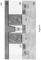
- FIG. 3 illustrates a cross sectional view of the semiconductor device shown in FIG. 2 after an etch stop layer 302 is formed over the semiconductor device in accordance with various embodiments of the present disclosure.
- the etch stop layer 302 may be deposited in the opening 202 as well as the top surface of the interlayer dielectric layer 120 .
- the etch stop layer 302 may be formed of aluminum oxynitride (AlON), aluminum oxide (Al 2 O 3 ), aluminum nitride (AlN), hafnium oxide (HfOx), zirconium oxide (ZrOx), and combinations thereof and/or the like.
- the etch stop layer 302 may be formed using suitable fabrication techniques such as CVD, although any acceptable process may be utilized to form the etch stop layer 302 to a thickness from about 10 Angstroms to about 30 Angstroms. In accordance with an embodiment, thickness of the etch stop layer 302 is approximately equal to 12 Angstroms.
- the etch stop layer 302 comprises a material different from that overlying the etch stop layer 302 .
- the material difference renders the etch rate of the etch stop layer 302 much slower than that of the material overlying it.
- the etch stop layer 302 provides a clear indicator of when to end an etching process, thereby protecting the material underlying the etch stop layer 302 .
- FIG. 4 illustrates a cross sectional view of the semiconductor device shown in FIG. 3 after a dielectric layer 402 is formed over the etch stop layer 302 in accordance with various embodiments of the present disclosure.
- the dielectric layer 402 is formed over the etch stop layer 302 .
- the dielectric layer 402 may be formed of a dielectric material such as an oxide or silicon nitride, although other suitable dielectrics, such as a high-k dielectric, may alternatively be used.
- the dielectric layer 402 may be formed using a PECVD process, although any other suitable process may alternatively be used.
- FIG. 5 illustrates a cross sectional view of the semiconductor device shown in FIG. 4 after a mask layer 502 is formed over the dielectric layer 402 in accordance with various embodiments of the present disclosure.
- the mask layer 502 is deposited over the dielectric layer 402 .
- the mask layer 502 may be made of a photoresist material.
- the mask layer 502 may be alternatively referred to as a photoresist layer 502 .
- the photoresist layer 502 may be formed by suitable techniques such as spin coating and the like.
- the photoresist material may be SU-8 (registered trademark of Shell Chemicals) photo-sensitive epoxy, film type polymer materials and/or the like. It should be noted that one skilled in the art will recognize while FIG. 5 illustrates a single photoresist layer, the photoresist layer 502 may comprise a plurality of photoresist layers.
- FIG. 6 illustrates a cross sectional view of the semiconductor device shown in FIG. 5 after an opening 602 is formed in the photoresist layer 502 in accordance with various embodiments of the present disclosure.
- selective areas of the photoresist layer 502 are exposed to light.
- a developer is applied to the photoresist layer 502 .
- the opening 602 is formed in the photoresist layer 502 .
- the outermost edge of the opening 602 is substantially aligned with the outermost edge of the opening 202 shown in FIG. 2 .
- the width of opening 602 is defined as W 3 as shown in FIG. 6 .
- photoresist layer 502 After the photoresist layer 502 is patterned, there may be two photoresist material regions formed on top of the dielectric layer 402 as shown in FIG. 6 . The remaining photoresist regions help to prevent the dielectric layer 402 underneath the photoresist layer 502 from being etched away during the etching process described below with respect to FIG. 7 .
- FIG. 7 illustrates a cross sectional view of the semiconductor device shown in FIG. 6 after an etching process is applied to the semiconductor device in accordance with various embodiments of the present disclosure.
- An etching process such as a dry etching is applied to the semiconductor device 100 .
- the exposed portion of the dielectric layer 402 is removed as a result.
- the etch stop layer 302 With the help of the etch stop layer 302 , the etching of the dielectric layer 402 is more precisely controlled.
- the etching process leads to an opening 702 over the lower drain contact 128 .
- etch stop layer 302 One advantageous feature of having the etch stop layer 302 is the high selectivity of the etch stop layer 302 helps to avoid the over-etch issue, thereby protecting the top surface of the lower drain contact 128 from being damaged when the etching process is applied to the dielectric layer 402 .
- FIG. 8 illustrates a cross sectional view of the semiconductor device shown in FIG. 7 after the remaining photoresist layer has been removed from the semiconductor device in accordance with various embodiments of the present disclosure.
- the remaining photoresist layer shown in FIG. 7 may be removed by using suitable photoresist stripping techniques such as chemical solvent cleaning, plasma ashing, dry stripping and/or the like.
- suitable photoresist stripping techniques such as chemical solvent cleaning, plasma ashing, dry stripping and/or the like.
- the photoresist stripping techniques are well known and hence are not discussed in further detail herein to avoid repetition.
- FIG. 9 illustrates a cross sectional view of the semiconductor device shown in FIG. 8 after an etching process is applied to the etch stop layer 302 in accordance with various embodiments of the present disclosure.
- the exposed etch stop layer 302 (shown in FIG. 8 ) may be removed by using a suitable etching process such as wet-etching, dry-etching and/or the like.
- the exposed etch stop layer 302 is removed by a wet etching process in which a cleaning solution is applied to the etch stop layer 302 .
- the cleaning solution is a hydrofluoric acid (HF) based cleaning solution, an aqueous ammonia (NH4OH) based cleaning solution, a Hydroxylamine based cleaning solution, any combinations thereof and the like.
- the semiconductor device 100 may be heated before and/or during the process of applying the cleaning solution to the etch stop layer 302 .
- the semiconductor device 100 is heated to about 40 degrees C.
- the time of removing the exposed etch stop layer 302 is about 30 seconds.
- the semiconductor device 100 is heated to about 60 degrees C.
- the time of removing the exposed etch stop layer 302 is about 10 seconds.
- the etching process is controlled such that portions of the protection layers 127 , 129 and the dielectric layer 402 are removed.
- a first edge 902 of the dielectric layer 402 is vertically aligned with the outermost edge of the first gate spacer 125 as indicated by the dashed line A-A′.
- a second edge 904 of the dielectric layer 402 is vertically aligned with the outermost edge of the second gate spacer 126 as indicated by the dashed line B-B′.
- the first edge 902 of the dielectric layer 402 is substantially aligned with the outermost edge of the first gate spacer 125 .
- the second edge 904 of the dielectric layer 402 is substantially aligned with the outermost edge of the second gate spacer 126 .
- the top surface of the first protection layer 127 has a first slope extending downward from an edge of the top surface of the first gate spacer 125 .
- the top surface of the second protection layer 129 has a second slope extending downward from an edge of the top surface of the second gate spacer 126 .
- the rate of change of the top surface of the first protection layer 127 is substantially equal to the rate of change of the top surface of the second protection layer 129 .
- the protection layers 127 and 129 are formed by a high temperature deposition process. As described above with respect to FIG. 2 , the protection layers 127 and 129 are formed by an ALD process and a pre-heating process is used to increase the temperature of the ALD process to a range from about 550 degrees C. to 600 degrees C. In contrast, the dielectric layer 402 is formed by a CVD process having a process temperature of about 500 degrees C.
- the different deposition process temperatures lead to different etching rates when the wet etching process is applied to the protection layers and the dielectric layer 402 . Such different etching rates help to form different surfaces at the protection layers and the dielectric layer 402 .
- an opening 901 is formed over the lower drain contact 128 .
- the opening 901 includes two portions.
- a first portion of the opening 901 has a rectangular shape.
- the first portion is in the dielectric layer 402 .
- a second portion of the opening 901 has an inverted-trapezoidal shape. As shown in FIG. 9 , the second portion of the opening 901 is in the interlayer dielectric layer 120 .
- the width of the first portion of the opening 901 is defined as W 4 . Throughout the description, W 4 is alternatively referred to as the maximum width of the opening 901 .
- W 4 is greater than W 3 as shown in FIG. 9 .
- the ratio of W 4 to W 3 is in a range from about 1.1 to about 1.3.
- FIG. 10 illustrates a cross section view of the semiconductor device shown in FIG. 9 after a metal material is filled in the opening of the semiconductor device in accordance with various embodiments of the present disclosure.
- a metallic material which includes tungsten, titanium, aluminum, copper, any combinations thereof and/or the like, is filled into the opening 901 (shown in FIG. 9 ).
- the upper drain contact 130 is formed over the lower drain contact 128 .
- the upper drain contact 130 includes an upper portion and a lower portion.
- the upper portion of the upper drain contact 130 has a rectangular shape.
- the lower portion of the upper drain contact 130 has an inverted-trapezoidal shape.
- the lower portion of the upper drain contact 130 is in contact with the first slope of the first protection layer 127 and the second slope of the second protection layer 129 .
- a first edge of the upper portion of the upper drain contact 130 is vertically aligned with an outermost edge of the first gate spacer 125 .
- a second edge of the upper portion of the upper drain contact 130 is vertically aligned with an outermost edge of the second gate spacer 126 .
- FIG. 11 illustrates a flow chart of a method for forming the semiconductor device shown in FIG. 1 in accordance with various embodiments of the present disclosure.
- This flowchart is merely an example, which should not unduly limit the scope of the claims.
- One of ordinary skill in the art would recognize many variations, alternatives, and modifications. For example, various step as illustrated in FIG. 16 may added, removed, replaced, rearranged and repeated.
- a semiconductor device comprising two transistors having a shared drain is provided.
- a lower drain contact has been formed in an interlayer dielectric layer between two gate electrodes of the two transistors.
- An opening is formed in the interlayer dielectric layer and over the lower drain contact.
- an etch stop layer is deposited in the opening and over the top surface of the interlayer dielectric layer.
- the etch stop layer is formed of formed of aluminum oxynitride (AlON), aluminum oxide (Al 2 O 3 ), aluminum nitride (AlN), hafnium oxide (HfOx), zirconium oxide (ZrOx), and combinations thereof and/or the like.
- a dielectric layer is formed over the etch stop layer.
- the dielectric layer is formed of silicon nitride.
- the dielectric layer is in the opening and over the interlayer dielectric layer.
- a photoresist layer is deposited over the dielectric layer.
- the photoresist layer is exposed to light according to a predetermined pattern.
- an opening is formed in the photoresist layer by applying a developer to the photoresist layer.
- an etching process is applied to the dielectric layer until the etch stop layer is exposed.
- the remaining photoresist layer is removed by a suitable photoresist removal process.
- the exposed etch stop layer is removed by a suitable etching process.
- the etching process is controlled such that a first edge of the dielectric layer is vertically aligned with a spacer sidewall of a first transistor; a second edge of the dielectric layer is vertically aligned with a spacer sidewall of a second transistor; a top surface of a first protection layer has a slope extending downward from an edge of a top surface of a first gate spacer of the first transistor; a top surface of a second protection layer has a slope extending downward from an edge of a top surface of a second gate spacer of the second transistor.
- a conductive material is filled in the opening to form an upper drain contact.
- the upper drain contact is on and in contact with the lower drain contact.
- FIG. 12 illustrates a cross sectional view of a FinFET semiconductor device having an enlarged drain/source contact in accordance with various embodiments of the present disclosure.
- the drain contact fabrication process shown in FIGS. 2-11 is applied not only to planar transistor devices, but also to FinFET devices.
- the FinFET semiconductor device 1200 comprises two transistors sharing a common drain. These two transistors are formed over a substrate 104 .
- a first transistor 101 comprises a first gate electrode 123 and its gate dielectric layer 121 , a drain 114 and its contacts 128 and 130 , and a first source 112 and its contact (not shown).
- a second transistor 102 comprises a second gate electrode 124 and its gate dielectric layer 122 , the drain 114 and its contacts 128 and 130 , and a second source 116 and its contact (not shown).
- the drain/source regions 112 , 114 and 116 may be formed by etching portions of a fin line and growing the drain/source regions 112 , 114 and 116 through suitable epitaxial growth processes. As shown in FIG. 12 , the top surfaces of the drain/source regions 112 , 114 and 116 are higher than the bottom surfaces of the gate electrodes 123 and 124 .
- the shape of the upper drain contact 130 in FIG. 12 is similar to that shown in FIG. 1 , and hence is not discussed in detail to avoid unnecessary repetition.
- One advantageous feature of having the enlarged drain contact 130 shown in FIG. 12 is the enlarged drain contact helps to reduce the contact resistance, thereby improving the performance of FinFET semiconductor device 1200 .
- an apparatus comprises a first source and a common drain in a substrate and on opposite sides of a first gate, the first gate being surrounded by a first gate spacer, a second source and the common drain in the substrate and on opposite sides of a second gate, the second gate being surrounded by a second gate spacer, a first protection layer formed along a sidewall of the first gate spacer, wherein a top surface of the first protection layer has a first slope, a second protection layer formed along a sidewall of the second gate spacer, wherein a top surface of the second protection layer has a second slope, a lower drain contact between the first gate and the second gate and an upper drain contact over the lower drain contact and between the first gate and the second gate, wherein at least a portion of the upper drain contact is in contact with the first slope and the second slope.
- a device comprises a first drain/source region and a second drain/source region in a substrate and on opposite sides of a first gate, wherein the second drain/source region and the first gate are separated by a first gate spacer, a third drain/source region and the second drain/source region in the substrate and on opposite sides of a second gate, wherein the second drain/source region and the second gate are separated by a second gate spacer, a first protection layer formed along a sidewall of the first gate spacer, wherein the first protection layer is over the second drain/source region, a second protection layer formed along a sidewall of the second gate spacer, wherein the second protection layer is over the second drain/source region, a lower drain contact between the first protection layer and the second protection layer and an upper drain contact over the lower drain contact and between the first gate and the second gate, wherein a width of the upper drain contact is greater than a width of the lower drain contact.
- an apparatus comprises a first source and a common drain on opposite sides of a first gate, a second source and the common drain on opposite sides of a second gate, wherein the first gate and the second gate are in an interlayer dielectric layer over a substrate and the first gate and the second gate are surrounded by a first gate spacer and a second gate spacer respectively.
- the apparatus further comprises a first protection layer formed along a sidewall of the first gate spacer, wherein the first protection layer is over the common drain and a top surface of the first protection layer has a first slope, a second protection layer formed along a sidewall of the second gate spacer, wherein the second protection layer is over the common drain and a top surface of the second protection layer has a second slope and a first drain contact formed between the first gate and the second gate, wherein a width of an upper portion of the first drain contact is greater than a width of a lower portion of the first drain contact.
Abstract
An apparatus includes a first source and a common drain and on opposite sides of a first gate surrounded by a first gate spacer, a second source and the common drain on opposite sides of a second gate surrounded by a second gate spacer, a first protection layer formed along a sidewall of the first gate spacer, wherein a top surface of the first protection layer has a first slope, a second protection layer formed along a sidewall of the second gate spacer, wherein a top surface of the second protection layer has a second slope, a lower drain contact between the first gate and the second gate and an upper drain contact over the lower drain contact and between the first gate and the second gate, wherein at least a portion of the upper drain contact is in contact with the first slope and the second slope.
Description
This application is a continuation of U.S. application Ser. No. 16/016,962, filed on Jun. 25, 2018, now U.S. Pat. No. 10,770,356 issued Sep. 8, 2020, entitled “Contact Structure and Method of Fabricating the Same,” which is a divisional of U.S. application Ser. No. 15/364,136, filed on Nov. 29, 2016, now U.S. Pat. No. 10,037,918 issued Jul. 31, 2018, entitled “Contact Structure and Method of Fabricating the Same,” which application is hereby incorporated herein by reference.
The semiconductor industry has experienced rapid growth due to continuous improvements in the integration density of a variety of electronic components (e.g., transistors, diodes, resistors, capacitors, etc.). For the most part, this improvement in integration density has come from repeated reductions in minimum feature size, which allows more components to be integrated into a given area. However, the smaller feature size may lead to the undesirable increase in contact resistance. As the demand for miniaturization, higher speed and greater bandwidth, as well as lower power consumption and latency has grown recently, there has grown a need for reducing contact resistance.
Aspects of the present disclosure are best understood from the following detailed description when read with the accompanying figures. It is noted that, in accordance with the standard practice in the industry, various features are not drawn to scale. In fact, the dimensions of the various features may be arbitrarily increased or reduced for clarity of discussion.
The following disclosure provides many different embodiments, or examples, for implementing different features of the invention. Specific examples of components and arrangements are described below to simplify the present disclosure. These are, of course, merely examples and are not intended to be limiting. For example, the formation of a first feature over or on a second feature in the description that follows may include embodiments in which the first and second features are formed in direct contact, and may also include embodiments in which additional features may be formed between the first and second features, such that the first and second features may not be in direct contact. In addition, the present disclosure may repeat reference numerals and/or letters in the various examples. This repetition is for the purpose of simplicity and clarity and does not in itself dictate a relationship between the various embodiments and/or configurations discussed.
Further, spatially relative terms, such as “beneath,” “below,” “lower,” “above,” “upper” and the like, may be used herein for ease of description to describe one element or feature's relationship to another element(s) or feature(s) as illustrated in the figures. The spatially relative terms are intended to encompass different orientations of the device in use or operation in addition to the orientation depicted in the figures. The apparatus may be otherwise oriented (rotated 90 degrees or at other orientations) and the spatially relative descriptors used herein may likewise be interpreted accordingly.
The present disclosure will be described with respect to embodiments in a specific context, a drain contact structure having an enlarged top critical dimension and a method of forming the same. The embodiments of the disclosure may also be applied, however, to a variety of semiconductor structures. For example, the fabrication process may be applicable to forming a source contact structure. Furthermore, the embodiments of the disclosure are applicable to not only planar transistor devices, but also to fin field effect transistor (FinFET) devices. Hereinafter, various embodiments will be explained in detail with reference to the accompanying drawings.
It should be noted that the common drain structure shown in FIG. 1 is selected purely for demonstration purposes and is not intended to limit the various embodiments of the present disclosure. One of ordinary skill in the art would recognize many variations, alternatives, and modifications. For example, the semiconductor device 100 may comprise two transistors sharing a common source.
As shown in FIG. 1 , a first gate spacer 125 is formed immediately adjacent to the first gate electrode 123. The first gate spacer 125 includes two portions from the cross sectional view shown in FIG. 1 . A first portion is formed on one side of the first gate electrode 123. A second portion is formed on an opposite side of the first gate electrode 123. The first source 112 and the first gate electrode 123 are separated by the first portion of the first gate spacer 125. The drain 114 and the first gate electrode 123 are separated by the second portion of the first gate spacer 125.
A second gate spacer 126 is formed immediately adjacent to the second gate electrode 124. Likewise, the second source 116 and the second gate electrode 124 are separated by the second gate spacer 126.
The gate electrodes 123 and 124 are formed in an interlayer dielectric layer 120. An etch stop layer 302 is formed over the interlayer dielectric layer 120. A dielectric layer 402 is formed over the etch stop layer 302. Drain contacts 128 and 130 are formed between the first gate electrode 123 and the second gate electrode 124.
The drain contact 128 is embedded in the interlayer dielectric layer 120 and between the first gate electrode 123 and the second gate electrode 124. A bottom surface of the drain contact 128 is contact with the drain 114. It should be noted that a silicide region (not shown) may be formed between the drain 114 and the drain contact 128 to improve the contact resistance of the drain 114. Throughout the description, the drain contact 128 is alternatively referred to as a lower drain contact 128.
In some embodiments, the lower drain contact 128 has an inverted-trapezoidal shape as shown in FIG. 1 . The shape of the lower drain contact 128 shown in FIG. 1 is merely an example. A person skilled in the art would understand the lower drain contact 128 may comprise other shapes, such as, but not limited to rectangular, square, trapezoidal and the like.
As shown in FIG. 1 , the drain contact 130 is stacked on the drain contact 128. Throughout the description, the drain contact 130 is alternatively referred to as an upper drain contact 130. A lower portion of the upper drain contact 130 is inverted-trapezoidal in shape and between the first gate electrode 123 and the second gate electrode 124. An upper portion of the drain contact 130 is rectangular in shape and extends through the dielectric layer 402 and the etch stop layer 302.
As shown in FIG. 1 , the width of the bottom of the upper drain contact 130 is approximately equal to the width of the top of the lower drain contact 128. A middle portion of the upper drain contact 130 is adjacent to the first gate spacer 125 and the second gate spacer 126. In order to protect the sidewalls of the gate spacers as well as the gate electrodes 123 and 124, a first protection layer 127 is formed between the drain contacts and the first gate spacer 125. A second protection layer 129 is formed between the drain contacts and the second gate spacer 126.
It should be noted that while FIG. 1 illustrates two separate protection layers 127 and 129 from the cross sectional view of the semiconductor device 100, one of ordinary skill in the art would recognize many variations, alternatives, and modifications. For example, in some embodiments, the protection layers 127 and 129 may be portions of a continuous protection layer.
As shown in FIG. 1 , the top surface of the first protection layer 127 has a slope extending downward from an edge of a top surface of the first gate spacer 125. Likewise, the top surface of the second protection layer 129 has a slope extending downward from an edge of a top surface of the second gate spacer 126. The slopes of the protection layers 127 and 129 help to increase the size of the trench where the upper drain contact 130 is formed, thereby improving the metal gap fill of the drain contacts. As shown in FIG. 1 , the width of the trench has been increased from W2 to W1. W2 is the minimum distance between the first protection layer 127 and the second protection layer 129. W1 is the width of the upper portion of the upper drain contact 130. In some embodiments, the ratio of W1 to W2 is in a range from about 1.1 to about 1.3.
One advantageous feature of having the enlarged trench shown in FIG. 1 is the enlarged trench helps to reduce the contact resistance, thereby improving the performance of the semiconductor device 100. For example, the resistive-capacitive (R-C) delay of the semiconductor device 100 may be improved through the enlarged drain contact 130 as shown in FIG. 1 . The detailed process of forming the upper drain contact 130, and the protection layers 127 and 129 will be described below with respect to FIGS. 2-10
The substrate 104 may be formed of silicon, although it may also be formed of other group III, group IV, and/or group V elements, such as silicon, germanium, gallium, arsenic, and combinations thereof. The substrate 104 may also be in the form of silicon-on-insulator (SOI). The SOI substrate may comprise a layer of a semiconductor material (e.g., silicon, germanium and/or the like) formed over an insulator layer (e.g., buried oxide or the like), which is formed in a silicon substrate. In addition, other substrates that may be used include multi-layered substrates, gradient substrates, hybrid orientation substrates and/or the like.
The substrate 104 may further comprise a variety of electrical circuits such as transistors (e.g., transistor 101 and transistor 102). For simplicity, only two transistors having a shared drain are presented to illustrate the innovative aspects of various embodiments.
The electrical circuits formed on the substrate 104 may be any type of circuitry suitable for a particular application. In accordance with an embodiment, the electrical circuits may include various n-type metal-oxide semiconductor (NMOS) and/or p-type metal-oxide semiconductor (PMOS) devices such as transistors, capacitors, resistors, diodes, photo-diodes, fuses and the like. The electrical circuits may be interconnected to perform one or more functions. The functions may include memory structures, processing structures, sensors, amplifiers, power distribution, input/output circuitry or the like.
In accordance with an embodiment, the substrate 104 may be a p substrate, which is doped with a p-type impurity such as boron, indium or the like. Depending on design needs and different applications, a p-type epitaxial layer (not shown) may be grown from the p-type substrate 104. The sources 112, 116 and drain 114 may be formed in the p-type epitaxial layer. The epitaxial growth of the p-type epitaxial layer may be implemented by using suitable semiconductor fabrication processes such as chemical vapor deposition (CVD), ultra-high vacuum chemical vapor deposition (UHV-CVD) and the like.
As shown in FIG. 2 , the first source 112 and the drain 114 are formed on opposing sides of the first gate electrode 123. The second source 116 and the drain 114 are formed on opposing sides of the second gate electrode 124. In an embodiment in which the substrate 104 is an n-type substrate, the drain and source regions may be formed by implanting appropriate p-type dopants such as boron, gallium, indium and/or the like. Alternatively, in an embodiment in which the substrate 104 is a p-type substrate, the drain and source regions may be formed by implanting appropriate n-type dopants such as phosphorous, arsenic and/or the like.
The isolation regions 106 and 108 may be shallow trench isolation (STI) regions, and may be formed by etching the substrate 104 to form a plurality of trenches and filling the trenches with a dielectric material as is known in the art. For example, the isolation regions 106 and 108 may be filled with a dielectric material such as an oxide material, a high-density plasma (HDP) oxide and/or the like. A planarization process such as a chemical mechanical polish (CMP) process may be applied to the top surface so that the excess dielectric material may be removed as a result.
The gate dielectric layers 121 and 122 may be formed of a dielectric material such as silicon oxide, silicon oxynitride, silicon nitride, an oxide, a nitrogen-containing oxide, a combination thereof and/or the like. The gate dielectric layers 121 and 122 may have a relative permittivity value greater than about 4. Other examples of such materials include aluminum oxide, lanthanum oxide, hafnium oxide, zirconium oxide, hafnium oxynitride, combinations thereof and/or the like. In an embodiment in which the gate dielectric layers 121 and 122 comprise an oxide layer, the gate dielectric layers 121 and 122 may be formed by a plasma enhanced CVD (PECVD) process using tetraethoxysilane (TEOS) and oxygen as a precursor. In accordance with an embodiment, the gate dielectric layers 121 and 122 may be of a thickness in a range from about 8 Angstroms to about 200 Angstroms.
The gate electrodes 123 and 124 may comprise a conductive material, such as a metal (e.g., tantalum, titanium, molybdenum, tungsten, platinum, aluminum, hafnium, ruthenium), a metal silicide (e.g., titanium silicide, cobalt silicide, nickel silicide, tantalum silicide), a metal nitride (e.g., titanium nitride, tantalum nitride), doped poly-crystalline silicon, other conductive materials, combinations thereof and/or the like. In an embodiment in which the gate electrodes 123 and 124 are formed of poly-silicon, the gate electrodes 123 and 124 may be formed by depositing doped or undoped poly-silicon by low-pressure chemical vapor deposition (LPCVD). Throughout the description, the gate electrodes 123 and 124 may be alternatively referred to as the first gate 123 and the second gate 124 respectively.
The gate spacers 125 and 126 may be formed by blanket depositing one or more spacer layers (not shown) over the gates 123, 124 and the substrate 104 and etching the spacer layers to form the gate spacers 125 and 126. The gate spacers 125 and 126 may comprise suitable dielectric materials such as SiN, oxynitride, SiC, SiON, oxide and/or the like. The gate spacers 125 and 126 may be formed by commonly used techniques such as CVD, PECVD, sputter and/or the like.
A first protection layer 127 is formed along the sidewall of the first gate spacer 125 and a second protection layer 129 is formed along the sidewall of the second gate spacer 126. In some embodiments, the first protection layer 127 and the second protection layer 129 may function as contact etch stop layers (CESL). The CESL layers may comprise commonly used dielectric materials, such as silicon nitride, silicon oxynitride, silicon oxycarbide, silicon carbide, combinations thereof, and multi-layers thereof. In some embodiments, besides stopping an etching process, the CESL layers also apply a stress to the channel regions of the respective transistors.
In some embodiments, the first protection layer 127 and the second protection layer 129 are portions of a continuous protection layer. The continuous protection layer is formed by depositing a dielectric layer through an atomic layer deposition (ALD) process and etching the dielectric layer to form the protection layers shown in FIG. 2 . Prior to performing the ALD process on the semiconductor process 100, a pre-heating process is applied to the semiconductor device 100. The pre-heating process is employed to increase the temperature of the ALD process to a higher temperature. In some embodiments, after applying the pre-heating process to the semiconductor process 100, the temperature of the ALD process is in a range from about 550 degrees Celsius (C) to about 600 degrees C.
As shown in FIG. 2 , the interlayer dielectric layer 120 is formed over the substrate 104. The interlayer dielectric layer 120 may be formed, for example, of a low-K dielectric material, such as silicon oxide. The interlayer dielectric layer 120 may be formed by any suitable method known in the art, such as spinning, CVD, PECVD and the like. It should also be noted that one skilled in the art will recognize while FIG. 2 illustrates a single interlayer dielectric layer, the interlayer dielectric layer 120 may comprise a plurality of dielectric layers.
In some embodiments, the interlayer dielectric layer 120 may comprise a lower portion and an upper portion. The lower portion and the upper portion of interlayer dielectric layer 120 are formed by two separate fabrication steps. After the lower portion has been formed, the lower drain contact 128 is formed in the lower portion of the interlayer dielectric layer 120 and between the first gate 123 and the second gate 124. The lower drain contact 128 is used to provide an electrical connection between the drain 114 and the interconnect structure (not shown) formed over the interlayer dielectric layer 120.
The lower drain contact 128 may be formed by using photolithography techniques to deposit and pattern a photoresist material on the lower portion of the interlayer dielectric layer 120. A portion of the photoresist is exposed according to the location and shape of the lower drain contact 128. An etching process, such as an anisotropic dry etch process, may be used to create an opening in the lower portion of the interlayer dielectric layer 120. A conductive liner (not shown) may be deposited prior to filling the contact opening. In some embodiments, the conductive liner is conformal, and may comprise a single layer of Ta, TaN, WN, WSi, TiN, Ru and combinations thereof. The conductive liner may be used as a barrier layer for preventing the conductive material such as copper from diffusing into the underlying substrate 104. The conductive liner may be deposited by using suitable deposition processes such as CVD, PVD, ALD and/or the like.
A conductive material is then filled in the opening. The conductive material may be deposited by using suitable deposition processes such as CVD, PVD, ALD and the like. The conductive material is deposited over the conductive liner to fill the contact opening. The conductive material may be copper, tungsten, aluminum, silver, titanium, titanium nitride, tantalum and combinations thereof and/or the like.
It should be noted a plurality of silicide regions may be formed on the top surfaces of the drain and source regions. The silicide regions may be formed by a salicide process, on the respective source/drain regions. As is known in the art, in the salicide process for forming silicide regions, a metal layer is formed by first depositing a thin layer of metal, such as cobalt, nickel, titanium, and the like, over the device. The device is then annealed to form silicide regions between the deposited metal and the underlying exposed silicon regions.
It should be noted that the gate electrodes 123 and 124 shown in FIG. 2 may be formed by a gate-last semiconductor fabrication process. More particularly, a dielectric layer (e.g., silicon oxide) and a dummy gate layer (e.g., polycrystalline silicon) are deposited over the substrate 104. Two gate stack structures are formed by etching the dielectric layer and the dummy gate layer. A dielectric material (e.g., silicon nitride) is deposited and etched to from the gate spacers 125 and 126. Then an interlayer dielectric layer (e.g., layer 120) is deposited over the substrate 104. The dummy gate layer and the dielectric layer are removed by suitable etching processes to form two gate trenches. The gate trenches are filled with a high-k dielectric material to form the gate dielectric layers 121 and 122, and a gate material to form the gate electrodes 123 and 124 as shown in FIG. 2 .
The etch stop layer 302 may be formed using suitable fabrication techniques such as CVD, although any acceptable process may be utilized to form the etch stop layer 302 to a thickness from about 10 Angstroms to about 30 Angstroms. In accordance with an embodiment, thickness of the etch stop layer 302 is approximately equal to 12 Angstroms.
In some embodiments, the etch stop layer 302 comprises a material different from that overlying the etch stop layer 302. The material difference renders the etch rate of the etch stop layer 302 much slower than that of the material overlying it. The etch stop layer 302 provides a clear indicator of when to end an etching process, thereby protecting the material underlying the etch stop layer 302.
The photoresist layer 502 may be formed by suitable techniques such as spin coating and the like. The photoresist material may be SU-8 (registered trademark of Shell Chemicals) photo-sensitive epoxy, film type polymer materials and/or the like. It should be noted that one skilled in the art will recognize while FIG. 5 illustrates a single photoresist layer, the photoresist layer 502 may comprise a plurality of photoresist layers.
In some embodiments, the outermost edge of the opening 602 is substantially aligned with the outermost edge of the opening 202 shown in FIG. 2 . The width of opening 602 is defined as W3 as shown in FIG. 6 .
After the photoresist layer 502 is patterned, there may be two photoresist material regions formed on top of the dielectric layer 402 as shown in FIG. 6 . The remaining photoresist regions help to prevent the dielectric layer 402 underneath the photoresist layer 502 from being etched away during the etching process described below with respect to FIG. 7 .
One advantageous feature of having the etch stop layer 302 is the high selectivity of the etch stop layer 302 helps to avoid the over-etch issue, thereby protecting the top surface of the lower drain contact 128 from being damaged when the etching process is applied to the dielectric layer 402.
In some embodiments, the exposed etch stop layer 302 is removed by a wet etching process in which a cleaning solution is applied to the etch stop layer 302. In some embodiments, the cleaning solution is a hydrofluoric acid (HF) based cleaning solution, an aqueous ammonia (NH4OH) based cleaning solution, a Hydroxylamine based cleaning solution, any combinations thereof and the like.
The semiconductor device 100 may be heated before and/or during the process of applying the cleaning solution to the etch stop layer 302. In an embodiment, the semiconductor device 100 is heated to about 40 degrees C. The time of removing the exposed etch stop layer 302 is about 30 seconds. In an alternative embodiment, the semiconductor device 100 is heated to about 60 degrees C. The time of removing the exposed etch stop layer 302 is about 10 seconds.
In order to have an enlarged opening, the etching process is controlled such that portions of the protection layers 127, 129 and the dielectric layer 402 are removed. In particular, after the etching process finishes, a first edge 902 of the dielectric layer 402 is vertically aligned with the outermost edge of the first gate spacer 125 as indicated by the dashed line A-A′. Likewise, a second edge 904 of the dielectric layer 402 is vertically aligned with the outermost edge of the second gate spacer 126 as indicated by the dashed line B-B′. In an alternative embodiment, the first edge 902 of the dielectric layer 402 is substantially aligned with the outermost edge of the first gate spacer 125. The second edge 904 of the dielectric layer 402 is substantially aligned with the outermost edge of the second gate spacer 126.
Furthermore, the top surface of the first protection layer 127 has a first slope extending downward from an edge of the top surface of the first gate spacer 125. The top surface of the second protection layer 129 has a second slope extending downward from an edge of the top surface of the second gate spacer 126. As shown in FIG. 9 , the rate of change of the top surface of the first protection layer 127 is substantially equal to the rate of change of the top surface of the second protection layer 129.
It should be noted that the protection layers 127 and 129 are formed by a high temperature deposition process. As described above with respect to FIG. 2 , the protection layers 127 and 129 are formed by an ALD process and a pre-heating process is used to increase the temperature of the ALD process to a range from about 550 degrees C. to 600 degrees C. In contrast, the dielectric layer 402 is formed by a CVD process having a process temperature of about 500 degrees C. The different deposition process temperatures lead to different etching rates when the wet etching process is applied to the protection layers and the dielectric layer 402. Such different etching rates help to form different surfaces at the protection layers and the dielectric layer 402.
After the etching process finishes, an opening 901 is formed over the lower drain contact 128. The opening 901 includes two portions. A first portion of the opening 901 has a rectangular shape. The first portion is in the dielectric layer 402. A second portion of the opening 901 has an inverted-trapezoidal shape. As shown in FIG. 9 , the second portion of the opening 901 is in the interlayer dielectric layer 120. The width of the first portion of the opening 901 is defined as W4. Throughout the description, W4 is alternatively referred to as the maximum width of the opening 901.
As shown in FIG. 9 , portions of the dielectric layer 402 have been removed during the etching process. The sidewalls of the dielectric layer 402 are aligned with the sidewalls of the gate spacers 125 and 126 respectively. As such, W4 is greater than W3 as shown in FIG. 9 . In some embodiments, the ratio of W4 to W3 is in a range from about 1.1 to about 1.3.
As shown in FIG. 10 , the upper drain contact 130 includes an upper portion and a lower portion. The upper portion of the upper drain contact 130 has a rectangular shape. The lower portion of the upper drain contact 130 has an inverted-trapezoidal shape. Furthermore, the lower portion of the upper drain contact 130 is in contact with the first slope of the first protection layer 127 and the second slope of the second protection layer 129. A first edge of the upper portion of the upper drain contact 130 is vertically aligned with an outermost edge of the first gate spacer 125. A second edge of the upper portion of the upper drain contact 130 is vertically aligned with an outermost edge of the second gate spacer 126.
At step 1102, a semiconductor device comprising two transistors having a shared drain is provided. A lower drain contact has been formed in an interlayer dielectric layer between two gate electrodes of the two transistors. An opening is formed in the interlayer dielectric layer and over the lower drain contact.
At step 1104, an etch stop layer is deposited in the opening and over the top surface of the interlayer dielectric layer. The etch stop layer is formed of formed of aluminum oxynitride (AlON), aluminum oxide (Al2O3), aluminum nitride (AlN), hafnium oxide (HfOx), zirconium oxide (ZrOx), and combinations thereof and/or the like.
At step 1106, a dielectric layer is formed over the etch stop layer. The dielectric layer is formed of silicon nitride. The dielectric layer is in the opening and over the interlayer dielectric layer.
At step 1108, a photoresist layer is deposited over the dielectric layer. At step 1110, the photoresist layer is exposed to light according to a predetermined pattern. At step 1112, an opening is formed in the photoresist layer by applying a developer to the photoresist layer.
At step 1114, an etching process is applied to the dielectric layer until the etch stop layer is exposed. At step 1116, the remaining photoresist layer is removed by a suitable photoresist removal process.
At step 1118, the exposed etch stop layer is removed by a suitable etching process. During the process of removing the etch stop layer, the upper portions of the protection layers and portions of the dielectric layer have been removed. In particular, the etching process is controlled such that a first edge of the dielectric layer is vertically aligned with a spacer sidewall of a first transistor; a second edge of the dielectric layer is vertically aligned with a spacer sidewall of a second transistor; a top surface of a first protection layer has a slope extending downward from an edge of a top surface of a first gate spacer of the first transistor; a top surface of a second protection layer has a slope extending downward from an edge of a top surface of a second gate spacer of the second transistor.
At step 1120, through a plating process, a conductive material is filled in the opening to form an upper drain contact. The upper drain contact is on and in contact with the lower drain contact.
The drain/ source regions 112, 114 and 116 may be formed by etching portions of a fin line and growing the drain/ source regions 112, 114 and 116 through suitable epitaxial growth processes. As shown in FIG. 12 , the top surfaces of the drain/ source regions 112, 114 and 116 are higher than the bottom surfaces of the gate electrodes 123 and 124.
The shape of the upper drain contact 130 in FIG. 12 is similar to that shown in FIG. 1 , and hence is not discussed in detail to avoid unnecessary repetition. One advantageous feature of having the enlarged drain contact 130 shown in FIG. 12 is the enlarged drain contact helps to reduce the contact resistance, thereby improving the performance of FinFET semiconductor device 1200.
In accordance with an embodiment, an apparatus comprises a first source and a common drain in a substrate and on opposite sides of a first gate, the first gate being surrounded by a first gate spacer, a second source and the common drain in the substrate and on opposite sides of a second gate, the second gate being surrounded by a second gate spacer, a first protection layer formed along a sidewall of the first gate spacer, wherein a top surface of the first protection layer has a first slope, a second protection layer formed along a sidewall of the second gate spacer, wherein a top surface of the second protection layer has a second slope, a lower drain contact between the first gate and the second gate and an upper drain contact over the lower drain contact and between the first gate and the second gate, wherein at least a portion of the upper drain contact is in contact with the first slope and the second slope.
In accordance with an embodiment, a device comprises a first drain/source region and a second drain/source region in a substrate and on opposite sides of a first gate, wherein the second drain/source region and the first gate are separated by a first gate spacer, a third drain/source region and the second drain/source region in the substrate and on opposite sides of a second gate, wherein the second drain/source region and the second gate are separated by a second gate spacer, a first protection layer formed along a sidewall of the first gate spacer, wherein the first protection layer is over the second drain/source region, a second protection layer formed along a sidewall of the second gate spacer, wherein the second protection layer is over the second drain/source region, a lower drain contact between the first protection layer and the second protection layer and an upper drain contact over the lower drain contact and between the first gate and the second gate, wherein a width of the upper drain contact is greater than a width of the lower drain contact.
In accordance with an embodiment, an apparatus comprises a first source and a common drain on opposite sides of a first gate, a second source and the common drain on opposite sides of a second gate, wherein the first gate and the second gate are in an interlayer dielectric layer over a substrate and the first gate and the second gate are surrounded by a first gate spacer and a second gate spacer respectively.
The apparatus further comprises a first protection layer formed along a sidewall of the first gate spacer, wherein the first protection layer is over the common drain and a top surface of the first protection layer has a first slope, a second protection layer formed along a sidewall of the second gate spacer, wherein the second protection layer is over the common drain and a top surface of the second protection layer has a second slope and a first drain contact formed between the first gate and the second gate, wherein a width of an upper portion of the first drain contact is greater than a width of a lower portion of the first drain contact.
The foregoing outlines features of several embodiments so that those skilled in the art may better understand the aspects of the present disclosure. Those skilled in the art should appreciate that they may readily use the present disclosure as a basis for designing or modifying other processes and structures for carrying out the same purposes and/or achieving the same advantages of the embodiments introduced herein. Those skilled in the art should also realize that such equivalent constructions do not depart from the spirit and scope of the present disclosure, and that they may make various changes, substitutions, and alterations herein without departing from the spirit and scope of the present disclosure.
Claims (20)
1. A method comprising:
forming a first dielectric layer over a substrate;
forming a first opening in the first dielectric layer to expose a conductive feature;
depositing an etch stop layer in the first opening and on a top surface of the first dielectric layer;
depositing a second dielectric layer over the etch stop layer;
depositing a photoresist layer on the second dielectric layer;
patterning the photoresist layer to form a second opening in the photoresist layer;
applying a first etching process to the second dielectric layer to form a third opening in the second dielectric layer, the third opening exposing the etch stop layer;
performing a second etching process on the etch stop layer to form a fourth opening, the fourth opening exposing the conductive feature, a width of the fourth opening in the second dielectric layer being greater than a width of the third opening in the second dielectric layer; and
filling the fourth opening with a conductive material.
2. The method of claim 1 , wherein the conductive feature comprises a source/drain contact.
3. The method of claim 2 , wherein the source/drain contact is interposed between a first gate electrode and a second gate electrode.
4. The method of claim 3 , wherein the conductive material extends lower than an upper surface of the first gate electrode and the second gate electrode.
5. The method of claim 3 , wherein a third dielectric layer extends along a sidewall of the first gate electrode and a fourth dielectric layer extends along a sidewall of the third dielectric layer, the third dielectric layer being interposed between the first gate electrode and the fourth dielectric layer, wherein performing the second etching process comprises removing portions of the fourth dielectric layer.
6. The method of claim 1 , wherein an outermost edge of the second opening is aligned with an outermost edge of the first opening.
7. The method of claim 1 , wherein the etch stop layer comprises aluminum oxynitride, aluminum oxide, aluminum nitride, hafnium oxide, or zirconium oxide.
8. A method comprising:
forming a first opening in a first dielectric layer, wherein the first opening exposes a conductive feature;
depositing an etch stop layer on the conductive feature in the first opening and over an upper surface of the first dielectric layer;
depositing a second dielectric layer over the etch stop layer in the first opening and over the upper surface of the first dielectric layer;
performing a first etching process to form a second opening in the second dielectric layer, the second opening exposing the etch stop layer in the first opening;
performing a second etching process to widen the second opening and extend through the etch stop layer, thereby forming a third opening; and
filling the third opening with a conductive material.
9. The method of claim 8 further comprising:
forming a first transistor and a second transistor over a substrate, wherein:
the first transistor comprises a first gate structure; and
the second transistor comprises a second gate structure, the first transistor and the second transistor having a shared source/drain; and
forming a first dielectric layer adjacent the first gate structure and the second gate structure, wherein performing the second etching process removes portions of the first dielectric layer.
10. The method of claim 9 , wherein the conductive material completely covers an upper surface of the first dielectric layer in a cross-sectional view.
11. The method of claim 9 further comprising:
forming a second dielectric layer adjacent the first gate structure and the second gate structure, wherein the second dielectric layer is interposed between the first gate structure and the first dielectric layer and between the second gate structure and the first dielectric layer, wherein second etching process does not thin the second dielectric layer.
12. The method of claim 11 , wherein the conductive material extends along sidewalls of the second dielectric layer.
13. The method of claim 8 , wherein the etch stop layer comprises aluminum oxynitride, aluminum oxide, aluminum nitride, hafnium oxide, or zirconium oxide.
14. The method of claim 8 , wherein sidewalls of the conductive feature have a first slope, sidewalls of the conductive material have a second slope different than the first slope.
15. The method of claim 8 , wherein a sidewall of the conductive material in the second dielectric layer has a first slope, a sidewall of the conductive material below the second dielectric layer has a second slope different than the first slope.
16. A method comprising:
forming a first trench in a first dielectric layer, wherein a bottom of the first trench comprises a conductive feature;
depositing an etch stop layer in the first trench, the etch stop layer extending over the conductive feature;
depositing a second dielectric layer over the etch stop layer in the first trench;
performing a first etching process to remove the second dielectric layer in the first trench;
performing a second etching process to remove the etch stop layer in the first trench and expose the conductive feature; and
forming a conductive material over the conductive feature.
17. The method of claim 16 , wherein the second etching process widens the first trench.
18. The method of claim 16 , wherein the first dielectric layer comprises a third dielectric layer and a fourth dielectric layer, wherein after forming the etch stop layer the third dielectric layer is interposed between the etch stop layer and the fourth dielectric layer.
19. The method of claim 18 , wherein the second etching process removes portions of the fourth dielectric layer.
20. The method of claim 18 , wherein the conductive material extends completely over an upper surface of the third dielectric layer and an upper surface of the fourth dielectric layer from the conductive feature to a distal sidewall of the fourth dielectric layer from the conductive feature in a cross-sectional view.
Priority Applications (1)
| Application Number | Priority Date | Filing Date | Title |
|---|---|---|---|
| US17/010,995 US11282750B2 (en) | 2016-11-29 | 2020-09-03 | Contact structure and method of fabricating the same |
Applications Claiming Priority (3)
| Application Number | Priority Date | Filing Date | Title |
|---|---|---|---|
| US15/364,136 US10037918B2 (en) | 2016-11-29 | 2016-11-29 | Contact structure and method of fabricating the same |
| US16/016,962 US10770356B2 (en) | 2016-11-29 | 2018-06-25 | Contact structure and method of fabricating the same |
| US17/010,995 US11282750B2 (en) | 2016-11-29 | 2020-09-03 | Contact structure and method of fabricating the same |
Related Parent Applications (1)
| Application Number | Title | Priority Date | Filing Date |
|---|---|---|---|
| US16/016,962 Continuation US10770356B2 (en) | 2016-11-29 | 2018-06-25 | Contact structure and method of fabricating the same |
Publications (2)
| Publication Number | Publication Date |
|---|---|
| US20200402859A1 US20200402859A1 (en) | 2020-12-24 |
| US11282750B2 true US11282750B2 (en) | 2022-03-22 |
Family
ID=62190473
Family Applications (3)
| Application Number | Title | Priority Date | Filing Date |
|---|---|---|---|
| US15/364,136 Active 2036-12-05 US10037918B2 (en) | 2016-11-29 | 2016-11-29 | Contact structure and method of fabricating the same |
| US16/016,962 Active 2037-02-22 US10770356B2 (en) | 2016-11-29 | 2018-06-25 | Contact structure and method of fabricating the same |
| US17/010,995 Active US11282750B2 (en) | 2016-11-29 | 2020-09-03 | Contact structure and method of fabricating the same |
Family Applications Before (2)
| Application Number | Title | Priority Date | Filing Date |
|---|---|---|---|
| US15/364,136 Active 2036-12-05 US10037918B2 (en) | 2016-11-29 | 2016-11-29 | Contact structure and method of fabricating the same |
| US16/016,962 Active 2037-02-22 US10770356B2 (en) | 2016-11-29 | 2018-06-25 | Contact structure and method of fabricating the same |
Country Status (3)
| Country | Link |
|---|---|
| US (3) | US10037918B2 (en) |
| CN (1) | CN108122845B (en) |
| TW (1) | TWI745375B (en) |
Families Citing this family (13)
| Publication number | Priority date | Publication date | Assignee | Title |
|---|---|---|---|---|
| US9496169B2 (en) | 2015-02-12 | 2016-11-15 | Taiwan Semiconductor Manufacturing Company, Ltd. | Method of forming an interconnect structure having an air gap and structure thereof |
| US10037918B2 (en) * | 2016-11-29 | 2018-07-31 | Taiwan Semiconductor Manufacturing Company, Ltd. | Contact structure and method of fabricating the same |
| FR3069369B1 (en) * | 2017-07-21 | 2019-11-01 | Stmicroelectronics (Rousset) Sas | INTEGRATED CIRCUIT WITH SHARED MASK CONTACT |
| GB2582245B (en) * | 2018-12-14 | 2021-05-19 | Plessey Semiconductors Ltd | Active matrix LED array precursor |
| CN111508843B (en) * | 2019-01-31 | 2023-07-14 | 中芯国际集成电路制造(上海)有限公司 | Semiconductor device and method of forming the same |
| KR20210090768A (en) | 2020-01-10 | 2021-07-21 | 삼성전자주식회사 | Semiconductor device and method of forming the same |
| US11328957B2 (en) * | 2020-02-25 | 2022-05-10 | Taiwan Semiconductor Manufacturing Co., Ltd. | Semiconductor device and manufacturing method thereof |
| US11264350B2 (en) | 2020-03-19 | 2022-03-01 | Nanya Technology Corporation | Semiconductor device with composite dielectric structure and method for forming the same |
| KR20210152849A (en) * | 2020-06-09 | 2021-12-16 | 삼성전자주식회사 | Integrated circuit device and method of manufacturing the same |
| US11929280B2 (en) | 2020-09-22 | 2024-03-12 | Changxin Memory Technologies, Inc. | Contact window structure and method for forming contact window structure |
| CN114256135A (en) * | 2020-09-22 | 2022-03-29 | 长鑫存储技术有限公司 | Opening structure and forming method thereof, contact plug and forming method thereof |
| US11776844B2 (en) * | 2021-03-24 | 2023-10-03 | Globalfoundries Singapore Pte. Ltd. | Contact via structures of semiconductor devices |
| US20230065045A1 (en) * | 2021-08-30 | 2023-03-02 | Taiwan Semiconductor Manufacturing Company, Ltd. | Contact formation method and related structure |
Citations (11)
| Publication number | Priority date | Publication date | Assignee | Title |
|---|---|---|---|---|
| US5607879A (en) | 1995-06-28 | 1997-03-04 | Taiwan Semiconductor Manufacturing Company Ltd. | Method for forming buried plug contacts on semiconductor integrated circuits |
| US6359307B1 (en) | 2000-01-29 | 2002-03-19 | Advanced Micro Devices, Inc. | Method for forming self-aligned contacts and interconnection lines using dual damascene techniques |
| US7071517B2 (en) | 2002-10-31 | 2006-07-04 | Samsung Electronics Co., Ltd. | Self-aligned semiconductor contact structures and methods for fabricating the same |
| US20070077709A1 (en) | 2003-02-11 | 2007-04-05 | Samsung Electronics Co., Ltd. | Semiconductor device having self-aligned contact hole and method of fabricating the same |
| US20080230917A1 (en) | 2007-03-15 | 2008-09-25 | United Microelectronics Corp. | method of fabricating two-step self-aligned contact |
| US20130049222A1 (en) | 2011-08-30 | 2013-02-28 | Won Sic Woo | Semiconductor device and method of manufacturing the same |
| CN103915384A (en) | 2013-01-08 | 2014-07-09 | 中芯国际集成电路制造(上海)有限公司 | Semiconductor structure and forming method thereof |
| US20160163593A1 (en) | 2014-12-04 | 2016-06-09 | Sony Corporation | Method for forming a self-aligned contact in a damascene structure used to form a memory device |
| US9412660B1 (en) | 2015-06-05 | 2016-08-09 | Globalfoundries Inc. | Methods of forming V0 structures for semiconductor devices that includes recessing a contact structure |
| CN105845652A (en) | 2010-10-28 | 2016-08-10 | 台湾积体电路制造股份有限公司 | Contact structure for reducing gate resistance and method of making the same |
| US10037918B2 (en) * | 2016-11-29 | 2018-07-31 | Taiwan Semiconductor Manufacturing Company, Ltd. | Contact structure and method of fabricating the same |
-
2016
- 2016-11-29 US US15/364,136 patent/US10037918B2/en active Active
-
2017
- 2017-05-31 TW TW106117847A patent/TWI745375B/en active
- 2017-06-01 CN CN201710402860.1A patent/CN108122845B/en active Active
-
2018
- 2018-06-25 US US16/016,962 patent/US10770356B2/en active Active
-
2020
- 2020-09-03 US US17/010,995 patent/US11282750B2/en active Active
Patent Citations (12)
| Publication number | Priority date | Publication date | Assignee | Title |
|---|---|---|---|---|
| US5607879A (en) | 1995-06-28 | 1997-03-04 | Taiwan Semiconductor Manufacturing Company Ltd. | Method for forming buried plug contacts on semiconductor integrated circuits |
| US6359307B1 (en) | 2000-01-29 | 2002-03-19 | Advanced Micro Devices, Inc. | Method for forming self-aligned contacts and interconnection lines using dual damascene techniques |
| US7071517B2 (en) | 2002-10-31 | 2006-07-04 | Samsung Electronics Co., Ltd. | Self-aligned semiconductor contact structures and methods for fabricating the same |
| US20070077709A1 (en) | 2003-02-11 | 2007-04-05 | Samsung Electronics Co., Ltd. | Semiconductor device having self-aligned contact hole and method of fabricating the same |
| US20080230917A1 (en) | 2007-03-15 | 2008-09-25 | United Microelectronics Corp. | method of fabricating two-step self-aligned contact |
| US8129235B2 (en) | 2007-03-15 | 2012-03-06 | United Microelectronics Corp. | Method of fabricating two-step self-aligned contact |
| CN105845652A (en) | 2010-10-28 | 2016-08-10 | 台湾积体电路制造股份有限公司 | Contact structure for reducing gate resistance and method of making the same |
| US20130049222A1 (en) | 2011-08-30 | 2013-02-28 | Won Sic Woo | Semiconductor device and method of manufacturing the same |
| CN103915384A (en) | 2013-01-08 | 2014-07-09 | 中芯国际集成电路制造(上海)有限公司 | Semiconductor structure and forming method thereof |
| US20160163593A1 (en) | 2014-12-04 | 2016-06-09 | Sony Corporation | Method for forming a self-aligned contact in a damascene structure used to form a memory device |
| US9412660B1 (en) | 2015-06-05 | 2016-08-09 | Globalfoundries Inc. | Methods of forming V0 structures for semiconductor devices that includes recessing a contact structure |
| US10037918B2 (en) * | 2016-11-29 | 2018-07-31 | Taiwan Semiconductor Manufacturing Company, Ltd. | Contact structure and method of fabricating the same |
Also Published As
| Publication number | Publication date |
|---|---|
| US10037918B2 (en) | 2018-07-31 |
| US10770356B2 (en) | 2020-09-08 |
| US20180308761A1 (en) | 2018-10-25 |
| US20200402859A1 (en) | 2020-12-24 |
| CN108122845A (en) | 2018-06-05 |
| TWI745375B (en) | 2021-11-11 |
| TW201830578A (en) | 2018-08-16 |
| CN108122845B (en) | 2022-04-05 |
| US20180151560A1 (en) | 2018-05-31 |
Similar Documents
| Publication | Publication Date | Title |
|---|---|---|
| US11282750B2 (en) | Contact structure and method of fabricating the same | |
| US10971601B2 (en) | Replacement metal gate structures | |
| TWI692016B (en) | Replacement metal gate patterning for nanosheet devices | |
| US10763341B2 (en) | Semiconductor device structure and method for forming the same | |
| US10504837B2 (en) | Semiconductor device including a conductive feature over an active region | |
| US10727068B2 (en) | Method for manufacturing semiconductor structure with mask structure | |
| CN107689376B (en) | Semiconductor device and method | |
| US10002944B2 (en) | Semiconductor structure | |
| US10262894B2 (en) | FinFET device and method for forming the same | |
| KR101976916B1 (en) | Semiconductor device and method | |
| US9748351B2 (en) | Process for integrated circuit fabrication including a uniform depth tungsten recess technique | |
| KR20130127891A (en) | Method of semiconductor integrated circuit fabrication | |
| US20200312977A1 (en) | Positioning air-gap spacers in a transistor for improved control of parasitic capacitance | |
| US20190318955A1 (en) | Self-aligned single diffusion break for fully depleted silicon-on-insulator and method for producing the same |
Legal Events
| Date | Code | Title | Description |
|---|---|---|---|
| FEPP | Fee payment procedure |
Free format text: ENTITY STATUS SET TO UNDISCOUNTED (ORIGINAL EVENT CODE: BIG.); ENTITY STATUS OF PATENT OWNER: LARGE ENTITY |
|
| STPP | Information on status: patent application and granting procedure in general |
Free format text: DOCKETED NEW CASE - READY FOR EXAMINATION |
|
| STPP | Information on status: patent application and granting procedure in general |
Free format text: NON FINAL ACTION MAILED |
|
| STPP | Information on status: patent application and granting procedure in general |
Free format text: RESPONSE TO NON-FINAL OFFICE ACTION ENTERED AND FORWARDED TO EXAMINER |
|
| STPP | Information on status: patent application and granting procedure in general |
Free format text: NOTICE OF ALLOWANCE MAILED -- APPLICATION RECEIVED IN OFFICE OF PUBLICATIONS |
|
| STCF | Information on status: patent grant |
Free format text: PATENTED CASE |