US11274984B2 - Pressure sensor having a lidless/laminate structure - Google Patents
Pressure sensor having a lidless/laminate structure Download PDFInfo
- Publication number
- US11274984B2 US11274984B2 US16/890,461 US202016890461A US11274984B2 US 11274984 B2 US11274984 B2 US 11274984B2 US 202016890461 A US202016890461 A US 202016890461A US 11274984 B2 US11274984 B2 US 11274984B2
- Authority
- US
- United States
- Prior art keywords
- chip
- membrane
- pressure sensor
- aperture
- lidless
- Prior art date
- Legal status (The legal status is an assumption and is not a legal conclusion. Google has not performed a legal analysis and makes no representation as to the accuracy of the status listed.)
- Active, expires
Links
Images


Classifications
-
- H—ELECTRICITY
- H04—ELECTRIC COMMUNICATION TECHNIQUE
- H04R—LOUDSPEAKERS, MICROPHONES, GRAMOPHONE PICK-UPS OR LIKE ACOUSTIC ELECTROMECHANICAL TRANSDUCERS; DEAF-AID SETS; PUBLIC ADDRESS SYSTEMS
- H04R17/00—Piezoelectric transducers; Electrostrictive transducers
- H04R17/02—Microphones
-
- G—PHYSICS
- G01—MEASURING; TESTING
- G01L—MEASURING FORCE, STRESS, TORQUE, WORK, MECHANICAL POWER, MECHANICAL EFFICIENCY, OR FLUID PRESSURE
- G01L9/00—Measuring steady of quasi-steady pressure of fluid or fluent solid material by electric or magnetic pressure-sensitive elements; Transmitting or indicating the displacement of mechanical pressure-sensitive elements, used to measure the steady or quasi-steady pressure of a fluid or fluent solid material, by electric or magnetic means
- G01L9/0041—Transmitting or indicating the displacement of flexible diaphragms
- G01L9/0072—Transmitting or indicating the displacement of flexible diaphragms using variations in capacitance
-
- G—PHYSICS
- G01—MEASURING; TESTING
- G01L—MEASURING FORCE, STRESS, TORQUE, WORK, MECHANICAL POWER, MECHANICAL EFFICIENCY, OR FLUID PRESSURE
- G01L9/00—Measuring steady of quasi-steady pressure of fluid or fluent solid material by electric or magnetic pressure-sensitive elements; Transmitting or indicating the displacement of mechanical pressure-sensitive elements, used to measure the steady or quasi-steady pressure of a fluid or fluent solid material, by electric or magnetic means
- G01L9/0041—Transmitting or indicating the displacement of flexible diaphragms
- G01L9/0042—Constructional details associated with semiconductive diaphragm sensors, e.g. etching, or constructional details of non-semiconductive diaphragms
- G01L9/0048—Details about the mounting of the diaphragm to its support or about the diaphragm edges, e.g. notches, round shapes for stress relief
-
- B—PERFORMING OPERATIONS; TRANSPORTING
- B81—MICROSTRUCTURAL TECHNOLOGY
- B81B—MICROSTRUCTURAL DEVICES OR SYSTEMS, e.g. MICROMECHANICAL DEVICES
- B81B7/00—Microstructural systems; Auxiliary parts of microstructural devices or systems
- B81B7/0032—Packages or encapsulation
- B81B7/0061—Packages or encapsulation suitable for fluid transfer from the MEMS out of the package or vice versa, e.g. transfer of liquid, gas, sound
-
- B—PERFORMING OPERATIONS; TRANSPORTING
- B81—MICROSTRUCTURAL TECHNOLOGY
- B81C—PROCESSES OR APPARATUS SPECIALLY ADAPTED FOR THE MANUFACTURE OR TREATMENT OF MICROSTRUCTURAL DEVICES OR SYSTEMS
- B81C1/00—Manufacture or treatment of devices or systems in or on a substrate
- B81C1/00015—Manufacture or treatment of devices or systems in or on a substrate for manufacturing microsystems
- B81C1/00222—Integrating an electronic processing unit with a micromechanical structure
- B81C1/00238—Joining a substrate with an electronic processing unit and a substrate with a micromechanical structure
-
- G—PHYSICS
- G01—MEASURING; TESTING
- G01L—MEASURING FORCE, STRESS, TORQUE, WORK, MECHANICAL POWER, MECHANICAL EFFICIENCY, OR FLUID PRESSURE
- G01L19/00—Details of, or accessories for, apparatus for measuring steady or quasi-steady pressure of a fluent medium insofar as such details or accessories are not special to particular types of pressure gauges
- G01L19/06—Means for preventing overload or deleterious influence of the measured medium on the measuring device or vice versa
- G01L19/0627—Protection against aggressive medium in general
-
- G—PHYSICS
- G01—MEASURING; TESTING
- G01L—MEASURING FORCE, STRESS, TORQUE, WORK, MECHANICAL POWER, MECHANICAL EFFICIENCY, OR FLUID PRESSURE
- G01L19/00—Details of, or accessories for, apparatus for measuring steady or quasi-steady pressure of a fluent medium insofar as such details or accessories are not special to particular types of pressure gauges
- G01L19/14—Housings
- G01L19/142—Multiple part housings
- G01L19/143—Two part housings
-
- G—PHYSICS
- G01—MEASURING; TESTING
- G01L—MEASURING FORCE, STRESS, TORQUE, WORK, MECHANICAL POWER, MECHANICAL EFFICIENCY, OR FLUID PRESSURE
- G01L19/00—Details of, or accessories for, apparatus for measuring steady or quasi-steady pressure of a fluent medium insofar as such details or accessories are not special to particular types of pressure gauges
- G01L19/14—Housings
- G01L19/148—Details about the circuit board integration, e.g. integrated with the diaphragm surface or encapsulation
-
- G—PHYSICS
- G01—MEASURING; TESTING
- G01L—MEASURING FORCE, STRESS, TORQUE, WORK, MECHANICAL POWER, MECHANICAL EFFICIENCY, OR FLUID PRESSURE
- G01L9/00—Measuring steady of quasi-steady pressure of fluid or fluent solid material by electric or magnetic pressure-sensitive elements; Transmitting or indicating the displacement of mechanical pressure-sensitive elements, used to measure the steady or quasi-steady pressure of a fluid or fluent solid material, by electric or magnetic means
- G01L9/0041—Transmitting or indicating the displacement of flexible diaphragms
- G01L9/0076—Transmitting or indicating the displacement of flexible diaphragms using photoelectric means
-
- H—ELECTRICITY
- H04—ELECTRIC COMMUNICATION TECHNIQUE
- H04R—LOUDSPEAKERS, MICROPHONES, GRAMOPHONE PICK-UPS OR LIKE ACOUSTIC ELECTROMECHANICAL TRANSDUCERS; DEAF-AID SETS; PUBLIC ADDRESS SYSTEMS
- H04R17/00—Piezoelectric transducers; Electrostrictive transducers
- H04R17/02—Microphones
- H04R17/025—Microphones using a piezoelectric polymer
-
- H—ELECTRICITY
- H04—ELECTRIC COMMUNICATION TECHNIQUE
- H04R—LOUDSPEAKERS, MICROPHONES, GRAMOPHONE PICK-UPS OR LIKE ACOUSTIC ELECTROMECHANICAL TRANSDUCERS; DEAF-AID SETS; PUBLIC ADDRESS SYSTEMS
- H04R19/00—Electrostatic transducers
- H04R19/005—Electrostatic transducers using semiconductor materials
-
- H—ELECTRICITY
- H04—ELECTRIC COMMUNICATION TECHNIQUE
- H04R—LOUDSPEAKERS, MICROPHONES, GRAMOPHONE PICK-UPS OR LIKE ACOUSTIC ELECTROMECHANICAL TRANSDUCERS; DEAF-AID SETS; PUBLIC ADDRESS SYSTEMS
- H04R19/00—Electrostatic transducers
- H04R19/04—Microphones
-
- H—ELECTRICITY
- H04—ELECTRIC COMMUNICATION TECHNIQUE
- H04R—LOUDSPEAKERS, MICROPHONES, GRAMOPHONE PICK-UPS OR LIKE ACOUSTIC ELECTROMECHANICAL TRANSDUCERS; DEAF-AID SETS; PUBLIC ADDRESS SYSTEMS
- H04R31/00—Apparatus or processes specially adapted for the manufacture of transducers or diaphragms therefor
- H04R31/006—Interconnection of transducer parts
-
- B—PERFORMING OPERATIONS; TRANSPORTING
- B81—MICROSTRUCTURAL TECHNOLOGY
- B81B—MICROSTRUCTURAL DEVICES OR SYSTEMS, e.g. MICROMECHANICAL DEVICES
- B81B2201/00—Specific applications of microelectromechanical systems
- B81B2201/02—Sensors
- B81B2201/0257—Microphones or microspeakers
-
- B—PERFORMING OPERATIONS; TRANSPORTING
- B81—MICROSTRUCTURAL TECHNOLOGY
- B81B—MICROSTRUCTURAL DEVICES OR SYSTEMS, e.g. MICROMECHANICAL DEVICES
- B81B2201/00—Specific applications of microelectromechanical systems
- B81B2201/02—Sensors
- B81B2201/0264—Pressure sensors
-
- B—PERFORMING OPERATIONS; TRANSPORTING
- B81—MICROSTRUCTURAL TECHNOLOGY
- B81B—MICROSTRUCTURAL DEVICES OR SYSTEMS, e.g. MICROMECHANICAL DEVICES
- B81B2207/00—Microstructural systems or auxiliary parts thereof
- B81B2207/01—Microstructural systems or auxiliary parts thereof comprising a micromechanical device connected to control or processing electronics, i.e. Smart-MEMS
- B81B2207/012—Microstructural systems or auxiliary parts thereof comprising a micromechanical device connected to control or processing electronics, i.e. Smart-MEMS the micromechanical device and the control or processing electronics being separate parts in the same package
-
- H—ELECTRICITY
- H04—ELECTRIC COMMUNICATION TECHNIQUE
- H04R—LOUDSPEAKERS, MICROPHONES, GRAMOPHONE PICK-UPS OR LIKE ACOUSTIC ELECTROMECHANICAL TRANSDUCERS; DEAF-AID SETS; PUBLIC ADDRESS SYSTEMS
- H04R2201/00—Details of transducers, loudspeakers or microphones covered by H04R1/00 but not provided for in any of its subgroups
- H04R2201/003—Mems transducers or their use
Definitions
- the present invention relates generally to a pressure sensor and to a method for manufacturing a pressure sensor.
- a pressure sensor may sense pressure (and sound), e.g., by measuring the deformation of a membrane.
- the pressure sensor may have an internal, sealed environment, which may permit the measurement of the pressure. Circuitry is often inserted in the sealed environment.
- the sealed environment is normally enclosed by a structure, obtained with a floor wall, lateral walls and a lid.
- the membrane is normally mounted on a membrane chip. Both the membrane chip and the circuitry are often soldered to a wall, which is thereafter attached to the lateral walls of the structure and functions as a lid, with the membrane chip and the circuitry remaining within the sealed environment.
- this configuration may have drawbacks. At first, it is not easy to attach the lid to the lateral walls of the structure, as the thickness of the lateral walls is extremely reduced and it is difficult to “guess” the position of the walls even with advanced technology. Further, such a configuration can be easily broken, as the mechanical connection between the lateral walls and the lid is intrinsically fragile.
- a pressure sensor e.g., a microphone or acoustic transducer comprising:
- a lidless structure defining an internal chamber for a sealed environment and presenting an aperture
- a chip including a membrane deformable on the basis of external pressure, the chip being mounted outside the lidless structure in correspondence to the aperture so that the membrane closes the sealed environment;
- circuitry configured to provide a pressure measurement information based on the deformation of the membrane.
- the ceiling floor may be integrated in one piece with the structure, which avoids the necessity of applying an external lid.
- the chip may be attached to the structure via a stable and reliable flip-chip connection, which is both a mechanical connection and an electrical connection.
- a glue or a film may be applied to the ceiling wall of the structure (and in particular on the outer surface of the ceiling wall), to seal the internal environment.
- the circuitry may be applied to the floor wall, which permits to save space in the floor wall.
- a method for manufacturing at least one pressure sensor comprising:
- a laminate structure with a cavity (e.g., chamber) fluidically communicating with the external environment through an aperture, so that the laminate structure has a circuitry applied thereto;
- the chip mounting, from an external side, a chip onto the laminate structure in correspondence to the aperture, the chip including a membrane deformable on the basis of external pressure, the membrane closing the internal environment of the cavity;
- sealing material so as to obtain a sealed environment within a space delimited by the membrane, the sealing material, and the laminate structure.
- lidless structures may be obtained.
- the sealing material may be applied on the external side of the ceiling walls, hence simplifying the manufacturing process (it is not necessary to glue a lid to the lateral walls of the structure).
- a method for manufacturing at least one pressure sensor comprising:
- the chip mounting, from an external side, a chip onto the laminate structure in correspondence to the aperture, the chip including a membrane deformable on the basis of external pressure, the membrane closing the internal environment of the cavity;
- sealing material so as to obtain a sealed environment within a space delimited by the membrane, the sealing material, and the laminate structure.
- the multiple structures may be simulated, e.g., in correspondence of the lateral walls, so as to obtain a plurality of structures and/or pressure sensors.
- inserting sealing material may include sealing the chip to the laminate structure by glue, or other sealing material, occupying the interspace between the chip and the laminate structure.
- inserting sealing material may include sealing the chip to the laminate structure by externally applying a film to the chip.
- inserting sealing material may include inserting sealing material on an external surface of a ceiling wall of the structure.
- the pressure sensor may be a microelectromechanical system (MEMS).
- MEMS microelectromechanical system
- FIGS. 1-5 b show an example of a pressure sensor (e.g., microphone);
- FIGS. 6 a -8 b show examples of intermediate steps for manufacturing pressure sensors (e.g., microphones);
- FIGS. 9 a -17 c show examples of variants of pressure sensors (e.g., microphones) and intermediate processes for manufacturing the pressure sensors;
- FIG. 18 shows a method for manufacturing at least one pressure sensor
- FIGS. 19 a -19 c show examples of components of pressure sensors.
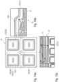
- FIGS. 1-5 b show an example of a pressure sensor 10 .
- the pressure sensor 10 may be used for transducing a pressure measurement into an electric signal.
- the pressure measurement may be, for example, a measurement of a pressure or a measurement indicating a modification of the pressure with time.
- the pressure sensor 10 may be (or may be a part of) a microphone, which may therefore transduce acoustic waves (e.g., sound ultrasound, etc.) into electric signals.
- the pressure sensor 10 may be a microelectromechanical system (MEMS).
- MEMS microelectromechanical system
- the pressure sensor 10 may provide pressure measurement information to external devices and/or compute the pressure measurement information.
- the pressure sensor 10 may have planar dimensions within 1.5 mm and 2 mm (e.g., around 1.7 mm) and a thickness between 0.6 mm and 10 mm (e.g., around 0.8 mm). (The thickness in FIG. 4 is represented as the vertical dimension).
- the pressure sensor 10 may include a lidless structure 30 .
- the lidless structure 30 may be a laminate structure.
- the lidless structure 30 may be in synthetic material (e.g., fiber reinforced (riched) resin).
- the lidless structure 30 may be box-shaped.
- the lidless structure 30 may have a parallelepiped shape or a cylindrical shape.
- the lidless structure 30 may be hollow.
- the lidless structure 30 may, for example, present a plurality of walls 31 , 32 , 33 and 34 (e.g., parallel in a two-by-two fashion).
- the structure 30 may present a floor wall 34 or circuitry-side wall 34 .
- the floor wall 34 or circuitry-side floor wall 34 may be placed at a circuitry-side 30 b of the structure 30 (e.g., back side 30 b ).
- the structure 30 may present an aperture wall 31 or ceiling wall 31 , which may be placed at membrane-side 30 a of the structure 30 .
- the walls 31 and 34 may be spaced from each other through a void space (e.g., chamber or backspace 62 ).
- the floor wall 34 may be parallel to the ceiling wall 31 .
- the structure 30 may include at least one lateral wall (e.g., 32 , 33 ), which may also define an interspace (e.g., chamber 62 ). At least two lateral walls may be parallel to each other.
- the structure 30 may define an internal chamber 62 (back space, cavity) (e.g., delimited within the walls 31 - 34 ).
- the structure 30 may present an aperture 63 .
- the aperture 63 e.g., positioned at the aperture side 30 a
- the wall 31 may be present in the wall 31 .
- the pressure sensor 10 may include a chip 20 .
- the chip 20 may be a MEMS chip.
- the chip 20 may be or include a MEMS device 21 .
- the MEMS device 21 may provide pressure measurements operating as a variable-gap capacitor, which modifies the capacitance based on the pressure.
- the MEMS device 21 may be integrated in the laminate structure 30 , to form a lidless package microphone.
- FIGS. 19 a -19 c Examples of the MEMS device 21 are shown in FIGS. 19 a -19 c .
- FIG. 19 a shows the MEMS device 21 (e.g., the MEMS device 21 of FIG. 1 ).
- FIGS. 19 b and 19 c show two different cross-sectional views according to the line A-A of FIG. 19 a .
- the MEMS device 21 may comprise a membrane 24 and at least one back plate 25 .
- the MEMS device 21 may have one back plate 25 ( FIG. 19 b ).
- the back plate 25 may be more internal than the membrane 24 (e.g., the back plate 25 may be closer to the aperture 63 than the membrane 24 ).
- the back plate 25 may be more external than the membrane 24 (e.g., the back plate 25 may be less close to the aperture 63 than the membrane 24 ).
- the MEMS device 21 may have two back plates 25 ( FIG. 19 c ).
- the membrane 24 may be interposed between two back plates 25 .
- a first back plate 25 may be more internal than the membrane 24 (e.g., the first back plate 25 may be closer to the aperture 63 than the membrane 24 ), while a second back plate 25 may be more external than the membrane 24 (e.g., the second back plate 25 may be less close to the aperture 63 than the membrane 24 ).
- the membrane 24 and at least one back plate(s) 25 may be separated from each other by a gap 26 interposed therebetween.
- the back plate(s) 25 may be in conductor material.
- the back plate(s) 25 may have through-holes for permitting the fluid communication (from the external environment or from an internal environment) to arrive to a surface of the membrane 24 .
- the membrane 24 may be a pressure-sensitive membrane.
- the membrane 24 may be in a synthetic material, e.g., Si nitrite.
- the membrane 24 may deform due to the pressure (e.g., acoustic pressure, such as sound, ultrasound, etc.). Different pressures may lead to different deformations (e.g., greater deformation for greater external pressure).
- the membrane 24 may be fixed to the structure 30 , in particular in correspondence with the rim of the membrane 24 .
- the membrane 24 may vibrate, e.g., in a fashion which is associated to acoustic waves.
- the membrane 24 may be in a conductor material.
- the membrane 24 may form a capacitor(s) together with the at least one back plate 25 (in case of two back plates, two capacitors are actually obtained).
- numeral 21 may be understood as referring to the MEMS device 21 including, for example, both the membrane 24 , the back plate 25 , and the gap 26 .
- the back plate(s) 25 may be fixed to the structure 30 .
- the back plate(s) 25 may be a rigid element.
- the membrane 24 may be a resistor (in this case, the back plate may be avoided).
- the resistance of the resistor may change according to the deformation of the membrane, which in turn follows the pressure.
- reference numeral 21 may be understood as referring to a membrane-based MEMS device which permits to determine pressure information on the basis of the modification of at least one electric parameter (capacitance, resistance, impedance, etc.) associated to the deformation of the membrane 24 .
- the examples below may be understood as including at least one examples of the MEMS device 21 (including at least the membrane 24 ) as above, even the different elements (such as the membrane and the back plate(s)) are not shown in detail.
- the chip 20 (including the MEMS device 21 ) may be mounted on the structure 30 so as to be outside of the structure 30 .
- the chip 20 may be mounted from an external side of the structure 30 .
- the chip 20 can be mounted in correspondence to an external side 31 a of the wall 31 .
- the chip 20 may be outside the internal chamber 62 of the structure 30 .
- the operation of mounting the chip 20 onto the structure 30 can be performed more easily, while the dimension of the structure 30 (in particular the thickness of the structure 30 ) may be advantageously reduced.
- the aperture wall 31 is integral in one piece with the lidless structure 30 (e.g., integral in one piece with the walls 32 and/or 33 ) there is no need, when mounting the chip 20 onto the structure 30 , for applying a lid to the structure 30 . Accordingly, there is no need for glue or bond between the aperture wall 31 and the walls 32 and 33 of the structure 30 .
- the membrane 24 may cooperate with the structure 30 to define an internal environment 60 formed by the internal chamber 62 , the space within the aperture 63 , and/or a space 64 between the aperture 63 and the membrane 24 of the MEMS device 21 .
- a circuitry 40 may be present in the pressure sensor 10 e.g., supported by the structure 30 .
- the circuitry 40 is applied to the circuitry-side wall 34 (in this case, the circuitry 40 may be embedded, e.g., enclosed within the circuitry wall 34 ).
- the circuitry 40 may be an application-specific integrated circuit (ASIC).
- the circuitry 40 may be or include or be connected to a microprocessor.
- the circuitry 40 may be a digital device or analog device or may comprise digital portions and analog portions.
- the circuitry 40 may provide (e.g., in output) pressure measurement information based on the electric signal associated to the deformation of the membrane 24 .
- the circuitry 40 may generate a digital or analog electric signal associated to the pressure, which may represent, for example, sound or ultrasound waved experienced by the sensor 10 .
- the chip 20 may be connected to the circuitry 40 through electric connections (e.g., 41 - 43 ).
- the electric connections may include, for example, via connections 43 .
- Via connections 43 may be obtained in the circuitry wall.
- Via connections 43 may be obtained in a side wall 33 , wherein the vias extend through the dimension of the wall 33 along the thickness direction of the pressure sensor 10 (e.g., through 1 e extension of the wall 33 ).
- the electric connections may include planar connections 42 , e.g. extending along planar directions of the walls 31 and 34 of the structure 30 .
- Electrical connections 41 may be present for electrically connecting the chip 20 (e.g., the membrane 24 and/or the back plate 25 ) to the circuitry 40 and/or output ports (e.g., pads) 45 . It has been understood that the connections 41 may be flip-chip connections. Flip-chip connections, also known as controlled collapsed chip connection (C4), may be based on soldering terminals of the chip 20 to terminals 41 a on the structure 30 , through bumps that have been deposited onto the terminals 41 and/or 41 a . Accordingly, the chip 20 may not only be electrically connected to the circuitry 40 , but the chip 20 is also steadily mechanically fixed to the structure 30 . This is particularly advantageous, since the chip 20 is mounted from outside. Accordingly, an increased simplicity manufacturing is obtained.
- C4 controlled collapsed chip connection
- a sealing technique may be used.
- glue 22 (or a film) or another sealing component may be used to occupy the interspace 65 between the chip and the structure 30 .
- the glue 22 may be made of a thermoset material.
- the glue 22 may be made of an epoxy resin with filler filled.
- the interspace 65 may be understood as being replenished by a portion of the glue 22 (or the film) which externally surrounds (in a radially, planar direction) the interspace 64 between the MEMS device 21 and the aperture 63 .
- the sealed interspace 65 may have a radial extension which is greater than the radial extension of the aperture 63 , so as to seal the environment 60 .
- the closed environment 60 formed by the elements 62 , 63 , and 64 ).
- the internal pressure of the sealed environment 60 may be a reference pressure, useful for obtaining reliable pressure measurement information following the deformation of the membrane 24 .
- the volume occupied by the glue 22 or film or other sealing element may take a space which is greater than the sealing interspace 65 occupied by the glue 22 .
- this is not a problem, as the space occupied by the glue 22 , which is external to the structure 30 , does not increase the extension of the pressure sensor 10 too much (and, in particular, not excessively in the thickness direction).
- the glue 22 may occupy the external, circumferential space around the chip 20 without causing troubles or without increasing the thickness direction of the pressure sensor 10 .
- the glue 22 or the covering film or another sealing material can also contribute in electrically isolating electric connections (e.g., connections 41 and/or 41 a , and/or 42 ) which otherwise would be exposed. Hence, beside the sealing effect, also an appropriate electrical insulation is achieved.
- FIG. 9 a shows an example of the pressure sensor 10 , in which only some parts are depicted.
- the arrows 63 ′ in correspondence to the aperture 63 refer to the fluid communication between the spaces 64 , 63 , and 62 .
- FIG. 9 b shows a variant of a pressure sensor (e.g., microphone and/or acoustic transducer) 10 ′ in which the aperture is a multiple aperture (e.g., plurality of through-holes 63 a , extending like vias along the thickness direction, hence permitting a fluid communication, indicated by arrows 63 ′, between the space 64 and the chamber 62 ).
- a pressure sensor e.g., microphone and/or acoustic transducer
- FIGS. 10-12 show a variant of a pressure sensor (e.g., microphone and/or acoustic transducer) 10 ′′ in which a film 1022 is placed on the structure 30 (e.g., on the ceiling wall 31 ).
- the film 1022 may be in epoxy or, more in general, in synthetic material.
- the film 1022 may be made of resin base or thermoset material.
- the film 1022 may include at least one of:
- a mounting portion 102265 connecting (e.g., continuously) the ceiling-wall portion 102231 with the MEMS device portion 102221 .
- the film 1022 may seal the closed environment 60 and operate like the seal 22 .
- Flip opening ports 1050 may be operated to the film 1022 (e.g., to the MEMS device portion 102221 ), e.g., by laser cutting. Accordingly, pressure change from ambient can be transferred to the MEMS device 21 .
- FIG. 13 shows a variant of a pressure sensor (e.g., microphone and/or acoustic transducer) 10 ′′′ showing the chip (e.g., MEMS chip) 20 and the circuitry 40 , which has aspects which may be implemented independently from each other.
- a first aspect is that connections 41 may be implemented directly between the chip 20 and the circuitry 40 , e.g., through a flip-chip connection.
- a second aspect (that may be combined with the first aspect) is that the circuitry 40 may be within the chamber 62 , not enclosed in the floor wall 34 .
- the circuitry 40 may be fixed to the floor wall 34 , e.g., through flip-chip connection or through via connections, e.g., to arrive at output ports (e.g., pads) 45 .
- the wall(s) 32 ′ and 33 ′ may be massive, in the sense that the chamber 62 is obtained in a portion which has a planar (e.g., lateral, radial) dimension which is less than 60% of the planar (e.g., lateral, radial) dimension of the structure 30 .
- the structure 30 has here a massive shape, which increase robustness.
- FIG. 14 shows a variant of a pressure sensor (e.g., microphone and/or acoustic transducer) 10 ′′′′ in which the chamber 62 has a planar (e.g., lateral, radial) dimension which is larger than the planar (e.g., lateral, radial) dimension of the aperture 63 (contrary to FIG. 13 , where the chamber 62 has a planar dimension which is the same of the planar dimension of the aperture 63 ).
- a pressure sensor e.g., microphone and/or acoustic transducer
- FIG. 15 shows a variant of a pressure sensor (e.g., microphone and/or acoustic transducer) 10 ′′′′ in which an electrical connection between the chip (e.g., MEMS chip) 20 and the circuitry 40 and/or at least one output port (pad) 45 is obtained through a wire 49 .
- the wired connections are in general less reliable than flip-chip connections, this is not a concern, as the wire 49 may be simply embedded in (e.g., enclosed in, e.g. completely covered by) the sealing material 22 . Therefore, while the stability and the insulation of the electrical connection are guaranteed, the chip 20 may be glued to the structure 30 only by relying on the glue 22 (hence simplifying the manufacturing process). In any case, it is possible to increase the number of electric connections without performing too many flip-chip connections.
- FIGS. 16 a and 16 b show a variant of a pressure sensor (e.g., microphone and/or acoustic transducer) 10 ′′′′′′ in which a protective mesh cover 1626 of a reticular shape is applied over the MEMS device 21 .
- the protective cover 1626 may be in metal material.
- the protective cover 1626 may be in non-metal material.
- the protective cover 1626 may be separated from the MEMS device 21 by a gap 21 ′.
- the protective mesh cover 1626 may protect the membrane 24 from big particle drops.
- FIGS. 17 a -17 c show another example of pressure sensor (e.g., microphone and/or acoustic transducer) 10 ′′′′′.
- the structure 30 in the thickness direction, may have an extension which is similar to that of the chip (e.g., MEMS chip) 20 .
- a manufacturing method 1800 (shown in FIG. 18 ) is explained with particular reference to FIGS. 6 a - 8 b.
- the method 1800 may be a method for preparing or manufacturing a pressure sensor (e.g. the pressure sensor 10 discussed above, and/or another pressure sensor above and/or below).
- the method 1800 may include at least one step 1810 of preparing a laminate structure 30 or 630 (which may be the lidless structure 30 discussed above or a precursor of the lidless structure 30 ).
- the laminate structure 630 may include a plurality of structures 30 for manufacturing a plurality of pressure sensors 10 .
- the structure 30 or 630 may appear as in FIGS. 6 a and 6 b.
- the step 1810 of preparing a laminate structure 30 or 630 may be performed in such a way that the laminate structure 30 or 630 has at least one cavity 62 (e.g., the backspace or chamber 62 above) fluidically communicating with the external environment through an aperture 63 . Accordingly, in this step 1810 , the laminate structure 30 or 630 is open, and the at least one cavity 62 may be in fluid communication with an external environment.
- a circuitry 40 may be applied to the laminate structure 630 or 30 , e.g., during lamination (the circuitry 40 may be embedded, e.g., enclosed, in the material of the walls of the structure 630 or 30 ).
- the laminate structure 630 or 30 may be prepared, e.g., by laminating walls (e.g., ceiling walls 31 and 34 ) so as that they present the precursors 632 and 633 of walls 32 and 33 .
- the precursors 632 and 633 may extend in the planar direction may be integrated in one piece with each other.
- the precursors 632 and 633 may be adjacent with each other and/or integrated and/or substantially indistinguishable from an external sight. Accordingly, several single structures 30 of the structure 630 appear to have the precursors 632 and 633 adjacent to precursors 633 and 632 , respectively, of adjacent structures 30 .
- the circuitries 40 may be applied to the structures 630 .
- the circuitries 40 may be embedded (e.g., enclosed) in the walls 34 (e.g., during lamination).
- the cavities 62 and/or the apertures 63 may be obtained, for example, by drilling (e.g., laser or mechanical drill).
- electric connections may also be prepared.
- the vias 43 performed on the walls 34 and/or on the one precursor 633 .
- Vias 43 may be obtained, for example, by inserting conductive material after having etched walls (or precursors of walls) of the structure 630 or 30 .
- the planar connections 41 a , 42 as well as input/output pads (ports) 45 may be made.
- a step may be performed, when preparing the laminate structure, of also preparing the through-holes 63 a .
- the chip 20 may include a MEMS device 21 .
- the MEMS device 21 may include the membrane 24 , deformable on the basis of external pressure, which may be placed in correspondence to the aperture 63 .
- the MEMS device 21 may also comprise a backplate 25 (e.g., for forming a capacitance with the membrane 24 ). Accordingly, the membrane 24 may be an element which closes the internal environment 62 .
- the chip 20 may be connected, for example, through flip-chip connections, e.g., by bumping terminals of the chip 20 and/or terminals 41 a on the structure 30 , so as to electrically and/or mechanically connect the flip-chip to the other parts of the pressure sensor 10 to be manufactured.
- flip-chip connections e.g., by bumping terminals of the chip 20 and/or terminals 41 a on the structure 30 , so as to electrically and/or mechanically connect the flip-chip to the other parts of the pressure sensor 10 to be manufactured.
- the sealing material which may be glue 22
- sealing material 22 or 1022 may be, for example, glue 22 or a film.
- the sealing material is the film 1022 (see FIGS. 10-12 )
- the laser cutting e.g., laser drilling
- the flip opening ports 1050 may be performed for obtaining the flip opening ports 1050 .
- the structure 630 may therefore be singulated.
- the laminate structure 630 may be sawed, e.g., in correspondence to the adjacent wall precursor 632 , 633 .
- the walls 32 and 33 of the structure 30 are obtained. Further, the different pressure sensors 10 are obtained.
- the step 1830 of applying the sealing material may include the step of applying a film 1022 on the structure 1033 (see above), and, in case, laser cutting to obtain the flip openings 1050 .
- the circuitry 40 may be configured to provide the pressure measurement information by transducing waves of acoustic pressure(s) (e.g., sound, ultrasound, etc.) into an electric signal.
- the electric signal may be output (e.g., though pads 45 ) and transmitted (e.g., via an antenna or a wired connection) and/or stored in a storage unit.
- the electric signal may therefore be used (e.g., by a loudspeaker) for reproducing sound at a remote position and/or at a subsequent time instant.
- MEMS components may be embodied by MEMS components to obtain MEMS pressure sensors, such as MEMS microphones and MEMS acoustic transducers.
- the chips 20 may be MEMS chips, and/or the membrane 24 may be a MEMS membrane (and may be part of the MEMS device 21 ).
- the glue 22 (or the film 1022 ) may be applied to an external side 31 a of the ceiling wall 31 which presents a clearly much larger extension than the extension of the than the walls 32 and 33 n the thickness planar, radial direction.
- glue should be placed on the lid only in correspondence of the small extension of the walls 32 and 33 , which would be difficult and would result into a breakable structure.
- the extension in the planar, radial direction is reduced, e.g., when the circuitry 40 is applied to the floor wall 34 or to a wall which is different from the ceiling wall 31 .
- lateral wall(s) e.g., 33
- vias which may permit to have internal conductors 43 , hence maximizing the use of the space.
- flip-chip connections may permit to have good mechanical and electrical connections.
- the wire 49 When a wire 49 is used (see FIGS. 15 and 16 a ), the wire 49 may be easily covered by the glue, which, when solidified, provides good insulation and mechanical protection.
- the application of the film 1022 may be easily performed and the film 1022 may be easily cut with laser cutting (drilling).
Landscapes
- Physics & Mathematics (AREA)
- Engineering & Computer Science (AREA)
- General Physics & Mathematics (AREA)
- Signal Processing (AREA)
- Acoustics & Sound (AREA)
- Microelectronics & Electronic Packaging (AREA)
- Manufacturing & Machinery (AREA)
- Chemical & Material Sciences (AREA)
- Analytical Chemistry (AREA)
- Computer Hardware Design (AREA)
- Micromachines (AREA)
- Electrostatic, Electromagnetic, Magneto- Strictive, And Variable-Resistance Transducers (AREA)
- Pressure Sensors (AREA)
Abstract
Description
Claims (16)
Applications Claiming Priority (2)
| Application Number | Priority Date | Filing Date | Title |
|---|---|---|---|
| EP19187635.8A EP3770112A1 (en) | 2019-07-22 | 2019-07-22 | Pressure sensor |
| EP19187635 | 2019-07-22 |
Publications (2)
| Publication Number | Publication Date |
|---|---|
| US20210025774A1 US20210025774A1 (en) | 2021-01-28 |
| US11274984B2 true US11274984B2 (en) | 2022-03-15 |
Family
ID=67438412
Family Applications (1)
| Application Number | Title | Priority Date | Filing Date |
|---|---|---|---|
| US16/890,461 Active 2040-07-09 US11274984B2 (en) | 2019-07-22 | 2020-06-02 | Pressure sensor having a lidless/laminate structure |
Country Status (3)
| Country | Link |
|---|---|
| US (1) | US11274984B2 (en) |
| EP (1) | EP3770112A1 (en) |
| CN (1) | CN112291690B (en) |
Citations (7)
| Publication number | Priority date | Publication date | Assignee | Title |
|---|---|---|---|---|
| US7447323B2 (en) | 1999-09-07 | 2008-11-04 | Pulse Mems Aps | Surface mountable transducer system |
| US20100164028A1 (en) * | 2007-09-25 | 2010-07-01 | Takuya Adachi | Semiconductor pressure sensor |
| US20100195864A1 (en) | 2007-08-02 | 2010-08-05 | Nxp B.V. | Electro-acoustic transducer comprising a mems sensor |
| US20150285703A1 (en) * | 2012-10-17 | 2015-10-08 | Kabushiki Kaisha Saginomiya Seisakusho | Pressure sensor, and sensor unit provided with same |
| US20160091378A1 (en) * | 2014-09-29 | 2016-03-31 | Invensense, Inc. | Microelectromechanical systems (mems) pressure sensor having a leakage path to a cavity |
| US20160153857A1 (en) * | 2014-11-28 | 2016-06-02 | Seiko Epson Corporation | Electronic device, physical quantity sensor, pressure sensor, vibrator, altimeter, electronic apparatus, and moving object |
| US20180275001A1 (en) * | 2017-03-22 | 2018-09-27 | Azbil Corporation | Pressure sensor chip, pressure transmitter, and method for manufacturing pressure sensor chip |
Family Cites Families (7)
| Publication number | Priority date | Publication date | Assignee | Title |
|---|---|---|---|---|
| FR2628282B1 (en) * | 1988-03-01 | 1990-08-24 | Horlogerie Photograph Fse | ELECTROACOUSTIC CAPSULE WITH PIEZOELECTRIC MEMBRANE |
| EP0595514B1 (en) * | 1992-10-27 | 2003-06-25 | TDK Corporation | Piezoelectric transducer |
| AU6984000A (en) * | 1999-09-06 | 2001-04-10 | ROMBACH, Pirmin, Hernann, Otto | A pressure transducer |
| TWI444052B (en) * | 2009-12-17 | 2014-07-01 | Ind Tech Res Inst | Capacitive transducer and fabrication method |
| US8375560B2 (en) * | 2011-02-22 | 2013-02-19 | Taiwan Carol Electronics Co., Ltd. | Method for manufacturing a condenser microphone |
| ITUB20160759A1 (en) * | 2016-02-15 | 2017-08-15 | St Microelectronics Srl | ENCAPSULATED PRESSURE SENSOR IN ELASTOMERIC MATERIAL, AND SYSTEM INCLUDING THE PRESSURE SENSOR |
| JP6809008B2 (en) * | 2016-07-08 | 2021-01-06 | オムロン株式会社 | MEMS structure and capacitance type sensor, piezoelectric type sensor, acoustic sensor having MEMS structure |
-
2019
- 2019-07-22 EP EP19187635.8A patent/EP3770112A1/en active Pending
-
2020
- 2020-06-02 US US16/890,461 patent/US11274984B2/en active Active
- 2020-07-21 CN CN202010704242.4A patent/CN112291690B/en active Active
Patent Citations (7)
| Publication number | Priority date | Publication date | Assignee | Title |
|---|---|---|---|---|
| US7447323B2 (en) | 1999-09-07 | 2008-11-04 | Pulse Mems Aps | Surface mountable transducer system |
| US20100195864A1 (en) | 2007-08-02 | 2010-08-05 | Nxp B.V. | Electro-acoustic transducer comprising a mems sensor |
| US20100164028A1 (en) * | 2007-09-25 | 2010-07-01 | Takuya Adachi | Semiconductor pressure sensor |
| US20150285703A1 (en) * | 2012-10-17 | 2015-10-08 | Kabushiki Kaisha Saginomiya Seisakusho | Pressure sensor, and sensor unit provided with same |
| US20160091378A1 (en) * | 2014-09-29 | 2016-03-31 | Invensense, Inc. | Microelectromechanical systems (mems) pressure sensor having a leakage path to a cavity |
| US20160153857A1 (en) * | 2014-11-28 | 2016-06-02 | Seiko Epson Corporation | Electronic device, physical quantity sensor, pressure sensor, vibrator, altimeter, electronic apparatus, and moving object |
| US20180275001A1 (en) * | 2017-03-22 | 2018-09-27 | Azbil Corporation | Pressure sensor chip, pressure transmitter, and method for manufacturing pressure sensor chip |
Also Published As
| Publication number | Publication date |
|---|---|
| EP3770112A1 (en) | 2021-01-27 |
| CN112291690B (en) | 2024-04-05 |
| US20210025774A1 (en) | 2021-01-28 |
| CN112291690A (en) | 2021-01-29 |
Similar Documents
| Publication | Publication Date | Title |
|---|---|---|
| US8837754B2 (en) | Microelectromechanical transducer and corresponding assembly process | |
| US9337354B2 (en) | Top port MEMS cavity package and method of manufacture thereof | |
| US10329143B2 (en) | Package with chambers for dies and manufacturing process thereof | |
| US8184845B2 (en) | Electrical module comprising a MEMS microphone | |
| US9108840B2 (en) | MEMS microphone and method for packaging the same | |
| CN101815235B (en) | Miniature MEMS condenser microphone packages and fabrication method thereof | |
| CN102131139B (en) | Microphone package of micro-electro-mechanical system and manufacturing method thereof | |
| CN104105017B (en) | Microphone | |
| US20160345106A1 (en) | Multi-mems module | |
| US8999757B2 (en) | Top port MEMS cavity package and method of manufacture thereof | |
| US8354747B1 (en) | Conductive polymer lid for a sensor package and method therefor | |
| CN104080033B (en) | Microphone | |
| CN212393006U (en) | Bone voiceprint sensor and electronic device | |
| CN109644307B (en) | Microphone and pressure sensor package and method of making microphone and pressure sensor package | |
| US10405102B2 (en) | MEMS transducer package | |
| US11274984B2 (en) | Pressure sensor having a lidless/laminate structure | |
| CN109644309A (en) | Transducer package with via hole | |
| CN119172711A (en) | Combined acoustic transducer and pressure sensor package | |
| WO2022239442A1 (en) | Differential pressure sensor and method for manufacturing same | |
| CN115340061A (en) | MEMS chip packaging structure, ultrasonic sensor with MEMS chip packaging structure and packaging process |
Legal Events
| Date | Code | Title | Description |
|---|---|---|---|
| AS | Assignment |
Owner name: INFINEON TECHNOLOGIES AG, GERMANY Free format text: ASSIGNMENT OF ASSIGNORS INTEREST;ASSIGNORS:CHIANG, CHAU FATT;CALO, PAUL ARMAND ASENTISTA;CHA, CHAN LAM;AND OTHERS;SIGNING DATES FROM 20200521 TO 20200601;REEL/FRAME:052812/0884 |
|
| FEPP | Fee payment procedure |
Free format text: ENTITY STATUS SET TO UNDISCOUNTED (ORIGINAL EVENT CODE: BIG.); ENTITY STATUS OF PATENT OWNER: LARGE ENTITY |
|
| STPP | Information on status: patent application and granting procedure in general |
Free format text: APPLICATION DISPATCHED FROM PREEXAM, NOT YET DOCKETED |
|
| STPP | Information on status: patent application and granting procedure in general |
Free format text: DOCKETED NEW CASE - READY FOR EXAMINATION |
|
| STPP | Information on status: patent application and granting procedure in general |
Free format text: NON FINAL ACTION MAILED |
|
| STPP | Information on status: patent application and granting procedure in general |
Free format text: RESPONSE TO NON-FINAL OFFICE ACTION ENTERED AND FORWARDED TO EXAMINER |
|
| STPP | Information on status: patent application and granting procedure in general |
Free format text: NOTICE OF ALLOWANCE MAILED -- APPLICATION RECEIVED IN OFFICE OF PUBLICATIONS |
|
| STPP | Information on status: patent application and granting procedure in general |
Free format text: AWAITING TC RESP., ISSUE FEE NOT PAID |
|
| STPP | Information on status: patent application and granting procedure in general |
Free format text: NOTICE OF ALLOWANCE MAILED -- APPLICATION RECEIVED IN OFFICE OF PUBLICATIONS |
|
| STCF | Information on status: patent grant |
Free format text: PATENTED CASE |
|
| MAFP | Maintenance fee payment |
Free format text: PAYMENT OF MAINTENANCE FEE, 4TH YEAR, LARGE ENTITY (ORIGINAL EVENT CODE: M1551); ENTITY STATUS OF PATENT OWNER: LARGE ENTITY Year of fee payment: 4 |