US11269771B2 - Storage device for improving journal replay, operating method thereof, and electronic device including the storage device - Google Patents
Storage device for improving journal replay, operating method thereof, and electronic device including the storage device Download PDFInfo
- Publication number
- US11269771B2 US11269771B2 US16/818,418 US202016818418A US11269771B2 US 11269771 B2 US11269771 B2 US 11269771B2 US 202016818418 A US202016818418 A US 202016818418A US 11269771 B2 US11269771 B2 US 11269771B2
- Authority
- US
- United States
- Prior art keywords
- journal
- area
- segments
- meta data
- controller
- Prior art date
- Legal status (The legal status is an assumption and is not a legal conclusion. Google has not performed a legal analysis and makes no representation as to the accuracy of the status listed.)
- Active, expires
Links
Images


Classifications
-
- G—PHYSICS
- G06—COMPUTING; CALCULATING OR COUNTING
- G06F—ELECTRIC DIGITAL DATA PROCESSING
- G06F12/00—Accessing, addressing or allocating within memory systems or architectures
- G06F12/02—Addressing or allocation; Relocation
- G06F12/0223—User address space allocation, e.g. contiguous or non contiguous base addressing
- G06F12/023—Free address space management
- G06F12/0238—Memory management in non-volatile memory, e.g. resistive RAM or ferroelectric memory
- G06F12/0246—Memory management in non-volatile memory, e.g. resistive RAM or ferroelectric memory in block erasable memory, e.g. flash memory
-
- G—PHYSICS
- G06—COMPUTING; CALCULATING OR COUNTING
- G06F—ELECTRIC DIGITAL DATA PROCESSING
- G06F12/00—Accessing, addressing or allocating within memory systems or architectures
- G06F12/02—Addressing or allocation; Relocation
- G06F12/0223—User address space allocation, e.g. contiguous or non contiguous base addressing
- G06F12/0292—User address space allocation, e.g. contiguous or non contiguous base addressing using tables or multilevel address translation means
-
- G—PHYSICS
- G06—COMPUTING; CALCULATING OR COUNTING
- G06F—ELECTRIC DIGITAL DATA PROCESSING
- G06F12/00—Accessing, addressing or allocating within memory systems or architectures
- G06F12/02—Addressing or allocation; Relocation
- G06F12/08—Addressing or allocation; Relocation in hierarchically structured memory systems, e.g. virtual memory systems
- G06F12/0802—Addressing of a memory level in which the access to the desired data or data block requires associative addressing means, e.g. caches
- G06F12/0804—Addressing of a memory level in which the access to the desired data or data block requires associative addressing means, e.g. caches with main memory updating
-
- G—PHYSICS
- G06—COMPUTING; CALCULATING OR COUNTING
- G06F—ELECTRIC DIGITAL DATA PROCESSING
- G06F12/00—Accessing, addressing or allocating within memory systems or architectures
- G06F12/02—Addressing or allocation; Relocation
- G06F12/08—Addressing or allocation; Relocation in hierarchically structured memory systems, e.g. virtual memory systems
- G06F12/0802—Addressing of a memory level in which the access to the desired data or data block requires associative addressing means, e.g. caches
- G06F12/0877—Cache access modes
- G06F12/0882—Page mode
-
- G—PHYSICS
- G06—COMPUTING; CALCULATING OR COUNTING
- G06F—ELECTRIC DIGITAL DATA PROCESSING
- G06F12/00—Accessing, addressing or allocating within memory systems or architectures
- G06F12/02—Addressing or allocation; Relocation
- G06F12/08—Addressing or allocation; Relocation in hierarchically structured memory systems, e.g. virtual memory systems
- G06F12/10—Address translation
- G06F12/1009—Address translation using page tables, e.g. page table structures
-
- G—PHYSICS
- G06—COMPUTING; CALCULATING OR COUNTING
- G06F—ELECTRIC DIGITAL DATA PROCESSING
- G06F16/00—Information retrieval; Database structures therefor; File system structures therefor
- G06F16/10—File systems; File servers
- G06F16/18—File system types
- G06F16/1805—Append-only file systems, e.g. using logs or journals to store data
- G06F16/1815—Journaling file systems
-
- G—PHYSICS
- G06—COMPUTING; CALCULATING OR COUNTING
- G06F—ELECTRIC DIGITAL DATA PROCESSING
- G06F3/00—Input arrangements for transferring data to be processed into a form capable of being handled by the computer; Output arrangements for transferring data from processing unit to output unit, e.g. interface arrangements
- G06F3/06—Digital input from, or digital output to, record carriers, e.g. RAID, emulated record carriers or networked record carriers
- G06F3/0601—Interfaces specially adapted for storage systems
- G06F3/0628—Interfaces specially adapted for storage systems making use of a particular technique
- G06F3/0655—Vertical data movement, i.e. input-output transfer; data movement between one or more hosts and one or more storage devices
- G06F3/0656—Data buffering arrangements
-
- G—PHYSICS
- G06—COMPUTING; CALCULATING OR COUNTING
- G06F—ELECTRIC DIGITAL DATA PROCESSING
- G06F3/00—Input arrangements for transferring data to be processed into a form capable of being handled by the computer; Output arrangements for transferring data from processing unit to output unit, e.g. interface arrangements
- G06F3/06—Digital input from, or digital output to, record carriers, e.g. RAID, emulated record carriers or networked record carriers
- G06F3/0601—Interfaces specially adapted for storage systems
- G06F3/0628—Interfaces specially adapted for storage systems making use of a particular technique
- G06F3/0655—Vertical data movement, i.e. input-output transfer; data movement between one or more hosts and one or more storage devices
- G06F3/0658—Controller construction arrangements
-
- G—PHYSICS
- G06—COMPUTING; CALCULATING OR COUNTING
- G06F—ELECTRIC DIGITAL DATA PROCESSING
- G06F3/00—Input arrangements for transferring data to be processed into a form capable of being handled by the computer; Output arrangements for transferring data from processing unit to output unit, e.g. interface arrangements
- G06F3/06—Digital input from, or digital output to, record carriers, e.g. RAID, emulated record carriers or networked record carriers
- G06F3/0601—Interfaces specially adapted for storage systems
- G06F3/0668—Interfaces specially adapted for storage systems adopting a particular infrastructure
- G06F3/0671—In-line storage system
- G06F3/0673—Single storage device
- G06F3/0679—Non-volatile semiconductor memory device, e.g. flash memory, one time programmable memory [OTP]
-
- G—PHYSICS
- G06—COMPUTING; CALCULATING OR COUNTING
- G06F—ELECTRIC DIGITAL DATA PROCESSING
- G06F2212/00—Indexing scheme relating to accessing, addressing or allocation within memory systems or architectures
- G06F2212/10—Providing a specific technical effect
- G06F2212/1032—Reliability improvement, data loss prevention, degraded operation etc
-
- G—PHYSICS
- G06—COMPUTING; CALCULATING OR COUNTING
- G06F—ELECTRIC DIGITAL DATA PROCESSING
- G06F2212/00—Indexing scheme relating to accessing, addressing or allocation within memory systems or architectures
- G06F2212/60—Details of cache memory
- G06F2212/608—Details relating to cache mapping
-
- G—PHYSICS
- G06—COMPUTING; CALCULATING OR COUNTING
- G06F—ELECTRIC DIGITAL DATA PROCESSING
- G06F2212/00—Indexing scheme relating to accessing, addressing or allocation within memory systems or architectures
- G06F2212/72—Details relating to flash memory management
- G06F2212/7201—Logical to physical mapping or translation of blocks or pages
Definitions
- Exemplary embodiments of the inventive concept described herein relate to a storage device for improving a journal replay, an operating method thereof, and an electronic device including the storage device
- a storage device that is a nonvolatile storage medium may retain data permanently or semipermanently regardless of whether a power is supplied thereto.
- the storage device may include both a nonvolatile memory and a volatile memory that is smaller in capacity than the nonvolatile memory but has a fast input/output speed.
- the storage device may use the volatile memory as a cache memory with regard to the nonvolatile memory.
- the storage device may store data stored in the volatile memory in the nonvolatile memory.
- a storage device includes a nonvolatile memory including a main meta data area and a journal area, and a controller.
- the controller updates an address mapping table including a plurality of page mapping entries divided into a plurality of segments by executing a flash translation layer (FTL) stored in a working memory, stores updated page mapping entries of the plurality of page mapping entries in the journal area as journal data, and stores the plurality of segments, each having a size smaller than a physical page of the nonvolatile memory, in the main meta data area.
- FTL flash translation layer
- the operating method includes updating, by the controller, an address mapping table including a plurality of page mapping entries, storing updated page mapping entries of the plurality of page mapping entries in the journal area as journal data, and storing a plurality of segments in the main meta data area based on an order in which the updated page mapping entries are stored in the journal area and the number of the updated page mapping entries of each of the plurality of segments dividing the plurality of page mapping entries.
- FTL flash translation layer
- an electronic device includes a host configured to transmit a request including a logical address, and a storage device including a nonvolatile memory and a controller.
- the nonvolatile memory includes a main meta data area and a journal area.
- the controller is further configured to update an address mapping table including a plurality of page mapping entries divided into a plurality of segments by processing the request of the host, store updated page mapping entries of the plurality of page mapping entries in the journal area as journal data, and store the plurality of segments, each having a size smaller than a physical page of the nonvolatile memory, in the main meta data area.
- FIG. 1 illustrates a block diagram of an electronic device according to an exemplary embodiment of the inventive concept.
- FIG. 2 illustrates a block diagram of an electronic device according to an exemplary embodiment of the inventive concept.
- FIGS. 3 to 6 illustrate diagrams for describing how a controller according to an exemplary embodiment of the inventive concept stores meta data in a nonvolatile memory.
- FIGS. 7 and 8 illustrate examples where a controller stores meta data together with timestamps according to exemplary embodiments of the inventive concept.
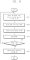
- FIG. 9 illustrates a flowchart including processes where a controller according to an exemplary embodiment of the inventive concept stores an address mapping table in a nonvolatile memory.
- FIG. 10 illustrates a flowchart including detailed operations constituting operation S 160 of FIG. 9 according to an exemplary embodiment of the inventive concept.
- FIG. 11 illustrates a flowchart including a process where a controller according to an exemplary embodiment of the inventive concept recovers an address mapping table.
- FIG. 12 illustrates a block diagram of a controller of FIG. 1 in detail according to an exemplary embodiment of the inventive concept.
- FIG. 13 illustrates a block diagram of a controller of FIG. 2 in detail according to an exemplary embodiment of the inventive concept.
- FIG. 14 illustrates a block diagram of an electronic device according to an exemplary embodiment of the inventive concept.
- FIG. 15 is a block diagram illustrating a computing system including a storage device according to an exemplary embodiment of the inventive concept.
- Exemplary embodiments of the inventive concept provide a storage device for improving a journal replay, an operating method thereof, and an electronic device including the storage device.
- FIG. 1 illustrates a block diagram of an electronic device according to an exemplary embodiment of the inventive concept.
- An electronic device 10 a may be a personal computer, a workstation, a notebook, a tablet, a mobile device, or a smartphone, and may be referred to as a “computing system”, an “electronic system”, or a “mobile system”.
- the electronic device 10 a may include a host 11 and a storage device 100 a.
- the host 11 may transmit a command CMD to the storage device 100 a .
- the host 11 may exchange data “DATA” with the storage device 100 a .
- the host 11 may receive a response RSP to the command CMD from the storage device 100 a .
- the host 11 may be implemented to include one or more processor cores.
- the host 11 may include a general-purpose processor, a special-purpose processor, or an application processor.
- the host 11 may be a processor itself, or the host 11 may be an electronic device or a system including a processor.
- the storage device 100 a may communicate with the host 11 in compliance with various interface protocols.
- the storage device 100 a may be a solid state drive (SSD), an embedded memory card integrated in the electronic device 10 a , a memory card removable from the electronic device 10 a , a secure digital (SD) card, an embedded multimedia card (eMMC), a universal flash storage (UFS) card, etc.
- the storage device 100 a may include a controller 110 a and a nonvolatile memory 130 .
- the controller 110 a may write the data “DATA” in the nonvolatile memory 130 based on the command CMD of the host 11 ; alternatively, based on the command CMD of the host 11 , the controller 110 a may read the data “DATA” from the nonvolatile memory 130 and may transmit the read data “DATA” to the host 11 .
- the controller 110 a may process the command CMD, and may transmit the response RSP indicating a processing result to the host 11 .
- the controller 110 a may include a working memory 112 a having a faster data input/output speed than the nonvolatile memory 130 .
- the controller 110 a may use the working memory 112 a as a cache memory.
- the controller 110 a may execute a flash translation layer (FTL) stored in the working memory 112 a .
- the FTL may be loaded onto the working memory 112 a as firmware or a program stored in a ROM or the nonvolatile memory 130 of the storage device 100 a .
- the FTL may be present between a file system (refer to FIG. 14 ) of the host 11 and the nonvolatile memory 130 .
- the FTL may perform an address mapping operation to manage mapping between a logical address provided from the host 11 and a physical address of the nonvolatile memory 130 .
- the FTL may further perform a garbage collection operation, a wear leveling operation, or the like, as well as the address mapping operation.
- the FTL may be executed by the controller 110 a to address the following limitations of the nonvolatile memory 130 : overwrite- or in-place write-impossible, a lifetime of a memory cell, a limited number of program/erase cycles, and an erase speed slower than a write speed.
- the FTL may update an address mapping table AMT including information about mapping between the logical address and the physical address.
- the address mapping table AMT may be stored in the working memory 112 a.
- the FTL may manage a segment mapping table SMT indicating a location of the nonvolatile memory 130 , in which the mapping information of the address mapping table AMT is stored.
- the segment mapping table SMT may be stored in the working memory 112 a , and a size of the segment mapping table SMT may be smaller than a size of the address mapping table AMT.
- the FTL may update a portion (part) of the mapping information of the address mapping table AMT, and may store update information of the address mapping table AMT in a journal buffer JB.
- the journal buffer JB may be located at the working memory 112 a.
- the working memory 112 a may include or store the FTL, the address mapping table AMT, the segment mapping table SMT, and the journal buffer JB.
- the working memory 112 a may include an area for storing the FTL, an area for storing the address mapping table AMT, an area for storing the segment mapping table SMT, and an area that is allocated to the journal buffer JB, and the controller 110 a may in advance set the above areas in the working memory 112 a or may adjust the above areas according to a request of the host 11 or a user.
- the working memory 112 a may be a storage medium or an on-chip memory including a latch, a register, a static random access memory (SRAM), a dynamic random access memory (DRAM), a thyristor random access memory (TRAM), a tightly coupled memory (TCM), etc.
- SRAM static random access memory
- DRAM dynamic random access memory
- TCM tightly coupled memory
- the nonvolatile memory 130 may store (or write or program) data, or may provide data stored therein to the controller 110 a .
- the nonvolatile memory 130 may include a user data area USER DATA and an over-provisioning area OP.
- the user data area USER DATA may be an area allocated to the host 11 and may store data based on a request of the host 11 .
- the over-provisioning area OP may not be an area allocated to the host 11 and may not be open to the host 11 .
- the controller 110 a may use the over-provisioning area OP for managing the nonvolatile memory 130 .
- the over-provisioning area OP may be also referred to as a “meta data area”.
- meta data stored in the working memory 112 a may be lost when power events, such as sudden power off (SPO) or system crash (volatile), occur.
- the meta data may include the address mapping table AMT, the segment mapping table SMT, and update information (hereinafter referred to as “journal data”) of the address mapping table AMT stored in the journal buffer JB.
- the meta data may further include information about a read/write unit (e.g., a page) of the nonvolatile memory 130 , information about an erase unit (e.g., a block BLK (refer to FIG. 14 )) of the nonvolatile memory 130 , etc.
- the controller 110 a may store the meta data stored in the working memory 112 a in the over-provisioning area OP of the nonvolatile memory 130 .
- the FTL may store the address mapping table AMT in main meta data areas MMA 1 and MMA 2 , may store the segment mapping table SMT in a segment mapping table area SMTA, and may store journal data stored in the journal buffer JB in journal areas JA 1 and JA 2 .
- the controller 110 a may set in advance the above areas in the working memory 112 a , or may adjust the above-described areas depending on a request of the host 11 or the user.
- the nonvolatile memory 130 may include nonvolatile memory cells such as a NAND flash memory cell, a NOR flash memory cell, a resistive random access memory (RRAM) cell, a ferroelectric random access memory (FRAM) cell, a phase change random access memory (PRAM) cell, or a magnetic random access memory (MRAM) cell.
- nonvolatile memory cells such as a NAND flash memory cell, a NOR flash memory cell, a resistive random access memory (RRAM) cell, a ferroelectric random access memory (FRAM) cell, a phase change random access memory (PRAM) cell, or a magnetic random access memory (MRAM) cell.
- FIG. 2 illustrates a block diagram of an electronic device according to an exemplary embodiment of the inventive concept.
- An electronic device 10 b may include the host 11 and a storage device 100 b .
- the electronic device 10 b may be substantially identical to the electronic device 10 a except for the storage device 100 b .
- the storage device 100 b may include a controller 110 b and the nonvolatile memory 130 .
- the storage device 100 b may further include a buffer memory 120 .
- the controller 110 b may include a working memory 112 b that is substantially identical to the working memory 112 a , and may further use the buffer memory 120 as a cache memory unlike the controller 110 a .
- the buffer memory 120 may be located outside the controller 110 b.
- the controller 110 b may store and load the address mapping table AMT onto the buffer memory 120 . Unlike the example illustrated in FIG. 1 , the controller 110 b may store and load the address mapping table AMT onto both the working memory 112 b and the buffer memory 120 . As a capacity of the nonvolatile memory 130 increases, a size of the address mapping table AMT may increase. In this case, the address mapping table AMT may be stored in the buffer memory 120 located outside the controller 110 b .
- the buffer memory 120 may be a storage medium including a latch, a register, an SRAM, a DRAM, a TRAM, a TCM, etc.
- the controller 110 b may store and load the FTL, the segment mapping table SMT, and the journal buffer JB onto the working memory 112 b .
- An operation of the storage device 100 b may be similar to the operation of the storage device 100 a , except that the storage device 100 b further includes the buffer memory 120 .
- a storage device 100 may refer to one of the storage devices 100 a and 100 b
- a controller 110 may refer to one of the controllers 110 a and 110 b
- a working memory 112 may refer to one of the working memories 112 a and 112 b.
- the FTL that is executed by the controller 110 of the storage device 100 may reduce a time or cost to perform a journal replay for recovering the address mapping table AMT loaded onto the working memory 112 or the buffer memory 120 based on information read from the journal areas JA 1 and JA 2 of the nonvolatile memory 130 .
- FIGS. 3 to 6 illustrate diagrams for describing how a controller according to an exemplary embodiment of the inventive concept stores meta data in a nonvolatile memory.
- FIGS. 3 to 6 will be described together with reference to FIGS. 1 and 2 .
- the address mapping table AMT may include page mapping entries PME.
- the page mapping entry PME may store a physical address PA corresponding to a logical address LA.
- a location of the page mapping entry PME on the address mapping table AMT may correspond to a logical page number LPN, and the page mapping entry PME may store a physical page number PPN corresponding to the logical address number LPN.
- some page mapping entries PME of the address mapping table AMT may store physical page numbers PPNa to PPNd corresponding to logical page numbers LPN 1 to LPN 3 and LPN 20 , respectively.
- the logical page numbers LPN 1 to LPN 3 and LPN 20 and the physical page numbers PPNa to PPNd are only an example.
- the physical page numbers PPNa to PPNd may indicate some physical pages of blocks allocated to the user data area USER DATA of FIGS. 1 and 2 .
- the page mapping entries PME of the address mapping table AMT may be implemented in the form of an array and may be divided in units of pages.
- a page of the address mapping table AMT may correspond to a data input/output size of a file system executable on the host 11 and may be 4 KB, but the inventive concept is not limited to the above numerical values.
- the number of page mapping entries PME of the address mapping table AMT is not limited to the example illustrated in FIGS. 3 to 6 .
- the segment mapping table SMT may indicate locations (or physical addresses PA), at which segments SG are stored, of the main meta data area MMA 1 of the nonvolatile memory 130 .
- Segments SG 1 to SG 8 may include the page mapping entries PME of the address mapping table AMT.
- the page mapping entries PME of the address mapping table AMT may be divided into the segments SG 1 to SG 8 .
- a size of a physical page (NVM Page) of the nonvolatile memory 130 may correspond to a write unit or a read unit of the nonvolatile memory 130 , and a size of a segment SG may be smaller than the size of the physical page of the nonvolatile memory 130 .
- the controller 110 may write the physical mapping entries PME in the main meta data area MMA 1 in units having the size of the physical page of the nonvolatile memory 130 .
- the controller 110 may vary or adjust the size of the segment SG.
- the controller 110 may logically divide one physical page of the nonvolatile memory 130 , which fails to be physically divided to be smaller, into segments, may gather the page mapping entries PME in units having the size of the segment, and may write segments in the main meta data area MMA 1 in units having the size of one physical page of the nonvolatile memory 130 .
- the segment mapping table SMT may include the segments SG 1 to SG 8 , as well as physical page numbers PPN 1 to PPN 4 and offsets OFF 1 and OFF 2 indicating locations where the segments SG 1 to SG 8 are stored.
- the offset OFF 1 may indicate a location of a certain area of a physical page, and the offset OFF 2 may indicate a location of another area of the physical page.
- the number of offsets may increase depending on the number of segments.
- a page size of the address mapping table AMT is identical to a size of the segment SG, but the page size of the address mapping table AMT and the size of the segment SG may be different from each other.
- the number of page mapping entries PME allocated to the segment SG, the number of segments per physical page, and the number of physical pages included in the main meta data area MMA 1 are not limited to the example illustrated in FIG. 3 , and the main meta data area MMA 1 may include one or more blocks.
- FIG. 3 it is assumed that page mapping entries of the address mapping table AMT stored in the working memory 112 or the buffer memory 120 are stored or written in the main meta data area MMA 1 of the nonvolatile memory 130 .
- the address mapping table AMT stored in the working memory 112 or the buffer memory 120 may coincide with (be the same as, be identical to, or match) the address mapping table AMT stored in the main meta data area MMA 1 of the nonvolatile memory 130 .
- the controller 110 may execute the FTL, and the FTL may update the address mapping table AMT.
- the FTL may update or change physical page numbers corresponding to the logical page numbers LPN 1 to LPN 3 and LPN 20 from PPNa to PPNd of FIG. 3 to PPNe to PPNh of FIG. 4 .
- the physical page numbers PPNe to PPNh may indicate some of the remaining physical pages of the physical pages of the blocks allocated to the user data area USER DATA.
- Page mapping entries updated by the FTL are marked by “U 1 ” in FIG. 4 .
- the number of updated page mapping entries and locations thereof are not limited to the example illustrated in FIG. 4 .
- the address mapping table AMT stored in the working memory 112 or the buffer memory 120 may be different from the address mapping table AMT stored in the main meta data area MMA 1 of the nonvolatile memory 130 .
- the FTL may store or gather updated page mapping entries U 1 of all the page mapping entries of the address mapping table AMT in the journal buffer JB of the working memory 112 , and may then store or write the updated page mapping entries U 1 stored in the journal buffer JB in the journal area JA 1 of the nonvolatile memory 130 .
- the FTL may store the updated page mapping entries, stored in the journal buffer JB, in the journal area JA 1 of the nonvolatile memory 130 .
- the FTL may update the page mapping entries U 1 and may store the logical page numbers LPN 1 to LPN 3 and LPN 20 of the page mapping entries U 1 and the updated physical page numbers PPNe to PPNh in the journal buffer JB.
- each of the page mapping entries PME may store only a physical page number PPN corresponding to a logical page number LPN
- each of journal entries JE of the journal buffer JB may store both a physical page number PPN and a logical page number LPN.
- a size of each of the journal entries JE may be larger than the size of each of the page mapping entries PME.
- the size of the journal buffer JB may be identical to the size of the physical page of the nonvolatile memory 130 or may be smaller than the size of the physical page of the nonvolatile memory 130 .
- the number of journal entries JE of the journal buffer JB is not limited to the example illustrated in FIG. 4 , and the journal entries JE may correspond to journal data.
- the FTL may also update the segment mapping table SMT.
- the number of updated segments SG and locations thereof are not limited to the example illustrated in FIG. 4 .
- the segment mapping table SMT may further include information about times UT when the segments SG are updated and information about the number (or a count CNT) of the updated page mapping entries U 1 that each of the segments SG has.
- the FTL may mark a time (hereinafter referred to as to an “update time”) when the segment SG 3 is updated as “UT 1 ”, and may mark the number CNT of updated page mapping entries U 1 of the segment SG 3 as “3”, in the segment mapping table SMT.
- update times of the updated page mapping entry U 1 belonging to the segment SG 3 may be identical or different, and the FTL may determine an update time of the segment SG 3 based on the most recently updated page mapping entry.
- the FTL may count the number of updated page mapping entries U 1 of page mapping entries belonging to the segment SG 3 .
- the FTL may mark an update time of the segment SG 7 as “UT 1 ”, and may mark the number CNT of updated page mapping entries U 1 of the segment SG 7 as “1”.
- the FTL may determine the update time UT of the segment SG based on the most recently updated page mapping entry. As another example, the FTL may determine the update time UT of the segment SG based on a time when the updated page mapping entries stored in the journal buffer JB are stored in the journal area JA 1 or are transmitted to the journal area JA 1 .
- the update times UT 1 of the segments SG 3 and the SG 7 in the segment mapping table SMT may be identical or different. In any case, the update times UT 1 of the segments SG 3 and the SG 7 may indicate an order in which the segments SG 3 and SG 7 are updated or an order in which the updated page mapping entries U 1 of the segments SG 3 and the SG 7 are stored in the journal area JA 1 .
- the FTL may update the page mapping entries U 1 and then may also update other page mapping entries U 2 of the address mapping table AMT.
- page mapping entries U 2 updated by the FTL are illustrated as an example.
- the FTL may store or overwrite the updated page mapping entries PME in the journal buffer JB.
- the FTL may store or write the updated page mapping entries U 2 stored in the journal buffer JB in the journal area JA 1 of the nonvolatile memory 130 .
- the FTL may store the updated page mapping entries U 1 at a physical page PPN 5 of the journal area JA 1 , and may store the updated page mapping entries U 2 at a physical page PPN 6 of the journal area JA 1 .
- the FTL may update the page mapping entries U 1 and U 2 of the address mapping table AMT, may store the updated page mapping entries U 1 and U 2 in the journal buffer JB, and may store the updated page mapping entries U 1 and U 2 of the journal buffer JB in the journal area JA 1 .
- the page mapping entries U 1 and U 2 updated by the controller 110 may be accumulated in the journal area JA 1 through the journal buffer JB.
- the FTL may update the page mapping entries U 2 and may also update the segment mapping table SMT.
- the FTL may mark a time when the segment SG 1 is updated as “UT 2 ”, and may mark the number CNT of updated page mapping entries U 2 of the segment SG 1 as “2”, in the segment mapping table SMT.
- the FTL may mark a time when the segment SG 5 is updated as “UT 2 ”, and may mark the number CNT of updated page mapping entries U 2 of the segment SG 5 as “2”, in the segment mapping table SMT.
- the FTL may identify (check) the update times UT 1 and UT 2 of the segment mapping table SMT, and may identify that the segments SG 3 and SG 7 are updated prior to the segments SG 1 and SG 5 and that updated segment mapping entries of the segments SG 3 and SG 7 are stored in the journal area JA 1 before updated segment mapping entries of the segments SG 1 and SG 5 .
- the FTL may identify the count CNT of the segment mapping table SMT and may identify that the segment SG 3 has a greatest number of updated page mapping entries U 1 and the segment SG 7 has a smallest number of updated page mapping entries U 1 .
- the number of physical pages allocated to the journal area JA 1 is not limited to the example illustrated in FIG. 5 , and the journal area JA 1 may include one or more blocks. However, a size or capacity of the journal area JA 1 allocated by the controller 110 may be restrictive, and the controller 110 may endlessly fail to store updated page mapping entries in the journal area JA 1 . For convenience of description and illustration, it is assumed that the journal area JA 1 is full when the updated page mapping entries U 2 are stored at the physical page PPN 6 of the journal area JA 1 .
- the FTL may store the address mapping table AMT in the main meta data area MMA 2 of the nonvolatile memory 130 .
- Physical pages PPN 1 to PPN 4 of the main meta data area MMA 2 are different from physical pages PPN 1 to PPN 4 of the main meta data area MMA 1 , and the main meta data areas MMA 1 and MMA 2 are different areas.
- the page mapping entries PME of the address mapping table AMT may be divided into the segments SG 1 to SG 8 . In FIGS.
- the segments SG 1 and SG 2 , SG 3 and SG 4 , SG 5 and SG 6 , and SG 7 and SG 8 are illustrated as being sequentially stored at the physical pages PPN 1 , PPN 2 , PPN 3 , and PPN 4 , respectively, of the main meta data area MMA 1 .
- the FTL may store the segments SG 1 to SG 8 in the nonvolatile memory 130 based on priorities.
- the FTL may store the segments SG 1 to SG 8 in the main meta data area MMA 2 with reference to the segment mapping table SMT.
- the FTL may identify the times UT 1 and UT 2 when the segments SG 1 to SG 8 are updated, and may store the segments SG 1 to SG 8 in the main meta data area MMA 2 based on the order of updating the segments SG 1 to SG 8 . For example, because the segments SG 3 and SG 7 are updated prior to the segments SG 1 and SG 5 , the FTL may first store the segments SG 3 and SG 7 in the main meta data area MMA 2 and may then store the segments SG 1 and SG 5 therein.
- the FTL may check the number CNT of updated page mapping entries U 1 and U 2 of each of the segments SG 1 to SG 8 , and may store the segments SG 1 to SG 8 in the main meta data area MMA 2 based on the number CNT of updated page mapping entries U 1 and U 2 of each of the segments SG 1 to SG 8 . For example, because the number of updated page mapping entries of the segment SG 3 is more than the number of updated page mapping entries of the segment SG 7 , the FTL may store the segment SG 3 in the main meta data area MMA 2 and may then store the segment SG 7 therein.
- the FTL may first store the segment SG 7 in the main meta data area MMA 2 .
- the FTL may determine priorities of storing the segments SG 1 to SG 8 in the main meta data area MMA 2 first in consideration of the update times UT 1 and UT 2 of the segments SG 1 to SG 8 , and then in consideration of the number CNT of updated page mapping entries U 1 and U 2 of each of the segments SG 1 to SG 8 .
- the FTL may determine a priority of storing meta data in the nonvolatile memory 130 based on a kind of meta data.
- a meta data kind may include the address mapping table AMT including information about page mapping between a logical address and a physical address, the segment mapping table SMT, and journal data, and may further include information about the nonvolatile memory 130 (e.g., information about a physical page being a read/write unit and information about a block being an erase unit).
- the FTL may store the information about page mapping between a logical address and a physical address in the nonvolatile memory 130 prior to storing the information about the nonvolatile memory 130 .
- the FTL may determine priorities of storing meta data in the nonvolatile memory 130 in consideration of the update times UT 1 and UT 2 of the segments SG 1 to SG 8 , the number CNT of updated page mapping entries U 1 and U 2 of each of the segments SG 1 to SG 8 , and a kind of meta data.
- the FTL may determine priorities of storing segments updated at the same or similar times in the main meta data area MMA 2 with reference to the number CNT of updated page mapping entries U 1 /U 2 of each of segments updated at the same or similar times.
- the FTL may store a segment, in which the number of updated page mapping entries is relatively large, in the main meta data area MMA 2 prior to a segment in which the number of updated page mapping entries is relatively small.
- the FTL may store the segments SG 3 and SG 7 updated at the time UT 1 in the physical page PPN 1 of the main meta data area MMA 2 , may store the segments SG 1 and SG 5 updated at the time UT 2 in the physical page PPN 2 of the main meta data area MMA 2 , and may store the remaining segments SG 2 , SG 4 , SG 6 , and SG 8 not updated in the physical pages PPN 3 and PPN 4 of the main meta data area MMA 2 .
- the controller 110 may transmit data of one physical page unit to the nonvolatile memory 130 , and the nonvolatile memory 130 may store or write the data transmitted from the controller 110 at a location (e.g., a physical page) requested by the controller 110 . In FIG. 6 , it is assumed that the controller 110 transmits data to be stored at one physical page to the nonvolatile memory 130 , but the controller 110 may transmit data to be stored at one or more physical pages to the nonvolatile memory 130 .
- the segments SG 3 and SG 7 may be stored at the physical page PPN 1 of the main meta data area MMA 2 at a write time W 1
- the segments SG 1 and SG 5 may be stored at the physical page PPN 2 of the main meta data area MMA 2 at a write time W 2 after the write time W 1
- the segments SG 2 and SG 4 may be stored at the physical page PPN 3 of the main meta data area MMA 2 at a write time W 3 after the write time W 2
- the segments SG 6 and SG 8 may be stored at the physical page PPN 4 of the main meta data area MMA 2 at a write time W 4 after the write time W 3 .
- the address mapping table AMT stored in the main meta data area MMA 2 may be the latest (newest) compared with the address mapping table AMT stored in the main meta data area MMA 1 .
- the FTL may nullify the address mapping table AMT stored in the main meta data area MMA 1 , and may erase the address mapping table AMT stored in the main meta data area MMA 1 .
- the FTL may erase at least one block of the nonvolatile memory 130 allocated to the main meta data area MMA 1 .
- the FTL may store the segments SG 1 to SG 8 in the main meta data area MMA 2 based on priorities.
- the address mapping table AMT stored in the main meta data area MMA 1 at the write time W 4 may be nullified; in contrast, journal data associated with the updated page mapping entries U 1 and U 2 stored in the journal area JA 1 may be nullified before the write time W 4 because the segments SG 1 to SG 8 are stored in the main meta data area MMA 2 based on priorities.
- journal data associated with page mapping entries U 1 stored at the physical page PPN 5 of the journal area JA 1 may be nullified at the write time W 1 .
- journal data associated with page mapping entries U 2 stored at the physical page PPN 6 of the journal area JA 1 may be nullified at the write time W 2 .
- the FTL may store segments having journal data stored in the journal area JA 1 in the main meta data area MMA 2 and may nullify the journal data stored in the journal area JA 1 relatively early. For example, the FTL may erase the journal data stored in the journal area JA 1 after the write time W 2 . The FTL may erase at least one block of the nonvolatile memory 130 allocated to the journal area JA 1 .
- the FTL may store the segments SG 1 to SG 8 in the main meta data area MMA 2 based on priorities.
- the FTL may store the segments SG in the main meta data area MMA 2 in the order in which journal data is stored in the journal area JA 1 , and may store the segments SG in the main meta data area MMA 2 in a descending order from the largest number of updated page mapping entries.
- journal data stored in the journal area JA 1 are nullified relatively early, there may be a reduction in a time or cost to perform the journal replay, which is an operation where the FTL reads journal data stored in the journal area JA 1 and updates the address mapping table AMT on the working memory 112 or the buffer memory 120 based on the journal data.
- a time or cost to perform the journal replay which is an operation where the FTL reads journal data stored in the journal area JA 1 and updates the address mapping table AMT on the working memory 112 or the buffer memory 120 based on the journal data.
- WAF write amplification factor
- the FTL may store the segments SG 1 to SG 8 in the main meta data area MMA 2 based on priorities, and may update the segment mapping table SMT so that the segment mapping table SMT has a location of the main meta data area MMA 2 , at which the segments SG 1 to SG 8 are stored.
- the segment mapping table SMT may include a location (e.g., PPN 1 and OFF 1 ) of the nonvolatile memory 130 , where the segment SG 3 is stored.
- locations of the remaining segments SG 1 , SG 2 , and SG 4 to SG 8 may be updated in the segment mapping table SMT.
- the FTL may store the updated segment mapping table SMT in the segment mapping table area SMTA of the nonvolatile memory 130 after the write time W 4 .
- the FTL may further update the address mapping table AMT on the working memory 112 or the buffer memory 120 after the write time W 4 or while storing the address mapping table AMT in the main meta data area MMA 2 .
- the FTL may update page mapping entries of the address mapping table AMT, which are marked with “U 3 ”.
- the FTL may store or overwrite the updated page mapping entries U 3 in the journal buffer JB.
- the FTL may store or write the updated page mapping entries U 3 stored in the journal buffer JB in the journal area JA 2 of the nonvolatile memory 130 .
- FIGS. 3 to 5 the above process is similar to the operation where journal data are stored and accumulated in the journal area JA 1 .
- Physical pages PPN 5 and PPN 6 of the journal area JA 1 are different from a physical page PPN 5 of the journal area JA 2 , and the journal areas JA 1 and JA 2 are different.
- the FTL may store the address mapping table AMT in a main meta data area different from the main meta data area MMA 2 .
- the different main meta data area may be the (erased) main meta data area MMA 1 or may be a main meta data area, which is additionally allocated to store the address mapping table AMT, of the over-provisioning area OP of the nonvolatile memory 130 .
- One main meta data area and one journal area may configure (constitute) one group, and an example where the number of groups is 2 is described with reference to FIGS.
- the number of groups in the over-provisioning area OP may be 2 or more.
- the FTL may endlessly and repeatedly store the address mapping table AMT and journal data of the journal buffer JB in two or more groups.
- FIGS. 7 and 8 illustrate examples where a controller stores meta data together with timestamps according to exemplary embodiments of the inventive concept.
- the controller 110 may generate a timestamp, and may transmit meta data and the timestamp together to the nonvolatile memory 130 .
- the nonvolatile memory 130 may store the meta data and the timestamp at a location requested by the controller 110 .
- FIGS. 3 to 6 An example is illustrated in FIGS. 3 to 6 where two segments are stored per physical page of the nonvolatile memory 130 , but the inventive concept is not limited thereto.
- FIGS. 7 and 8 An example is illustrated in FIGS. 7 and 8 where two or more segments are stored per physical page of the nonvolatile memory 130 .
- the number of physical pages and the number of blocks allocated to the main meta data areas MMA 1 and MMA 2 and the journal areas JA 1 and JA 2 are not limited to the example illustrated in FIGS. 7 and 8 .
- the controller 110 may transmit a plurality of segments (e.g., SG 111 to SG 11 y : y being a natural number) and one timestamp (e.g., TS 11 ) to the nonvolatile memory 130 .
- a plurality of segments e.g., SG 111 to SG 11 y : y being a natural number
- one timestamp TS 11 e.g., TS 11
- the total size of the plurality of segments SG 111 to SG 11 y and the one timestamp TS 11 may correspond to a size of one physical page of the nonvolatile memory 130 .
- the timestamp TS 11 that is transmitted together with the plurality of segments SG 111 to SG 11 y may indicate a time when the segments SG 111 to SG 11 y are transmitted to the nonvolatile memory 130 , or are stored in the nonvolatile memory 130 .
- values of timestamps TS 11 to TS 1 x stored at physical pages of the main meta data area MMA 1 may be different from values of timestamps TS 21 to TS 2 x stored at physical pages of the main meta data area MMA 2 .
- the remaining segments SG 121 to SG 1 xy and SG 211 to SG 2 xy and the remaining timestamps TS 12 to TS 1 x and TS 21 to TS 2 x may be stored in the main meta data areas MMA 1 and MMA 2 .
- the controller 110 may transmit journal entries (e.g., JE 111 to JE 11 n : n being a natural number) stored in the journal buffer JB and one timestamp TS 31 to the nonvolatile memory 130 .
- journal entries e.g., JE 111 to JE 11 n : n being a natural number
- the total size of the journal entries JE 111 to JE 11 n and the one timestamp TS 31 may correspond to a size of one physical page of the nonvolatile memory 130 .
- the journal entries JE 111 to JE 11 n may be journal data.
- the timestamp TS 31 that is transmitted together with the plurality of journal entries JE 111 to JE 11 n may indicate a time when the journal entries JE 111 to JE 11 n are transmitted to the nonvolatile memory 130 or are stored in the nonvolatile memory 130 .
- values of journal entries TS 31 to TS 3 m stored at physical pages of the journal area JA 1 may be different from values of journal entries TS 41 to TS 4 m stored at physical pages of the journal area JA 2 .
- values of the timestamps TS 31 to TS 3 m and TS 41 to TS 4 m stored in the journal areas JA 1 and JA 2 may be different from values of the timestamps TS 11 to TS 1 x and TS 21 to TS 2 x stored in the main meta data areas MMA 1 and MMA 2 .
- the remaining journal entries JE 1 m 1 to JE 1 mn and JE 211 to JE 2 mn and the remaining timestamps TS 3 m and TS 41 to TS 4 m may be stored in the journal areas JA 1 and JA 2 .
- the controller 110 may transmit one timestamp (e.g., TS 111 ) to the nonvolatile memory 130 for each segment (e.g., SG 111 ).
- the total size of the plurality of segments (e.g., SG 111 to SG 11 y ) and the plurality of timestamps TS 111 to TS 11 y may correspond to a size of one physical page of the nonvolatile memory 130 .
- timestamps TS 111 to TS 1 xy stored in the main meta data area MMA 1 may be different from values of timestamps TS 211 to TS 2 xy stored in the main meta data area MMA 2 .
- the FTL may identify timestamps TS 11 to TS 1 x , TS 21 to TS 2 x , TS 31 to TS 3 m , and TS 41 to TS 4 m (in the case of FIG. 7 ) or TS 111 to TS 1 xy , TS 211 to TS 2 xy , TS 31 to TS 3 m , and TS 41 to TS 4 m (in the case of FIG. 8 ) stored in the main meta data areas MMA 1 and MMA 2 and the journal areas JA 1 and JA 2 .
- the FTL may identify one, in which the latest address mapping table AMT is stored, from the main meta data areas MMA 1 and MMA 2 , and may identify one, in which journal data of the latest address mapping table AMT are stored, from among the journal areas JA 1 and JA 2 . Additionally, the FTL may nullify journal data stored in the journal area JA 1 of FIG. 6 based on the timestamps TS of the journal area JA 1 and the main meta data area MMA 2 of FIG. 6 . The FTL may recover the address mapping table AMT on the working memory 112 or the buffer memory 120 based on the latest address mapping table AMT and the latest journal data.
- FIG. 9 illustrates a flowchart including processes where a controller according to an exemplary embodiment of the inventive concept stores an address mapping table in a nonvolatile memory.
- FIG. 9 will be described with reference to FIGS. 1 to 8 .
- the controller 110 may receive a request from the host 11 .
- the request of the host 11 may include a logical address.
- the controller 110 may update the address mapping table AMT, the journal buffer JB, and the segment mapping table SMT depending on the request of the host 11 .
- the controller 110 may update the page mapping entries U 1 , U 2 , and U 3 of the address mapping table AMT as illustrated in FIGS. 3 to 6 .
- the controller 110 may store or overwrite the updated page mapping entries U 1 , U 2 , and U 3 in the journal buffer JB as illustrated in FIGS. 3 to 6 .
- the controller 110 may update the update times UT of the page mapping entries U 1 , U 2 , and U 3 of the segments SG in the segment mapping table SMT and the numbers of page mapping entries U 1 , U 2 , and U 3 of the respective segments SG in the segment mapping table SMT as illustrated in FIGS. 3 to 6 .
- the controller 110 may identify whether the journal buffer JB is full. When the journal buffer JB is full (Yes), the controller 110 may perform operation S 140 ; when the journal buffer JB is not full (No), the controller 110 may repeatedly perform operation S 110 to operation S 130 .
- the controller 110 may store or overwrite journal data stored in the journal buffer JB in a journal area (one of JA 1 and JA 2 ) of the nonvolatile memory 130 . As described with reference to FIGS. 7 and 8 , the controller 110 may transmit the journal data stored in the journal buffer JB together with a timestamp to the nonvolatile memory 130 . The journal data stored in the journal buffer JB and the timestamp may be stored in a journal area (one of JA 1 and JA 2 ) together.
- the controller 110 may identify whether a journal area (one of JA 1 and JA 2 ) is full. When the journal area (one of JA 1 and JA 2 ) is full (Yes), the controller 110 may perform operation S 160 ; when the journal area (one of JA 1 and JA 2 ) is not full (No), the controller 110 may repeatedly perform operation S 110 to operation S 150 .
- the controller 110 may write or store the segments SG of the address mapping table AMT in a new main meta data area (MMA 2 in the case of FIG. 6 ) based on priorities.
- the controller 110 may nullify a previous address mapping table AMT stored in another main meta data area (MMA 1 in the case of FIG. 6 ) and journal data stored in a journal area (JA 1 in the case of FIG. 6 ) while storing the segments SG in the new main meta data area based on priorities.
- FIG. 10 illustrates a flowchart including detailed operations constituting operation S 160 of FIG. 9 according to an exemplary embodiment of the inventive concept.
- the controller 110 may select the segments SG in the order in which journal data are stored in a journal area (JA 1 in the case of FIG. 6 ).
- the controller 110 may select the segments SG 3 and SG 7 corresponding to journal data first stored in the journal area JA 1 .
- the controller 110 may select the segments SG depending on the count CNT of the segment mapping table SMT.
- the count CNT of the segment mapping table SMT may indicate the number of updated page mapping entries of each of the segments SG.
- the controller 110 may select the segments SG 3 and SG 7 .
- the segments SG may be selected depending on the count CNT of the segment mapping table SMT.
- the controller 110 may transmit the segments selected in operation S 161 and S 162 to a main meta data area (MMA 2 in the case of FIG. 6 ) of the nonvolatile memory 130 .
- the controller 110 may update the segment mapping table SMT such that the segment mapping table SMT has a location of the nonvolatile memory 130 , at which the segments transmitted in operation S 163 are stored.
- the controller 110 may identify whether all the segments SG of the address mapping table AMT are transmitted to the nonvolatile memory 130 .
- the controller 110 may repeatedly perform operation S 161 to operation S 165 ; when all the segments SG are transmitted to the nonvolatile memory 130 (Yes), the controller 110 may perform operation S 166 .
- the controller 110 may erase blocks of the nonvolatile memory 130 allocated to a previous main meta data area (MMA 1 in the case of FIG. 6 ), or the address mapping table AMT and journal data stored in the blocks.
- the controller 110 may identify timestamps stored in respective main meta data areas and timestamps stored in respective journal areas, may identify a main meta data area and a journal area that are not the latest (e.g., correspond to a previous version), and may erase data stored in the identified areas.
- the controller 110 may process the request of the host 11 received in operation S 110 while performing operation S 120 to operation S 160 and operation S 161 to operation S 166 .
- Operation S 110 to operation S 160 and operation S 161 to operation S 166 illustrated in the flowcharts of FIGS. 9 and 10 may be performed at the same time or may be performed at different times.
- FIG. 11 illustrates a flowchart including a process where a controller according to an exemplary embodiment of the inventive concept recovers an address mapping table.
- the storage device 100 may be powered on or a power supply voltage may be supplied to the storage device 100 , and the controller 110 may start a recovery operation.
- the recovery operation may refer to the following process after a power event: meta data are read from the nonvolatile memory 130 , and the meta data are again loaded on the working memory 112 or the buffer memory 120 .
- the recovery operation requires the journal replay of reading journal data stored in a journal area and updating meta data again loaded based on the journal data, e.g., the address mapping table AMT.
- the controller 110 may identify timestamps stored in main meta data areas. The controller 110 may compare the timestamps to identify the latest date main meta data area. In operation S 230 , the controller 110 may read the address mapping table AMT stored in a main meta data area having the latest timestamp. In the case where a power event occurs while segments of the address mapping table AMT are stored in the main meta data area MMA 2 (at a time between the write time W 1 and the write time W 4 of FIG. 6 ), all the segments may not be stored normally in the main meta data area MMA 2 .
- the controller 110 may read segments stored in the main meta data area MMA 2 having the latest timestamp and the main meta data area MMA 1 having a timestamp immediately before the latest timestamp, and may load the address mapping table AMT obtained by combining the read segments onto the working memory 112 or the buffer memory 120 .
- the controller 110 may identify timestamps stored in journal areas. The controller 110 may compare the timestamps to identify the latest journal area. Additionally, the controller 110 may identify whether journal data stored in each of the journal areas are nullified by comparing the timestamps of operation S 220 and the timestamps of operation S 240 . For example, the controller 110 may identify that journal data of the physical page PPN 5 of the journal area JA 1 of FIG. 6 are nullified after the write time W 1 , by comparing a timestamp, stored together with the journal data of the physical page PPN 5 of the journal area JA 1 of FIG. 6 , with a timestamp, stored together with segments of the physical page PPN 1 of the main meta data area MMA 2 of FIG. 6 . As in the above manner, the controller 110 may identify that journal data of the physical page PPN 6 of the journal area JA 1 of FIG. 6 are nullified after the write time W 2 .
- the controller 110 may read journal data of a journal area having the latest timestamp and may update the address mapping table AMT loaded on the working memory 112 or the buffer memory 120 based on the read journal data, and the controller 110 may perform the journal replay.
- the controller 110 may compare timestamps stored in the respective main meta data areas MMA 1 and MMA 2 , may read the segments SG 1 to SG 8 of the address mapping table AMT from the latest main meta data area MMA 2 , and may load the address mapping table AMT onto the working memory 112 or the buffer memory 120 .
- the controller 110 may compare timestamps stored in the respective journal areas JA 1 and JA 2 , may read journal data from the latest journal area JA 2 , and may update the address mapping table AMT loaded onto the working memory 112 or the buffer memory 120 based on the journal data.
- the controller 110 may recover the address mapping table AMT on the working memory 112 or the buffer memory 120 based on the address mapping table AMT stored in the main meta data areas MMA 1 and MMA 2 .
- the controller 110 may compare timestamps stored in the respective main meta data areas MMA 1 and MMA 2 , may read the segments SG 3 , SG 7 , SG 1 , and SG 5 of the address mapping table AMT from the latest main meta data area MMA 2 , may read the segments SG 2 , SG 4 , SG 6 , and SG 8 of the address mapping table AMT from the previous main meta data area MMA 1 , and may load the address mapping table AMT including the segments SG 3 , SG 7 , SG 1 , and SG 5 of the main meta data area MMA 2 and the segments SG 2 , SG 4 , SG 6 , and SG 8 of the main meta data area MMA 1 , onto the working memory 112 or the buffer memory 120 .
- the controller 110 may compare timestamps stored in the journal area JA 1 and timestamps stored in the main meta data area MMA 2 and may identify that all the journal data stored in the journal area JA 1 are nullified. The controller 110 may not perform the journal replay and may recover the address mapping table AMT on the working memory 112 or the buffer memory 120 .
- the controller 110 may compare timestamps stored in the respective main meta data areas MMA 1 and MMA 2 , may read the segments SG 3 and SG 7 of the address mapping table AMT from the latest main meta data area MMA 2 , may read the segments SG 1 , SG 5 , SG 2 , SG 4 , SG 6 , and SG 8 of the address mapping table AMT from the previous main meta data area MMA 1 , and may load the address mapping table AMT including the segments SG 3 and SG 7 of the main meta data area MMA 2 and the segments SG 1 , SG 5 , SG 2 , SG 4 , SG 6 , and SG 8 of the main meta data area MMA 1 , onto the working memory 112 or the buffer memory 120 .
- the controller 110 may identify that journal data stored at the physical page PPN 5 of the journal area JA 1 are nullified and may identify that the journal data stored at the physical page PPN 6 of the journal area JA 1 are valid. In this case, the controller 110 does not need to perform the journal replay of reading journal data stored at the physical page PPN 5 of the journal area JA 1 and applying the journal data to the address mapping table AMT. In contrast, the controller 110 may perform the journal replay of reading journal data stored at the physical page PPN 6 of the journal area JA 1 and applying the journal data to the address mapping table AMT.
- FIG. 12 illustrates a block diagram of a controller of FIG. 1 in detail according to an exemplary embodiment of the inventive concept.
- the controller 110 a may include a processor 111 , the working memory 112 a , a host interface circuit 113 , and a nonvolatile memory interface circuit 114 .
- the working memory 112 a is described with reference to FIG. 1 .
- the controller 110 a may be implemented by using a system on chip (SoC), an application specific integrated circuit (ASIC), or a field programmable gate array (FPGA).
- SoC system on chip
- ASIC application specific integrated circuit
- FPGA field programmable gate array
- the processor 111 may control the working memory 112 a , the host interface circuit 113 , and the nonvolatile memory interface circuit 114 .
- the processor 111 may include one or more cores (e.g., a homogeneous multi-core or a heterogeneous multi-core).
- the processor 111 may include at least one of a central processing unit (CPU), an image signal processing unit (ISP), a digital signal processing unit (DSP), a graphics processing unit (GPU), a vision processing unit (VPU), or a neural processing unit (NPU).
- CPU central processing unit
- ISP image signal processing unit
- DSP digital signal processing unit
- GPU graphics processing unit
- VPU vision processing unit
- NPU neural processing unit
- the processor 111 may execute the FTL loaded onto the working memory 112 a and may perform operation S 110 to operation S 160 , operation S 161 to operation S 166 , and operation S 210 to operation S 250 of the flowcharts of FIGS. 9 to 11 .
- the host interface circuit 113 may communicate with the host 11 in compliance with an interface protocol.
- the interface protocol may be universal serial bus (USB), small computer system interface (SCSI), peripheral component interconnect express (PCIe), mobile PCIe (M-PCIe), nonvolatile memory express (NVMe), advanced technology attachment (ATA), parallel ATA (PATA), serial ATA (SATA), serial attached SCSI (SAS), integrated drive electronics (IDE), universal flash storage (UFS), FireWire, etc.
- USB universal serial bus
- SCSI small computer system interface
- PCIe peripheral component interconnect express
- M-PCIe mobile PCIe
- NVMe nonvolatile memory express
- ATA advanced technology attachment
- PATA parallel ATA
- SATA serial ATA
- SAS serial attached SCSI
- IDE universal flash storage
- FireWire etc.
- the nonvolatile memory interface circuit 114 may communicate with the nonvolatile memory 130 in compliance with an interface protocol such as toggle double data rate (DDR).
- the nonvolatile memory interface circuit 114 may transmit segments of the address mapping table AMT to the nonvolatile memory 130 based on priorities and under control of the processor 111 executing the FTL.
- the nonvolatile memory interface circuit 114 may transmit the segment mapping table SMT to the nonvolatile memory 130 under control of the processor 111 .
- the nonvolatile memory interface circuit 114 may transmit journal data stored in the journal buffer JB to the nonvolatile memory 130 under control of the processor 111 .
- FIG. 13 illustrates a block diagram of a controller of FIG. 2 in detail according to an exemplary embodiment of the inventive concept.
- the controller 110 b may include the processor 111 , the working memory 112 b , the host interface circuit 113 , the nonvolatile memory interface circuit 114 , and a buffer memory interface circuit 115 .
- the processor 111 , the host interface circuit 113 , and the nonvolatile memory interface circuit 114 are described with reference to FIG. 12 .
- the working memory 112 b is described with reference to FIG. 2 .
- the buffer memory interface circuit 115 may communicate with the buffer memory 120 in compliance with an interface protocol such as a DDR standard.
- the buffer memory interface circuit 115 may load and update the address mapping table AMT onto the buffer memory 120 under control of the processor 111 . Additionally, the buffer memory interface circuit 115 may provide segments of the address mapping table AMT loaded onto the buffer memory 120 to the nonvolatile memory interface circuit 114 under control of the processor 111 .
- FIG. 14 illustrates a block diagram of an electronic device according to an exemplary embodiment of the inventive concept.
- An electronic device 1000 may include a host 1100 and a storage device 1200 .
- the host 1100 may include a processor 1110 , a host memory 1120 , and an interface circuit 1130 .
- the processor 1110 may execute software loaded onto the host memory 1120 .
- the processor 1110 may include a homogeneous multi-core or a heterogeneous multi-core.
- the processor 1110 may include at least one of a central processing unit (CPU), an image signal processing unit (ISP), a digital signal processing unit (DSP), a graphics processing unit (GPU), a vision processing unit (VPU), or a neural processing unit (NPU).
- CPU central processing unit
- ISP image signal processing unit
- DSP digital signal processing unit
- GPU graphics processing unit
- VPU vision processing unit
- NPU neural processing unit
- An operating system OS that manages all hardware and software in the electronic device 1000 may be loaded onto the host memory 1120 .
- An application program included in a user space, a file system included in a kernel space, and a device driver may be loaded onto the host memory 1120 .
- a program and a software layer loaded onto the host memory 1120 are not limited to the example illustrated in FIG. 14 .
- the software layers loaded onto the host memory 1120 may be included in a software stack for accessing the storage device 1200 .
- the host memory 1120 may include a storage medium such as registers, an on-chip memory, an SRAM device, a TCM device, or a DRAM device.
- the application program may be executed as a basic (or default) service, or may be executed by a request of the user.
- the user space where the application program is stored and the kernel space where a kernel including the file system, the device driver, etc. is stored may be separated from each other.
- the application program does not directly access a resource such as the storage device 1200 . Instead, the application program may call a function defined in a library in which a system call function is included, and may request a necessary task from the kernel. In the case where the system call function is called, a switch from a user mode to a kernel mode may occur.
- the file system may manage files or data stored in the storage device 1200 .
- the file system may include a file allocation table (FAT), a new technology file system (NTFS), a hierarchical file system (HFS), a high performance file system (HPFS), a Unix file system (UFS), a secondary extended file system (EXT2), EXT3, EXT4, a journaling file system (JFS), JSF2, ISO 9660, Files-11, a veritas file system (VxFS), ZFS, ReiserFS, Reiser4, a universal disk format (UDF), Gnome VFS, BFS, WinFS, etc.
- FAT file allocation table
- NTFS new technology file system
- HFS hierarchical file system
- HPFS high performance file system
- UFS Unix file system
- EXT2 secondary extended file system
- JFS journaling file system
- JSF2 JSF2
- the device driver is a program that operates as a portion of the kernel for controlling a hardware device such as the storage device 1200 .
- the device driver may generate a command or a request for controlling the storage device 1200 under control of the file system.
- the device driver may perform a role of converting information managed by the file system into information identifiable by the storage device 1200 .
- the interface circuit 1130 may provide physical connections between the host 1100 and the storage device 1200 .
- the interface circuit 1130 may convert commands, addresses, and data, which correspond to various 10 requests generated from the host 1100 , in compliance with a way to communicate with the storage device 1200 .
- the storage device 1200 may process a request of the host 1100 .
- the storage device 1200 may include a controller 1210 , a buffer memory 1220 , and a nonvolatile memory device 1230 .
- the controller 1210 may be one of the controllers 110 , 110 a , and 110 b described with reference to FIGS. 1 to 13 .
- the buffer memory 1220 may be the buffer memory 120 described with reference to FIGS. 2 to 13 .
- the nonvolatile memory device 1230 may include at least one of the nonvolatile memories 130 described with reference to FIGS. 1 to 13 .
- the nonvolatile memory device 1230 may include one or more nonvolatile memories 130 communicating with the controller 1210 through a channel CH 1 and one or more nonvolatile memories 130 communicating with the controller 1210 through a channel CH 2 .
- the number of channels between the nonvolatile memory device 1230 and the controller 1210 is not limited to the example illustrated in FIG. 14 .
- the nonvolatile memory 130 may include a three-dimensional memory array having a three-dimensional array structure.
- the three-dimensional memory array may be monolithically formed in one or more physical level(s) of a memory cell array having an active area arranged on a circuit related to an operation of memory cells.
- the circuit related to an operation of memory cells may be located in a silicon substrate or on the silicon substrate.
- monolithic means that layers of each level of the array are directly deposited on layers of an underlying level of the array.
- the three-dimensional memory array includes vertical NAND strings that are vertically oriented such that at least one memory cell is located over another memory cell.
- the at least one memory cell includes a charge trap layer.
- Each vertical NAND string may include at least one selection transistor located over memory cells.
- the at least one selection transistor may have substantially the same structure as those of the memory cells and may be monolithically formed together with the memory cells.
- the three-dimensional memory array may include a plurality of blocks BLK, and the memory cells of the three-dimensional memory array may be divided into the plurality of blocks BLK.
- the plurality of blocks BLK may be allocated to the user data area USER DATA, the over-provisioning area OP, the main meta data areas MMA 1 and MMA 2 , the journal areas JA 1 and JA 2 , and the segment mapping table area SMTA, which are described above.
- FIG. 15 illustrates a block diagram of a computing system including a storage device according to an exemplary embodiment of the inventive concept.
- a computing system 2000 may include an application processor 2100 , a memory module 2200 , a network module 2300 , a storage device 2400 , and a user interface 2500 .
- the application processor 2100 may drive components included in the computing system 2000 that is a SoC, and an operating system (OS).
- OS operating system
- the application processor 2100 may include one of the hosts 11 and 1100 described with reference to FIGS. 1 to 14 .
- the memory module 2200 may operate as a main memory, a working memory, a buffer memory, or a cache memory of the computing system 2000 .
- the memory module 2200 may include a volatile random access memory or a nonvolatile random access memory.
- the network module 2300 may communicate with external devices in a wired/wireless communication manner.
- the storage device 2400 may be one of the storage devices 100 a , 100 b , and 1200 described with reference to FIGS. 1 to 14 .
- the user interface 2500 may include interfaces which input data or a command to the application processor 2100 , or output data to an external device.
- a controller may reduce costs for a journal replay by storing segments of an address mapping table depending on priorities.
Landscapes
- Engineering & Computer Science (AREA)
- Theoretical Computer Science (AREA)
- Physics & Mathematics (AREA)
- General Engineering & Computer Science (AREA)
- General Physics & Mathematics (AREA)
- Human Computer Interaction (AREA)
- Data Mining & Analysis (AREA)
- Databases & Information Systems (AREA)
- Techniques For Improving Reliability Of Storages (AREA)
- Memory System Of A Hierarchy Structure (AREA)
- Information Retrieval, Db Structures And Fs Structures Therefor (AREA)
- Mathematical Physics (AREA)
Applications Claiming Priority (2)
| Application Number | Priority Date | Filing Date | Title |
|---|---|---|---|
| KR1020190088963A KR20210012085A (ko) | 2019-07-23 | 2019-07-23 | 저널 리플레이를 개선하기 위한 스토리지 장치, 그것의 동작 방법, 및 스토리지 장치를 포함하는 전자 장치 |
| KR10-2019-0088963 | 2019-07-23 |
Publications (2)
| Publication Number | Publication Date |
|---|---|
| US20210026763A1 US20210026763A1 (en) | 2021-01-28 |
| US11269771B2 true US11269771B2 (en) | 2022-03-08 |
Family
ID=74189300
Family Applications (1)
| Application Number | Title | Priority Date | Filing Date |
|---|---|---|---|
| US16/818,418 Active 2040-05-26 US11269771B2 (en) | 2019-07-23 | 2020-03-13 | Storage device for improving journal replay, operating method thereof, and electronic device including the storage device |
Country Status (3)
| Country | Link |
|---|---|
| US (1) | US11269771B2 (zh) |
| KR (1) | KR20210012085A (zh) |
| CN (1) | CN112306898A (zh) |
Cited By (1)
| Publication number | Priority date | Publication date | Assignee | Title |
|---|---|---|---|---|
| US20230141409A1 (en) * | 2021-11-11 | 2023-05-11 | Samsung Electronics Co., Ltd. | Storage device and operating method thereof |
Families Citing this family (3)
| Publication number | Priority date | Publication date | Assignee | Title |
|---|---|---|---|---|
| CN113093997B (zh) * | 2021-04-19 | 2021-09-28 | 深圳市安信达存储技术有限公司 | 一种基于Host Based FTL架构分离数据的方法 |
| US11675540B2 (en) * | 2021-08-05 | 2023-06-13 | Seagate Technology Llc | In-line data flow for computational storage |
| KR102497130B1 (ko) | 2021-11-11 | 2023-02-07 | 삼성전자주식회사 | 스토리지 장치 및 그것의 동작 방법 |
Citations (24)
| Publication number | Priority date | Publication date | Assignee | Title |
|---|---|---|---|---|
| US20090037648A1 (en) | 2007-07-31 | 2009-02-05 | Samsung Electronics Co., Ltd. | Input/output control method and apparatus optimized for flash memory |
| US20090193193A1 (en) * | 2008-01-28 | 2009-07-30 | Spansion Llc | Translation table coherency mecahanism using cache way and set index write buffers |
| US20110191522A1 (en) * | 2010-02-02 | 2011-08-04 | Condict Michael N | Managing Metadata and Page Replacement in a Persistent Cache in Flash Memory |
| US8880786B2 (en) | 2012-09-28 | 2014-11-04 | Apple Inc. | Flash translation layer (FTL) database journaling schemes |
| US20140337562A1 (en) * | 2013-05-08 | 2014-11-13 | Fusion-Io, Inc. | Journal management |
| US20150046670A1 (en) | 2013-08-08 | 2015-02-12 | Sangmok Kim | Storage system and writing method thereof |
| US9075733B1 (en) * | 2010-05-20 | 2015-07-07 | Seagate Technology Llc | Selective storage of address mapping metadata in a system having multiple memories |
| US9213633B2 (en) | 2013-04-30 | 2015-12-15 | Seagate Technology Llc | Flash translation layer with lower write amplification |
| US20160117099A1 (en) * | 2014-10-27 | 2016-04-28 | Sandisk Enterprise Ip Llc | Tracking Intermix of Writes and Un-Map Commands Across Power Cycles |
| US20160154594A1 (en) * | 2014-11-27 | 2016-06-02 | Samsung Electronics Co., Ltd. | Method for managing address map for fast open operation and memory system |
| US20160246530A1 (en) | 2015-02-25 | 2016-08-25 | Sk Hynix Memory Solutions Inc. | Efficient mapping scheme with deterministic power transition times for flash storage devices |
| US20160278067A1 (en) * | 2015-03-18 | 2016-09-22 | Microsoft Technology Licensing, Llc | Battery-Backed RAM for Wearable Devices |
| US20160364399A1 (en) | 2015-06-12 | 2016-12-15 | International Business Machines Corporation | Aggregating modifications to a database for journal replay |
| US20170212690A1 (en) * | 2016-01-22 | 2017-07-27 | Netapp, Inc. | Recovery from low space condition of an extent store |
| US9927985B2 (en) | 2016-02-18 | 2018-03-27 | SK Hynix Inc. | Method of dynamic table journaling |
| US20180095680A1 (en) | 2016-09-30 | 2018-04-05 | Amazon Technologies, Inc. | Physical media aware spacially coupled journaling and replay |
| US9946489B2 (en) | 2016-07-27 | 2018-04-17 | Western Digital Technologies, Inc. | Multi-stream journaled replay |
| US20180144806A1 (en) | 2016-11-24 | 2018-05-24 | SK Hynix Inc. | Memory system and operating method thereof |
| US20180357154A1 (en) | 2017-06-12 | 2018-12-13 | International Business Machines Corporation | Automatically Running Tests Against WEB APIs Based on Specifications |
| KR20180134573A (ko) | 2017-06-09 | 2018-12-19 | 한국광기술원 | 광섬유 분포형 방사선 및 진동 검출기 |
| US10402283B1 (en) * | 2017-04-28 | 2019-09-03 | EMC IP Holding Company LLC | Online system checkpoint recovery orchestration |
| US20200081842A1 (en) * | 2018-09-06 | 2020-03-12 | International Business Machines Corporation | Metadata track selection switching in a data storage system |
| US20200089618A1 (en) | 2018-09-17 | 2020-03-19 | Samsung Electronics Co., Ltd. | Memory controller, operating method of the memory controller, and storage device including the memory controller |
| US20200241970A1 (en) * | 2018-01-12 | 2020-07-30 | Shenzhen Dapu Microelectronics Co., Ltd. | Solid-state drive and data processing method and system thereof |
-
2019
- 2019-07-23 KR KR1020190088963A patent/KR20210012085A/ko active Search and Examination
-
2020
- 2020-03-13 US US16/818,418 patent/US11269771B2/en active Active
- 2020-05-11 CN CN202010391904.7A patent/CN112306898A/zh active Pending
Patent Citations (28)
| Publication number | Priority date | Publication date | Assignee | Title |
|---|---|---|---|---|
| KR101447188B1 (ko) | 2007-07-31 | 2014-10-08 | 삼성전자주식회사 | 플래시 메모리에 최적화된 입출력 제어 방법 및 장치 |
| US20090037648A1 (en) | 2007-07-31 | 2009-02-05 | Samsung Electronics Co., Ltd. | Input/output control method and apparatus optimized for flash memory |
| US20090193193A1 (en) * | 2008-01-28 | 2009-07-30 | Spansion Llc | Translation table coherency mecahanism using cache way and set index write buffers |
| US20110191522A1 (en) * | 2010-02-02 | 2011-08-04 | Condict Michael N | Managing Metadata and Page Replacement in a Persistent Cache in Flash Memory |
| US9075733B1 (en) * | 2010-05-20 | 2015-07-07 | Seagate Technology Llc | Selective storage of address mapping metadata in a system having multiple memories |
| US8880786B2 (en) | 2012-09-28 | 2014-11-04 | Apple Inc. | Flash translation layer (FTL) database journaling schemes |
| US9213633B2 (en) | 2013-04-30 | 2015-12-15 | Seagate Technology Llc | Flash translation layer with lower write amplification |
| US20140337562A1 (en) * | 2013-05-08 | 2014-11-13 | Fusion-Io, Inc. | Journal management |
| KR20150018682A (ko) | 2013-08-08 | 2015-02-24 | 삼성전자주식회사 | 스토리지 시스템 및 그것의 쓰기 방법 |
| US20150046670A1 (en) | 2013-08-08 | 2015-02-12 | Sangmok Kim | Storage system and writing method thereof |
| US20160117099A1 (en) * | 2014-10-27 | 2016-04-28 | Sandisk Enterprise Ip Llc | Tracking Intermix of Writes and Un-Map Commands Across Power Cycles |
| US20160154594A1 (en) * | 2014-11-27 | 2016-06-02 | Samsung Electronics Co., Ltd. | Method for managing address map for fast open operation and memory system |
| US20160246530A1 (en) | 2015-02-25 | 2016-08-25 | Sk Hynix Memory Solutions Inc. | Efficient mapping scheme with deterministic power transition times for flash storage devices |
| US20160278067A1 (en) * | 2015-03-18 | 2016-09-22 | Microsoft Technology Licensing, Llc | Battery-Backed RAM for Wearable Devices |
| US20160364399A1 (en) | 2015-06-12 | 2016-12-15 | International Business Machines Corporation | Aggregating modifications to a database for journal replay |
| US20170212690A1 (en) * | 2016-01-22 | 2017-07-27 | Netapp, Inc. | Recovery from low space condition of an extent store |
| US9927985B2 (en) | 2016-02-18 | 2018-03-27 | SK Hynix Inc. | Method of dynamic table journaling |
| US9946489B2 (en) | 2016-07-27 | 2018-04-17 | Western Digital Technologies, Inc. | Multi-stream journaled replay |
| US20180095680A1 (en) | 2016-09-30 | 2018-04-05 | Amazon Technologies, Inc. | Physical media aware spacially coupled journaling and replay |
| US20180144806A1 (en) | 2016-11-24 | 2018-05-24 | SK Hynix Inc. | Memory system and operating method thereof |
| KR20180058328A (ko) | 2016-11-24 | 2018-06-01 | 에스케이하이닉스 주식회사 | 메모리 시스템 및 그의 동작 방법 |
| US10402283B1 (en) * | 2017-04-28 | 2019-09-03 | EMC IP Holding Company LLC | Online system checkpoint recovery orchestration |
| KR20180134573A (ko) | 2017-06-09 | 2018-12-19 | 한국광기술원 | 광섬유 분포형 방사선 및 진동 검출기 |
| US20180357154A1 (en) | 2017-06-12 | 2018-12-13 | International Business Machines Corporation | Automatically Running Tests Against WEB APIs Based on Specifications |
| US20200241970A1 (en) * | 2018-01-12 | 2020-07-30 | Shenzhen Dapu Microelectronics Co., Ltd. | Solid-state drive and data processing method and system thereof |
| US20200081842A1 (en) * | 2018-09-06 | 2020-03-12 | International Business Machines Corporation | Metadata track selection switching in a data storage system |
| US20200089618A1 (en) | 2018-09-17 | 2020-03-19 | Samsung Electronics Co., Ltd. | Memory controller, operating method of the memory controller, and storage device including the memory controller |
| KR20200031924A (ko) | 2018-09-17 | 2020-03-25 | 삼성전자주식회사 | 메모리 컨트롤러, 메모리 컨트롤러의 동작 방법 및 메모리 컨트롤러를 포함하는 스토리지 장치 |
Cited By (2)
| Publication number | Priority date | Publication date | Assignee | Title |
|---|---|---|---|---|
| US20230141409A1 (en) * | 2021-11-11 | 2023-05-11 | Samsung Electronics Co., Ltd. | Storage device and operating method thereof |
| US12056048B2 (en) * | 2021-11-11 | 2024-08-06 | Samsung Electronics Co., Ltd. | System and method for management of electronic memory |
Also Published As
| Publication number | Publication date |
|---|---|
| CN112306898A (zh) | 2021-02-02 |
| US20210026763A1 (en) | 2021-01-28 |
| KR20210012085A (ko) | 2021-02-03 |
Similar Documents
| Publication | Publication Date | Title |
|---|---|---|
| US20240303222A1 (en) | Heuristic interface for enabling a computer device to utilize data property-based data placement inside a nonvolatile memory device | |
| US11269771B2 (en) | Storage device for improving journal replay, operating method thereof, and electronic device including the storage device | |
| US8626987B2 (en) | Flash memory system and defragmentation method | |
| US9489297B2 (en) | Pregroomer for storage array | |
| US8166233B2 (en) | Garbage collection for solid state disks | |
| US20110264884A1 (en) | Data storage device and method of operating the same | |
| US9778860B2 (en) | Re-TRIM of free space within VHDX | |
| US20150127889A1 (en) | Nonvolatile memory system | |
| US10936203B2 (en) | Memory storage device and system employing nonvolatile read/write buffers | |
| US10990325B2 (en) | Write control method, associated data storage device and controller thereof | |
| KR20150118778A (ko) | 스토리지 컨트롤러, 스토리지 장치, 스토리지 시스템 및 상기 스토리지 컨트롤러의 동작 방법 | |
| US20150186259A1 (en) | Method and apparatus for storing data in non-volatile memory | |
| US20130166828A1 (en) | Data update apparatus and method for flash memory file system | |
| US20200142601A1 (en) | Storage device, user device including storage device, and operation method of user device | |
| US11461041B2 (en) | Storage device that receives inode address information to reduce external communication overhead | |
| KR20170038853A (ko) | 호스트-관리 비휘발성 메모리 | |
| US10120583B2 (en) | Performance penalty avoidance for solid state drive | |
| US11422930B2 (en) | Controller, memory system and data processing system | |
| KR20200019421A (ko) | 메모리 시스템 내 대용량 데이터 저장이 가능한 블록에서의 유효 데이터 체크 방법 및 장치 | |
| US20220221987A1 (en) | Computing system including host and storage system | |
| CN115390747A (zh) | 存储设备及其操作方法 | |
| US20140280396A1 (en) | Operating method for user system including host and memory system | |
| KR102425470B1 (ko) | 데이터 저장 장치 및 그것의 동작 방법 | |
| US11880603B2 (en) | Storage system and method for preserving overwritten data to allow a future rollback | |
| US9977612B1 (en) | System data management using garbage collection and logs |
Legal Events
| Date | Code | Title | Description |
|---|---|---|---|
| AS | Assignment |
Owner name: SAMSUNG ELECTRONICS CO., LTD., KOREA, REPUBLIC OF Free format text: ASSIGNMENT OF ASSIGNORS INTEREST;ASSIGNORS:KIM, JUNGHOON;KIM, SEONGHUN;SIGNING DATES FROM 20200131 TO 20200205;REEL/FRAME:052110/0171 |
|
| FEPP | Fee payment procedure |
Free format text: ENTITY STATUS SET TO UNDISCOUNTED (ORIGINAL EVENT CODE: BIG.); ENTITY STATUS OF PATENT OWNER: LARGE ENTITY |
|
| STPP | Information on status: patent application and granting procedure in general |
Free format text: DOCKETED NEW CASE - READY FOR EXAMINATION |
|
| STPP | Information on status: patent application and granting procedure in general |
Free format text: NON FINAL ACTION MAILED |
|
| STPP | Information on status: patent application and granting procedure in general |
Free format text: RESPONSE TO NON-FINAL OFFICE ACTION ENTERED AND FORWARDED TO EXAMINER |
|
| STPP | Information on status: patent application and granting procedure in general |
Free format text: NOTICE OF ALLOWANCE MAILED -- APPLICATION RECEIVED IN OFFICE OF PUBLICATIONS |
|
| STCF | Information on status: patent grant |
Free format text: PATENTED CASE |