US11265520B2 - Solid-state imaging device and information processing device - Google Patents
Solid-state imaging device and information processing device Download PDFInfo
- Publication number
- US11265520B2 US11265520B2 US16/497,447 US201816497447A US11265520B2 US 11265520 B2 US11265520 B2 US 11265520B2 US 201816497447 A US201816497447 A US 201816497447A US 11265520 B2 US11265520 B2 US 11265520B2
- Authority
- US
- United States
- Prior art keywords
- solid
- state imaging
- imaging device
- lenses
- pixels
- Prior art date
- Legal status (The legal status is an assumption and is not a legal conclusion. Google has not performed a legal analysis and makes no representation as to the accuracy of the status listed.)
- Active
Links
Images




Classifications
-
- H04N9/0455—
-
- H—ELECTRICITY
- H04—ELECTRIC COMMUNICATION TECHNIQUE
- H04N—PICTORIAL COMMUNICATION, e.g. TELEVISION
- H04N25/00—Circuitry of solid-state image sensors [SSIS]; Control thereof
- H04N25/10—Circuitry of solid-state image sensors [SSIS]; Control thereof for transforming different wavelengths into image signals
- H04N25/11—Arrangement of colour filter arrays [CFA]; Filter mosaics
-
- G—PHYSICS
- G02—OPTICS
- G02B—OPTICAL ELEMENTS, SYSTEMS OR APPARATUS
- G02B5/00—Optical elements other than lenses
- G02B5/20—Filters
- G02B5/28—Interference filters
-
- H01L27/14621—
-
- H01L27/14625—
-
- H—ELECTRICITY
- H04—ELECTRIC COMMUNICATION TECHNIQUE
- H04N—PICTORIAL COMMUNICATION, e.g. TELEVISION
- H04N9/00—Details of colour television systems
- H04N9/79—Processing of colour television signals in connection with recording
- H04N9/7908—Suppression of interfering signals at the reproducing side, e.g. noise
-
- H—ELECTRICITY
- H10—SEMICONDUCTOR DEVICES; ELECTRIC SOLID-STATE DEVICES NOT OTHERWISE PROVIDED FOR
- H10F—INORGANIC SEMICONDUCTOR DEVICES SENSITIVE TO INFRARED RADIATION, LIGHT, ELECTROMAGNETIC RADIATION OF SHORTER WAVELENGTH OR CORPUSCULAR RADIATION
- H10F39/00—Integrated devices, or assemblies of multiple devices, comprising at least one element covered by group H10F30/00, e.g. radiation detectors comprising photodiode arrays
- H10F39/011—Manufacture or treatment of image sensors covered by group H10F39/12
- H10F39/024—Manufacture or treatment of image sensors covered by group H10F39/12 of coatings or optical elements
-
- H—ELECTRICITY
- H10—SEMICONDUCTOR DEVICES; ELECTRIC SOLID-STATE DEVICES NOT OTHERWISE PROVIDED FOR
- H10F—INORGANIC SEMICONDUCTOR DEVICES SENSITIVE TO INFRARED RADIATION, LIGHT, ELECTROMAGNETIC RADIATION OF SHORTER WAVELENGTH OR CORPUSCULAR RADIATION
- H10F39/00—Integrated devices, or assemblies of multiple devices, comprising at least one element covered by group H10F30/00, e.g. radiation detectors comprising photodiode arrays
- H10F39/80—Constructional details of image sensors
- H10F39/805—Coatings
- H10F39/8053—Colour filters
-
- H—ELECTRICITY
- H10—SEMICONDUCTOR DEVICES; ELECTRIC SOLID-STATE DEVICES NOT OTHERWISE PROVIDED FOR
- H10F—INORGANIC SEMICONDUCTOR DEVICES SENSITIVE TO INFRARED RADIATION, LIGHT, ELECTROMAGNETIC RADIATION OF SHORTER WAVELENGTH OR CORPUSCULAR RADIATION
- H10F39/00—Integrated devices, or assemblies of multiple devices, comprising at least one element covered by group H10F30/00, e.g. radiation detectors comprising photodiode arrays
- H10F39/80—Constructional details of image sensors
- H10F39/806—Optical elements or arrangements associated with the image sensors
-
- G—PHYSICS
- G02—OPTICS
- G02B—OPTICAL ELEMENTS, SYSTEMS OR APPARATUS
- G02B5/00—Optical elements other than lenses
- G02B5/20—Filters
- G02B5/201—Filters in the form of arrays
-
- H01L27/14618—
-
- H—ELECTRICITY
- H10—SEMICONDUCTOR DEVICES; ELECTRIC SOLID-STATE DEVICES NOT OTHERWISE PROVIDED FOR
- H10F—INORGANIC SEMICONDUCTOR DEVICES SENSITIVE TO INFRARED RADIATION, LIGHT, ELECTROMAGNETIC RADIATION OF SHORTER WAVELENGTH OR CORPUSCULAR RADIATION
- H10F39/00—Integrated devices, or assemblies of multiple devices, comprising at least one element covered by group H10F30/00, e.g. radiation detectors comprising photodiode arrays
- H10F39/80—Constructional details of image sensors
- H10F39/804—Containers or encapsulations
Definitions
- the present disclosure relates to a solid-state imaging device and an information processing device.
- Patent Literature 1 discloses technology related to a compound-eye camera module provided with a plurality of lenses.
- An object of the compound-eye camera module described in Patent Literature 1 above is to measure the distance to a subject. By providing a plurality of lenses, it is possible to obtain a plurality of image data in a single imaging.
- the present disclosure proposes a novel and improved solid-state imaging device and information processing device capable of generating image data exposed by light of different wavelengths in a single imaging.
- a solid-state imaging device including: a plurality of lenses configured to condense light; a filter unit having a plurality of regions respectively irradiated by light passing through the plurality of lenses, the plurality of regions including transmission patterns configured to transmit different wavelength bands of the light; and an image sensor in which pixels configured to convert light transmitted through the filter unit into electric signals are arranged in a matrix, the image sensor being provided with color filters that correspond to the transmission patterns on a filter-unit side of the pixels.
- an information processing device provided with the above solid-state imaging device is provided.
- FIG. 1 is an explanatory diagram illustrating an exemplary external appearance of a sensor module according to an embodiment of the present disclosure.
- FIG. 2 is an explanatory diagram illustrating an exploded perspective view of the internal structure of the sensor module according to the embodiment.
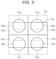
- FIG. 3 is an explanatory diagram illustrating the effective region of an image sensor.
- FIG. 4 is an explanatory diagram illustrating a graph of exemplary characteristics of blue, green, and red color filters corresponding to the three primary colors of light and exemplary characteristics of bandpass filters used in the sensor module according to the embodiment.
- FIG. 5 is an explanatory diagram illustrating an example of a bandpass filter.
- FIG. 6 is an explanatory diagram illustrating exemplary characteristics of a bandpass filter.
- FIG. 7 is an explanatory diagram illustrating exemplary characteristics of a bandpass filter.
- FIG. 8 is an explanatory diagram illustrating exemplary characteristics of a bandpass filter.
- FIG. 9 is an explanatory diagram illustrating exemplary characteristics of a bandpass filter.
- FIG. 10 is an explanatory diagram illustrating an exemplary functional configuration of an information processing device incorporating the sensor module according to the embodiment.
- FIG. 1 is an explanatory diagram illustrating an exemplary external appearance of the sensor module according to the embodiment of the present disclosure.
- FIG. 1 will be used to describe the exemplary external appearance of the sensor module according to the embodiment of the present disclosure.
- a sensor module 100 illustrated in FIG. 1 is a sensor module that may be installed in a portable device carried by a user, such as a smartphone, a tablet terminal, a game console, or a portable music player, for example.
- the sensor module 100 according to the embodiment of the present disclosure includes a housing 110 and a rigid flexible board 120 .
- Four lenses 111 a to 111 d are provided on the light-incident face of the housing 110 . Note that although the present embodiment illustrates an example in which four lenses of the sensor module 100 are provided, the present disclosure is not limited to such an example.
- the sensor module 100 is provided with a bandpass filter inside the housing 110 .
- an image sensor is formed on the rigid flexible board 120 .
- the bandpass filter is divided into four regions, and against light passing through each of the four lenses 111 a to 111 d , light of a predetermined wavelength band (frequency band) is passed via the bandpass filter, and that light is made to irradiate the image sensor.
- the sensor module 100 according to the present embodiment is capable of generating image data exposed by light of different wavelength bands (frequency bands) in a single imaging.
- FIG. 2 is an explanatory diagram illustrating an exploded perspective view of the internal structure of the sensor module according to the embodiment of the present disclosure.
- FIG. 2 will be used to describe the internal structure of the sensor module according to the embodiment of the present disclosure.
- the housing 110 is provided with four lenses 111 a to 111 d . Additionally, the interior of the housing 110 is divided into four regions 110 a to 110 d as illustrated in FIG. 2 .
- a bandpass filter 112 passes light of a predetermined frequency band wavelength band (frequency band) against light passing through the four lenses 111 a to 111 d .
- the bandpass filter 112 includes four bandpass filters 112 a to 112 d having respectively different pass patterns. Light that has passed through the lens 111 a passes through the bandpass filter 112 a .
- light that has passed through the lens 111 b passes through the bandpass filter 112 b
- light that has passed through the lens 111 c passes through the bandpass filter 112 c
- light that has passed through the lens 111 d passes through the bandpass filter 112 d .
- Light that has passed through the bandpass filter 112 is radiated onto an image sensor 121 .
- the image sensor 121 is an image sensor provided with a charge-coupled device (CCD) or complementary metal-oxide semiconductor (CMOS) imaging element, for example, and converts light that has passed through the bandpass filter 112 into an electric signal.
- CCD charge-coupled device
- CMOS complementary metal-oxide semiconductor
- the image sensor 121 is divided into four regions 121 a to 121 d , and respectively converts light that has passed through the bandpass filters 112 a to 112 d into electric signals.
- the image sensor 121 is provided with color filters on top of the imaging element.
- an effective region of the image sensor 121 refers to a region irradiated by light through a lens.
- FIG. 3 is an explanatory diagram illustrating effective regions of the image sensor 121 , and is a diagram illustrating the state of the sensor module 100 as viewed from the side on which the lenses 111 a to 111 d are provided. As illustrated in FIG. 3 , by providing the lenses 111 a to 111 d , four effective regions 122 a to 122 d exist on the image sensor 121 . The image sensor 121 generates image data by photoelectrically converting light radiated onto the effective regions 122 a to 122 d.
- pupil correction may also be performed such that incident light passing through the lenses 111 a to 111 d is made to irradiate the image sensor 121 efficiently.
- Pupil correction is a correction that adjusts the lenses 111 a to 111 d to match the angle of incidence of light rays in a central part and a peripheral part of the lenses 111 a to 111 d.
- the sensor module 100 is provided with the bandpass filter 112 that includes four bandpass filters 112 a to 112 d having different pass patterns.
- Each of the bandpass filters 112 a to 112 d is a bandpass filter that passes light of a predetermined range of wavelength bands while attenuating light of other wavelength bands, or alternatively is a combination of such bandpass filters.
- blue, green and red color filters corresponding to the three primary colors of light are provided in a Bayer array.
- the image sensor 121 of the present embodiment is characterized by being provided with a color filter having a different array for each region for extracting the component of a desired frequency band.
- FIG. 4 is an explanatory diagram illustrating a graph of exemplary characteristics of blue, green, and red color filters corresponding to the three primary colors of light and exemplary characteristics of bandpass filters used in the sensor module 100 according to the embodiment of the present disclosure.
- the sign 131 denotes the characteristics of the blue color filter
- the sign 132 denotes the characteristics of the green color filter
- the sign 133 denotes the characteristics of the red color filter.
- the signs 141 to 147 denote exemplary characteristics of bandpass filters used in the sensor module 100 according to the embodiment of the present disclosure.
- the bandpass filters used in the sensor module 100 are designated BPF 1 , BPF 2 , . . . , BPF 7 in order of shortest wavelength.
- the bandpass filters 112 a to 112 d have at least one from among BPF 1 to BPF 7 .
- 500 nm to 550 nm is a wavelength band in which the chlorophyll of vegetables and plants is easily visualized. Consequently, in the case of wanting to use the sensor module 100 for the purpose of visualizing the chlorophyll of vegetables and plants, it is desirable to create and incorporate into the sensor module 100 a bandpass including BPF 3 .
- 550 nm to 600 nm is a wavelength band in which metmyoglobin, a causative agent that turns brown as meat gets older, is easily visualized, and therefore is a wavelength band in which the deterioration of meat is easily visualized. Consequently, in the case of wanting to use the sensor module 100 for the purpose of visualizing the deterioration of meat, it is desirable to create and incorporate into the sensor module 100 a bandpass including BPF 4 .
- 600 nm to 650 nm is a wavelength band in which lycopene contained in tomatoes or the like is easily visualized. Consequently, in the case of wanting to use the sensor module 100 for the purpose of visualizing lycopene, it is desirable to create and incorporate into the sensor module 100 a bandpass including BPF 5 .
- 650 nm to 700 nm is a wavelength band in which components associated with the freshness of meat are easily visualized. Consequently, in the case of wanting to use the sensor module 100 for the purpose of visualizing components associated with the freshness of meat, it is desirable to create and incorporate into the sensor module 100 a bandpass including BPF 6 .
- 800 nm to 900 nm is a wavelength band in which the water content contained in vegetables and plants is easily visualized. Consequently, in the case of wanting to use the sensor module 100 for the purpose of visualizing the water content contained in vegetables and plants, it is desirable to create and incorporate into the sensor module 100 a bandpass including BPF 7 .
- the sensor module 100 is capable of accommodating these uses with a single sensor module 100 .
- the color filters provided in the image sensor 121 are treated as color filters in a Bayer array using the three primary colors of light, namely, blue, green, and red, color filters with low sensitivity to light that has passed through the bandpass filter 112 will exist.
- sensitivity is not obtained for wavelengths in the bands of 400 nm to 450 nm passed by BPF 1 and 600 nm to 650 nm passed by BPF 5 . Consequently, for regions in which BPF 1 or BPF 5 is provided, little to no information is obtained from the green pixels. Therefore, the green pixels are wasted.
- the sensor module 100 to separate the components of the seven frequency bands described above from light that has passed through each of the bandpass filters 112 a to 112 d and also efficiently obtain information about the light that has passed through the bandpass filters 112 a to 112 d , color filters that correspond to the frequency band passed by each of the bandpass filters 112 a to 112 d are provided in the image sensor 121 .
- color filters with an increased number of pixels from which information about light that has passed through the bandpass filters 112 a to 112 d is obtained are provided in the image sensor 121 .
- the sensor module 100 according to the present embodiment is capable of accommodating a variety of uses by changing the combination of bandpass filters. For example, in cases in which it is difficult to discriminate between a human face and an elaborately crafted doll or the face of a mannequin by simply performing image processing alone, the change in the spectral reflectance of skin around certain wavelengths may be utilized, and bandpass filters that transmit light of those wavelengths may be provided in the sensor module 100 . In this way, by providing bandpass filters that transmit the light of wavelengths at which the spectral reflectance of skin changes, the sensor module 100 according to the present embodiment may be used for biometric authentication.
- FIG. 5 is an explanatory diagram illustrating an example of bandpass filters configured as the bandpass filters 112 a to 112 d and color filters provided in the image sensor 121 in correspondence with each of the bandpass filters 112 a to 112 d .
- the bandpass filter 112 a includes BPF 1 and BPF 4 .
- the bandpass filter 112 b includes BPF 2 and BPF 5 .
- the bandpass filter 112 c includes BPF 3 and BPF 6 .
- the bandpass filter 112 d includes BPF 7 .
- the color filters provided in the image sensor 121 are formed such that the components of the frequency bands passed by each of the bandpass filters 112 a to 112 d are obtained. Since the bandpass filter 112 a includes BPF 1 and BPF 4 , in the region of the bandpass filter 112 a , pixels that pair with the blue color filter and pixels without a color filter (black-and-white pixels) are arranged in a check pattern. Since the bandpass filter 112 b includes BPF 2 and BPF 5 , in the region of the bandpass filter 112 b , pixels that pair with the red color filter and pixels that pair with the blue color filter are arranged in a check pattern.
- the bandpass filter 112 c includes BPF 3 and BPF 6 , in the region of the bandpass filter 112 c , pixels that pair with the green color filter and pixels that pair with the red color filter are arranged in a check pattern. Since the bandpass filter 112 d includes BPF 7 , in the region of the bandpass filter 112 c , pixels without a color filter (black-and-white pixels) are arranged.
- the sensor module 100 forms a pixel array capable of extracting the component of each frequency band efficiently. Furthermore, the sensor module 100 according to the present embodiment is capable of extracting, in a single imaging, the components of seven desired frequency bands with four types of bandpass filters and ordinary color filters using the three primary colors of light, namely blue, green, and red.
- FIGS. 6 to 9 are explanatory diagrams illustrating exemplary characteristics of the bandpass filter 112 a .
- the bandpass filter 112 a includes BPF 1 and BPF 4 , light in the wavelength bands as illustrated in FIG. 6 is passed, whereas light in other wavelength bands is attenuated.
- the bandpass filter 112 b includes BPF 2 and BPF 5 , light in the wavelength bands as illustrated in FIG. 7 is passed, whereas light in other wavelength bands is attenuated.
- the bandpass filter 112 c includes BPF 3 and BPF 6 , light in the wavelength bands as illustrated in FIG. 8 is passed, whereas light in other wavelength bands is attenuated.
- the bandpass filter 112 d includes BPF 7 , light in the wavelength band as illustrated in FIG. 9 is passed, whereas light in other wavelength bands is attenuated.
- the sensor module 100 By overlaying the four sorts of bandpass filters and color filters described above onto the single image sensor 121 , the sensor module 100 according to the present embodiment is capable of generating image data appropriate to at least four sorts of uses.
- the bandpass filter 112 a of the region 110 a includes BPF 1 and BPF 5
- the bandpass filter 112 b of the region 110 b includes BPF 2 and BPF 6
- the bandpass filter 112 c of the region 110 c includes BPF 3 and BPF 7
- the bandpass filter 112 d of the region 110 d includes BPF 4 .
- pixels that pair with the blue color filter and pixels that pair with the red color filter are arranged in a check pattern.
- pixels that pair with the blue color filter and pixels that pair with the red color filter are arranged in a check pattern.
- pixels that pair with the green color filter and pixels without a color filter are arranged in a check pattern.
- pixels without a color filter are arranged in the region of the bandpass filter 112 d .
- the sensor module 100 is capable of extracting, in a single imaging, the components of seven desired frequency bands with four types of bandpass filters and ordinary color filters using the three primary colors of light, namely blue, green, and red.
- the bandpass filter 112 a of the region 110 a includes BPF 1 and BPF 5
- the bandpass filter 112 b of the region 110 b includes BPF 2 and BPF 6
- the bandpass filter 112 c of the region 110 c includes BPF 3 and BPF 7
- the bandpass filter 112 d of the region 110 d includes BPF 4 .
- pixels that pair with the red color filter and pixels without a color filter are arranged in a check pattern.
- the component of the frequency band of BPF 5 can be extracted by the pixels that pair with the red color filter.
- the component of the frequency band of BPF 1 can be extracted by subtracting that which is obtained by the pixels that pair with the red color filter from that which is obtained by the pixels without a color filter (black-and-white pixels).
- pixels that pair with the blue color filter and pixels without a color filter are arranged in a check pattern.
- the component of the frequency band of BPF 2 can be extracted by the pixels that pair with the blue color filter.
- the component of the frequency band of BPF 6 can be extracted by subtracting that which is obtained by the pixels that pair with the blue color filter from that which is obtained by the pixels without a color filter (black-and-white pixels).
- pixels that pair with the green color filter and pixels without a color filter are arranged in a check pattern.
- the component of the frequency band of BPF 3 can be extracted by the pixels that pair with the green color filter.
- the component of the frequency band of BPF 7 can be extracted by the pixels without a color filter (black-and-white pixels).
- pixels without a color filter black-and-white pixels
- the component of the frequency band of BPF 4 can be extracted by the pixels without a color filter (black-and-white pixels).
- the sensor module 100 becomes capable of extracting the components of desired frequency bands efficiently.
- FIG. 10 is an explanatory diagram illustrating an exemplary functional configuration of an information processing device 1000 incorporating the sensor module 100 according to the embodiment of the present disclosure.
- the information processing device 1000 includes the sensor module 100 , an image processing unit 1010 , a control unit 1020 , a display unit 1030 , a communication unit 1040 , an input unit 1050 , and a storage unit 1060 .
- Image data generated by the sensor module 100 is sent to the image processing unit 1010 .
- the image processing unit 1010 includes a circuit that executes image processing, such as a graphics processing unit (GPU), and executes various types of image processing on the image data output by the sensor module 100 .
- the image processing unit 1010 performs noise removal, partitioning into image data of each of the regions 121 a to 121 d of the image sensor 121 , and the like.
- the image processing unit 1010 outputs the image-processed image data to the control unit 1020 .
- the control unit 1020 includes a central processing unit (CPU), a micro-processing unit (MPU), or the like, and controls the operations of the information processing device 1000 .
- CPU central processing unit
- MPU micro-processing unit
- the display unit 1030 includes a liquid crystal display or an organic EL display, for example.
- the display unit 1030 may also be provided with a touch panel that a user operates by touching a screen directly.
- the communication unit 1040 executes a process of communicating with another device by, for example, performing cellular communication, connecting to a wireless LAN or the like, or using a wireless communication standard such as infrared communication or Bluetooth (registered trademark).
- the input unit 1050 is a device for enabling the user to perform input operations, and may include for example a keyboard and mouse, a touch panel, or the like.
- the storage unit 1060 includes non-volatile or volatile memory, for example, holds programs and data necessary for operations of the information processing device 1000 , and stores logs of operations of the information processing device 1000 .
- FIG. 10 illustrates the information processing device 1000 incorporating only the sensor module 100 according to the embodiment of the present disclosure
- the present disclosure is not limited to such an example, and the information processing device 1000 may also incorporate a sensor module provided with color filters in an ordinary Bayer array in addition to the sensor module 100 .
- the information processing device 1000 by being provided with the sensor module 100 according to the embodiment of the present disclosure, is capable of obtaining image data to be used for a variety of purposes with a single imaging process.
- the information processing device 1000 provided with the sensor module 100 according to the embodiment of the present disclosure can be used to visualize the state of chlorophyll and water content in vegetables and plants or to visualize components associated with the deterioration and freshness of meat as described above.
- the sensor module 100 capable of generating image data exposed by light of different wavelength bands (frequency bands) in a single imaging process, as well as the information processing device 1000 provided with such a sensor module 100 .
- a solid-state imaging device including:
- a plurality of lenses configured to condense light
- a filter unit having a plurality of regions respectively irradiated by light passing through the plurality of lenses, the plurality of regions including transmission patterns configured to transmit different wavelength bands of the light;
- an image sensor in which pixels configured to convert light transmitted through the filter unit into electric signals are arranged in a matrix, the image sensor being provided with color filters that correspond to the transmission patterns on a filter-unit side of the pixels.
- the solid-state imaging device in which the transmission patterns are at least one selected from among bandpass filters configured to transmit respectively different wavelength bands.
- the solid-state imaging device in which the transmission patterns are two bandpass filters having non-adjacent wavelength bands selected from among the bandpass filters configured to transmit respectively different wavelength bands.
- the solid-state imaging device in which the wavelength bands transmitted by the bandpass filters are set in intervals of at least 50 nm.
- the solid-state imaging device according to any one of ( ) to (4), in which the color filters are formed in correspondence with each of the pixels of the image sensor.
- An information processing device including: the solid-state imaging device according to any one of (1) to (5).
Landscapes
- Physics & Mathematics (AREA)
- Engineering & Computer Science (AREA)
- Multimedia (AREA)
- Signal Processing (AREA)
- General Physics & Mathematics (AREA)
- Optics & Photonics (AREA)
- Color Television Image Signal Generators (AREA)
- Solid State Image Pick-Up Elements (AREA)
- Optical Filters (AREA)
Applications Claiming Priority (4)
| Application Number | Priority Date | Filing Date | Title |
|---|---|---|---|
| JP2017-084523 | 2017-04-21 | ||
| JPJP2017-084523 | 2017-04-21 | ||
| JP2017084523A JP6878111B2 (ja) | 2017-04-21 | 2017-04-21 | 固体撮像装置及び情報処理装置 |
| PCT/JP2018/007864 WO2018193727A1 (ja) | 2017-04-21 | 2018-03-01 | 固体撮像装置及び情報処理装置 |
Publications (2)
| Publication Number | Publication Date |
|---|---|
| US20200106994A1 US20200106994A1 (en) | 2020-04-02 |
| US11265520B2 true US11265520B2 (en) | 2022-03-01 |
Family
ID=63857130
Family Applications (1)
| Application Number | Title | Priority Date | Filing Date |
|---|---|---|---|
| US16/497,447 Active US11265520B2 (en) | 2017-04-21 | 2018-03-01 | Solid-state imaging device and information processing device |
Country Status (4)
| Country | Link |
|---|---|
| US (1) | US11265520B2 (de) |
| EP (1) | EP3614435B1 (de) |
| JP (1) | JP6878111B2 (de) |
| WO (1) | WO2018193727A1 (de) |
Citations (19)
| Publication number | Priority date | Publication date | Assignee | Title |
|---|---|---|---|---|
| US6222631B1 (en) * | 1998-01-08 | 2001-04-24 | Minolta Co., Ltd. | Two-dimensional spectral characteristic measuring apparatus |
| US20030086013A1 (en) | 2001-11-02 | 2003-05-08 | Michiharu Aratani | Compound eye image-taking system and apparatus with the same |
| US6611289B1 (en) * | 1999-01-15 | 2003-08-26 | Yanbin Yu | Digital cameras using multiple sensors with multiple lenses |
| US20070097249A1 (en) * | 2004-10-28 | 2007-05-03 | Tsuguhiro Korenaga | Camera module |
| JP2009164654A (ja) | 2006-04-24 | 2009-07-23 | Panasonic Corp | 複眼方式のカメラモジュール |
| US20100140461A1 (en) * | 2006-12-13 | 2010-06-10 | Georgia Tech Research Corporation | Systems and methods for real time multispectral imaging |
| JP2011022432A (ja) | 2009-07-17 | 2011-02-03 | Sony Corp | 多層膜光学フィルタ、固体撮像素子、撮像装置、表示装置、通信装置 |
| US8081311B2 (en) * | 2005-11-04 | 2011-12-20 | General Hospital Corporation | System for multispectral imaging |
| US20130331669A1 (en) * | 2012-06-11 | 2013-12-12 | Raytheon Company | Multi-spectral imaging system and method for remote biometric measurement of human physiological parameters |
| WO2015199163A1 (ja) | 2014-06-24 | 2015-12-30 | 日立マクセル株式会社 | 撮像センサおよび撮像装置 |
| US20150381907A1 (en) | 2014-06-26 | 2015-12-31 | Semiconductor Components Industries, Llc | Imaging systems for infrared and visible imaging with patterned infrared cutoff filters |
| US9258495B2 (en) * | 2012-06-21 | 2016-02-09 | Providence Photonics, Llc | Multi-spectral infrared imaging system for flare combustion efficiency monitoring |
| US20160094781A1 (en) * | 2013-06-06 | 2016-03-31 | Fujifilm Corporation | Auto-focus device and method for controlling operation of same |
| US20160099272A1 (en) | 2014-10-06 | 2016-04-07 | Visera Technologies Company Limited | Stacked filter and image sensor containing the same |
| US9972651B2 (en) * | 2015-08-03 | 2018-05-15 | Visera Technologies Company Limited | Spectrum-inspection device |
| US10051159B2 (en) * | 2014-07-31 | 2018-08-14 | Panasonic Intellectual Property Management Co., Ltd. | Imaging apparatus and imaging system |
| US20180292706A1 (en) * | 2017-04-11 | 2018-10-11 | Leica Instruments (Singapore) Pte. Ltd. | Multiple band pass liquid crystal tunable filter |
| US20190025482A1 (en) * | 2016-08-30 | 2019-01-24 | Samsung Electronics Co., Ltd. | Optical module and optical device using same |
| US20190363116A1 (en) * | 2016-11-20 | 2019-11-28 | Unispectral Ltd. | Multi-band imaging systems |
Family Cites Families (1)
| Publication number | Priority date | Publication date | Assignee | Title |
|---|---|---|---|---|
| US7920908B2 (en) * | 2003-10-16 | 2011-04-05 | David Hattery | Multispectral imaging for quantitative contrast of functional and structural features of layers inside optically dense media such as tissue |
-
2017
- 2017-04-21 JP JP2017084523A patent/JP6878111B2/ja not_active Expired - Fee Related
-
2018
- 2018-03-01 WO PCT/JP2018/007864 patent/WO2018193727A1/ja not_active Ceased
- 2018-03-01 EP EP18787756.8A patent/EP3614435B1/de active Active
- 2018-03-01 US US16/497,447 patent/US11265520B2/en active Active
Patent Citations (22)
| Publication number | Priority date | Publication date | Assignee | Title |
|---|---|---|---|---|
| US6222631B1 (en) * | 1998-01-08 | 2001-04-24 | Minolta Co., Ltd. | Two-dimensional spectral characteristic measuring apparatus |
| US6611289B1 (en) * | 1999-01-15 | 2003-08-26 | Yanbin Yu | Digital cameras using multiple sensors with multiple lenses |
| US20030086013A1 (en) | 2001-11-02 | 2003-05-08 | Michiharu Aratani | Compound eye image-taking system and apparatus with the same |
| JP2003143459A (ja) | 2001-11-02 | 2003-05-16 | Canon Inc | 複眼撮像系およびこれを備えた装置 |
| US20070097249A1 (en) * | 2004-10-28 | 2007-05-03 | Tsuguhiro Korenaga | Camera module |
| US8081311B2 (en) * | 2005-11-04 | 2011-12-20 | General Hospital Corporation | System for multispectral imaging |
| JP2009164654A (ja) | 2006-04-24 | 2009-07-23 | Panasonic Corp | 複眼方式のカメラモジュール |
| US20100140461A1 (en) * | 2006-12-13 | 2010-06-10 | Georgia Tech Research Corporation | Systems and methods for real time multispectral imaging |
| JP2011022432A (ja) | 2009-07-17 | 2011-02-03 | Sony Corp | 多層膜光学フィルタ、固体撮像素子、撮像装置、表示装置、通信装置 |
| US20130331669A1 (en) * | 2012-06-11 | 2013-12-12 | Raytheon Company | Multi-spectral imaging system and method for remote biometric measurement of human physiological parameters |
| US9258495B2 (en) * | 2012-06-21 | 2016-02-09 | Providence Photonics, Llc | Multi-spectral infrared imaging system for flare combustion efficiency monitoring |
| US20160094781A1 (en) * | 2013-06-06 | 2016-03-31 | Fujifilm Corporation | Auto-focus device and method for controlling operation of same |
| WO2015199163A1 (ja) | 2014-06-24 | 2015-12-30 | 日立マクセル株式会社 | 撮像センサおよび撮像装置 |
| US20170134704A1 (en) | 2014-06-24 | 2017-05-11 | Hitachi Maxell, Ltd. | Imaging processing device and imaging processing method |
| US20150381907A1 (en) | 2014-06-26 | 2015-12-31 | Semiconductor Components Industries, Llc | Imaging systems for infrared and visible imaging with patterned infrared cutoff filters |
| US10051159B2 (en) * | 2014-07-31 | 2018-08-14 | Panasonic Intellectual Property Management Co., Ltd. | Imaging apparatus and imaging system |
| US20160099272A1 (en) | 2014-10-06 | 2016-04-07 | Visera Technologies Company Limited | Stacked filter and image sensor containing the same |
| JP2016075886A (ja) | 2014-10-06 | 2016-05-12 | 采▲ぎょく▼科技股▲ふん▼有限公司VisEra Technologies Company Limited | スタックフィルターとそれを含むイメージセンサー |
| US9972651B2 (en) * | 2015-08-03 | 2018-05-15 | Visera Technologies Company Limited | Spectrum-inspection device |
| US20190025482A1 (en) * | 2016-08-30 | 2019-01-24 | Samsung Electronics Co., Ltd. | Optical module and optical device using same |
| US20190363116A1 (en) * | 2016-11-20 | 2019-11-28 | Unispectral Ltd. | Multi-band imaging systems |
| US20180292706A1 (en) * | 2017-04-11 | 2018-10-11 | Leica Instruments (Singapore) Pte. Ltd. | Multiple band pass liquid crystal tunable filter |
Non-Patent Citations (3)
| Title |
|---|
| Extended European Search Report dated Mar. 23, 2020, issued in corresponding European Patent Application No. 18787756.8. |
| International Search Report and Written Opinion dated May 1, 2018 for PCT/JP2018/007864 filed on Mar. 1, 2018, 10 pages including English Translation of the International Search Report. |
| Office Action dated Oct. 20, 2020, in corresponding Japanese patent Application No. 2017-084523, 12 pages. |
Also Published As
| Publication number | Publication date |
|---|---|
| JP2018182255A (ja) | 2018-11-15 |
| US20200106994A1 (en) | 2020-04-02 |
| JP6878111B2 (ja) | 2021-05-26 |
| EP3614435A4 (de) | 2020-04-22 |
| WO2018193727A1 (ja) | 2018-10-25 |
| EP3614435A1 (de) | 2020-02-26 |
| EP3614435B1 (de) | 2022-01-05 |
Similar Documents
| Publication | Publication Date | Title |
|---|---|---|
| US11134848B2 (en) | Mobile hyperspectral camera system and human skin monitoring using a mobile hyperspectral camera system | |
| CN103826530B (zh) | 摄像系统 | |
| JP2018107817A5 (de) | ||
| AU2025248641A1 (en) | Hybrid visible and near infrared imaging with an rgb color filter array sensor | |
| CN108769502A (zh) | 摄像处理装置以及摄像处理方法 | |
| US20180184039A1 (en) | Simultaneous Display of Two or More Different Sequentially Processed Images | |
| US12273634B2 (en) | Imaging element and electronic apparatus | |
| EP4307701A3 (de) | Bilderfassung mittels bayer-musterfilter mit mehreren bandpässen zur unterscheidung von lipid- und kollagengeweben | |
| JP2017059739A (ja) | 固体撮像装置および電子機器 | |
| CN111201770B (zh) | 电子仪器 | |
| CN114041085A (zh) | 摄像装置 | |
| CN111201771A (zh) | 电子仪器 | |
| US11265520B2 (en) | Solid-state imaging device and information processing device | |
| CN214231268U (zh) | 内窥镜成像装置和电子设备 | |
| US20160295116A1 (en) | Multi-functional displays | |
| WO2016174778A1 (ja) | 撮像装置、画像処理装置および画像処理方法 | |
| JP7830439B2 (ja) | 固体撮像装置及び電子機器 | |
| US20110080506A1 (en) | Image sensing device and system | |
| US11978278B2 (en) | Biometric imaging device comprising color filters and method of imaging using the biometric imaging device | |
| TWI428108B (zh) | 影像感測裝置及其處理系統 | |
| US20240161536A1 (en) | Biometric information acquiring apparatus | |
| KR20110135537A (ko) | 다중 스펙트럼 전자기파의 영상 촬영 시스템 및 다중 스펙트럼 전자기파의 영상 촬영 방법 | |
| JP2023152864A (ja) | 光学センサ装置のための隠蔽性要素 | |
| WO2024047944A1 (ja) | 校正用部材、筐体装置、校正装置、校正方法、及びプログラム | |
| CN121925964A (zh) | 成像元件、摄像装置、成像元件的控制方法及成像元件的控制程序 |
Legal Events
| Date | Code | Title | Description |
|---|---|---|---|
| AS | Assignment |
Owner name: SONY MOBILE COMMUNICATIONS INC., JAPAN Free format text: ASSIGNMENT OF ASSIGNORS INTEREST;ASSIGNOR:HASEGAWA, MASAAKI;REEL/FRAME:050479/0841 Effective date: 20190910 |
|
| FEPP | Fee payment procedure |
Free format text: ENTITY STATUS SET TO UNDISCOUNTED (ORIGINAL EVENT CODE: BIG.); ENTITY STATUS OF PATENT OWNER: LARGE ENTITY |
|
| STPP | Information on status: patent application and granting procedure in general |
Free format text: NON FINAL ACTION MAILED |
|
| STPP | Information on status: patent application and granting procedure in general |
Free format text: RESPONSE TO NON-FINAL OFFICE ACTION ENTERED AND FORWARDED TO EXAMINER |
|
| STPP | Information on status: patent application and granting procedure in general |
Free format text: FINAL REJECTION MAILED |
|
| STPP | Information on status: patent application and granting procedure in general |
Free format text: DOCKETED NEW CASE - READY FOR EXAMINATION |
|
| STPP | Information on status: patent application and granting procedure in general |
Free format text: NON FINAL ACTION MAILED |
|
| STPP | Information on status: patent application and granting procedure in general |
Free format text: RESPONSE TO NON-FINAL OFFICE ACTION ENTERED AND FORWARDED TO EXAMINER |
|
| STPP | Information on status: patent application and granting procedure in general |
Free format text: NOTICE OF ALLOWANCE MAILED -- APPLICATION RECEIVED IN OFFICE OF PUBLICATIONS |
|
| STCF | Information on status: patent grant |
Free format text: PATENTED CASE |
|
| MAFP | Maintenance fee payment |
Free format text: PAYMENT OF MAINTENANCE FEE, 4TH YEAR, LARGE ENTITY (ORIGINAL EVENT CODE: M1551); ENTITY STATUS OF PATENT OWNER: LARGE ENTITY Year of fee payment: 4 |