US11252311B2 - Camera module - Google Patents

Camera module Download PDF

Info

Publication number
US11252311B2
US11252311B2 US16/750,344 US202016750344A US11252311B2 US 11252311 B2 US11252311 B2 US 11252311B2 US 202016750344 A US202016750344 A US 202016750344A US 11252311 B2 US11252311 B2 US 11252311B2
Authority
US
United States
Prior art keywords
image sensor
substrate
camera module
lens
disposed
Prior art date
Legal status (The legal status is an assumption and is not a legal conclusion. Google has not performed a legal analysis and makes no representation as to the accuracy of the status listed.)
Active, expires
Application number
US16/750,344
Other versions
US20200374426A1 (en
Inventor
Won Seo GU
Soo Gil SIN
Sang Jin Kim
Current Assignee (The listed assignees may be inaccurate. Google has not performed a legal analysis and makes no representation or warranty as to the accuracy of the list.)
Samsung Electro Mechanics Co Ltd
Original Assignee
Samsung Electro Mechanics Co Ltd
Priority date (The priority date is an assumption and is not a legal conclusion. Google has not performed a legal analysis and makes no representation as to the accuracy of the date listed.)
Filing date
Publication date
Application filed by Samsung Electro Mechanics Co Ltd filed Critical Samsung Electro Mechanics Co Ltd
Assigned to SAMSUNG ELECTRO-MECHANICS CO., LTD. reassignment SAMSUNG ELECTRO-MECHANICS CO., LTD. ASSIGNMENT OF ASSIGNORS INTEREST (SEE DOCUMENT FOR DETAILS). Assignors: GU, WON SEO, KIM, SANG JIN, SIN, SOO GIL
Publication of US20200374426A1 publication Critical patent/US20200374426A1/en
Priority to US17/567,646 priority Critical patent/US11706510B2/en
Application granted granted Critical
Publication of US11252311B2 publication Critical patent/US11252311B2/en
Active legal-status Critical Current
Adjusted expiration legal-status Critical

Links

Images

Classifications

    • H04N5/2253
    • HELECTRICITY
    • H04ELECTRIC COMMUNICATION TECHNIQUE
    • H04NPICTORIAL COMMUNICATION, e.g. TELEVISION
    • H04N23/00Cameras or camera modules comprising electronic image sensors; Control thereof
    • H04N23/50Constructional details
    • H04N23/54Mounting of pick-up tubes, electronic image sensors, deviation or focusing coils
    • HELECTRICITY
    • H04ELECTRIC COMMUNICATION TECHNIQUE
    • H04NPICTORIAL COMMUNICATION, e.g. TELEVISION
    • H04N23/00Cameras or camera modules comprising electronic image sensors; Control thereof
    • H04N23/50Constructional details
    • HELECTRICITY
    • H04ELECTRIC COMMUNICATION TECHNIQUE
    • H04NPICTORIAL COMMUNICATION, e.g. TELEVISION
    • H04N23/00Cameras or camera modules comprising electronic image sensors; Control thereof
    • H04N23/50Constructional details
    • H04N23/55Optical parts specially adapted for electronic image sensors; Mounting thereof
    • H04N5/2254
    • HELECTRICITY
    • H05ELECTRIC TECHNIQUES NOT OTHERWISE PROVIDED FOR
    • H05KPRINTED CIRCUITS; CASINGS OR CONSTRUCTIONAL DETAILS OF ELECTRIC APPARATUS; MANUFACTURE OF ASSEMBLAGES OF ELECTRICAL COMPONENTS
    • H05K1/00Printed circuits
    • H05K1/02Details
    • H05K1/11Printed elements for providing electric connections to or between printed circuits
    • H05K1/115Via connections; Lands around holes or via connections
    • HELECTRICITY
    • H05ELECTRIC TECHNIQUES NOT OTHERWISE PROVIDED FOR
    • H05KPRINTED CIRCUITS; CASINGS OR CONSTRUCTIONAL DETAILS OF ELECTRIC APPARATUS; MANUFACTURE OF ASSEMBLAGES OF ELECTRICAL COMPONENTS
    • H05K3/00Apparatus or processes for manufacturing printed circuits
    • H05K3/30Assembling printed circuits with electric components, e.g. with resistor
    • H05K3/32Assembling printed circuits with electric components, e.g. with resistor electrically connecting electric components or wires to printed circuits
    • H05K3/321Assembling printed circuits with electric components, e.g. with resistor electrically connecting electric components or wires to printed circuits by conductive adhesives

Definitions

  • the present disclosure relates to a camera module.
  • a camera module may include an optical imaging system including one or more lenses and an image sensor.
  • the optical imaging system may include one or more lenses having refractive power, and may form an image of light reflected from a subject with the image sensor.
  • the image sensor may convert an optical signal refracted by the optical imaging system into an electrical signal.
  • Optical performance of the camera module is affected by a distance from the optical imaging system to the image sensor. For example, when a distance from the rearmost lens (a lens closest to the image sensor) of the optical imaging system to the image sensor is different from an optical design value or a rear focal length of the optical imaging system, an accurate image of the subject is not formed on an imaging plane of the image sensor.
  • the image sensor may be fixed to a substrate using an adhesive, and a position of the image sensor may thus be changed in a process of curing the adhesive.
  • a camera module in one general aspect, includes a lens, an image sensor disposed on a substrate and converting an optical signal refracted by the lens into an electrical signal, an adhesive member disposed between the substrate and the image sensor to fix the image sensor to the substrate, and a support member disposed between the substrate and the image sensor configured to maintain a constant distance between the lens and the image sensor even at a time of shrinkage-deformation of the adhesive member.
  • the support member may be disposed along a lower edge of the image sensor.
  • the adhesive member may be partially disposed in a diagonal direction of the image sensor.
  • the support member may have a bonding wire form.
  • the bonding wire may include a horizontal portion in line contact with a lower portion of the image sensor.
  • a camera module in another general aspect, includes a lens, a substrate having a groove, an image sensor disposed in the groove and converting an optical signal refracted by the lens into an electrical signal, an adhesive member fixing the image sensor to the groove, and a support member disposed in the groove configured to maintain a constant distance between the lens and the image sensor even at a time of shrinkage-deformation of the adhesive member.
  • the adhesive member may be disposed between inner surfaces of the groove and side surfaces of the image sensor.
  • the substrate may include a first substrate member in which a through-hole corresponding to the groove is formed, and a second substrate member coupled to the first substrate member and closing a lower portion of the through-hole.
  • a camera module in another general aspect, includes a substrate, a support member disposed on the substrate, an image sensor disposed on the support member, and an adhesive member bonded to the substrate and the image sensor, wherein the adhesive member thickness in a direction from the substrate to the image sensor is predetermined by the image sensor disposed against the support member.
  • the camera module may further include a lens configured to refract light including an optical signal converted by the image sensor to an electrical signal.
  • the support member may be spaced apart from the adhesive member.
  • the image sensor may be disposed on a bottom surface of a groove in the substrate, and the adhesive member may be further disposed on a side surface of the image sensor between inner surfaces of the groove.
  • the adhesive member may urge the image sensor against the support member.
  • the support member may include a plastically deformed portion to align the image sensor and the lens by a predetermined distance.
  • FIG. 1 is a cross-sectional view of a camera module according to one or more examples.
  • FIG. 2 is an enlarged view of part A illustrated in FIG. 1 .
  • FIG. 3 is a cross-sectional view taken along line B-B of FIG. 2 .
  • FIG. 4 is a cross-sectional view of a camera module according to one or more other examples.
  • FIG. 5 is an enlarged view of part D illustrated in FIG. 4 .
  • FIG. 6 is a cross-sectional view of a camera module according one or more still other examples.
  • FIG. 7 is an enlarged view of part E illustrated in FIG. 6 .
  • FIG. 8 is a cross-sectional view of a camera module according one or more still other examples.
  • FIG. 9 is an enlarged view of part F illustrated in FIG. 8 .
  • the term “and/or” includes any one and any combination of any two or more of the associated listed items; likewise, “at least one of” includes any one and any combination of any two or more of the associated listed items.
  • first,” “second,” and “third” may be used herein to describe various members, components, regions, layers, or sections, these members, components, regions, layers, or sections are not to be limited by these terms. Rather, these terms are only used to distinguish one member, component, region, layer, or section from another member, component, region, layer, or section. Thus, a first member, component, region, layer, or section referred to in examples described herein may also be referred to as a second member, component, region, layer, or section without departing from the teachings of the examples.
  • spatially relative terms such as “above,” “upper,” “below,” and “lower” may be used herein for ease of description to describe one element's relationship to another element as shown in the figures. Such spatially relative terms are intended to encompass different orientations of the device in use or operation in addition to the orientation depicted in the figures. For example, if the device in the figures is turned over, an element described as being “above” or “upper” relative to another element will then be “below” or “lower” relative to the other element. Thus, the term “above” encompasses both the above and below orientations depending on the spatial orientation of the device.
  • the device may also be oriented in other ways (for example, rotated 90 degrees or at other orientations), and the spatially relative terms used herein are to be interpreted accordingly.
  • One or more examples of a camera module in which a distance from the rearmost lens of an optical imaging system to an image sensor is accurately maintained are described herein.
  • a camera module according to the present disclosure may be configured so that a distance between a lens and an image sensor is constantly maintained.
  • the camera module according to the present disclosure may include support members disposed between the image sensor and a substrate. The support members may constantly maintain a relative position of the image sensor to the lens even at a time of shrinkage-deformation of an adhesive applied to a lower portion of the image sensor.
  • the support member may be formed of a material that is easily plastically-deformed.
  • the support member may be formed of a material that is a metal and is easily deformed, such as a bonding wire.
  • the support member formed as described above may enable adjustment of the relative position of the image sensor to the lens.
  • FIGS. 1 through 3 a camera module according to one or more examples will be described with reference to FIGS. 1 through 3 .
  • a camera module 10 may include an optical imaging system 100 , a substrate 200 , and an image sensor 300 .
  • the camera module 10 may further include an adhesive member 400 and support members 500 .
  • the optical imaging system 100 may include one or more lenses.
  • the optical imaging system 100 according to the present example may include a first lens 110 , a second lens 120 , and a third lens 130 .
  • the number of lenses constituting the optical imaging system 100 is not limited to three.
  • the optical imaging system 100 may include two or less or four or more lenses.
  • the optical imaging system 100 may have a focal length.
  • the optical imaging system 100 may have a predetermined back focal length (BF).
  • the optical imaging system 100 may further include a filter (not illustrated) for cutting off an infrared ray. In this case, the filter may be disposed between the rearmost lens (the third lens 130 in the present example) and the image sensor 300 .
  • the first lens 110 may have positive refractive power.
  • An object-side surface of the first lens 110 may be convex, and an image-side surface thereof may be convex.
  • the first lens 110 may have an aspherical surface.
  • at least one of the object-side surface and the image-side surface of the first lens 110 may be aspherical.
  • the second lens 120 may have positive refractive power.
  • An object-side surface of the second lens 120 may be concave, and an image-side surface thereof may be convex.
  • the second lens 120 may have an aspherical surface.
  • at least one of the object-side surface and the image-side surface of the second lens 120 may be aspherical.
  • the third lens 130 may have positive or negative refractive power.
  • An object-side surface of the third lens 130 may be concave, and an image-side surface thereof may be convex.
  • the third lens 130 may have an aspherical surface.
  • at least one of the object-side surface and the image-side surface of the third lens 130 may be aspherical.
  • connection pads for electrical connection to the electronic components may be formed on the substrate 200 .
  • the substrate 200 may electrically connect the electronic components mounted thereon to each other.
  • circuits for connecting the connection pads to each other may be formed on the substrate 200 .
  • the circuits may be formed on a surface of and inside the substrate 200 .
  • the image sensor 300 may be disposed on the substrate 200 .
  • the image sensor 300 may be disposed above the substrate 200 .
  • the image sensor 300 may convert an optical signal refracted by the optical imaging system 100 into an electrical signal.
  • the adhesive member 400 may be formed between the substrate 200 and the image sensor 300 .
  • the adhesive member 400 may be partially formed in a diagonal direction of the substrate 200 or the image sensor 300 , as illustrated in FIG. 3 .
  • the adhesive member 400 may be formed from a central portion of the substrate 200 or the image sensor 300 along width and length directions of the substrate 200 or the image sensor 300 .
  • the adhesive member 400 formed as described above may be photo-cured or thermally cured to firmly fix the image sensor 300 to the substrate 200 .
  • the support members 500 may be formed on the substrate 200 .
  • the support members 500 may be formed at intervals along a lower edge of the image sensor 300 as illustrated in FIG. 3 .
  • the support member 500 may have a bonding wire form.
  • the support members 500 formed as described above may be rapidly and easily formed in a wire bonding process of electrically connecting the substrate 200 and the electronic components to each other.
  • the support members 500 may support the image sensor 300 at a first height h 1 .
  • the first height h 1 may be in a range of approximately 110 to 140 ⁇ m.
  • the support members 500 may be formed between the substrate 200 and the image sensor 300 to maintain a constant distance (that is, a back focal length BF) between the optical imaging system 100 and the image sensor 300 .
  • the support members 500 may solve a phenomenon in which a distance between the substrate 200 and the image sensor 300 is decreased and the distance between the optical imaging system 100 and the image sensor 300 is increased due to shrinkage-curing of the adhesive member 400 .
  • a camera module according to one or more other examples will be described with reference to FIGS. 4 and 5 .
  • a camera module 20 may include an optical imaging system 100 , a substrate 200 , and an image sensor 300 .
  • the camera module 20 may further include an adhesive member 400 and support members 500 .
  • the optical imaging system 100 may include one or more lenses.
  • the optical imaging system 100 according to the present example may include a first lens 110 , a second lens 120 , and a third lens 130 .
  • the optical imaging system 100 may have a focal length.
  • the optical imaging system 100 may have a predetermined back focal length (BF).
  • the first lens 110 may have positive refractive power.
  • An object-side surface of the first lens 110 may be convex, and an image-side surface thereof may be concave.
  • the first lens 110 may have an aspherical surface.
  • at least one of the object-side surface and the image-side surface of the first lens 110 may be aspherical.
  • the second lens 120 may have positive or negative refractive power.
  • An object-side surface of the second lens 120 may be convex, and an image-side surface thereof may be concave.
  • the second lens 120 may have an aspherical surface.
  • at least one of the object-side surface and the image-side surface of the second lens 120 may be aspherical.
  • the third lens 130 may have positive or negative refractive power.
  • An object-side surface of the third lens 130 may be concave, and an image-side surface thereof may be convex.
  • the third lens 130 may have an aspherical surface.
  • at least one of the object-side surface and the image-side surface of the third lens 130 may be aspherical.
  • connection pads for electrical connection to the electronic components may be formed on the substrate 200 .
  • the substrate 200 may electrically connect the electronic components mounted thereon to each other.
  • circuits for connecting the connection pads to each other may be formed on the substrate 200 .
  • the circuits may be formed on a surface of and inside the substrate 200 .
  • the image sensor 300 may be disposed on the substrate 200 .
  • the image sensor 300 may be disposed above the substrate 200 .
  • the image sensor 300 may convert an optical signal refracted by the optical imaging system 100 into an electrical signal.
  • the adhesive member 400 may be formed between the substrate 200 and the image sensor 300 .
  • the adhesive member 400 may be partially formed in a diagonal direction of the substrate 200 or the image sensor 300 , as illustrated in FIG. 3 .
  • the adhesive member 400 may be formed from a central portion of the substrate 200 or the image sensor 300 along width and length directions of the substrate 200 or the image sensor 300 .
  • the adhesive member 400 formed as described above may be photo-cured or thermally cured to firmly fix the image sensor 300 to the substrate 200 .
  • the support members 500 may be formed on the substrate 200 .
  • the support members 500 may be formed at intervals along a lower edge of the image sensor 300 or a diagonal length direction of the image sensor 300 .
  • the support member 500 may have a bonding wire form.
  • the support members 500 formed as described above may be rapidly and easily formed in a wire bonding process of electrically connecting the substrate 200 and the electronic components to each other.
  • the support member 500 according to the present example may be configured in a bonding wire form having a horizontal portion 510 .
  • the support member 500 having such a form may be formed by pressing a bonding wire having a curved shape with a predetermined force.
  • a bonding wire having the horizontal portion 510 may be formed by pressing the image sensor 300 in a state in which the image sensor 300 is put on the support member 500 .
  • the support member 500 is formed by the latter method, a distance decrease phenomenon between the optical imaging system 100 and the image sensor 300 due to excessive application of the adhesive member 400 may be solved.
  • the horizontal portion 510 formed as described above may be in line contact with a lower portion of the image sensor 300 to firmly support the image sensor 300 .
  • the support members 500 may support the image sensor 300 at a second height h 2 that is significantly low.
  • the second height h 2 may be in a range of approximately 50 to 70 ⁇ m.
  • the support members 500 may be formed between the substrate 200 and the image sensor 300 to maintain a constant distance (that is, a back focal length BF) between the optical imaging system 100 and the image sensor 300 .
  • the support members 500 may solve a phenomenon in which a distance between the substrate 200 and the image sensor 300 is decreased and the distance between the optical imaging system 100 and the image sensor 300 is increased due to shrinkage-curing of the adhesive member 400 .
  • a camera module according to one or more other examples will be described with reference to FIGS. 6 and 7 .
  • a camera module 30 may include an optical imaging system 100 , a substrate 200 , and an image sensor 300 .
  • the camera module 30 may further include an adhesive member 400 and support members 500 .
  • the optical imaging system 100 may include one or more lenses.
  • the optical imaging system 100 according to the present example may include a first lens 110 , a second lens 120 , and a third lens 130 .
  • the optical imaging system 100 may have a focal length.
  • the optical imaging system 100 may have a predetermined back focal length (BF).
  • the first lens 110 may have positive refractive power.
  • An object-side surface of the first lens 110 may be convex, and an image-side surface thereof may be concave.
  • the first lens 110 may have an aspherical surface.
  • at least one of the object-side surface and the image-side surface of the first lens 110 may be aspherical.
  • the second lens 120 may have positive or negative refractive power.
  • An object-side surface of the second lens 120 may be concave, and an image-side surface thereof may be convex.
  • the second lens 120 may have an aspherical surface.
  • at least one of the object-side surface and the image-side surface of the second lens 120 may be aspherical.
  • the third lens 130 may have positive or negative refractive power.
  • An object-side surface of the third lens 130 may be concave, and an image-side surface thereof may be convex.
  • the third lens 130 may have an aspherical surface.
  • at least one of the object-side surface and the image-side surface of the third lens 130 may be aspherical.
  • connection pads for electrical connection to the electronic components may be formed on the substrate 200 .
  • the substrate 200 may electrically connect the electronic components mounted thereon to each other.
  • circuits for connecting the connection pads to each other may be formed on the substrate 200 .
  • the circuits may be formed on a surface of and inside the substrate 200 .
  • the substrate 200 may include a groove 202 accommodating the image sensor 300 therein.
  • the groove 202 may be formed at a significant depth Dp.
  • the depth Dp of the groove 202 may be substantially the same as a height h of the image sensor 300 .
  • the depth Dp of the groove 202 is not necessarily the same as the height h of the image sensor 300 .
  • the image sensor 300 may be disposed in the groove 202 of the substrate 200 .
  • the image sensor 300 may convert an optical signal refracted by the optical imaging system 100 into an electrical signal.
  • the adhesive member 400 may be formed between the substrate 200 and the image sensor 300 .
  • the adhesive member 400 may be formed between inner surfaces of the groove 202 and side surfaces of the image sensor 300 , as illustrated in FIG. 7 .
  • a position of the adhesive member 400 is not limited to the portion described above.
  • the adhesive member 400 may be formed between a bottom surface of the groove 202 and a lower portion of the image sensor 300 .
  • the adhesive member 400 formed as described above may be photo-cured or thermally cured to firmly fix the image sensor 300 to the substrate 200 .
  • the support members 500 may be formed on the substrate 200 .
  • the support members 500 may be formed at intervals along a lower edge of the image sensor 300 or a diagonal length direction of the image sensor 300 .
  • the support member 500 may have a bonding wire form.
  • the support members 500 formed as described above may be rapidly and easily formed in a wire bonding process of electrically connecting the substrate 200 and the electronic components to each other.
  • the support member 500 according to the present example may be configured in a bonding wire form having a horizontal portion 510 .
  • the support member 500 having such a form may be formed by pressing a bonding wire having a curved shape with a predetermined force.
  • a bonding wire having the horizontal portion 510 may be formed by pressing the image sensor 300 in a state in which the image sensor 300 is put on the support member 500 .
  • the support member 500 is formed by the latter method, a distance decrease phenomenon between the optical imaging system 100 and the image sensor 300 due to excessive application of the adhesive member 400 may be solved.
  • the horizontal portion 510 formed as described above may be in line contact with a lower portion of the image sensor 300 to firmly support the image sensor 300 .
  • the support members 500 may support the image sensor 300 at a second height h 2 that is significantly low.
  • the second height h 2 may be in a range of approximately 50 to 70 ⁇ m.
  • the support members 500 may be formed between the substrate 200 and the image sensor 300 to maintain a constant distance (that is, a back focal length BF) between the optical imaging system 100 and the image sensor 300 .
  • the support members 500 may solve a phenomenon in which a distance between the substrate 200 and the image sensor 300 is decreased and the distance between the optical imaging system 100 and the image sensor 300 is increased due to shrinkage-curing of the adhesive member 400 .
  • the image sensor 300 may be disposed in the groove 202 of the substrate 200 , such that an entire height of the camera module 30 may be decreased.
  • a camera module according to one or more other examples will be described with reference to FIGS. 8 and 9 .
  • a camera module 40 may include an optical imaging system 100 , a substrate 200 , and an image sensor 300 .
  • the camera module 40 may further include an adhesive member 400 and support members 500 .
  • the optical imaging system 100 may include one or more lenses.
  • the optical imaging system 100 according to the present example may include a first lens 110 , a second lens 120 , and a third lens 130 .
  • the optical imaging system 100 may have a focal length.
  • the optical imaging system 100 may have a predetermined back focal length (BF).
  • the first lens 110 may have positive refractive power.
  • An object-side surface of the first lens 110 may be convex, and an image-side surface thereof may be convex.
  • the first lens 110 may have an aspherical surface.
  • at least one of the object-side surface and the image-side surface of the first lens 110 may be aspherical.
  • the second lens 120 may have positive or negative refractive power.
  • An object-side surface of the second lens 120 may be concave, and an image-side surface thereof may be convex.
  • the second lens 120 may have an aspherical surface.
  • at least one of the object-side surface and the image-side surface of the second lens 120 may be aspherical.
  • the third lens 130 may have positive or negative refractive power.
  • An object-side surface of the third lens 130 may be concave, and an image-side surface thereof may be concave.
  • the third lens 130 may have an aspherical surface.
  • at least one of the object-side surface and the image-side surface of the third lens 130 may be aspherical.
  • the substrate 200 may include a plurality of members.
  • the substrate 200 may include a first substrate member 210 and a second substrate member 220 .
  • a through-hole 212 in which the image sensor 300 may be disposed may be formed in the first substrate member 210 .
  • the through-hole 212 may have a shape substantially similar to that of the image sensor 300 .
  • the through-hole 212 may have a substantially rectangular cross-sectional shape, similar to the image sensor 300 .
  • a cross section of the through-hole 212 may be substantially greater than that of the image sensor 300 .
  • a depth of the through-hole 212 may be substantially same as a height of the image sensor 300 . However, the depth of the through-hole 212 is not necessarily the same as the height of the image sensor 300 .
  • the second substrate member 220 may be disposed beneath the first substrate member 210 .
  • the second substrate member 220 may be formed at a size that is substantially the same as that of the first substrate member 210 .
  • the second substrate member 220 may close the through-hole 212 of the first substrate member 210 .
  • the second substrate member 220 may be attached to a lower portion of the first substrate member 210 in a process of manufacturing the adhesive member 400 or the substrate 200 .
  • the image sensor 300 may be disposed in the through-hole 212 of the first substrate member 210 .
  • the image sensor 300 may convert an optical signal refracted by the optical imaging system 100 into an electrical signal.
  • the adhesive member 400 may be formed between the substrate 200 and the image sensor 300 .
  • the adhesive member 400 may be formed between the second substrate member 220 and the image sensor 300 , as illustrated in FIG. 9 .
  • the adhesive member 400 formed as described above may be photo-cured or thermally cured to firmly fix the image sensor 300 to the substrate 200 .
  • a portion of the one or more electronic components described above as mounted on the substrate 200 may be mounted on the second substrate member 220 .
  • the support members 500 may be formed on the second substrate member 220 .
  • the support members 500 may be formed at intervals along a lower edge of the image sensor 300 or a diagonal length direction of the image sensor 300 .
  • the support member 500 may have a bonding wire form.
  • the support members 500 formed as described above may be rapidly and easily formed in a wire bonding process of electrically connecting the second substrate member 220 and the electronic components to each other.
  • the support member 500 according to the present example may be configured in a bonding wire form having a horizontal portion 510 .
  • the support member 500 having such a form may be formed by pressing a bonding wire having a curved shape with a predetermined force.
  • a bonding wire having the horizontal portion 510 may be formed by pressing the image sensor 300 in a state in which the image sensor 300 is put on the support member 500 .
  • the support member 500 is formed by the latter method, a distance decrease phenomenon between the optical imaging system 100 and the image sensor 300 due to excessive application of the adhesive member 400 may be solved.
  • the horizontal portion 510 formed as described above may be in line contact with a lower portion of the image sensor 300 to firmly support the image sensor 300 .
  • the support members 500 may support the image sensor 300 at a second height h 2 that is significantly low.
  • the second height h 2 may be in a range of approximately 50 to 70 ⁇ m.
  • the support members 500 may be formed between the substrate 200 and the image sensor 300 to maintain a constant distance (that is, a back focal length BF) between the optical imaging system 100 and the image sensor 300 .
  • the support members 500 may solve a phenomenon in which a distance between the substrate 200 and the image sensor 300 is decreased and the distance between the optical imaging system 100 and the image sensor 300 is increased due to shrinkage-curing of the adhesive member 400 .
  • the image sensor 300 may be disposed in the groove 212 of the first substrate member 210 , such that an entire height of the camera module 40 may be decreased.

Abstract

A camera module includes a lens; an image sensor disposed on a substrate and converting an optical signal refracted by the lens into an electrical signal, an adhesive member disposed between the substrate and the image sensor to fix the image sensor to the substrate, and a support member disposed between the substrate and the image sensor configured to maintain a constant distance between the lens and the image sensor even at a time of shrinkage-deformation of the adhesive member.

Description

CROSS-REFERENCE TO RELATED APPLICATIONS
This application claims the benefit under 35 USC 119(a) of Korean Patent Application No. 10-2019-0058814 filed on May 20, 2019, in the Korean Intellectual Property Office, the entire disclosure of which is incorporated herein by reference for all purposes.
BACKGROUND 1. Field
The present disclosure relates to a camera module.
2. Description of the Background
A camera module may include an optical imaging system including one or more lenses and an image sensor. The optical imaging system may include one or more lenses having refractive power, and may form an image of light reflected from a subject with the image sensor. The image sensor may convert an optical signal refracted by the optical imaging system into an electrical signal.
Optical performance of the camera module is affected by a distance from the optical imaging system to the image sensor. For example, when a distance from the rearmost lens (a lens closest to the image sensor) of the optical imaging system to the image sensor is different from an optical design value or a rear focal length of the optical imaging system, an accurate image of the subject is not formed on an imaging plane of the image sensor.
However, in a camera module, the image sensor may be fixed to a substrate using an adhesive, and a position of the image sensor may thus be changed in a process of curing the adhesive.
The above information is presented as background information only to assist with an understanding of the present disclosure. No determination has been made, and no assertion is made, as to whether any of the above might be applicable as prior art with regard to the disclosure.
SUMMARY
This Summary is provided to introduce a selection of concepts in a simplified form that are further described below in the Detailed Description. This Summary is not intended to identify key features or essential features of the claimed subject matter, nor is it intended to be used as an aid in determining the scope of the claimed subject matter.
In one general aspect, a camera module includes a lens, an image sensor disposed on a substrate and converting an optical signal refracted by the lens into an electrical signal, an adhesive member disposed between the substrate and the image sensor to fix the image sensor to the substrate, and a support member disposed between the substrate and the image sensor configured to maintain a constant distance between the lens and the image sensor even at a time of shrinkage-deformation of the adhesive member.
The support member may be disposed along a lower edge of the image sensor.
The adhesive member may be partially disposed in a diagonal direction of the image sensor.
The support member may have a bonding wire form.
The bonding wire may include a horizontal portion in line contact with a lower portion of the image sensor.
In another general aspect, a camera module includes a lens, a substrate having a groove, an image sensor disposed in the groove and converting an optical signal refracted by the lens into an electrical signal, an adhesive member fixing the image sensor to the groove, and a support member disposed in the groove configured to maintain a constant distance between the lens and the image sensor even at a time of shrinkage-deformation of the adhesive member.
The adhesive member may be disposed between inner surfaces of the groove and side surfaces of the image sensor.
The substrate may include a first substrate member in which a through-hole corresponding to the groove is formed, and a second substrate member coupled to the first substrate member and closing a lower portion of the through-hole.
In another general aspect, a camera module includes a substrate, a support member disposed on the substrate, an image sensor disposed on the support member, and an adhesive member bonded to the substrate and the image sensor, wherein the adhesive member thickness in a direction from the substrate to the image sensor is predetermined by the image sensor disposed against the support member.
The camera module may further include a lens configured to refract light including an optical signal converted by the image sensor to an electrical signal.
The support member may be spaced apart from the adhesive member.
The image sensor may be disposed on a bottom surface of a groove in the substrate, and the adhesive member may be further disposed on a side surface of the image sensor between inner surfaces of the groove.
The adhesive member may urge the image sensor against the support member.
The support member may include a plastically deformed portion to align the image sensor and the lens by a predetermined distance.
Other features and aspects will be apparent from the following detailed description, the drawings, and the claims.
BRIEF DESCRIPTION OF DRAWINGS
FIG. 1 is a cross-sectional view of a camera module according to one or more examples.
FIG. 2 is an enlarged view of part A illustrated in FIG. 1.
FIG. 3 is a cross-sectional view taken along line B-B of FIG. 2.
FIG. 4 is a cross-sectional view of a camera module according to one or more other examples.
FIG. 5 is an enlarged view of part D illustrated in FIG. 4.
FIG. 6 is a cross-sectional view of a camera module according one or more still other examples.
FIG. 7 is an enlarged view of part E illustrated in FIG. 6.
FIG. 8 is a cross-sectional view of a camera module according one or more still other examples.
FIG. 9 is an enlarged view of part F illustrated in FIG. 8.
Throughout the drawings and the detailed description, the same reference numerals refer to the same elements. The drawings may not be to scale, and the relative size, proportions, and depiction of elements in the drawings may be exaggerated for clarity, illustration, and convenience.
DETAILED DESCRIPTION
The following detailed description is provided to assist the reader in gaining a comprehensive understanding of the methods, apparatuses, and/or systems described herein. However, various changes, modifications, and equivalents of the methods, apparatuses, and/or systems described herein will be apparent after an understanding of this disclosure. For example, the sequences of operations described herein are merely examples, and are not limited to those set forth herein, but may be changed as will be apparent after an understanding of this disclosure, with the exception of operations necessarily occurring in a certain order. Also, descriptions of features that are known in the art may be omitted for increased clarity and conciseness.
The features described herein may be embodied in different forms, and are not to be construed as being limited to the examples described herein. Rather, the examples described herein have been provided merely to illustrate some of the many possible ways of implementing the methods, apparatuses, and/or systems described herein that will be apparent after an understanding of this disclosure. Hereinafter, while embodiments of the present disclosure will be described in detail with reference to the accompanying drawings, it is noted that examples are not limited to the same.
Throughout the specification, when an element, such as a layer, region, or substrate, is described as being “on,” “connected to,” or “coupled to” another element, it may be directly “on,” “connected to,” or “coupled to” the other element, or there may be one or more other elements intervening therebetween. In contrast, when an element is described as being “directly on,” “directly connected to,” or “directly coupled to” another element, there can be no other elements intervening therebetween.
As used herein, the term “and/or” includes any one and any combination of any two or more of the associated listed items; likewise, “at least one of” includes any one and any combination of any two or more of the associated listed items.
Although terms such as “first,” “second,” and “third” may be used herein to describe various members, components, regions, layers, or sections, these members, components, regions, layers, or sections are not to be limited by these terms. Rather, these terms are only used to distinguish one member, component, region, layer, or section from another member, component, region, layer, or section. Thus, a first member, component, region, layer, or section referred to in examples described herein may also be referred to as a second member, component, region, layer, or section without departing from the teachings of the examples.
Spatially relative terms such as “above,” “upper,” “below,” and “lower” may be used herein for ease of description to describe one element's relationship to another element as shown in the figures. Such spatially relative terms are intended to encompass different orientations of the device in use or operation in addition to the orientation depicted in the figures. For example, if the device in the figures is turned over, an element described as being “above” or “upper” relative to another element will then be “below” or “lower” relative to the other element. Thus, the term “above” encompasses both the above and below orientations depending on the spatial orientation of the device. The device may also be oriented in other ways (for example, rotated 90 degrees or at other orientations), and the spatially relative terms used herein are to be interpreted accordingly.
The terminology used herein is for describing various examples only, and is not to be used to limit the disclosure. The articles “a,” “an,” and “the” are intended to include the plural forms as well, unless the context clearly indicates otherwise. The terms “comprises,” “includes,” and “has” specify the presence of stated features, numbers, operations, members, elements, and/or combinations thereof, but do not preclude the presence or addition of one or more other features, numbers, operations, members, elements, and/or combinations thereof.
Due to manufacturing techniques and/or tolerances, variations of the shapes shown in the drawings may occur. Thus, the examples described herein are not limited to the specific shapes shown in the drawings, but include changes in shape that occur, for example, during manufacturing.
The features of the examples described herein may be combined in various ways as will be apparent after an understanding of this disclosure. Further, although the examples described herein have a variety of configurations, other configurations are possible as will be apparent after an understanding of this disclosure.
Herein, it is noted that use of the term “may” with respect to an example, for example, as to what an example may include or implement, means that at least one example exists in which such a feature is included or implemented while all examples are not limited thereto.
One or more examples of a camera module in which a distance from the rearmost lens of an optical imaging system to an image sensor is accurately maintained are described herein.
A camera module according to the present disclosure may be configured so that a distance between a lens and an image sensor is constantly maintained. For example, the camera module according to the present disclosure may include support members disposed between the image sensor and a substrate. The support members may constantly maintain a relative position of the image sensor to the lens even at a time of shrinkage-deformation of an adhesive applied to a lower portion of the image sensor.
The support member may be formed of a material that is easily plastically-deformed. For example, the support member may be formed of a material that is a metal and is easily deformed, such as a bonding wire. The support member formed as described above may enable adjustment of the relative position of the image sensor to the lens.
Hereinafter, various examples will be described with reference to the drawings.
First, a camera module according to one or more examples will be described with reference to FIGS. 1 through 3.
A camera module 10 according to the present example may include an optical imaging system 100, a substrate 200, and an image sensor 300. In addition, the camera module 10 may further include an adhesive member 400 and support members 500.
The optical imaging system 100 may include one or more lenses. For example, the optical imaging system 100 according to the present example may include a first lens 110, a second lens 120, and a third lens 130. However, the number of lenses constituting the optical imaging system 100 is not limited to three. For example, the optical imaging system 100 may include two or less or four or more lenses. The optical imaging system 100 may have a focal length. For example, the optical imaging system 100 may have a predetermined back focal length (BF). The optical imaging system 100 may further include a filter (not illustrated) for cutting off an infrared ray. In this case, the filter may be disposed between the rearmost lens (the third lens 130 in the present example) and the image sensor 300.
The first lens 110 may have positive refractive power. An object-side surface of the first lens 110 may be convex, and an image-side surface thereof may be convex. The first lens 110 may have an aspherical surface. For example, at least one of the object-side surface and the image-side surface of the first lens 110 may be aspherical. The second lens 120 may have positive refractive power. An object-side surface of the second lens 120 may be concave, and an image-side surface thereof may be convex. The second lens 120 may have an aspherical surface. For example, at least one of the object-side surface and the image-side surface of the second lens 120 may be aspherical. The third lens 130 may have positive or negative refractive power. An object-side surface of the third lens 130 may be concave, and an image-side surface thereof may be convex. The third lens 130 may have an aspherical surface. For example, at least one of the object-side surface and the image-side surface of the third lens 130 may be aspherical.
One or more electronic components may be mounted on the substrate 200. For example, connection pads for electrical connection to the electronic components may be formed on the substrate 200. The substrate 200 may electrically connect the electronic components mounted thereon to each other. For example, circuits for connecting the connection pads to each other may be formed on the substrate 200. The circuits may be formed on a surface of and inside the substrate 200.
The image sensor 300 may be disposed on the substrate 200. For example, the image sensor 300 may be disposed above the substrate 200. The image sensor 300 may convert an optical signal refracted by the optical imaging system 100 into an electrical signal.
The adhesive member 400 may be formed between the substrate 200 and the image sensor 300. For example, the adhesive member 400 may be partially formed in a diagonal direction of the substrate 200 or the image sensor 300, as illustrated in FIG. 3. In addition, the adhesive member 400 may be formed from a central portion of the substrate 200 or the image sensor 300 along width and length directions of the substrate 200 or the image sensor 300. The adhesive member 400 formed as described above may be photo-cured or thermally cured to firmly fix the image sensor 300 to the substrate 200.
The support members 500 may be formed on the substrate 200. For example, the support members 500 may be formed at intervals along a lower edge of the image sensor 300 as illustrated in FIG. 3. The support member 500 may have a bonding wire form. The support members 500 formed as described above may be rapidly and easily formed in a wire bonding process of electrically connecting the substrate 200 and the electronic components to each other. The support members 500 may support the image sensor 300 at a first height h1. Here, the first height h1 may be in a range of approximately 110 to 140 μm. In addition, the support members 500 may be formed between the substrate 200 and the image sensor 300 to maintain a constant distance (that is, a back focal length BF) between the optical imaging system 100 and the image sensor 300. For example, the support members 500 may solve a phenomenon in which a distance between the substrate 200 and the image sensor 300 is decreased and the distance between the optical imaging system 100 and the image sensor 300 is increased due to shrinkage-curing of the adhesive member 400.
Therefore, in the camera module 10 according to the present example, quality deterioration phenomenon of the camera module 10 due to the shrinkage-curing of the adhesive member 400 may be significantly alleviated.
A camera module according to one or more other examples will be described with reference to FIGS. 4 and 5.
A camera module 20 according to the present example may include an optical imaging system 100, a substrate 200, and an image sensor 300. In addition, the camera module 20 may further include an adhesive member 400 and support members 500.
The optical imaging system 100 may include one or more lenses. For example, the optical imaging system 100 according to the present example may include a first lens 110, a second lens 120, and a third lens 130. The optical imaging system 100 may have a focal length. For example, the optical imaging system 100 may have a predetermined back focal length (BF).
The first lens 110 may have positive refractive power. An object-side surface of the first lens 110 may be convex, and an image-side surface thereof may be concave. The first lens 110 may have an aspherical surface. For example, at least one of the object-side surface and the image-side surface of the first lens 110 may be aspherical. The second lens 120 may have positive or negative refractive power. An object-side surface of the second lens 120 may be convex, and an image-side surface thereof may be concave. The second lens 120 may have an aspherical surface. For example, at least one of the object-side surface and the image-side surface of the second lens 120 may be aspherical. The third lens 130 may have positive or negative refractive power. An object-side surface of the third lens 130 may be concave, and an image-side surface thereof may be convex. The third lens 130 may have an aspherical surface. For example, at least one of the object-side surface and the image-side surface of the third lens 130 may be aspherical.
One or more electronic components may be mounted on the substrate 200. For example, connection pads for electrical connection to the electronic components may be formed on the substrate 200. The substrate 200 may electrically connect the electronic components mounted thereon to each other. For example, circuits for connecting the connection pads to each other may be formed on the substrate 200. The circuits may be formed on a surface of and inside the substrate 200.
The image sensor 300 may be disposed on the substrate 200. For example, the image sensor 300 may be disposed above the substrate 200. The image sensor 300 may convert an optical signal refracted by the optical imaging system 100 into an electrical signal.
The adhesive member 400 may be formed between the substrate 200 and the image sensor 300. For example, the adhesive member 400 may be partially formed in a diagonal direction of the substrate 200 or the image sensor 300, as illustrated in FIG. 3. In addition, the adhesive member 400 may be formed from a central portion of the substrate 200 or the image sensor 300 along width and length directions of the substrate 200 or the image sensor 300. The adhesive member 400 formed as described above may be photo-cured or thermally cured to firmly fix the image sensor 300 to the substrate 200.
The support members 500 may be formed on the substrate 200. For example, the support members 500 may be formed at intervals along a lower edge of the image sensor 300 or a diagonal length direction of the image sensor 300. The support member 500 may have a bonding wire form. The support members 500 formed as described above may be rapidly and easily formed in a wire bonding process of electrically connecting the substrate 200 and the electronic components to each other. In addition, the support member 500 according to the present example may be configured in a bonding wire form having a horizontal portion 510. As an example, the support member 500 having such a form may be formed by pressing a bonding wire having a curved shape with a predetermined force. As another example, a bonding wire having the horizontal portion 510 may be formed by pressing the image sensor 300 in a state in which the image sensor 300 is put on the support member 500. When the support member 500 is formed by the latter method, a distance decrease phenomenon between the optical imaging system 100 and the image sensor 300 due to excessive application of the adhesive member 400 may be solved. The horizontal portion 510 formed as described above may be in line contact with a lower portion of the image sensor 300 to firmly support the image sensor 300.
The support members 500 may support the image sensor 300 at a second height h2 that is significantly low. Here, the second height h2 may be in a range of approximately 50 to 70 μm. In addition, the support members 500 may be formed between the substrate 200 and the image sensor 300 to maintain a constant distance (that is, a back focal length BF) between the optical imaging system 100 and the image sensor 300. For example, the support members 500 may solve a phenomenon in which a distance between the substrate 200 and the image sensor 300 is decreased and the distance between the optical imaging system 100 and the image sensor 300 is increased due to shrinkage-curing of the adhesive member 400.
Therefore, in the camera module 20 according to the present example, quality deterioration phenomenon of the camera module 20 due to the shrinkage-curing of the adhesive member 400 and the excessive application of the adhesive member 400 may be significantly alleviated.
A camera module according to one or more other examples will be described with reference to FIGS. 6 and 7.
A camera module 30 according to the present example may include an optical imaging system 100, a substrate 200, and an image sensor 300. In addition, the camera module 30 may further include an adhesive member 400 and support members 500.
The optical imaging system 100 may include one or more lenses. For example, the optical imaging system 100 according to the present example may include a first lens 110, a second lens 120, and a third lens 130. The optical imaging system 100 may have a focal length. For example, the optical imaging system 100 may have a predetermined back focal length (BF).
The first lens 110 may have positive refractive power. An object-side surface of the first lens 110 may be convex, and an image-side surface thereof may be concave. The first lens 110 may have an aspherical surface. For example, at least one of the object-side surface and the image-side surface of the first lens 110 may be aspherical. The second lens 120 may have positive or negative refractive power. An object-side surface of the second lens 120 may be concave, and an image-side surface thereof may be convex. The second lens 120 may have an aspherical surface. For example, at least one of the object-side surface and the image-side surface of the second lens 120 may be aspherical. The third lens 130 may have positive or negative refractive power. An object-side surface of the third lens 130 may be concave, and an image-side surface thereof may be convex. The third lens 130 may have an aspherical surface. For example, at least one of the object-side surface and the image-side surface of the third lens 130 may be aspherical.
One or more electronic components may be mounted on the substrate 200. For example, connection pads for electrical connection to the electronic components may be formed on the substrate 200. The substrate 200 may electrically connect the electronic components mounted thereon to each other. For example, circuits for connecting the connection pads to each other may be formed on the substrate 200. The circuits may be formed on a surface of and inside the substrate 200. The substrate 200 may include a groove 202 accommodating the image sensor 300 therein. The groove 202 may be formed at a significant depth Dp. For example, the depth Dp of the groove 202 may be substantially the same as a height h of the image sensor 300. However, the depth Dp of the groove 202 is not necessarily the same as the height h of the image sensor 300.
The image sensor 300 may be disposed in the groove 202 of the substrate 200. The image sensor 300 may convert an optical signal refracted by the optical imaging system 100 into an electrical signal.
The adhesive member 400 may be formed between the substrate 200 and the image sensor 300. For example, the adhesive member 400 may be formed between inner surfaces of the groove 202 and side surfaces of the image sensor 300, as illustrated in FIG. 7. However, a position of the adhesive member 400 is not limited to the portion described above. For example, the adhesive member 400 may be formed between a bottom surface of the groove 202 and a lower portion of the image sensor 300. The adhesive member 400 formed as described above may be photo-cured or thermally cured to firmly fix the image sensor 300 to the substrate 200.
The support members 500 may be formed on the substrate 200. For example, the support members 500 may be formed at intervals along a lower edge of the image sensor 300 or a diagonal length direction of the image sensor 300. The support member 500 may have a bonding wire form. The support members 500 formed as described above may be rapidly and easily formed in a wire bonding process of electrically connecting the substrate 200 and the electronic components to each other. In addition, the support member 500 according to the present example may be configured in a bonding wire form having a horizontal portion 510. As an example, the support member 500 having such a form may be formed by pressing a bonding wire having a curved shape with a predetermined force. As another example, a bonding wire having the horizontal portion 510 may be formed by pressing the image sensor 300 in a state in which the image sensor 300 is put on the support member 500. When the support member 500 is formed by the latter method, a distance decrease phenomenon between the optical imaging system 100 and the image sensor 300 due to excessive application of the adhesive member 400 may be solved. The horizontal portion 510 formed as described above may be in line contact with a lower portion of the image sensor 300 to firmly support the image sensor 300.
The support members 500 may support the image sensor 300 at a second height h2 that is significantly low. Here, the second height h2 may be in a range of approximately 50 to 70 μm. In addition, the support members 500 may be formed between the substrate 200 and the image sensor 300 to maintain a constant distance (that is, a back focal length BF) between the optical imaging system 100 and the image sensor 300. For example, the support members 500 may solve a phenomenon in which a distance between the substrate 200 and the image sensor 300 is decreased and the distance between the optical imaging system 100 and the image sensor 300 is increased due to shrinkage-curing of the adhesive member 400.
Therefore, in the camera module 30 according to the present example, quality deterioration phenomenon of the camera module 30 due to the shrinkage-curing of the adhesive member 400 and the excessive application of the adhesive member 400 may be significantly alleviated. In addition, in the camera module 30 according to the present example, the image sensor 300 may be disposed in the groove 202 of the substrate 200, such that an entire height of the camera module 30 may be decreased.
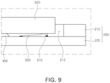
A camera module according to one or more other examples will be described with reference to FIGS. 8 and 9.
A camera module 40 according to the present example may include an optical imaging system 100, a substrate 200, and an image sensor 300. In addition, the camera module 40 may further include an adhesive member 400 and support members 500.
The optical imaging system 100 may include one or more lenses. For example, the optical imaging system 100 according to the present example may include a first lens 110, a second lens 120, and a third lens 130. The optical imaging system 100 may have a focal length. For example, the optical imaging system 100 may have a predetermined back focal length (BF).
The first lens 110 may have positive refractive power. An object-side surface of the first lens 110 may be convex, and an image-side surface thereof may be convex. The first lens 110 may have an aspherical surface. For example, at least one of the object-side surface and the image-side surface of the first lens 110 may be aspherical. The second lens 120 may have positive or negative refractive power. An object-side surface of the second lens 120 may be concave, and an image-side surface thereof may be convex. The second lens 120 may have an aspherical surface. For example, at least one of the object-side surface and the image-side surface of the second lens 120 may be aspherical. The third lens 130 may have positive or negative refractive power. An object-side surface of the third lens 130 may be concave, and an image-side surface thereof may be concave. The third lens 130 may have an aspherical surface. For example, at least one of the object-side surface and the image-side surface of the third lens 130 may be aspherical.
The substrate 200 may include a plurality of members. For example, the substrate 200 may include a first substrate member 210 and a second substrate member 220. A through-hole 212 in which the image sensor 300 may be disposed may be formed in the first substrate member 210. The through-hole 212 may have a shape substantially similar to that of the image sensor 300. For example, the through-hole 212 may have a substantially rectangular cross-sectional shape, similar to the image sensor 300. A cross section of the through-hole 212 may be substantially greater than that of the image sensor 300. A depth of the through-hole 212 may be substantially same as a height of the image sensor 300. However, the depth of the through-hole 212 is not necessarily the same as the height of the image sensor 300. The second substrate member 220 may be disposed beneath the first substrate member 210. The second substrate member 220 may be formed at a size that is substantially the same as that of the first substrate member 210. In addition, the second substrate member 220 may close the through-hole 212 of the first substrate member 210. The second substrate member 220 may be attached to a lower portion of the first substrate member 210 in a process of manufacturing the adhesive member 400 or the substrate 200.
The image sensor 300 may be disposed in the through-hole 212 of the first substrate member 210. The image sensor 300 may convert an optical signal refracted by the optical imaging system 100 into an electrical signal.
The adhesive member 400 may be formed between the substrate 200 and the image sensor 300. For example, the adhesive member 400 may be formed between the second substrate member 220 and the image sensor 300, as illustrated in FIG. 9. The adhesive member 400 formed as described above may be photo-cured or thermally cured to firmly fix the image sensor 300 to the substrate 200.
A portion of the one or more electronic components described above as mounted on the substrate 200 may be mounted on the second substrate member 220.
The support members 500 may be formed on the second substrate member 220. For example, the support members 500 may be formed at intervals along a lower edge of the image sensor 300 or a diagonal length direction of the image sensor 300. The support member 500 may have a bonding wire form. The support members 500 formed as described above may be rapidly and easily formed in a wire bonding process of electrically connecting the second substrate member 220 and the electronic components to each other. In addition, the support member 500 according to the present example may be configured in a bonding wire form having a horizontal portion 510. As an example, the support member 500 having such a form may be formed by pressing a bonding wire having a curved shape with a predetermined force. As another example, a bonding wire having the horizontal portion 510 may be formed by pressing the image sensor 300 in a state in which the image sensor 300 is put on the support member 500. When the support member 500 is formed by the latter method, a distance decrease phenomenon between the optical imaging system 100 and the image sensor 300 due to excessive application of the adhesive member 400 may be solved. The horizontal portion 510 formed as described above may be in line contact with a lower portion of the image sensor 300 to firmly support the image sensor 300.
The support members 500 may support the image sensor 300 at a second height h2 that is significantly low. Here, the second height h2 may be in a range of approximately 50 to 70 μm. In addition, the support members 500 may be formed between the substrate 200 and the image sensor 300 to maintain a constant distance (that is, a back focal length BF) between the optical imaging system 100 and the image sensor 300. For example, the support members 500 may solve a phenomenon in which a distance between the substrate 200 and the image sensor 300 is decreased and the distance between the optical imaging system 100 and the image sensor 300 is increased due to shrinkage-curing of the adhesive member 400.
Therefore, in the camera module 40 according to the present example, quality deterioration phenomenon of the camera module 40 due to the shrinkage-curing of the adhesive member 400 and the excessive application of the adhesive member 400 may be significantly alleviated. In addition, in the camera module 40 according to the example, the image sensor 300 may be disposed in the groove 212 of the first substrate member 210, such that an entire height of the camera module 40 may be decreased.
As set forth above, according to the one or more examples described herein, reliability for optical performance of a camera module may be improved.
While specific examples have been shown and described above, it will be apparent after an understanding of this disclosure that various changes in form and details may be made in these examples without departing from the spirit and scope of the claims and their equivalents. The examples described herein are to be considered in a descriptive sense only, and not for purposes of limitation. Descriptions of features or aspects in each example are to be considered as being applicable to similar features or aspects in other examples. Suitable results may be achieved if the described techniques are performed in a different order, and/or if components in a described system, architecture, device, or circuit are combined in a different manner, and/or replaced or supplemented by other components or their equivalents. Therefore, the scope of this disclosure is defined not by the detailed description, but by the claims and their equivalents, and all variations within the scope of the claims and their equivalents are to be construed as being included in this disclosure.

Claims (18)

What is claimed is:
1. A camera module comprising:
a lens;
an image sensor disposed on a substrate and converting an optical signal refracted by the lens into an electrical signal;
an adhesive member disposed between the substrate and the image sensor to fix the image sensor to the substrate; and
a support member disposed between the substrate and the image sensor configured to maintain a constant distance between the lens and the image sensor even at a time of shrinkage-deformation of the adhesive member,
wherein the support member comprises a bonding wire form.
2. The camera module of claim 1, wherein the support member is disposed along a lower edge of the image sensor.
3. The camera module of claim 1, wherein the adhesive member is partially disposed in a diagonal direction of the image sensor.
4. The camera module of claim 1, wherein the bonding wire comprises a horizontal portion in line contact with a lower portion of the image sensor.
5. A camera module comprising:
a lens;
a substrate comprising a groove;
an image sensor disposed in the groove and converting an optical signal refracted by the lens into an electrical signal;
an adhesive member fixing the image sensor to the groove; and
a support member disposed in the groove configured to maintain a constant distance between the lens and the image sensor even at a time of shrinkage-deformation of the adhesive member,
wherein the support member comprises a bonding wire form.
6. The camera module of claim 5, wherein the adhesive member is disposed between inner surfaces of the groove and side surfaces of the image sensor.
7. The camera module of claim 5, wherein the substrate comprises:
a first substrate member in which a through-hole corresponding to the groove is formed; and
a second substrate member coupled to the first substrate member and closing a lower portion of the through-hole.
8. The camera module of claim 7, wherein the bonding wire comprises a horizontal portion in line contact with a lower portion of the image sensor.
9. A camera module, comprising:
a substrate;
a support member disposed on the substrate;
an image sensor disposed on the support member;
an adhesive member bonded to the substrate and the image sensor, wherein the adhesive member thickness in a direction from the substrate to the image sensor is predetermined by the image sensor disposed against the support member; and
a lens configured to refract light comprising an optical signal converted by the image sensor to an electrical signal,
wherein the support member comprises a plastically deformed portion to align the image sensor and the lens by a predetermined distance.
10. The camera module of claim 9, wherein the support member is spaced apart from the adhesive member.
11. The camera module of claim 9, wherein the image sensor is disposed on a bottom surface of a groove in the substrate, and the adhesive member is further disposed on a side surface of the image sensor between inner surfaces of the groove.
12. The camera module of claim 9, wherein the adhesive member urges the image sensor against the support member.
13. A camera module comprising:
a lens;
a substrate comprising a groove;
an image sensor disposed in the groove and converting an optical signal refracted by the lens into an electrical signal;
an adhesive member fixing the image sensor to the groove; and
a support member disposed in the groove configured to maintain a constant distance between the lens and the image sensor even at a time of shrinkage-deformation of the adhesive member,
wherein the substrate comprises:
a first substrate member in which a through-hole corresponding to the groove is formed; and
a second substrate member coupled to the first substrate member and closing a lower portion of the through-hole.
14. The camera module of claim 13, wherein the adhesive member is disposed between inner surfaces of the groove and side surfaces of the image sensor.
15. The camera module of claim 13, wherein the support member is disposed along a lower edge of the image sensor.
16. The camera module of claim 13, wherein the adhesive member is partially disposed in a diagonal direction of the image sensor.
17. The camera module of claim 13, wherein the support member is spaced apart from the adhesive member.
18. The camera module of claim 13, wherein the adhesive member urges the image sensor against the support member.
US16/750,344 2019-05-20 2020-01-23 Camera module Active 2040-04-10 US11252311B2 (en)

Priority Applications (1)

Application Number Priority Date Filing Date Title
US17/567,646 US11706510B2 (en) 2019-05-20 2022-01-03 Camera module

Applications Claiming Priority (2)

Application Number Priority Date Filing Date Title
KR10-2019-0058814 2019-05-20
KR1020190058814A KR102185047B1 (en) 2019-05-20 2019-05-20 Camera Module

Related Child Applications (1)

Application Number Title Priority Date Filing Date
US17/567,646 Continuation US11706510B2 (en) 2019-05-20 2022-01-03 Camera module

Publications (2)

Publication Number Publication Date
US20200374426A1 US20200374426A1 (en) 2020-11-26
US11252311B2 true US11252311B2 (en) 2022-02-15

Family

ID=73162596

Family Applications (2)

Application Number Title Priority Date Filing Date
US16/750,344 Active 2040-04-10 US11252311B2 (en) 2019-05-20 2020-01-23 Camera module
US17/567,646 Active US11706510B2 (en) 2019-05-20 2022-01-03 Camera module

Family Applications After (1)

Application Number Title Priority Date Filing Date
US17/567,646 Active US11706510B2 (en) 2019-05-20 2022-01-03 Camera module

Country Status (3)

Country Link
US (2) US11252311B2 (en)
KR (1) KR102185047B1 (en)
CN (2) CN211959328U (en)

Cited By (1)

* Cited by examiner, † Cited by third party
Publication number Priority date Publication date Assignee Title
US20220132005A1 (en) * 2019-05-20 2022-04-28 Samsung Electro-Mechanics Co., Ltd. Camera module

Families Citing this family (1)

* Cited by examiner, † Cited by third party
Publication number Priority date Publication date Assignee Title
CN114630018A (en) * 2020-12-14 2022-06-14 晋城三赢精密电子有限公司 Lens module and electronic device

Citations (19)

* Cited by examiner, † Cited by third party
Publication number Priority date Publication date Assignee Title
US20060082658A1 (en) 2004-10-18 2006-04-20 Samsung Electronics Co.; Ltd Device for image stabilization of camera module
CN101064779A (en) 2006-04-27 2007-10-31 中兴通讯股份有限公司 Method for realizing minisize camera automatic focusing and minisize camera thereof
KR20090004352U (en) 2007-11-05 2009-05-11 엘지이노텍 주식회사 Reinforce structure of image sensor for camera module
KR20110024854A (en) 2009-09-03 2011-03-09 삼성전기주식회사 Camera module
US20120211852A1 (en) 2011-02-18 2012-08-23 Sony Corporation Solid-state imaging apparatus
US20130271649A1 (en) 2012-04-17 2013-10-17 Stmicroelectronics (Research & Development) Limited Camera module, method of assembly and imaging device
US20140138551A1 (en) 2012-11-21 2014-05-22 Zakrytoe Akcionernoe Obshchestvo "Impul's" X-ray Imaging Detector, Method for Manufacturing a Photosensitive Element and an X-ray Imaging Detector
US20140374870A1 (en) * 2013-06-19 2014-12-25 Samsung Electro-Mechanics Co., Ltd. Image sensor module and method of manufacturing the same
CN104333679A (en) 2013-07-22 2015-02-04 鸿富锦精密工业(深圳)有限公司 Camera module
KR20150025831A (en) 2013-08-30 2015-03-11 삼성전자주식회사 Image sensor chip package and image sensor module having the same
CN105405771A (en) 2014-09-11 2016-03-16 旭景科技股份有限公司 Method of mounting chip on printed circuit board
US20160116701A1 (en) * 2013-07-30 2016-04-28 Kyocera Corporation Substrate for mounting imaging element, and imaging device
US20160141235A1 (en) * 2014-11-18 2016-05-19 Sunasic Technologies, Inc. Printed circuit board assembly with image sensor mounted thereon
KR20170037459A (en) 2015-09-25 2017-04-04 삼성전기주식회사 Image sensor module and method of manufacturing thereof
US20170154913A1 (en) * 2015-12-01 2017-06-01 Hyunsu Jun Semiconductor package
CN106803870A (en) 2015-11-26 2017-06-06 三星电机株式会社 Camera model
TWI639880B (en) 2017-11-10 2018-11-01 群光電子股份有限公司 Lens structure and method for correcting thermal drift
CN109618080A (en) 2018-12-11 2019-04-12 维沃移动通信(杭州)有限公司 Camera module and mobile terminal
US20190202136A1 (en) * 2017-12-29 2019-07-04 Intel Corporation Component coupling via plurality of adhesive elements

Family Cites Families (4)

* Cited by examiner, † Cited by third party
Publication number Priority date Publication date Assignee Title
KR20090004352A (en) 2007-11-26 2009-01-12 엘지전자 주식회사 Method for performing cell search procedure in wireless communication system
US9760754B2 (en) * 2015-07-06 2017-09-12 Sunasic Technologies Inc. Printed circuit board assembly forming enhanced fingerprint module
KR102185047B1 (en) * 2019-05-20 2020-12-01 삼성전기주식회사 Camera Module
KR20210021172A (en) * 2019-08-14 2021-02-25 삼성전자주식회사 Semiconductor package comprising an image sensor chip

Patent Citations (22)

* Cited by examiner, † Cited by third party
Publication number Priority date Publication date Assignee Title
US20060082658A1 (en) 2004-10-18 2006-04-20 Samsung Electronics Co.; Ltd Device for image stabilization of camera module
CN1763625A (en) 2004-10-18 2006-04-26 三星电子株式会社 The device for image stabilization of camera module
CN101064779A (en) 2006-04-27 2007-10-31 中兴通讯股份有限公司 Method for realizing minisize camera automatic focusing and minisize camera thereof
KR20090004352U (en) 2007-11-05 2009-05-11 엘지이노텍 주식회사 Reinforce structure of image sensor for camera module
KR20110024854A (en) 2009-09-03 2011-03-09 삼성전기주식회사 Camera module
US20120211852A1 (en) 2011-02-18 2012-08-23 Sony Corporation Solid-state imaging apparatus
US20130271649A1 (en) 2012-04-17 2013-10-17 Stmicroelectronics (Research & Development) Limited Camera module, method of assembly and imaging device
US20140138551A1 (en) 2012-11-21 2014-05-22 Zakrytoe Akcionernoe Obshchestvo "Impul's" X-ray Imaging Detector, Method for Manufacturing a Photosensitive Element and an X-ray Imaging Detector
CN103839954A (en) 2012-11-21 2014-06-04 伊姆普斯封闭式股份有限公司 X-ray imaging detector, method for manufacturing a photosensitive element and an x-ray imaging detector
KR20140147410A (en) 2013-06-19 2014-12-30 삼성전기주식회사 Image Sensor Module and Method of Manufacturing for the Same
US20140374870A1 (en) * 2013-06-19 2014-12-25 Samsung Electro-Mechanics Co., Ltd. Image sensor module and method of manufacturing the same
CN104333679A (en) 2013-07-22 2015-02-04 鸿富锦精密工业(深圳)有限公司 Camera module
US20160116701A1 (en) * 2013-07-30 2016-04-28 Kyocera Corporation Substrate for mounting imaging element, and imaging device
KR20150025831A (en) 2013-08-30 2015-03-11 삼성전자주식회사 Image sensor chip package and image sensor module having the same
CN105405771A (en) 2014-09-11 2016-03-16 旭景科技股份有限公司 Method of mounting chip on printed circuit board
US20160141235A1 (en) * 2014-11-18 2016-05-19 Sunasic Technologies, Inc. Printed circuit board assembly with image sensor mounted thereon
KR20170037459A (en) 2015-09-25 2017-04-04 삼성전기주식회사 Image sensor module and method of manufacturing thereof
CN106803870A (en) 2015-11-26 2017-06-06 三星电机株式会社 Camera model
US20170154913A1 (en) * 2015-12-01 2017-06-01 Hyunsu Jun Semiconductor package
TWI639880B (en) 2017-11-10 2018-11-01 群光電子股份有限公司 Lens structure and method for correcting thermal drift
US20190202136A1 (en) * 2017-12-29 2019-07-04 Intel Corporation Component coupling via plurality of adhesive elements
CN109618080A (en) 2018-12-11 2019-04-12 维沃移动通信(杭州)有限公司 Camera module and mobile terminal

Non-Patent Citations (2)

* Cited by examiner, † Cited by third party
Title
Chinese Office Action dated Jun. 3, 2021 in Counterpart Chinese Patent Application No. 202010316434.8 (7 pages in English and 8 pages in Chinese).
Korean Office Action dated Apr. 6, 2020 in counterpart Korean Patent Application No. 10-2019-0058814 (8 pages in English and 5 pages in Korean).

Cited By (2)

* Cited by examiner, † Cited by third party
Publication number Priority date Publication date Assignee Title
US20220132005A1 (en) * 2019-05-20 2022-04-28 Samsung Electro-Mechanics Co., Ltd. Camera module
US11706510B2 (en) * 2019-05-20 2023-07-18 Samsung Electro-Mechanics Co., Ltd. Camera module

Also Published As

Publication number Publication date
CN111970417B (en) 2022-06-03
US20220132005A1 (en) 2022-04-28
KR20200133502A (en) 2020-11-30
CN111970417A (en) 2020-11-20
CN211959328U (en) 2020-11-17
KR102185047B1 (en) 2020-12-01
US11706510B2 (en) 2023-07-18
US20200374426A1 (en) 2020-11-26

Similar Documents

Publication Publication Date Title
US11885942B2 (en) Optical imaging system
JP6513779B2 (en) Imaging lens and imaging apparatus
US11706510B2 (en) Camera module
US20180180856A1 (en) Optical imaging system
CN111034169B (en) Camera module and assembling method thereof
TWI771472B (en) Optical image capturing module、system and manufacturing method thereof
US11609361B2 (en) Lens assembly and portable electronic device
US11269161B2 (en) Optical imaging system having six lenses of +−+−+− refractive powers
US20160154211A1 (en) Optical system
US11927730B2 (en) Optical imaging system
TWI768103B (en) Optical image capturing module、system and manufacturing method thereof
TWI768105B (en) Optical image capturing module, system and manufacturing method thereof
TWM575127U (en) Optical imaging module and imaging system thereof
TW202010147A (en) Optical image capturing module、system and manufacturing method thereof
US20090122180A1 (en) Imaging system with relaxed assembly tolerances and associated methods
US11122191B2 (en) Camera module and portable terminal
CN112987453B (en) camera module
US9366848B2 (en) Wafer-level lens systems and methods for manufacturing the same
CN210294780U (en) Optical imaging module
KR102385410B1 (en) Camera Module
JP2000098223A (en) Lens and optical module
JP2010050725A (en) Imaging unit, method for manufacturing imaging unit, and imaging apparatus

Legal Events

Date Code Title Description
AS Assignment

Owner name: SAMSUNG ELECTRO-MECHANICS CO., LTD., KOREA, REPUBLIC OF

Free format text: ASSIGNMENT OF ASSIGNORS INTEREST;ASSIGNORS:GU, WON SEO;SIN, SOO GIL;KIM, SANG JIN;REEL/FRAME:051598/0181

Effective date: 20191223

FEPP Fee payment procedure

Free format text: ENTITY STATUS SET TO UNDISCOUNTED (ORIGINAL EVENT CODE: BIG.); ENTITY STATUS OF PATENT OWNER: LARGE ENTITY

STPP Information on status: patent application and granting procedure in general

Free format text: DOCKETED NEW CASE - READY FOR EXAMINATION

STPP Information on status: patent application and granting procedure in general

Free format text: NON FINAL ACTION MAILED

STPP Information on status: patent application and granting procedure in general

Free format text: RESPONSE TO NON-FINAL OFFICE ACTION ENTERED AND FORWARDED TO EXAMINER

STPP Information on status: patent application and granting procedure in general

Free format text: NOTICE OF ALLOWANCE MAILED -- APPLICATION RECEIVED IN OFFICE OF PUBLICATIONS

STPP Information on status: patent application and granting procedure in general

Free format text: NOTICE OF ALLOWANCE MAILED -- APPLICATION RECEIVED IN OFFICE OF PUBLICATIONS

STPP Information on status: patent application and granting procedure in general

Free format text: PUBLICATIONS -- ISSUE FEE PAYMENT VERIFIED

STCF Information on status: patent grant

Free format text: PATENTED CASE