US11233967B2 - AD conversion circuit, imaging device, and endoscope system - Google Patents
AD conversion circuit, imaging device, and endoscope system Download PDFInfo
- Publication number
- US11233967B2 US11233967B2 US16/940,748 US202016940748A US11233967B2 US 11233967 B2 US11233967 B2 US 11233967B2 US 202016940748 A US202016940748 A US 202016940748A US 11233967 B2 US11233967 B2 US 11233967B2
- Authority
- US
- United States
- Prior art keywords
- voltage
- terminal
- signal
- switch
- input terminal
- Prior art date
- Legal status (The legal status is an assumption and is not a legal conclusion. Google has not performed a legal analysis and makes no representation as to the accuracy of the status listed.)
- Active
Links
Images


Classifications
-
- H04N5/378—
-
- H—ELECTRICITY
- H03—ELECTRONIC CIRCUITRY
- H03M—CODING; DECODING; CODE CONVERSION IN GENERAL
- H03M1/00—Analogue/digital conversion; Digital/analogue conversion
- H03M1/12—Analogue/digital converters
- H03M1/50—Analogue/digital converters with intermediate conversion to time interval
- H03M1/56—Input signal compared with linear ramp
-
- G—PHYSICS
- G02—OPTICS
- G02B—OPTICAL ELEMENTS, SYSTEMS OR APPARATUS
- G02B23/00—Telescopes, e.g. binoculars; Periscopes; Instruments for viewing the inside of hollow bodies; Viewfinders; Optical aiming or sighting devices
- G02B23/24—Instruments or systems for viewing the inside of hollow bodies, e.g. fibrescopes
- G02B23/2407—Optical details
- G02B23/2461—Illumination
- G02B23/2469—Illumination using optical fibres
-
- H—ELECTRICITY
- H03—ELECTRONIC CIRCUITRY
- H03M—CODING; DECODING; CODE CONVERSION IN GENERAL
- H03M1/00—Analogue/digital conversion; Digital/analogue conversion
- H03M1/12—Analogue/digital converters
- H03M1/1205—Multiplexed conversion systems
- H03M1/123—Simultaneous, i.e. using one converter per channel but with common control or reference circuits for multiple converters
-
- H—ELECTRICITY
- H03—ELECTRONIC CIRCUITRY
- H03M—CODING; DECODING; CODE CONVERSION IN GENERAL
- H03M1/00—Analogue/digital conversion; Digital/analogue conversion
- H03M1/12—Analogue/digital converters
- H03M1/124—Sampling or signal conditioning arrangements specially adapted for A/D converters
-
- H—ELECTRICITY
- H03—ELECTRONIC CIRCUITRY
- H03M—CODING; DECODING; CODE CONVERSION IN GENERAL
- H03M1/00—Analogue/digital conversion; Digital/analogue conversion
- H03M1/12—Analogue/digital converters
- H03M1/34—Analogue value compared with reference values
-
- H—ELECTRICITY
- H04—ELECTRIC COMMUNICATION TECHNIQUE
- H04N—PICTORIAL COMMUNICATION, e.g. TELEVISION
- H04N25/00—Circuitry of solid-state image sensors [SSIS]; Control thereof
- H04N25/70—SSIS architectures; Circuits associated therewith
- H04N25/76—Addressed sensors, e.g. MOS or CMOS sensors
- H04N25/77—Pixel circuitry, e.g. memories, A/D converters, pixel amplifiers, shared circuits or shared components
- H04N25/778—Pixel circuitry, e.g. memories, A/D converters, pixel amplifiers, shared circuits or shared components comprising amplifiers shared between a plurality of pixels, i.e. at least one part of the amplifier must be on the sensor array itself
-
- H—ELECTRICITY
- H04—ELECTRIC COMMUNICATION TECHNIQUE
- H04N—PICTORIAL COMMUNICATION, e.g. TELEVISION
- H04N25/00—Circuitry of solid-state image sensors [SSIS]; Control thereof
- H04N25/70—SSIS architectures; Circuits associated therewith
- H04N25/76—Addressed sensors, e.g. MOS or CMOS sensors
- H04N25/78—Readout circuits for addressed sensors, e.g. output amplifiers or A/D converters
-
- H04N5/37455—
-
- H04N5/37457—
-
- G—PHYSICS
- G02—OPTICS
- G02B—OPTICAL ELEMENTS, SYSTEMS OR APPARATUS
- G02B23/00—Telescopes, e.g. binoculars; Periscopes; Instruments for viewing the inside of hollow bodies; Viewfinders; Optical aiming or sighting devices
- G02B23/24—Instruments or systems for viewing the inside of hollow bodies, e.g. fibrescopes
- G02B23/2476—Non-optical details, e.g. housings, mountings, supports
- G02B23/2484—Arrangements in relation to a camera or imaging device
Definitions
- the present invention relates to an AD conversion circuit, an imaging device, and an endoscope system.
- Physical quantity detection semiconductor devices having sensors sensitive to externally input electromagnetic waves (light, radiation, etc.) are used in various fields.
- a physical quantity is converted into an electrical signal by a sensor.
- a sensor in an imaging device is a pixel.
- electrical signals of a reference level and a signal level are read from the sensor.
- the reference level in the imaging device is a reset level.
- a single-slope-type ADC As an AD conversion circuit (ADC) of an imaging device, a single-slope-type ADC (SS-type ADC) is generally used.
- the SS-type ADC compares an analog signal given to one input terminal of a comparator with a reference signal given to the other input terminal of the comparator.
- the reference signal decreases or increases as time passes.
- the SS-type ADC performs AD conversion by measuring the length of time until the voltage of the analog signal and the voltage of the reference signal match each other.
- the comparator After voltages of two input terminals of a differential amplifier included in the comparator are reset, the comparator starts comparison. Through the resetting, the voltages of the two input terminals become almost the same. There is a case in which some variation remains in the voltages of the two input terminals after the resetting. For this reason, there is a case in which the output of the comparator is not inverted or a malfunction occurs in which the output of the comparator is inverted immediately after the reference signal is input.
- an AD conversion circuit includes a comparator, a reset circuit, a measurement circuit, and a first signal generation circuit.
- the comparator that includes a first input terminal to which a first analog signal and a second analog signal are input and a second input terminal to which a reference signal having a voltage that is configured to gradually change is input.
- the comparator is configured to compare a first voltage of the first input terminal with a second voltage of the second input terminal.
- the comparator is configured to output a signal that represents a result of comparing the first voltage with the second voltage.
- the comparator is configured to complete comparing the first voltage with the second voltage when an amount of the first voltage and an amount of the second voltage satisfy a predetermined condition.
- the reset circuit is configured to reset a voltage of the first input terminal of the comparator and a voltage of the second input terminal of the comparator when the second analog signal is input to the first input terminal of the comparator.
- the measurement circuit is configured to measure a length of time from a timing at which the comparator starts comparing the first voltage with the second voltage to a timing at which the comparator completes comparing the first voltage with the second voltage.
- the first signal generation circuit is configured to generate the second analog signal having a third voltage higher or lower than a voltage of the first analog signal. The first analog signal is input to the first input terminal of the comparator after the voltage of the first input terminal of the comparator and the voltage of the second input terminal of the comparator are reset.
- the comparator is configured to start comparing the first voltage with the second voltage after the first analog signal is input to the first input terminal of the comparator.
- a voltage of the reference signal gradually decreases when the third voltage of the second analog signal is higher than the voltage of the first analog signal.
- the voltage of the reference signal gradually increases when the third voltage of the second analog signal is lower than the voltage of the first analog signal.
- an imaging device includes the AD conversion circuit, a plurality of pixels, a column circuit, and a second signal generation circuit.
- the plurality of pixels that are disposed in a matrix shape and are configured to output a first pixel signal having a signal level and a second pixel signal having a reset level.
- the column circuit is disposed so as to correspond to one or more columns in an array of the plurality of pixels and is configured to generate a difference signal in accordance with a difference between the reset level and the signal level.
- the second signal generation circuit is configured to generate the first analog signal on the basis of the difference signal and the second analog signal.
- the second signal generation circuit may include a differential amplifier, a first resistance element, and a second resistance element.
- the differential amplifier may include a first input terminal, a second input terminal, and an output terminal.
- Each of the first resistance element and the second resistance element may include a first terminal and a second terminal.
- the difference signal may be input to the first input terminal of the differential amplifier.
- the first terminals of the first resistance element and the second resistance element may be connected to the second input terminal of the differential amplifier.
- the second analog signal may be input to the second terminal of the first resistance element.
- the second terminal of the second resistance element may be connected to the output terminal of the differential amplifier.
- the column circuit may include a first capacitance element configured to hold the difference signal.
- the second signal generation circuit may include a differential amplifier and a second capacitance element.
- the differential amplifier may include a first input terminal, a second input terminal, and an output terminal.
- the second capacitance element may include a first terminal and a second terminal.
- the difference signal may be input to the second input terminal of the differential amplifier.
- the first terminal of the second capacitance element may be connected to the second input terminal of the differential amplifier.
- the second terminal of the second capacitance element may be connected to the output terminal of the differential amplifier.
- a signal that is based on the second analog signal may be input to the first input terminal of the differential amplifier.
- an imaging device includes the AD conversion circuit, a plurality of pixels, a column circuit, and a second signal generation circuit.
- the plurality of pixels that are disposed in a matrix shape and are configured to output a first pixel signal having a signal level and a second pixel signal having a reset level.
- the first pixel signal and the second pixel signal are sequentially input to the first input terminal of the comparator as the first analog signal.
- an endoscope system includes the imaging device.
- FIG. 1 is a diagram showing a configuration of an imaging device according to a first embodiment of the present invention.
- FIG. 2 is a block diagram showing a configuration of a first substrate according to the first embodiment of the present invention.
- FIG. 3 is a circuit diagram showing a configuration of a pixel according to the first embodiment of the present invention.
- FIG. 4 is a circuit diagram showing a configuration of a column circuit according to the first embodiment of the present invention.
- FIG. 5 is a circuit diagram showing a configuration of a first reference signal generation circuit and an output unit according to the first embodiment of the present invention.
- FIG. 6 is a circuit diagram showing a configuration of a second substrate according to the first embodiment of the present invention.
- FIG. 7 is a circuit diagram showing a configuration of a comparator according to the first embodiment of the present invention.
- FIG. 8 is a timing chart showing an operation of the imaging device according to the first embodiment of the present invention.
- FIG. 9 is a timing chart showing an operation of an imaging device according to a first modified example of the first embodiment of the present invention.
- FIG. 10 is a circuit diagram showing a configuration of a second substrate according to a second modified example of the first embodiment of the present invention.
- FIG. 11 is a timing chart showing an operation of an imaging device according to the second modified example of the first embodiment of the present invention.
- FIG. 12 is a circuit diagram showing a configuration of a second substrate according to a third modified example of the first embodiment of the present invention.
- FIG. 13 is a timing chart showing an operation of an imaging device according to the third modified example of the first embodiment of the present invention.
- FIG. 14 is a circuit diagram showing a configuration of a second substrate according to a fourth modified example of the first embodiment of the present invention.
- FIG. 15 is a block diagram showing a configuration of a first substrate according to a second embodiment of the present invention.
- FIG. 16 is a circuit diagram showing a configuration of a column circuit according to the second embodiment of the present invention.
- FIG. 17 is a circuit diagram showing a configuration of a first reference signal generation circuit and an output unit according to the second embodiment of the present invention.
- FIG. 18 is a block diagram showing a configuration of a first substrate according to a third embodiment of the present invention.
- FIG. 19 is a circuit diagram showing a configuration of a first reference signal generation circuit and an output unit according to the third embodiment of the present invention.
- FIG. 20 is a diagram showing a configuration of an imaging device according to a fourth embodiment of the present invention.
- FIG. 21 is a block diagram showing a configuration of an endoscope system according to a fifth embodiment of the present invention.
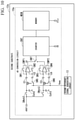
- FIG. 1 shows a configuration of an imaging device 1 according to a first embodiment of the present invention.
- the imaging device 1 includes a first substrate 11 and a second substrate 12 stacked on the first substrate 11 .
- the second substrate 12 is stacked in a stacking direction D 1 with respect to the first substrate 11 .
- the stacking direction D 1 is a direction perpendicular to a main surface of the first substrate 11 or the second substrate 12 .
- the first substrate 11 and the second substrate 12 are connected to each other through Cu—Cu bonding or the like.
- FIG. 2 shows a configuration of the first substrate 11 .
- the first substrate 11 includes an imaging unit 2 , a vertical selection unit 4 , a column circuit unit 5 , a horizontal selection unit 6 , an output unit 7 , and a first reference signal generation circuit 9 (first signal generation circuit).
- the imaging unit 2 includes a plurality of pixels 3 disposed in a matrix shape.
- the plurality of pixels 3 constitute an array having m rows and n columns.
- the number m and the number n are integers of two or more.
- the number of rows and the number of columns may not be the same. In FIG. 2 , an example in which the number of rows is two and the number of columns is three is shown. This is only an example and the present invention is not limited to this.
- the pixel 3 outputs a first pixel signal having a signal level and a second pixel signal having a reset level.
- the vertical selection unit 4 selects the pixel 3 disposed in the row direction in the array of the plurality of pixels 3 .
- the vertical selection unit 4 controls an operation of the selected pixel 3 .
- the vertical selection unit 4 outputs control signals for controlling the plurality of pixels 3 for each row in the array of the plurality of pixels 3 .
- the control signals output from the vertical selection unit 4 include a transfer pulse ⁇ Tx_i, a reset pulse ⁇ Rst_i, and a selection pulse ⁇ Sel_i.
- the number i is one or two.
- the transfer pulse ⁇ Tx_ 1 , the reset pulse ⁇ Rst_ 1 , and the selection pulse ⁇ Sel_ 1 are output to the pixels 3 of the first row.
- the transfer pulse ⁇ Tx_ 2 , the reset pulse ⁇ Rst_ 2 , and the selection pulse ⁇ Sel_ 2 are output to the pixels 3 of the second row.
- the column circuit unit 5 includes a plurality of column circuits 8 .
- the column circuit 8 is disposed for each column in the array of the plurality of pixels 3 .
- the column circuit 8 is connected to a vertical signal line 20 extending in the vertical direction, i.e., the column direction.
- the vertical signal line 20 is disposed for each column in the array of the plurality of pixels 3 .
- the vertical signal line 20 is connected to the pixels 3 of each column.
- the column circuit 8 is electrically connected to the pixels 3 through the vertical signal line 20 .
- the column circuit 8 generates a difference signal in accordance with the difference between the signal level and the reset level output from the pixel 3 .
- the column circuit 8 is connected to a horizontal signal line 21 extending in the horizontal direction, i.e., the row direction.
- a selection pulse HSR[k] is output from the horizontal selection unit 6 to the column circuit 8 corresponding to a column k.
- the number k is any one of one, two, and three.
- the column circuit 8 selected on the basis of the selection pulse HSR[k] outputs the difference signal to the horizontal signal line 21 .
- One column circuit 8 may be disposed for a plurality of columns in the array of the plurality of pixels 3 and one column circuit 8 may be used in the plurality of columns in a time-division manner. Therefore, the column circuit 8 has only to be disposed so as to correspond to one or more columns in the array of the plurality of pixels 3 .
- the horizontal signal line 21 is connected to the output unit 7 .
- a first current source I 1 is connected to the horizontal signal line 21 .
- the horizontal selection unit 6 sequentially selects the column circuits 8 by using the selection pulses HSR[ 1 ] to HSR[ 3 ].
- the difference signal output from the column circuit 8 selected by the horizontal selection unit 6 is transferred to the output unit 7 .
- the output unit 7 outputs the difference signal output from the column circuit 8 and a first reference signal output from the first reference signal generation circuit 9 to the second substrate 12 .
- the first reference signal generation circuit 9 generates the first reference signal and outputs the generated first reference signal to the output unit 7 .
- the first reference signal generation circuit 9 is included in an analog-to-digital conversion circuit (AD conversion circuit) 10 .
- FIG. 3 shows a configuration of the pixel 3 .
- the pixel 3 includes a photoelectric conversion unit PD, a transfer transistor Tx, a charge storage portion FD, a reset transistor Rst, an amplification transistor Drv, and a selection transistor Sel.
- Each transistor shown in FIG. 3 is an NMOS transistor.
- Each transistor shown in FIG. 3 includes a gate terminal, a source terminal, and a drain terminal.
- the photoelectric conversion unit PD is a photodiode.
- the photoelectric conversion unit PD includes a first terminal and a second terminal.
- the first terminal of the photoelectric conversion unit PD is connected to the ground.
- the second terminal of the photoelectric conversion unit PD is connected to the transfer transistor Tx.
- the source terminal of the transfer transistor Tx is connected to the second terminal of the photoelectric conversion unit PD.
- the drain terminal of the transfer transistor Tx is connected to the charge storage portion FD.
- the gate terminal of the transfer transistor Tx is connected to a control signal line 32 .
- the control signal line 32 extends from the vertical selection unit 4 in the row direction in the array of the plurality of pixels 3 .
- the control signal line 32 transfers the transfer pulse ⁇ Tx_i.
- the drain terminal of the reset transistor Rst is connected to a power source line 30 .
- the power source line 30 is connected to a power source that outputs a power source voltage VDD.
- the source terminal of the reset transistor Rst is connected to the charge storage portion FD.
- the gate terminal of the reset transistor Rst is connected to a control signal line 31 .
- the control signal line 31 extends from the vertical selection unit 4 in the row direction in the array of the plurality of pixels 3 .
- the control signal line 31 transfers the reset pulse ⁇ Rst_i.
- the drain terminal of the amplification transistor Drv is connected to the power source line 30 .
- the source terminal of the amplification transistor Drv is connected to the selection transistor Sel.
- the gate terminal of the amplification transistor Drv is connected to the charge storage portion FD.
- the drain terminal of the selection transistor Sel is connected to the source terminal of the amplification transistor Drv.
- the source terminal of the selection transistor Sel is connected to the vertical signal line 20 .
- the gate terminal of the selection transistor Sel is connected to a control signal line 33 .
- the control signal line 33 extends from the vertical selection unit 4 in the row direction in the array of the plurality of pixels 3 .
- the control signal line 33 transfers the selection pulse ⁇ Sel_i.
- the transfer transistor Tx is controlled on the basis of the transfer pulse ⁇ Tx_i output from the vertical selection unit 4 .
- the transfer transistor Tx of the pixel 3 of the first row is controlled on the basis of the transfer pulse ⁇ Tx_ 1 and the transfer transistor Tx of the pixel 3 of the second row is controlled on the basis of the transfer pulse ⁇ Tx_ 2 .
- the reset transistor Rst is controlled on the basis of the reset pulse ⁇ Rst_i output from the vertical selection unit 4 .
- the reset transistor Rst of the pixel 3 of the first row is controlled on the basis of the reset pulse ⁇ Rst_ 1 and the reset transistor Rst of the pixel 3 of the second row is controlled on the basis of the reset pulse ⁇ Rst_ 2 .
- the selection transistor Sel is controlled on the basis of the selection pulse ⁇ Sel_i output from the vertical selection unit 4 .
- the selection transistor Sel of the pixel 3 of the first row is controlled on the basis of the selection pulse ⁇ Sel_ 1 and the selection transistor Sel of the pixel 3 of the second row is controlled on the basis of the selection pulse ⁇ Sel_ 2 .
- the photoelectric conversion unit PD generates signal charge in accordance with the amount of incident light.
- the transfer transistor Tx transfers the signal charge generated by the photoelectric conversion unit PD to the charge storage portion PD.
- the charge storage portion FD is a floating diffusion.
- the charge storage portion FD stores the signal charge transferred by the transfer transistor Tx.
- the reset transistor Rst resets the charge storage portion FD to a predetermined voltage.
- the amplification transistor Drv generates a pixel signal by amplifying a signal in accordance with a voltage of the charge storage portion FD.
- the selection transistor Sel outputs the pixel signal to the vertical signal line 20 .
- the vertical signal line 20 is disposed for each column in the array of the plurality of pixels 3 .
- the first pixel signal having the signal level and the second pixel signal having the reset level are output from the pixel 3 .
- the signal level has a voltage that is based on the signal charge generated by the photoelectric conversion unit PD.
- the reset level has a voltage that is based on the voltage of the charge storage portion FD when the voltage of the charge storage portion FD is reset.
- FIG. 4 shows a configuration of the column circuit 8 .
- the column circuit 8 includes a transistor M 1 , a capacitance element Cclp 1 , a clamp switch SWclp 1 , an amplification transistor M 2 , and a column selection transistor M 3 .
- Each transistor shown in FIG. 4 is an NMOS transistor.
- Each transistor shown in FIG. 4 includes a gate terminal, a source terminal, and a drain terminal.
- the drain terminal of the transistor M 1 is connected to the vertical signal line 20 .
- the source terminal of the transistor M 1 is connected to the ground.
- the gate terminal of the transistor M 1 is connected to the power source line 34 .
- the power source line 34 is connected to a power source that outputs a predetermined voltage LMB.
- the capacitance element Cclp 1 includes a first terminal and a second terminal.
- the first terminal of the capacitance element Cclp 1 is connected to the vertical signal line 20 .
- the second terminal of the capacitance element Cclp 1 is connected to the clamp switch SWclp 1 and the amplification transistor M 2 .
- the clamp switch SWclp 1 includes a first terminal and a second terminal.
- the first terminal of the clamp switch SWclp 1 is connected to the second terminal of the capacitance element Cclp 1 .
- a clamp voltage Vclp is input to the second terminal of the clamp switch SWclp 1 .
- the power source voltage VDD is input to the drain terminal of the amplification transistor M 2 .
- the source terminal of the amplification transistor M 2 is connected to the column selection transistor M 3 .
- the gate terminal of the amplification transistor M 2 is connected to the second terminal of the capacitance element Cclp 1 .
- the drain terminal of the column selection transistor M 3 is connected to the source terminal of the amplification transistor M 2 .
- the source terminal of the column selection transistor M 3 is connected to the horizontal signal line 21 .
- the gate terminal of the column selection transistor M 3 is connected to the horizontal selection unit 6 .
- An operation of the clamp switch SWclp 1 is controlled on the basis of a clamp pulse ⁇ CLP.
- An operation of the column selection transistor M 3 is controlled on the basis of a selection pulse HSR[k] output from the horizontal selection unit 6 .
- the number k is any one of one, two, and three.
- the transistor M 1 functions as a current source.
- the state of the clamp switch SWclp 1 becomes any one of an ON state and an OFF state.
- the capacitance element Cclp 1 is clamped to the clamp voltage Vclp.
- the capacitance element Cclp 1 holds the pixel signal in accordance with the difference between the reset level and the signal level output from the pixel 3 to the vertical signal line 20 .
- the capacitance element Cclp 1 is a clamp capacitor.
- the amplification transistor M 2 generates the difference signal in accordance with the difference between the reset level and the signal level by amplifying the pixel signal held in the capacitance element Cclp 1 .
- the column selection transistor M 3 outputs the difference signal generated by the amplification transistor M 2 to the horizontal signal line 21 .
- the column selection transistor M 3 of the first column is controlled on the basis of a selection pulse HSR[ 1 ].
- the column selection transistor M 3 of the second column is controlled on the basis of a selection pulse HSR[ 2 ].
- the column selection transistor M 3 of the third column is controlled on the basis of a selection pulse HSR[ 3 ].
- FIG. 5 shows a configuration of the first reference signal generation circuit 9 and the output unit 7 .
- the first reference signal generation circuit 9 includes a sample switch SWsh 1 , a capacitance element Csh 1 , a buffer Bf 1 , a capacitance element Cclp 2 , a clamp switch SWclp 2 , an amplification transistor M 2 a , a selection transistor M 3 a , and a second current source I 2 .
- the sample switch SWsh 1 includes a first terminal and a second terminal. A voltage Vrst is input to the first terminal of the sample switch SWsh 1 . The second terminal of the sample switch SWsh 1 is connected to the capacitance element Csh 1 .
- the capacitance element Csh 1 includes a first terminal and a second terminal.
- the first terminal of the capacitance element Csh 1 is connected to the second terminal of the sample switch SWsh 1 .
- the second terminal of the capacitance element Csh 1 is connected to the ground.
- the buffer Bf 1 includes a first terminal and a second terminal.
- the first terminal of the buffer Bf 1 is connected to the second terminal of the sample switch SWsh 1 and the first terminal of the capacitance element Csh 1 .
- the second terminal of the buffer Bf 1 is connected to the capacitance element Cclp 2 .
- the capacitance element Cclp 2 includes a first terminal and a second terminal.
- the first terminal of the capacitance element Cclp 2 is connected to the second terminal of the buffer Bf 1 .
- the second terminal of the capacitance element Cclp 2 is connected to the clamp switch SWclp 2 and the amplification transistor M 2 a.
- the clamp switch SWclp 2 includes a first terminal and a second terminal.
- the first terminal of the clamp switch SWclp 2 is connected to the second terminal of the capacitance element Cclp 2 .
- the clamp voltage Vclp is input to the second terminal of the clamp switch SWclp 2 .
- the amplification transistor M 2 a and the selection transistor M 3 a are NMOS transistors. Each of the amplification transistor M 2 a and the selection transistor M 3 a includes a gate terminal, a source terminal, and a drain terminal. The power source voltage VDD is input to the drain terminal of the amplification transistor M 2 a . The source terminal of the amplification transistor M 2 a is connected to the selection transistor M 3 a and the output unit 7 . The gate terminal of the amplification transistor M 2 a is connected to the second terminal of the capacitance element Cclp 2 .
- the drain terminal of the selection transistor M 3 a is connected to the source terminal of the amplification transistor M 2 a .
- the source terminal of the selection transistor M 3 a is connected to the second current source I 2 .
- the power source voltage VDD is input to the gate terminal of the selection transistor M 3 a.
- the state of the sample switch SWsh 1 becomes any one of an ON state and an OFF state.
- the sample switch SWsh 1 samples the voltage Vrst.
- the state of the sample switch SWsh 1 changes from the ON state to the OFF state, the voltage Vrst sampled by the sample switch SWsh 1 is held in the capacitance element Cclp 2 through the buffer Bf 1 .
- the state of the clamp switch SWclp 2 becomes any one of an ON state and an OFF state.
- the clamp switch SWclp 2 is in the ON state, the capacitance element Cclp 2 is clamped to the clamp voltage Vclp.
- the operation of the clamp switch SWclp 2 is controlled on the basis of the clamp pulse ⁇ CLP.
- the capacitance element Cclp 2 holds the voltage (Vclp) clamped by the clamp switch SWclp 2 .
- the capacitance element Cclp 2 is a clamp capacitor.
- the amplification transistor M 2 a generates a first reference signal Vref by amplifying the voltage of the second terminal of the capacitance element Cclp 2 . In other words, the amplification transistor M 2 a generates the first reference signal Vref on the basis of the voltage of the second terminal of the capacitance element Cclp 2 .
- the amplification transistor M 2 a outputs the generated first reference signal Vref to the output unit 7 .
- the capacitance element Cclp 2 , the clamp switch SWclp 2 , the amplification transistor M 2 a , and the selection transistor M 3 a in the first reference signal generation circuit 9 are constituted similarly to the capacitance element Cclp 1 , the clamp switch SWclp 1 , the amplification transistor M 2 , and the column selection transistor M 3 , respectively, in the column circuit 8 .
- the output unit 7 includes a differential amplifier AMP, a resistance element R 1 , a resistance element R 2 , and a selector MUX.
- the differential amplifier AMP includes a first input terminal Ta 1 , a second input terminal Ta 2 , and an output terminal Ta 3 .
- the first input terminal Ta 1 of the differential amplifier AMP is a non-inverting input terminal and the second input terminal Ta 2 of the differential amplifier AMP is an inverting input terminal.
- the first input terminal Ta 1 of the differential amplifier AMP is connected to the horizontal signal line 21 .
- a difference signal Vdiff output from the column circuit 8 is input to the first input terminal Ta 1 of the differential amplifier AMP.
- the second input terminal Ta 2 of the differential amplifier AMP is connected to the resistance element R 1 and the resistance element R 2 .
- a signal that is based on the first reference signal Vref output from the first reference signal generation circuit 9 is input to the second input terminal Ta 2 of the differential amplifier AMP.
- the output terminal Ta 3 of the differential amplifier AMP is connected to the selector MUX.
- the differential amplifier AMP outputs an analog signal Vout in accordance with the difference between the voltage of the first input terminal Ta 1 and the voltage of the second input terminal Ta 2 from the output terminal Ta 3 to the selector MIX.
- the resistance element R 1 includes a first terminal Tr 11 and a second terminal Tr 12 .
- the first terminal Tr 11 of the resistance element R 1 is connected to the second input terminal Ta 2 of the differential amplifier AMP.
- the second terminal Tr 12 of the resistance element R 1 is connected to the source terminal of the amplification transistor M 2 a .
- the first reference signal Vref output from the first reference signal generation circuit 9 is input to the second terminal Tr 12 of the resistance element R 1 .
- the resistance element R 2 includes a first terminal Tr 21 and a second terminal Tr 22 .
- the first terminal Tr 21 of the resistance element R 2 is connected to the second input terminal Ta 2 of the differential amplifier AMP.
- the second terminal Tr 22 of the resistance element R 2 is connected to the output terminal Ta 3 of the differential amplifier AMP.
- the gain of the differential amplifier AMP is decided on in accordance with the resistance values of the resistance element R 1 and the resistance element R 2 .
- the selector MUX includes a first input terminal Tm 1 , a second input terminal Tm 2 , and an output terminal Tm 3 .
- the first input terminal Tm 1 of the selector MUX is connected to the output terminal Ta 3 of the differential amplifier AMP.
- the second input terminal Tm 2 of the selector MUX is connected to the source terminal of the amplification transistor M 2 a .
- the analog signal Vout output from the differential amplifier AMP is input to the first input terminal Tm 1 of the selector MUX.
- the first reference signal Vref output from the first reference signal generation circuit 9 is input to the second input terminal Tm 2 of the selector MUX.
- the selector MUX sequentially outputs the analog signal Vout and the first reference signal Vref as an analog signal AOUT to the second substrate 12 .
- the clamp pulse ⁇ CLP changes from a low level to a high level.
- the clamp switch SWclp 1 and the clamp switch SWclp 2 are turned on.
- the second terminal of the capacitance element Cclp 1 and the second terminal of the capacitance element Cclp 2 are clamped to the clamp voltage Vclp.
- the voltage of the source terminal of the column selection transistor M 3 and the voltage of the source terminal of the selection transistor M 3 a are almost the same.
- the first pixel signal having the signal level is output to the vertical signal line 20 .
- the signal level is less than or equal to the reset level.
- the column circuit 8 and the first reference signal generation circuit 9 are constituted similarly to each other.
- the voltage of the source terminal of the column selection transistor M 3 i.e., the voltage of the difference signal Vdiff is less than or equal to the voltage of the source terminal of the selection transistor M 3 a .
- the voltage of the source terminal of the amplification transistor M 2 a i.e., the voltage of the first reference signal Vref is higher than the voltage of the source terminal of the selection transistor M 3 a by a voltage ⁇ V REF .
- Expression (1) represents the voltage ⁇ V REF .
- ⁇ V REF R ON ⁇ I (1)
- R ON is a resistance value of the selection transistor M 3 a when the selection transistor M 3 a is in the ON state.
- I is a current value of the second current source I 2 . Therefore, the voltage of the source terminal of the amplification transistor M 2 a is higher than the voltage of the source terminal of the column selection transistor M 3 . In other words, the voltage of the first reference signal Vref is higher than the voltage of the difference signal Vdiff.
- the above-described configuration is an example.
- the current value of the first current source I 1 and the current value of the second current source I 2 may be different from each other.
- the voltage drop in the amplification transistor M 2 and the amplification transistor M 2 a can be controlled.
- the voltage drop in the amplification transistor M 2 and the amplification transistor M 2 a may be controlled such that the voltage of the first reference signal Vref is higher than the voltage of the difference signal Vdiff.
- the configuration for causing the voltage of the first reference signal Vref to be higher than the voltage of the difference signal Vdiff is not limited to the above-described configuration.
- the differential amplifier AMP, the resistance element R 1 , and the resistance element R 2 are a non-inverting amplifier. Following Expression (2) represents the voltage V OUT of the analog signal Vout output from the output terminal Ta 3 of the differential amplifier AMP.
- V O ⁇ U ⁇ T R 1 + R 2 R 1 ⁇ ( V DIFF - V REF ) + V R ⁇ E ⁇ F ( 2 )
- R 1 and R 2 are the resistance value of the resistance element R 1 and the resistance value of the resistance element R 2 , respectively.
- V DIFF is the voltage of the difference signal Vdiff.
- V REF is the voltage of the first reference signal Vref.
- the first reference signal Vref and the analog signal Vout are sequentially output as the analog signal AOUT from the selector MUX.
- Digital data in accordance with the difference between the first reference signal Vref and the analog signal Vout are generated by the AD conversion circuit 10 . Since the voltage V REF of the first reference signal Vref is higher than the voltage V DIFF of the difference signal Vdiff, the first term on the right side of Expression (2) is a negative value. For this reason, the voltage V OUT of the analog signal Vout is lower than the voltage V REF of the first reference signal Vref.
- FIG. 6 shows a configuration of the second substrate 12 .
- the second substrate 12 includes the AD conversion circuit 10 and a second reference signal generation circuit 13 .
- the second reference signal generation circuit 13 includes a switch SWr 1 , a switch SWr 2 , a switch SWr 3 , a capacitance element Cramp, and a current source Iramp.
- the switch SWr 1 and the switch SWr 2 include a first terminal and a second terminal.
- the power source voltage VDD is input to the first terminals of the switch SWr 1 and the switch SWr 2 .
- the second terminals of the switch SWr 1 and the switch SWr 2 are connected to the switch SWr 3 .
- the capacitance element Cramp includes a first terminal and a second terminal.
- the first terminal of the capacitance element Cramp is connected to the ground.
- the second terminal of the capacitance element Cramp is connected to the switch SWr 3 .
- the switch SWr 3 includes a first terminal and a second terminal.
- the first terminal of the switch SWr 3 is connected to the second terminal of the switch SWr 1 and the second terminal of the capacitance element Cramp.
- the second terminal of the switch SWr 3 is connected to the second terminal of the switch SWr 2 and the current source Iramp.
- the switch SWr 1 and the switch SWr 2 are turned on and the switch SWr 3 is turned off.
- the voltage of a second reference signal Ramp output from the second terminal of the capacitance element Cramp becomes the power source voltage VDD.
- the switch SWr 1 and the switch SWr 2 are turned off and the switch SWr 3 is turned on.
- the voltage of the second reference signal Ramp gradually decreases.
- the voltage of the second reference signal Ramp monotonically decreases in a slant manner.
- the rate of the change in the voltage of the second reference signal Ramp is not necessarily constant.
- the sample switch SWsh 2 includes a first terminal and a second terminal.
- the first terminal of the sample switch SWsh 2 is connected to the output terminal Tm 3 of the selector MUX.
- the analog signal AOUT is input to the first terminal of the sample switch SWsh 2 .
- the second terminal of the sample switch SWsh 2 is connected to the capacitance element Csh 2 .
- the capacitance element Csh 2 includes a first terminal and a second terminal.
- the first terminal of the capacitance element Csh 2 is connected to the second terminal of the sample switch SWsh 2 .
- the second terminal of the capacitance element Csh 2 is connected to the ground.
- the capacitance element C 1 includes a first terminal and a second terminal.
- the first terminal of the capacitance element C 1 is connected to the second terminal of the sample switch SWsh 2 and a first terminal of the capacitance element Csh 2 .
- the second terminal of the capacitance element C 1 is connected to the comparator CMP 1 .
- the capacitance element C 2 includes the first terminal and a second terminal.
- the first terminal of the capacitance element C 2 is connected to the second terminal of the capacitance element Cramp of the second reference signal generation circuit 13 .
- the second terminal of the capacitance element C 2 is connected to the comparator CMP 1 .
- the comparator CMP 1 includes a first input terminal Tc 11 , a second input terminal Tc 12 , and an output terminal Tc 13 .
- the first input terminal Tc 11 of the comparator CMP 1 is connected to the second terminal of the capacitance element C 1 .
- the second input terminal Tc 12 of the comparator CMP 1 is connected to the second terminal of the capacitance element C 2 .
- the output terminal Tc 3 of the comparator CMP 1 is connected to the counter CNT.
- the switch SW 1 includes a first terminal and a second terminal.
- the first terminal of the switch SW 1 is connected to the first input terminal Tc 11 of the comparator CMP 1 .
- the second terminal of the switch SW 1 is connected to a first node in the comparator CMP 1 .
- the switch SW 2 includes a first terminal and a second terminal.
- the first terminal of the switch SW 2 is connected to the second input terminal Tc 12 of the comparator CMP 1 .
- the second terminal of the switch SW 2 is connected to a second node in the comparator CMP 1 .
- the state of the sample switch SWsh 2 becomes any one of an ON state and an OFF state.
- the sample switch SWsh 2 samples the voltage of the analog signal AOUT.
- the state of the sample switch SWsh 2 changes from the ON state to the OFF state, the voltage sampled by the sample switch SWsh 2 is held in the capacitance element Csh 2 .
- the voltage held in the capacitance element Csh 2 is input to the first input terminal Tc 11 of the comparator CMP 1 through the capacitance element C 1 .
- the second reference signal Ramp output from the second reference signal generation circuit 13 is input to the second input terminal Tc 12 of the comparator CMP 1 through the capacitance element C 2 .
- the state of the switch SW 1 and the switch SW 2 becomes any one of an ON state and an OFF state.
- the switch SW 1 When the switch SW 1 is in the ON state, the switch SW 1 resets the voltage of the first input terminal Tc 11 of the comparator CMP 1 .
- the switch SW 2 When the switch SW 2 is in the ON state, the switch SW 2 resets the voltage of the second input terminal Tc 12 of the comparator CMP 1 . After the reset is performed, the voltages of the first input terminal Tc 11 and the second input terminal Tc 12 of the comparator CMP 1 are almost the same.
- the comparator CMP 1 compares the voltage of the first input terminal Tc 11 with the voltage of the second input terminal Tc 12 .
- the voltage of the first input terminal Tc 11 is a voltage in accordance with the difference between the voltage of the analog signal Vout and the voltage of the first reference signal Vref.
- the comparator CMP 1 outputs a signal CO that represents the result of comparison from the output terminal Tc 13 .
- the signal CO output from the comparator CMP 1 is input to the counter CNT.
- the counter CNT is a counter of ten bits.
- the counter CNT counts the length of time until the signal CO is inverted on the basis of a clock CK. In this way, the counter CNT measures the length of time until the amount relationship between the voltage of the first input terminal Tc 11 of the comparator CMP 1 and the voltage of the second input terminal Tc 12 of the comparator CMP 1 changes.
- the count value held in the counter CNT when the signal CO is inverted corresponds to the voltage in accordance with the difference between the voltage of the analog signal Vout and the voltage of the first reference signal Vref.
- the counter CNT generates digital data of ten bits in accordance with the difference.
- the digital data generated by the counter CNT are output to the memory MEM.
- the memory MEM stores the digital data output from the counter CNT.
- the memory MEM outputs the digital data to a subsequent-stage circuit of the imaging device 1 . Storage and output of the digital data by the memory MEM are controlled on the basis of a control signal CTLs.
- FIG. 7 shows a configuration of the comparator CMP 1 .
- the comparator CMP 1 is constituted as a differential amplifier.
- the comparator CMP 1 includes a transistor N 1 , a transistor N 2 , a transistor P 3 , a transistor P 4 , and a transistor N 5 .
- the transistor N 1 , the transistor N 2 , and the transistor N 5 are NMOS transistors.
- the transistor P 3 and the transistor P 4 are PMOS transistors.
- Each transistor shown in FIG. 7 includes a gate terminal, a source terminal, and a drain terminal.
- the power source voltage VDD is input to the source terminals of the transistor P 3 and the transistor P 4 .
- the gate terminals of the transistor P 3 and the transistor P 4 are connected to each other.
- the drain terminal of the transistor N 1 is connected to the drain terminal of the transistor P 3 .
- the gate terminal of the transistor N 1 is the first input terminal Tc 11 of the comparator CMP 1 .
- the gate terminal of the transistor N 1 is connected to the second terminal of the capacitance element C 1 .
- the drain terminal of the transistor N 2 is connected to the drain terminal and the gate terminal of the transistor P 4 .
- the gate terminal of the transistor N 2 is the second input terminal Tc 12 of the comparator CMP 1 .
- the gate terminal of the transistor N 2 is connected to the second terminal of the capacitance element C 2 .
- the drain terminal of the transistor N 5 is connected to the source terminals of the transistor N 1 and the transistor N 2 .
- the source terminal of the transistor N 5 is connected to the ground.
- a bias voltage Vbias for controlling a current value is input to the gate terminal of the transistor N 5 .
- the drain terminal of the transistor N 1 is connected to a latch circuit not shown in FIG. 7 .
- a voltage CO 1 of the drain terminal of the transistor N 1 is input to the latch circuit.
- the latch circuit outputs the signal CO having a voltage in accordance with the voltage CO 1 to the counter CNT.
- the switch SW 1 and the switch SW 2 are PMOS transistors. Each of the switch SW 1 and the switch SW 2 includes a gate terminal, a source terminal, and a drain terminal.
- the drain terminal of the switch SW 1 is connected to the drain terminals of the transistor N 1 and the transistor P 3 .
- the source terminal of the switch SW 1 is connected to the second terminal of the capacitance element C 1 and the gate terminal of the transistor N 1 .
- a reset pulse Reset is input to the gate terminal of the switch SW 1 .
- the drain terminal of the switch SW 2 is connected to the drain terminals of the transistor N 2 and the transistor P 4 .
- the source terminal of the switch SW 2 is connected to the second terminal of the capacitance element C 2 and the gate terminal of the transistor N 2 .
- a reset pulse Reset is input to the gate terminal of the switch SW 2 .
- the switch SW 1 and the switch SW 2 are turned on. At this time, the switch SW 1 resets the voltage of the gate terminal of the transistor N 1 , i.e., the first input terminal Tc 11 of the comparator CMP 1 . In addition, the switch SW 2 resets the voltage of the gate terminal of the transistor N 2 , i.e., the second input terminal Tc 12 of the comparator CMP 1 .
- FIG. 8 shows the operation of the imaging device 1 .
- an operation in which the imaging device 1 reads a pixel signal will be described.
- the operation in which the imaging device 1 reads the pixel signal from the pixel 3 of the first row in the array of the plurality of pixels 3 will be described.
- FIG. 8 waveforms of the selection pulse ⁇ Sel_ 1 , the reset pulse ⁇ Rst_ 1 , the clamp pulse ⁇ CLP, the transfer pulse ⁇ Tx_ 1 , the selection pulse HSR[ 1 ], the selection pulse HSR[ 2 ], and the selection pulse HSR[ 3 ] are shown.
- a waveform of a control signal of each of the switch SW 1 , the switch SW 2 , and the sample switch SWsh 2 is shown.
- waveforms of the analog signal AOUT and the second reference signal Ramp are shown.
- the horizontal direction in FIG. 8 represents time and the vertical direction in FIG. 8 represents voltage.
- a 1H period in which a pixel signal of one row is read includes an H blank period and an H enable period.
- the H blank period includes a first reading period TR in which the second pixel signal having the reset level is read and a second reading period TS in which the first pixel signal having the signal level is read.
- the selection pulse ⁇ Sel_ 1 , the reset pulse ⁇ Rst_ 1 , the clamp pulse ⁇ CLP, the transfer pulse ⁇ Tx_ 1 , the selection pulse HSR[ 1 ], the selection pulse HSR[ 2 ], and the selection pulse HSR[ 3 ] are at the low level.
- the H enable period includes a plurality of periods in which the AD conversion circuit 10 sequentially performs AD conversion a plurality of times.
- a period in which AD conversion of each time is performed includes a sample-and-hold period and an AD conversion period.
- the control signal of each of the switch SW 1 and the switch SW 2 is at the high level and the control signal of the sample switch SWsh 2 is at the low level.
- the selection pulse ⁇ Sel_ 1 output from the vertical selection unit 4 to the pixel 3 of the first row changes from the low level to the high level. For this reason, the selection transistor Sel is turned on. In this way, the pixel 3 of the first row is selected in the first reading period TR.
- a sample-and-hold pulse not shown in FIG. 8 changes from the low level to the high level. For this reason, the sample switch SWsh 1 is turned on. Thereafter, the sample-and-hold pulse changes from the high level to the low level. For this reason, the sample switch SWsh 1 is turned off. In this way, the voltage Vrst sampled by the sample switch SWsh 1 is held by the capacitance element Cclp 2 through the buffer Bf 1 .
- the reset pulse ⁇ Rst_ 1 output from the vertical selection unit 4 to the pixel 3 of the first row changes from the low level to the high level. For this reason, the reset transistor Rst is turned on. In this way, the charge storage portion FD is reset and the second pixel signal having the reset level is output to the vertical signal line 20 . Furthermore, the clamp pulse ⁇ CLP changes from the low level to the high level. For this reason, the clamp switch SWclp 1 and the clamp switch SWclp 2 are turned on. In this way, the capacitance element Cclp 1 and the capacitance element Cclp 2 are clamped to the clamp voltage Vclp.
- the reset pulse ⁇ Rst_ 1 changes from the high level to the low level. For this reason, the reset transistor Rst is turned off. Thereafter, the clamp pulse ⁇ CLP changes from the high level to the low level. For this reason, the clamp switch SWclp 1 and the clamp switch SWclp 2 are turned off. In this way, the clamp voltage Vclp is held in the capacitance element Cclp 1 and the capacitance element Cclp 2 .
- the transfer pulse ⁇ Tx_ 1 output from the vertical selection unit 4 to the pixel 3 of the first row changes from the low level to the high level in the second reading period TS. For this reason, the transfer transistor Tx is turned on. In this way, the signal charge of the photoelectric conversion unit PD is transferred to the charge storage portion FD and the first pixel signal having the signal level is output to the vertical signal line 20 . Thereafter, the transfer pulse ⁇ Tx_ 1 changes from the high level to the low level. For this reason, the transfer transistor Tx is turned off. In this way, the difference signal in accordance with the difference between the reset level and the signal level is held in the capacitance element Cclp 1 .
- the H enable period is started and the first AD conversion is started.
- the selection pulse HSR[ 1 ] output from the horizontal selection unit 6 to the column circuit 8 of the first column changes from the low level to the high level.
- the column selection transistor M 3 is turned on.
- the difference signal Vdiff in accordance with the difference between the reset level and the signal level of the pixel 3 in the first row and the first column is output to the horizontal signal line 21 .
- the selection pulse HSR[ 1 ] changes from the high level to the low level. For this reason, the column selection transistor M 3 is turned off. According to the above-described operation, the difference signal Vdiff in accordance with the difference between the reset level and the signal level of the pixel 3 in the first row and the first column is read.
- the period in which the first AD conversion is performed includes a sample-and-hold period SH 1 and an AD conversion period AD 1 .
- the control signal of each of the switch SW 1 and the switch SW 2 becomes the low level and the control signal of the sample switch SWsh 2 becomes the high level. In this way, the switch SW 1 , the switch SW 2 , and the sample switch SWsh 2 are turned on.
- the selector MUX outputs the first reference signal Vref as the analog signal AOUT and the second reference signal generation circuit 13 outputs a predetermined voltage as the second reference signal Ramp.
- the first reference signal Vref is sampled by the sample switch SWsh 2 .
- the voltage sampled by the sample switch SWsh 2 is input to the first input terminal Tc 11 of the comparator CMP 1 through the capacitance element C 1 .
- the switch SW 1 and the switch SW 2 are in the ON state, the switch SW 1 resets the voltage of the first input terminal Tc 11 of the comparator CMP 1 and the switch SW 2 resets the voltage of the second input terminal Tc 12 of the comparator CMP 1 .
- the voltages of the first input terminal Tc 11 and the second input terminal Tc 12 of the comparator CMP 1 become almost the same.
- the voltages of the first input terminal Tc 11 and the second input terminal Tc 12 of the comparator CMP 1 are reset at the timing at which the voltage of the first reference signal Vref is input to the first input terminal Tc 11 of the comparator CMP 1 .
- the voltages of the first input terminal Tc 11 and the second input terminal Tc 12 of the comparator CMP 1 may be reset immediately after the voltage of the first reference signal Vref is input to the first input terminal Tc 11 of the comparator CMP 1 .
- the control signal of each of the switch SW 1 and the switch SW 2 becomes the high level. In this way, the switch SW 1 and the switch SW 2 are turned off. In other words, the resetting by the switch SW 1 and the switch SW 2 is completed.
- the selector MUX outputs the analog signal Vout as the analog signal AOUT.
- the analog signal Vout is sampled by the sample switch SWsh 2 .
- the voltage sampled by the sample switch SWsh 2 is input to the first input terminal Tc 11 of the comparator CMP 1 through the capacitance element C 1 .
- the second reference signal generation circuit 13 outputs a constant voltage as the second reference signal Ramp from the timing at which the resetting by the switch SW 1 and the switch SW 2 is started to the timing at which the voltage in accordance with the analog signal Vout is input to the first input terminal Tc 11 of the comparator CMP 1 .
- the control signal of the sample switch SWsh 2 becomes the low level. In this way, the sample switch SWsh 2 is turned off. Since the sample switch SWsh 2 is turned off, the voltage in accordance with the analog signal Vout is held in the capacitance element Csh 2 . The voltage held in the capacitance element Csh 2 is input to the first input terminal Tc 11 of the comparator CMP 1 through the capacitance element C 1 .
- the AD conversion period AD 1 is started.
- the second reference signal generation circuit 13 decreases the voltage of the second reference signal Ramp.
- the comparator CMP 1 starts comparing the voltage of the first input terminal Tc 11 with the voltage of the second input terminal Tc 12 and the counter CNT starts counting.
- the voltage of the second reference signal Ramp gradually decreases.
- the comparator CMP 1 outputs the signal CO that represents the result of comparison to the counter CNT.
- the voltage of the second input terminal Tc 12 of the comparator CMP 1 is higher than the voltage of the first input terminal Tc 11 of the comparator CMP 1 .
- the signal CO output from the comparator CMP 1 is inverted. In other words, the amount relationship between the voltage of the first input terminal Tc 11 of the comparator CMP 1 and the voltage of the second input terminal Tc 12 of the comparator CMP 1 changes.
- the comparator CMP 1 completes comparing the voltage of the first input terminal Tc 11 with the voltage of the second input terminal Tc 12 and the counter CNT completes counting.
- the counter CNT generates digital data in accordance with the difference between the voltage of the analog signal Vout and the voltage of the first reference signal Vref.
- the digital data generated by the counter CNT are output to the memory MEM.
- the memory MEM outputs the digital data output from the counter CNT to the subsequent-stage circuit of the imaging device 1 .
- the AD conversion period AD 1 is completed.
- the second AD conversion is performed.
- the period in which the second AD conversion is performed includes a sample-and-hold period SH 2 and an AD conversion period AD 2 .
- An operation in the sample-and-hold period SH 2 is similar to the operation in the sample-and-hold period SH 1 .
- the second reference signal generation circuit 13 outputs a predetermined voltage as the second reference signal Ramp.
- An operation in the AD conversion period AD 2 is similar to the operation in the AD conversion period AD 1 .
- the third AD conversion is performed.
- the period in which the third AD conversion is performed includes a sample-and-hold period SH 3 and an AD conversion period AD 3 .
- An operation in the sample-and-hold period SH 3 is similar to the operation in the sample-and-hold period SH 1 .
- the second reference signal generation circuit 13 outputs the predetermined voltage as the second reference signal Ramp.
- An operation in the AD conversion period AD 3 is similar to the operation in the AD conversion period AD 1 .
- the selection pulse ⁇ Sel_ 1 changes from the high level to the low level. For this reason, the selection transistor Sel is turned off. In this way, the selection of the pixel 3 of the first row is canceled and the operation in which the pixel signal is read from the pixel 3 of the first row is completed.
- the imaging device 1 reads the pixel signal from the pixel 3 of the second row. This operation is similar to the operation shown in FIG. 8 .
- the voltages of the first input terminal Tc 11 and the second input terminal Tc 12 of the comparator CMP 1 are reset in a state in which the voltage of the first reference signal Vref is input to the first input terminal Tc 11 of the comparator CMP 1 .
- the voltage of the first reference signal Vref is higher than the voltage of the analog signal Vout in accordance with the difference signal Vdiff and the first reference signal Vref.
- the voltage of the first input terminal Tc 11 of the comparator CMP 1 is lower than the voltage of the second input terminal Tc 12 of the comparator CMP 1 . For this reason, after the comparator CMP 1 starts comparing the voltage of the first input terminal Tc 11 with the voltage of the second input terminal Tc 12 , it is guaranteed that the signal CO output from the comparator CMP 1 is sure to be inverted. In other words, the AD conversion circuit 10 can enhance the accuracy of AD conversion.
- the voltage of the first reference signal Vref is higher than the voltage of the difference signal Vdiff. Even when the voltage of the difference signal Vdiff is zero, the digital data in accordance with the difference between the voltage V OUT of the analog signal Vout and the voltage V REF of the first reference signal Vref represented in Expression (2) are not zero.
- offset is included in the digital data.
- a calculator may calculate digital data of offset components by using data of a dummy pixel disposed in the imaging unit 2 and may subtract the digital data of the offset components from the digital data generated by the counter CNT. In this way, the imaging device 1 can suppress the offset components.
- the AD conversion circuit 10 includes the comparator CMP 1 , the switch SW 1 , the switch SW 2 , the counter CNT (measurement circuit), and the first reference signal generation circuit 9 (first signal generation circuit).
- the comparator CMP 1 includes the first input terminal Tc 11 to which the analog signal Vout (first analog signal) and the first reference signal Vref (second analog signal) are input and the second input terminal Tc 12 to which the second reference signal Ramp having the voltage that gradually changes is input.
- the comparator CMP 1 compares a first voltage of the first input terminal Tc 11 with a second voltage of the second input terminal Tc 12 .
- the comparator CMP 1 outputs the signal CO that represents the result of comparison.
- the comparator CMP 1 completes comparing the first voltage with the second voltage.
- the switch SW 1 and the switch SW 2 are a reset circuit.
- the switch SW 1 and the switch SW 2 reset the voltage of the first input terminal Tc 11 and the voltage of the second input terminal Tc 12 of the comparator CMP 1 .
- the counter CNT measures the length of time from a timing at which the comparator CMP 1 starts comparison to a timing at which the comparator CMP 1 completes the comparison.
- the first reference signal generation circuit 9 generates the first reference signal Vref having a third voltage higher than the voltage of the analog signal Vout.
- the analog signal Vout is input to the first input terminal Tc 11 of the comparator CMP 1 .
- the comparator CMP 1 starts comparing the first voltage of the first input terminal Tc 11 with the second voltage of the second input terminal Tc 12 .
- the third voltage of the first reference signal Vref is higher than the voltage of the analog signal Vout, the voltage of the second reference signal Ramp gradually decreases.
- the voltage of the first reference signal Vref that is the reference is higher than the voltage of the analog signal Vout. For this reason, when the comparison by the comparator CMP 1 is started, the AD conversion circuit 10 does not need to change the voltage of the second input terminal Tc 12 of the comparator CMP 1 to a higher voltage. For this reason, the AD conversion circuit 10 can shorten the processing time of AD conversion.
- the imaging device 1 includes the AD conversion circuit 10 , the plurality of pixels 3 , the column circuit 8 , and the output unit 7 (second signal generation circuit).
- the plurality of pixels 3 are disposed in a matrix shape.
- the plurality of pixels 3 output the first pixel signal having the signal level and the second pixel signal having the reset level.
- the column circuit 8 is disposed so as to correspond to one or more columns in the array of the plurality of pixels 3 .
- the column circuit 8 generates the difference signal Vdiff in accordance with the difference between the reset level and the signal level.
- the output unit 7 generates the analog signal Vout (first analog signal) on the basis of the difference signal Vdiff and the first reference signal Vref (second analog signal).
- the imaging device 1 includes the AD conversion circuit 10 that can shorten the processing time of AD conversion. For this reason, the number of AD conversion circuits 10 disposed in the imaging device 1 can be reduced. Consequently, the imaging device 1 can be miniaturized.
- the output unit 7 includes the differential amplifier AMP, the resistance element R 1 (first resistance element), and the resistance element R 2 (second resistance element).
- the differential amplifier AMP includes the first input terminal Ta 1 , the second input terminal Ta 2 , and the output terminal Ta 3 .
- the resistance element R 1 includes the first terminal Tr 11 and the second terminal Tr 12 .
- the resistance element R 2 includes the first terminal Tr 21 and the second terminal Tr 22 .
- the difference signal Vdiff is input to the first input terminal Ta 1 of the differential amplifier AMP.
- the first terminal Tr 11 of the resistance element R 1 and the first terminal Tr 21 of the resistance element R 2 are connected to the second input terminal Ta 2 of the differential amplifier AMP.
- the first reference signal Vref (second analog signal) is input to the second terminal Tr 12 of the resistance element R 1 .
- the second terminal Tr 22 of the resistance element R 2 is connected to the output terminal Ta 3 of the differential amplifier AMP.
- the output unit 7 constituted as described above can easily generate the analog signal Vout.
- the polarity of the transistors of the circuit of the pixel 3 , the column circuit 8 , the first reference signal generation circuit 9 , and the like is changed.
- the N-type transistor is changed to the P-type transistor.
- the power source voltage VDD is changed to the ground and the ground is changed to the power source voltage VDD.
- the signal level is greater than or equal to the reset level.
- the first reference signal generation circuit 9 (first signal generation circuit) generates the first reference signal Vref (second analog signal) having a third voltage lower than the voltage of the analog signal Vout (first analog signal).
- Vref second analog signal
- Vout first analog signal
- the third voltage of the first reference signal Vref is lower than the voltage of the analog signal Vout
- the second reference signal generation circuit 13 generates the second reference signal Ramp having a voltage that gradually increases.
- the configuration of the imaging device 1 according to the first modified example of the first embodiment is similar to the configuration of the imaging device 1 according to the first embodiment.
- FIG. 9 shows an operation of the imaging device 1 .
- points different from the operation shown in FIG. 8 will be described.
- FIG. 9 the state of each control signal is changed.
- the low level in FIG. 8 is changed to a high level in FIG. 9 and the high level in FIG. 8 is changed to a low level in FIG. 9 .
- the second reference signal generation circuit 13 increases the voltage of the second reference signal Ramp.
- the comparator CMP 1 starts comparing the first voltage of the first input terminal Tc 11 with the second voltage of the second input terminal Tc 12 and the counter CNT starts counting.
- the voltage of the second reference signal Ramp gradually increases.
- the comparator CMP 1 outputs the signal CO that represents the result of comparison to the counter CNT.
- the voltage of the second input terminal Tc 12 of the comparator CMP 1 is lower than the voltage of the first input terminal Tc 11 of the comparator CMP 1 .
- the signal CO output from the comparator CMP 1 is inverted. In other words, the amount relationship between the voltage of the first input terminal Tc 11 of the comparator CMP 1 and the voltage of the second input terminal Tc 12 of the comparator CMP 1 changes.
- the comparator CMP 1 completes comparing the voltage of the first input terminal Tc 11 with the voltage of the second input terminal Tc 12 and the counter CNT completes counting.
- FIG. 9 is similar to the operation shown in FIG. 8 .
- the voltages of the first input terminal Tc 11 and the second input terminal Tc 12 of the comparator CMP 1 are reset in a state in which the voltage of the first reference signal Vref is input to the first input terminal Tc 11 of the comparator CMP 1 .
- the voltage of the first reference signal Vref is lower than the voltage of the analog signal Vout in accordance with the difference signal Vdiff and the first reference signal Vref.
- the voltage of the first input terminal Tc 11 of the comparator CMP 1 is higher than the voltage of the second input terminal Tc 12 of the comparator CMP 1 . For this reason, after the comparator CMP 1 starts comparing the voltage of the first input terminal Tc 11 with the voltage of the second input terminal Tc 12 , it is guaranteed that the signal CO output from the comparator CMP 1 is sure to be inverted. In other words, the AD conversion circuit 10 can enhance the accuracy of AD conversion.
- the voltage of the first reference signal Vref that is the reference is lower than the voltage of the analog signal Vout. For this reason, when the comparison by the comparator CMP 1 is started, the AD conversion circuit 10 does not need to change the voltage of the second input terminal Tc 12 of the comparator CMP 1 to a lower voltage. For this reason, the AD conversion circuit 10 can shorten the processing time of AD conversion.
- FIG. 10 shows a configuration of the second substrate 12 a .
- point different from the configuration shown in FIG. 6 will be described.
- the AD conversion circuit 10 shown in FIG. 6 is changed to an AD conversion circuit 10 a .
- the AD conversion circuit 10 a includes a sample switch SWsh 3 , a capacitance element Csh 3 , a capacitance element C 3 , a capacitance element C 4 , a comparator CMP 2 , a switch SW 3 , a switch SW 4 , a switch SW 5 , a switch SW 6 , and a switch SW 7 in addition to the configuration shown in FIG. 6 .
- the circuit including the sample switch SWsh 3 , the capacitance element Csh 3 , the capacitance element C 3 , the capacitance element C 4 , the comparator CMP 2 , the switch SW 3 , and the switch SW 4 is constituted similarly to the circuit including the sample switch SWsh 2 , the capacitance element Csh 2 , the capacitance element C 1 , the capacitance element C 2 , the comparator CMP 1 , the switch SW 1 , and the switch SW 2 .
- the switch SW 5 includes a first terminal, a second terminal, and a third terminal.
- the power source voltage VDD is input to the first terminal of the switch SW 5 .
- the second terminal of the switch SW 5 is connected to the second terminal of the capacitance element Cramp of the second reference signal generation circuit 13 .
- the third terminal of the switch SW 5 is connected to the first terminal of the capacitance element C 2 .
- the switch SW 6 includes a first terminal, a second terminal, and a third terminal.
- the power source voltage VDD is input to the first terminal of the switch SW 6 .
- the second terminal of the switch SW 6 is connected to the second terminal of the capacitance element Cramp of the second reference signal generation circuit 13 .
- the third terminal of the switch SW 6 is connected to the first terminal of the capacitance element C 4 .
- the switch SW 7 includes a first terminal, a second terminal, and a third terminal.
- the first terminal of the switch SW 7 is connected to the output terminal Tc 3 of the comparator CMP 1 .
- the second terminal of the switch SW 7 is connected to the output terminal Tc 13 of the comparator CMP 2 .
- the third terminal of the switch SW 7 is connected to the counter CNT.
- the state of the switch SW 5 becomes any one of a first state and a second state.
- the switch SW 5 is in the first state, the first terminal of the switch SW 5 and the third terminal of the switch SW 5 are electrically connected to each other.
- the power source voltage VDD is input to the first terminal of the capacitance element C 2 .
- the switch SW 5 is in the second state, the second terminal of the switch SW 5 and the third terminal of the switch SW 5 are electrically connected to each other.
- the second reference signal Ramp generated by the second reference signal generation circuit 13 is input to the first terminal of the capacitance element C 2 .
- the state of the switch SW 6 becomes any one of a first state and a second state.
- the switch SW 6 is in the first state, the first terminal of the switch SW 6 and the third terminal of the switch SW 6 are electrically connected to each other.
- the power source voltage VDD is input to the first terminal of the capacitance element C 4 .
- the switch SW 6 is in the second state, the second terminal of the switch SW 6 and the third terminal of the switch SW 6 are electrically connected to each other.
- the second reference signal Ramp generated by the second reference signal generation circuit 13 is input to the first terminal of the capacitance element C 4 .
- the state of the switch SW 7 becomes any one of a first state and a second state.
- the switch SW 7 is in the first state, the first terminal of the switch SW 7 and the third terminal of the switch SW 7 are electrically connected to each other.
- the signal CO output from the comparator CMP 1 is input to the counter CNT.
- the switch SW 7 is in the second state, the second terminal of the switch SW 7 and the third terminal of the switch SW 7 are electrically connected to each other.
- the signal CO output from the comparator CMP 2 is input to the counter CNT.
- FIG. 10 is similar to the configuration shown in FIG. 6 .
- the AD conversion circuit 10 a can perform an interleaving operation. For example, in a period 1 , the switch SW 5 is set in the second state, the switch SW 6 is set in the first state, and the switch SW 7 is set in the first state.
- the voltage in accordance with the n-th difference signal Vdiff is input to the comparator CMP 1 .
- the number n is a natural number.
- the second reference signal Ramp generated by the second reference signal generation circuit 13 is input to the comparator CMP 1 .
- the comparator CMP 1 compares the voltages of the two input terminals and outputs the signal CO to the counter CNT.
- the digital data generated by the counter CNT are output to the subsequent-stage circuit of the imaging device 1 .
- the first reference signal Vref generated by the first reference signal generation circuit 9 is input to the comparator CMP 2 .
- the power source voltage VDD is input to the comparator CMP 2 as the second reference signal.
- the switch SW 3 and the switch SW 4 reset the voltages of the two input terminals of the comparator CMP 2 .
- the voltage in accordance with the (n+1)-th difference signal Vdiff is held in the capacitance element Csh 3 .
- the switch SW 5 is set in the first state
- the switch SW 6 is set in the second state
- the switch SW 7 is set in the second state.
- the first reference signal Vref generated by the first reference signal generation circuit 9 is input to the comparator CMP 1 .
- the power source voltage VDD is input to the comparator CMP 1 as the second reference signal.
- the switch SW 1 and the switch SW 2 reset the voltages of the two input terminals of the comparator CMP 1 .
- the voltage in accordance with the (n+2)-th difference signal Vdiff is held in the capacitance element Csh 2 .
- the voltage in accordance with the (n+1)-th difference signal Vdiff is input to the comparator CMP 2 .
- the second reference signal Ramp generated by the second reference signal generation circuit 13 is input to the comparator CMP 2 .
- the comparator CMP 2 compares the voltages of the two input terminals and outputs the signal CO to the counter CNT. The digital data generated by the counter CNT are output to the subsequent-stage circuit of the imaging device 1 .
- one of the two comparators compares the voltages of the two input terminals.
- the voltages of the two input terminals of the other of the two comparators are reset and the voltage in accordance with the difference signal Vdiff is held in the capacitance element on the side of the other of the two comparators.
- FIG. 11 shows the operation of the imaging device 1 .
- waveforms of the selection pulse ⁇ Sel_ 1 , the reset pulse ⁇ Rst_ 1 , the clamp pulse ⁇ CLP, the transfer pulse ⁇ Tx_ 1 , the selection pulse HSR[ 1 ], the selection pulse HSR[ 2 ], the selection pulse HSR[ 3 ], selection pulse HSR[ 4 ], and the selection pulse HSR[ 5 ] are shown.
- a waveform of a control signal of each of the switch SW 1 , the switch SW 2 , and the sample switch SWsh 2 is shown.
- FIG. 11 a waveform of a control signal of each of the switch SW 3 , the switch SW 4 , and the sample switch SWsh 3 is shown.
- FIG. 11 waveforms of the analog signal AOUT and the second reference signal Ramp are shown.
- the horizontal direction in FIG. 11 represents time and the vertical direction in FIG. 11 represents voltage.
- FIG. 11 points different from the operation shown in FIG. 8 will be described.
- the operation of the imaging device 1 in a case in which the number of columns of the plurality of pixels 3 of the imaging device 1 is five is shown in FIG. 11 .
- FIG. 11 the state of the control signal of each of the switch SW 1 and the switch SW 2 is changed.
- the low level in FIG. 8 is changed to a high level in FIG. 11 and the high level in FIG. 8 is changed to a low level in FIG. 11 .
- the relationship between the state of the control signal and the operation of the switch for the switch SW 3 and the switch SW 4 is the same as the relationship between the state of the control signal and the operation of the switch for the switch SW 1 and the switch SW 2 .
- the H enable period includes a plurality of periods.
- the switch SW 5 is set in the first state
- the switch SW 6 is set in the second state
- the switch SW 7 is set in the second state.
- the switch SW 1 and the switch SW 2 reset the voltages of the two input terminals of the comparator CMP 1 .
- the voltage in accordance with the difference signal Vdiff output to the horizontal signal line 21 on the basis of the change of the selection pulse HSR[ 1 ] is held in the capacitance element Csh 2 .
- the sample switch SWsh 3 , the capacitance element Csh 3 , the capacitance element C 3 , the capacitance element C 4 , the comparator CMP 2 , the switch SW 3 , and the switch SW 4 are in a state in which the operation is stopped.
- the switch SW 5 is set in the second state, the switch SW 6 is set in the first state, and the switch SW 7 is set in the first state.
- the comparator CMP 1 compares the voltages of the two input terminals and the digital data generated by the counter CNT are output to the subsequent-stage circuit of the imaging device 1 .
- the switch SW 3 and the switch SW 4 reset the voltages of the two input terminals of the comparator CMP 2 .
- the voltage in accordance with the difference signal Vdiff output to the horizontal signal line 21 on the basis of the change of the selection pulse HSR[ 2 ] is held in the capacitance element Csh 3 .
- the switch SW 5 is set in the first state
- the switch SW 6 is set in the second state
- the switch SW 7 is set in the second state.
- the switch SW 1 and the switch SW 2 reset the voltages of the two input terminals of the comparator CMP 1 .
- the voltage in accordance with the difference signal Vdiff output to the horizontal signal line 21 on the basis of the change of the selection pulse HSR[ 3 ] is held in the capacitance element Csh 2 .
- the comparator CMP 2 compares the voltages of the two input terminals and the digital data generated by the counter CNT are output to the subsequent-stage circuit of the imaging device 1 .
- a fourth period following the third period the operation similar to the operation in the second period is performed.
- a fifth period following the fourth period the operation similar to the operation in the third period is performed.
- a sixth period following the fifth period the operation similar to the operation in the second period is performed.
- FIG. 11 is similar to the operation shown in FIG. 8 .
- the AD conversion circuit 10 a includes two comparators and performs the interleaving operation. For this reason, the AD conversion circuit 10 a can greatly shorten the processing time of AD conversion compared to the AD conversion circuit 10 according to the first embodiment.
- the second substrate 12 shown in FIG. 6 is changed to a second substrate 12 b shown in FIG. 12 .
- FIG. 12 shows a configuration of the second substrate 12 b . In terms of the configuration shown in FIG. 12 , points different from the configuration shown in FIG. 6 will be described.
- the AD conversion circuit 10 shown in FIG. 6 is changed to an AD conversion circuit 10 a 1 , an AD conversion circuit 10 a 2 , an AD conversion circuit 10 a 3 , and an AD conversion circuit 10 a 4 .
- the AD conversion circuit 10 a 1 , the AD conversion circuit 10 a 2 , the AD conversion circuit 10 a 3 , and the AD conversion circuit 10 a 4 are constituted similarly to the AD conversion circuit 10 a shown in FIG. 10 .
- the second substrate 12 b includes AD conversion circuits of four banks connected in parallel with each other.
- the configuration of the AD conversion circuit 10 a 1 is shown as a representative. Reference numerals of the configuration included in the AD conversion circuit 10 a 1 are not shown.
- FIG. 12 is similar to the configuration shown in FIG. 6 .
- AD conversion circuits of four banks are disposed.
- the number of AD conversion circuits disposed in the second substrate 12 b has only to be two or more.
- the four AD conversion circuits can perform the interleaving operation. For example, in a period 1 , the switch SW 5 of each bank is set in the second state, the switch SW 6 of each bank is set in the first state, and the switch SW 7 of each bank is set in the first state.
- the voltage in accordance with the n-th difference signal Vdiff is input to the comparator CMP 1 of the AD conversion circuit 10 a 1 .
- the number n is a natural number.
- the voltage in accordance with the (n+1)-th difference signal Vdiff is input to the comparator CMP 1 of the AD conversion circuit 10 a 2 .
- the voltage in accordance with the (n+2)-th difference signal Vdiff is input to the comparator CMP 1 of the AD conversion circuit 10 a 3 .
- the voltage in accordance with the (n+3)-th difference signal Vdiff is input to the comparator CMP 1 of the AD conversion circuit 10 a 4 .
- the second reference signal Ramp generated by the second reference signal generation circuit 13 is input to the comparator CMP 1 of each bank.
- the comparator CMP 1 of each bank compares the voltages of the two input terminals and outputs the signal CO to the counter CNT.
- the digital data generated by the counter CNT of each bank are output to the subsequent-stage circuit of the imaging device 1 .
- the first reference signal Vref generated by the first reference signal generation circuit 9 is input to the comparator CMP 2 of each bank.
- the power source voltage VDD is input to the comparator CMP 2 of each bank as the second reference signal.
- the switch SW 3 and the switch SW 4 reset the voltages of the two input terminals of the comparator CMP 2 .
- the voltage in accordance with the (n+4)-th difference signal Vdiff is held in the capacitance element Csh 3 of the AD conversion circuit 10 a 1 .
- the voltage in accordance with the (n+5)-th difference signal Vdiff is held in the capacitance element Csh 3 of the AD conversion circuit 10 a 2 .
- the voltage in accordance with the (n+6)-th difference signal Vdiff is held in the capacitance element Csh 3 of the AD conversion circuit 10 a 3 .
- the voltage in accordance with the (n+7)-th difference signal Vdiff is held in the capacitance element Csh 3 of the AD conversion circuit 10 a 4 .
- the switch SW 5 of each bank is set in the first state
- the switch SW 6 of each bank is set in the second state
- the switch SW 7 of each bank is set in the second state.
- the first reference signal Vref generated by the first reference signal generation circuit 9 is input to the comparator CMP 1 of each bank.
- the power source voltage VDD is input to the comparator CMP 1 of each bank as the second reference signal.
- the switch SW 1 and the switch SW 2 of each bank reset the voltages of the two input terminals of the comparator CMP 1 .
- the voltage in accordance with the (n+8)-th difference signal Vdiff is held in the capacitance element Csh 2 of the AD conversion circuit 10 a 1
- the voltage in accordance with the (n+9)-th difference signal Vdiff is held in the capacitance element Csh 2 of the AD conversion circuit 10 a 2
- the voltage in accordance with the (n+10)-th difference signal Vdiff is held in the capacitance element Csh 2 of the AD conversion circuit 10 a 3
- the voltage in accordance with the (n+11)-th difference signal Vdiff is held in the capacitance element Csh 2 of the AD conversion circuit 10 a 4 .
- the voltage in accordance with the (n+4)-th difference signal Vdiff is input to the comparator CMP 2 of the AD conversion circuit 10 a 1 .
- the voltage in accordance with the (n+5)-th difference signal Vdiff is input to the comparator CMP 2 of the AD conversion circuit 10 a 2 .
- the voltage in accordance with the (n+6)-th difference signal Vdiff is input to the comparator CMP 2 of the AD conversion circuit 10 a 3 .
- the voltage in accordance with the (n+7)-th difference signal Vdiff is input to the comparator CMP 2 of the AD conversion circuit 104 .
- the comparator CMP 2 of each bank compares the voltages of the two input terminals and the digital data generated by the counter CNT of each bank are output to the subsequent-stage circuit of the imaging device 1 .
- one of the two comparators compares the voltages of the two input terminals.
- the voltages of the two input terminals of the other of the two comparators are reset and the voltage in accordance with the difference signal Vdiff is held in the capacitance element on the side of the other of the two comparators.
- FIG. 13 shows the operation of the imaging device 1 including AD conversion circuits of two banks.
- the AD conversion circuits of two banks are the AD conversion circuit 10 a 1 and the AD conversion circuit 102 .
- waveforms of the selection pulse ⁇ Sel_ 1 , the reset pulse ⁇ Rst_ 1 , the clamp pulse ⁇ CLP the transfer pulse ⁇ Tx_ 1 , the selection pulse HSR[ 1 ], the selection pulse HSR[ 2 ], the selection pulse HSR[ 3 ], selection pulse HSR[ 4 ], the selection pulse HSR[ 5 ], the selection pulse HSR[ 6 ], the selection pulse HSR[ 7 ], and the selection pulse HSR[ 8 ] are shown.
- FIG. 13 waveforms of the selection pulse ⁇ Sel_ 1 , the reset pulse ⁇ Rst_ 1 , the clamp pulse ⁇ CLP the transfer pulse ⁇ Tx_ 1 , the selection pulse HSR[ 1 ], the selection pulse HSR[ 2 ], the selection pulse HSR[ 3 ], selection pulse HSR[
- FIG. 13 a waveform of a control signal of each of the switch SW 1 , the switch SW 2 , and the sample switch SWsh 2 of each bank is shown.
- FIG. 13 a waveform of a control signal of each of the switch SW 3 , the switch SW 4 , and the sample switch SWsh 3 of each bank is shown.
- waveforms of the analog signal AOUT and the second reference signal Ramp are shown.
- the horizontal direction in FIG. 13 represents time and the vertical direction in FIG. 13 represents voltage.
- FIG. 13 In terms of the operation shown in FIG. 13 , points different from the operation shown in FIG. 8 will be described.
- the operation of the imaging device 1 in a case in which the number of columns of the plurality of pixels 3 of the imaging device 1 is eight is shown in FIG. 13 .
- FIG. 13 the state of the control signal of each of the switch SW 1 and the switch SW 2 is changed.
- the low level in FIG. 8 is changed to a high level in FIG. 13 and the high level in FIG. 8 is changed to a low level in FIG. 13 .
- the relationship between the state of the control signal and the operation of the switch for the switch SW 3 and the switch SW 4 is the same as the relationship between the state of the control signal and the operation of the switch for the switch SW 1 and the switch SW 2 .
- the H enable period includes a plurality of periods.
- a first period the switch SW 5 of the AD conversion circuit 10 a 1 is set in the first state
- the switch SW 6 of the AD conversion circuit 10 a 1 is set in the second state
- the switch SW 7 of the AD conversion circuit 10 a 1 is set in the second state.
- the switch SW 1 and the switch SW 2 of the AD conversion circuit 10 a 1 reset the voltages of the two input terminals of the comparator CMP 1 .
- the voltage in accordance with the difference signal Vdiff output to the horizontal signal line 21 on the basis of the change of the selection pulse HSR[ 1 ] is held in the capacitance element Csh 2 of the AD conversion circuit 10 a 1 .
- the sample switch SWsh 3 , the capacitance element Csh 3 , the capacitance element C 3 , the capacitance element C 4 , the comparator CMP 2 , the switch SW 3 , and the switch SW 4 of the AD conversion circuit 10 a 1 are in a state in which the operation is stopped.
- the AD conversion circuit 10 a 2 is in a state in which the operation is stopped.
- the switch SW 5 of the AD conversion circuit 102 is set in the first state
- the switch SW 6 of the AD conversion circuit 10 a 2 is set in the second state
- the switch SW 7 of the AD conversion circuit 10 a 2 is set in the second state.
- the switch SW 1 and the switch SW 2 of the AD conversion circuit 10 a 2 reset the voltages of the two input terminals of the comparator CMP 1 .
- the voltage in accordance with the difference signal Vdiff output to the horizontal signal line 21 on the basis of the change of the selection pulse HSR[ 2 ] is held in the capacitance element Csh 2 of the AD conversion circuit 102 .
- the sample switch SWsh 3 , the capacitance element Csh 3 , the capacitance element C 3 , the capacitance element C 4 , the comparator CMP 2 , the switch SW 3 , and the switch SW 4 of the AD conversion circuit 10 a 2 are in a state in which the operation is stopped.
- the AD conversion circuit 10 a 1 is in a state in which the operation is stopped.
- the switch SW 5 of the AD conversion circuit 10 a 1 is set in the second state
- the switch SW 6 of the AD conversion circuit 10 a 1 is set in the first state
- the switch SW 7 of the AD conversion circuit 10 a 1 is set in the first state.
- the switch SW 5 of the AD conversion circuit 10 a 2 is set in the second state
- the switch SW 6 of the AD conversion circuit 10 a 2 is set in the first state
- the switch SW 7 of the AD conversion circuit 10 a 2 is set in the first state.
- the comparator CMP 1 of the AD conversion circuit 10 a 1 compares the voltages of the two input terminals and outputs the signal CO to the counter CNT.
- the digital data generated by the counter CNT of the AD conversion circuit 10 a 1 are output to the subsequent-stage circuit of the imaging device 1 .
- the comparator CMP 1 of the AD conversion circuit 10 a 2 compares the voltages of the two input terminals and the digital data generated by the counter CNT of the AD conversion circuit 10 a 2 are output to the subsequent-stage circuit of the imaging device 1 .
- the switch SW 3 and the switch SW 4 of the AD conversion circuit 10 a 1 reset the voltages of the two input terminals of the comparator CMP 2 .
- the voltage in accordance with the difference signal Vdiff output to the horizontal signal line 21 on the basis of the change of the selection pulse HSR[ 3 ] is held in the capacitance element Csh 3 of the AD conversion circuit 10 a 1 .
- the switch SW 3 and the switch SW 4 of the AD conversion circuit 10 a 2 reset the voltages of the two input terminals of the comparator CMP 2 .
- the voltage in accordance with the difference signal Vdiff output to the horizontal signal line 21 on the basis of the change of the selection pulse HSR[ 4 ] is held in the capacitance element Csh 3 of the AD conversion circuit 10 a 2 .
- the switch SW 5 of the AD conversion circuit 10 a 1 is set in the first state
- the switch SW 6 of the AD conversion circuit 10 a 1 is set in the second state
- the switch SW 7 of the AD conversion circuit 10 a 1 is set in the second state.
- the switch SW 5 of the AD conversion circuit 10 a 2 is set in the first state
- the switch SW 6 of the AD conversion circuit 10 a 2 is set in the second state
- the switch SW 7 of the AD conversion circuit 10 a 2 is set in the second state.
- the comparator CMP 2 of the AD conversion circuit 10 a 1 compares the voltages of the two input terminals and outputs the signal CO to the counter CNT.
- the digital data generated by the counter CNT of the AD conversion circuit 10 a 1 are output to the subsequent-stage circuit of the imaging device 1 .
- the comparator CMP 2 of the AD conversion circuit 10 a 2 compares the voltages of the two input terminals and the digital data generated by the counter CNT of the AD conversion circuit 10 a 2 are output to the subsequent-stage circuit of the imaging device 1 .
- the switch SW 1 and the switch SW 2 of the AD conversion circuit 10 a 1 reset the voltages of the two input terminals of the comparator CMP 1 .
- the voltage in accordance with the difference signal Vdiff output to the horizontal signal line 21 on the basis of the change of the selection pulse HSR[ 5 ] is held in the capacitance element Csh 2 of the AD conversion circuit 10 a 1 .
- the switch SW 1 and the switch SW 2 of the AD conversion circuit 10 a 2 reset the voltages of the two input terminals of the comparator CMP 1 .
- the voltage in accordance with the difference signal Vdiff output to the horizontal signal line 21 on the basis of the change of the selection pulse HSR[ 6 ] is held in the capacitance element Csh 2 of the AD conversion circuit 10 a 2 .
- a seventh period following the sixth period the operation similar to the operation in the third period is performed.
- an eighth period following the seventh period the operation similar to the operation in the fourth period is performed.
- the AD conversion circuit 10 b includes four comparators and performs the interleaving operation. For this reason, the AD conversion circuit 10 b can greatly shorten the processing time of AD conversion compared to the AD conversion circuit 10 according to the first embodiment.
- the second substrate 12 b shown in FIG. 12 is changed to a second substrate 12 c shown in FIG. 14 .
- FIG. 14 shows a configuration of the second substrate 12 c . In terms of the configuration shown in FIG. 14 , points different from the configuration shown in FIG. 12 will be described.
- the AD conversion circuit 10 a 1 , the AD conversion circuit 10 a 2 , the AD conversion circuit 10 a 3 , and the AD conversion circuit 10 a 4 shown in FIG. 12 are changed to an AD conversion circuit 10 c 1 , an AD conversion circuit 10 c 2 , an AD conversion circuit 10 c 3 , and an AD conversion circuit 10 c 4 , respectively.
- the second substrate 12 c further includes a delay circuit DEL.
- the counter CNT of the AD conversion circuit 10 a 1 shown in FIG. 12 is changed to a latch-and-counter LATCNT.
- the AD conversion circuit 10 c 2 , the AD conversion circuit 10 c 3 , and the AD conversion circuit 10 c 4 are constituted similarly to the AD conversion circuit 10 c 1 .
- the latch-and-counter LATCNT includes a latch circuit corresponding to four lower bits of the digital data and a counter corresponding to six upper bits of the digital data.
- the delay circuit DEL generates clocks CK[ 0 ] to CK[ 7 ] of eight phases on the basis of the clock CK.
- the delay circuit DEL includes a plurality of buffers connected in series with each other.
- the delay circuit DEL generates the clock CK[ 0 ] by inverting and delaying the clock CK by (1 ⁇ 8) ⁇ .
- the delay circuit DEL generates the clock CK[i+1] by inverting and delaying the clock CK[i] by (1 ⁇ 8) ⁇ .
- the number i is an arbitrary integer of zero to six.
- the clocks CK[ 0 ] to CK[ 7 ] generated by the delay circuit DEL are output to the latch-and-counter LATCNT. Any one of the clocks CK[ 0 ] to CK[ 7 ] is used as a count clock by the counter of the latch-and-counter LATCNT.
- the counter of the latch-and-counter LATCNT performs an operation similar to the operation of the counter CNT shown in FIG. 6 .
- the latch circuit of the latch-and-counter LATCNT holds the state of the clocks CK[ 0 ] to CK[ 7 ].
- the digital data of four bits that are based on the state held in the latch circuit of the latch-and-counter LATCNT are connected to the lower side of the digital data of six bits output from the latch-and-counter LATCNT.
- the configuration including the latch-and-counter LATCNT and the delay circuit DEL are disclosed in Japanese Unexamined Patent Application. First Publication No. 2008-092091 that is a reference document.
- the operation of the latch-and-counter LATCNT and the delay circuit DEL is similar to the operation of the circuit disclosed in the reference document.
- the AD conversion circuit 10 c 2 , the AD conversion circuit 10 c 3 , and the AD conversion circuit 10 c 4 are constituted similarly to the AD conversion circuit 10 c 1 .
- the configuration shown in FIG. 14 is similar to the configuration shown in FIG. 12 .
- One cycle of the clock CK is divided into sixteen periods.
- the digital data generated on the basis of the state held in the latch circuit of the latch-and-counter LATCNT correspond to anyone of the sixteen periods.
- the AD conversion circuit 10 c 1 can detect a timing at which the signal CO is inverted in a period that is one sixteenth of one cycle of the clock CK. For this reason, the AD conversion circuit 10 c 1 can obtain higher resolution.
- the clock CK does not need to be a high-speed clock.
- FIG. 15 shows a configuration of the first substrate 11 a .
- points different from the configuration shown in FIG. 2 will be described.
- the column circuit unit 5 shown in FIG. 2 is changed to a column circuit unit 5 a .
- the column circuit 8 shown in FIG. 2 is changed to a column circuit 8 a .
- the output unit 7 shown in FIG. 2 is changed to an output unit 7 a .
- the first reference signal generation circuit 9 shown in FIG. 2 is changed to a first reference signal generation circuit 9 a.
- FIG. 15 is similar to the configuration shown in FIG. 2 .
- FIG. 16 shows a configuration of the column circuit 8 a .
- points different front the configuration shown in FIG. 4 will be described.
- the amplification transistor M 2 shown in FIG. 4 is changed to a sample switch SWsh 4 and a capacitance element Csh 4 .
- the sample switch SWsh 4 includes a first terminal and a second terminal. The first terminal of the sample switch SWsh 4 is connected to the second terminal of the capacitance element Cclp 1 . The second terminal of the sample switch SWsh 4 is connected to the capacitance element Csh 4 .
- the capacitance element Csh 4 includes a first terminal and a second terminal.
- the first terminal of the capacitance element Csh 4 is connected to the second terminal of the sample switch SWsh 4 .
- the second terminal of the capacitance element Csh 4 is connected to the ground.
- the drain terminal of the column selection transistor M 3 is connected to the second terminal of the sample switch SWsh 4 and the first terminal of the capacitance element Csh 4 .
- the state of the sample switch SWsh 4 becomes any one of an ON state and an OFF state.
- the sample switch SWsh 4 samples the voltage of the second terminal of the capacitance element Cclp 1 .
- the state of the sample switch SWsh 4 changes from the ON state to the OFF state, the voltage sampled by the sample switch SWsh 4 is held in the capacitance element Csh 4 .
- the capacitance element Csh 4 holds the voltage in accordance with the difference between the signal level and the reset level output from the pixel 3 .
- the operation of the sample switch SWsh 4 is controlled on the basis of a sample pulse ⁇ SH.
- the clamp pulse ⁇ CLP changes from the low level to the high level.
- the sample pulse ⁇ SH changes from the low level to the high level.
- the sample switch SWsh 4 is turned on.
- the clamp pulse ⁇ CLP changes from the high level to the low level
- the first pixel signal having the signal level is output to the vertical signal line 20 .
- the sample pulse ⁇ SH changes from the high level to the low level. In this way, the sample switch SWsh 4 is turned off.
- the column selection transistor M 3 outputs a difference signal that is based on the voltage held in the capacitance element Csh 4 to the horizontal signal line 21 .
- the second terminal of the clamp switch SWclp 1 is connected to a node ND 1 .
- FIG. 16 is similar to the configuration shown in FIG. 4 .
- FIG. 17 shows a configuration of the first reference signal generation circuit 9 a and the output unit 7 a .
- points different from the configuration shown in FIG. 5 will be described.
- the first reference signal generation circuit 9 a includes a capacitance element Co.
- the capacitance element Co includes a first terminal and a second terminal. The first terminal of the capacitance element Co is connected to the second terminal of the sample switch SWsh 1 .
- the power source voltage VDD is input to the second terminal of the capacitance element Co.
- the voltage Vrst is held in the capacitance element Csh 1 .
- the gate terminal of the amplification transistor M 2 a is connected to the second terminal of the sample switch SWsh 1 and the first terminal of the capacitance element Csh 1 .
- the amplification transistor M 2 a generates a first reference signal Vref 2 by amplifying the voltage of the first terminal of the capacitance element Csh 1 .
- the amplification transistor M 2 a generates the first reference signal Vref 2 on the basis of the voltage of the first terminal of the capacitance element Csh 1 .
- the amplification transistor M 2 a outputs the generated first reference signal Vref 2 to the output unit 7 a .
- the voltage of the source terminal of the selection transistor M 3 a is output to the output unit 7 a as a first reference signal Vref 1 .
- the second current source I 2 shown in FIG. 5 is changed to a transistor M 4 .
- the transistor M 4 is an NMOS transistor.
- the transistor M 4 includes a gate terminal, a source terminal, and a drain terminal.
- the drain terminal of the transistor M 4 is connected to the source terminal of the selection transistor M 3 a .
- the source terminal of the transistor M 4 is connected to the ground.
- a predetermined voltage LMB is input to the gate terminal of the transistor M 4 .
- the output unit 7 a includes a capacitance element Cf and a switch SWf in addition to the differential amplifier AMP and the selector MUX shown in FIG. 5 .
- the first input terminal Ta 1 of the differential amplifier AMP is connected to the source terminal of the amplification transistor M 2 a .
- the first reference signal Vref 2 output from the first reference signal generation circuit 9 a is input to the first input terminal Ta 1 of the differential amplifier AMP.
- the first reference signal Vref 2 that is based on the first reference signal Vref 1 is input to the first input terminal Ta 1 of the differential amplifier AMP.
- the second input terminal Ta 2 of the differential amplifier AMP is connected to the horizontal signal line 21 .
- the difference signal Vdiff output from the column circuit 8 a is input to the second input terminal Ta 2 of the differential amplifier AMP.
- the capacitance element Cf includes a first terminal Tcf 1 and a second terminal Tcf 2 .
- the first terminal Tcf 1 of the capacitance element Cf is connected to the second input terminal Ta 2 of the differential amplifier AMP.
- the second terminal Tcf 2 of the capacitance element Cf is connected to the output terminal Ta 3 of the differential amplifier AMP.
- the switch SWf includes a first terminal Tswf 1 and a second terminal Tswf 2 .
- the first terminal Tswf 1 of the switch SWf is connected to the second input terminal Ta 2 of the differential amplifier AMP.
- the second terminal Tswf 2 of the switch SWf is connected to the output terminal Ta 3 of the differential amplifier AMP.
- the switch SWf is connected in parallel with the capacitance element Cf between the second input terminal Ta 2 of the differential amplifier AMP and the output terminal Ta 3 of the differential amplifier AMP.
- the state of the switch SWf becomes any one of an ON state and an OFF state.
- the switch SWf When the switch SWf is in the ON state, the switch SWf resets the voltage of the horizontal signal line 21 and the second input terminal Ta 2 of the differential amplifier AMP.
- the analog signal Vout output from the differential amplifier AMP is input to the first input terminal Tm 1 of the selector MUX.
- the second input terminal Tm 2 of the selector MUX is connected to the source terminal of the selection transistor M 3 a .
- the first reference signal Vref 1 output from the first reference signal generation circuit 9 a is input to the second input terminal Tm 2 of the selector MUX.
- the selector MUX sequentially outputs the analog signal Vout and the first reference signal Vref 1 as the analog signal AOUT to the second substrate 12 .
- the source terminal of the amplification transistor M 2 a and the first input terminal Ta 1 of the differential amplifier AMP are connected to the node ND 1 . Therefore, the second terminal of the clamp switch SWclp 1 , the source terminal of the amplification transistor M 2 a , and the first input terminal Ta 1 of the differential amplifier AMP are electrically connected to each other.
- the sample switch SWsh 1 , the capacitance element Csh 1 , the amplification transistor M 2 a , and the selection transistor M 3 a in the first reference signal generation circuit 9 a are constituted similarly to the sample switch SWsh 4 , the capacitance element Csh 4 , the amplification transistor M 2 , and the column selection transistor M 3 , respectively, in the column circuit 8 a.
- FIG. 17 is similar to the configuration shown in FIG. 5 .
- the sample switch SWsh 1 Before the second pixel signal having the reset level is output to the vertical signal line 20 , the sample switch SWsh 1 is turned on. Thereafter, the sample switch SWsh 1 is turned off. In this way, the voltage Vrst sampled by the sample switch SWsh 1 is held in the capacitance element Csh 1 .
- the amplification transistor M 2 a generates the first reference signal Vref 2 on the basis of the voltage of the first terminal of the capacitance element Csh 1 .
- the clamp switch SWclp 1 of the column circuit 8 a When the clamp switch SWclp 1 of the column circuit 8 a is turned on, the second terminal of the capacitance element Cclp 1 of the column circuit 8 a is clamped to the voltage of the first reference signal Vref 2 .
- the first pixel signal having the signal level is output to the vertical signal line 20 .
- the signal level is less than or equal to the reset level.
- the voltage of the source terminal of the column selection transistor M 3 i.e., the voltage of the difference signal Vdiff is less than or equal to the voltage of the first reference signal Vref 2 .
- the voltage of the source terminal of the amplification transistor M 2 a i.e., the voltage of the first reference signal Vref 2 is higher than the voltage of the source terminal of the selection transistor M 3 a , i.e., the voltage of the first reference signal Vref by the voltage ⁇ V REF represented in Expression (1) in the first embodiment.
- the H enable period is started and the switch SWf is turned on. Thereafter, the switch SWf is turned off. In this way, the voltage of the horizontal signal line 21 and the second input terminal Ta 2 of the differential amplifier AMP becomes the same as the voltage of the first reference signal Vref 2 input to the first input terminal Ta 1 of the differential amplifier AMP.
- the voltage of the source terminal of the column selection transistor M 3 and the voltage of the source terminal of the selection transistor M 3 a are almost the same.
- the selection pulse HSR[ 1 ] output from the horizontal selection unit 6 to the column circuit 8 a of the first column changes from the low level to the high level. For this reason, the column selection transistor M 3 is turned on.
- the difference signal Vdiff in accordance with the difference between the reset level and the signal level of the pixel 3 in the first row and the first column is output to the horizontal signal line 21 .
- the selection pulse HSR[ 1 ] changes from the high level to the low level.
- the column selection transistor M 3 is turned off. According to the above-described operation, the difference signal Vdiff in accordance with the difference between the reset level and the signal level of the pixel 3 in the first row and the first column is read.
- the differential amplifier AMP and the capacitance element Cf are an inverting amplifier. Following Expression (3) represents the voltage V OUT of the analog signal Vout output from the output terminal Ta 3 of the differential amplifier AMP.
- V OUT - C SH C F ⁇ ( V D ⁇ I ⁇ F ⁇ F - V REF ⁇ ⁇ 2 ) + V R ⁇ E ⁇ F ⁇ 2 ( 3 )
- C SH and C F are the capacitance value of the capacitance element Csh 4 and the capacitance value of the capacitance element Cf, respectively.
- V DIFF is the voltage of the difference signal Vdiff.
- V REF2 is the voltage of the first reference signal Vref 2 .
- the first reference signal Vref 1 and the analog signal Vout are sequentially output as the analog signal AOUT from the selector MUX.
- Digital data in accordance with the difference between the first reference signal Vref 1 and the analog signal Vout are generated by the AD conversion circuit 10 . Since the voltage V DIFF of the difference signal Vdiff is less than or equal to the voltage V REF2 of the first reference signal Vref 2 , the first term on the right side of Expression (3) is greater than or equal to zero. For this reason, the voltage V OUT of the analog signal Vout is higher than the voltage (V REF2 ⁇ V REF ) of the first reference signal Vref 1 .
- the column circuit 8 a may not include the sample switch SWsh 4 and the capacitance element Csh 4 .
- the column circuit 8 a does not include the sample switch SWsh 4 and the capacitance element Csh 4 .
- the column circuit 8 a is miniaturized.
- the capacitance element Csh 4 is removed, reduction in the gain of the difference signal in the capacitance element Cclp 1 and the capacitance element Csh 4 is suppressed. For this reason, the S/N ratio of the difference signal increases.
- the selection transistor Sel of the pixel 3 needs to be maintained in the ON state in an output period of the difference signal. For this reason, when the power source voltage VDD fluctuates, the voltage of the difference signal output from the column circuit 8 a changes in accordance with the fluctuation of the power source voltage VDD.
- the first reference signal Vref 2 generated by the amplification transistor M 2 a of the first reference signal generation circuit 9 a includes the above-described fluctuation component ⁇ V REF2 .
- the difference signal Vdiff generated by the amplification transistor M 2 of the column circuit 8 a includes the component in accordance with the fluctuation of the power source voltage VDD.
- the analog signal Vout represented in Expression (3) includes the component in accordance with the difference between the difference signal Vdiff and the first reference signal Vref 2 .
- the component in accordance with the fluctuation of the power source voltage VDD is reduced. Even in the digital data in accordance with the difference between the first reference signal Vref 1 and the analog signal Vout, the component in accordance with the fluctuation of the power source voltage VDD is reduced.
- the capacitance element Co of the first reference signal generation circuit 9 a corresponds to first parasitic capacitance between the charge storage portion FD of the pixel 3 and the power source.
- the capacitance element Csh 1 of the first reference signal generation circuit 9 a corresponds to second parasitic capacitance between the charge storage portion FD of the pixel 3 and the ground.
- the fluctuation component included in the first reference signal Vref 1 and the first reference signal Vref 2 is almost the same as the fluctuation component included in the difference signal Vdiff. In this case, the fluctuation component in the digital data is almost entirely canceled.
- the configuration of the first reference signal generation circuit 9 a is not limited to the configuration shown in FIG. 17 .
- another configuration that can reduce the component in accordance with the fluctuation of the power source voltage VDD may be applied to the first reference signal generation circuit 9 a.
- An operation of the imaging device 1 according to the second embodiment is similar to the operation shown in FIG. 9 . For this reason, the operation of the imaging device 1 will not be described.
- the first reference signal generation circuit 9 a (first signal generation circuit) generates the first reference signal Vref 1 (second analog signal) having the third voltage lower than the voltage of the analog signal Vout (first analog signal).
- Vref 1 second analog signal
- the third voltage of the first reference signal Vref 1 is lower than the voltage of the analog signal Vout
- the voltage of the second reference signal Ramp gradually increases.
- the second reference signal generation circuit 13 generates the second reference signal Ramp having the voltage that gradually increases.
- the voltages of the first input terminal Tc 11 and the second input terminal Tc 12 of the comparator CMP 1 are reset in a state in which the voltage of the first reference signal Vref 1 is input to the first input terminal Tc 11 of the comparator CMP 1 .
- the voltage of the first reference signal Vref 1 is lower than the voltage of the analog signal Vout in accordance with the difference signal Vdiff and the first reference signal Vref 2 .
- the voltage of the first input terminal Tc 11 of the comparator CMP 1 is higher than the voltage of the second input terminal Tc 12 of the comparator CMP 1 . For this reason, after the comparator CMP 1 starts comparing the voltage of the first input terminal Tc 11 with the voltage of the second input terminal Tc 12 , it is guaranteed that the signal CO output from the comparator CMP 1 is sure to be inverted. In other words, the AD conversion circuit 10 can enhance the accuracy of AD conversion.
- the column circuit 8 a includes the capacitance element Csh 4 (first capacitance element) that holds the difference signal Vdiff.
- the output unit 7 a (second signal generation circuit) includes the differential amplifier AMP and the capacitance element Cf (second capacitance element).
- the differential amplifier AMP includes the first input terminal Ta 1 , the second input terminal Ta 2 , and the output terminal Ta 3 .
- the capacitance element Cf includes the first terminal Tcf 1 and the second terminal Tcf 2 .
- the difference signal Vdiff is input to the second input terminal Ta 2 of the differential amplifier AMP.
- the first terminal Tcf 1 of the capacitance element Cf is connected to the second input terminal Ta 2 of the differential amplifier AMP.
- the second terminal Tcf 2 of the capacitance element Cf is connected to the output terminal Ta 3 of the differential amplifier AMP.
- the first reference signal Vref 2 that is based on the first reference signal Vref 1 (second analog signal) is input to the first input terminal Ta 1 of the differential amplifier AMP.
- the output unit 7 a constituted as described above can easily generate the analog signal Vout.
- the polarity of the transistors of the pixel 3 , the column circuit 8 a , the first reference signal generation circuit 9 a , and the like may be changed.
- the N-type transistor may be changed to the P-type transistor.
- the power source voltage VDD may be changed to the ground and the ground may be changed to the power source voltage VDD.
- the signal level may be greater than or equal to the reset level.
- the first reference signal generation circuit 9 a (first signal generation circuit) generates the first reference signal Vref 1 (second analog signal) having the third voltage higher than the voltage of the analog signal Vout (first analog signal).
- Vref 1 second analog signal
- the third voltage of the first reference signal Vref 1 is higher than the voltage of the analog signal Vout
- the voltage of the second reference signal Ramp gradually decreases.
- the second reference signal generation circuit 13 generates the second reference signal Ramp having the voltage that gradually decreases.
- the first substrate 11 a shown in FIG. 15 is changed to a first substrate 11 b shown in FIG. 18 .
- FIG. 18 shows a configuration of the first substrate 11 b . In terms of the configuration shown in FIG. 18 , points different from the configuration shown in FIG. 15 will be described.
- the output unit 7 a shown in FIG. 15 is changed to an output unit 7 b.
- FIG. 18 is similar to the configuration shown in FIG. 15 .
- FIG. 19 shows a configuration of the first reference signal generation circuit 9 a and the output unit 7 b .
- points different from the configuration shown in FIG. 17 will be described.
- the source terminal of the selection transistor M 3 a is connected to the node ND 1 . Therefore, the second terminal of the clamp switch SWclp 1 and the source terminal of the selection transistor M 3 a are electrically connected to each other.
- the amplification transistor M 2 a generates a first reference signal Vref on the basis of the voltage of the first terminal of the capacitance element Csh 1 .
- the amplification transistor M 2 a outputs the generated first reference signal Vref to the output unit 7 b.
- the selector MUX shown in FIG. 17 is not disposed.
- the differential amplifier AMP outputs an analog signal Vout in accordance with the difference between the voltage of the first input terminal Ta 1 and the voltage of the second input terminal Ta 2 from the output terminal Ta 3 to the second substrate 12 as an analog signal AOUT.
- FIG. 19 is similar to the configuration shown in FIG. 17 .
- the sample switch SWsh 1 Before the second pixel signal having the reset level is output to the vertical signal line 20 , the sample switch SWsh 1 is turned on. Thereafter, the sample switch SWsh 1 is turned off. In this way, the voltage Vrst sampled by the sample switch SWsh 1 is held in the capacitance element Csh 1 .
- the amplification transistor M 2 a generates the first reference signal Vref on the basis of the voltage of the first terminal of the capacitance element Csh 1 .
- the clamp switch SWclp 1 of the column circuit 8 a When the clamp switch SWclp 1 of the column circuit 8 a is turned on, the second terminal of the capacitance element Cclp 1 of the column circuit 8 a is clamped to the voltage of the source terminal of the selection transistor M 3 a.
- the first pixel signal having the signal level is output to the vertical signal line 20 .
- the signal level is less than or equal to the reset level.
- the voltage of the source terminal of the amplification transistor M 2 a i.e., the voltage of the first reference signal Vref is higher than the voltage of the source terminal of the selection transistor M 3 a by the voltage ⁇ V REF represented in Expression (1) in the first embodiment.
- the clamp switch SWclp 1 of the column circuit 8 a is turned on, the voltage of the second terminal of the capacitance element Cclp 1 of the column circuit a is the same as the voltage of the source terminal of the selection transistor M 3 a . In other words, the voltage of the second terminal of the capacitance element Cclp 1 is lower than the voltage of the first reference signal Vref.
- the H enable period is started and the switch SWf is turned on. Thereafter, the switch SWf is turned off.
- the voltage of the horizontal signal line 21 and the second input terminal Ta 2 of the differential amplifier AMP becomes the same as the voltage of the first reference signal Vref input to the first input terminal Ta 1 of the differential amplifier AMP. Therefore, the voltage of the source terminal of the column selection transistor M 3 is almost the same as the voltage of the first reference signal Vref.
- the differential amplifier AMP outputs the analog signal AOUT having the voltage of the first reference signal Vref to the second substrate 12 .
- the switch SW 1 and the switch SW 2 reset the voltage of the first input terminal Tc 11 and the voltage of the second input terminal Tc 12 of the comparator CMP 1 .
- the selection pulse HSR[ 1 ] output from the horizontal selection unit 6 to the column circuit 8 a of the first column changes from the low level to the high level. For this reason, the column selection transistor M 3 is turned on. In this way, the difference signal Vdiff in accordance with the difference between the reset level and the signal level of the pixel 3 in the first row and the first column is output to the horizontal signal line 21 .
- the selection pulse HSR[ 1 ] changes from the high level to the low level. For this reason, the column selection transistor M 3 is turned off. According to the above-described operation, the difference signal Vdiff in accordance with the difference between the reset level and the signal level of the pixel 3 in the first row and the first column is read.
- the clamp switch SWclp 1 of the column circuit 8 a When the clamp switch SWclp 1 of the column circuit 8 a is turned on, the voltage of the second terminal of the capacitance element Cclp 1 of the column circuit 8 a is lower than the voltage of the first reference signal Vref.
- the signal level is less than or equal to the reset level. Therefore, when the difference signal Vdiff in accordance with the difference between the reset level and the signal level is output to the horizontal signal line 21 , the voltage of the source terminal of the column selection transistor M 3 , i.e., the voltage of the difference signal Vdiff is lower than the voltage of the first reference signal Vref.
- the differential amplifier AMP and the capacitance element Cf are an inverting amplifier. Following Expression (5) represents the voltage V OUT of the analog signal Vout output from the output terminal Ta 3 of the differential amplifier AMP.
- V OUT - C S ⁇ H C F ⁇ ( V D ⁇ I ⁇ F ⁇ F - V R ⁇ E ⁇ F ) + ⁇ REF ( 5 )
- C SH and C F are the capacitance value of the capacitance element Csh 4 and the capacitance value of the capacitance element Cf, respectively.
- V DIFF is the voltage of the difference signal Vdiff.
- V REF is the voltage of the first reference signal Vref.
- the analog signal Vout having the voltage represented in Expression (5) is output from the differential amplifier AMP as the analog signal AOUT.
- Digital data in accordance with the difference between the first reference signal Vref and the analog signal Vout are generated by the AD conversion circuit 10 . Since the voltage V DIFF of the difference signal Vdiff is less than the voltage V REF of the first reference signal Vref, the first term on the right side of Expression (5) is greater than zero. For this reason, the voltage V OUT of the analog signal Vout is higher than the voltage V REF of the first reference signal Vref.
- the column circuit 8 a may not include the sample switch SWsh 4 and the capacitance element Csh 4 .
- the column circuit 8 a does not include the sample switch SWsh 4 and the capacitance element Csh 4 .
- the column circuit 8 a is miniaturized.
- the capacitance element Csh 4 is removed, reduction in the gain of the difference signal in the capacitance element Cclp 1 and the capacitance element Csh 4 is suppressed. For this reason, the S/N ratio of the difference signal increases.
- the selection transistor Sel of the pixel 3 needs to be maintained in the ON state in the output period of the difference signal Vdiff.
- the first reference signal Vref generated by the amplification transistor M 2 a of the first reference signal generation circuit 9 a includes the fluctuation component ⁇ V REF2 represented in Expression (4).
- the voltage of the difference signal Vdiff output from the column circuit 8 a includes the component in accordance with the fluctuation of the power source voltage VDD.
- the analog signal Vout represented in Expression (5) includes the component in accordance with the difference between the difference signal Vdiff and the first reference signal Vref.
- the component in accordance with the fluctuation of the power source voltage VDD is reduced. Even in the digital data in accordance with the difference between the first reference signal Vref and the analog signal Vout, the component in accordance with the fluctuation of the power source voltage VDD is reduced.
- the fluctuation component included in the first reference signal Vref is almost the same as the fluctuation component included in the difference signal Vdiff. In this case, the fluctuation component in the digital data is almost entirely canceled.
- the configuration of the first reference signal generation circuit 9 a is not limited to the configuration shown in FIG. 19 .
- another configuration that can reduce the component in accordance with the fluctuation of the power source voltage VDD may be applied to the first reference signal generation circuit 9 a.
- An operation of the imaging device 1 according to the third embodiment is similar to the operation shown in FIG. 9 . For this reason, the operation of the imaging device 1 will not be described.
- the first reference signal generation circuit 9 a (first signal generation circuit) generates the first reference signal Vref (second analog signal) having the third voltage lower than the voltage of the analog signal Vout (first analog signal).
- Vref second analog signal
- the third voltage of the first reference signal Vref is lower than the voltage of the analog signal Vout
- the voltage of the second reference signal Ramp gradually increases.
- the second reference signal generation circuit 13 generates the second reference signal Ramp having the voltage that gradually increases.
- the voltages of the first input terminal Tc 11 and the second input terminal Tc 12 of the comparator CMP 1 are reset in a state in which the voltage of the first reference signal Vref is input to the first input terminal Tc 11 of the comparator CMP 1 .
- the voltage of the first reference signal Vref is lower than the voltage of the analog signal Vout in accordance with the difference signal Vdiff and the first reference signal Vref.
- the voltage of the first input terminal Tc 11 of the comparator CMP 1 is higher than the voltage of the second input terminal Tc 12 of the comparator CMP 1 . For this reason, after the comparator CMP 1 starts comparing the voltage of the first input terminal Tc 11 with the voltage of the second input terminal Tc 12 , it is guaranteed that the signal CO output from the comparator CMP 1 is sure to be inverted. In other words, the AD conversion circuit 10 can enhance the accuracy of AD conversion.
- the polarity of the transistors of the pixel 3 , the column circuit 8 a , the first reference signal generation circuit 9 a , and the like may be changed.
- the N-type transistor may be changed to the P-type transistor.
- the power source voltage VDD may be changed to the ground and the ground may be changed to the power source voltage VDD.
- the signal level may be greater than or equal to the reset level.
- the first reference signal generation circuit 9 a (first signal generation circuit) generates the first reference signal Vref (second analog signal) having the third voltage higher than the voltage of the analog signal Vout (first analog signal).
- Vref second analog signal
- the third voltage of the first reference signal Vref is higher than the voltage of the analog signal Vout
- the voltage of the second reference signal Ramp gradually decreases.
- the second reference signal generation circuit 13 generates the second reference signal Ramp having the voltage that gradually decreases.
- FIG. 20 shows a configuration of an imaging device 1 c according to a fourth embodiment of the present invention.
- the imaging device 1 c includes an imaging unit 2 , a vertical selection unit 4 , a horizontal selection unit 6 , a column circuit unit 5 c , an output unit 7 c , a first reference signal generation circuit 9 c , a second reference signal generation circuit 13 , and a control unit 14 .
- the configuration shown in FIG. 20 is disposed on one substrate.
- the imaging unit 2 is constituted similarly to the imaging unit 2 shown in FIG. 2 in terms of points other than the array of the pixels 3 .
- the array of the pixels 3 shown in FIG. 20 has four rows and six columns.
- the vertical selection unit 4 is constituted similarly to the vertical selection unit 4 shown in FIG. 2 .
- the first reference signal generation circuit 9 c generates a first reference signal.
- the second reference signal generation circuit 13 is constituted similarly to the second reference signal generation circuit 13 shown in FIG. 6 .
- the column circuit unit 5 c performs AD conversion on a pixel signal output from the imaging unit 2 .
- the horizontal selection unit 6 is constituted similarly to the horizontal selection unit 6 shown in FIG. 2 .
- the horizontal selection unit 6 reads the digital data on which AD conversion has been performed to a horizontal signal line 21 .
- the output unit 7 c outputs the digital data read by the horizontal selection unit 6 to a subsequent-stage circuit.
- the control unit 14 controls each unit.
- a row control line 22 is disposed for each row in the array of the plurality of pixels 3 .
- Each row control line 22 is connected to the vertical selection unit 4 .
- a vertical signal line 20 is disposed for each column in the array of the plurality of pixels 3 .
- the first reference signal generation circuit 9 c generates the first reference signal having a voltage that is higher or lower than a reset level.
- the reset level is known.
- the first reference signal generation circuit 9 c outputs the generated first reference signal to the column circuit unit 5 c.
- the column circuit unit 5 c includes a plurality of column circuits 8 c .
- the plurality of column circuits 8 c are disposed for each column in the array of the plurality of pixels 3 , in other words, disposed for the vertical signal line 20 .
- the column circuit 8 c converts the analog pixel signal into the digital data.
- One column circuit 8 c may be disposed for a plurality of columns in the array of the plurality of pixels 3 and one column circuit 8 c may be used in the plurality of columns in a time-division manner. Therefore, the column circuit 8 c has only to be disposed so as to correspond to one or more columns in the array of the plurality of pixels 3 .
- the first reference signal generation circuit 9 c and the column circuit 8 c are an AD conversion circuit.
- the column circuit unit 5 c includes a plurality of switches SW 8 .
- the switch SW 8 is disposed for each column circuit 8 c .
- the switch SW 8 switches connection between the vertical signal line 20 , the column circuit 8 c , and the first reference signal generation circuit 9 c .
- the state of the switch SW 8 becomes any one of a first state and a second state.
- the switch SW 8 is in the first state, the column circuit 8 c and the first reference signal generation circuit 9 c are electrically connected to each other.
- the first reference signal generated by the first reference signal generation circuit 9 c is input to the column circuit 8 c .
- the switch SW 8 is in the second state, the column circuit 8 c and the vertical signal line 20 are electrically connected to each other.
- the pixel signal output from the pixel 3 is input to the column circuit 8 c .
- the operation of the switch SW 8 is controlled by the control unit 14 .
- the second reference signal generation circuit 13 When the voltage of the first reference signal is higher than the reset level, the second reference signal generation circuit 13 generates the second reference signal having a voltage that gradually decreases. When the voltage of the first reference signal is lower than the reset level, the second reference signal generation circuit 13 generates the second reference signal having a voltage that gradually increases. The second reference signal generation circuit 13 outputs the generated second reference signal to the column circuit unit 5 c.
- the control unit 14 includes a functional block of a timing generator (TG) and a functional block for communicating with the TG.
- the TG generates a clock necessary for the operation of the respective units such as the vertical selection unit 4 , the first reference signal generation circuit 9 c , the second reference signal generation circuit 13 , the horizontal selection unit 6 , the column circuit unit 5 c , and the output unit 7 c and generates a pulse signal that represents a predetermined timing.
- the output unit 7 c has a buffering function.
- the output unit 7 c may have a signal processing function such as black level adjustment, column variation correction, and color processing.
- the output unit 7 c may convert n-bit parallel digital data into serial data and may output the serial data.
- the column circuit 8 c compares the analog pixel signal read from the pixel 3 with the second reference signal output from the second reference signal generation circuit 13 . Furthermore, the column circuit 8 c generates a pulse signal having a size (pulse width) in the time axis direction corresponding to the amount of the pixel signal. The column circuit 8 c performs AD conversion by generating the digital data corresponding to a period of the pulse width of the pulse signal.
- the column circuit 8 c is disposed for each column in the array of the plurality of pixels 3 .
- six column circuits 8 c are disposed.
- the column circuits 8 c are the same between the columns.
- the column circuit 8 c includes a comparator CMP 1 and a counter CNT.
- the column circuit 8 c includes the switch SW 1 , the switch SW 2 , and the like shown in FIG. 6 , but they are not shown in FIG. 20 .
- the comparator CMP 1 is constituted similarly to the comparator CMP 1 shown in FIG. 6 .
- the first reference signal generated by the first reference signal generation circuit 9 c or the pixel signal output from the pixel 3 is input to the first input terminal Tc 11 of the comparator CMP 1 through the switch SW 8 .
- the second reference signal generated by the second reference signal generation circuit 13 is input to the second input terminal Tc 12 of the comparator CMP 1 through the switch SW 8 .
- the comparator CMP 1 compares the voltage of the pixel signal with the voltage (ramp voltage) of the second reference signal. In this way, the comparator CMP 1 converts the amount of the pixel signal into information (the pulse width of the pulse signal) of the time axis direction.
- the comparator CMP 1 outputs a signal CO that represents the result of comparison. For example, when the ramp voltage is greater than the voltage of the pixel signal, the signal CO becomes a high level. When the ramp voltage is less than or equal to the voltage of the pixel signal, the signal CO becomes a low level.
- the counter CNT is constituted by an up-counter or a down-counter.
- the counter CNT is a counter of ten bits.
- the bit number of the counter CNT may be a bit number (for example, eight bits) less than ten bits.
- the bit number of the counter CNT may be a bit number (for example, twelve bits or the like) exceeding ten bits.
- the counter CNT is not limited to the up-counter or the down-counter.
- the first reference signal generation circuit 9 c may be constituted by a power source that generates a predetermined voltage.
- the first reference signal generation circuit 9 c may be constituted similarly to the first reference signal generation circuit 9 shown in FIG. 5 and the column circuit 8 c may include a circuit constituted similarly to the output unit 7 shown in FIG. 5 .
- the first reference signal generation circuit 9 c may be constituted similarly to the first reference signal generation circuit 9 a shown in FIG. 17 and the column circuit 8 c may include a circuit constituted similarly to the output unit 7 a shown in FIG. 17 .
- the first reference signal generation circuit 9 c may be constituted similarly to the first reference signal generation circuit 9 a shown in FIG. 19 and the column circuit 8 c may include a circuit constituted similarly to the output unit 7 b shown in FIG. 19 .
- the pixel 3 outputs a first pixel signal having a signal level and a second pixel signal having a reset level.
- AD conversion is performed as follows. For example, the voltage of the second reference signal that decreases or increases with a predetermined inclination is compared with the voltage of the first pixel signal or the second pixel signal.
- the counter CNT measures the length of a period from a timing at which the comparison is started to a timing at which the voltage (ramp voltage) of the second reference signal and the voltage of the first pixel signal or the second pixel signal match each other. In this way, the digital data corresponding to the amount of the first pixel signal or the second pixel signal are obtained.
- the above-described AD conversion is performed on each of the first pixel signal and the second pixel signal read from the pixel 3 .
- the second pixel signal having the reset level including noise of the pixel signal is read from the pixel 3 in the selected row through a first reading operation and the AD conversion is performed.
- the first pixel signal having the signal level is read through a second reading operation and the AD conversion is performed.
- the first reference signal generated by the first reference signal generation circuit 9 c is input to the first input terminal Tc 11 of the comparator CMP 1 through the switch SW 8 . After the first reference signal is stabilized, the voltages of the first input terminal Tc 11 and the second input terminal Tc 12 of the comparator CMP 1 are reset.
- the second pixel signal having the reset level is output from the pixel 3 in an arbitrary row in the array of the plurality of pixels 3 to the vertical signal line 20 .
- the second pixel signal is input to the first input terminal Tc 11 of the comparator CMP 1 through the switch SW 8 .
- the control unit 14 supplies control data for generating the second reference signal to the second reference signal generation circuit 13 .
- the second reference signal generation circuit 13 outputs the second reference signal of which a waveform temporally changes in a ramp shape as a whole.
- the second reference signal is given to the second input terminal Tc 12 of the comparator CMP 1 .
- the comparator CMP 1 compares the voltage of the second pixel signal with the voltage of the second reference signal.
- the counter CNT performs counting in a down-count mode by using the clock given by the control unit 14 as a count clock.
- the comparator CMP 1 Inverts the signal CO. At this time, the counter CNT holds the count value. In this way, the digital data in accordance with the reset level are obtained.
- the control unit 14 stops supplying the control data to the second reference signal generation circuit 13 and outputting the clock to the counter CNT. In this way, the second reference signal generation circuit 13 stops generating the second reference signal.
- the voltages of the two input terminals of the comparator CMP 1 are not reset.
- the first pixel signal having the signal level is output from the pixel 3 in an arbitrary row in the array of the plurality of pixels 3 to the vertical signal line 20 .
- the first pixel signal is input to the first input terminal Tc 11 of the comparator CMP 1 through the switch SW 8 .
- the control unit 14 supplies control data for generating the second reference signal to the second reference signal generation circuit 13 .
- the second reference signal generation circuit 13 outputs the second reference signal of which a waveform temporally changes in a ramp shape as a whole.
- the second reference signal is given to the second input terminal Tc 12 of the comparator CMP 1 .
- the comparator CMP 1 compares the voltage of the first pixel signal with the voltage of the second reference signal.
- the counter CNT performs counting in an up-count mode by using the clock given by the control unit 14 as a count clock.
- the control unit 14 stops supplying the control data to the second reference signal generation circuit 13 and outputting the clock to the counter CNT. In this way, the second reference signal generation circuit 13 stops generating the second reference signal.
- the voltages of the first input terminal Tc 11 and the second input terminal Tc 12 of the comparator CMP 1 are reset in a state in which the voltage of the first reference signal is input to the first input terminal Tc 11 of the comparator CMP 1 .
- the voltage of the first reference signal is higher than the voltage of the second pixel signal having the reset level.
- the second reference signal generation circuit 13 generates the second reference signal having a voltage that gradually decreases.
- the voltage of the first input terminal Tc 11 of the comparator CMP 1 is lower than the voltage of the second input terminal Tc 12 of the comparator CMP 1 . For this reason, after the comparator CMP 1 starts comparing the voltage of the first input terminal Tc 11 with the voltage of the second input terminal Tc 12 , it is guaranteed that the signal CO output from the comparator CMP 1 is sure to be inverted.
- the voltage of the first reference signal is lower than the voltage of the second pixel signal having the reset level.
- the second reference signal generation circuit 13 generates the second reference signal having a voltage that gradually increases.
- the voltage of the second pixel signal is input to the first input terminal Tc 11 of the comparator CMP 1
- the voltage higher than the voltage that has been reset is input to the first input terminal Tc 11 of the comparator CMP 1 .
- the voltage of the first input terminal Tc 11 of the comparator CMP 1 is higher than the voltage of the second input terminal Tc 12 of the comparator CMP 1 . For this reason, after the comparator CMP 1 starts comparing the voltage of the first input terminal Tc 11 with the voltage of the second input terminal Tc 12 , it is guaranteed that the signal CO output from the comparator CMP 1 is sure to be inverted.
- the AD conversion circuit according to the fourth embodiment can shorten the processing time of AD conversion and can enhance the accuracy of AD conversion, as with the AD conversion circuit 10 according to the first embodiment.
- the imaging device 1 c includes the AD conversion circuit and the plurality of pixels 3 .
- the plurality of pixels 3 are disposed in a matrix shape.
- the plurality of pixels 3 output the first pixel signal having the signal level and the second pixel signal having the reset level.
- the first pixel signal and the second pixel signal are sequentially input to the first input terminal Tc 11 of the comparator CMP 1 as a first analog signal.
- the imaging device 1 c includes the AD conversion circuit that can shorten the processing time of AD conversion. For this reason, the number of AD conversion circuits disposed in the imaging device 1 c can be reduced. Consequently, the imaging device 1 c can be miniaturized.
- FIG. 21 shows a configuration of an endoscope system 100 according to a fifth embodiment of the present invention.
- the endoscope system 100 includes the imaging device 1 according to any one of the first to third embodiments.
- the endoscope system 100 includes a scope 102 and a housing 107 .
- the scope 102 includes the imaging device 1 , a lens 103 , a lens 104 , and a fiber 106 .
- the imaging device 1 , the lens 103 , and the lens 104 are disposed at the tip end part of the scope 102 .
- the housing 107 includes an image processing unit 108 , a light source device 109 , and a setting unit 110 .
- the lens 103 forms an image of reflected light from a subject 120 on the imaging device 1 .
- the fiber 106 transfers illumination light with which the subject 120 is irradiated.
- the lens 104 irradiates the subject 120 with the illumination light transferred by the fiber 106 .
- the light source device 109 includes a light source that generates the illumination light with which the subject 120 is irradiated.
- the image processing unit 108 generates a captured image by performing predetermined processing on a signal output from the imaging device 1 .
- the setting unit 110 controls an imaging mode of the endoscope system 100 .
- the configuration of the endoscope system 100 is not limited to the above-described configuration.
- the endoscope system according to each aspect of the present invention may not include a configuration corresponding to at least one of the lens 103 , the lens 104 , the fiber 106 , the image processing unit 108 , the light source device 109 , and the setting unit 110 .
- the imaging device 1 c shown in FIG. 20 may be used.
- the endoscope system 100 includes the imaging device 1 that can shorten the processing time of AD conversion. For this reason, the endoscope system 100 can shorten the processing time of AD conversion.
Landscapes
- Engineering & Computer Science (AREA)
- Physics & Mathematics (AREA)
- Theoretical Computer Science (AREA)
- Multimedia (AREA)
- Signal Processing (AREA)
- Astronomy & Astrophysics (AREA)
- General Physics & Mathematics (AREA)
- Optics & Photonics (AREA)
- Transforming Light Signals Into Electric Signals (AREA)
Abstract
Description
ΔV REF =R ON ×I (1)
Claims (7)
Applications Claiming Priority (1)
| Application Number | Priority Date | Filing Date | Title |
|---|---|---|---|
| PCT/JP2018/003379 WO2019150522A1 (en) | 2018-02-01 | 2018-02-01 | Ad conversion circuit, image pickup device, and endoscope system |
Related Parent Applications (1)
| Application Number | Title | Priority Date | Filing Date |
|---|---|---|---|
| PCT/JP2018/003379 Continuation WO2019150522A1 (en) | 2018-02-01 | 2018-02-01 | Ad conversion circuit, image pickup device, and endoscope system |
Publications (2)
| Publication Number | Publication Date |
|---|---|
| US20200358975A1 US20200358975A1 (en) | 2020-11-12 |
| US11233967B2 true US11233967B2 (en) | 2022-01-25 |
Family
ID=67478664
Family Applications (1)
| Application Number | Title | Priority Date | Filing Date |
|---|---|---|---|
| US16/940,748 Active US11233967B2 (en) | 2018-02-01 | 2020-07-28 | AD conversion circuit, imaging device, and endoscope system |
Country Status (2)
| Country | Link |
|---|---|
| US (1) | US11233967B2 (en) |
| WO (1) | WO2019150522A1 (en) |
Families Citing this family (4)
| Publication number | Priority date | Publication date | Assignee | Title |
|---|---|---|---|---|
| JP7076972B2 (en) * | 2017-09-29 | 2022-05-30 | キヤノン株式会社 | Image sensor and image sensor |
| WO2019116444A1 (en) * | 2017-12-12 | 2019-06-20 | オリンパス株式会社 | Ad conversion circuit, imaging device, and endoscope system |
| US11290671B2 (en) * | 2020-09-01 | 2022-03-29 | Pixart Imaging Inc. | Pixel circuit outputting pulse width signals and performing analog operation |
| JP2022034709A (en) * | 2020-08-19 | 2022-03-04 | ソニーセミコンダクタソリューションズ株式会社 | Solid-state image sensor and image sensor |
Citations (4)
| Publication number | Priority date | Publication date | Assignee | Title |
|---|---|---|---|---|
| JP2006340044A (en) | 2005-06-02 | 2006-12-14 | Sony Corp | Solid-state imaging device, analog-digital conversion method in solid-state imaging device, and imaging device |
| JP2008092091A (en) | 2006-09-29 | 2008-04-17 | Tokyo Institute Of Technology | Integrating A / D Converter, Imaging Device Having A / D Converter, and Electronic Device |
| US20130234004A1 (en) * | 2012-03-08 | 2013-09-12 | Olympus Corporation | Imaging device |
| WO2016084511A1 (en) | 2014-11-25 | 2016-06-02 | オリンパス株式会社 | Imaging element, imaging device, endoscope and endoscope system |
-
2018
- 2018-02-01 WO PCT/JP2018/003379 patent/WO2019150522A1/en not_active Ceased
-
2020
- 2020-07-28 US US16/940,748 patent/US11233967B2/en active Active
Patent Citations (4)
| Publication number | Priority date | Publication date | Assignee | Title |
|---|---|---|---|---|
| JP2006340044A (en) | 2005-06-02 | 2006-12-14 | Sony Corp | Solid-state imaging device, analog-digital conversion method in solid-state imaging device, and imaging device |
| JP2008092091A (en) | 2006-09-29 | 2008-04-17 | Tokyo Institute Of Technology | Integrating A / D Converter, Imaging Device Having A / D Converter, and Electronic Device |
| US20130234004A1 (en) * | 2012-03-08 | 2013-09-12 | Olympus Corporation | Imaging device |
| WO2016084511A1 (en) | 2014-11-25 | 2016-06-02 | オリンパス株式会社 | Imaging element, imaging device, endoscope and endoscope system |
Non-Patent Citations (1)
| Title |
|---|
| International Search Report dated Apr. 24, 2018, issued in counterpart International Application No. PCT/JP2018/003379 with English translation (4 pages). |
Also Published As
| Publication number | Publication date |
|---|---|
| WO2019150522A1 (en) | 2019-08-08 |
| US20200358975A1 (en) | 2020-11-12 |
Similar Documents
| Publication | Publication Date | Title |
|---|---|---|
| US11233967B2 (en) | AD conversion circuit, imaging device, and endoscope system | |
| CN109314755B (en) | Image sensor and image processing method | |
| CN1917374B (en) | Ad conversion device and semiconductor device | |
| KR101202167B1 (en) | Analog-to-digital conversion method, analog-to-digital converter, semiconductor device for detecting distribution of physical quantity, and electronic apparatus | |
| US7804535B2 (en) | AD conversion method and semiconductor device for use in physical quantity distribution detection | |
| US7755686B2 (en) | Physical quantity distribution detecting apparatus and imaging apparatus | |
| US11611336B2 (en) | Comparator for low-banding noise and CMOS image sensor including the same | |
| KR20060125604A (en) | Solid-state imaging device, analog-to-digital conversion method and imaging device in solid-state imaging device | |
| CN104202543A (en) | Data processing method, data processing apparatus, semiconductor device for detecting physical quantity distribution, and electronic equipment | |
| US8908066B2 (en) | Solid state imaging device | |
| US9035229B2 (en) | Imaging device | |
| US12382199B2 (en) | Image sensor and operating method thereof | |
| JP4470839B2 (en) | Semiconductor device | |
| US10958283B2 (en) | AD conversion circuit, imaging device, and endoscope system | |
| JP4366646B2 (en) | AD conversion circuit and solid-state imaging device | |
| JPWO2018011877A1 (en) | AD converter circuit, imaging device, and endoscope system | |
| US11843891B2 (en) | Ad conversion device, imaging device, endoscope system, and ad conversion method | |
| TWI897727B (en) | Heat sensor circuit | |
| US9462204B2 (en) | Analog to digital converter for imaging device |
Legal Events
| Date | Code | Title | Description |
|---|---|---|---|
| AS | Assignment |
Owner name: OLYMPUS CORPORATION, JAPAN Free format text: ASSIGNMENT OF ASSIGNORS INTEREST;ASSIGNOR:HAGIHARA, YOSHIO;REEL/FRAME:053328/0825 Effective date: 20200727 |
|
| FEPP | Fee payment procedure |
Free format text: ENTITY STATUS SET TO UNDISCOUNTED (ORIGINAL EVENT CODE: BIG.); ENTITY STATUS OF PATENT OWNER: LARGE ENTITY |
|
| STPP | Information on status: patent application and granting procedure in general |
Free format text: DOCKETED NEW CASE - READY FOR EXAMINATION |
|
| STPP | Information on status: patent application and granting procedure in general |
Free format text: NOTICE OF ALLOWANCE MAILED -- APPLICATION RECEIVED IN OFFICE OF PUBLICATIONS |
|
| STCB | Information on status: application discontinuation |
Free format text: ABANDONED -- FAILURE TO PAY ISSUE FEE |
|
| STPP | Information on status: patent application and granting procedure in general |
Free format text: PUBLICATIONS -- ISSUE FEE PAYMENT RECEIVED |
|
| STPP | Information on status: patent application and granting procedure in general |
Free format text: PUBLICATIONS -- ISSUE FEE PAYMENT VERIFIED |
|
| STCF | Information on status: patent grant |
Free format text: PATENTED CASE |
|
| MAFP | Maintenance fee payment |
Free format text: PAYMENT OF MAINTENANCE FEE, 4TH YEAR, LARGE ENTITY (ORIGINAL EVENT CODE: M1551); ENTITY STATUS OF PATENT OWNER: LARGE ENTITY Year of fee payment: 4 |