US11233158B2 - Semiconductor power device and method for manufacture - Google Patents
Semiconductor power device and method for manufacture Download PDFInfo
- Publication number
- US11233158B2 US11233158B2 US16/667,631 US201916667631A US11233158B2 US 11233158 B2 US11233158 B2 US 11233158B2 US 201916667631 A US201916667631 A US 201916667631A US 11233158 B2 US11233158 B2 US 11233158B2
- Authority
- US
- United States
- Prior art keywords
- doped semiconductor
- layer
- regions
- semiconductor region
- region
- Prior art date
- Legal status (The legal status is an assumption and is not a legal conclusion. Google has not performed a legal analysis and makes no representation as to the accuracy of the status listed.)
- Active, expires
Links
- 239000004065 semiconductor Substances 0.000 title claims abstract description 155
- 238000000034 method Methods 0.000 title description 22
- 238000004519 manufacturing process Methods 0.000 title 1
- 238000011084 recovery Methods 0.000 claims description 48
- 239000000758 substrate Substances 0.000 claims description 27
- 239000002184 metal Substances 0.000 claims description 17
- 239000002019 doping agent Substances 0.000 claims description 13
- 229910001092 metal group alloy Inorganic materials 0.000 claims description 5
- 238000000151 deposition Methods 0.000 description 5
- 230000001965 increasing effect Effects 0.000 description 5
- 238000002513 implantation Methods 0.000 description 4
- 238000004891 communication Methods 0.000 description 3
- OAICVXFJPJFONN-UHFFFAOYSA-N Phosphorus Chemical compound [P] OAICVXFJPJFONN-UHFFFAOYSA-N 0.000 description 2
- XUIMIQQOPSSXEZ-UHFFFAOYSA-N Silicon Chemical compound [Si] XUIMIQQOPSSXEZ-UHFFFAOYSA-N 0.000 description 2
- 230000015572 biosynthetic process Effects 0.000 description 2
- 230000015556 catabolic process Effects 0.000 description 2
- 230000001939 inductive effect Effects 0.000 description 2
- 238000012986 modification Methods 0.000 description 2
- 230000004048 modification Effects 0.000 description 2
- 238000000059 patterning Methods 0.000 description 2
- 229910052698 phosphorus Inorganic materials 0.000 description 2
- 239000011574 phosphorus Substances 0.000 description 2
- 229910052710 silicon Inorganic materials 0.000 description 2
- 239000010703 silicon Substances 0.000 description 2
- 230000000007 visual effect Effects 0.000 description 2
- ZOXJGFHDIHLPTG-UHFFFAOYSA-N Boron Chemical compound [B] ZOXJGFHDIHLPTG-UHFFFAOYSA-N 0.000 description 1
- 230000004888 barrier function Effects 0.000 description 1
- 230000000903 blocking effect Effects 0.000 description 1
- 229910052796 boron Inorganic materials 0.000 description 1
- 239000002800 charge carrier Substances 0.000 description 1
- 238000011960 computer-aided design Methods 0.000 description 1
- 238000010586 diagram Methods 0.000 description 1
- 238000009792 diffusion process Methods 0.000 description 1
- 230000000694 effects Effects 0.000 description 1
- 238000005516 engineering process Methods 0.000 description 1
- 230000005669 field effect Effects 0.000 description 1
- 238000005224 laser annealing Methods 0.000 description 1
- 229910044991 metal oxide Inorganic materials 0.000 description 1
- 150000004706 metal oxides Chemical class 0.000 description 1
- 230000010355 oscillation Effects 0.000 description 1
- 238000004088 simulation Methods 0.000 description 1
- 238000006467 substitution reaction Methods 0.000 description 1
Images


Classifications
-
- H—ELECTRICITY
- H01—ELECTRIC ELEMENTS
- H01L—SEMICONDUCTOR DEVICES NOT COVERED BY CLASS H10
- H01L29/00—Semiconductor devices adapted for rectifying, amplifying, oscillating or switching, or capacitors or resistors with at least one potential-jump barrier or surface barrier, e.g. PN junction depletion layer or carrier concentration layer; Details of semiconductor bodies or of electrodes thereof ; Multistep manufacturing processes therefor
- H01L29/02—Semiconductor bodies ; Multistep manufacturing processes therefor
- H01L29/06—Semiconductor bodies ; Multistep manufacturing processes therefor characterised by their shape; characterised by the shapes, relative sizes, or dispositions of the semiconductor regions ; characterised by the concentration or distribution of impurities within semiconductor regions
- H01L29/0603—Semiconductor bodies ; Multistep manufacturing processes therefor characterised by their shape; characterised by the shapes, relative sizes, or dispositions of the semiconductor regions ; characterised by the concentration or distribution of impurities within semiconductor regions characterised by particular constructional design considerations, e.g. for preventing surface leakage, for controlling electric field concentration or for internal isolations regions
-
- H—ELECTRICITY
- H01—ELECTRIC ELEMENTS
- H01L—SEMICONDUCTOR DEVICES NOT COVERED BY CLASS H10
- H01L29/00—Semiconductor devices adapted for rectifying, amplifying, oscillating or switching, or capacitors or resistors with at least one potential-jump barrier or surface barrier, e.g. PN junction depletion layer or carrier concentration layer; Details of semiconductor bodies or of electrodes thereof ; Multistep manufacturing processes therefor
- H01L29/02—Semiconductor bodies ; Multistep manufacturing processes therefor
- H01L29/06—Semiconductor bodies ; Multistep manufacturing processes therefor characterised by their shape; characterised by the shapes, relative sizes, or dispositions of the semiconductor regions ; characterised by the concentration or distribution of impurities within semiconductor regions
- H01L29/0684—Semiconductor bodies ; Multistep manufacturing processes therefor characterised by their shape; characterised by the shapes, relative sizes, or dispositions of the semiconductor regions ; characterised by the concentration or distribution of impurities within semiconductor regions characterised by the shape, relative sizes or dispositions of the semiconductor regions or junctions between the regions
-
- H—ELECTRICITY
- H01—ELECTRIC ELEMENTS
- H01L—SEMICONDUCTOR DEVICES NOT COVERED BY CLASS H10
- H01L29/00—Semiconductor devices adapted for rectifying, amplifying, oscillating or switching, or capacitors or resistors with at least one potential-jump barrier or surface barrier, e.g. PN junction depletion layer or carrier concentration layer; Details of semiconductor bodies or of electrodes thereof ; Multistep manufacturing processes therefor
- H01L29/40—Electrodes ; Multistep manufacturing processes therefor
- H01L29/401—Multistep manufacturing processes
-
- H—ELECTRICITY
- H01—ELECTRIC ELEMENTS
- H01L—SEMICONDUCTOR DEVICES NOT COVERED BY CLASS H10
- H01L29/00—Semiconductor devices adapted for rectifying, amplifying, oscillating or switching, or capacitors or resistors with at least one potential-jump barrier or surface barrier, e.g. PN junction depletion layer or carrier concentration layer; Details of semiconductor bodies or of electrodes thereof ; Multistep manufacturing processes therefor
- H01L29/40—Electrodes ; Multistep manufacturing processes therefor
- H01L29/41—Electrodes ; Multistep manufacturing processes therefor characterised by their shape, relative sizes or dispositions
- H01L29/417—Electrodes ; Multistep manufacturing processes therefor characterised by their shape, relative sizes or dispositions carrying the current to be rectified, amplified or switched
-
- H—ELECTRICITY
- H01—ELECTRIC ELEMENTS
- H01L—SEMICONDUCTOR DEVICES NOT COVERED BY CLASS H10
- H01L29/00—Semiconductor devices adapted for rectifying, amplifying, oscillating or switching, or capacitors or resistors with at least one potential-jump barrier or surface barrier, e.g. PN junction depletion layer or carrier concentration layer; Details of semiconductor bodies or of electrodes thereof ; Multistep manufacturing processes therefor
- H01L29/40—Electrodes ; Multistep manufacturing processes therefor
- H01L29/43—Electrodes ; Multistep manufacturing processes therefor characterised by the materials of which they are formed
- H01L29/47—Schottky barrier electrodes
-
- H—ELECTRICITY
- H01—ELECTRIC ELEMENTS
- H01L—SEMICONDUCTOR DEVICES NOT COVERED BY CLASS H10
- H01L29/00—Semiconductor devices adapted for rectifying, amplifying, oscillating or switching, or capacitors or resistors with at least one potential-jump barrier or surface barrier, e.g. PN junction depletion layer or carrier concentration layer; Details of semiconductor bodies or of electrodes thereof ; Multistep manufacturing processes therefor
- H01L29/66—Types of semiconductor device ; Multistep manufacturing processes therefor
- H01L29/66007—Multistep manufacturing processes
- H01L29/66075—Multistep manufacturing processes of devices having semiconductor bodies comprising group 14 or group 13/15 materials
- H01L29/66083—Multistep manufacturing processes of devices having semiconductor bodies comprising group 14 or group 13/15 materials the devices being controllable only by variation of the electric current supplied or the electric potential applied, to one or more of the electrodes carrying the current to be rectified, amplified, oscillated or switched, e.g. two-terminal devices
- H01L29/6609—Diodes
- H01L29/66136—PN junction diodes
-
- H—ELECTRICITY
- H01—ELECTRIC ELEMENTS
- H01L—SEMICONDUCTOR DEVICES NOT COVERED BY CLASS H10
- H01L29/00—Semiconductor devices adapted for rectifying, amplifying, oscillating or switching, or capacitors or resistors with at least one potential-jump barrier or surface barrier, e.g. PN junction depletion layer or carrier concentration layer; Details of semiconductor bodies or of electrodes thereof ; Multistep manufacturing processes therefor
- H01L29/66—Types of semiconductor device ; Multistep manufacturing processes therefor
- H01L29/86—Types of semiconductor device ; Multistep manufacturing processes therefor controllable only by variation of the electric current supplied, or only the electric potential applied, to one or more of the electrodes carrying the current to be rectified, amplified, oscillated or switched
- H01L29/861—Diodes
-
- H—ELECTRICITY
- H01—ELECTRIC ELEMENTS
- H01L—SEMICONDUCTOR DEVICES NOT COVERED BY CLASS H10
- H01L29/00—Semiconductor devices adapted for rectifying, amplifying, oscillating or switching, or capacitors or resistors with at least one potential-jump barrier or surface barrier, e.g. PN junction depletion layer or carrier concentration layer; Details of semiconductor bodies or of electrodes thereof ; Multistep manufacturing processes therefor
- H01L29/02—Semiconductor bodies ; Multistep manufacturing processes therefor
- H01L29/06—Semiconductor bodies ; Multistep manufacturing processes therefor characterised by their shape; characterised by the shapes, relative sizes, or dispositions of the semiconductor regions ; characterised by the concentration or distribution of impurities within semiconductor regions
- H01L29/0603—Semiconductor bodies ; Multistep manufacturing processes therefor characterised by their shape; characterised by the shapes, relative sizes, or dispositions of the semiconductor regions ; characterised by the concentration or distribution of impurities within semiconductor regions characterised by particular constructional design considerations, e.g. for preventing surface leakage, for controlling electric field concentration or for internal isolations regions
- H01L29/0642—Isolation within the component, i.e. internal isolation
- H01L29/0649—Dielectric regions, e.g. SiO2 regions, air gaps
-
- H—ELECTRICITY
- H01—ELECTRIC ELEMENTS
- H01L—SEMICONDUCTOR DEVICES NOT COVERED BY CLASS H10
- H01L29/00—Semiconductor devices adapted for rectifying, amplifying, oscillating or switching, or capacitors or resistors with at least one potential-jump barrier or surface barrier, e.g. PN junction depletion layer or carrier concentration layer; Details of semiconductor bodies or of electrodes thereof ; Multistep manufacturing processes therefor
- H01L29/02—Semiconductor bodies ; Multistep manufacturing processes therefor
- H01L29/36—Semiconductor bodies ; Multistep manufacturing processes therefor characterised by the concentration or distribution of impurities in the bulk material
-
- H—ELECTRICITY
- H01—ELECTRIC ELEMENTS
- H01L—SEMICONDUCTOR DEVICES NOT COVERED BY CLASS H10
- H01L29/00—Semiconductor devices adapted for rectifying, amplifying, oscillating or switching, or capacitors or resistors with at least one potential-jump barrier or surface barrier, e.g. PN junction depletion layer or carrier concentration layer; Details of semiconductor bodies or of electrodes thereof ; Multistep manufacturing processes therefor
- H01L29/66—Types of semiconductor device ; Multistep manufacturing processes therefor
- H01L29/86—Types of semiconductor device ; Multistep manufacturing processes therefor controllable only by variation of the electric current supplied, or only the electric potential applied, to one or more of the electrodes carrying the current to be rectified, amplified, oscillated or switched
- H01L29/861—Diodes
- H01L29/868—PIN diodes
Definitions
- the present disclosure relates to devices for power electronics such as a free-wheeling or flyback diode that can be connected across an inductor and used to eliminate flyback, which is the sudden voltage spike seen across an inductive load when its supply current is suddenly reduced or interrupted.
- a free-wheeling or flyback diode that can be connected across an inductor and used to eliminate flyback, which is the sudden voltage spike seen across an inductive load when its supply current is suddenly reduced or interrupted.
- a free-wheeling or flyback diode (also called fast recovery diode (FRD) herein) is used to prevent damage to circuits that typically include a load that has an inductor and a switching potential.
- An inductor cannot change current immediately. Attempting to change the current rapidly such as when a switch opens after an inductor has built up energy, will cause the inductor to generate large electromotive forces (EMFs).
- EMFs electromotive forces
- a free wheeling diode placed anti-parallel to the inductor provides a short circuit path for a flow of inductor decay current and hence dissipation of the energy stored in the inductor.
- semiconductor devices e.g., a metal oxide semiconductor field effect transistor (MOSFET), an insulated-gate bipolar transistor (IGBT), etc.
- MOSFET metal oxide semiconductor field effect transistor
- IGBT insulated-gate bipolar transistor
- An FRD can contribute to significant power loss in a switching circuit (e.g., in the power inverter application of an IGBT). It is important that the FRD is designed for a stable operation without oscillation, and for low electromagnetic interference (EMI) in the switching circuit.
- EMI electromagnetic interference
- a desirable FRD may have low loss, fast switching, and soft reverse current recovery characteristics. Attaining these FRD characteristics can involve a trade-off between diode parameters such as low forward voltage (VF), low reverse recovery charge (Qrr), and between high operating voltage and soft reverse current recovery.
- diode parameters such as low forward voltage (VF), low reverse recovery charge (Qrr), and between high operating voltage and soft reverse current recovery.
- a device in a general aspect, includes a first doped semiconductor region and a second oppositely doped semiconductor region that are separated by an undoped or lightly-doped semiconductor drift region.
- the device further includes a first electrode structure making an ohmic contact with the first doped semiconductor region, and a second electrode structure making a universal contact with the second doped semiconductor region.
- the universal contact of the second electrode structure allows flow of both electrons and holes into, and out of, the device.
- an alternating array of P+ doped semiconductor regions and N+ doped semiconductor regions in the second electrode structure make the universal contact with the second doped semiconductor region.
- a device in a general aspect, includes a first doped semiconductor region and a second oppositely doped semiconductor region that are separated by an undoped or lightly-doped semiconductor drift region.
- the device further includes a first electrode structure making an ohmic contact with the first doped semiconductor region, and a second electrode structure including an alternating array of P+ doped semiconductor regions and N+ doped semiconductor regions in contact with second doped semiconductor region.
- the second electrode structure includes an oxide layer disposed between a metal layer and the P+ doped semiconductor regions and the N+ doped semiconductor regions of the alternating array.
- the oxide layer covers the P+ doped semiconductor regions and extends partially over the N+ doped semiconductor regions of the alternating array, in the second electrode structure.
- a method in a general aspect, includes growing an n-type epitaxial layer on a N-type semiconductor substrate, forming an anode structure on a top surface of the n-type epitaxial layer, back grinding the N-type semiconductor substrate to reduce its thickness, and forming a cathode structure on a back surface of the back-ground N-type semiconductor substrate.
- Forming the cathode structure includes forming a universal contact structure on the back surface of the back-ground semiconductor substrate and depositing a back metal on the back surface of universal contact structure.
- FIGS. 1A and 1B are diagrams that illustrate electrode structures of a p-i-n diode, consistent with the present disclosure.
- FIG. 2 illustrates a reverse recovery current of the p-i-n diode of FIG. 1A , consistent with the present disclosure.
- FIG. 3 illustrates a diode with an example cathode structure including a universal contact to a diode, consistent with the present disclosure.
- FIG. 4 is an illustration of example method for fabricating a diode with soft recovery characteristics, consistent with the present disclosure.
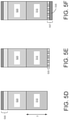
- FIGS. 5A through 5F schematically illustrate a cross-sectional view of portions of a semiconductor substrate as it is being processed at different stages or steps of the method of FIG. 4 to make a diode.
- FIGS. 6A and 6B illustrate example dopant concentrations in a rectangular cross section of an example diode not having a universal contact in its cathode structure.
- FIGS. 7A and 7B illustrate example dopant concentrations in a rectangular cross section of an example diode having a universal contact in its cathode structure.
- FIG. 8 is a graph illustrating simulated reverse recovery currents and voltages for an example diode without a backside p-n junction, and an example diode having a backside p-n junction in its cathode structure.
- FIG. 9A is a graph illustrating simulated reverse recovery currents for a set of diodes having different p-to-n areal ratios in the universal contacts of the diodes.
- FIG. 9B is an exploded view of a portion of the graph of FIG. 9A .
- FIG. 10 is a graph illustrating simulated forward currents (IF) as a function of forward voltage (VF) for a set of diodes having different p-to-n areal ratios in the universal contacts of the diodes.
- FIG. 11 is a graph illustrating simulated reverse load currents (IR) as a function of load voltage (VR) for the same set of diodes as FIG. 10 .
- FIG. 12 is a graph illustrating simulated reverse recovery currents for a diode with no oxide layer included in its universal contact and a diode with an oxide layer covering the p-regions of its universal contact.
- FIG. 13 is a graph illustrating simulated forward currents for the diodes of FIG. 12 .
- a p-i-n diode includes two oppositely doped semiconductor regions that are separated by an undoped or lightly-doped semiconductor drift region. Each of the two oppositely doped semiconductor regions is in electrical contact (ohmic contact) with a respective electrode (i.e., an anode or a cathode) of the device which allows flow of charge carriers (i.e., holes or electrons) into, and out of, the respective doped semiconductor region of the diode.
- a respective electrode i.e., an anode or a cathode
- At least one of the electrodes is configured as a universal contact that allows flow of both holes and electrons) into, and out of, the respective doped semiconductor region of the diode.
- the universal contact to a doped semiconductor region of the diode may have a structure that includes both P-doped semiconductor regions and N-doped semiconductor regions in contact with the respective doped semiconductor region of the diode.
- the P-doped semiconductor regions and N-doped semiconductor regions may be present in different areas of the universal contact.
- a p-to-n areal ratio can be used as a figure of merit to describe a ratio of an area of the universal contact occupied by P-doped semiconductor regions and an area of the universal contact occupied by N-doped semiconductor regions.
- the p-to-n areal ratio is selected in consideration of the reverse current recovery time of the device, and in consideration of the forward current of the device.
- FIG. 1A illustrates an example structure of an example free wheeling diode (e.g., FRD 100 ), in accordance with the principles of the present disclosure.
- FRD 100 may have soft recovery characteristics for use in power switching circuits.
- FRD 100 which may have a p-i-n diode-like structure that includes two oppositely doped semiconductor regions ( 110 , 130 ) that are separated by a semiconductor drift region 120 .
- Semiconductor region 110 may, for example, be a p-doped semiconductor region, and semiconductor region 130 may be an n-doped semiconductor region.
- Semiconductor drift region 120 may, for example, be a semiconductor region that is undoped or is lightly doped compared to the two oppositely doped semiconductor regions 110 , 130 .
- the two oppositely doped semiconductor regions 110 , 130 may be heavily doped because they are used for making electrode structures (e.g., anode structure 112 and cathode structure 132 , respectively) of FRD 100 .
- Anode structure 112 may, for example, be a metal or metal alloy layer that makes ohmic contact with semiconductor region 110 (e.g., a p-doped semiconductor region) allowing transport of holes into semiconductor region 110 .
- semiconductor region 110 e.g., a p-doped semiconductor region
- a device electrode structure may include a universal contact structure 133 interposed between a metal or metal alloy layer 134 and semiconductor region 130 (e.g., n-doped semiconductor region).
- Universal contact structure 133 may include a semiconductor region (e.g., semiconductor region 133 A of opposite polarity to that of semiconductor region 130 ) forming a p-n junction 135 A along at least a part of an interface 135 between universal contact structure 133 and semiconductor region 130 .
- universal contact structure 133 may include at least one pair of semiconductor regions ( 133 A, 133 B) that alternate in a lateral direction (along interface 135 between universal contact structure 133 and semiconductor region 130 ).
- Semiconductor region 133 A may for example, be a heavily P+ doped semiconductor region, while semiconductor region 133 B may for example, be a heavily N+ doped semiconductor region.
- Semiconductor region 133 A (a backside p doped region) forms a p-n junction 135 A (a backside p-n junction) with a part of a lateral area or extent of semiconductor region 130 along interface 135 .
- the semiconductor regions ( 133 A, 133 B) of the universal contact structure 133 may occupy different areas along interface 135 .
- FIG. 1B (which is an exploded partial cross-sectional view of FRD 100 shown in FIG. 1A ) shows, for example, semiconductor region 133 A as being present along a length L 1 of interface 135 , while semiconductor regions 133 B as being present along a different length L 2 of interface 135 .
- semiconductor region 133 A and semiconductor region 133 B of universal contact structure 133 are present (assuming a same depth of the semiconductor regions perpendicular to the plane of FIG. 1B ) in an areal ratio of L 1 :L 2 along interface 135 .
- the areal ratio of semiconductor region 133 A and semiconductor region 133 B along interface 135 may be referred to hereinafter as the p-to-n areal ratio of the universal contact structure 133 .
- Universal contact structure 133 may make a contact with semiconductor region 130 that allows transport of both holes and electrons into semiconductor region 130 .
- the holes may be transported into semiconductor region 130 , for example, via P+ doped semiconductor regions 133 A, and the electrons may be transported into semiconductor region 130 , for example, via N+ doped semiconductor regions 133 B.
- FRD 100 When switching from a conducting to a blocking state, FRD 100 has stored charge (e.g., reverse recovery charge (Qrr)) in, for example, semiconductor drift region 120 , that must first be discharged before FRD 100 blocks reverse current. This discharge takes a finite amount of time known as the reverse recovery time, or t rr .
- charge e.g., reverse recovery charge (Qrr)
- t rr the reverse recovery time
- Cathode structure 132 by allowing transport of holes into FRD 100 via P+ doped semiconductor regions 133 A (in addition to the transport of holes into semiconductor region 110 via the ohmic contact made by anode structure 112 ) would increase the reverse recovery time of FRD 100 over that of a conventional p-i-n diode structure (not shown) with conventional ohmic anode and cathode contacts (i.e., non-universal contacts) by increasing the tail of reverse recovery current.
- FIG. 2 shows schematically a reverse recovery current 210 of FRD 100 , which has a reverse recovery time t rr .
- FIG. 2 also shows schematically, for comparison, a reverse recovery current 220 of a conventional p-i-n diode, which has a comparable reverse recovery time t rr .
- reverse recovery current 210 of FRD 100 has a smooth profile gradually returning to a zero value and hence may be characterized as being a “soft” recovery.
- reverse recovery current 220 of the conventional p-i-n diode has a noisy (i.e., snappy, not smooth) return to a zero value and hence may be characterized as being a “hard” recovery.
- FIG. 3 illustrates FRD 100 with another example cathode structure for a universal contact to a diode, in accordance with the principles of the present disclosure.
- FRD 100 can include a different cathode structure 332 other than cathode structure 132 shown in FIG. 1A .
- Cathode structure 332 while generally similar to cathode structure 132 of FRD 100 (shown in FIG. 1A ), further includes an oxide layer 336 interposed between universal contact structure 133 and metal layer 132 .
- oxide layer 336 may overlay P+ semiconductor region 133 A and may extend partially over N+ semiconductor region 133 B. Oxide layer 336 overlaying P+ semiconductor region 133 A may act as a barrier to the flow of holes, prevent leakage of holes out of FRD 100 through cathode 332 , and further improves the characteristics of the diode.
- FIG. 4 illustrates a method 400 for fabricating an FRD (e.g., FRD 100 ) with soft recovery characteristics.
- FIGS. 5A-5F which may be viewed in conjunction with FIGS. 1A and 1B (and FIG. 3 ), schematically illustrate a cross-sectional view of portions of a semiconductor substrate as it is being processed at different stages or steps of method 400 to make FRD 100 .
- method 400 includes growing an n-type epitaxial layer on a N-type semiconductor substrate (e.g., an N+ doped silicon substrate) ( 410 ).
- the n-type epitaxial layer (which forms a drift region, e.g., semiconductor region 120 of FRD 100 ) may be undoped or lightly doped at a concentration lower than that of the N-type semiconductor substrate
- Method 400 further includes forming an anode structure of the FRD ( 420 ).
- Forming the anode structure may include forming a P+ layer on a top surface of the n-type epitaxial layer and depositing a metal layer on the P+ layer to form an anode structure of FRD 100 .
- the P+ layer may be formed by thermal diffusion, and/or implantation, of p dopant species into the top surface of the n-type epitaxial layer.
- Method 400 further includes back grinding the semiconductor substrate to reduce its thickness ( 430 ).
- the reduced thickness of the back-ground semiconductor substrate may correspond to a thickness of a buffer layer of FRD 100 .
- Method 400 further includes forming a universal contact (e.g., universal contact structure 133 ) on a back surface of the back-ground semiconductor substrate ( 440 ).
- Forming the universal contact may involve a buffer implantation (e.g., of an n dopant such as phosphorus), followed by a p dopant (e.g., boron) implantation into the back surface of the back-ground semiconductor substrate.
- Forming the universal contact may further involve a photolithographic patterning step to delineate the P+ regions 133 A and the N+ regions 133 B of universal contact structure 133 , followed by n dopant (e.g., phosphorus) implantation to form the N+ regions 134 B.
- a laser annealing step may be carried out to activate the foregoing dopants in universal contact structure 133 .
- Method 400 further includes depositing a back metal on a back surface of universal contact structure 133 to form a cathode structure of FRD 100 ( 450 ).
- forming a universal contact on a back surface of the back-ground semiconductor substrate 440 in method 400 may include patterning and depositing an oxide layer (e.g., oxide layer 336 ) over P+ region 133 A and partially over N+ regions 133 B.
- the oxide layer may be deposited before depositing the back metal on the back surface of universal contact structure 133 .
- FIGS. 5A-5F schematically illustrate a cross-sectional view of portions of a semiconductor substrate as it is being processed at different stages or steps of method 400 to make FRD 100 .
- FIG. 5A shows, for example, a portion of a semiconductor substrate 510 that is being processed by method 400 to make FRD 100 .
- semiconductor substrate 510 may be an N+ silicon wafer with resistivity in the range of about 0.001-50 ⁇ cm.
- FIG. 5B shows, for example, at step 410 of method 400 , an epitaxial layer 520 grown on semiconductor substrate 510 .
- epitaxial layer 520 may be a undoped or lightly doped epitaxial layer with a resistivity, for example, in the range of 20-200 ⁇ cm and have a thickness, for example, in a range of about 10-100 ⁇ m.
- FIG. 5C shows, for example, at step 420 of method 400 , formation of an anode structure 530 of FRD 100 .
- Anode structure 530 may, for example, include a P+ layer 532 on a top surface of epitaxial layer 520 and a metal layer 534 deposited on the P+ layer 532 .
- FIG. 5D shows, for example, semiconductor substrate 510 with a reduced thickness T after it has been back ground at step 430 of method 400 ,
- FIG. 5E shows, for example, at step 440 of method 400 , formation of a universal contact 533 (having alternating P doped and N doped regions) on a backside of semiconductor substrate 510 with reduced thickness T.
- FIG. 5F shows, for example, at step 450 of method 400 , a back metal 535 deposited on a back surface of universal contact 533 to form a cathode structure 537 of FRD 100 ( 450 ).
- FIG. 6A is a X-Y plot of a cross-section of diode 610 with a trace line C 1 extending from a top of diode 610 to a bottom of diode 610 .
- An example diode 610 may have a vertical die thickness t of about 0.114 millimeters and a lateral die area (e.g., in a plane perpendicular to FIG. 6A , not shown) of about 11 square millimeters.
- Diode 610 has a conventional cathode structure (i.e. without a backside p-n-junction).
- FIG. 6B is a X-Y plot illustrating dopant concentrations in diode 610 along trace line C 1 .
- FIG. 7A is a X-Y plot of a cross-section of diode 710 with a trace line C 1 extending from a top of diode 710 to a bottom of diode 710 .
- An example diode 710 may have a universal contact including a N+ semiconductor region 712 A and a P+ semiconductor region 722 forming a backside p-n junction 732 .
- Diode 710 may have a vertical die thickness t of about 0.114 millimeters and a lateral die area (e.g., in a plane perpendicular to FIG. 7A , not shown) of about 11 square millimeters.
- FIG. 7B is a X-Y plot illustrating dopant concentrations in the universal contact region of diode 710 along trace line C 1 .
- FIG. 8 is a graph illustrating simulated reverse recovery current 810 and voltage 830 for diode 610 (without a backside p-n junction), and reverse recovery current 820 and voltage 840 for diode 710 (with universal contact including a backside p-n junction in its cathode structure).
- TCAD Technology Computer-Aided Design
- diode 710 exhibits a softer recovery than diode 610 (without a universal contact).
- FIG. 9A shows simulated reverse recovery currents for a set of diodes having different p-to-n areal ratios in the universal contacts of the diodes.
- Reverse recovery current 910 corresponds to a diode having a universal contact p-to-n areal ratio of zero:200 (i.e., a diode without a universal contact);
- reverse recovery current 920 corresponds to a diode having a universal contact p-to-n areal ratio of 50:100;
- reverse recovery current 930 corresponds to a diode having a universal contact p-to-n areal ratio of 100:100; and
- reverse recovery current 940 corresponds to a diode having a universal contact p-to-n areal ratio of 150:100.
- FIG. 9A A portion of FIG. 9A is enclosed in dashed line rectangular box 97 .
- FIG. 9B shows an exploded view of the portion of FIG. 9A is enclosed in the dashed line rectangular box 97 .
- an arrow 91 is overlaid across the reverse recovery current curves as a visual aid to indicate a direction of increasing p-to-n areal ratios (i.e., (zero:100 to 150:100) in the universal contacts of the diodes.
- a length of a tail of the reverse current curve approaching zero is a measure of the softness of the reverse current recovery of the diode.
- a tail 93 of the reverse recovery currents increases in length as the p-to-n areal ratios in the universal contacts of the diodes increase.
- increasing the p-to-n areal ratio in the universal contact of a diode is likely to increase softness of the reverse current recovery of the diode.
- FIG. 10 shows simulated forward currents (IF) as a function of forward voltage (VF) for a set of diodes having different p-to-n areal ratios in the universal contacts of the diodes.
- Forward current 1010 corresponds to a diode having no universal contact (i.e., a diode without a universal contact);
- forward current 1020 corresponds to a diode having a universal contact p-to-n areal ratio of 50:150 (i.e., 0.33:1);
- forward current 1030 corresponds to a diode having a universal contact p-to-n areal ratio of 100:100 (i.e., 1:1);
- forward current 1040 corresponds to a diode having a universal contact p-to-n areal ratio of 150:100 (i.e., 1.5:1).
- FIG. 11 shows simulated reverse load currents (IR) as a function of load voltage (VR) for the same set of diodes as FIG. 10 .
- Reverse load current 1110 corresponds to a diode having no universal contact p-to-n areal ratio (i.e., a diode without a universal contact);
- reverse load current 1120 corresponds to a diode having a universal contact p-to-n areal ratio of 50:150 (i.e., 0.33:1);
- reverse recovery current 1130 corresponds to a diode having a universal contact p-to-n areal ratio of 100:100 (i.e., 1:1);
- reverse recovery current 1140 corresponds to a diode having a universal contact p-to-n areal ratio of 150:100 (i.e., 1.5:1).
- An arrow 92 is overlaid across the forward current curves in FIG. 10 (and the reverse load current curves in FIG. 11 ) as a visual aid to indicate a direction of increasing p-to-n areal ratios (i.e., zero:200 to 150:100) in the universal contacts of the diodes.
- the forward voltages of the diodes increase as the p-to-n areal ratio in the universal contacts of the diode increases (e.g., from zero:200 to 150:50).
- the reverse load current curves ( 1110 , 1120 , 1130 , and 1140 ) for different p-to-n areal ratios are bunched up together and substantially overlap each over a voltage range of 1500V to 170V.
- FIG. 12 shows a simulated reverse recovery current 1210 for a diode with no oxide layer included in its universal contact (which, e.g., has a p-to-n areal ratio of 75:25 (i.e., 3:1)).
- FIG. 12 also shows a simulated reverse recovery current 1220 for a diode with an oxide layer covering the p-regions of its universal contact (which, e.g., has a p-to-n areal ratio of 50:50 (i.e., 1:1)).
- FIG. 13 shows a simulated forward current 1310 for the diode with no oxide layer included in its universal contact (which, e.g., has a p-to-n areal ratio of 75:25 (i.e., 3:1)).
- FIG. 13 also shows a simulated forward current 1320 for the diode with an oxide layer cover the p-regions of its universal contact (which, e.g., has a p-to-n areal ratio of 50:50 (i.e., 1:1)).
- the simulated currents and voltages described above with reference to FIG. 6A through FIG. 13 demonstrate that incorporating a universal contact including a backside p-n junction in the cathode structure improves the soft reverse current recovery characteristics of the diode. Including an oxide layer over P-regions of the universal contact additionally improves reverse current recovery of the diode.
- a singular form may, unless definitely indicating a particular case in terms of the context, include a plural form.
- Spatially relative terms e.g., over, above, upper, under, beneath, below, lower, and so forth
- the relative terms above and below can, respectively, include vertically above and vertically below.
- the term adjacent can include laterally adjacent to or horizontally adjacent to.
- Implementations of the various techniques described herein may be implemented in (e.g., included in) digital electronic circuitry, or in computer hardware, firmware, software, or in combinations of them. Portions of methods also may be performed by, and an apparatus may be implemented as, special purpose logic circuitry, e.g., an FPGA (field programmable gate array) or an ASIC (application-specific integrated circuit).
- FPGA field programmable gate array
- ASIC application-specific integrated circuit
- Implementations may be implemented in a computing system that includes an industrial motor driver, a solar inverter, ballast, a general-purpose half-bridge topology, an auxiliary and/or traction motor inverter driver, a switching mode power supply, an on-board charger, an uninterruptible power supply (UPS), a back-end component, e.g., as a data server, or that includes a middleware component, e.g., an application server, or that includes a front-end component, e.g., a client computer having a graphical user interface or a Web browser through which a user can interact with an implementation, or any combination of such back-end, middleware, or front-end components.
- Components may be interconnected by any form or medium of digital data communication, e.g., a communication network. Examples of communication networks include a local area network (LAN) and a wide area network (WAN), e.g., the Internet.
- LAN local area network
- WAN wide area network
Abstract
Description
Claims (18)
Priority Applications (3)
| Application Number | Priority Date | Filing Date | Title |
|---|---|---|---|
| US16/667,631 US11233158B2 (en) | 2019-08-16 | 2019-10-29 | Semiconductor power device and method for manufacture |
| DE102020004721.1A DE102020004721A1 (en) | 2019-08-16 | 2020-08-04 | SEMICONDUCTOR DEVICE AND METHOD OF MANUFACTURING |
| CN202010806477.4A CN112397578A (en) | 2019-08-16 | 2020-08-12 | Semiconductor power device and method for manufacturing the same |
Applications Claiming Priority (2)
| Application Number | Priority Date | Filing Date | Title |
|---|---|---|---|
| US201962887759P | 2019-08-16 | 2019-08-16 | |
| US16/667,631 US11233158B2 (en) | 2019-08-16 | 2019-10-29 | Semiconductor power device and method for manufacture |
Publications (2)
| Publication Number | Publication Date |
|---|---|
| US20210050458A1 US20210050458A1 (en) | 2021-02-18 |
| US11233158B2 true US11233158B2 (en) | 2022-01-25 |
Family
ID=74239609
Family Applications (1)
| Application Number | Title | Priority Date | Filing Date |
|---|---|---|---|
| US16/667,631 Active 2039-12-24 US11233158B2 (en) | 2019-08-16 | 2019-10-29 | Semiconductor power device and method for manufacture |
Country Status (2)
| Country | Link |
|---|---|
| US (1) | US11233158B2 (en) |
| DE (1) | DE102020004721A1 (en) |
Families Citing this family (1)
| Publication number | Priority date | Publication date | Assignee | Title |
|---|---|---|---|---|
| CN114496782A (en) * | 2022-03-28 | 2022-05-13 | 绍兴中芯集成电路制造股份有限公司 | Manufacturing method of fast recovery diode and fast recovery diode |
Citations (5)
| Publication number | Priority date | Publication date | Assignee | Title |
|---|---|---|---|---|
| US20120267681A1 (en) * | 2009-11-02 | 2012-10-25 | Fuji Electric Co., Ltd. | Semiconductor device and method for manufacturing semiconductor device |
| US20160163654A1 (en) * | 2014-12-03 | 2016-06-09 | Renesas Electronics Corporation | Semiconductor device |
| US20170110449A1 (en) * | 2015-10-19 | 2017-04-20 | Kabushiki Kaisha Toshiba | Semiconductor device and method of manufacturing semiconductor device |
| US20190287963A1 (en) * | 2018-03-15 | 2019-09-19 | Toyota Jidosha Kabushiki Kaisha | Semiconductor device |
| US20200105874A1 (en) * | 2018-10-01 | 2020-04-02 | Ipower Semiconductor | Back side dopant activation in field stop igbt |
-
2019
- 2019-10-29 US US16/667,631 patent/US11233158B2/en active Active
-
2020
- 2020-08-04 DE DE102020004721.1A patent/DE102020004721A1/en active Pending
Patent Citations (5)
| Publication number | Priority date | Publication date | Assignee | Title |
|---|---|---|---|---|
| US20120267681A1 (en) * | 2009-11-02 | 2012-10-25 | Fuji Electric Co., Ltd. | Semiconductor device and method for manufacturing semiconductor device |
| US20160163654A1 (en) * | 2014-12-03 | 2016-06-09 | Renesas Electronics Corporation | Semiconductor device |
| US20170110449A1 (en) * | 2015-10-19 | 2017-04-20 | Kabushiki Kaisha Toshiba | Semiconductor device and method of manufacturing semiconductor device |
| US20190287963A1 (en) * | 2018-03-15 | 2019-09-19 | Toyota Jidosha Kabushiki Kaisha | Semiconductor device |
| US20200105874A1 (en) * | 2018-10-01 | 2020-04-02 | Ipower Semiconductor | Back side dopant activation in field stop igbt |
Non-Patent Citations (2)
| Title |
|---|
| M.T. Rahimo, and N.Y.A. Shammas, "A review on fast power diode development and modern novel structures," IEE Colloquium on New Developments in Power Semiconductor Devices (Digest No. 1996 /046, Jun. 21-26, 1997, London, UK). |
| Y. Amemiya, T. Sugeta, and Y. Mizushima, "Novel low-loss and high speed diode utilizing an "Ideal" ohmic contact," IEEE Transactions on Electron Devices (vol. ED-29, No. 2, Feb. 1982). |
Also Published As
| Publication number | Publication date |
|---|---|
| DE102020004721A1 (en) | 2021-02-18 |
| US20210050458A1 (en) | 2021-02-18 |
Similar Documents
| Publication | Publication Date | Title |
|---|---|---|
| US9276137B2 (en) | Diode and semiconductor device including built-in diode | |
| US9947741B2 (en) | Field-effect semiconductor device having pillar regions of different conductivity type arranged in an active area | |
| US9263515B2 (en) | Super-junction schottky PIN diode | |
| US8884360B2 (en) | Semiconductor device with improved robustness | |
| JP3417013B2 (en) | Insulated gate bipolar transistor | |
| US11398472B2 (en) | RC IGBT with an IGBT section and a diode section | |
| US20130207222A1 (en) | Super-junction schottky oxide pin diode having thin p-type layers under the schottky contact | |
| US9620637B2 (en) | Semiconductor device comprising a gate electrode connected to a source terminal | |
| US10847660B2 (en) | Trench semiconductor device having multiple active trench depths and method | |
| US6919587B2 (en) | Low-capacitance bidirectional protection device | |
| US20160260844A1 (en) | Trench semiconductor device having multiple trench depths and method | |
| CN104218087A (en) | Semiconductor Device and Manufacturing Method Therefor | |
| US20230119046A1 (en) | Low leakage schottky diode | |
| CN112201690A (en) | MOSFET transistor | |
| US9679890B2 (en) | Junction-less insulated gate current limiter device | |
| US10930796B2 (en) | Merged p-intrinsic-N (PIN) Schottky diode | |
| US11233158B2 (en) | Semiconductor power device and method for manufacture | |
| JPH05226638A (en) | Semiconductor device | |
| CN112397578A (en) | Semiconductor power device and method for manufacturing the same | |
| US20150115351A1 (en) | Integrated Circuit and Method of Manufacturing an Integrated Circuit | |
| CN108475703B (en) | Silicon carbide semiconductor device | |
| US11444158B2 (en) | Semiconductor device including an anode contact region having a varied doping concentration | |
| US20220375923A1 (en) | Conductivity reducing features in an integrated circuit | |
| JPH05259437A (en) | Semiconductor device | |
| KR100496105B1 (en) | Driving method and driving circuit of electrostatic induction semiconductor device and electrostatic induction semiconductor device |
Legal Events
| Date | Code | Title | Description |
|---|---|---|---|
| AS | Assignment |
Owner name: SEMICONDUCTOR COMPONENTS INDUSTRIES, LLC, ARIZONA Free format text: ASSIGNMENT OF ASSIGNORS INTEREST;ASSIGNOR:LIU, MINGJIAO;REEL/FRAME:050856/0351 Effective date: 20190815 |
|
| FEPP | Fee payment procedure |
Free format text: ENTITY STATUS SET TO UNDISCOUNTED (ORIGINAL EVENT CODE: BIG.); ENTITY STATUS OF PATENT OWNER: LARGE ENTITY |
|
| AS | Assignment |
Owner name: DEUTSCHE BANK AG NEW YORK BRANCH, AS COLLATERAL AGENT, NEW YORK Free format text: SECURITY INTEREST;ASSIGNORS:SEMICONDUCTOR COMPONENTS INDUSTRIES, LLC;FAIRCHILD SEMICONDUCTOR CORPORATION;ON SEMICONDUCTOR CONNECTIVITY SOLUTIONS, INC.;REEL/FRAME:054090/0617 Effective date: 20200213 |
|
| STPP | Information on status: patent application and granting procedure in general |
Free format text: NON FINAL ACTION MAILED |
|
| STPP | Information on status: patent application and granting procedure in general |
Free format text: RESPONSE TO NON-FINAL OFFICE ACTION ENTERED AND FORWARDED TO EXAMINER |
|
| STPP | Information on status: patent application and granting procedure in general |
Free format text: NOTICE OF ALLOWANCE MAILED -- APPLICATION RECEIVED IN OFFICE OF PUBLICATIONS |
|
| STPP | Information on status: patent application and granting procedure in general |
Free format text: AWAITING TC RESP, ISSUE FEE PAYMENT VERIFIED |
|
| STPP | Information on status: patent application and granting procedure in general |
Free format text: PUBLICATIONS -- ISSUE FEE PAYMENT VERIFIED |
|
| STCF | Information on status: patent grant |
Free format text: PATENTED CASE |
|
| AS | Assignment |
Owner name: FAIRCHILD SEMICONDUCTOR CORPORATION, ARIZONA Free format text: RELEASE OF SECURITY INTEREST IN PATENTS RECORDED AT REEL 054090, FRAME 0617;ASSIGNOR:DEUTSCHE BANK AG NEW YORK BRANCH, AS COLLATERAL AGENT;REEL/FRAME:064081/0167 Effective date: 20230622 Owner name: SEMICONDUCTOR COMPONENTS INDUSTRIES, LLC, ARIZONA Free format text: RELEASE OF SECURITY INTEREST IN PATENTS RECORDED AT REEL 054090, FRAME 0617;ASSIGNOR:DEUTSCHE BANK AG NEW YORK BRANCH, AS COLLATERAL AGENT;REEL/FRAME:064081/0167 Effective date: 20230622 |