US11227946B2 - Trench MOSFET contacts - Google Patents
Trench MOSFET contacts Download PDFInfo
- Publication number
- US11227946B2 US11227946B2 US16/825,945 US202016825945A US11227946B2 US 11227946 B2 US11227946 B2 US 11227946B2 US 202016825945 A US202016825945 A US 202016825945A US 11227946 B2 US11227946 B2 US 11227946B2
- Authority
- US
- United States
- Prior art keywords
- trenches
- type
- shield
- contact
- contact area
- Prior art date
- Legal status (The legal status is an assumption and is not a legal conclusion. Google has not performed a legal analysis and makes no representation as to the accuracy of the status listed.)
- Active, expires
Links
Images


Classifications
-
- H01L29/7813—
-
- H—ELECTRICITY
- H10—SEMICONDUCTOR DEVICES; ELECTRIC SOLID-STATE DEVICES NOT OTHERWISE PROVIDED FOR
- H10D—INORGANIC ELECTRIC SEMICONDUCTOR DEVICES
- H10D64/00—Electrodes of devices having potential barriers
- H10D64/111—Field plates
- H10D64/117—Recessed field plates, e.g. trench field plates or buried field plates
-
- H01L29/41766—
-
- H01L29/66734—
-
- H—ELECTRICITY
- H10—SEMICONDUCTOR DEVICES; ELECTRIC SOLID-STATE DEVICES NOT OTHERWISE PROVIDED FOR
- H10D—INORGANIC ELECTRIC SEMICONDUCTOR DEVICES
- H10D30/00—Field-effect transistors [FET]
- H10D30/01—Manufacture or treatment
- H10D30/021—Manufacture or treatment of FETs having insulated gates [IGFET]
- H10D30/028—Manufacture or treatment of FETs having insulated gates [IGFET] of double-diffused metal oxide semiconductor [DMOS] FETs
- H10D30/0291—Manufacture or treatment of FETs having insulated gates [IGFET] of double-diffused metal oxide semiconductor [DMOS] FETs of vertical DMOS [VDMOS] FETs
- H10D30/0297—Manufacture or treatment of FETs having insulated gates [IGFET] of double-diffused metal oxide semiconductor [DMOS] FETs of vertical DMOS [VDMOS] FETs using recessing of the gate electrodes, e.g. to form trench gate electrodes
-
- H—ELECTRICITY
- H10—SEMICONDUCTOR DEVICES; ELECTRIC SOLID-STATE DEVICES NOT OTHERWISE PROVIDED FOR
- H10D—INORGANIC ELECTRIC SEMICONDUCTOR DEVICES
- H10D30/00—Field-effect transistors [FET]
- H10D30/60—Insulated-gate field-effect transistors [IGFET]
- H10D30/64—Double-diffused metal-oxide semiconductor [DMOS] FETs
- H10D30/66—Vertical DMOS [VDMOS] FETs
- H10D30/668—Vertical DMOS [VDMOS] FETs having trench gate electrodes, e.g. UMOS transistors
-
- H—ELECTRICITY
- H10—SEMICONDUCTOR DEVICES; ELECTRIC SOLID-STATE DEVICES NOT OTHERWISE PROVIDED FOR
- H10D—INORGANIC ELECTRIC SEMICONDUCTOR DEVICES
- H10D62/00—Semiconductor bodies, or regions thereof, of devices having potential barriers
- H10D62/10—Shapes, relative sizes or dispositions of the regions of the semiconductor bodies; Shapes of the semiconductor bodies
- H10D62/124—Shapes, relative sizes or dispositions of the regions of semiconductor bodies or of junctions between the regions
- H10D62/126—Top-view geometrical layouts of the regions or the junctions
- H10D62/127—Top-view geometrical layouts of the regions or the junctions of cellular field-effect devices, e.g. multicellular DMOS transistors or IGBTs
-
- H—ELECTRICITY
- H10—SEMICONDUCTOR DEVICES; ELECTRIC SOLID-STATE DEVICES NOT OTHERWISE PROVIDED FOR
- H10D—INORGANIC ELECTRIC SEMICONDUCTOR DEVICES
- H10D64/00—Electrodes of devices having potential barriers
- H10D64/20—Electrodes characterised by their shapes, relative sizes or dispositions
- H10D64/23—Electrodes carrying the current to be rectified, amplified, oscillated or switched, e.g. sources, drains, anodes or cathodes
- H10D64/251—Source or drain electrodes for field-effect devices
- H10D64/256—Source or drain electrodes for field-effect devices for lateral devices wherein the source or drain electrodes are recessed in semiconductor bodies
-
- H—ELECTRICITY
- H10—SEMICONDUCTOR DEVICES; ELECTRIC SOLID-STATE DEVICES NOT OTHERWISE PROVIDED FOR
- H10D—INORGANIC ELECTRIC SEMICONDUCTOR DEVICES
- H10D64/00—Electrodes of devices having potential barriers
- H10D64/20—Electrodes characterised by their shapes, relative sizes or dispositions
- H10D64/27—Electrodes not carrying the current to be rectified, amplified, oscillated or switched, e.g. gates
- H10D64/311—Gate electrodes for field-effect devices
- H10D64/411—Gate electrodes for field-effect devices for FETs
- H10D64/511—Gate electrodes for field-effect devices for FETs for IGFETs
- H10D64/512—Disposition of the gate electrodes, e.g. buried gates
- H10D64/513—Disposition of the gate electrodes, e.g. buried gates within recesses in the substrate, e.g. trench gates, groove gates or buried gates
-
- H—ELECTRICITY
- H10—SEMICONDUCTOR DEVICES; ELECTRIC SOLID-STATE DEVICES NOT OTHERWISE PROVIDED FOR
- H10D—INORGANIC ELECTRIC SEMICONDUCTOR DEVICES
- H10D64/00—Electrodes of devices having potential barriers
- H10D64/20—Electrodes characterised by their shapes, relative sizes or dispositions
- H10D64/27—Electrodes not carrying the current to be rectified, amplified, oscillated or switched, e.g. gates
- H10D64/311—Gate electrodes for field-effect devices
- H10D64/411—Gate electrodes for field-effect devices for FETs
- H10D64/511—Gate electrodes for field-effect devices for FETs for IGFETs
- H10D64/517—Gate electrodes for field-effect devices for FETs for IGFETs characterised by the conducting layers
- H10D64/519—Gate electrodes for field-effect devices for FETs for IGFETs characterised by the conducting layers characterised by their top-view geometrical layouts
-
- H—ELECTRICITY
- H10—SEMICONDUCTOR DEVICES; ELECTRIC SOLID-STATE DEVICES NOT OTHERWISE PROVIDED FOR
- H10D—INORGANIC ELECTRIC SEMICONDUCTOR DEVICES
- H10D84/00—Integrated devices formed in or on semiconductor substrates that comprise only semiconducting layers, e.g. on Si wafers or on GaAs-on-Si wafers
- H10D84/80—Integrated devices formed in or on semiconductor substrates that comprise only semiconducting layers, e.g. on Si wafers or on GaAs-on-Si wafers characterised by the integration of at least one component covered by groups H10D12/00 or H10D30/00, e.g. integration of IGFETs
- H10D84/82—Integrated devices formed in or on semiconductor substrates that comprise only semiconducting layers, e.g. on Si wafers or on GaAs-on-Si wafers characterised by the integration of at least one component covered by groups H10D12/00 or H10D30/00, e.g. integration of IGFETs of only field-effect components
- H10D84/83—Integrated devices formed in or on semiconductor substrates that comprise only semiconducting layers, e.g. on Si wafers or on GaAs-on-Si wafers characterised by the integration of at least one component covered by groups H10D12/00 or H10D30/00, e.g. integration of IGFETs of only field-effect components of only insulated-gate FETs [IGFET]
Definitions
- This description relates to contacts in a shielded gate trench MOSFET.
- semiconductor device e.g., device cell dimensions
- gate and shield contacts in as semiconductor device (e.g., a shield gate shielded gate trench MOSFET).
- semiconductor device e.g., a shield gate shielded gate trench MOSFET
- Different lithography design rules may be used for active areas and contact areas of the semiconductor device.
- charge in the drift regions of the MOSFET has to be well controlled and balanced in both the active areas and the contact areas to avoid adversely affecting the breakdown voltage of the device.
- FIG. 1A is a top view of a portion of an example contact structure layout in a semiconductor region of a trench MOSFET device, in accordance with the principles of the present disclosure.
- FIG. 1B is an illustration of a cross-sectional view of a portion of the device of FIG. 1A .
- FIG. 1C is an illustration of a cross-sectional view of a portion of the device of FIG. 1A .
- FIG. 1D is an illustration of a cross-sectional view of a portion of the device of FIG. 1A .
- FIG. 2 is an illustration of an example contact structure layout of a device configured for external gate feed.
- FIG. 3 is an example contact structure layout of a device configured for internal gate feed.
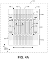
- FIG. 4A is an illustration of an example contact structure of device including active areas and a shield contact area.
- FIG. 4B is an illustration of a cross-sectional view of a portion of the device of FIG. 4A .
- FIG. 5A is an illustration of an example contact structure layout of device that has different device cell pitches and trench widths in an active area and in a shield contact area, and includes gate pass through features.
- FIG. 5B is an illustration of a cross-sectional view of a portion of the device of FIG. 5A .
- FIG. 6 is an illustration of an example method for making electrical contacts to active elements (e.g., gate electrodes, shield electrodes, source regions, body regions, etc.) of a trench MOSFET device.
- active elements e.g., gate electrodes, shield electrodes, source regions, body regions, etc.
- MOSFET Metal oxide semiconductor field effect transistor
- a gate electrode provides turn-on and turn-off control of the device in response to an applied gate voltage.
- turn-on occurs when a conductive N-type inversion layer (i.e., channel region) is formed in a p-type body region in response to a positive gate voltage, which exceeds an inherent threshold voltage.
- the inversion layer connects N-type source regions to N-type drain regions and allows for majority carrier conduction between these regions.
- a gate electrode is formed in a trench that extends downward (e.g., vertically downward) from a major surface of a semiconductor material (also can be referred to as a semiconductor region) such as silicon. Further, a shield electrode may be formed below the gate electrode in the trench (and insulated via an inter-electrode dielectric).
- Current flow in a trench MOSFET device is primarily vertical (e.g., in an N doped drift region) and, as a result, device cells can be more densely packed.
- a device cell may, for example, include a trench that contains the gate electrode and an adjoining mesa that contains the drain, source, body, and channel regions of the device.
- An example trench MOSFET device may include an array of hundreds or thousands of device cells (each including a trench and an adjoining mesa).
- a device cell may be referred to herein as a trench-mesa cell because each device cell geometrically includes a trench and a mesa (or two half mesas) structures.
- P-doped regions are formed as body regions underneath the source regions alongside N-doped drift regions as a charge balancing mechanism.
- the charge balancing mechanism compensates the charge in the surrounding N regions under reverse bias and enables further reductions in the on-resistance of the devices.
- a new generation of trench MOSFETS may have a target cell pitch that are fractions of a micron (e.g., about 0.65 ⁇ m) and a mesa width approximately half of the target cell pitch (e.g., of about 0.32 ⁇ m).
- contact lithography used for making gate, source and shield contacts is limited in resolution (e.g., limited to 180 nm). Smaller contact sizes for the new generation of MOSFETS may require use of a high resolution (e.g., 193 nm) lithography scanner, which can increase cost significantly.
- making gate, source and shield contacts can require additional masks/process steps, which increases complexity and cost.
- the narrow mesa widths for the gate and shield contacts may increase charge imbalance compared to earlier generations of trench MOSFETS having wider mesa widths.
- the disclosure describes contact structures that can preserve charge balance in the new generation of trench MOSFETS (even when the contact structures are fabricated using contact lithography).
- a larger device cell pitch is used in a contact area (e.g., gate contact area, shield contact area) of the device than the device cell pitch in the active area of device.
- a trench-mesa cell in the contact area is wider than a trench-mesa cell of the active region.
- a wider trench is used in the device cell in the contact area than the trench used in the device cell in the active area to increase the cell pitch in the contact area.
- the mesa used in the device cell in the contact area may have the same width (e.g., substantially same width) or different width (e.g., wider, narrower) as the mesa used in the device cell in the active area.
- having mesas with the same width enables processing (e.g., P High Voltage (PHV) implantation) of the mesas in the contact area and the active area with a same device fabrication mask in a same processing step (e.g., implantation, diffusion).
- PHI P High Voltage
- FIG. 1A shows, in an X-Y plane of the page, a top view of a portion of an example contact structure layout 101 in a semiconductor region 102 of a trench MOSFET device 100 , in accordance with the principles of the present disclosure.
- Contact structure layout 101 may be used for an internal gate bus area in the body of the array of all device cells in device 100 .
- the relative orientations or coordinates of features (e.g., trenches 130 , 140 ) of the trench MOSFET device 100 may be described herein with reference to the X axis and Y axis shown, for example, on the page of FIG. 1A .
- the direction perpendicular to the X-Y plane of the page e.g., the Z axis
- the vertical direction or axis e.g., the Z axis
- a limited number of trenches/device cells e.g., 6-7 trenches/device cells of the arrays of trenches/device cells in device 100 are shown in FIG. 1A .
- an actual MOSFET device may include arrays of hundreds or thousands of trenches/device cells, which may be obtained, for example, by repeating (e.g., in the X direction) the limited array structures shown in example layout 101 .
- Layout 101 shows active areas 110 A and 110 B (collectively can be referred to as active areas 110 ) and a gate contact area 120 of MOSFET device 100 .
- Each of the active areas 110 is separated from gate contact area 120 by a separation trench (e.g., separation trench 136 A, 136 B) (aligned with the X direction) formed in semiconductor region 102 .
- active area 110 A is disposed, for example, on a first side of separation trench (e.g., separation trench 136 A) and gate contact area 120 is disposed on a second side of separation trench 136 A.
- Active area 110 A and gate contact area 120 may have a same width W (in the X direction) along separation trench 136 A.
- Active areas 110 includes a plurality of trenches of a first type (e.g., an array of trenches 130 ), each of which has a length parallel to longitudinal axis 191 (in the Y direction) and has a width (e.g., width W 1 t , FIG. 1B ) aligned parallel to separation trench 136 A (in the X direction).
- a first type e.g., an array of trenches 130
- Each of the plurality of trenches 130 of the first type is aligned perpendicular to and has a first longitudinal end terminating at separation trench 136 A.
- Active area mesas 132 are formed between pairs of trenches 130 in the active areas 110 .
- Each active area mesa 132 may have a width (in the X direction, e.g., width W 1 m , FIG. 1B ) aligned parallel to separation trench 136 A.
- An active area mesa 132 may include a source contact region or element 134 of device 100 that is exposed in the X-Y plane of the device.
- Gate contact area 120 includes a plurality of trenches of a second type (e.g., array of trenches 140 ), each of which has a length parallel to longitudinal axis 193 (in the Y direction) and has a width (e.g., width W 2 t , FIG. 1C ) aligned parallel to separation trench 136 A (in the X direction).
- Each of the plurality of trenches 140 is aligned perpendicular to and has a first longitudinal end terminating at separation trench 136 A.
- each of the plurality of trenches 140 of the second type is also aligned perpendicular to another separation trench 136 B and has a second longitudinal end terminating at separation trench 136 B.
- a trench 140 may include gate electrode structures (i.e., gate poly and gate oxide) that extend from the active area into the gate contact area.
- Trench 140 may include a gate electrode contact element 144 of device 100 that is exposed in the X-Y plane of the device for contacting the gate electrode structures in trench 140 .
- Gate contact area mesas 142 are formed between pairs of trenches 140 in gate contact area 120 .
- Each gate contact area mesa 142 may have a width (in the X direction e.g., width W 2 m , FIG. 1C ) aligned parallel to separation trench 136 .
- a gate contact area mesa 142 may include a source or body region contact element 135 of device 100 that is exposed in the X-Y plane of the device.
- a conductive contact layer may overlay portions of active area 110 to establish electrical contact with source contact regions or elements 134 of device 100 that are exposed in mesas 132 .
- Source metal layer 150 may also extend over portions of gate contact area 120 establishing electrical contact with source or body region contact elements 135 of device 100 that are exposed in mesas 142 .
- Source metal layer 150 may be made of metal or metal alloys used for making source contacts in MOSFET devices.
- Gate contact layer 160 may overlay portions of gate contact area 120 to establish electrical contact with gate electrode contact elements 144 that are exposed in trenches 140 of device 100 .
- Gate contact layer 160 may be made of conductive materials, for example, doped polysilicon, metal, or metal alloys.
- a device cell may, for example, include a trench and an adjoining mesa.
- the array of trenches 130 and mesas 132 in active areas 110 A, 110 B shown in FIG. 1A may correspond to a cell pitch 190
- the array of trenches 140 and mesas 142 in gate contact area 120 shown in FIG. 1A may correspond to a cell pitch 192 .
- cell pitch 192 in gate contact area 120 is increased and made larger than cell pitch 190 by including wider trenches (e.g.
- trenches 140 for making contacts, while keeping the widths of mesas 142 in gate contact area 120 to be the same as (e.g., be about the same as) the widths of mesas 132 in active area 110 .
- the longitudinal axes (e.g., longitudinal axes 191 ) of trenches 130 in active area 110 are generally offset (in the X direction) from the longitudinal axes (e.g., longitudinal axes 193 ) of trenches 140 in gate contact area 120 .
- an integer number of device cells (N) in active areas 110 correspond to a reduced integer number (e.g., N-i) of wider device cells in the gate contact area 120 .
- the number of device cells in the active areas 110 over width W can be greater than the number of device cells in the gate contact area 120 .
- the number of mesas (e.g., mesas 132 ) in the active areas 110 over width W can be greater than the number of mesas (e.g., mesas 142 ) in the gate contact area 120 .
- the number of trenches (e.g., trenches 130 ) in the active areas 110 over width W can be greater than the number of trenches (e.g., trenches 140 ) in the gate contact area 120 .
- a number of the trenches 140 in the contact area 120 on a first side of the separation trench 136 A can be less than a number of the trenches 130 in the active area 110 A terminating on a second side of the separation trench 136 A per width W of the separation trench 136 A (e.g., per unit length of the separation trench).
- the mesa widths in the contact area may allow fabrication of a P High Voltage (PHV) body region in the gate (and shield) contact areas, with gate oxide around gate poly, in the same manner as the fabrication of body regions in the active areas of device 100 .
- the gate electrode structures (i.e., gate poly and gate oxide around the gate poly) in the trenches in the gate (and shield) contact areas may extend from, and be the same as, the gate electrode structures in the active areas of device 100 .
- the mesas in the gate contact area 120 may function the same as the mesas in the active areas 110 resulting in similar charge balance and breakdown characteristics (e.g., BVDSS) in the active and contact areas of device 100 .
- the P High Voltage (PHV) body region in a contact area mesa may be formed using the same mask and processing step (e.g., implantation, diffusion, etc.) used to form a P High Voltage (PHV) body region in the active area mesa of the same width.
- the mesa widths (e.g., W 2 m , FIG. 1C ) in gate contact area 120 need not be exactly the same as the mesa widths (e.g., W 1 m , FIG. 1B ) in active area 110 .
- fabricated trenches 140 being wider than trenches 130
- fabricated inter-trench mesas 142 can be narrower than fabricated inter-trench mesas 132 .
- gate contact area 120 may be adjusted (e.g., made narrower) to compensate for a greater depth (along the Z direction) that the wider trenches 140 are expected to have than a depth (along the Z direction) of the narrower trenches 130 in active area 110 .
- width compensation may be used, for example, to form narrower mesa structures between deeper trenches in the contact area that can have the same breakdown characteristics (e.g., after same body region formation processes) as the relatively wider mesa structures formed between the shallower trenches in the active areas of device 100 .
- the example layout 101 shown in FIG. 1A can be an instance of a design element that can be used within a circuit design of a device.
- multiple instances of the example layout 101 shown in FIG. 1A can be abutted (coupled at the separation trenches 136 A, 136 B) and included within a device.
- the example layout 101 can be repeated many times within a device to form portions of the array of all device cells in the device.
- FIG. 1B shows a cross-sectional view of a portion of device 100 in the Z-Y plane across, for example, three trenches 130 in active area 110 (taken along line B-B in FIG. 1A ).
- trench 130 may include a gate electrode 131 , and a shield electrode 133 .
- Trench 130 may be filled with insulating material 130 a surrounding gate electrode 131 and shield electrode 133 .
- mesas 132 formed between pairs of trenches 130 in the active area of device 100 may include MOSFET device regions such as N- drift region 132 a , P- body region 132 b , and source region 132 c .
- Mesa 132 may include exposed source contact regions or elements 134 of device 100 that are in electrical contact with source metal layer 150 . As shown in FIG. 1B , trench 130 may have a width W 1 t , and mesa 132 may have a width W 1 m.
- FIG. 1C shows a cross-sectional view of a portion of device 100 in the Z-Y plane across, for example, two trenches 140 in gate contact area 120 (taken along line C-C in FIG. 1A ).
- trench 140 may include a gate electrode 131 , and a shield electrode 133 .
- Trench 140 may be filled with insulating material 130 a surrounding gate electrode 131 and shield electrode 133 .
- mesas 142 (formed between pairs of trenches 140 ) in the gate contact area of device 100 may include MOSFET device regions such as N- drift region 132 a and P- body region 132 b .
- a mesa 142 may include exposed source or body region contact element 135 of device 100 that is in electrical contact with source metal layer 150 .
- Insulating material 130 a may isolate gate electrode 131 from source metal layer 150 .
- trench 140 may have a width W 2 t
- mesa 142 may have a width W 2 m
- mesa 142 width W 2 m may be about the same as mesa 132 width W 1 m ( FIG. 1B )
- N- drift region 142 a and P- body region 142 b in mesa 142 may have the same characteristics as N- drift region 132 a and P-body region 132 b in mesa 132 ( FIG. 1B ).
- FIG. 1D shows a cross-sectional view of a portion of device 100 in the Z-Y plane across, for example, two trenches 140 in gate contact area 120 (taken along line D-D in FIG. 1A ).
- trench 140 may include a gate electrode 131 , and a shield electrode 133 .
- Trench 140 may be filled with insulating material 130 a surrounding gate electrode 131 and shield electrode 133 .
- Insulating material 130 a may extend over adjoining mesa 142 .
- a mesa 142 (formed between a pair of trenches 140 ) in the gate contact area 120 of device 100 may include MOSFET device regions such as N- drift region 142 a and P- body region 142 b.
- a trench 140 may include exposed gate electrode contact element 144 of device 100 .
- Exposed gate electrode contact element 144 may be electrically connected to gate electrodes (e.g., gates 131 , FIGS. 1B through 1D ) of device 100 disposed in trenches 130 in active area 110 .
- Exposed gate electrode contact element 144 can be in electrical contact with gate metal layer 160 , as shown in FIG. 1D .
- device 100 may not include shield electrodes and gates 131 may be disposed on a thick bottom dielectric without a shield electrode in trenches 140 .
- device 100 may include shield electrodes (e.g., shield electrodes 133 , FIGS. 1B through 1D ) disposed in trenches 140 below the gate electrodes. Contact structure layouts for shield electrodes 133 are described below with reference to FIGS. 4A through 5B .
- trenches 140 in gate contact area 120 have first longitudinal ends which terminate at separation trench 136 A that has an active area 110 A on the opposite side across the separation trench 136 A, and have second longitudinal ends that terminate at separation trench 136 B, which has another active area 110 B on the opposite side across the separation trench 136 B.
- gate contact area 120 has active areas (e.g., active areas 110 A, 110 B) on both longitudinal ends of trenches 140 .
- other structures may be used to terminate the longitudinal ends of trenches 140 in gate contact area 120 .
- FIG. 2 shows an example contact structure layout 201 in which, like in layout 101 of FIG.
- first longitudinal ends of trenches 140 terminate at separation trench 136 A which separates gate contact area 120 from active area 110 C.
- the second longitudinal ends of trenches 140 terminate at a gate termination trench 236 that does not have an active area on the other side.
- gate contact area 120 is adjacent to a single active area 110 A of device 100 in layout 201 , while in layout 101 ( FIG. 1A ) gate contact area 120 is between (e.g., disposed between) two active areas 110 (e.g., active areas 110 A, 110 B) of device 100 .
- gate termination trench 236 which may be substantially parallel to separation trench 136 A, may be disposed in a shield region or section 270 of device 100 .
- the dimensions of shield section 270 may correspond to a mask used in trench MOSFET device fabrication processes, to define an area where the shield conductor is brought up close to the surface of the device.
- Layout 201 may be used for a gate bus contact area with the shield conductor (e.g., shield poly) terminating an end of the array of all device cells in device 100 .
- Layout 201 may be used at the edge (or top and bottom) of the array of all device cells for a one-sided gate contact.
- the gate termination arrangement of layout 201 shown in FIG. 1B can be used to establish an external gate feed in device 100 .
- FIG. 1B The gate termination arrangement of layout 201 shown in FIG. 1B can be used to establish an external gate feed in device 100 .
- Example layout 301 shows an example contact structure layout 301 of device 100 , which is configured for internal gate feed.
- Example layout 301 like layout 101 ( FIG. 1A ) includes a gate contact area 120 disposed between two active areas 110 (e.g., active areas 110 A, 110 B). Active areas 110 include trenches 130 of the first type terminating at separation trenches 136 A, 136 B.
- Gate contact area 120 includes a shield section 370 underlying a mid portion 122 of contact area 120 (e.g., about midway) between separation trenches 136 A, 136 B.
- the dimensions of shield section 370 may correspond to, for example, a shield mask used in the device fabrication process.
- Gate contact area 120 further includes trenches 148 of the second type (like trenches 140 in layout 101 ) with a first longitudinal end terminating at separation trench 136 A and a second longitudinal end terminating at separation trench 136 B.
- Trench 148 may include exposed gate electrode contact elements 144 on either side of shield section 370 .
- the exposed gate electrode contact elements 144 may be in electrical contact with gate metal layer 160 .
- Trench 148 may include a gate runner trench segment 148 a between gate electrode contact elements 144 disposed across shield section 370 .
- Gate runner trench segment 148 a disposed across shield section 370 may provide an internal gate feed mechanism to the device gates in trenches 148 on either side of the shield section 370 .
- the internal gate feed arrangement of layout 301 can reduce the input capacitance (e.g., Ciss) and reverse transfer capacitance (e.g., Crss) of device 100 .
- the principle of having different device cell pitches and trench widths in active areas and gate contact areas of device 100 can also be applied to other contact areas (e.g., shield contact areas) of device 100 .
- the principle may be applied to the gate contact area, the shield contact area, or both the gate contact area and the shield contact area of a device.
- FIG. 4A shows an example contact structure layout 401 of a portion of device 100 including active areas 110 (e.g., active area 110 A 1 , 110 A 2 ) and a shield contact area 420 .
- Contact structure layout 401 may, for example, further include a gate contact area (not shown) that may be similar to gate contact area 120 described above with reference to FIG. 1A .
- each active area 110 (e.g., active area 110 A 1 , 110 A 2 ) is separated from shield contact area 420 by a separation trench (e.g., separation trench 186 A, 186 B) (aligned with the X direction) formed in semiconductor region 102 .
- Active areas 110 and shield contact area 420 may have about the same width W (in the X direction), for example, along separation trench 186 A, 186 B.
- a shield section 470 formed in device 100 may be disposed below shield contact area 420 and/or at least some portions of the active areas 110 . The dimensions of shield section 470 may correspond to a poly1 mask used in the device fabrication process.
- the active areas 110 includes a plurality of trenches of a first type (e.g., an array of trenches 130 ), each of which is aligned perpendicular to and has a first longitudinal end terminating, for example, at separation trench 186 A.
- a first type e.g., an array of trenches 130
- Each of the plurality of trenches 130 of the first type has a longitudinal length (in the Y direction) and has a width (in the X direction, e.g., width W 1 t , FIG. 1B ) aligned parallel to separation trenches 186 A, 186 B.
- Active area mesas 132 are formed between pairs of trenches 130 in active area 110 .
- Each active area mesa 132 may have a width (in the X direction, e.g., width W 1 m , FIG. 1B ) aligned parallel to separation trenches 186 A, 186 B.
- An active area mesa 132 may include a source contact region or element 134 of device 100 that is exposed in the X-Y plane of the device.
- Shield contact area 420 includes a plurality of trenches of a second type (e.g., array of trenches 180 ), each of which is aligned perpendicular to and has first and second longitudinal ends terminating at separation trenches 186 A, 186 B.
- a second type e.g., array of trenches 180
- Each of the plurality of trenches 180 of the second type has a longitudinal length (in the Y direction) and has a width (in the X direction, e.g., width W 2 t , FIG. 4B ) aligned parallel to separation trenches 186 A, 186 B.
- a trench 180 may include a shield electrode contact element 184 of device 100 that is exposed in the X-Y plane of the device.
- Shield contact area mesas 182 are formed between pairs of trenches 180 in shield contact area 420 .
- Each shield contact area mesa 182 may have a width (in the X direction e.g., width W 2 m , FIG. 4B ) aligned parallel to separation trenches 186 A, 186 B.
- Each shield contact area mesas 182 may include a source or body region contact element 135 of device 100 that is exposed in the X-Y plane of the device.
- a conductive contact layer may overlay portions of active area 110 to establish to electrical contact with source contact regions or elements 134 of device 100 that are exposed in mesas 132 .
- Source metal layer 150 may also extend over shield contact area 420 to establish electrical contact with source or body region contact elements 135 of device 100 that are exposed in mesas 182 .
- Source metal layer 150 extending over portions of shield contact area 420 may also establish electrical contact with shield electrode contact elements 184 of device 100 that are exposed in trenches 180 in shield contact area 420 .
- FIG. 4B shows a cross-sectional view of a portion of device 100 (taken along line E-E in FIG. 4A ) in the Z-Y plane across, for example, two trenches 180 and an intervening mesa 182 in shield contact area 420 .
- trench 180 may include a shield electrode 133 and intervening mesa 182 may include a source or body region contact element 135 of device 100 that is exposed in the X-Y plane of the device.
- Source metal layer 150 is in electrical contact with source or body region contact element 135 in intervening mesa 182 .
- Trench 180 may be filled with insulating material 180 a surrounding shield electrode 133 . Insulating material 180 a may extend over adjoining mesas 182 .
- a trench 180 may include exposed source electrode contact element 184 of device 100 that is also in electrical contact with source metal layer 150 , as shown in FIG. 4B .
- a mesa 182 (formed between a pair of trenches 180 ) in the shield contact area of device 100 may include MOSFET device regions such as N- drift region 182 a and P- body region 182 b .
- trench 180 may have a width W 2 t
- mesa 182 may have a width W 2 m .
- mesa 142 width W 2 m may be about the same as mesa 132 width W 1 m ( FIG. 1B ), and N- drift region 182 a and P- body region 182 b and may, for example have the same charge balance and break down characteristics as N- drift region 132 a and P- body region 132 b ( FIG. 1B ).
- a device cell pitch in shield contact area 420 may be increased and made larger than the device cell pitch in the active areas of device 100 (e.g., by including wider trenches (e.g. trenches 180 ) for making shield contacts, while keeping the mesa widths in shield contact area 420 about the same as the mesa widths in active area 110 ).
- having the mesa widths in shield contact area 420 the same as the mesa widths in the active area may, for example, allow a similar fabrication of P High Voltage (PHV) body regions in the shield contact areas and active areas in device 100 resulting in similar charge balance and breakdown characteristics (e.g., BVDSS) of device 100 in the active areas and the shield contact areas.
- the P High Voltage (PHV) body region 182 b in a shield contact area mesa 182 may be formed using the same mask and processing step (e.g., implantation, diffusion, etc.) used to form a P High Voltage (PHV) body region in an active area mesa.
- FIG. 5A shows another example contact structure layout 501 of device 100 having different device cell pitches and trench widths in active area(s) 110 and shield contact area 420 , and having gate pass through features.
- active area 110 and shield contact area 420 may have the same geometrical configuration of trenches (i.e., separation trenches 186 A, 186 B, active area trenches 130 , and shield contact area trenches 180 ) as in layout 401 ( FIG. 4A ).
- Contact structure layout 501 may, for example, further include a gate contact area (not shown) that may be similar to gate contact area 120 described above with reference to FIG. 1A .
- a shield section 472 of device 100 may be smaller in size than shield section 470 of layout 401 .
- Shield section 472 may be disposed below only a portion of shield contact area 420 .
- shield section 472 may, for example, be disposed below only a central or middle portion of shield contact area 420 .
- shield section 472 is shown, for example, as extending horizontally (in the X direction) across only about two central or middle device cells of the five device cells (i.e., trench 180 -mesa 182 cells) shown in shield contact area 420 .
- a first trench disposed on a first side of a mesa may include a shield contact and a second trench disposed on a second side of the mesa may not include (e.g., may exclude) a shield contact.
- a trench 180 that is disposed outside of the shield section 472 can be used as gate pass through trench 188 between active areas (e.g., active areas 110 on either side of shield contact area 420 ) of device 100 .
- trenches 180 and mesas 182 that are disposed inside shield section 472 may be used in the same manner as trenches 180 and mesas 182 of layout 401 ( FIG. 4A ) to make exposed shield electrode contact elements 184 (in trenches 180 ) and source or body region contact elements 135 (in mesas 182 ) available for electrical contact with source metal layer 150 .
- FIG. 5B shows a cross-sectional view of a portion of device 100 (taken along line F-F in FIG. 5A ) in the Z-Y plane across, for example, two trenches 180 in shield contact area 472 .
- trench 180 may include a shield electrode 133 .
- Trench 180 may be filled with insulating material 180 a surrounding shield electrode 133 .
- Insulating material 180 a may extend over adjoining mesas 182 .
- a trench 180 may include exposed shield electrode contact element 184 of device 100 that is in electrical contact with source metal layer 150 .
- a mesa 182 may include an exposed body region contact element 135 of device 100 that is in electrical contact with source metal layer 150 , as shown in FIG. 5B .
- FIG. 6 shows an example method 600 for making electrical connections to active elements (e.g., gate electrodes, shield electrodes, source regions, body regions, etc.) of a trench MOSFET device.
- active elements e.g., gate electrodes, shield electrodes, source regions, body regions, etc.
- Method 600 includes defining a separation trench within a semiconductor region of the device with an active area of the device disposed on a first side of the separation trench, and a contact area disposed on a second side of the separation trench ( 610 ).
- the active area and the contact area may have the same width along a longitudinal direction of the separation trench.
- the contact area may be a gate contact area or a shield contact area.
- Method 600 includes disposing a plurality of trenches of a first type in the active area, each trench of the first type being aligned perpendicular to and having a first longitudinal end terminating at the separation trench, and having a width in the longitudinal direction of the separation trench ( 620 ), and disposing a plurality of trenches of a second type in the contact area, each trench of the second type being aligned perpendicular to and having a first longitudinal end terminating at the separation trench, and having a width in a longitudinal direction of the separation trench ( 630 ).
- Disposing the plurality of trenches of the first type in the active area 620 and disposing the plurality of trenches of the second type in the contact area 630 include disposing a number of the plurality of trenches of the second type in the contact area that is less than the number of the plurality of trenches of the first type disposed in the active area ( 640 ).
- disposing the plurality of trenches of the first type in the active area 620 and disposing the plurality of trenches of the second type in the contact area 630 include forming an active area mesa between a pair of trenches of the first type in the active area has a width that is substantially the same as the width of a gate contact area mesa formed between a pair of the trenches of the second type in the gate contact area ( 650 ).
- Method 600 further includes forming a body region (e.g., a P High Voltage (PHV) body region) in the contact area mesa that has a width that is substantially the same as the width of the active area mesa in the active area ( 660 ).
- a body region e.g., a P High Voltage (PHV) body region
- P High Voltage (PHV) body region in the contact area mesa may use the same mask and processing step (e.g., implantation, diffusion, etc.) used to form a P High Voltage (PHV) body region in the active area mesa.
- Method 600 also includes exposing a device source contact element in the active area mesa and coupling the device source contact element to a source contact conductive layer extending over the active area, and exposing a device body region in the contact area mesa and coupling the exposed device body region to a portion of the source contact conductive layer extending over the contact area ( 670 )
- Method 600 includes disposing a number of trenches of the second type in the contact area (per unit width of the contact area) that is less than the number of trenches of the first type disposed in the active area (per unit width of the active area).
- Method 600 includes disposing a trench of the second type in the contact area that is wider than a trench of the first type disposed in the active area.
- Method 600 includes forming contact area mesas in the contact area between pairs of trenches of the second type and forming active area mesas in the active area between pairs of trenches of the first type, wherein a ratio of the number of contact area mesas in the contact area and the number of active area mesas in the active area is less than one.
- method 600 includes coupling a gate contact element disposed in a trench of the second type to a gate contact conductive layer extending over the gate contact area.
- the gate contact element connects gate electrode structures (i.e., gate poly and gate oxide) that extend from the active area into the gate contact area through the trench of the second type.
- method 600 includes coupling a shield contact element disposed in a trench of the second type to a source or shield contact conductive layer extending over the shield contact area.
- Some implementations may be implemented using various semiconductor processing and/or packaging techniques. Some implementations may be implemented using various types of semiconductor processing techniques associated with semiconductor substrates including, but not limited to, for example, Silicon (Si), Gallium Arsenide (GaAs), Gallium Nitride (GaN), and/or so forth.
- semiconductor substrates including, but not limited to, for example, Silicon (Si), Gallium Arsenide (GaAs), Gallium Nitride (GaN), and/or so forth.
- a singular form may, unless definitely indicating a particular case in terms of the context, include a plural form.
- Spatially relative terms e.g., over, above, upper, under, beneath, below, lower, and so forth
- the relative terms above and below can, respectively, include vertically above and vertically below.
- the term adjacent can include laterally adjacent to or horizontally adjacent to.
- Example implementations of the present inventive concepts are described herein with reference to cross-sectional illustrations that are schematic illustrations of idealized implementations (and intermediate structures) of example implementations. As such, variations from the shapes of the illustrations as a result, for example, of manufacturing techniques and/or tolerances, are to be expected. Thus, example implementations of the present inventive concepts should not be construed as limited to the particular shapes of regions illustrated herein but are to include deviations in shapes that result, for example, from manufacturing. Accordingly, the regions illustrated in the figures are schematic in nature and their shapes are not intended to illustrate the actual shape of a region of a device and are not intended to limit the scope of example implementations.
Landscapes
- Element Separation (AREA)
- Electrodes Of Semiconductors (AREA)
Abstract
Description
Claims (20)
Priority Applications (1)
| Application Number | Priority Date | Filing Date | Title |
|---|---|---|---|
| US16/825,945 US11227946B2 (en) | 2018-09-11 | 2020-03-20 | Trench MOSFET contacts |
Applications Claiming Priority (2)
| Application Number | Priority Date | Filing Date | Title |
|---|---|---|---|
| US16/128,139 US10600905B1 (en) | 2018-09-11 | 2018-09-11 | Trench MOSFET contacts |
| US16/825,945 US11227946B2 (en) | 2018-09-11 | 2020-03-20 | Trench MOSFET contacts |
Related Parent Applications (1)
| Application Number | Title | Priority Date | Filing Date |
|---|---|---|---|
| US16/128,139 Continuation US10600905B1 (en) | 2018-09-11 | 2018-09-11 | Trench MOSFET contacts |
Publications (2)
| Publication Number | Publication Date |
|---|---|
| US20200220009A1 US20200220009A1 (en) | 2020-07-09 |
| US11227946B2 true US11227946B2 (en) | 2022-01-18 |
Family
ID=69621252
Family Applications (2)
| Application Number | Title | Priority Date | Filing Date |
|---|---|---|---|
| US16/128,139 Active 2038-09-26 US10600905B1 (en) | 2018-09-11 | 2018-09-11 | Trench MOSFET contacts |
| US16/825,945 Active 2039-01-05 US11227946B2 (en) | 2018-09-11 | 2020-03-20 | Trench MOSFET contacts |
Family Applications Before (1)
| Application Number | Title | Priority Date | Filing Date |
|---|---|---|---|
| US16/128,139 Active 2038-09-26 US10600905B1 (en) | 2018-09-11 | 2018-09-11 | Trench MOSFET contacts |
Country Status (3)
| Country | Link |
|---|---|
| US (2) | US10600905B1 (en) |
| CN (2) | CN116885009A (en) |
| DE (1) | DE102019005973A1 (en) |
Families Citing this family (9)
| Publication number | Priority date | Publication date | Assignee | Title |
|---|---|---|---|---|
| US11081554B2 (en) * | 2017-10-12 | 2021-08-03 | Semiconductor Components Industries, Llc | Insulated gate semiconductor device having trench termination structure and method |
| JP7092044B2 (en) * | 2019-01-16 | 2022-06-28 | 株式会社デンソー | Semiconductor equipment |
| US11362184B2 (en) | 2020-06-25 | 2022-06-14 | Infineon Technologies Austria Ag | Contact structure for power semiconductor devices |
| US11552017B2 (en) | 2021-01-25 | 2023-01-10 | Semiconductor Components Industries, Llc | Trench gate transistors with low-resistance shield and gate interconnects |
| US11652027B2 (en) | 2021-03-08 | 2023-05-16 | Semiconductor Components Industries, Llc | Vertical transistors with gate connection grid |
| US20220310802A1 (en) * | 2021-03-26 | 2022-09-29 | Semiconductor Components Industries, Llc | Shield contact layout for power mosfets |
| CN113314589A (en) * | 2021-05-17 | 2021-08-27 | 无锡新洁能股份有限公司 | Trench type power semiconductor device and method of manufacturing the same |
| US11888060B2 (en) | 2021-09-01 | 2024-01-30 | Semiconductor Components Industries, Llc | Power MOSFET with improved safe operating area |
| KR102830319B1 (en) * | 2023-08-29 | 2025-07-04 | 파워마스터반도체 주식회사 | Semiconductor device |
Citations (8)
| Publication number | Priority date | Publication date | Assignee | Title |
|---|---|---|---|---|
| US20100123192A1 (en) | 2008-11-14 | 2010-05-20 | Burke Peter A | Semiconductor component and method of manufacture |
| US20110220990A1 (en) | 2010-03-11 | 2011-09-15 | Alpha And Omega Semiconductor Incorporated | Shielded gate trench mos with improved source pickup layout |
| US20120098059A1 (en) | 2009-09-23 | 2012-04-26 | Alpha & Omega Semiconductor Incorporated | Direct contact in trench with three-mask shield gate process |
| US20120280307A1 (en) | 2011-05-02 | 2012-11-08 | Alpha And Omega Semiconductor Incorporated | Integrating schottky diode into power mosfet |
| US20120292694A1 (en) | 2011-05-16 | 2012-11-22 | Force Mos Technology Co. Ltd. | High switching trench mosfet |
| US8362548B2 (en) | 2008-11-14 | 2013-01-29 | Semiconductor Components Industries, Llc | Contact structure for semiconductor device having trench shield electrode and method |
| US20140084363A1 (en) | 2012-09-26 | 2014-03-27 | Jeffrey Pearse | Mos transistor structure |
| US20150145028A1 (en) | 2013-11-27 | 2015-05-28 | Infineon Technologies Ag | Semiconductor Device with Cell Trench Structures and Contacts and Method of Manufacturing a Semiconductor Device |
Family Cites Families (4)
| Publication number | Priority date | Publication date | Assignee | Title |
|---|---|---|---|---|
| DE10350684B4 (en) * | 2003-10-30 | 2008-08-28 | Infineon Technologies Ag | Method for producing a power transistor arrangement and power transistor arrangement produced by this method |
| US8748268B1 (en) * | 2012-12-20 | 2014-06-10 | Alpha to Omega Semiconductor, Inc. | Method of making MOSFET integrated with schottky diode with simplified one-time top-contact trench etching |
| US8193580B2 (en) * | 2009-08-14 | 2012-06-05 | Alpha And Omega Semiconductor, Inc. | Shielded gate trench MOSFET device and fabrication |
| US8304314B2 (en) * | 2008-09-24 | 2012-11-06 | Semiconductor Components Industries, Llc | Method of forming an MOS transistor |
-
2018
- 2018-09-11 US US16/128,139 patent/US10600905B1/en active Active
-
2019
- 2019-08-23 DE DE102019005973.5A patent/DE102019005973A1/en active Pending
- 2019-08-28 CN CN202311076175.6A patent/CN116885009A/en active Pending
- 2019-08-28 CN CN201910798927.7A patent/CN110890327B/en active Active
-
2020
- 2020-03-20 US US16/825,945 patent/US11227946B2/en active Active
Patent Citations (8)
| Publication number | Priority date | Publication date | Assignee | Title |
|---|---|---|---|---|
| US20100123192A1 (en) | 2008-11-14 | 2010-05-20 | Burke Peter A | Semiconductor component and method of manufacture |
| US8362548B2 (en) | 2008-11-14 | 2013-01-29 | Semiconductor Components Industries, Llc | Contact structure for semiconductor device having trench shield electrode and method |
| US20120098059A1 (en) | 2009-09-23 | 2012-04-26 | Alpha & Omega Semiconductor Incorporated | Direct contact in trench with three-mask shield gate process |
| US20110220990A1 (en) | 2010-03-11 | 2011-09-15 | Alpha And Omega Semiconductor Incorporated | Shielded gate trench mos with improved source pickup layout |
| US20120280307A1 (en) | 2011-05-02 | 2012-11-08 | Alpha And Omega Semiconductor Incorporated | Integrating schottky diode into power mosfet |
| US20120292694A1 (en) | 2011-05-16 | 2012-11-22 | Force Mos Technology Co. Ltd. | High switching trench mosfet |
| US20140084363A1 (en) | 2012-09-26 | 2014-03-27 | Jeffrey Pearse | Mos transistor structure |
| US20150145028A1 (en) | 2013-11-27 | 2015-05-28 | Infineon Technologies Ag | Semiconductor Device with Cell Trench Structures and Contacts and Method of Manufacturing a Semiconductor Device |
Also Published As
| Publication number | Publication date |
|---|---|
| DE102019005973A1 (en) | 2020-03-12 |
| CN110890327A (en) | 2020-03-17 |
| US20200220009A1 (en) | 2020-07-09 |
| US20200083366A1 (en) | 2020-03-12 |
| CN110890327B (en) | 2023-08-01 |
| CN116885009A (en) | 2023-10-13 |
| US10600905B1 (en) | 2020-03-24 |
Similar Documents
| Publication | Publication Date | Title |
|---|---|---|
| US11227946B2 (en) | Trench MOSFET contacts | |
| US9450091B2 (en) | Semiconductor device with enhanced mobility and method | |
| DE112004003046B4 (en) | Power semiconductor devices | |
| US10861965B2 (en) | Power MOSFET with an integrated pseudo-Schottky diode in source contact trench | |
| US8193565B2 (en) | Multi-level lateral floating coupled capacitor transistor structures | |
| US9299788B2 (en) | Multi-gate VDMOS transistor | |
| US9941354B2 (en) | Semiconductor device comprising a first gate trench and a second gate trench | |
| US20240421199A1 (en) | Semiconductor device | |
| US20260047169A1 (en) | Fabrication methods of semiconductor devices | |
| US20230012361A1 (en) | Power semiconductor device | |
| CN115485855B (en) | Silicon carbide (SiC) Metal Oxide Semiconductor Field Effect Transistor (MOSFET) with short circuit protection function | |
| EP3690954A1 (en) | Semiconductor device | |
| US12495586B2 (en) | Superjunction semiconductor device and method of manufacturing same | |
| US20230352577A1 (en) | Vertical shielded gate accumulation field effect transistor | |
| KR102572223B1 (en) | Power semiconductor device and method of fabricating the same | |
| US20220310802A1 (en) | Shield contact layout for power mosfets | |
| KR102627999B1 (en) | Method for manufacturing power semiconductor device | |
| KR20230009275A (en) | Power semiconductor device and method of fabricating the same | |
| US20230223435A1 (en) | Pillar structure and super junction semiconductor device including the same | |
| CN118486727A (en) | Semiconductor device with a semiconductor layer having a plurality of semiconductor layers | |
| KR20230009264A (en) | Power semiconductor device and method of fabricating the same | |
| CN119630045A (en) | Semiconductor device and method for manufacturing the same | |
| KR20230009268A (en) | Power semiconductor device and method of fabricating the same | |
| CN119170643A (en) | Transistor structure and manufacturing method thereof | |
| WO2022204691A1 (en) | Shield contact layout for power mosfets |
Legal Events
| Date | Code | Title | Description |
|---|---|---|---|
| AS | Assignment |
Owner name: SEMICONDUCTOR COMPONENTS INDUSTRIES, LLC, ARIZONA Free format text: ASSIGNMENT OF ASSIGNORS INTEREST;ASSIGNORS:VENKATRAMAN, PRASAD;PROBST, DEAN E.;SIGNING DATES FROM 20180828 TO 20180910;REEL/FRAME:052182/0360 |
|
| FEPP | Fee payment procedure |
Free format text: ENTITY STATUS SET TO UNDISCOUNTED (ORIGINAL EVENT CODE: BIG.); ENTITY STATUS OF PATENT OWNER: LARGE ENTITY |
|
| AS | Assignment |
Owner name: DEUTSCHE BANK AG NEW YORK BRANCH, AS COLLATERAL AGENT, NEW YORK Free format text: SECURITY INTEREST;ASSIGNORS:SEMICONDUCTOR COMPONENTS INDUSTRIES, LLC;FAIRCHILD SEMICONDUCTOR CORPORATION;REEL/FRAME:052656/0842 Effective date: 20200505 |
|
| STPP | Information on status: patent application and granting procedure in general |
Free format text: DOCKETED NEW CASE - READY FOR EXAMINATION |
|
| STPP | Information on status: patent application and granting procedure in general |
Free format text: NOTICE OF ALLOWANCE MAILED -- APPLICATION RECEIVED IN OFFICE OF PUBLICATIONS |
|
| STPP | Information on status: patent application and granting procedure in general |
Free format text: PUBLICATIONS -- ISSUE FEE PAYMENT RECEIVED |
|
| STPP | Information on status: patent application and granting procedure in general |
Free format text: PUBLICATIONS -- ISSUE FEE PAYMENT VERIFIED |
|
| STCF | Information on status: patent grant |
Free format text: PATENTED CASE |
|
| AS | Assignment |
Owner name: FAIRCHILD SEMICONDUCTOR CORPORATION, ARIZONA Free format text: RELEASE OF SECURITY INTEREST IN PATENTS RECORDED AT REEL 052656, FRAME 0842;ASSIGNOR:DEUTSCHE BANK AG NEW YORK BRANCH, AS COLLATERAL AGENT;REEL/FRAME:064080/0149 Effective date: 20230622 Owner name: SEMICONDUCTOR COMPONENTS INDUSTRIES, LLC, ARIZONA Free format text: RELEASE OF SECURITY INTEREST IN PATENTS RECORDED AT REEL 052656, FRAME 0842;ASSIGNOR:DEUTSCHE BANK AG NEW YORK BRANCH, AS COLLATERAL AGENT;REEL/FRAME:064080/0149 Effective date: 20230622 |
|
| MAFP | Maintenance fee payment |
Free format text: PAYMENT OF MAINTENANCE FEE, 4TH YEAR, LARGE ENTITY (ORIGINAL EVENT CODE: M1551); ENTITY STATUS OF PATENT OWNER: LARGE ENTITY Year of fee payment: 4 |