US11227925B2 - Semiconductor device and charging system using the same - Google Patents
Semiconductor device and charging system using the same Download PDFInfo
- Publication number
- US11227925B2 US11227925B2 US15/858,746 US201715858746A US11227925B2 US 11227925 B2 US11227925 B2 US 11227925B2 US 201715858746 A US201715858746 A US 201715858746A US 11227925 B2 US11227925 B2 US 11227925B2
- Authority
- US
- United States
- Prior art keywords
- region
- well
- transistor
- diffusion layer
- semiconductor device
- Prior art date
- Legal status (The legal status is an assumption and is not a legal conclusion. Google has not performed a legal analysis and makes no representation as to the accuracy of the status listed.)
- Active, expires
Links
Images


Classifications
-
- H01L29/4236—
-
- H—ELECTRICITY
- H10—SEMICONDUCTOR DEVICES; ELECTRIC SOLID-STATE DEVICES NOT OTHERWISE PROVIDED FOR
- H10D—INORGANIC ELECTRIC SEMICONDUCTOR DEVICES
- H10D30/00—Field-effect transistors [FET]
- H10D30/60—Insulated-gate field-effect transistors [IGFET]
-
- H01L27/0255—
-
- H01L27/0266—
-
- H01L29/1045—
-
- H01L29/7825—
-
- H01L29/7835—
-
- H—ELECTRICITY
- H02—GENERATION; CONVERSION OR DISTRIBUTION OF ELECTRIC POWER
- H02J—CIRCUIT ARRANGEMENTS OR SYSTEMS FOR SUPPLYING OR DISTRIBUTING ELECTRIC POWER; SYSTEMS FOR STORING ELECTRIC ENERGY
- H02J7/00—Circuit arrangements for charging or depolarising batteries or for supplying loads from batteries
- H02J7/007—Regulation of charging or discharging current or voltage
- H02J7/00712—Regulation of charging or discharging current or voltage the cycle being controlled or terminated in response to electric parameters
- H02J7/007182—Regulation of charging or discharging current or voltage the cycle being controlled or terminated in response to electric parameters in response to battery voltage
- H02J7/007184—Regulation of charging or discharging current or voltage the cycle being controlled or terminated in response to electric parameters in response to battery voltage in response to battery voltage gradient
-
- H02J7/963—
-
- H—ELECTRICITY
- H10—SEMICONDUCTOR DEVICES; ELECTRIC SOLID-STATE DEVICES NOT OTHERWISE PROVIDED FOR
- H10D—INORGANIC ELECTRIC SEMICONDUCTOR DEVICES
- H10D30/00—Field-effect transistors [FET]
- H10D30/60—Insulated-gate field-effect transistors [IGFET]
- H10D30/601—Insulated-gate field-effect transistors [IGFET] having lightly-doped drain or source extensions, e.g. LDD IGFETs or DDD IGFETs
- H10D30/603—Insulated-gate field-effect transistors [IGFET] having lightly-doped drain or source extensions, e.g. LDD IGFETs or DDD IGFETs having asymmetry in the channel direction, e.g. lateral high-voltage MISFETs having drain offset region or extended drain IGFETs [EDMOS]
-
- H—ELECTRICITY
- H10—SEMICONDUCTOR DEVICES; ELECTRIC SOLID-STATE DEVICES NOT OTHERWISE PROVIDED FOR
- H10D—INORGANIC ELECTRIC SEMICONDUCTOR DEVICES
- H10D30/00—Field-effect transistors [FET]
- H10D30/60—Insulated-gate field-effect transistors [IGFET]
- H10D30/64—Double-diffused metal-oxide semiconductor [DMOS] FETs
- H10D30/65—Lateral DMOS [LDMOS] FETs
- H10D30/658—Lateral DMOS [LDMOS] FETs having trench gate electrodes
-
- H—ELECTRICITY
- H10—SEMICONDUCTOR DEVICES; ELECTRIC SOLID-STATE DEVICES NOT OTHERWISE PROVIDED FOR
- H10D—INORGANIC ELECTRIC SEMICONDUCTOR DEVICES
- H10D62/00—Semiconductor bodies, or regions thereof, of devices having potential barriers
- H10D62/10—Shapes, relative sizes or dispositions of the regions of the semiconductor bodies; Shapes of the semiconductor bodies
- H10D62/124—Shapes, relative sizes or dispositions of the regions of semiconductor bodies or of junctions between the regions
-
- H—ELECTRICITY
- H10—SEMICONDUCTOR DEVICES; ELECTRIC SOLID-STATE DEVICES NOT OTHERWISE PROVIDED FOR
- H10D—INORGANIC ELECTRIC SEMICONDUCTOR DEVICES
- H10D62/00—Semiconductor bodies, or regions thereof, of devices having potential barriers
- H10D62/10—Shapes, relative sizes or dispositions of the regions of the semiconductor bodies; Shapes of the semiconductor bodies
- H10D62/17—Semiconductor regions connected to electrodes not carrying current to be rectified, amplified or switched, e.g. channel regions
- H10D62/213—Channel regions of field-effect devices
- H10D62/221—Channel regions of field-effect devices of FETs
- H10D62/235—Channel regions of field-effect devices of FETs of IGFETs
- H10D62/299—Channel regions of field-effect devices of FETs of IGFETs having lateral doping variations
- H10D62/307—Channel regions of field-effect devices of FETs of IGFETs having lateral doping variations the doping variations being parallel to the channel lengths
-
- H—ELECTRICITY
- H10—SEMICONDUCTOR DEVICES; ELECTRIC SOLID-STATE DEVICES NOT OTHERWISE PROVIDED FOR
- H10D—INORGANIC ELECTRIC SEMICONDUCTOR DEVICES
- H10D64/00—Electrodes of devices having potential barriers
- H10D64/20—Electrodes characterised by their shapes, relative sizes or dispositions
- H10D64/23—Electrodes carrying the current to be rectified, amplified, oscillated or switched, e.g. sources, drains, anodes or cathodes
- H10D64/251—Source or drain electrodes for field-effect devices
-
- H—ELECTRICITY
- H10—SEMICONDUCTOR DEVICES; ELECTRIC SOLID-STATE DEVICES NOT OTHERWISE PROVIDED FOR
- H10D—INORGANIC ELECTRIC SEMICONDUCTOR DEVICES
- H10D64/00—Electrodes of devices having potential barriers
- H10D64/20—Electrodes characterised by their shapes, relative sizes or dispositions
- H10D64/27—Electrodes not carrying the current to be rectified, amplified, oscillated or switched, e.g. gates
- H10D64/311—Gate electrodes for field-effect devices
- H10D64/411—Gate electrodes for field-effect devices for FETs
- H10D64/511—Gate electrodes for field-effect devices for FETs for IGFETs
- H10D64/512—Disposition of the gate electrodes, e.g. buried gates
- H10D64/513—Disposition of the gate electrodes, e.g. buried gates within recesses in the substrate, e.g. trench gates, groove gates or buried gates
-
- H—ELECTRICITY
- H10—SEMICONDUCTOR DEVICES; ELECTRIC SOLID-STATE DEVICES NOT OTHERWISE PROVIDED FOR
- H10D—INORGANIC ELECTRIC SEMICONDUCTOR DEVICES
- H10D89/00—Aspects of integrated devices not covered by groups H10D84/00 - H10D88/00
- H10D89/60—Integrated devices comprising arrangements for electrical or thermal protection, e.g. protection circuits against electrostatic discharge [ESD]
- H10D89/601—Integrated devices comprising arrangements for electrical or thermal protection, e.g. protection circuits against electrostatic discharge [ESD] for devices having insulated gate electrodes, e.g. for IGFETs or IGBTs
- H10D89/611—Integrated devices comprising arrangements for electrical or thermal protection, e.g. protection circuits against electrostatic discharge [ESD] for devices having insulated gate electrodes, e.g. for IGFETs or IGBTs using diodes as protective elements
-
- H—ELECTRICITY
- H10—SEMICONDUCTOR DEVICES; ELECTRIC SOLID-STATE DEVICES NOT OTHERWISE PROVIDED FOR
- H10D—INORGANIC ELECTRIC SEMICONDUCTOR DEVICES
- H10D89/00—Aspects of integrated devices not covered by groups H10D84/00 - H10D88/00
- H10D89/60—Integrated devices comprising arrangements for electrical or thermal protection, e.g. protection circuits against electrostatic discharge [ESD]
- H10D89/601—Integrated devices comprising arrangements for electrical or thermal protection, e.g. protection circuits against electrostatic discharge [ESD] for devices having insulated gate electrodes, e.g. for IGFETs or IGBTs
- H10D89/811—Integrated devices comprising arrangements for electrical or thermal protection, e.g. protection circuits against electrostatic discharge [ESD] for devices having insulated gate electrodes, e.g. for IGFETs or IGBTs using FETs as protective elements
-
- H01L29/1095—
-
- H01L29/7813—
-
- H—ELECTRICITY
- H02—GENERATION; CONVERSION OR DISTRIBUTION OF ELECTRIC POWER
- H02J—CIRCUIT ARRANGEMENTS OR SYSTEMS FOR SUPPLYING OR DISTRIBUTING ELECTRIC POWER; SYSTEMS FOR STORING ELECTRIC ENERGY
- H02J7/00—Circuit arrangements for charging or depolarising batteries or for supplying loads from batteries
- H02J7/0029—Circuit arrangements for charging or depolarising batteries or for supplying loads from batteries with safety or protection devices or circuits
- H02J7/00302—Overcharge protection
-
- H02J7/61—
-
- H—ELECTRICITY
- H10—SEMICONDUCTOR DEVICES; ELECTRIC SOLID-STATE DEVICES NOT OTHERWISE PROVIDED FOR
- H10D—INORGANIC ELECTRIC SEMICONDUCTOR DEVICES
- H10D30/00—Field-effect transistors [FET]
- H10D30/60—Insulated-gate field-effect transistors [IGFET]
- H10D30/64—Double-diffused metal-oxide semiconductor [DMOS] FETs
- H10D30/66—Vertical DMOS [VDMOS] FETs
- H10D30/668—Vertical DMOS [VDMOS] FETs having trench gate electrodes, e.g. UMOS transistors
-
- H—ELECTRICITY
- H10—SEMICONDUCTOR DEVICES; ELECTRIC SOLID-STATE DEVICES NOT OTHERWISE PROVIDED FOR
- H10D—INORGANIC ELECTRIC SEMICONDUCTOR DEVICES
- H10D62/00—Semiconductor bodies, or regions thereof, of devices having potential barriers
- H10D62/10—Shapes, relative sizes or dispositions of the regions of the semiconductor bodies; Shapes of the semiconductor bodies
- H10D62/17—Semiconductor regions connected to electrodes not carrying current to be rectified, amplified or switched, e.g. channel regions
- H10D62/393—Body regions of DMOS transistors or IGBTs
Definitions
- the present disclosure relates to a semiconductor device, and more particularly, to a semiconductor device including a trench MOS-gated device.
- a MOS transistor that includes a trench gate structure offers important advantages over a planar transistor for high current, low voltage switching applications.
- the semiconductor device includes a transistor.
- the transistor includes a first source/drain (S/D) region, a second S/D region and a gate structure.
- the first S/D region is defined in a first well on a double diffusion layer, wherein the first well and the double diffusion layer define a diode at a junction therebetween, wherein an anode of the diode and the first S/D region forms an open circuit therebetween.
- the gate structure is between the first S/D region and the second S/D region.
- the first well is free of a body region of the transistor.
- the semiconductor device is free of the body region of the transistor.
- the semiconductor device is free of a conductive layer on the first S/D region.
- the second S/D region is defined in a second well on the double diffusion layer, wherein the second S/D region has the same dopant type as the second well.
- the second S/D region has the same dopant type as the double diffusion layer, and the first well has a dopant type opposite to that of the double diffusion layer.
- the first S/D region has an n-type dopant
- the first well has a p-type dopant
- the double diffusion layer has an n-type dopant
- the second well has an n-type dopant
- the second S/D region has an n-type dopant.
- the first S/D region is level with the second S/D region.
- the first well has a dopant type opposite to that of the second well.
- the semiconductor device includes a transistor.
- the transistor includes a first source/drain (S/D) region, a second S/D region and a gate structure.
- the first S/D region in a first well on a double diffusion layer.
- the first well and the double diffusion layer are defined in a substrate.
- the first well has a dopant type opposite to that of the double diffusion layer.
- the first S/D region is entirely defined in a portion of the first well in proximity to a top surface of the substrate.
- the gate structure is between the first S/D region and the second S/D region.
- the first well has a dopant type opposite to that of the first S/D region.
- the second S/D region is defined in a second well on the double diffusion layer, wherein the second S/D region has the same dopant type as the second well and the double diffusion layer.
- the first well has a dopant type opposite to that of the second well.
- the first S/D region is level with the second S/D region.
- the first S/D region has an n-type dopant
- the first well has a p-type dopant
- the double diffusion layer has are n-type dopant
- the second well has an n-type dopant
- the second S/D region has an n-type dopant.
- the charging system includes the transistor; a battery; and a control device configured to, in response to a battery voltage of the battery, control a conductive state of the transistor.
- the control device when the battery voltage exceeds a threshold voltage, the control device controls the transistor to be not conducting.
- the control device when the battery voltage is lower than a threshold voltage, the control device controls the transistor to be not conducting.
- control device includes only one output port connected to the transistor.
- the anode of the diode is not short-circuited to the first S/D region, which means that the anode and the first S/D region form an open circuit.
- the diode does not provide a conduction path between the double diffusion layer and the first S/D region, or between the second S/D region and the first S/D region.
- an over-charge protection mechanism and an over-discharge protection mechanism of the charging system still function normally.
- a semiconductor manufacturing process is relatively simple.
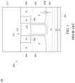
- FIG. 1 is a cross-sectional view of a semiconductor device including a comparative n-type power metal-oxide-semiconductor (MOS).
- MOS metal-oxide-semiconductor
- FIG. 2 is a schematic diagram of a charging system including the comparative power MOS shown in FIG. 1 .
- FIG. 3 is a schematic diagram illustrating a charging behavior of the charging system shown in FIG. 2 .
- FIG. 4 is a schematic diagram illustrating an over-charge protection mechanism of the charging system shown in FIG. 2 .
- FIG. 5 is a schematic diagram illustrating a discharging behavior of the charging system shown in FIG. 2 .
- FIG. 6 is a schematic diagram illustrating an over-discharge protection mechanism of the charging system shown in FIG. 2 .
- FIG. 7 is a cross-sectional diagram of a semiconductor device including a transistor, in accordance with some embodiments of the present disclosure.
- FIG. 8 is a schematic diagram of a charging system applied with the transistor shown in FIG. 7 , in accordance with some embodiments of the present disclosure.
- FIG. 9 is a schematic diagram illustrating a charging behavior of the charging system shown in FIG. 8 , in accordance with some embodiments of the present disclosure.
- FIG. 10 is a schematic diagram illustrating an over-charge protection mechanism of the charging system shown in FIG. 8 , in accordance with some embodiments of the present disclosure.
- FIG. 11 is a schematic diagram illustrating a discharging behavior of the charging system shown in FIG. 8 , in accordance with some embodiments of the present disclosure.
- FIG. 12 is a schematic diagram illustrating an over-discharge protection mechanism of the charging system shown in FIG. 8 , in accordance with some embodiments of the present disclosure.
- FIG. 13 is a schematic diagram of another charging system applied with the transistor shown in FIG. 7 , in accordance with some embodiments of the present disclosure.
- FIG. 14 is a cross-sectional diagram of a semiconductor device including another transistor, in accordance with some embodiments of the present disclosure.
- FIG. 15 is a cross-sectional diagram of a semiconductor device including still another transistor, in accordance with some embodiments of the present disclosure.
- first, second, third, etc. may be used herein to describe various elements, components, regions, layers or sections, these elements, components, regions, layers or sections are not limited by these terms. Rather, these terms are merely used to distinguish one element, component, region, layer or section from another region, layer or section. Thus, a first element, component, region, layer or section discussed below could be termed a second element, component, region, layer or section without departing from the teachings of the present inventive concept.
- FIG. 1 is a cross-sectional view of a semiconductor device 200 including a comparative power metal-oxide-semiconductor (MOS) transistor M 0 .
- the power MOS transistor M 0 includes an n-type source region 206 in a p-well region 205 in a substrate 201 of the semiconductor device 200 , an n-type drain region 203 in the substrate 201 , a gate structure 211 formed of a gate material 210 and a dielectric layer 212 , and a p-type body region 204 in the p-well region 205 .
- Dopant types of the source region 206 , the p-well region 205 and the drain region 203 define the power MOS transistor M 0 as an n-type power MOS transistor.
- a body of a power MOS transistor is required to be biased so as to control a voltage level of the body, thereby, for example, controlling a threshold voltage of the power MOS transistor.
- the body is short-circuited to a source of the power MOS transistor. For such reasons, as illustrated in FIG. 1 , the body region 204 is short-circuited to the source region 206 via a metal layer 215 of the semiconductor device 200 .
- the p-well region 205 and the drain region 203 have opposite dopant types. As such, a parasitic diode PD 0 is defined at a junction therebetween.
- the p-well region 205 and the drain region 203 serve as an anode and a cathode, respectively, of the parasitic diode PD 0 .
- the p-well region 205 and the body region 204 have the same dopant type.
- the anode of the parasitic diode PD 0 is short-circuited to the body region 204 , and further short-circuited to the source region 206 via the metal layer 215 .
- the anode and the cathode of the parasitic diode PD 0 are coupled to the source region 206 and the drain region 203 , respectively.
- the parasitic diode PD 0 provides a conduction path between the source region 206 and the drain region 203 when the parasitic diode PD 0 is conducting, which would cause failure of an over-discharge protection mechanism and an over-charge protection mechanism of a charging system applied with only one power MOS transistor M 0 , as will be described in detail with reference to FIGS. 4 and 6 .
- FIG. 2 is a schematic diagram of a charging system 10 including two comparative power MOS transistors M 0 of FIG. 1 .
- the charging system 10 includes a control device 14 and a battery 12 in addition to two power MOS transistors M 1 and M 2 .
- the power MOS transistor M 1 includes a source S 1 , a drain D 1 , and a gate G 1 .
- the power MOS transistor M 2 includes a source S 2 , a drain D 2 , and a gate G 2 .
- the parasitic diodes PD 0 are individually denoted. PD 1 and PD 2 .
- An anode and a cathode of the parasitic diode PD 1 are coupled to the source S 1 and the drain D 1 , respectively, of the power MOS transistor M 1 .
- an anode and a cathode of the parasitic diode PD 2 are coupled to the source S 2 and the drain D 2 , respectively, of the power MOS transistor M 2 .
- the drain D 1 of the power MOS transistor M 1 is coupled to the drain D 2 of the power MOS transistor M 2 . Consequently, the power MOS transistor M 1 and the power MOS transistor M 2 together form a common drain structure.
- the control device 14 functions to control conductive states of the power MOS transistors M 1 and M 2 in response to a battery voltage of the battery 12 . In some operations, the control device 14 determines the battery voltage based on a voltage level at a node 16 of the charging system 10 . In further detail, the control device 14 has two output ports 140 and 142 . The control device 14 controls the power MOS transistors M 1 and M 2 by transmitting control signals at its output ports 140 and 142 to the power MOS transistors M 1 and M 2 , respectively. An approach to controlling the power MOS transistors M 1 and M 2 will be described in detail with reference to FIGS. 3 to 6 .
- FIG. 3 is a schematic diagram illustrating a charging behavior of the charging system 10 shown in FIG. 2 .
- a charger 18 is adapted to the charging system 10 at ports V+ and V ⁇ of the charging system 10 .
- the control device 14 controls the power MOS transistors M 1 and M 2 to be conducting. As such, a closed loop is formed, and the charger 18 charges the battery 12 .
- FIG. 4 is a schematic diagram illustrating an over-charge protection mechanism of the charging system 10 shown in FIG. 2 .
- the control device 14 determines that the battery voltage exceeds a threshold voltage, which means that an undesired over-charge circumstance may occur.
- the control device 14 functions to break the closed loop by controlling the power MOS transistor M 2 to be not conducting, and, in some operations, by controlling both the power MOS transistors M 1 and M 2 to be not conducting.
- the power MOS transistor M 1 may still provide a conduction path.
- the anode and the cathode of the parasitic diode PD 1 are coupled to an anode having a relatively high voltage level and a cathode having a relatively low voltage level of the charger 18 , respectively.
- the parasitic diode PD 1 is conducting.
- the power MOS transistor M 1 provides a conduction path through the parasitic diode PD 1 .
- the power MOS transistor M 2 when the power MOS transistor M 2 is controlled to be not conducting, the power MOS transistor M 2 is actually not conducting. No conduction path is provided by the power MOS transistor M 2 .
- the anode and the cathode of the parasitic diode PD 2 are coupled to a cathode having a relatively low voltage level and an anode having a relatively high voltage level of the charger 18 , respectively. As such, the parasitic diode PD 2 is not conducting. As a result, no conduction path is provided by the parasitic diode PD 2 .
- the charger 18 stops charging the battery 12 .
- the undesired over-charge circumstance is avoided.
- the power MOS transistors M 1 and M 2 are required to complete the over-charge protection mechanism. It is assumed that the power MOS transistor M 2 is removed from the charging system 10 .
- the charging system 10 is only applied with a single power MOS transistor M 1 .
- the cathode of the parasitic diode PD 1 is accordingly coupled to the cathode (i.e., the port V ⁇ ) of the charger 18 . If the control device 14 determines that the undesired over-charge circumstance may occur and therefore the control device 14 controls the power MOS transistors M 1 to be not conducting, as previously mentioned the parasitic diode PD 1 still provides a conduction path. As such, the closed loop is not broken, and the charger 18 continues charging the battery 12 . As a result, the undesired over-charge circumstance eventually occurs.
- the control device 14 has to be configured to have two ports 140 and 142 .
- FIG. 5 is a schematic diagram illustrating a discharging behavior of the charging system 10 shown in FIG. 2 .
- a load 19 is adapted to the charging system 10 at ports V+ and V ⁇ of the charging system 10 .
- the control device 14 controls the power MOS transistors M 1 and M 2 to be conducting. As such, a closed loop is formed, and the battery 12 discharges so as to charge the load 19 .
- FIG. 6 is a schematic diagram illustrating an over-discharge protection mechanism of the charging system 10 shown in FIG. 2 .
- the control device 14 determines that the battery voltage is lower than the threshold voltage, which means that an undesired over-discharge circumstance may occur.
- the control device 14 functions to break the closed loop by controlling the power MOS transistor M 1 to be not conducting, and, in some operations, by controlling both the power MOS transistors M 1 and M 2 to be not conducting.
- the power MOS transistor M 2 may still provide a conduction path.
- the anode and the cathode of the parasitic diode PD 2 are coupled to an anode having a relatively high voltage level and a cathode having a relatively low voltage level of the battery 12 , respectively.
- the parasitic diode PD 2 is conducting.
- the power MOS transistor M 2 provides a conduction path through the parasitic diode PD 2 .
- the power MOS transistor M 1 when the power MOS transistor M 1 is controlled to be not conducting, the power MOS transistor M 1 is actually not conducting. No conduction path is provided.
- the anode and the cathode of the parasitic diode PD 1 are coupled to the cathode having a relatively low voltage level and the anode having a relatively high voltage level of the battery 12 , respectively. As such, the parasitic diode PD 1 is not conducting. As a result, no conduction path is provided.
- the power MOS transistors M 1 and M 2 are required to complete the over-discharge protection mechanism. It is assumed that the power MOS transistor M 1 is removed from the charging system 10 .
- the charging system 10 is applied with a single power MOS transistor M 2 .
- the cathode of the parasitic diode PD 2 is accordingly coupled to the cathode of the battery 12 . If the control device 14 determines that the undesired over-discharge circumstance may occur and therefore controls the power MOS transistor M 2 to be not conducting, as previously mentioned the parasitic diode PD 2 still provides a conduction path. As such, the closed loop is not broken, and the battery 12 continues discharging. As a result, the undesired over-discharge circumstance eventually occurs.
- FIG. 7 is a cross-sectional diagram of a semiconductor device 30 including a transistor 32 , in accordance with some embodiments of the present disclosure.
- the transistor 32 includes a first source/drain S/D) region 306 defined in a first well 304 in a substrate 300 of the semiconductor device 30 , a second S/D region 310 defined in a second well 308 in the substrate 300 , and a gate structure 33 formed of a dielectric layer 312 and a conductive material 314 .
- Definitions of regions, wells and other components of the present disclosure can be found in U.S. Utility patent application Ser. No. 13/740,898, filed on Jan. 14, 2013 and entitled “POWER MOSFET DEVICE WITH A GATE CONDUCTOR SURROUNDING SOURCE AND DRAIN PILLARS.” This application is incorporated herein by reference.
- the first S/D region 306 is an n-type region; the first well 304 is a p-type well; a double diffusion layer 302 is an n-type layer in the substrate 300 ; the second well 308 is an n-type well; and the second S/D region 310 is an n-type region.
- a dopant type of wells and regions of the semiconductor device 30 is opposite to that of aforesaid embodiment.
- the semiconductor device 30 is asymmetrical in dopant type with respect to the gate structure 33 .
- each of the regions and wells in the semiconductor device 30 has an n-type dopant except for the first well 304 having a p-type dopant.
- the gate structure 33 is disposed in a trench of the substrate 300 . Consequently, the transistor 32 includes a trench gate structure. Moreover, the gate structure 33 is between the first S/D region 306 and the second S/D region 310 . Furthermore, the first S/D region 306 is immediately adjacent to the gate structure 33 , which is in turn immediately adjacent to the second S/D region 310 .
- the first S/D region 306 is at one side of the gate structure 33 , and disposed over the double diffusion layer 302 in the substrate 300 of the semiconductor device 30 , wherein the double diffusion layer 302 is beneath the first well 304 .
- the first S/D region 306 is entirely defined in a portion of the first well 304 in proximity to a top surface 37 of the substrate 300 .
- the first S/D region. 306 is n-type heavily doped.
- the doping concentration in an upper portion of the double diffusion layer 302 is higher than the doping concentration in a lower portion of the double diffusion layer 302 .
- the second S/D region 310 is at the other side of the gate structure 33 , and disposed over the double diffusion layer 302 , wherein the double diffusion layer 302 is beneath the second well 308 . Additionally, the second S/D region 310 is level with the first S/D region 306 . Furthermore, the second S/D region 310 has the same dopant type as the second well 308 and the double diffusion layer 302 . As such, the second S/D region 310 , the second well 308 and the double diffusion layer 302 can be deemed as together serving as the second S/D region of the transistor 32 .
- the transistor 32 is free of a body region in the first well 304 . Consequently, there is no need to provide a conductive layer, like the metal layer 215 shown in FIG. 1 , to connect a nonexistent body region to the first S/D region 306 or the second S/D region 310 so as to bias the nonexistent body region.
- the first well 304 and the double diffusion layer 302 have opposite dopant types. As such, a diode PD 3 is defined at a junction therebetween.
- the first well 304 and the double diffusion layer 302 serve as an anode and a cathode, respectively, of the diode PD 3 .
- the anode of the diode PD 3 is not short-circuited to the first S/D region 306 , which means that the anode of the diode PD 3 and the first S/D region 306 from an open circuit.
- the diode PD 3 does not provide a conduction path between the double diffusion layer 302 and the first S/D region 306 , or between the second S/D region 310 and the first S/D region 306 .
- an over-charge protection mechanism and an over-discharge protection mechanism of the charging system still function normally, as will be described in detail with reference to FIGS. 9 to 12 .
- a semiconductor manufacturing process is relatively simple.
- the second well 308 is an n-type well.
- the transistor 32 includes one channel controllable by the gate structure 33 .
- the present disclosure is not limited thereto.
- the second well 308 is a p-type well.
- the transistor 32 includes two channels controllable by the gate structure 33 .
- FIG. 8 is a schematic diagram of a charging system 40 applied with one transistor 32 shown in FIG. 7 , in accordance with some embodiments of the present disclosure.
- the charging system 40 is similar to the charging system 10 described and illustrated with reference to FIG. 2 except that, for example, the charging system 40 includes a logic AND gate 42 , in addition to the transistor 32 .
- the first S/D region 306 is called the first S/D 306 ; and the second S/D region 310 is called the second S/D 310 .
- the control device 14 functions to control conducting states of the transistor 32 in response to a battery voltage of the battery 12 to activate an over-charge protection mechanism and an over-discharge protection mechanism, as will be described in detail with reference to FIGS. 9 to 12 . Since the control device 14 has two output ports 140 and 142 , two control signals from the two output ports 140 and 142 are converted into a single control signal by the logic AND gate 42 .
- control device 14 functions to activate an over-current protection mechanism based on a voltage level at the second S/D 310 of the transistor 32 .
- FIG. 9 is a schematic diagram illustrating a charging behavior of the charging system 40 shown in FIG. 8 , in accordance with some embodiments of the present disclosure.
- a charger 18 is adapted to the charging system 40 at ports V+ and V ⁇ of the charging system 40 .
- the control device 14 controls the transistor 32 to be conducting. As such, a closed loop is formed, and the charger 18 charges the battery 12 .
- FIG. 10 is a schematic diagram illustrating an over-charge protection mechanism of the charging system 40 shown in FIG. 8 , in accordance with some embodiments of the present disclosure.
- the control device 14 determines that the battery voltage achieves a threshold voltage, which means that an undesired over-charge circumstance may occur.
- the control device 14 functions to break the closed loop by controlling the transistor 32 to be not conducting.
- the parasitic diode PD 3 provides no conduction path between the first S/D 306 and the second S/D 310 of the transistor 32 , when the transistor 32 is controlled to be not conducting, the transistor 32 is actually not conducting, unlike the power MOS transistors M 1 and M 2 . Since the closed loop is broken, the charger 18 stops charging the battery 12 . The undesired over-charge circumstance is avoided. In the charging system 40 , only one transistor, the transistor 32 , is required to complete the over-charge protection mechanism.
- FIG. 11 is a schematic diagram illustrating a discharging behavior of the charging system 40 shown in FIG. 8 , in accordance with some embodiments of the present disclosure.
- a load 19 is adapted to the charging system 40 at ports V+ and V ⁇ of the charging system 40 for receiving electrical energy from the battery 12 .
- the battery 12 discharges.
- the control device 14 controls the transistor 32 to be conducting. As such, a closed loop is formed, and the battery 12 discharges to charge the load 19 .
- FIG. 12 is a schematic diagram illustrating an over-discharge protection mechanism of the charging system 40 shown in FIG. 8 , in accordance with some embodiments of the present disclosure.
- the control device 14 determines that the battery voltage achieves another threshold voltage, which means that an undesired over-discharge circumstance may occur.
- the control device 14 functions to break the closed loop by controlling the transistor 32 to be not conducting.
- the diode PD 3 provides no conduction path between the first S/D 306 and the second S/D 310 of the transistor 32 , when the transistor 32 is controlled to be not conducting, the transistor 32 is actually not conducting, unlike the power MOS transistors M 1 and M 2 . Since the closed loop is broken, the battery 12 stops discharging. The undesired over-discharge circumstance is avoided. In the charging system 40 , only one transistor, the transistor 32 , is required to complete the over-discharge protection mechanism.
- FIG. 13 is a schematic diagram of another charging system 50 applied with the transistor 32 shown in FIG. 7 , in accordance with some embodiments of the present disclosure.
- the charging system 50 is similar to the charging system 40 described and illustrated with reference to FIG. 8 except that, for example, the charging system 50 includes a control device 54 with one output port 540 .
- the control device 54 controls the conducting state of the transistor 32 via, the one output port 540 .
- FIG. 14 is a cross-sectional diagram of a semiconductor device 60 including another transistor 62 , in accordance with some embodiments of the present disclosure.
- the transistor 62 is similar to the transistor 32 described and illustrated with reference to FIG. 7 except that, for example, the transistor 62 includes a double diffusion layer 602 .
- a side surface 604 of the double diffusion layer 602 is aligned with a sidewall 316 of the gate structure 33 .
- a parasitic diode PD 4 analogous to the parasitic diode PD 3 described and illustrated with reference to FIG. 7 , is defined by the substrate 300 and the double diffusion layer 602 .
- the transistor 62 can also be applied to the charging system 40 , and provides the same benefits as the transistor 32 .
- FIG. 15 is a cross-sectional diagram of a semiconductor device 70 including still another transistor 72 , in accordance with some embodiments of the present disclosure.
- the transistor 72 is similar to the transistor 62 described and illustrated with reference to FIG. 14 except that, for example, the transistor 72 includes a second S/D region 610 and is free of the second well 308 described in the embodiment of FIG. 14 .
- the second S/D region 610 extends from a top surface 37 of the substrate 300 to the double diffusion layer 602 , and is in contact with the double diffusion layer 602 .
- the transistor 72 can also be applied to the charging system 40 , and provides the same benefits as the transistor 32 .
- the transistor 32 is free of a body region in the first well 304 . Consequently, there is no need to provide a conductive layer, like the metal layer 215 shown in FIG. 1 , to connect the nonexistent body region to the first S/D region 306 or the second S/D region 310 so as to bias the nonexistent body region.
- the diode PD 3 is defined at a junction between the first well 304 and the double diffusion layer 302 , in the absence of the body region and the conductive layer, the anode of the diode PD 3 is not short-circuited to the first S/D region 306 . As such, the diode PD 3 does not provide a conduction path between the double diffusion layer 302 and the first S/D region 306 , or between the second S/D region 310 and the first S/D region 306 . As a result, even though a charging system only adopts one transistor 32 , an over-charge protection mechanism and an over-discharge protection mechanism of the charging system still function normally. Moreover, because no body region is required, a semiconductor manufacturing process is relatively simple.
- the semiconductor device includes a transistor.
- the transistor includes a first source/drain (S/D) region, a second S/D region and a gate structure.
- the first S/D region is defined in a first well on a double diffusion layer, wherein the first well and the double diffusion layer define a diode at a junction therebetween, wherein an anode of the diode and the first S/D region forms an open circuit therebetween.
- the gate structure is between the first S/D region and the second S/D region.
- the semiconductor device includes a transistor.
- the transistor includes a first source/drain (S/D) region, a second S/D region and a gate structure.
- the first S/D region in a first well on a double diffusion layer.
- the first well and the double diffusion layer are defined in a substrate.
- the first well has a dopant type opposite to that of the double diffusion layer.
- the first S/D region is entirely defined in a portion of the first well in proximity to a top surface of the substrate.
- the gate structure is between the first S/D region and the second S/D region.
- the charging system includes the transistor; a battery; and a control device configured to, in response to a battery voltage of the battery, control a conductive state of the transistor.
Landscapes
- Engineering & Computer Science (AREA)
- Power Engineering (AREA)
- Charge And Discharge Circuits For Batteries Or The Like (AREA)
- Metal-Oxide And Bipolar Metal-Oxide Semiconductor Integrated Circuits (AREA)
Abstract
Description
Claims (18)
Priority Applications (6)
| Application Number | Priority Date | Filing Date | Title |
|---|---|---|---|
| US15/858,746 US11227925B2 (en) | 2017-04-14 | 2017-12-29 | Semiconductor device and charging system using the same |
| TW109104557A TWI731583B (en) | 2017-04-14 | 2018-02-01 | Semiconductor device and charging system using the same |
| TW107103600A TWI689102B (en) | 2017-04-14 | 2018-02-01 | Semiconductor device and charging system using the same |
| JP2018040518A JP2018182307A (en) | 2017-04-14 | 2018-03-07 | Semiconductor device and charging system thereof |
| CN201810224530.2A CN108735815A (en) | 2017-04-14 | 2018-03-19 | Semiconductor device and charging system thereof |
| JP2020065972A JP6949167B2 (en) | 2017-04-14 | 2020-04-01 | Semiconductor devices and their charging systems |
Applications Claiming Priority (2)
| Application Number | Priority Date | Filing Date | Title |
|---|---|---|---|
| US201762485709P | 2017-04-14 | 2017-04-14 | |
| US15/858,746 US11227925B2 (en) | 2017-04-14 | 2017-12-29 | Semiconductor device and charging system using the same |
Publications (2)
| Publication Number | Publication Date |
|---|---|
| US20180301554A1 US20180301554A1 (en) | 2018-10-18 |
| US11227925B2 true US11227925B2 (en) | 2022-01-18 |
Family
ID=63790317
Family Applications (1)
| Application Number | Title | Priority Date | Filing Date |
|---|---|---|---|
| US15/858,746 Active 2039-06-18 US11227925B2 (en) | 2017-04-14 | 2017-12-29 | Semiconductor device and charging system using the same |
Country Status (4)
| Country | Link |
|---|---|
| US (1) | US11227925B2 (en) |
| JP (2) | JP2018182307A (en) |
| CN (1) | CN108735815A (en) |
| TW (2) | TWI689102B (en) |
Cited By (1)
| Publication number | Priority date | Publication date | Assignee | Title |
|---|---|---|---|---|
| US20230317841A1 (en) * | 2021-03-29 | 2023-10-05 | Nuvoton Technology Corporation Japan | Semiconductor device, battery protection circuit, and power management circuit |
Families Citing this family (1)
| Publication number | Priority date | Publication date | Assignee | Title |
|---|---|---|---|---|
| CN112289792A (en) * | 2020-09-14 | 2021-01-29 | 珠海迈巨微电子有限责任公司 | Semiconductor Devices for Battery Protection |
Citations (11)
| Publication number | Priority date | Publication date | Assignee | Title |
|---|---|---|---|---|
| JPS60154671A (en) | 1984-01-25 | 1985-08-14 | Hitachi Ltd | Semiconductor device |
| JPH0335534A (en) | 1989-07-03 | 1991-02-15 | Seiko Epson Corp | Manufacturing method of semiconductor device |
| JPH0697450B2 (en) | 1987-10-30 | 1994-11-30 | インターナシヨナル・ビジネス・マシーンズ・コーポレーシヨン | Computer system |
| US5640034A (en) * | 1992-05-18 | 1997-06-17 | Texas Instruments Incorporated | Top-drain trench based resurf DMOS transistor structure |
| CN1327288A (en) | 2000-06-02 | 2001-12-19 | 精工电子有限公司 | Charging/discharging type power source |
| US6351009B1 (en) * | 1999-03-01 | 2002-02-26 | Fairchild Semiconductor Corporation | MOS-gated device having a buried gate and process for forming same |
| TW495951B (en) | 2001-05-29 | 2002-07-21 | Taiwan Semiconductor Mfg | Electro-static discharge protection design for charged-device mode using deep well structure |
| CN101364610A (en) | 2007-08-10 | 2009-02-11 | 力芯科技股份有限公司 | Trench type power metal oxide semiconductor transistor and manufacturing method thereof |
| JP2013004539A (en) | 2011-06-10 | 2013-01-07 | Toshiba Corp | Semiconductor device, metal film manufacturing method, and semiconductor device manufacturing method |
| JP2014049481A (en) | 2012-08-29 | 2014-03-17 | Toshiba Corp | Semiconductor device |
| US20200203353A1 (en) * | 2017-09-06 | 2020-06-25 | Changxin Memory Technologies, Inc. | Semiconductor memory device structure |
Family Cites Families (10)
| Publication number | Priority date | Publication date | Assignee | Title |
|---|---|---|---|---|
| GB9820904D0 (en) * | 1998-09-26 | 1998-11-18 | Koninkl Philips Electronics Nv | Bi-directional semiconductor switch and switch circuit for battery-powered equipment |
| JP5321657B2 (en) * | 2003-02-17 | 2013-10-23 | 富士電機株式会社 | Bidirectional element and semiconductor device |
| EP1498998A1 (en) * | 2003-07-16 | 2005-01-19 | Dialog Semiconductor GmbH | Protection switch with reverse voltage protection |
| JP4984398B2 (en) * | 2005-02-04 | 2012-07-25 | 富士電機株式会社 | Semiconductor device and manufacturing method thereof |
| JP4248548B2 (en) * | 2005-03-30 | 2009-04-02 | パナソニック株式会社 | High breakdown voltage semiconductor device and manufacturing method thereof |
| KR101710599B1 (en) * | 2011-01-12 | 2017-02-27 | 삼성전자 주식회사 | Semiconductor device and fabricating method thereof |
| JP5927017B2 (en) * | 2012-04-20 | 2016-05-25 | ルネサスエレクトロニクス株式会社 | Semiconductor device and manufacturing method of semiconductor device |
| US8723238B1 (en) * | 2013-03-15 | 2014-05-13 | Semiconductor Components Industries, Llc | Method of forming a transistor and structure therefor |
| WO2015166654A1 (en) * | 2014-05-01 | 2015-11-05 | パナソニックIpマネジメント株式会社 | Semiconductor device and semiconductor module |
| TWI560886B (en) * | 2014-09-25 | 2016-12-01 | Inotera Memories Inc | Non-floating vertical transistor structure and method for forming the same |
-
2017
- 2017-12-29 US US15/858,746 patent/US11227925B2/en active Active
-
2018
- 2018-02-01 TW TW107103600A patent/TWI689102B/en active
- 2018-02-01 TW TW109104557A patent/TWI731583B/en active
- 2018-03-07 JP JP2018040518A patent/JP2018182307A/en active Pending
- 2018-03-19 CN CN201810224530.2A patent/CN108735815A/en active Pending
-
2020
- 2020-04-01 JP JP2020065972A patent/JP6949167B2/en active Active
Patent Citations (13)
| Publication number | Priority date | Publication date | Assignee | Title |
|---|---|---|---|---|
| JPS60154671A (en) | 1984-01-25 | 1985-08-14 | Hitachi Ltd | Semiconductor device |
| JPH0697450B2 (en) | 1987-10-30 | 1994-11-30 | インターナシヨナル・ビジネス・マシーンズ・コーポレーシヨン | Computer system |
| JPH0335534A (en) | 1989-07-03 | 1991-02-15 | Seiko Epson Corp | Manufacturing method of semiconductor device |
| US5640034A (en) * | 1992-05-18 | 1997-06-17 | Texas Instruments Incorporated | Top-drain trench based resurf DMOS transistor structure |
| US6351009B1 (en) * | 1999-03-01 | 2002-02-26 | Fairchild Semiconductor Corporation | MOS-gated device having a buried gate and process for forming same |
| JP2001352683A (en) | 2000-06-02 | 2001-12-21 | Seiko Instruments Inc | Charge / discharge type power supply |
| CN1327288A (en) | 2000-06-02 | 2001-12-19 | 精工电子有限公司 | Charging/discharging type power source |
| US6690559B2 (en) | 2000-06-02 | 2004-02-10 | Seiko Instruments Inc. | Charge/discharge type power supply |
| TW495951B (en) | 2001-05-29 | 2002-07-21 | Taiwan Semiconductor Mfg | Electro-static discharge protection design for charged-device mode using deep well structure |
| CN101364610A (en) | 2007-08-10 | 2009-02-11 | 力芯科技股份有限公司 | Trench type power metal oxide semiconductor transistor and manufacturing method thereof |
| JP2013004539A (en) | 2011-06-10 | 2013-01-07 | Toshiba Corp | Semiconductor device, metal film manufacturing method, and semiconductor device manufacturing method |
| JP2014049481A (en) | 2012-08-29 | 2014-03-17 | Toshiba Corp | Semiconductor device |
| US20200203353A1 (en) * | 2017-09-06 | 2020-06-25 | Changxin Memory Technologies, Inc. | Semiconductor memory device structure |
Non-Patent Citations (2)
| Title |
|---|
| Office Action and Cited References dated Jun. 9, 2021 issued by the Japanese Patent Office for counterpart application No. 2020-065972 (provided with brief translation). |
| Office Action issued in corresponding CN application No. 201810224530.2 dated Nov. 2, 2020. |
Cited By (2)
| Publication number | Priority date | Publication date | Assignee | Title |
|---|---|---|---|---|
| US20230317841A1 (en) * | 2021-03-29 | 2023-10-05 | Nuvoton Technology Corporation Japan | Semiconductor device, battery protection circuit, and power management circuit |
| US11894456B2 (en) * | 2021-03-29 | 2024-02-06 | Nuvoton Technology Corporation Japan | Semiconductor device, battery protection circuit, and power management circuit |
Also Published As
| Publication number | Publication date |
|---|---|
| US20180301554A1 (en) | 2018-10-18 |
| JP6949167B2 (en) | 2021-10-13 |
| CN108735815A (en) | 2018-11-02 |
| TWI689102B (en) | 2020-03-21 |
| TW202025496A (en) | 2020-07-01 |
| TWI731583B (en) | 2021-06-21 |
| TW201838191A (en) | 2018-10-16 |
| JP2018182307A (en) | 2018-11-15 |
| JP2020113788A (en) | 2020-07-27 |
Similar Documents
| Publication | Publication Date | Title |
|---|---|---|
| US9111764B2 (en) | Integrated semiconductor device and a bridge circuit with the integrated semiconductor device | |
| US10164079B2 (en) | Power semiconductor device | |
| JP6618960B2 (en) | N-channel bipolar power semiconductor device having p-layer in drift space | |
| US9818827B2 (en) | Field plate trench semiconductor device with planar gate | |
| US8901661B2 (en) | Semiconductor device with first and second field-effect structures and an integrated circuit including the semiconductor device | |
| US12328901B2 (en) | Bidirectional conduction trench gate power MOS device and manufacturing method thereof | |
| US10600862B2 (en) | High voltage termination structure of a power semiconductor device | |
| US10910487B2 (en) | Power semiconductor device having trench electrodes biased at three different electrical potentials, and method of manufacturing the same | |
| US11848354B2 (en) | Diode structure of a power semiconductor device | |
| US11227949B2 (en) | Power semiconductor devices with low specific on-resistance | |
| US11227925B2 (en) | Semiconductor device and charging system using the same | |
| US9064953B2 (en) | Semiconductor device including a drift zone and a drift control zone | |
| CN110534575A (en) | A kind of VDMOS device | |
| US9484410B2 (en) | Lateral MOS power transistor having front side drain electrode and back side source electrode | |
| US20230147486A1 (en) | Integrated freewheeling diode and extraction device | |
| US10868159B2 (en) | Power semiconductor device | |
| US20250374655A1 (en) | Dual Gate Power Semiconductor Device and Method of Controlling a Dual Gate Power Semiconductor Device |
Legal Events
| Date | Code | Title | Description |
|---|---|---|---|
| FEPP | Fee payment procedure |
Free format text: ENTITY STATUS SET TO UNDISCOUNTED (ORIGINAL EVENT CODE: BIG.); ENTITY STATUS OF PATENT OWNER: SMALL ENTITY |
|
| AS | Assignment |
Owner name: PTEK TECHNOLOGY CO., LTD., TAIWAN Free format text: ASSIGNMENT OF ASSIGNORS INTEREST;ASSIGNORS:TANG, MING;CHIAO, SHIH PING;REEL/FRAME:044631/0304 Effective date: 20171219 |
|
| FEPP | Fee payment procedure |
Free format text: ENTITY STATUS SET TO SMALL (ORIGINAL EVENT CODE: SMAL); ENTITY STATUS OF PATENT OWNER: SMALL ENTITY |
|
| STPP | Information on status: patent application and granting procedure in general |
Free format text: DOCKETED NEW CASE - READY FOR EXAMINATION |
|
| STPP | Information on status: patent application and granting procedure in general |
Free format text: NON FINAL ACTION MAILED |
|
| STPP | Information on status: patent application and granting procedure in general |
Free format text: RESPONSE TO NON-FINAL OFFICE ACTION ENTERED AND FORWARDED TO EXAMINER |
|
| STPP | Information on status: patent application and granting procedure in general |
Free format text: NON FINAL ACTION MAILED |
|
| STPP | Information on status: patent application and granting procedure in general |
Free format text: ADVISORY ACTION MAILED |
|
| STPP | Information on status: patent application and granting procedure in general |
Free format text: DOCKETED NEW CASE - READY FOR EXAMINATION |
|
| STPP | Information on status: patent application and granting procedure in general |
Free format text: NOTICE OF ALLOWANCE MAILED -- APPLICATION RECEIVED IN OFFICE OF PUBLICATIONS |
|
| STPP | Information on status: patent application and granting procedure in general |
Free format text: PUBLICATIONS -- ISSUE FEE PAYMENT VERIFIED |
|
| STPP | Information on status: patent application and granting procedure in general |
Free format text: PUBLICATIONS -- ISSUE FEE PAYMENT VERIFIED Free format text: AWAITING TC RESP, ISSUE FEE PAYMENT VERIFIED |
|
| STCF | Information on status: patent grant |
Free format text: PATENTED CASE |
|
| MAFP | Maintenance fee payment |
Free format text: PAYMENT OF MAINTENANCE FEE, 4TH YR, SMALL ENTITY (ORIGINAL EVENT CODE: M2551); ENTITY STATUS OF PATENT OWNER: SMALL ENTITY Year of fee payment: 4 |