US11227649B2 - Apparatuses and methods for staggered timing of targeted refresh operations - Google Patents
Apparatuses and methods for staggered timing of targeted refresh operations Download PDFInfo
- Publication number
- US11227649B2 US11227649B2 US16/375,716 US201916375716A US11227649B2 US 11227649 B2 US11227649 B2 US 11227649B2 US 201916375716 A US201916375716 A US 201916375716A US 11227649 B2 US11227649 B2 US 11227649B2
- Authority
- US
- United States
- Prior art keywords
- refresh
- type
- address
- refresh operation
- memory
- Prior art date
- Legal status (The legal status is an assumption and is not a legal conclusion. Google has not performed a legal analysis and makes no representation as to the accuracy of the status listed.)
- Active
Links
Images


Classifications
-
- G—PHYSICS
- G11—INFORMATION STORAGE
- G11C—STATIC STORES
- G11C11/00—Digital stores characterised by the use of particular electric or magnetic storage elements; Storage elements therefor
- G11C11/21—Digital stores characterised by the use of particular electric or magnetic storage elements; Storage elements therefor using electric elements
- G11C11/34—Digital stores characterised by the use of particular electric or magnetic storage elements; Storage elements therefor using electric elements using semiconductor devices
- G11C11/40—Digital stores characterised by the use of particular electric or magnetic storage elements; Storage elements therefor using electric elements using semiconductor devices using transistors
- G11C11/401—Digital stores characterised by the use of particular electric or magnetic storage elements; Storage elements therefor using electric elements using semiconductor devices using transistors forming cells needing refreshing or charge regeneration, i.e. dynamic cells
- G11C11/406—Management or control of the refreshing or charge-regeneration cycles
- G11C11/40611—External triggering or timing of internal or partially internal refresh operations, e.g. auto-refresh or CAS-before-RAS triggered refresh
-
- G—PHYSICS
- G11—INFORMATION STORAGE
- G11C—STATIC STORES
- G11C11/00—Digital stores characterised by the use of particular electric or magnetic storage elements; Storage elements therefor
- G11C11/21—Digital stores characterised by the use of particular electric or magnetic storage elements; Storage elements therefor using electric elements
- G11C11/34—Digital stores characterised by the use of particular electric or magnetic storage elements; Storage elements therefor using electric elements using semiconductor devices
- G11C11/40—Digital stores characterised by the use of particular electric or magnetic storage elements; Storage elements therefor using electric elements using semiconductor devices using transistors
- G11C11/401—Digital stores characterised by the use of particular electric or magnetic storage elements; Storage elements therefor using electric elements using semiconductor devices using transistors forming cells needing refreshing or charge regeneration, i.e. dynamic cells
- G11C11/406—Management or control of the refreshing or charge-regeneration cycles
- G11C11/40615—Internal triggering or timing of refresh, e.g. hidden refresh, self refresh, pseudo-SRAMs
-
- G—PHYSICS
- G11—INFORMATION STORAGE
- G11C—STATIC STORES
- G11C11/00—Digital stores characterised by the use of particular electric or magnetic storage elements; Storage elements therefor
- G11C11/21—Digital stores characterised by the use of particular electric or magnetic storage elements; Storage elements therefor using electric elements
- G11C11/34—Digital stores characterised by the use of particular electric or magnetic storage elements; Storage elements therefor using electric elements using semiconductor devices
- G11C11/40—Digital stores characterised by the use of particular electric or magnetic storage elements; Storage elements therefor using electric elements using semiconductor devices using transistors
- G11C11/401—Digital stores characterised by the use of particular electric or magnetic storage elements; Storage elements therefor using electric elements using semiconductor devices using transistors forming cells needing refreshing or charge regeneration, i.e. dynamic cells
- G11C11/406—Management or control of the refreshing or charge-regeneration cycles
- G11C11/40618—Refresh operations over multiple banks or interleaving
-
- G—PHYSICS
- G11—INFORMATION STORAGE
- G11C—STATIC STORES
- G11C11/00—Digital stores characterised by the use of particular electric or magnetic storage elements; Storage elements therefor
- G11C11/21—Digital stores characterised by the use of particular electric or magnetic storage elements; Storage elements therefor using electric elements
- G11C11/34—Digital stores characterised by the use of particular electric or magnetic storage elements; Storage elements therefor using electric elements using semiconductor devices
- G11C11/40—Digital stores characterised by the use of particular electric or magnetic storage elements; Storage elements therefor using electric elements using semiconductor devices using transistors
- G11C11/401—Digital stores characterised by the use of particular electric or magnetic storage elements; Storage elements therefor using electric elements using semiconductor devices using transistors forming cells needing refreshing or charge regeneration, i.e. dynamic cells
- G11C11/4063—Auxiliary circuits, e.g. for addressing, decoding, driving, writing, sensing or timing
- G11C11/407—Auxiliary circuits, e.g. for addressing, decoding, driving, writing, sensing or timing for memory cells of the field-effect type
- G11C11/408—Address circuits
- G11C11/4085—Word line control circuits, e.g. word line drivers, - boosters, - pull-up, - pull-down, - precharge
-
- G—PHYSICS
- G11—INFORMATION STORAGE
- G11C—STATIC STORES
- G11C8/00—Arrangements for selecting an address in a digital store
- G11C8/06—Address interface arrangements, e.g. address buffers
-
- G—PHYSICS
- G11—INFORMATION STORAGE
- G11C—STATIC STORES
- G11C8/00—Arrangements for selecting an address in a digital store
- G11C8/12—Group selection circuits, e.g. for memory block selection, chip selection, array selection
-
- G—PHYSICS
- G11—INFORMATION STORAGE
- G11C—STATIC STORES
- G11C11/00—Digital stores characterised by the use of particular electric or magnetic storage elements; Storage elements therefor
- G11C11/21—Digital stores characterised by the use of particular electric or magnetic storage elements; Storage elements therefor using electric elements
- G11C11/34—Digital stores characterised by the use of particular electric or magnetic storage elements; Storage elements therefor using electric elements using semiconductor devices
- G11C11/40—Digital stores characterised by the use of particular electric or magnetic storage elements; Storage elements therefor using electric elements using semiconductor devices using transistors
- G11C11/401—Digital stores characterised by the use of particular electric or magnetic storage elements; Storage elements therefor using electric elements using semiconductor devices using transistors forming cells needing refreshing or charge regeneration, i.e. dynamic cells
- G11C11/406—Management or control of the refreshing or charge-regeneration cycles
- G11C11/40622—Partial refresh of memory arrays
Definitions
- Information may be stored on individual memory cells of the memory as a physical signal (e.g., a charge on a capacitive element).
- the memory may be a volatile memory, and the physical signal may decay over time (which may degrade or destroy the information stored in the memory cells). It may be necessary to periodically refresh the information in the memory cells by, for example, rewriting the information to restore the physical signal to an initial value.
- An auto-refresh operation may be carried out where a sequence of memory cells are periodically refreshed. Repeated access to a particular memory cell or group of memory cells (often referred to as a ‘row hammer’) may cause an increased rate of data degradation in nearby memory cells. It may be desirable to identify and refresh memory cells affected by the row hammer in a targeted refresh operation in addition to the auto-refresh operation. The targeted refresh operations may occur with timing interspersed between the auto-refresh operations.
- FIG. 1 is a block diagram of a semiconductor device according to an embodiment of the present disclosure.
- FIG. 2 is a block diagram of a memory array according to an embodiment of the present disclosure.
- FIG. 3 is a timing diagram of refresh operations in a memory device according to an embodiment of the present disclosure.
- FIG. 4 is a block diagram of a refresh control circuit according to an embodiment of the present disclosure.
- FIG. 5 is a block diagram of a row decoder according to an embodiment of the present disclosure.
- a memory device may include a plurality of memory cells.
- the memory cells may store information (e.g., as one or more bits), and may be organized at the intersection of word lines (rows) and bit lines (columns).
- a number of word lines and bit lines may be organized into a memory bank.
- a memory device may include a number of different memory banks.
- the memory device may receive one or more command signals which may indicate operations in one or more of the banks of one or more memory packages.
- the memory device may enter a refresh mode, in which wordlines in one or more of the memory banks are refreshed.
- Information in the memory cells may decay over time.
- the memory cells may be refreshed on a row-by-row basis to preserve information in the memory cells.
- the information in one or more rows may be rewritten back to the respective rows to restore an initial value of the information.
- a refresh signal may control a timing of the refresh operations.
- the memory banks may be capable of performing more than one type of refresh operation.
- a first type of refresh operation may simultaneously refresh less rows than the second type of refresh operation. Accordingly, the first type of refresh operation may draw more power than the second type. It may be important to control the amount of power used during refresh operations and reduce the peak amount of power which is drawn.
- the present disclosure is drawn to apparatuses, systems, and methods for staggering timing of refresh operations.
- the memory banks of a device may perform one or more refresh operations synchronized by the activations of the refresh signal.
- Each memory bank may receive a refresh address which indicates one or more wordlines of the bank, and may then refresh those wordlines.
- Some of the memory banks may receive refresh addresses which indicate the second type of refresh operation at different times from each other. In this manner, some of the banks may perform the first type of refresh operations simultaneous to one or more of the banks performing the second type of refresh operation. This may reduce a peak power drawn during the refresh operations on the memory device.
- FIG. 1 is a block diagram of a semiconductor device according to at least one embodiment of the disclosure.
- the semiconductor device 100 may be a semiconductor memory device, such as a DRAM device integrated on a single semiconductor chip.
- the semiconductor device 100 includes a memory array 112 .
- the memory array 112 may include of a plurality of memory banks.
- Each memory bank includes a plurality of word lines WL, a plurality of bit lines BL and /BL, and a plurality of memory cells MC arranged at intersections of the plurality of word lines WL and the plurality of bit lines BL and /BL.
- the selection of the word line WL is performed by a row control 108 and the selection of the bit lines BL and /BL is performed by a column control 110 .
- the bit lines BL and /BL are coupled to a respective sense amplifier (SAMP) 117 .
- Read data from the bit line BL or /BL is amplified by the sense amplifier SAMP 117 , and transferred to read/write amplifiers 120 over complementary local data lines (LIOT/B), transfer gate (TG) 118 , and complementary main data lines (MIO).
- write data outputted from the read/write amplifiers 120 is transferred to the sense amplifier 117 over the complementary main data lines MIO, the transfer gate 118 , and the complementary local data lines LIOT/B, and written in the memory cell MC coupled to the bit line BL or /BL.
- the semiconductor device 100 may employ a plurality of external terminals that include command and address (C/A) terminals coupled to a command and address bus to receive commands and addresses, clock terminals to receive clocks CK and /CK, data terminals DQ to provide data, and power supply terminals to receive power supply potentials VDD, VSS, VDDQ, and VSSQ.
- C/A command and address
- clock terminals to receive clocks CK and /CK
- data terminals DQ to provide data
- power supply terminals to receive power supply potentials VDD, VSS, VDDQ, and VSSQ.
- the clock terminals are supplied with external clocks CK and /CK that are provided to a clock input circuit 122 .
- the external clocks may be complementary.
- the clock input circuit 122 generates an internal clock ICLK based on the CK and /CK clocks.
- the ICLK clock is provided to the command control 106 and to an internal clock generator 124 .
- the internal clock generator 124 provides various internal clocks LCLK based on the ICLK clock.
- the LCLK clocks may be used for timing operation of various internal circuits.
- the internal data clocks LCLK are provided to the input/output circuit 126 to time operation of circuits included in the input/output circuit 126 , for example, to data receivers to time the receipt of write data.
- the C/A terminals may be supplied with memory addresses.
- the memory addresses supplied to the C/A terminals are transferred, via a command/address input circuit 102 , to an address decoder 104 .
- the address decoder 104 receives the address and supplies a decoded row address XADD to the row control 108 and supplies a decoded column address YADD to the column control 110 .
- the address decoder 104 may also supply a decoded bank address BADD, which may indicate the bank of the memory array 118 containing the decoded row address XADD and column address YADD.
- the C/A terminals may be supplied with commands.
- commands include timing commands for controlling the timing of various operations, access commands for accessing the memory, such as read commands for performing read operations and write commands for performing write operations, as well as other commands and operations.
- the access commands may be associated with one or more row address XADD, column address YADD, and bank address BADD to indicate the memory cell(s) to be accessed.
- the commands may be provided as internal command signals to a command control 106 via the command/address input circuit 102 .
- the command control 106 includes circuits to decode the internal command signals to generate various internal signals and commands for performing operations. For example, the command control 106 may provide a row command signal to select a word line and a column command signal to select a bit line.
- the device 100 may receive an access command which is a row activation command ACT.
- an access command which is a row activation command ACT.
- ACT row activation command
- a bank address BADD and a row address XADD are timely supplied with the row activation command ACT.
- the device 100 may receive an access command which is a read command.
- an access command which is a read command.
- a read command is received, a bank address and a column address are timely supplied with the read command, read data is read from memory cells in the memory array 112 corresponding to the row address and column address.
- the read command is received by the command control 106 , which provides internal commands so that read data from the memory array 112 is provided to the read/write amplifiers 120 .
- the read data is output to outside from the data terminals DQ via the input/output circuit 126 .
- the device 100 may receive an access command which is a write command.
- an access command which is a write command.
- a bank address and a column address are timely supplied with the write command, write data supplied to the data terminals DQ is written to a memory cells in the memory array 112 corresponding to the row address and column address.
- the write command is received by the command control 106 , which provides internal commands so that the write data is received by data receivers in the input/output circuit 126 .
- Write clocks may also be provided to the external clock terminals for timing the receipt of the write data by the data receivers of the input/output circuit 126 .
- the write data is supplied via the input/output circuit 126 to the read/write amplifiers 120 , and by the read/write amplifiers 120 to the memory array 112 to be written into the memory cell MC.
- the device 100 may also receive commands causing it to carry out refresh operations.
- a refresh signal AREF may be a pulse signal which is activated when the command control 106 receives a signal which indicates a refresh mode.
- the refresh command may be externally issued to the memory device 100 .
- the refresh command may be periodically generated by a component of the device.
- when an external signal indicates a refresh entry command the refresh signal AREF may also be activated.
- the refresh signal AREF may be activated once immediately after command input, and thereafter may be cyclically activated at desired internal timing. Thus, refresh operations may continue automatically.
- a self-refresh exit command may cause the automatic activation of the refresh signal AREF to stop and return to an IDLE state.
- the refresh signal AREF is supplied to the refresh control circuit 116 .
- the refresh control circuits 116 may receive the refresh signal AREF in common, and may generate and provide one or more refresh row address(es) RXADD in order to perform one or more refresh operations in the associated memory bank.
- a subset of the memory banks may be given refresh commands.
- one or more additional signals may indicate which of the refresh control circuits 116 should provide refresh address(es) responsive to AREF.
- AREF may only be provided to refresh control circuits 116 which are associated with the subset of memory banks which are refreshing.
- the refresh control circuit 116 supplies a refresh row address RXADD to the row control 108 , which may refresh one or more wordlines WL indicated by the refresh row address RXADD.
- the refresh control circuit 116 may control a timing of the refresh operation based on the refresh signal AREF.
- the refresh control circuit 116 may generate one or more activations of a pump signal, and may generate and provide a refresh address RXADD for each activation of the pump signal (e.g., each pump).
- Each refresh control circuit 116 may be controlled to change details of the refreshing address RXADD (e.g., how the refresh address is calculated, the timing of the refresh addresses), or may operate based on internal logic.
- the refresh control circuit 116 may direct the associated memory bank to perform different types of refresh operation based on the provided refresh address RXADD.
- One type of refresh operation may be an auto-refresh operation. Responsive to an auto-refresh operation the memory bank may refresh a group of rows of the memory, and then may refresh a next group of rows of the memory bank responsive to a next auto-refresh operation.
- the refresh control circuit 116 may provide a refresh address RXADD which indicates a group of wordlines in the memory bank.
- the refresh control circuit 116 may generate a sequence of refresh addresses RXADD such that over time the auto-refresh operation may cycle through all the wordlines WL of the memory bank.
- the timing of refresh operations may be such that each wordline is refreshed with a frequency based on a normal rate of data degradation in the memory cells.
- Another type of refresh operation may be a targeted refresh operation.
- Repeated access to a particular row of memory e.g., an aggressor row
- the victim rows may include rows which are physically adjacent to the aggressor row.
- the victim rows may include rows further away from the aggressor row.
- Information in the victim rows may decay at a rate such that data may be lost if they aren't refreshed before the next auto-refresh operation of that row. In order to prevent information from being lost, it may be necessary to identify aggressor rows and then carry out a targeted refresh operation where a refresh address RXADD associated with one or more associated victim rows is refreshed.
- An auto-refresh operation may draw more power than a targeted refresh operation, since more rows in a given bank may be simultaneously refreshed during an auto-refresh operation than are refreshed during a targeted refresh operation.
- the different refresh control circuits 116 may provide refresh addresses RXADD such that the different memory banks stagger the targeted refresh and auto-refresh operations in time. For example, a portion of the memory banks performing refresh operations may be performing targeted refresh operations, while simultaneously the remainder of the memory banks performing refresh operations may be performing auto-refresh operations.
- the staggering of targeted refresh and auto-refresh operations may be accomplished by having certain memory banks perform a targeted refresh operation responsive to a given occurrence of AREF, while the other memory banks perform an auto-refresh operation.
- the refresh control circuits 116 may perform multiple refresh operations responsive to each occurrence of AREF.
- Each refresh control circuit 116 may generate a number of ‘pumps’ (e.g., activations of a pump signal) responsive to receiving an activation of AREF.
- Each pump in turn, may cause the refresh control circuit 116 to provide a refresh address RXADD, and trigger a refresh operation as indicated by the refresh address RXADD.
- a given refresh control circuit 116 may provide auto-refresh addresses responsive to some of the pumps and targeted refresh addresses responsive to some of the pumps generated from a given activation of AREF.
- the targeted refresh operations may be staggered between the banks by control ling which pumps are associated with auto-refresh operations and which pumps are associated with targeted refresh operations between the different banks.
- Staggering the targeted and auto-refresh operations between the memory banks may help control a power drawn by the memory banks during refresh operations.
- the amount of power drawn by a refresh operation may be dependent on the number of wordlines which are simultaneously refreshed. If all the memory banks simultaneously performing an auto-refresh operation represents a maximum number of wordlines which can be simultaneously refreshed and all of the memory banks simultaneously performing a targeted refresh operation represents a minimum number of wordlines, then staggering the targeted refresh operations between the banks may, in some embodiments, keep the total number of wordlines which are simultaneously refreshed between the maximum and the minimum. This may both decrease the peak power drawn by a refresh operation (e.g., since less than the maximum number of wordlines are refreshed) and also increase the minimum power drawn during a refresh operation (since more than the minimum number of wordlines are refreshed).
- the power supply terminals are supplied with power supply potentials VDD and VSS.
- the power supply potentials VDD and VSS are supplied to an internal voltage generator circuit 128 .
- the internal voltage generator circuit 128 generates various internal potentials VPP, VOD, VARY, VPERI, and the like based on the power supply potentials VDD and VSS supplied to the power supply terminals.
- the internal potential VPP is mainly used in the row control 108
- the internal potentials VOD and VARY are mainly used in the sense amplifiers SAW included in the memory array 112
- the internal potential VPERI is used in many peripheral circuit blocks.
- the power supply terminals are also supplied with power supply potentials VDDQ and VSSQ.
- the power supply potentials VDDQ and VSSQ are supplied to the input/output circuit 126 .
- the power supply potentials VDDQ and VSSQ supplied to the power supply terminals may be the same potentials as the power supply potentials VDD and VSS supplied to the power supply terminals in an embodiment of the disclosure.
- the power supply potentials VDDQ and VSSQ supplied to the power supply terminals may be different potentials from the power supply potentials VDD and VSS supplied to the power supply terminals in another embodiment of the disclosure.
- the power supply potentials VDDQ and VSSQ supplied to the power supply terminals are used for the input/output circuit 126 so that power supply noise generated by the input/output circuit 126 does not propagate to the other circuit blocks.
- FIG. 2 is a block diagram of a memory array according to an embodiment of the present disclosure.
- the memory array 200 may implement the memory array 112 of FIG. 1 , in some embodiments.
- the memory array 200 includes a number of memory banks 232 , which are arranged into memory bank groups 230 .
- the memory groups may be physically separated from each other by a peripheral region of the memory device 234 . While the example memory device 200 of FIG. 2 includes four groups 230 of four memory banks 232 each (and thus sixteen total memory banks 232 ) it should be understood that other embodiments may have more or fewer memory banks 232 , which may be organized into more or fewer memory groups 230 . These banks 232 and/or bank groups 230 may or may not be physically located next to each other.
- Each memory bank 232 includes a number of wordlines and bitlines, with a number of memory cells arranged at the intersections. In some embodiments, there may be further organization of the rows (wordlines) and columns (bitlines) within the banks 232 .
- each bank 232 may include a number of memory mats each containing a number of rows and columns. The mats may be organized into mat sets. In some embodiments, during an auto-refresh operation, an address may be provided which causes a wordline in a particular mat of each of the sets in each of the banks 232 to refresh.
- refresh commands may be issued in common to all of the banks 232 and all of the banks 232 may simultaneously perform refresh operations.
- a refresh command may be issued which specifies a subset of the banks 232 . For example, a particular group (or groups) 230 of banks 232 may begin refreshing. In another example, a portion of the banks 232 in each group 230 (or a subset of the groups) may begin refreshing (e.g., the first bank 232 in each group 230 ).
- refresh commands have been issued to one or more of the banks 232 , each of the indicated banks 232 may simultaneously perform one or more refresh operations.
- the timing of targeted and auto-refresh operations may be staggered in the indicated banks, such that a portion of the indicated banks perform a targeted refresh operation simultaneous with a portion of the indicated banks performing an auto-refresh operation.
- the banks which are refreshing may have logic and/or programming which allows some banks 232 to perform auto-refresh operations while others perform targeted refresh operations.
- the logic/programming may be inherent to the design of the memory device rather than being based on settings programmed after the device is assembled.
- Each of the banks 232 may be associated with a refresh control circuit (e.g., 116 of FIG. 1 ), which may issue refresh addresses to that bank 232 .
- Each refresh control circuit may receive activations of AREF and may use an internal logic to determine if the provided refresh address should indicate an auto-refresh operation or a targeted refresh operation. For example, each refresh control circuit may count a number of auto-refresh operations, and perform a targeted refresh operation after a certain number of auto-refresh operations have been performed.
- the counters in the different refresh control circuits may be initialized to different values, which may stagger the targeted refresh operations across the different banks.
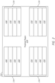
- FIG. 3 is a timing diagram of refresh operations in a memory device according to an embodiment of the present disclosure.
- the timing diagram 300 shows refresh operations over time (along the x-axis) for a variety of different memory banks.
- the memory banks may be the memory banks described as part of memory array 112 of FIG. 1 or memory banks 232 of FIG. 2 .
- the timing diagram 300 shows an example of how targeted refresh operations may be staggered between four different banks (BANK 0 -BANK 3 ). Other patterns of staggering targeted refresh operations between more or fewer banks may be used in other examples.
- the timing diagram 300 shows an example embodiment where five refresh operations are performed responsive to each activation of the refresh signal AREF.
- there may be five pumps e.g., activations of a pump signal in each refresh control circuit
- each of the pumps may be associated with either an auto-refresh operation or a targeted refresh operation.
- the pumps are represented in timing diagram 300 by the vertical lines.
- the pumps are in groups of 5 to represent the five pumps per AREF activation.
- the solid lines represent an auto-refresh operation, while the dashed lines represent a targeted refresh operation.
- more wordlines may be simultaneously refreshed in a bank during an auto-refresh operation than during a targeted refresh operation and thus an auto-refresh operation may draw more power than a targeted refresh operation.
- a given bank may perform a refresh operation responsive to each of the pumps. Since the banks produce the pumps responsive to a refresh signal (e.g., AREF) that they receive in common, the pumps may generally be synchronized. Thus, each of the banks may simultaneously perform a first pump, then simultaneously perform a second pump, etc. Each of the banks may generally perform auto-refresh operations responsive to the pumps and then may perform a number of targeted refresh operations responsive to a number of pumps, and then repeat the cycle.
- the targeted refresh operations may be staggered between the banks such that a first bank may begin performing targeted refresh operations at a first time, while a second bank may begin performing targeted refresh operations at a second time different from the first time.
- each of the banks may operate on the same cycle of auto and targeted refresh operations (e.g., n auto-refresh operations then m targeted refresh operations) and the only difference may be the phase of the cycle between the different banks.
- each bank there may be three auto-refresh operations and two targeted refresh operations.
- the first bank (BANK 0 ) performs 3 auto-refresh operations responsive to the first three pumps, and then two targeted refresh operations on pumps three and four.
- BANK 1 performs targeted refresh operations on pumps three and four.
- BANK 2 performs targeted refresh operations on pumps two and three.
- BANK 3 performs targeted refresh operations on pumps one and two.
- a second bank e.g., BANK 2
- a first bank e.g., BANK 3
- first pump respective auto-refresh pumps for BANK 0 - 2 , and one targeted refresh pump for BANK 3 ; fifth pump: respective auto-refresh pumps for BANK 1 - 3 , and one targeted refresh pump for BANK 0 ).
- second, third, and fourth pumps in each group two targeted refresh operations and two auto-refresh operations may be performed. Accordingly, at each simultaneous pump across the different banks, a portion of the banks may perform a targeted refresh operation while the remaining portion performs the auto-refresh operation. For example, there is no point where all four banks simultaneously perform either type of refresh operation.
- the banks BANK 0 -BANK 3 of FIG. 3 are shown as having a refresh cycle which is the same length as the number of pumps produced in response to each AREF. In some embodiments, the refresh cycle may be longer or shorter than the number of pumps produced responsive to each AREF. Similarly, the example embodiment of FIG. 3 shows that each group of pumps includes a mix of targeted and auto-refresh operations. In some embodiments, a bank may perform only one type of refresh operations responsive to a given AREF.
- the different types of refresh operation may be staggered between different activations of AREF rather than between different pumps.
- BANK 0 may perform a number of pumps, one or more of which is used to perform a targeted refresh operation
- BANKS 1 - 3 may perform a number of pumps each of which is used to perform auto-refresh operations.
- BANK 1 may perform one or more targeted refresh operations
- BANK 0 and BANK 2 - 3 perform auto-refresh operations.
- BANK 2 may perform one or more targeted refresh operations, while BANK 0 - 1 and BANK 3 may perform auto-refresh operations.
- BANK 3 may perform one or more targeted refresh operations, while BANKS 0 - 2 perform auto-refresh operations.
- FIG. 4 is a block diagram of a refresh control circuit according to an embodiment of the present disclosure.
- the refresh control circuit 416 may implement the refresh control circuit 116 of FIG. 1 in some embodiments.
- Certain internal components and signals of the refresh address control circuit 416 are shown to illustrate the operation of the refresh address control circuit 416 .
- the dotted line 432 is shown to represent that in certain embodiments, each of the components (e.g., the refresh address control circuit 416 and row decoder 408 ) may correspond to a particular bank of memory, and that these components may be repeated for each of the banks of memory.
- only components for a single bank will be described.
- An interface 431 may provide one or more signals to an address refresh control circuit 416 and row decoder 408 .
- the refresh address control circuit 416 may include a sample timing generator 438 , an address sampler 437 , a row hammer refresh (RHR) state controller 436 and a refresh address generator 439 .
- the interface 431 may provide one or more control signals, such as an auto-refresh signal AREF, and a row address XADD.
- the RHR state control 436 may determine if an auto-refresh or a targeted refresh operation should be performed.
- the RHR state control circuit 436 may indicate different refresh operations in different banks in order to stagger the targeted and auto-refresh operations between the banks.
- An RHR bank stagger circuit 435 may control the REIR state control circuit 436 to stagger the targeted and auto-refresh operations.
- the refresh address control circuit 416 shows components associated with a particular implementation of detecting aggressor addresses by sampling incoming values of the row address XADD at random or semi-random timing. Other methods of detecting aggressor addresses may be used in other embodiments, and other components may be provided in the refresh address control circuit 416 .
- the address sampler 437 may sample (e.g., latch) the current row address XADD responsive to an activation of ArmSample.
- the address sampler 437 may also provide one or more of the latched addresses to the refresh address generator 439 as the matched address HitXADD.
- the RHR state controller 436 may provide the signal RHR to indicate that a row hammer refresh operation (e.g., a refresh of the victim rows corresponding to an identified aggressor row) should occur.
- the RFER state controller 436 may also provide an internal refresh signal IREF, to indicate that an auto-refresh operation should occur.
- the RHR state controller 436 may be used to control the timings of targeted refresh operations and auto-refresh operations.
- the activations of IREF and RHR may represent activations of the pump signal.
- Each RHR state controller 436 may include internal logic which determines the timing with which it provides signals (e.g., RHR) to indicate if a targeted refresh or auto-refresh operation should be performed in the associated bank.
- each RHR state controller 436 may include a counter, and may provide the signal RHR based on a number of occurrences of the refresh signal AREF (and/or the number of occurrences of IREF).
- the counter in each RHR state controller 436 in each of the different banks may initialize to a different value to stagger the refresh operations. Accordingly, each RHR state controller 436 may produce the same pattern of targeted and auto-refresh operations, however those patterns may be out of phase with each other such that they are staggered in time.
- RHR bank stagger circuit 435 may provide a signal to the RHR state control circuits 436 to control the staggering.
- the RHR bank stagger circuit 435 may provide signals to each of the RHR state control circuit 436 associated with the different banks which may indicate when a targeted refresh operation should be performed.
- the RHR bank stagger circuit 435 may contain internal logic (e.g., counters initialized to different values) which allow it to direct the staggering between the different banks.
- the refresh address generator 439 may provide a refresh address RXADD, which may be an auto-refresh address or may be one or more victim addresses corresponding to victim rows of the aggressor row corresponding to the match address HitXADD.
- the row decoder 408 may perform a refresh operation responsive to the refresh address RXADD and the row hammer refresh signal RHR.
- the row decoder 408 may perform an auto-refresh operation based on the refresh address RXADD and the internal refresh signal IREF.
- the refresh address control circuit 416 may determine if one or more targeted refresh operations is currently needed, and may provide targeted refresh addresses when a targeted refresh operation is called for.
- the refresh address control circuits 416 associated with the different banks may each determine a number of targeted refresh operations to perform based on the characteristics of the accesses to the row addresses XADD (e.g., the number, frequency, and/or pattern of accesses). For example, a first refresh address control circuit 416 associated with a first bank containing multiple rows which are hammered may determine that there need to be more targeted refresh operations than a second refresh address control circuit 416 associated with a second bank containing less rows which are hammered.
- the refresh operations may occur in cycles (e.g., a certain number of pumps and/or a certain number of AREF occurrences), and the refresh address control circuit 416 may determine a number of targeted refresh operations to perform in each cycle. The remainder of the refresh operations in the cycle may be used for auto-refresh operations or other scheduled operations. Although different banks may determine different numbers of targeted refresh operations to perform, the targeted refresh operations may still be staggered between the different banks.
- the interface 431 may represent one or more components which provides signals to components of the bank.
- the interface 431 may represent components such as the command address input circuit 102 , the address decoder 104 , and/or the command control 106 of FIG. 1 .
- the interface 431 may provide a row address XADD, the auto-refresh signal AREF, an activation signal ACT, and a precharge signal Pre.
- the auto-refresh signal AREF may be a periodic signal which may indicate when an auto-refresh operation is to occur.
- the activation signal ACT may be provided to activate a given bank of the memory.
- the precharge signal Pre may be provided to precharge the given bank of the memory.
- the row address XADD may be a signal including multiple bits (which may be transmitted in series or in parallel) and may correspond to a specific row of an activated memory bank.
- the sample timing generator 438 provides the sampling signal ArmSample.
- ArmSample may alternate between a low logic level and a high logic level.
- An activation of Arm Sample may be a ‘pulse’, where ArmSample is raised to a high logic level and then returns to a low logic level.
- the interval between the pulses of ArmSample may be random, pseudo-random, and/or based on one or more signals of the device (e.g., AREF).
- the address sampler 437 may receive the row address XADD from the interface 431 and ArmSample from the sample timing generator 438 .
- the row address XADD may change as the interface 431 directs access operations (e.g., read and write operations) to different rows of the memory cell array memory cell array 112 of FIG. 1 ).
- the address sampler 437 may sample the current value of XADD.
- the address sampler 532 may provide the currently sampled value of XADD as the match address HitXADD.
- the refresh address generator 439 may provide one or more victim addresses associated with the match address HitXADD as the refresh address RXADD.
- the address sampler 437 may determine if one or more rows is an aggressor row based on the sampled row address XADD, and may provide identified aggressor rows as the match address HitXADD. As part of this determination, the address sampler 437 may record (e.g., by latching and/or storing in a register) the current value of XADD responsive to the activation of ArmSample. The current value of XADD may be compared to previously recorded addresses in the address sampler 437 (e.g., the addresses stored in the latch/register), to determine access patterns over time of the sampled addresses.
- the activation of ArmSample may also cause the address sampler 437 to provide the address of the aggressor row as a match address HitXADD.
- the match address (e.g., aggressor address) HitXADD may be stored in a latch circuit for later retrieval by the refresh address generator 439 .
- the value of one or more match addresses HitXADD may be stored until the signal RHR indicates a targeted refresh operation.
- the RHR state controller 436 may receive the auto-refresh signal AREF and provide the row hammer refresh signal RHR and the internal refresh signal IREF.
- the signal RHR may indicate that a targeted refresh operation should take place (e.g., that one or more victim rows associated with the identified aggressor HitXADD should be refreshed).
- the signal IREF may indicate that an auto-refresh operation should occur.
- the RHIR state controller 436 may use internal logic to provide the RHR signal.
- the RHR state controller 436 may include a counter and may provide the RHR signal based on certain number of activations of AREF (e.g., every 4 th activation of AREF).
- the counter may be initialized to a particular value when the memory is powered on). The particular value may vary from refresh control circuit to refresh control circuit between banks.
- the RHR state controller 436 may also provide an internal refresh signal IREF, which may control the timing of refresh operations.
- an internal refresh signal IREF may be used as a refresh pump signal to control the activations of refresh pumps.
- each activation of AREF may be associated with a number of activations of IREF, which may be associated with a number of refresh operations, which may be a mix of targeted refresh operations and auto-refresh operations.
- each activation of IREF may be associated with a refresh operation on the refresh address RXADD, while the state of RHR may determine if the refresh address RXADD is associated with an auto-refresh operation or a targeted refresh operation.
- the signal IREF may be used to indicate that an auto-refresh operation should occur, while the signal RHR is used to indicate that a targeted refresh operation should occur.
- the signals RHR and IREF may be generated such that they are not active at the same time (e.g., are not both at a high logic level at the same time) and each activation of IREF may be associated with an auto-refresh operation, while each activation of RHR may be associated with a targeted refresh operation.
- the RHR state controller 436 may count activations of IREF and use the count of IREF (e.g., the pumps) to determine when the signal RHR should be provided. Similar to previously described, the counter may initialize to a different value for different refresh control circuits. In some embodiments, the RHR state controller 436 may receive one or more signals from an RHR bank stagger circuit 435 , which may direct the different RHR state controllers 436 to provide the signal RHR. In either of these manner targeted and auto-refresh operations may be staggered between banks.
- the refresh address generator 439 may receive the row hammer refresh signal RHR and the match address HitXADD.
- the match address HitXADD may represent an aggressor row.
- the refresh address generator 439 may determine the locations of one or more victim rows based on the match address HitXADD and provide them as the refresh address RXADD.
- the victim rows may include rows which are physically adjacent to the aggressor row (e.g., HitXADD+1 and HitXADD ⁇ 1).
- the victim rows may also include rows which are physically adjacent to the physically adjacent rows of the aggressor row (e.g., HitXADD+2 and HitXADD ⁇ 2). Other relationships between victim rows and the identified aggressor rows may be used in other examples.
- the refresh address generator 439 may determine the value of the refresh address RXADD based on the row hammer refresh signal RHR. In some embodiments, when the signal RHR is not active, the refresh address generator 439 may provide one of a sequence of auto refresh addresses as the refresh address RXADD. When the signal RHR is active, the refresh address generator 439 may provide a targeted refresh address, such as a victim address, as the refresh address RXADD.
- the row decoder 408 may perform one or more operations on the memory array (not shown) based on the received signals and addresses. For example, responsive to the activation signal ACT and the row address XADD (and IREF and RHR being at a low logic level), the row decoder 408 may direct one or more access operations (for example, a read operation) on the specified row address XADD. Responsive to the RHR signal being active, the row decoder 408 may refresh the refresh address RXADD.
- FIG. 5 is a block diagram of a row decoder according to an embodiment of the present disclosure.
- the row decoder 500 may implement the row control 108 of FIG. 1 and/or the row decoder 408 of FIG. 4 in some embodiments of the disclosure.
- the row decoder 500 may determine whether to activate a word line of the memory bank (e.g., a bank of memory array 112 of FIG. 1 ) corresponding to the row address XADD or the refresh address RXADD.
- a word line of the memory bank e.g., a bank of memory array 112 of FIG. 1
- the row decoder 500 is provided with a row activation timing generator 542 , which receives the internal refresh signal IREF and the row hammer refresh signal RHR, the active signal ACT, and the pre-charge signal Pre and provides a state signal RefPD, a word-line actuation signal wdEn, a sense-amplifier actuation signal saEn, and a bit-line equalize signal BLEQ.
- the signals IREF and RHR may be the auto-refresh signal AREF.
- the state signal RefPD is supplied to a multiplexer 540 , which selects one of the row address XADD and the refresh address RXADD.
- An address XADDi selected by the multiplexer 540 is supplied to a row redundancy control circuit 544 . If the word line indicated by the address XADDi is replaced by a redundant word line, a hit signal RedMatch is activated, and a row address XADDd 1 , which is a replacement destination, is generated.
- the addresses XADDi and XADDd 1 are supplied to a multiplexer 546 ; wherein, if the hit signal RedMatch is not activated, the address XADDi is selected; and, if the hit signal RedMatch is activated, the address XADDd 1 is selected.
- the selected address XADD 2 is supplied to an X address decoder 548 .
- the address decoder 548 controls the operation of the word line indicated by the address XADD 2 , the sense amplifier corresponding thereto, an equalize circuit, etc. based on the word-line actuation signal wdEn, the sense-amplifier actuation signal saEn, and the bit-line equalize signal BLEQ.
Landscapes
- Engineering & Computer Science (AREA)
- Microelectronics & Electronic Packaging (AREA)
- Computer Hardware Design (AREA)
- Dram (AREA)
Abstract
Description
Claims (16)
Priority Applications (5)
| Application Number | Priority Date | Filing Date | Title |
|---|---|---|---|
| US16/375,716 US11227649B2 (en) | 2019-04-04 | 2019-04-04 | Apparatuses and methods for staggered timing of targeted refresh operations |
| CN202080030380.7A CN113728387B (en) | 2019-04-04 | 2020-04-03 | Apparatus and method for staggered timing of targeted refresh operations |
| KR1020217035609A KR102728395B1 (en) | 2019-04-04 | 2020-04-03 | Device and method for staggered timing of target refresh operations |
| PCT/US2020/026689 WO2020206333A1 (en) | 2019-04-04 | 2020-04-03 | Apparatuses and methods for staggered timing of targeted refresh operations |
| US17/187,002 US11309012B2 (en) | 2019-04-04 | 2021-02-26 | Apparatuses and methods for staggered timing of targeted refresh operations |
Applications Claiming Priority (1)
| Application Number | Priority Date | Filing Date | Title |
|---|---|---|---|
| US16/375,716 US11227649B2 (en) | 2019-04-04 | 2019-04-04 | Apparatuses and methods for staggered timing of targeted refresh operations |
Related Child Applications (1)
| Application Number | Title | Priority Date | Filing Date |
|---|---|---|---|
| US17/187,002 Continuation US11309012B2 (en) | 2019-04-04 | 2021-02-26 | Apparatuses and methods for staggered timing of targeted refresh operations |
Publications (2)
| Publication Number | Publication Date |
|---|---|
| US20200321049A1 US20200321049A1 (en) | 2020-10-08 |
| US11227649B2 true US11227649B2 (en) | 2022-01-18 |
Family
ID=72663231
Family Applications (2)
| Application Number | Title | Priority Date | Filing Date |
|---|---|---|---|
| US16/375,716 Active US11227649B2 (en) | 2019-04-04 | 2019-04-04 | Apparatuses and methods for staggered timing of targeted refresh operations |
| US17/187,002 Active US11309012B2 (en) | 2019-04-04 | 2021-02-26 | Apparatuses and methods for staggered timing of targeted refresh operations |
Family Applications After (1)
| Application Number | Title | Priority Date | Filing Date |
|---|---|---|---|
| US17/187,002 Active US11309012B2 (en) | 2019-04-04 | 2021-02-26 | Apparatuses and methods for staggered timing of targeted refresh operations |
Country Status (4)
| Country | Link |
|---|---|
| US (2) | US11227649B2 (en) |
| KR (1) | KR102728395B1 (en) |
| CN (1) | CN113728387B (en) |
| WO (1) | WO2020206333A1 (en) |
Cited By (15)
| Publication number | Priority date | Publication date | Assignee | Title |
|---|---|---|---|---|
| US11380382B2 (en) | 2020-08-19 | 2022-07-05 | Micron Technology, Inc. | Refresh logic circuit layout having aggressor detector circuit sampling circuit and row hammer refresh control circuit |
| US11417383B2 (en) | 2019-08-23 | 2022-08-16 | Micron Technology, Inc. | Apparatuses and methods for dynamic refresh allocation |
| US11532346B2 (en) | 2018-10-31 | 2022-12-20 | Micron Technology, Inc. | Apparatuses and methods for access based refresh timing |
| US11557331B2 (en) | 2020-09-23 | 2023-01-17 | Micron Technology, Inc. | Apparatuses and methods for controlling refresh operations |
| US11610622B2 (en) | 2019-06-05 | 2023-03-21 | Micron Technology, Inc. | Apparatuses and methods for staggered timing of skipped refresh operations |
| US11626152B2 (en) | 2018-05-24 | 2023-04-11 | Micron Technology, Inc. | Apparatuses and methods for pure-time, self adopt sampling for row hammer refresh sampling |
| US20230205872A1 (en) * | 2021-12-23 | 2023-06-29 | Advanced Micro Devices, Inc. | Method and apparatus to address row hammer attacks at a host processor |
| US11715512B2 (en) | 2019-10-16 | 2023-08-01 | Micron Technology, Inc. | Apparatuses and methods for dynamic targeted refresh steals |
| US11749331B2 (en) | 2020-08-19 | 2023-09-05 | Micron Technology, Inc. | Refresh modes for performing various refresh operation types |
| US11798610B2 (en) | 2019-06-04 | 2023-10-24 | Micron Technology, Inc. | Apparatuses and methods for controlling steal rates |
| US11810612B2 (en) | 2020-12-18 | 2023-11-07 | Micron Technology, Inc. | Apparatuses and methods for row hammer based cache lockdown |
| US11935576B2 (en) | 2018-12-03 | 2024-03-19 | Micron Technology, Inc. | Semiconductor device performing row hammer refresh operation |
| US12002501B2 (en) | 2018-12-26 | 2024-06-04 | Micron Technology, Inc. | Apparatuses and methods for distributed targeted refresh operations |
| US12112787B2 (en) | 2022-04-28 | 2024-10-08 | Micron Technology, Inc. | Apparatuses and methods for access based targeted refresh operations |
| US12125514B2 (en) | 2022-04-28 | 2024-10-22 | Micron Technology, Inc. | Apparatuses and methods for access based refresh operations |
Families Citing this family (34)
| Publication number | Priority date | Publication date | Assignee | Title |
|---|---|---|---|---|
| US10490251B2 (en) | 2017-01-30 | 2019-11-26 | Micron Technology, Inc. | Apparatuses and methods for distributing row hammer refresh events across a memory device |
| US10580475B2 (en) | 2018-01-22 | 2020-03-03 | Micron Technology, Inc. | Apparatuses and methods for calculating row hammer refresh addresses in a semiconductor device |
| US11152050B2 (en) | 2018-06-19 | 2021-10-19 | Micron Technology, Inc. | Apparatuses and methods for multiple row hammer refresh address sequences |
| US10573370B2 (en) | 2018-07-02 | 2020-02-25 | Micron Technology, Inc. | Apparatus and methods for triggering row hammer address sampling |
| CN111354393B (en) | 2018-12-21 | 2023-10-20 | 美光科技公司 | Apparatus and method for timing interleaving for targeted refresh operations |
| US10770127B2 (en) * | 2019-02-06 | 2020-09-08 | Micron Technology, Inc. | Apparatuses and methods for managing row access counts |
| US11615831B2 (en) | 2019-02-26 | 2023-03-28 | Micron Technology, Inc. | Apparatuses and methods for memory mat refresh sequencing |
| US11043254B2 (en) | 2019-03-19 | 2021-06-22 | Micron Technology, Inc. | Semiconductor device having cam that stores address signals |
| US11227649B2 (en) | 2019-04-04 | 2022-01-18 | Micron Technology, Inc. | Apparatuses and methods for staggered timing of targeted refresh operations |
| US11264096B2 (en) | 2019-05-14 | 2022-03-01 | Micron Technology, Inc. | Apparatuses, systems, and methods for a content addressable memory cell with latch and comparator circuits |
| US11158364B2 (en) | 2019-05-31 | 2021-10-26 | Micron Technology, Inc. | Apparatuses and methods for tracking victim rows |
| US11158373B2 (en) | 2019-06-11 | 2021-10-26 | Micron Technology, Inc. | Apparatuses, systems, and methods for determining extremum numerical values |
| US10832792B1 (en) | 2019-07-01 | 2020-11-10 | Micron Technology, Inc. | Apparatuses and methods for adjusting victim data |
| US11139015B2 (en) | 2019-07-01 | 2021-10-05 | Micron Technology, Inc. | Apparatuses and methods for monitoring word line accesses |
| US11386946B2 (en) | 2019-07-16 | 2022-07-12 | Micron Technology, Inc. | Apparatuses and methods for tracking row accesses |
| US10943636B1 (en) | 2019-08-20 | 2021-03-09 | Micron Technology, Inc. | Apparatuses and methods for analog row access tracking |
| US10964378B2 (en) | 2019-08-22 | 2021-03-30 | Micron Technology, Inc. | Apparatus and method including analog accumulator for determining row access rate and target row address used for refresh operation |
| KR102833439B1 (en) * | 2019-11-01 | 2025-07-10 | 삼성전자주식회사 | Memory device including processing element, and memory system including the memory device |
| US11276456B2 (en) | 2020-05-29 | 2022-03-15 | Micron Technology, Inc. | Systems and methods for capture and replacement of hammered word line address |
| US11309010B2 (en) | 2020-08-14 | 2022-04-19 | Micron Technology, Inc. | Apparatuses, systems, and methods for memory directed access pause |
| US11302376B2 (en) * | 2020-08-25 | 2022-04-12 | Micron Technology, Inc. | Systems and methods for memory refresh |
| US11222682B1 (en) | 2020-08-31 | 2022-01-11 | Micron Technology, Inc. | Apparatuses and methods for providing refresh addresses |
| US11222686B1 (en) | 2020-11-12 | 2022-01-11 | Micron Technology, Inc. | Apparatuses and methods for controlling refresh timing |
| US11462291B2 (en) | 2020-11-23 | 2022-10-04 | Micron Technology, Inc. | Apparatuses and methods for tracking word line accesses |
| US11482275B2 (en) | 2021-01-20 | 2022-10-25 | Micron Technology, Inc. | Apparatuses and methods for dynamically allocated aggressor detection |
| KR102827213B1 (en) | 2021-02-04 | 2025-07-01 | 삼성전자주식회사 | Memory Device skipping refresh operation and Operating Method thereof |
| KR102906228B1 (en) * | 2021-02-25 | 2025-12-30 | 삼성전자주식회사 | Memory Device and Operating Method thereof |
| US11600314B2 (en) | 2021-03-15 | 2023-03-07 | Micron Technology, Inc. | Apparatuses and methods for sketch circuits for refresh binning |
| EP4364139A4 (en) * | 2021-06-30 | 2025-04-30 | Rambus Inc. | DRAM REFRESH CONTROL WITH MASTER WORD LINE GRANULARITY OF REFRESH INTERVALS |
| US11664063B2 (en) | 2021-08-12 | 2023-05-30 | Micron Technology, Inc. | Apparatuses and methods for countering memory attacks |
| KR102892723B1 (en) | 2021-11-17 | 2025-11-28 | 삼성전자주식회사 | Memory device, memory system having the same and operating method thereof |
| US11688451B2 (en) | 2021-11-29 | 2023-06-27 | Micron Technology, Inc. | Apparatuses, systems, and methods for main sketch and slim sketch circuit for row address tracking |
| US12165687B2 (en) | 2021-12-29 | 2024-12-10 | Micron Technology, Inc. | Apparatuses and methods for row hammer counter mat |
| US11922031B1 (en) * | 2022-09-23 | 2024-03-05 | Micron Technology, Inc. | Apparatus with directed refresh management mechanism |
Citations (367)
| Publication number | Priority date | Publication date | Assignee | Title |
|---|---|---|---|---|
| US5299159A (en) | 1992-06-29 | 1994-03-29 | Texas Instruments Incorporated | Serial register stage arranged for connection with a single bitline |
| US5654929A (en) | 1995-09-14 | 1997-08-05 | Samsung Electronics Co., Ltd. | Refresh strategy for DRAMs |
| US5699297A (en) | 1995-05-30 | 1997-12-16 | Kabushiki Kaisha Toshiba | Method of rewriting data in a microprocessor additionally provided with a flash memory |
| US5867442A (en) * | 1995-12-21 | 1999-02-02 | Samsung Electronics Co., Ltd. | Variable output voltage booster circuits and methods |
| US5933377A (en) | 1997-03-25 | 1999-08-03 | Mitsubishi Denki Kabushiki Kaisha | Semiconductor memory device and defect repair method for semiconductor memory device |
| US5943283A (en) | 1997-12-05 | 1999-08-24 | Invox Technology | Address scrambling in a semiconductor memory |
| US5956288A (en) | 1997-12-22 | 1999-09-21 | Emc Corporation | Modular memory system with shared memory access |
| US5959923A (en) | 1990-06-19 | 1999-09-28 | Dell Usa, L.P. | Digital computer having a system for sequentially refreshing an expandable dynamic RAM memory circuit |
| US5970507A (en) | 1995-12-12 | 1999-10-19 | Mitsubishi Denki Kabushiki Kaisha | Semiconductor memory device having a refresh-cycle program circuit |
| US5999471A (en) * | 1997-01-30 | 1999-12-07 | Samsung Electronics, Co., Ltd. | Semiconductor memory device having a refresh function and a method for refreshing the same |
| US6002629A (en) | 1997-12-06 | 1999-12-14 | Samsung Electronics Co., Ltd. | Integrated circuit memory devices having improved refresh mode addressing and methods of operating same |
| US6011734A (en) | 1998-03-12 | 2000-01-04 | Motorola, Inc. | Fuseless memory repair system and method of operation |
| US6061290A (en) | 1997-06-30 | 2000-05-09 | Micron Technology, Inc. | Method and apparatus for simultaneous memory subarray testing |
| US6064621A (en) * | 1998-01-13 | 2000-05-16 | Mitsubishi Denki Kabushiki Kaisha | Multi-bank clock synchronous type semiconductor memory device having improved memory array and power supply arrangement |
| US6212118B1 (en) | 1997-12-12 | 2001-04-03 | Nec Corporation | Semiconductor memory |
| US20010008498A1 (en) | 1995-07-03 | 2001-07-19 | Mitsubishi Denki Kabushiki Kaisha | Fast accessible dynamic type semiconductor memory device |
| US6306721B1 (en) | 2001-03-16 | 2001-10-23 | Chartered Semiconductor Maufacturing Ltd. | Method of forming salicided poly to metal capacitor |
| US6310806B1 (en) | 1999-11-26 | 2001-10-30 | Kabushiki Kaisha Toshiba | Semiconductor memory device with redundant circuit |
| US20020026613A1 (en) | 2000-08-28 | 2002-02-28 | Mitsubishi Denki Kabushiki Kaisha | Semiconductor device capable of adjusting timing of input waveform by tester with high accuracy |
| US6363024B1 (en) | 1999-11-18 | 2002-03-26 | Infineon Technologies Ag | Method for carrying out auto refresh sequences on a DRAM |
| US6392952B1 (en) | 2001-05-15 | 2002-05-21 | United Microelectronics Corp. | Memory refresh circuit and memory refresh method |
| US6424582B1 (en) | 1998-05-27 | 2002-07-23 | Mitsubishi Denki Kasbushiki Kaisha | Semiconductor memory device having redundancy |
| US6434064B2 (en) | 2000-06-27 | 2002-08-13 | Kabushiki Kaisha Toshiba | Semiconductor memory device having redundancy circuit for saving faulty memory cells |
| US6452868B1 (en) | 1998-05-22 | 2002-09-17 | Micron Technology, Inc. | Method for generating memory addresses for accessing memory-cell arrays in memory devices |
| US20020181301A1 (en) | 1999-12-03 | 2002-12-05 | Hiroyuki Takahashi | Semiconductor storage and method for testing the same |
| US20020191467A1 (en) | 2001-06-15 | 2002-12-19 | Mitsubishi Denki Kabushiki Kaisha | Semiconductor memory device |
| US6515928B2 (en) | 2000-11-30 | 2003-02-04 | Fujitsu Limited | Semiconductor memory device having a plurality of low power consumption modes |
| US20030026161A1 (en) | 2001-08-03 | 2003-02-06 | Fujitsu Limited | Semiconductor memory |
| US6535950B1 (en) | 1999-06-10 | 2003-03-18 | Fujitsu Limited | Semiconductor memory device having a refresh operation |
| US20030063512A1 (en) | 2000-04-11 | 2003-04-03 | Hiroyuki Takahashi | Semiconductor storage device |
| US20030067825A1 (en) | 2001-10-05 | 2003-04-10 | Hiroki Shimano | Semiconductor memory device |
| US20030081483A1 (en) | 2001-09-19 | 2003-05-01 | Denise De Paor | Dram refresh command operation |
| US6567340B1 (en) | 1999-09-23 | 2003-05-20 | Netlogic Microsystems, Inc. | Memory storage cell based array of counters |
| US20030123301A1 (en) | 2001-12-28 | 2003-07-03 | Samsung Electronics Co., Ltd. | Semiconductor memory device post-repair circuit and method |
| US20030161208A1 (en) | 2002-02-25 | 2003-08-28 | Fujitsu Limited | Semiconductor memory device, refresh control method thereof, and test method thereof |
| US20030193829A1 (en) | 2002-04-11 | 2003-10-16 | Morgan Donald M. | Method and system for low power refresh of dynamic random access memories |
| US20030231540A1 (en) | 2002-06-18 | 2003-12-18 | Nanoamp Solutions, Inc. | DRAM with total self refresh and control circuit |
| US20040004856A1 (en) | 2002-07-04 | 2004-01-08 | Nec Corporation | Magnetic random access memory |
| US20040008544A1 (en) | 2002-07-15 | 2004-01-15 | Fujitsu Limited | Semiconductor memory |
| US20040022093A1 (en) | 2002-08-02 | 2004-02-05 | Lee Hi-Choon | Semiconductor memory device having improved replacement efficiency of defective word lines by redundancy word lines |
| US20040024955A1 (en) * | 2002-06-27 | 2004-02-05 | Patel Mukesh K. | Application processors and memory architecture for wireless applications |
| US20040114446A1 (en) | 2000-03-08 | 2004-06-17 | Hiroyuki Takahashi | Semiconductor memory |
| US20040130959A1 (en) | 2002-12-20 | 2004-07-08 | Nec Electronics Corporation | Semiconductor memory device having a DRAM cell structure and handled as a SRAM |
| US20040184323A1 (en) | 2003-03-17 | 2004-09-23 | Fujitsu Limited | Semiconductor memory device with shift register-based refresh address generation circuit |
| US20040218431A1 (en) | 2003-04-30 | 2004-11-04 | Hynix Semiconductor Inc. | Semiconductor memory device and method of operating the same |
| US20050002268A1 (en) * | 2003-05-16 | 2005-01-06 | Seiko Epson Corporation | Semiconductor memory device and electronic apparatus |
| US20050041502A1 (en) | 2003-08-18 | 2005-02-24 | Martin Perner | Circuit and method for evaluating and controlling a refresh rate of memory cells of a dynamic memory |
| US20050105362A1 (en) | 2003-11-14 | 2005-05-19 | Jong-Hyun Choi | Semiconductor memory device for performing refresh operation |
| US20050108460A1 (en) | 2003-11-14 | 2005-05-19 | Intel Corporation | Partial bank DRAM refresh |
| JP2005216429A (en) | 2004-01-30 | 2005-08-11 | Elpida Memory Inc | Semiconductor storage device and its refresh control method |
| US6950364B2 (en) | 2003-02-10 | 2005-09-27 | Hynix Semiconductor Inc. | Self-refresh apparatus and method |
| US20050213408A1 (en) | 2004-03-29 | 2005-09-29 | Taiwan Semiconductor Manufacturing Company, Ltd. | Ripple refresh circuit and method for sequentially refreshing a semiconductor memory system |
| US20050243627A1 (en) | 2004-04-29 | 2005-11-03 | Yun-Sang Lee | Semiconductor memory device with auto refresh to specified bank |
| US20050265104A1 (en) * | 2004-05-27 | 2005-12-01 | Remaklus Perry W Jr | Method and system for providing independent bank refresh for volatile memories |
| US20060018174A1 (en) | 2004-07-21 | 2006-01-26 | Taek-Seon Park | Semiconductor memory device performing auto refresh in the self refresh mode |
| US7002868B2 (en) | 2002-10-23 | 2006-02-21 | Nec Electronics Corporation | High-speed, two-port dynamic random access memory (DRAM) with a late-write configuration |
| US20060083099A1 (en) | 2004-10-14 | 2006-04-20 | Bae Myung H | System and method for redundancy memory decoding |
| US20060087903A1 (en) | 2004-10-21 | 2006-04-27 | Elpida Memory Inc. | Refresh control method of a semiconductor memory device and semiconductor memory device |
| US20060104139A1 (en) | 2004-11-15 | 2006-05-18 | Hwang Hur | Method of refreshing a memory device utilizing PASR and piled refresh schemes |
| US7057960B1 (en) | 2002-03-04 | 2006-06-06 | Cypress Semiconductor Corp. | Method and architecture for reducing the power consumption for memory devices in refresh operations |
| US7082070B2 (en) | 2003-07-23 | 2006-07-25 | Samsung Electronics Co., Ltd. | Temperature detection circuit and temperature detection method |
| US20060176744A1 (en) | 2005-02-10 | 2006-08-10 | Micron Technology, Inc. | Low power chip select (CS) latency option |
| US20060215474A1 (en) | 2005-03-25 | 2006-09-28 | Wolfgang Hokenmaier | Power saving refresh scheme for DRAMs with segmented word line architecture |
| US20060233012A1 (en) | 2005-03-30 | 2006-10-19 | Elpida Memory, Inc. | Semiconductor storage device having a plurality of stacked memory chips |
| US20060262616A1 (en) | 2005-05-18 | 2006-11-23 | Macronix International Co., Ltd. | Method and apparatus for implementing high speed memory |
| US20060262617A1 (en) * | 2005-05-18 | 2006-11-23 | Hynix Semiconductor Inc. | Page access circuit of semiconductor memory device |
| US20060268643A1 (en) * | 2005-05-31 | 2006-11-30 | John Schreck | System and method for hidden-refresh rate modification |
| US20070002651A1 (en) * | 2005-06-30 | 2007-01-04 | Hynix Semiconductor Inc. | Synchronous pseudo static random access memory |
| US20070008799A1 (en) | 2005-06-01 | 2007-01-11 | Elpida Memory, Inc | Semiconductor device |
| US20070014175A1 (en) | 2005-07-13 | 2007-01-18 | Samsung Electronics Co., Ltd. | DRAM and method for partially refreshing memory cell array |
| US20070028068A1 (en) | 2005-07-29 | 2007-02-01 | International Business Machines Corporation | System and method for managing resources in a distributed storage system |
| US20070030746A1 (en) | 2005-08-04 | 2007-02-08 | Best Scott C | Memory device testing to support address-differentiated refresh rates |
| US7187607B2 (en) | 2003-10-09 | 2007-03-06 | Elpida Memory, Inc. | Semiconductor memory device and method for manufacturing same |
| US7203115B2 (en) | 2003-08-18 | 2007-04-10 | Fujitsu Limited | Semiconductor memory and method for operating the same |
| US7203113B2 (en) | 2004-03-30 | 2007-04-10 | Nec Electronics Corporation | Semiconductor storage device |
| US7215588B2 (en) | 2004-04-28 | 2007-05-08 | Hynix Semiconductor Inc. | Apparatus for controlling self-refresh period in memory device |
| US20070147154A1 (en) | 2005-12-28 | 2007-06-28 | Hynix Semiconductor Inc. | Semiconductor Device |
| CN101038785A (en) | 2000-07-07 | 2007-09-19 | 睦塞德技术公司 | A high speed dram architecture with uniform access latency |
| US20070237016A1 (en) | 2004-06-23 | 2007-10-11 | Sanyo Electric Co., Ltd. | Memory |
| CN101067972A (en) | 2007-04-23 | 2007-11-07 | 北京芯技佳易微电子科技有限公司 | Memory error-detecting and error-correcting coding circuit and method for reading and writing data utilizing the same |
| US20070263442A1 (en) | 2006-05-15 | 2007-11-15 | Apple Inc. | Off-Die Charge Pump that Supplies Multiple Flash Devices |
| US20070297252A1 (en) | 2006-06-26 | 2007-12-27 | Anant Pratap Singh | Integrated circuit having memory array including ECC and/or column redundancy, and method of programming, controlling and/or operating same |
| US20080028260A1 (en) | 2006-07-26 | 2008-01-31 | Mutsumi Oyagi | Memory system |
| US20080031068A1 (en) | 2006-07-26 | 2008-02-07 | Zmos Technology, Inc. | Dynamic memory refresh configurations and leakage control methods |
| US20080126893A1 (en) | 2006-07-03 | 2008-05-29 | Stmicroelectronics Sa | Method of refreshing a dynamic random access memory and corresponding dynamic random access memory device, in particular incorporated into a cellular mobile telephone |
| US20080130394A1 (en) | 2006-12-05 | 2008-06-05 | Elpida Memory, Inc. | Semiconductor memory device |
| US20080181048A1 (en) | 2007-01-25 | 2008-07-31 | Yong-Joo Han | Semiconductor memory device and memory cell accessing method thereof |
| US20080212386A1 (en) | 2006-12-26 | 2008-09-04 | Elpida Memory, Inc. | Semiconductor memory device, semiconductor device, memory system and refresh control method |
| US20080224742A1 (en) | 2007-03-16 | 2008-09-18 | Pomichter Gerald P | Small scale clock multiplier circuit for fixed speed testing |
| US20080253212A1 (en) | 2007-04-10 | 2008-10-16 | Masahisa Iida | Semiconductor memory device |
| US20080253213A1 (en) | 2003-02-27 | 2008-10-16 | Fujitsu Limited | Semiconductor memory device and refresh method for the same |
| US20080270683A1 (en) | 2007-04-25 | 2008-10-30 | International Business Machines Corporation | Systems and methods for a dram concurrent refresh engine with processor interface |
| US20080266990A1 (en) | 2007-04-30 | 2008-10-30 | Infineon Technologies North America Corp. | Flexible redundancy replacement scheme for semiconductor device |
| US20080306723A1 (en) * | 2007-06-08 | 2008-12-11 | Luca De Ambroggi | Emulated Combination Memory Device |
| US20080316645A1 (en) | 2007-06-25 | 2008-12-25 | Samsung Electronics Co., Ltd. | Perpendicular magnetic recording head and method of manufacturing the same |
| US20090021999A1 (en) | 2007-07-20 | 2009-01-22 | Elpida Memory, Inc. | Semiconductor device |
| US20090052264A1 (en) | 2007-08-20 | 2009-02-26 | Hynix Semiconductor Inc. | Refresh characteristic testing circuit and method for testing refresh using the same |
| US20090059641A1 (en) | 2007-08-29 | 2009-03-05 | Jeddeloh Joe M | Memory device interface methods, apparatus, and systems |
| US20090073760A1 (en) | 2007-09-17 | 2009-03-19 | Yoram Betser | Minimizing read disturb in an array flash cell |
| US7551502B2 (en) | 2005-05-18 | 2009-06-23 | Elpida Memory, Inc. | Semiconductor device |
| US20090161468A1 (en) * | 2007-12-19 | 2009-06-25 | Fujitsu Microelectronics Limited | Semiconductor memory, memory system, and memory access control method |
| US20090168571A1 (en) | 2005-11-29 | 2009-07-02 | Samsung Electronics Co., Ltd. | Dynamic random access memory device and method of determining refresh cycle thereof |
| US20090185440A1 (en) | 2006-02-10 | 2009-07-23 | Hynix Semiconductor Inc. | Active cycyle control circuit for semiconductor memory apparatus |
| US20090201752A1 (en) | 2008-02-08 | 2009-08-13 | Elpida Memory, Inc. | Semiconductor memory device |
| US20090228739A1 (en) | 2007-11-25 | 2009-09-10 | Itzic Cohen | Recovery while programming non-volatile memory (nvm) |
| US20090251971A1 (en) | 2008-04-04 | 2009-10-08 | Kabushiki Kaisha Toshiba | Non-volatile semiconductor storage device and memory system |
| US20090296510A1 (en) | 2008-05-30 | 2009-12-03 | Samsung Electronics Co., Ltd. | Semiconductor memory device having refresh circuit and word line activating method therefor |
| US20100005376A1 (en) | 2008-07-02 | 2010-01-07 | Micron Technology, Inc. | Method and apparatus for repairing high capacity/high bandwidth memory devices |
| US20100061153A1 (en) | 2008-09-09 | 2010-03-11 | Ching-Fang Yen | Refresh Method for a Non-volatile Memory |
| US20100074042A1 (en) | 2008-09-24 | 2010-03-25 | Kabushiki Kaisha Toshiba | Semiconductor memory device |
| US20100097870A1 (en) | 2008-10-16 | 2010-04-22 | Jun-Bae Kim | Semiconductor memory device for controlling operation of delay-locked loop circuit |
| US20100110809A1 (en) | 2007-07-11 | 2010-05-06 | Fujitsu Microelectronics Limited | Semiconductor memory device and system with redundant element |
| US20100110810A1 (en) | 2007-07-11 | 2010-05-06 | Fujitsu Microelectronics Limited | Semiconductor memory device and system |
| US20100124138A1 (en) | 2008-11-17 | 2010-05-20 | Dong-Hyuk Lee | Semiconductor memory device having variable-mode refresh operation |
| US20100131812A1 (en) | 2008-11-26 | 2010-05-27 | Qualcomm Incorporated | Resizable Cache Memory |
| US20100128547A1 (en) | 2005-07-26 | 2010-05-27 | Elpida Memory, Inc. | Semiconductor memory device and refresh control method of memory system |
| US20100141309A1 (en) | 2008-12-05 | 2010-06-10 | Hynix Semiconductor Inc. | Initialization circuit and bank active circuit using the same |
| US20100157693A1 (en) | 2008-12-24 | 2010-06-24 | Kabushiki Kaisha Toshiba | Semiconductor memory device |
| US20100182862A1 (en) | 2009-01-21 | 2010-07-22 | Elpida Memory, Inc. | Semiconductor memory device and method of controlling auto-refresh |
| US20100182863A1 (en) | 2009-01-20 | 2010-07-22 | Elpida Memory, Inc. | Semiconductor memory device |
| US20100329069A1 (en) | 2009-06-26 | 2010-12-30 | Fujitsu Limited | Semiconductor memory device |
| US20110026290A1 (en) | 2009-08-03 | 2011-02-03 | Elpida Memory, Inc. | Semiconductor device having memory cell array divided into plural memory mats |
| US20110055495A1 (en) | 2009-08-28 | 2011-03-03 | Qualcomm Incorporated | Memory Controller Page Management Devices, Systems, and Methods |
| US20110069572A1 (en) | 2009-09-18 | 2011-03-24 | Samsung Electronics Co., Ltd. | Row address code selection based on locations of substandard memory cells |
| US20110122987A1 (en) | 2004-12-23 | 2011-05-26 | Braun Gmbh | Replaceable Accessory for a Small Electrical Appliance and Method of Monitoring the Usage of the Accessory |
| US20110134715A1 (en) | 2007-08-16 | 2011-06-09 | Unity Semiconductor Corporation | Method for accessing vertically stacked embedded non-flash re-writable non-volatile memory |
| US20110216614A1 (en) | 2010-03-05 | 2011-09-08 | Elpida Memory, Inc. | Semiconductor device enabling refreshing of redundant memory cell instead of defective memory cell |
| US20110225355A1 (en) * | 2010-03-12 | 2011-09-15 | Elpida Memory Inc. | Semiconductor device, refresh control method thereof and computer system |
| US20110299352A1 (en) | 2010-06-07 | 2011-12-08 | Elpida Memory, Inc. | Semiconductor device including memory cells that require refresh operation |
| US20110310648A1 (en) | 2010-06-21 | 2011-12-22 | Renesas Technology Corporation | Semiconductor storage device |
| US20120014199A1 (en) | 2010-07-15 | 2012-01-19 | Elpida Memory, Inc. | Semiconductor device that performs refresh operation |
| US20120059984A1 (en) | 2010-09-03 | 2012-03-08 | Kang Uk-Song | Semiconductor memory device |
| JP4911510B2 (en) | 2007-04-16 | 2012-04-04 | エルピーダメモリ株式会社 | Semiconductor memory device |
| US8174921B2 (en) | 2008-12-19 | 2012-05-08 | Samsung Electronics Co., Ltd. | Semiconductor memory device having shared temperature control circuit |
| US20120151131A1 (en) | 2010-12-09 | 2012-06-14 | International Business Machines Corporation | Memory system with a programmable refresh cycle |
| US20120155173A1 (en) * | 2010-12-13 | 2012-06-21 | Peter Wung Lee | Universal Timing Waveforms Sets to Improve Random Access Read and Write Speed of Memories |
| US20120155206A1 (en) | 2010-12-16 | 2012-06-21 | Elpida Memory, Inc. | Semiconductor device periodically updating delay locked loop circuit |
| US20120213021A1 (en) | 2011-02-18 | 2012-08-23 | Elpida Memory, Inc. | Semiconductor device having redundant bit line provided to replace defective bit line |
| US20120254472A1 (en) | 2010-03-15 | 2012-10-04 | Ware Frederick A | Chip selection in a symmetric interconnection topology |
| US20120287727A1 (en) | 2011-05-09 | 2012-11-15 | Inphi Corporation | Dram refresh method and system |
| US20120307582A1 (en) | 2011-06-02 | 2012-12-06 | Elpida Memory, Inc. | Semiconductor device performing self refresh operation |
| US20120327734A1 (en) | 2011-06-27 | 2012-12-27 | Fujitsu Semiconductor Limited | Semiconductor memory, system, and method of operating semiconductor memory |
| US20130003477A1 (en) | 2011-06-30 | 2013-01-03 | Ju-Seop Park | Semiconductor memory device including spare antifuse array and antifuse repair method of the semiconductor memory device |
| US20130003467A1 (en) | 2004-07-15 | 2013-01-03 | Micron Technology, Inc. | Digit line comparison circuits |
| JP2013004158A (en) | 2011-06-21 | 2013-01-07 | Elpida Memory Inc | Semiconductor storage device and refresh control method thereof |
| US20130028034A1 (en) | 2011-07-28 | 2013-01-31 | Elpida Memory, Inc. | Information processing system including semiconductor device having self-refresh mode |
| US20130051157A1 (en) | 2011-08-30 | 2013-02-28 | Hynix Semiconductor Inc. | Semiconductor memory device and refresh method thereof |
| US20130051171A1 (en) * | 2011-08-24 | 2013-02-28 | Micron Technology, Inc. | Memory refresh methods, memory section control circuits, and apparatuses |
| US8400805B2 (en) | 2011-01-28 | 2013-03-19 | Elpida Memory, Inc. | Semiconductor device |
| US20130077423A1 (en) | 2011-09-23 | 2013-03-28 | Hynix Semiconductor Inc. | Refresh method and apparatus for a semiconductor memory device |
| US20130279284A1 (en) | 2012-04-18 | 2013-10-24 | Samsung Electronics Co., Ltd. | Semiconductor memory device and method for refreshing memory cells |
| US8572423B1 (en) | 2010-06-22 | 2013-10-29 | Apple Inc. | Reducing peak current in memory systems |
| US20140006700A1 (en) | 2012-06-28 | 2014-01-02 | Andre Schaefer | Configuration for power reduction in dram |
| US20140006703A1 (en) | 2012-06-30 | 2014-01-02 | Kuljit S. Bains | Row hammer refresh command |
| US20140006704A1 (en) | 2012-06-30 | 2014-01-02 | Zvika Greenfield | Row hammer condition monitoring |
| US20140013185A1 (en) | 2012-03-30 | 2014-01-09 | Darshan Kobla | On chip redundancy repair for memory devices |
| US20140013169A1 (en) | 2012-03-30 | 2014-01-09 | Darshan Kobla | Generic address scrambler for memory circuit test engine |
| US20140016422A1 (en) | 2012-07-12 | 2014-01-16 | Jung-Sik Kim | Semiconductor memory device that controls refresh period, memory system and operating method thereof |
| US20140022858A1 (en) * | 2012-07-20 | 2014-01-23 | Ho-Yin Chen | Method of controlling a refresh operation of psram and related device |
| US20140043888A1 (en) * | 2012-08-10 | 2014-02-13 | Etron Technology, Inc. | Method of operating psram and related memory device |
| US20140050004A1 (en) | 2012-08-14 | 2014-02-20 | Elpida Memory, Inc. | Semiconductor device having hierarchically structured bit lines |
| US20140078841A1 (en) | 2012-09-18 | 2014-03-20 | Mosys, Inc. | Programmable memory built in self repair circuit |
| US20140078842A1 (en) | 2012-09-18 | 2014-03-20 | Samsung Electronics Co., Ltd. | Post package repairing method, method of preventing multiple activation of spare word lines, and semiconductor memory device including fuse programming circuit |
| US20140089576A1 (en) | 2012-09-24 | 2014-03-27 | Kuljit S. Bains | Method, apparatus and system for providing a memory refresh |
| US20140089758A1 (en) | 2012-09-27 | 2014-03-27 | Zion S. Kwok | Method, apparatus and system for handling data faults |
| US20140095780A1 (en) | 2012-09-28 | 2014-04-03 | Kuljit S. Bains | Distributed row hammer tracking |
| US20140095786A1 (en) | 2012-09-28 | 2014-04-03 | SK Hynix Inc. | Semiconductor device and operating method thereof |
| US20140119091A1 (en) | 2012-10-25 | 2014-05-01 | Samsung Electronics Co., Ltd. | Bit-line sense amplifier, semiconductor memory device and memory system including the same |
| US20140143473A1 (en) * | 2012-11-19 | 2014-05-22 | Spansion Llc | Data refresh in non-volatile memory |
| US20140169114A1 (en) | 2012-12-13 | 2014-06-19 | Samsung Electronics Co., Ltd. | Volatile memory devices, memory systems including the same and related methods |
| US20140181453A1 (en) | 2012-12-20 | 2014-06-26 | Advanced Micro Devices, Inc. | Processor with Host and Slave Operating Modes Stacked with Memory |
| US20140177370A1 (en) | 2012-12-21 | 2014-06-26 | Intel Corporation | Method, apparatus and system for responding to a row hammer event |
| US20140185403A1 (en) | 2012-12-28 | 2014-07-03 | Mediatek Inc. | Refresh method for switching between different refresh types based on at least one parameter of volatile memory and related memory controller |
| US20140189228A1 (en) | 2012-12-28 | 2014-07-03 | Zaika Greenfield | Throttling support for row-hammer counters |
| WO2014120477A1 (en) | 2013-02-04 | 2014-08-07 | Micron Technology, Inc. | Apparatuses and methods for targeted refreshing of memory |
| US20140219042A1 (en) | 2013-02-07 | 2014-08-07 | Samsung Electronics Co., Ltd. | Memory device and method of refreshing in a memory device |
| US8811100B2 (en) | 2012-06-28 | 2014-08-19 | SK Hynix Inc. | Cell array and memory device including the same |
| US20140237307A1 (en) | 2011-12-28 | 2014-08-21 | Darshan Kobla | Generic address scrambler for memory circuit test engine |
| US20140241099A1 (en) | 2013-02-26 | 2014-08-28 | Samsung Electronics Co., Ltd. | Semiconductor memory and memory system including the semiconductor memory |
| US20140254298A1 (en) | 2013-03-11 | 2014-09-11 | Nvidia Corporation | Variable dynamic memory refresh |
| US20140281206A1 (en) | 2013-03-15 | 2014-09-18 | John H. Crawford | Techniques for Probabilistic Dynamic Random Access Memory Row Repair |
| US20140281207A1 (en) | 2013-03-12 | 2014-09-18 | Sreenivas Mandava | Techniques for Determining Victim Row Addresses in a Volatile Memory |
| US8862973B2 (en) | 2009-12-09 | 2014-10-14 | Intel Corporation | Method and system for error management in a memory device |
| US20140321226A1 (en) | 2007-09-14 | 2014-10-30 | Conversant Intellectual Property Management Inc. | Dynamic random access memory and boosted voltage producer therefor |
| US20150016203A1 (en) | 2013-07-12 | 2015-01-15 | Qualcomm Incorporated | Dram sub-array level autonomic refresh memory controller optimization |
| US20150049566A1 (en) | 2013-08-13 | 2015-02-19 | SK Hynix Inc. | Memory and memory system including the same |
| US20150049567A1 (en) | 2013-08-14 | 2015-02-19 | SK Hynix Inc. | Memory and memory system including the same |
| US20150055420A1 (en) | 2013-08-26 | 2015-02-26 | Micron Technology, Inc. | Apparatuses and methods for selective row refreshes |
| US20150078112A1 (en) | 2013-09-19 | 2015-03-19 | Elite Semiconductor Memory Technology Inc. | Method for auto-refreshing memory cells in semiconductor memory device and semiconductor memory device using the method |
| US20150089326A1 (en) | 2013-09-25 | 2015-03-26 | SK Hynix Inc. | Address detection circuit and memory including the same |
| US20150092508A1 (en) * | 2013-09-27 | 2015-04-02 | Kuljit S. Bains | Directed per bank refresh command |
| US20150109871A1 (en) | 2012-11-30 | 2015-04-23 | Kuljit Bains | Row hammer monitoring based on stored row hammer threshold value |
| US9032141B2 (en) | 2012-11-30 | 2015-05-12 | Intel Corporation | Row hammer monitoring based on stored row hammer threshold value |
| US20150134897A1 (en) | 2013-11-11 | 2015-05-14 | Qualcomm Incorporated | Method and apparatus for refreshing a memory cell |
| US20150162064A1 (en) | 2013-12-09 | 2015-06-11 | SK Hynix Inc. | Refresh control circuit of semiconductor apparatus and refresh method using the same |
| US20150170728A1 (en) | 2013-12-18 | 2015-06-18 | SK Hynix Inc. | Memory and memory system including the same |
| US9076499B2 (en) | 2012-12-28 | 2015-07-07 | Intel Corporation | Refresh rate performance based on in-system weak bit detection |
| US9087602B2 (en) | 2013-05-30 | 2015-07-21 | Samsung Electronics Co., Ltd. | Volatile memory device capable of relieving disturbances of adjacent memory cells and refresh method thereof |
| US20150213872A1 (en) | 2014-01-30 | 2015-07-30 | Micron Technology, Inc. | Apparatuses and methods for address detection |
| US9117544B2 (en) | 2012-06-30 | 2015-08-25 | Intel Corporation | Row hammer refresh command |
| US9123447B2 (en) | 2013-08-09 | 2015-09-01 | SK Hynix Inc. | Memory, memory system including the same and method for operating memory |
| US20150255140A1 (en) | 2014-03-07 | 2015-09-10 | SK Hynix Inc. | Semiconductor memory device and refresh control system |
| US20150279442A1 (en) | 2014-03-26 | 2015-10-01 | SK Hynix Inc. | Semiconductor memory device and semiconductor memory system including the same |
| US9153294B2 (en) | 2012-09-24 | 2015-10-06 | Samsung Electronics Co., Ltd. | Semiconductor memory device having adjustable refresh period, memory system comprising same, and method of operating same |
| US20150294711A1 (en) | 2012-10-22 | 2015-10-15 | Hewlett-Packard Development Company, L.P. | Performing refresh of a memory device in response to access of data |
| US20150340077A1 (en) | 2014-05-21 | 2015-11-26 | Micron Technology, Inc. | Apparatuses and methods for controlling refresh operations |
| US20150356048A1 (en) | 2014-06-09 | 2015-12-10 | Micron Technology, Inc. | Method and apparatus for controlling access to a common bus by multiple components |
| US20150380073A1 (en) | 2014-06-25 | 2015-12-31 | SK Hynix Inc. | Memory device |
| US20160019940A1 (en) | 2014-07-21 | 2016-01-21 | SK Hynix Inc. | Memory device |
| US20160027498A1 (en) | 2014-07-24 | 2016-01-28 | Rambus Inc. | Reduced refresh power |
| US20160027532A1 (en) | 2014-07-22 | 2016-01-28 | SK Hynix Inc. | Memory device |
| US20160033479A1 (en) | 2010-07-22 | 2016-02-04 | Ramot At Tel Aviv University Ltd. | Systems and methods for detection of cellular stress |
| US20160042782A1 (en) | 2013-03-15 | 2016-02-11 | Ps4 Luxco S.A.R.L. | Semiconductor storage device and system provided with same |
| US20160070483A1 (en) | 2013-05-30 | 2016-03-10 | Hewlett-Packard Development, L.P. | Separate memory controllers to access data in memory |
| US20160078911A1 (en) | 2013-11-08 | 2016-03-17 | Micron Technology, Inc. | Semiconductor memory device having count value control circuit |
| US20160078846A1 (en) | 2014-09-17 | 2016-03-17 | Mediatek Inc. | Processor for use in dynamic refresh rate switching and related electronic device and method |
| US20160086649A1 (en) | 2014-09-23 | 2016-03-24 | SK Hynix Inc. | Smart refresh device |
| US20160093402A1 (en) | 2014-09-30 | 2016-03-31 | Sony Corporation | Memory with distributed replacement word lines |
| US9311985B2 (en) | 2013-12-18 | 2016-04-12 | SK Hynix Inc. | Memory and memory system for periodic targeted refresh |
| US20160125931A1 (en) | 2014-11-03 | 2016-05-05 | Samsung Electronics Co., Ltd. | Semiconductor memory device that performs a refresh operation |
| US20160133314A1 (en) | 2014-11-11 | 2016-05-12 | Samsung Electronics Co., Ltd. | Semiconductor memory devices, memory systems including the same, and methods of operating memory systems |
| US20160155491A1 (en) | 2014-11-27 | 2016-06-02 | Advanced Micro Devices, Inc. | Memory persistence management control |
| US20160180921A1 (en) | 2012-05-17 | 2016-06-23 | Samsung Electronics Co., Ltd. | Semiconductor memory device controlling refresh cycle, memory system, and method of operating the semiconductor memory device |
| US20160180917A1 (en) | 2014-12-23 | 2016-06-23 | Zeshan A. Chishti | Techniques to Reduce Memory Cell Refreshes for a Memory Device |
| US20160196863A1 (en) | 2015-01-07 | 2016-07-07 | Samsung Electronics Co., Ltd. | Method of operating memory device and method of operating memory system including the same |
| US20160202926A1 (en) | 2013-09-27 | 2016-07-14 | Hewlett Packard Enterprise Development Lp | Refresh row address |
| US9396786B2 (en) | 2013-09-25 | 2016-07-19 | SK Hynix Inc. | Memory and memory system including the same |
| US9406358B1 (en) | 2015-01-30 | 2016-08-02 | SK Hynix Inc. | Driving circuit and driving method using the same |
| US9424907B2 (en) | 2013-06-26 | 2016-08-23 | Micron Technology, Inc. | Semiconductor device suppressing BTI deterioration |
| US9484079B2 (en) | 2015-02-02 | 2016-11-01 | SK Hynix Inc. | Memory device and memory system including the same |
| US20160343423A1 (en) | 2015-05-18 | 2016-11-24 | Micron Technology, Inc. | Apparatus having dice to perorm refresh operations |
| US20170011792A1 (en) | 2015-07-06 | 2017-01-12 | Samsung Electronics Co., Ltd. | Embedded refresh controllers and memory devices including the same |
| US9570143B2 (en) | 2015-05-08 | 2017-02-14 | SK Hynix Inc. | Semiconductor memory device for performing refresh operation |
| US9570201B2 (en) * | 2015-04-17 | 2017-02-14 | Micron Technology, Inc. | Repair of memory devices using volatile and non-volatile memory |
| US20170052722A1 (en) | 2009-01-22 | 2017-02-23 | Rambus Inc. | Maintenance Operations in a DRAM |
| US20170111792A1 (en) | 2015-10-19 | 2017-04-20 | Vodafone Gmbh | Triggering a usage of a service of a mobile packet core network |
| US9646672B1 (en) | 2016-04-25 | 2017-05-09 | SK Hynix Inc. | Memory device and method of refreshing the same |
| US20170133085A1 (en) * | 2015-11-06 | 2017-05-11 | Samsung Electronics Co., Ltd. | Memory device and memory system performing request-based refresh, and operating method of the memory device |
| US9653139B1 (en) | 2016-04-01 | 2017-05-16 | SK Hynix Inc. | Simultaneous plural wordline within a bank refreshing control device and memory device including the same |
| US20170140811A1 (en) | 2015-11-18 | 2017-05-18 | SK Hynix Inc. | Refresh control circuit and memory device including same |
| US20170140810A1 (en) | 2015-11-17 | 2017-05-18 | Samsung Electronics Co., Ltd. | Memory device and memory system including the same for controlling collision between access operation and refresh operation |
| US20170140807A1 (en) * | 2014-07-03 | 2017-05-18 | Yale University | Circuitry for Ferroelectric FET-Based Dynamic Random Access Memory and Non-Violatile Memory |
| US20170148504A1 (en) * | 2015-11-24 | 2017-05-25 | Qualcomm Incorporated | Controlling a refresh mode of a dynamic random access memory (dram) die |
| US20170146598A1 (en) | 2015-11-23 | 2017-05-25 | SK Hynix Inc. | Stacked memory device and semiconductor memory system including the same |
| US9672889B2 (en) | 2014-12-08 | 2017-06-06 | SK Hynix Inc. | Semiconductor memory device and refresh control method thereof |
| US9685240B1 (en) | 2016-03-17 | 2017-06-20 | SK Hynix Inc. | Memory device to alleviate the effects of row hammer condition and memory system including the same |
| US9691466B1 (en) | 2016-06-03 | 2017-06-27 | SK Hynix Inc. | Memory device including refresh controller |
| US20170186481A1 (en) * | 2015-12-28 | 2017-06-29 | Samsung Electronics Co., Ltd. | Refresh controller and memory device including the same |
| US9697913B1 (en) | 2016-06-10 | 2017-07-04 | Micron Technology, Inc. | Ferroelectric memory cell recovery |
| US20170213586A1 (en) | 2016-01-25 | 2017-07-27 | Samsung Electronics Co., Ltd. | Memory device performing hammer refresh operation and memory system including the same |
| US9734887B1 (en) | 2016-03-21 | 2017-08-15 | International Business Machines Corporation | Per-die based memory refresh control based on a master controller |
| US9741447B2 (en) | 2014-04-23 | 2017-08-22 | Micron Technology, Inc. | Semiconductor device including fuse circuit |
| US9761297B1 (en) | 2016-12-30 | 2017-09-12 | Intel Corporation | Hidden refresh control in dynamic random access memory |
| US20170263305A1 (en) | 2014-11-25 | 2017-09-14 | Samg Yeun CHO | Method of detecting most frequently accessed address of semiconductor memory based on probability information |
| US20170269861A1 (en) | 2016-03-17 | 2017-09-21 | Mediatek Inc. | Dynamic rank switching for low power volatile memory |
| WO2017171927A1 (en) | 2016-03-31 | 2017-10-05 | Micron Technology, Inc. | Semiconductor device |
| US9786351B2 (en) | 2015-12-29 | 2017-10-10 | SK Hynix Inc. | Semiconductor memory device for performing refresh operation and operating method therof |
| US9799391B1 (en) | 2016-11-21 | 2017-10-24 | Nanya Technology Corporation | Dram circuit, redundant refresh circuit and refresh method |
| US9805782B1 (en) | 2017-02-02 | 2017-10-31 | Elite Semiconductor Memory Technology Inc. | Memory device capable of determining candidate wordline for refresh and control method thereof |
| US9812185B2 (en) | 2015-10-21 | 2017-11-07 | Invensas Corporation | DRAM adjacent row disturb mitigation |
| US9818469B1 (en) | 2016-09-05 | 2017-11-14 | SK Hynix Inc. | Refresh control device and semiconductor device including the same |
| US9831003B2 (en) * | 2012-02-29 | 2017-11-28 | Samsung Electronics Co., Ltd. | Device and method for repairing memory cell and memory system including the device |
| US20170345482A1 (en) | 2016-05-25 | 2017-11-30 | Advanced Micro Devices, Inc. | Fine granularity refresh |
| US20170352404A1 (en) | 2016-06-01 | 2017-12-07 | SK Hynix Inc. | Refresh control device, and memory device including the same |
| US20180005690A1 (en) | 2016-06-29 | 2018-01-04 | Micron Technology, Inc. | Oscillator controlled random sampling method and circuit |
| US9865328B1 (en) | 2015-12-04 | 2018-01-09 | Integrated Device Technology, Inc. | Nullifying incorrect sampled data contribution in decision feedback equalizer at restart of forwarded clock in memory system |
| US20180025773A1 (en) * | 2015-02-28 | 2018-01-25 | Intel Corporation | Precharging and refreshing banks in memory device with bank group architecture |
| US20180025772A1 (en) * | 2016-07-25 | 2018-01-25 | SK Hynix Inc. | Semiconductor devices having a refresh operation |
| JP6281030B1 (en) | 2017-08-02 | 2018-02-14 | ゼンテルジャパン株式会社 | Semiconductor memory device |
| US20180047110A1 (en) | 2013-11-07 | 2018-02-15 | Aaron BLACKMAN | System, method, and program product for calculating premiums for employer-based supplemental unemployment insurance |
| US20180061476A1 (en) | 2016-08-23 | 2018-03-01 | SK Hynix Inc. | Refresh control circuit for target refresh operation of semiconductor memory device, and operating method thereof |
| US20180075927A1 (en) | 2016-09-09 | 2018-03-15 | Samsung Electronics Co., Ltd. | Memory apparatus including a command controller |
| US9934143B2 (en) | 2013-09-26 | 2018-04-03 | Intel Corporation | Mapping a physical address differently to different memory devices in a group |
| CN107871516A (en) | 2016-09-26 | 2018-04-03 | 爱思开海力士有限公司 | Refresh Control Device |
| US20180096719A1 (en) | 2016-09-30 | 2018-04-05 | Intel Corporation | Staggering initiation of refresh in a group of memory devices |
| US20180108401A1 (en) | 2016-10-17 | 2018-04-19 | SK Hynix Inc. | Memory device |
| US20180114565A1 (en) | 2016-10-20 | 2018-04-26 | SK Hynix Inc. | Refresh timing generation circuit, refresh control circuit and semiconductor apparatus including the same |
| US20180122454A1 (en) | 2016-10-31 | 2018-05-03 | SK Hynix Inc. | Address counting circuit, memory device and operating method thereof |
| US20180130506A1 (en) | 2016-11-06 | 2018-05-10 | Intel Corporation | Memory device with flexible internal data write control circuitry |
| US20180137005A1 (en) | 2016-11-15 | 2018-05-17 | Intel Corporation | Increased redundancy in multi-device memory package to improve reliability |
| US9978430B2 (en) | 2012-04-24 | 2018-05-22 | Samsung Electronics Co., Ltd. | Memory devices providing a refresh request and memory controllers responsive to a refresh request |
| US20180158507A1 (en) | 2016-12-06 | 2018-06-07 | Jong-Min BANG | Memory device and memory system performing a hammer refresh operation and associated operations |
| US20180182445A1 (en) | 2016-12-26 | 2018-06-28 | SK Hynix Inc. | Memory device, memory system including the same, and operation method thereof |
| US10020045B2 (en) | 2013-11-26 | 2018-07-10 | Micron Technology, Inc. | Partial access mode for dynamic random access memory |
| US10020046B1 (en) | 2017-03-03 | 2018-07-10 | Micron Technology, Inc. | Stack refresh control for memory device |
| US20180218767A1 (en) | 2017-01-30 | 2018-08-02 | Micron Technology, Inc. | Apparatuses and methods for distributing row hammer refresh events across a memory device |
| US20180226119A1 (en) | 2017-02-09 | 2018-08-09 | SK Hynix Inc. | Semiconductor device |
| US10049716B2 (en) | 1999-02-13 | 2018-08-14 | Intellectual Ventures I Llc | Refresh request queuing circuitry |
| US20180233197A1 (en) | 2017-02-16 | 2018-08-16 | Micron Technology, Inc. | Efficient utilization of memory die area |
| US20180240511A1 (en) * | 2013-07-31 | 2018-08-23 | Micron Technology, Inc. | Semiconductor device |
| US20180247876A1 (en) | 2017-02-28 | 2018-08-30 | SK Hynix Inc. | Stacked semiconductor device |
| US20180254078A1 (en) * | 2017-03-02 | 2018-09-06 | SK Hynix Inc. | Semiconductor device and method of driving the same |
| US20180261268A1 (en) | 2017-03-07 | 2018-09-13 | SK Hynix Inc. | Semiconductor device and semiconductor system |
| US20180276150A1 (en) | 2017-03-24 | 2018-09-27 | Advanced Micro Devices, Inc. | Dynamic memory remapping to reduce row-buffer conflicts |
| US10090038B2 (en) | 2015-05-13 | 2018-10-02 | Samsung Electronics Co., Ltd. | Semiconductor memory device for deconcentrating refresh commands and system including the same |
| US20180285007A1 (en) | 2017-04-04 | 2018-10-04 | Sandisk Technologies Llc | Memory maintenance operations during refresh window |
| US20180294028A1 (en) * | 2017-04-11 | 2018-10-11 | SK Hynix Inc. | Semiconductor memory device |
| US10141042B1 (en) | 2017-05-23 | 2018-11-27 | Micron Technology, Inc. | Method and apparatus for precharge and refresh control |
| US10170174B1 (en) | 2017-10-27 | 2019-01-01 | Micron Technology, Inc. | Apparatus and methods for refreshing memory |
| US10192608B2 (en) | 2017-05-23 | 2019-01-29 | Micron Technology, Inc. | Apparatuses and methods for detection refresh starvation of a memory |
| US20190043558A1 (en) * | 2017-08-02 | 2019-02-07 | Qualcomm Incorporated | Partial refresh technique to save memory refresh power |
| US20190065087A1 (en) | 2017-08-23 | 2019-02-28 | Qualcomm Incorporated | Systems and methods for memory power saving via kernel steering to memory balloons |
| US20190066766A1 (en) * | 2017-08-31 | 2019-02-28 | Micron Technology, Inc. | Systems and methods for refreshing a memory bank while accessing another memory bank using a shared address path |
| US20190066759A1 (en) | 2018-11-01 | 2019-02-28 | Intel Corporation | Row hammer mitigation with randomization of target row selection |
| US20190088316A1 (en) | 2017-09-19 | 2019-03-21 | Toshiba Memory Corporation | Resistance change type memory |
| US20190088315A1 (en) | 2017-09-20 | 2019-03-21 | Sandisk Technologies Llc | Identifying non-volatile memory cells for data refresh |
| US20190115069A1 (en) | 2017-10-12 | 2019-04-18 | Winbond Electronics Corp. | Volatile memory storage apparatus and refresh method thereof |
| US20190122723A1 (en) | 2017-10-20 | 2019-04-25 | Micron Technology, Inc. | Apparatus and methods for refreshing memory |
| US20190129651A1 (en) | 2017-10-26 | 2019-05-02 | Advanced Micro Devices, Inc. | Swizzling in 3d stacked memory |
| US20190130960A1 (en) | 2017-10-26 | 2019-05-02 | SK Hynix Inc. | Memory systems and methods of controlling refresh operations of memory systems |
| US20190147964A1 (en) | 2017-11-13 | 2019-05-16 | Samsung Electronics Co., Ltd. | Memory device including massbit counter and method of operating the same |
| US10297305B1 (en) | 2017-10-30 | 2019-05-21 | SK Hynix Inc. | Memory device having twin cell mode and refresh method thereof |
| US10297307B1 (en) | 2017-12-29 | 2019-05-21 | Micron Technology, Inc. | Methods for independent memory bank maintenance and memory devices and systems employing the same |
| US20190161341A1 (en) | 2017-11-28 | 2019-05-30 | Micron Technology, Inc. | Systems and methods for temperature sensor access in die stacks |
| US20190190341A1 (en) | 2016-06-28 | 2019-06-20 | Huntsman Advanced Materials Licensing (Switzerland) Gmbh | Electrical Insulation System Based on Epoxy Resins for Generators and Motors |
| US20190198099A1 (en) | 2017-12-22 | 2019-06-27 | Micron Technology, Inc. | Auto-referenced memory cell read techniques |
| US20190198078A1 (en) | 2017-12-27 | 2019-06-27 | Spin Transfer Technologies, Inc. | Shared bit line array architecture for magnetoresistive memory |
| US20190196730A1 (en) | 2017-12-21 | 2019-06-27 | Qualcomm Incorporated | Partial area self refresh mode |
| US20190205253A1 (en) | 2017-12-29 | 2019-07-04 | Advanced Micro Devices, Inc. | Method and apparatus for controlling cache line storage in cache memory |
| US20190228815A1 (en) | 2018-01-22 | 2019-07-25 | Micron Technology, Inc. | Apparatuses and methods for calculating row hammer refresh addresses in a semiconductor device |
| US10381327B2 (en) | 2016-10-06 | 2019-08-13 | Sandisk Technologies Llc | Non-volatile memory system with wide I/O memory die |
| US20190252020A1 (en) | 2016-09-30 | 2019-08-15 | Intel Corporation | Two transistor, one resistor non-volatile gain cell memory and storage element |
| US20190279706A1 (en) * | 2018-03-07 | 2019-09-12 | SK Hynix Inc. | Refresh control circuit, semiconductor memory device, and refresh method thereof |
| US10446256B2 (en) * | 2008-04-09 | 2019-10-15 | Rambus Inc. | Controller to detect malfunctioning address of memory device |
| US20190333573A1 (en) | 2018-04-25 | 2019-10-31 | Samsung Electronics Co., Ltd. | Semiconductor memory device and memory system having the same |
| US10468076B1 (en) | 2018-08-17 | 2019-11-05 | Micron Technology, Inc. | Redundancy area refresh rate increase |
| US20190348103A1 (en) | 2018-05-11 | 2019-11-14 | SK Hynix Inc. | Semiconductor system including a counting circuit block |
| US20190348102A1 (en) | 2018-05-08 | 2019-11-14 | Micron Technology, Inc. | Memory with internal refresh rate control |
| US10490250B1 (en) | 2018-08-14 | 2019-11-26 | Micron Technology, Inc. | Apparatuses for refreshing memory of a semiconductor device |
| US10504577B1 (en) | 2018-11-05 | 2019-12-10 | Micron Technology, Inc. | Apparatus with a row hit rate/refresh management mechanism |
| US10510396B1 (en) | 2018-06-19 | 2019-12-17 | Apple Inc. | Method and apparatus for interrupting memory bank refresh |
| US20190385667A1 (en) | 2018-06-19 | 2019-12-19 | Micron Technology, Inc. | Apparatuses and methods for multiple row hammer refresh address sequences |
| US20190385668A1 (en) * | 2018-06-14 | 2019-12-19 | Winbond Electronics Corp. | Dynamic random access memory |
| US20190385670A1 (en) | 2018-06-19 | 2019-12-19 | Apple Inc. | Method and Apparatus for Optimizing Calibrations of a Memory Subsystem |
| US20190386557A1 (en) | 2018-06-15 | 2019-12-19 | Ford Global Technologies, Llc | Virtual resistance gate driver |
| US20190385661A1 (en) * | 2018-06-19 | 2019-12-19 | SK Hynix Inc. | Semiconductor device |
| US20190391760A1 (en) * | 2018-06-25 | 2019-12-26 | Toshiba Memory Corporation | Memory system |
| US20190392886A1 (en) | 2016-10-31 | 2019-12-26 | Intel Corporation | Applying chip select for memory device identification and power management control |
| US20200051616A1 (en) | 2018-08-09 | 2020-02-13 | SK Hynix Inc. | Memory device, memory system, and method for refreshing memory device |
| US10572377B1 (en) | 2018-09-19 | 2020-02-25 | Micron Technology, Inc. | Row hammer refresh for content addressable memory devices |
| US10573370B2 (en) | 2018-07-02 | 2020-02-25 | Micron Technology, Inc. | Apparatus and methods for triggering row hammer address sampling |
| US20200075086A1 (en) * | 2018-09-04 | 2020-03-05 | Winbond Electronics Corp. | Memory device and refresh method for psram |
| US10607679B2 (en) * | 2018-04-19 | 2020-03-31 | Winbond Electronics Corp. | Memory device and refreshing method thereof |
| US20200126611A1 (en) | 2018-10-17 | 2020-04-23 | Micron Technology, Inc. | Semiconductor device performing refresh operation in deep sleep mode |
| US20200135263A1 (en) | 2018-10-31 | 2020-04-30 | Micron Technology, Inc. | Apparatuses and methods for access based refresh timing |
| US20200143871A1 (en) | 2017-12-18 | 2020-05-07 | SK Hynix Inc. | Data storage device and operating method thereof |
| WO2020117686A1 (en) | 2018-12-03 | 2020-06-11 | Micron Technology, Inc. | Semiconductor device performing row hammer refresh operation |
| US20200185026A1 (en) | 2018-12-06 | 2020-06-11 | SK Hynix Inc. | Semiconductor memory device and operating method thereof |
| US20200194056A1 (en) * | 2018-12-12 | 2020-06-18 | Micron Technology, Inc. | Apparatuses and methods for multi-bank and multi-pump refresh operations |
| US10699796B2 (en) * | 2014-05-27 | 2020-06-30 | Hewlett Packard Enterprise Development Lp | Validation of a repair to a selected row of data |
| US20200210278A1 (en) * | 2018-12-31 | 2020-07-02 | Micron Technology, Inc. | Error correction in row hammer mitigation and target row refresh |
| US20200211633A1 (en) | 2018-12-27 | 2020-07-02 | Micron Technology, Inc. | Apparatus with a row-hammer address latch mechanism |
| US20200211632A1 (en) | 2018-12-26 | 2020-07-02 | Micron Technology, Inc. | Apparatuses and methods for distributed targeted refresh operations |
| US20200219555A1 (en) * | 2018-12-21 | 2020-07-09 | Micron Technology, Inc. | Apparatuses and methods for staggered timing of targeted refresh operations |
| US20200273517A1 (en) | 2019-02-26 | 2020-08-27 | Micron Technology, Inc. | Apparatuses and methods for memory mat refresh sequencing |
| US20200279599A1 (en) * | 2002-06-20 | 2020-09-03 | Rambus Inc. | Dynamic Memory Supporting Simultaneous Refresh and Data-Access Transactions |
| US20200294569A1 (en) | 2018-05-24 | 2020-09-17 | Micron Technology, Inc. | Apparatuses and methods for pure-time, self adopt sampling for row hammer refresh sampling |
| US10790005B1 (en) | 2019-04-26 | 2020-09-29 | Micron Technology, Inc. | Techniques for reducing row hammer refresh |
| US10832792B1 (en) | 2019-07-01 | 2020-11-10 | Micron Technology, Inc. | Apparatuses and methods for adjusting victim data |
| US20200381040A1 (en) | 2019-05-31 | 2020-12-03 | Micron Technology, Inc. | Apparatuses and methods for tracking victim rows |
| WO2020247163A1 (en) | 2019-06-04 | 2020-12-10 | Micron Technology, Inc. | Apparatuses and methods for controlling steal rates |
| US20200388324A1 (en) | 2019-06-05 | 2020-12-10 | Micron Technology, Inc. | Apparatuses and methods for staggered timing of skipped refresh operations |
| US20210057021A1 (en) | 2019-08-20 | 2021-02-25 | Micron Technology, Inc. | Apparatuses and methods for analog row access tracking |
| US20210057022A1 (en) | 2019-08-23 | 2021-02-25 | Micron Technology, Inc. | Apparatuses and methods for dynamic refresh allocation |
| US10964378B2 (en) * | 2019-08-22 | 2021-03-30 | Micron Technology, Inc. | Apparatus and method including analog accumulator for determining row access rate and target row address used for refresh operation |
| US20210118491A1 (en) | 2019-10-16 | 2021-04-22 | Micron Technology, Inc. | Apparatuses and methods for dynamic targeted refresh steals |
| US20210183435A1 (en) | 2019-04-04 | 2021-06-17 | Micron Technology, Inc. | Apparatuses and methods for staggered timing of targeted refresh operations |
Family Cites Families (22)
| Publication number | Priority date | Publication date | Assignee | Title |
|---|---|---|---|---|
| WO1999046775A2 (en) | 1998-03-10 | 1999-09-16 | Rambus, Inc. | Performing concurrent refresh and current control operations in a memory subsystem |
| JP2005216423A (en) | 2004-01-30 | 2005-08-11 | Denji Oyo Kenkyusho | Compound type cylinder storage |
| US7565479B2 (en) | 2005-08-04 | 2009-07-21 | Rambus Inc. | Memory with refresh cycle donation to accommodate low-retention-storage rows |
| TWI335035B (en) | 2007-06-20 | 2010-12-21 | Etron Technology Inc | Memory row scheme having memory row redundancy repair function |
| US8289760B2 (en) | 2008-07-02 | 2012-10-16 | Micron Technology, Inc. | Multi-mode memory device and method having stacked memory dice, a logic die and a command processing circuit and operating in direct and indirect modes |
| US9286965B2 (en) | 2010-12-03 | 2016-03-15 | Rambus Inc. | Memory refresh method and devices |
| US8645777B2 (en) | 2011-12-29 | 2014-02-04 | Intel Corporation | Boundary scan chain for stacked memory |
| CN102663155B (en) * | 2012-03-09 | 2014-05-28 | 中国科学院微电子研究所 | Method and device for optimizing layout gate length |
| CN102931187A (en) * | 2012-10-25 | 2013-02-13 | 北京七芯中创科技有限公司 | Layout structure of temperature compensation clock chip |
| KR102157769B1 (en) * | 2013-10-28 | 2020-09-18 | 에스케이하이닉스 주식회사 | Memory system and method for operating the same |
| KR102124973B1 (en) | 2013-12-11 | 2020-06-22 | 에스케이하이닉스 주식회사 | Memory and memory system including the same |
| US9535831B2 (en) | 2014-01-10 | 2017-01-03 | Advanced Micro Devices, Inc. | Page migration in a 3D stacked hybrid memory |
| KR102168115B1 (en) * | 2014-01-21 | 2020-10-20 | 에스케이하이닉스 주식회사 | Memory and memory system including the same |
| KR20170055222A (en) * | 2015-11-11 | 2017-05-19 | 삼성전자주식회사 | Memory device and memory system having repair unit modification function |
| US10048877B2 (en) | 2015-12-21 | 2018-08-14 | Intel Corporation | Predictive memory maintenance |
| US9928895B2 (en) | 2016-02-03 | 2018-03-27 | Samsung Electronics Co., Ltd. | Volatile memory device and electronic device comprising refresh information generator, information providing method thereof, and refresh control method thereof |
| US10725677B2 (en) | 2016-02-19 | 2020-07-28 | Sandisk Technologies Llc | Systems and methods for efficient power state transitions |
| US10468087B2 (en) | 2016-07-28 | 2019-11-05 | Micron Technology, Inc. | Apparatuses and methods for operations in a self-refresh state |
| US10354714B2 (en) | 2016-08-23 | 2019-07-16 | Micron Technology, Inc. | Temperature-dependent refresh circuit configured to increase or decrease a count value of a refresh timer according to a self-refresh signal |
| KR102632534B1 (en) | 2016-09-20 | 2024-02-05 | 에스케이하이닉스 주식회사 | Address decoder, active control circuit and semiconductor memory including the same |
| US20180102776A1 (en) | 2016-10-07 | 2018-04-12 | Altera Corporation | Methods and apparatus for managing application-specific power gating on multichip packages |
| US10452480B2 (en) | 2017-05-25 | 2019-10-22 | Micron Technology, Inc. | Memory device with dynamic processing level calibration |
-
2019
- 2019-04-04 US US16/375,716 patent/US11227649B2/en active Active
-
2020
- 2020-04-03 WO PCT/US2020/026689 patent/WO2020206333A1/en not_active Ceased
- 2020-04-03 CN CN202080030380.7A patent/CN113728387B/en active Active
- 2020-04-03 KR KR1020217035609A patent/KR102728395B1/en active Active
-
2021
- 2021-02-26 US US17/187,002 patent/US11309012B2/en active Active
Patent Citations (451)
| Publication number | Priority date | Publication date | Assignee | Title |
|---|---|---|---|---|
| US5959923A (en) | 1990-06-19 | 1999-09-28 | Dell Usa, L.P. | Digital computer having a system for sequentially refreshing an expandable dynamic RAM memory circuit |
| US5299159A (en) | 1992-06-29 | 1994-03-29 | Texas Instruments Incorporated | Serial register stage arranged for connection with a single bitline |
| US5699297A (en) | 1995-05-30 | 1997-12-16 | Kabushiki Kaisha Toshiba | Method of rewriting data in a microprocessor additionally provided with a flash memory |
| US20010008498A1 (en) | 1995-07-03 | 2001-07-19 | Mitsubishi Denki Kabushiki Kaisha | Fast accessible dynamic type semiconductor memory device |
| US5654929A (en) | 1995-09-14 | 1997-08-05 | Samsung Electronics Co., Ltd. | Refresh strategy for DRAMs |
| US5970507A (en) | 1995-12-12 | 1999-10-19 | Mitsubishi Denki Kabushiki Kaisha | Semiconductor memory device having a refresh-cycle program circuit |
| US5867442A (en) * | 1995-12-21 | 1999-02-02 | Samsung Electronics Co., Ltd. | Variable output voltage booster circuits and methods |
| US5999471A (en) * | 1997-01-30 | 1999-12-07 | Samsung Electronics, Co., Ltd. | Semiconductor memory device having a refresh function and a method for refreshing the same |
| US5933377A (en) | 1997-03-25 | 1999-08-03 | Mitsubishi Denki Kabushiki Kaisha | Semiconductor memory device and defect repair method for semiconductor memory device |
| US6061290A (en) | 1997-06-30 | 2000-05-09 | Micron Technology, Inc. | Method and apparatus for simultaneous memory subarray testing |
| US5943283A (en) | 1997-12-05 | 1999-08-24 | Invox Technology | Address scrambling in a semiconductor memory |
| US6002629A (en) | 1997-12-06 | 1999-12-14 | Samsung Electronics Co., Ltd. | Integrated circuit memory devices having improved refresh mode addressing and methods of operating same |
| US6212118B1 (en) | 1997-12-12 | 2001-04-03 | Nec Corporation | Semiconductor memory |
| US5956288A (en) | 1997-12-22 | 1999-09-21 | Emc Corporation | Modular memory system with shared memory access |
| US6064621A (en) * | 1998-01-13 | 2000-05-16 | Mitsubishi Denki Kabushiki Kaisha | Multi-bank clock synchronous type semiconductor memory device having improved memory array and power supply arrangement |
| US6011734A (en) | 1998-03-12 | 2000-01-04 | Motorola, Inc. | Fuseless memory repair system and method of operation |
| US6452868B1 (en) | 1998-05-22 | 2002-09-17 | Micron Technology, Inc. | Method for generating memory addresses for accessing memory-cell arrays in memory devices |
| US6424582B1 (en) | 1998-05-27 | 2002-07-23 | Mitsubishi Denki Kasbushiki Kaisha | Semiconductor memory device having redundancy |
| US10049716B2 (en) | 1999-02-13 | 2018-08-14 | Intellectual Ventures I Llc | Refresh request queuing circuitry |
| US6535950B1 (en) | 1999-06-10 | 2003-03-18 | Fujitsu Limited | Semiconductor memory device having a refresh operation |
| US6567340B1 (en) | 1999-09-23 | 2003-05-20 | Netlogic Microsystems, Inc. | Memory storage cell based array of counters |
| US6363024B1 (en) | 1999-11-18 | 2002-03-26 | Infineon Technologies Ag | Method for carrying out auto refresh sequences on a DRAM |
| US6310806B1 (en) | 1999-11-26 | 2001-10-30 | Kabushiki Kaisha Toshiba | Semiconductor memory device with redundant circuit |
| US20020181301A1 (en) | 1999-12-03 | 2002-12-05 | Hiroyuki Takahashi | Semiconductor storage and method for testing the same |
| US20040114446A1 (en) | 2000-03-08 | 2004-06-17 | Hiroyuki Takahashi | Semiconductor memory |
| US20030063512A1 (en) | 2000-04-11 | 2003-04-03 | Hiroyuki Takahashi | Semiconductor storage device |
| US6434064B2 (en) | 2000-06-27 | 2002-08-13 | Kabushiki Kaisha Toshiba | Semiconductor memory device having redundancy circuit for saving faulty memory cells |
| CN101038785A (en) | 2000-07-07 | 2007-09-19 | 睦塞德技术公司 | A high speed dram architecture with uniform access latency |
| US20020026613A1 (en) | 2000-08-28 | 2002-02-28 | Mitsubishi Denki Kabushiki Kaisha | Semiconductor device capable of adjusting timing of input waveform by tester with high accuracy |
| US6515928B2 (en) | 2000-11-30 | 2003-02-04 | Fujitsu Limited | Semiconductor memory device having a plurality of low power consumption modes |
| US6306721B1 (en) | 2001-03-16 | 2001-10-23 | Chartered Semiconductor Maufacturing Ltd. | Method of forming salicided poly to metal capacitor |
| US6392952B1 (en) | 2001-05-15 | 2002-05-21 | United Microelectronics Corp. | Memory refresh circuit and memory refresh method |
| US20020191467A1 (en) | 2001-06-15 | 2002-12-19 | Mitsubishi Denki Kabushiki Kaisha | Semiconductor memory device |
| US20030026161A1 (en) | 2001-08-03 | 2003-02-06 | Fujitsu Limited | Semiconductor memory |
| US20030081483A1 (en) | 2001-09-19 | 2003-05-01 | Denise De Paor | Dram refresh command operation |
| US20030067825A1 (en) | 2001-10-05 | 2003-04-10 | Hiroki Shimano | Semiconductor memory device |
| US20030123301A1 (en) | 2001-12-28 | 2003-07-03 | Samsung Electronics Co., Ltd. | Semiconductor memory device post-repair circuit and method |
| US20030161208A1 (en) | 2002-02-25 | 2003-08-28 | Fujitsu Limited | Semiconductor memory device, refresh control method thereof, and test method thereof |
| US7057960B1 (en) | 2002-03-04 | 2006-06-06 | Cypress Semiconductor Corp. | Method and architecture for reducing the power consumption for memory devices in refresh operations |
| US20030193829A1 (en) | 2002-04-11 | 2003-10-16 | Morgan Donald M. | Method and system for low power refresh of dynamic random access memories |
| US20030231540A1 (en) | 2002-06-18 | 2003-12-18 | Nanoamp Solutions, Inc. | DRAM with total self refresh and control circuit |
| US20200279599A1 (en) * | 2002-06-20 | 2020-09-03 | Rambus Inc. | Dynamic Memory Supporting Simultaneous Refresh and Data-Access Transactions |
| US20040024955A1 (en) * | 2002-06-27 | 2004-02-05 | Patel Mukesh K. | Application processors and memory architecture for wireless applications |
| US20040004856A1 (en) | 2002-07-04 | 2004-01-08 | Nec Corporation | Magnetic random access memory |
| US20040008544A1 (en) | 2002-07-15 | 2004-01-15 | Fujitsu Limited | Semiconductor memory |
| US7209402B2 (en) | 2002-07-15 | 2007-04-24 | Fujitsu Limited | Semiconductor memory |
| US20040022093A1 (en) | 2002-08-02 | 2004-02-05 | Lee Hi-Choon | Semiconductor memory device having improved replacement efficiency of defective word lines by redundancy word lines |
| US7002868B2 (en) | 2002-10-23 | 2006-02-21 | Nec Electronics Corporation | High-speed, two-port dynamic random access memory (DRAM) with a late-write configuration |
| US20040130959A1 (en) | 2002-12-20 | 2004-07-08 | Nec Electronics Corporation | Semiconductor memory device having a DRAM cell structure and handled as a SRAM |
| US6950364B2 (en) | 2003-02-10 | 2005-09-27 | Hynix Semiconductor Inc. | Self-refresh apparatus and method |
| US20080253213A1 (en) | 2003-02-27 | 2008-10-16 | Fujitsu Limited | Semiconductor memory device and refresh method for the same |
| US20040184323A1 (en) | 2003-03-17 | 2004-09-23 | Fujitsu Limited | Semiconductor memory device with shift register-based refresh address generation circuit |
| US20040218431A1 (en) | 2003-04-30 | 2004-11-04 | Hynix Semiconductor Inc. | Semiconductor memory device and method of operating the same |
| US20050002268A1 (en) * | 2003-05-16 | 2005-01-06 | Seiko Epson Corporation | Semiconductor memory device and electronic apparatus |
| US7082070B2 (en) | 2003-07-23 | 2006-07-25 | Samsung Electronics Co., Ltd. | Temperature detection circuit and temperature detection method |
| US7203115B2 (en) | 2003-08-18 | 2007-04-10 | Fujitsu Limited | Semiconductor memory and method for operating the same |
| US20050041502A1 (en) | 2003-08-18 | 2005-02-24 | Martin Perner | Circuit and method for evaluating and controlling a refresh rate of memory cells of a dynamic memory |
| US7187607B2 (en) | 2003-10-09 | 2007-03-06 | Elpida Memory, Inc. | Semiconductor memory device and method for manufacturing same |
| US20050108460A1 (en) | 2003-11-14 | 2005-05-19 | Intel Corporation | Partial bank DRAM refresh |
| US20050105362A1 (en) | 2003-11-14 | 2005-05-19 | Jong-Hyun Choi | Semiconductor memory device for performing refresh operation |
| JP2005216429A (en) | 2004-01-30 | 2005-08-11 | Elpida Memory Inc | Semiconductor storage device and its refresh control method |
| US20050213408A1 (en) | 2004-03-29 | 2005-09-29 | Taiwan Semiconductor Manufacturing Company, Ltd. | Ripple refresh circuit and method for sequentially refreshing a semiconductor memory system |
| US7203113B2 (en) | 2004-03-30 | 2007-04-10 | Nec Electronics Corporation | Semiconductor storage device |
| US7215588B2 (en) | 2004-04-28 | 2007-05-08 | Hynix Semiconductor Inc. | Apparatus for controlling self-refresh period in memory device |
| US20050243627A1 (en) | 2004-04-29 | 2005-11-03 | Yun-Sang Lee | Semiconductor memory device with auto refresh to specified bank |
| US20050265104A1 (en) * | 2004-05-27 | 2005-12-01 | Remaklus Perry W Jr | Method and system for providing independent bank refresh for volatile memories |
| US20070237016A1 (en) | 2004-06-23 | 2007-10-11 | Sanyo Electric Co., Ltd. | Memory |
| US20130003467A1 (en) | 2004-07-15 | 2013-01-03 | Micron Technology, Inc. | Digit line comparison circuits |
| US20060018174A1 (en) | 2004-07-21 | 2006-01-26 | Taek-Seon Park | Semiconductor memory device performing auto refresh in the self refresh mode |
| US20060083099A1 (en) | 2004-10-14 | 2006-04-20 | Bae Myung H | System and method for redundancy memory decoding |
| US20060087903A1 (en) | 2004-10-21 | 2006-04-27 | Elpida Memory Inc. | Refresh control method of a semiconductor memory device and semiconductor memory device |
| US20060104139A1 (en) | 2004-11-15 | 2006-05-18 | Hwang Hur | Method of refreshing a memory device utilizing PASR and piled refresh schemes |
| US20110122987A1 (en) | 2004-12-23 | 2011-05-26 | Braun Gmbh | Replaceable Accessory for a Small Electrical Appliance and Method of Monitoring the Usage of the Accessory |
| US20060176744A1 (en) | 2005-02-10 | 2006-08-10 | Micron Technology, Inc. | Low power chip select (CS) latency option |
| US20060215474A1 (en) | 2005-03-25 | 2006-09-28 | Wolfgang Hokenmaier | Power saving refresh scheme for DRAMs with segmented word line architecture |
| US20060233012A1 (en) | 2005-03-30 | 2006-10-19 | Elpida Memory, Inc. | Semiconductor storage device having a plurality of stacked memory chips |
| US20060262617A1 (en) * | 2005-05-18 | 2006-11-23 | Hynix Semiconductor Inc. | Page access circuit of semiconductor memory device |
| US20060262616A1 (en) | 2005-05-18 | 2006-11-23 | Macronix International Co., Ltd. | Method and apparatus for implementing high speed memory |
| US7551502B2 (en) | 2005-05-18 | 2009-06-23 | Elpida Memory, Inc. | Semiconductor device |
| US20060268643A1 (en) * | 2005-05-31 | 2006-11-30 | John Schreck | System and method for hidden-refresh rate modification |
| US20070008799A1 (en) | 2005-06-01 | 2007-01-11 | Elpida Memory, Inc | Semiconductor device |
| US20070002651A1 (en) * | 2005-06-30 | 2007-01-04 | Hynix Semiconductor Inc. | Synchronous pseudo static random access memory |
| US20070014175A1 (en) | 2005-07-13 | 2007-01-18 | Samsung Electronics Co., Ltd. | DRAM and method for partially refreshing memory cell array |
| US20100128547A1 (en) | 2005-07-26 | 2010-05-27 | Elpida Memory, Inc. | Semiconductor memory device and refresh control method of memory system |
| US20070028068A1 (en) | 2005-07-29 | 2007-02-01 | International Business Machines Corporation | System and method for managing resources in a distributed storage system |
| US20070030746A1 (en) | 2005-08-04 | 2007-02-08 | Best Scott C | Memory device testing to support address-differentiated refresh rates |
| US7444577B2 (en) | 2005-08-04 | 2008-10-28 | Rambus Inc. | Memory device testing to support address-differentiated refresh rates |
| US20090168571A1 (en) | 2005-11-29 | 2009-07-02 | Samsung Electronics Co., Ltd. | Dynamic random access memory device and method of determining refresh cycle thereof |
| US20070147154A1 (en) | 2005-12-28 | 2007-06-28 | Hynix Semiconductor Inc. | Semiconductor Device |
| US20090185440A1 (en) | 2006-02-10 | 2009-07-23 | Hynix Semiconductor Inc. | Active cycyle control circuit for semiconductor memory apparatus |
| US20070263442A1 (en) | 2006-05-15 | 2007-11-15 | Apple Inc. | Off-Die Charge Pump that Supplies Multiple Flash Devices |
| US20070297252A1 (en) | 2006-06-26 | 2007-12-27 | Anant Pratap Singh | Integrated circuit having memory array including ECC and/or column redundancy, and method of programming, controlling and/or operating same |
| US20080126893A1 (en) | 2006-07-03 | 2008-05-29 | Stmicroelectronics Sa | Method of refreshing a dynamic random access memory and corresponding dynamic random access memory device, in particular incorporated into a cellular mobile telephone |
| US20080031068A1 (en) | 2006-07-26 | 2008-02-07 | Zmos Technology, Inc. | Dynamic memory refresh configurations and leakage control methods |
| US20080028260A1 (en) | 2006-07-26 | 2008-01-31 | Mutsumi Oyagi | Memory system |
| US20080130394A1 (en) | 2006-12-05 | 2008-06-05 | Elpida Memory, Inc. | Semiconductor memory device |
| US20080212386A1 (en) | 2006-12-26 | 2008-09-04 | Elpida Memory, Inc. | Semiconductor memory device, semiconductor device, memory system and refresh control method |
| US7830742B2 (en) | 2007-01-25 | 2010-11-09 | Samsung Electronics Co., Ltd. | Semiconductor memory device and memory cell accessing method thereof |
| US20080181048A1 (en) | 2007-01-25 | 2008-07-31 | Yong-Joo Han | Semiconductor memory device and memory cell accessing method thereof |
| US20080224742A1 (en) | 2007-03-16 | 2008-09-18 | Pomichter Gerald P | Small scale clock multiplier circuit for fixed speed testing |
| US20080253212A1 (en) | 2007-04-10 | 2008-10-16 | Masahisa Iida | Semiconductor memory device |
| US7692993B2 (en) | 2007-04-10 | 2010-04-06 | Panasonic Corporation | Semiconductor memory device |
| JP4911510B2 (en) | 2007-04-16 | 2012-04-04 | エルピーダメモリ株式会社 | Semiconductor memory device |
| CN101067972A (en) | 2007-04-23 | 2007-11-07 | 北京芯技佳易微电子科技有限公司 | Memory error-detecting and error-correcting coding circuit and method for reading and writing data utilizing the same |
| US20080270683A1 (en) | 2007-04-25 | 2008-10-30 | International Business Machines Corporation | Systems and methods for a dram concurrent refresh engine with processor interface |
| US20080266990A1 (en) | 2007-04-30 | 2008-10-30 | Infineon Technologies North America Corp. | Flexible redundancy replacement scheme for semiconductor device |
| US20080306723A1 (en) * | 2007-06-08 | 2008-12-11 | Luca De Ambroggi | Emulated Combination Memory Device |
| US20080316645A1 (en) | 2007-06-25 | 2008-12-25 | Samsung Electronics Co., Ltd. | Perpendicular magnetic recording head and method of manufacturing the same |
| US20100110810A1 (en) | 2007-07-11 | 2010-05-06 | Fujitsu Microelectronics Limited | Semiconductor memory device and system |
| US20100110809A1 (en) | 2007-07-11 | 2010-05-06 | Fujitsu Microelectronics Limited | Semiconductor memory device and system with redundant element |
| US20090021999A1 (en) | 2007-07-20 | 2009-01-22 | Elpida Memory, Inc. | Semiconductor device |
| US20110134715A1 (en) | 2007-08-16 | 2011-06-09 | Unity Semiconductor Corporation | Method for accessing vertically stacked embedded non-flash re-writable non-volatile memory |
| US20090052264A1 (en) | 2007-08-20 | 2009-02-26 | Hynix Semiconductor Inc. | Refresh characteristic testing circuit and method for testing refresh using the same |
| US20090059641A1 (en) | 2007-08-29 | 2009-03-05 | Jeddeloh Joe M | Memory device interface methods, apparatus, and systems |
| US20140321226A1 (en) | 2007-09-14 | 2014-10-30 | Conversant Intellectual Property Management Inc. | Dynamic random access memory and boosted voltage producer therefor |
| US20090073760A1 (en) | 2007-09-17 | 2009-03-19 | Yoram Betser | Minimizing read disturb in an array flash cell |
| US20090228739A1 (en) | 2007-11-25 | 2009-09-10 | Itzic Cohen | Recovery while programming non-volatile memory (nvm) |
| US20090161468A1 (en) * | 2007-12-19 | 2009-06-25 | Fujitsu Microelectronics Limited | Semiconductor memory, memory system, and memory access control method |
| US20090201752A1 (en) | 2008-02-08 | 2009-08-13 | Elpida Memory, Inc. | Semiconductor memory device |
| US20090251971A1 (en) | 2008-04-04 | 2009-10-08 | Kabushiki Kaisha Toshiba | Non-volatile semiconductor storage device and memory system |
| US10446256B2 (en) * | 2008-04-09 | 2019-10-15 | Rambus Inc. | Controller to detect malfunctioning address of memory device |
| US20090296510A1 (en) | 2008-05-30 | 2009-12-03 | Samsung Electronics Co., Ltd. | Semiconductor memory device having refresh circuit and word line activating method therefor |
| US20100005376A1 (en) | 2008-07-02 | 2010-01-07 | Micron Technology, Inc. | Method and apparatus for repairing high capacity/high bandwidth memory devices |
| US20100061153A1 (en) | 2008-09-09 | 2010-03-11 | Ching-Fang Yen | Refresh Method for a Non-volatile Memory |
| US20100074042A1 (en) | 2008-09-24 | 2010-03-25 | Kabushiki Kaisha Toshiba | Semiconductor memory device |
| US20100097870A1 (en) | 2008-10-16 | 2010-04-22 | Jun-Bae Kim | Semiconductor memory device for controlling operation of delay-locked loop circuit |
| US20100124138A1 (en) | 2008-11-17 | 2010-05-20 | Dong-Hyuk Lee | Semiconductor memory device having variable-mode refresh operation |
| US20100131812A1 (en) | 2008-11-26 | 2010-05-27 | Qualcomm Incorporated | Resizable Cache Memory |
| US20100141309A1 (en) | 2008-12-05 | 2010-06-10 | Hynix Semiconductor Inc. | Initialization circuit and bank active circuit using the same |
| US8174921B2 (en) | 2008-12-19 | 2012-05-08 | Samsung Electronics Co., Ltd. | Semiconductor memory device having shared temperature control circuit |
| US20100157693A1 (en) | 2008-12-24 | 2010-06-24 | Kabushiki Kaisha Toshiba | Semiconductor memory device |
| US20100182863A1 (en) | 2009-01-20 | 2010-07-22 | Elpida Memory, Inc. | Semiconductor memory device |
| US20100182862A1 (en) | 2009-01-21 | 2010-07-22 | Elpida Memory, Inc. | Semiconductor memory device and method of controlling auto-refresh |
| US20190294348A1 (en) | 2009-01-22 | 2019-09-26 | Rambus Inc. | Maintenance Operations in a DRAM |
| US20170052722A1 (en) | 2009-01-22 | 2017-02-23 | Rambus Inc. | Maintenance Operations in a DRAM |
| US20100329069A1 (en) | 2009-06-26 | 2010-12-30 | Fujitsu Limited | Semiconductor memory device |
| US20110026290A1 (en) | 2009-08-03 | 2011-02-03 | Elpida Memory, Inc. | Semiconductor device having memory cell array divided into plural memory mats |
| US20110055495A1 (en) | 2009-08-28 | 2011-03-03 | Qualcomm Incorporated | Memory Controller Page Management Devices, Systems, and Methods |
| US20110069572A1 (en) | 2009-09-18 | 2011-03-24 | Samsung Electronics Co., Ltd. | Row address code selection based on locations of substandard memory cells |
| US8862973B2 (en) | 2009-12-09 | 2014-10-14 | Intel Corporation | Method and system for error management in a memory device |
| US20110216614A1 (en) | 2010-03-05 | 2011-09-08 | Elpida Memory, Inc. | Semiconductor device enabling refreshing of redundant memory cell instead of defective memory cell |
| US20110225355A1 (en) * | 2010-03-12 | 2011-09-15 | Elpida Memory Inc. | Semiconductor device, refresh control method thereof and computer system |
| US20120254472A1 (en) | 2010-03-15 | 2012-10-04 | Ware Frederick A | Chip selection in a symmetric interconnection topology |
| JP2011258259A (en) | 2010-06-07 | 2011-12-22 | Elpida Memory Inc | Semiconductor device |
| US20110299352A1 (en) | 2010-06-07 | 2011-12-08 | Elpida Memory, Inc. | Semiconductor device including memory cells that require refresh operation |
| US20110310648A1 (en) | 2010-06-21 | 2011-12-22 | Renesas Technology Corporation | Semiconductor storage device |
| US8625360B2 (en) | 2010-06-21 | 2014-01-07 | Renesas Electronics Corporation | Semiconductor storage device operative to search for data |
| US8572423B1 (en) | 2010-06-22 | 2013-10-29 | Apple Inc. | Reducing peak current in memory systems |
| US20120014199A1 (en) | 2010-07-15 | 2012-01-19 | Elpida Memory, Inc. | Semiconductor device that performs refresh operation |
| US8681578B2 (en) | 2010-07-15 | 2014-03-25 | Elpida Memory, Inc. | Semiconductor device that performs refresh operation |
| US20160033479A1 (en) | 2010-07-22 | 2016-02-04 | Ramot At Tel Aviv University Ltd. | Systems and methods for detection of cellular stress |
| US20120059984A1 (en) | 2010-09-03 | 2012-03-08 | Kang Uk-Song | Semiconductor memory device |
| US20120151131A1 (en) | 2010-12-09 | 2012-06-14 | International Business Machines Corporation | Memory system with a programmable refresh cycle |
| US20120155173A1 (en) * | 2010-12-13 | 2012-06-21 | Peter Wung Lee | Universal Timing Waveforms Sets to Improve Random Access Read and Write Speed of Memories |
| US20120155206A1 (en) | 2010-12-16 | 2012-06-21 | Elpida Memory, Inc. | Semiconductor device periodically updating delay locked loop circuit |
| US8400805B2 (en) | 2011-01-28 | 2013-03-19 | Elpida Memory, Inc. | Semiconductor device |
| US20120213021A1 (en) | 2011-02-18 | 2012-08-23 | Elpida Memory, Inc. | Semiconductor device having redundant bit line provided to replace defective bit line |
| US20120287727A1 (en) | 2011-05-09 | 2012-11-15 | Inphi Corporation | Dram refresh method and system |
| US20120307582A1 (en) | 2011-06-02 | 2012-12-06 | Elpida Memory, Inc. | Semiconductor device performing self refresh operation |
| JP2013004158A (en) | 2011-06-21 | 2013-01-07 | Elpida Memory Inc | Semiconductor storage device and refresh control method thereof |
| US20120327734A1 (en) | 2011-06-27 | 2012-12-27 | Fujitsu Semiconductor Limited | Semiconductor memory, system, and method of operating semiconductor memory |
| US20130003477A1 (en) | 2011-06-30 | 2013-01-03 | Ju-Seop Park | Semiconductor memory device including spare antifuse array and antifuse repair method of the semiconductor memory device |
| US20130028034A1 (en) | 2011-07-28 | 2013-01-31 | Elpida Memory, Inc. | Information processing system including semiconductor device having self-refresh mode |
| US20130051171A1 (en) * | 2011-08-24 | 2013-02-28 | Micron Technology, Inc. | Memory refresh methods, memory section control circuits, and apparatuses |
| US20130051157A1 (en) | 2011-08-30 | 2013-02-28 | Hynix Semiconductor Inc. | Semiconductor memory device and refresh method thereof |
| US20130077423A1 (en) | 2011-09-23 | 2013-03-28 | Hynix Semiconductor Inc. | Refresh method and apparatus for a semiconductor memory device |
| US20140237307A1 (en) | 2011-12-28 | 2014-08-21 | Darshan Kobla | Generic address scrambler for memory circuit test engine |
| US9831003B2 (en) * | 2012-02-29 | 2017-11-28 | Samsung Electronics Co., Ltd. | Device and method for repairing memory cell and memory system including the device |
| US20140013185A1 (en) | 2012-03-30 | 2014-01-09 | Darshan Kobla | On chip redundancy repair for memory devices |
| US20140013169A1 (en) | 2012-03-30 | 2014-01-09 | Darshan Kobla | Generic address scrambler for memory circuit test engine |
| US20130279284A1 (en) | 2012-04-18 | 2013-10-24 | Samsung Electronics Co., Ltd. | Semiconductor memory device and method for refreshing memory cells |
| US9978430B2 (en) | 2012-04-24 | 2018-05-22 | Samsung Electronics Co., Ltd. | Memory devices providing a refresh request and memory controllers responsive to a refresh request |
| US20160180921A1 (en) | 2012-05-17 | 2016-06-23 | Samsung Electronics Co., Ltd. | Semiconductor memory device controlling refresh cycle, memory system, and method of operating the semiconductor memory device |
| US20140006700A1 (en) | 2012-06-28 | 2014-01-02 | Andre Schaefer | Configuration for power reduction in dram |
| US8811100B2 (en) | 2012-06-28 | 2014-08-19 | SK Hynix Inc. | Cell array and memory device including the same |
| US10210925B2 (en) | 2012-06-30 | 2019-02-19 | Intel Corporation | Row hammer refresh command |
| US20170076779A1 (en) | 2012-06-30 | 2017-03-16 | Intel Corporation | Row hammer refresh command |
| US9236110B2 (en) | 2012-06-30 | 2016-01-12 | Intel Corporation | Row hammer refresh command |
| US9117544B2 (en) | 2012-06-30 | 2015-08-25 | Intel Corporation | Row hammer refresh command |
| US20140006703A1 (en) | 2012-06-30 | 2014-01-02 | Kuljit S. Bains | Row hammer refresh command |
| US20140006704A1 (en) | 2012-06-30 | 2014-01-02 | Zvika Greenfield | Row hammer condition monitoring |
| US9747971B2 (en) | 2012-06-30 | 2017-08-29 | Intel Corporation | Row hammer refresh command |
| CN104350546A (en) | 2012-06-30 | 2015-02-11 | 英特尔公司 | Row hammer refresh command |
| US9865326B2 (en) | 2012-06-30 | 2018-01-09 | Intel Corporation | Row hammer refresh command |
| US8938573B2 (en) | 2012-06-30 | 2015-01-20 | Intel Corporation | Row hammer condition monitoring |
| US20160225433A1 (en) | 2012-06-30 | 2016-08-04 | Intel Corporation | Row hammer refresh command |
| US20140016422A1 (en) | 2012-07-12 | 2014-01-16 | Jung-Sik Kim | Semiconductor memory device that controls refresh period, memory system and operating method thereof |
| US20140022858A1 (en) * | 2012-07-20 | 2014-01-23 | Ho-Yin Chen | Method of controlling a refresh operation of psram and related device |
| US20140043888A1 (en) * | 2012-08-10 | 2014-02-13 | Etron Technology, Inc. | Method of operating psram and related memory device |
| US20140050004A1 (en) | 2012-08-14 | 2014-02-20 | Elpida Memory, Inc. | Semiconductor device having hierarchically structured bit lines |
| US20140078841A1 (en) | 2012-09-18 | 2014-03-20 | Mosys, Inc. | Programmable memory built in self repair circuit |
| US20140078842A1 (en) | 2012-09-18 | 2014-03-20 | Samsung Electronics Co., Ltd. | Post package repairing method, method of preventing multiple activation of spare word lines, and semiconductor memory device including fuse programming circuit |
| US20140089576A1 (en) | 2012-09-24 | 2014-03-27 | Kuljit S. Bains | Method, apparatus and system for providing a memory refresh |
| US9153294B2 (en) | 2012-09-24 | 2015-10-06 | Samsung Electronics Co., Ltd. | Semiconductor memory device having adjustable refresh period, memory system comprising same, and method of operating same |
| US20140089758A1 (en) | 2012-09-27 | 2014-03-27 | Zion S. Kwok | Method, apparatus and system for handling data faults |
| US20140095786A1 (en) | 2012-09-28 | 2014-04-03 | SK Hynix Inc. | Semiconductor device and operating method thereof |
| US20140095780A1 (en) | 2012-09-28 | 2014-04-03 | Kuljit S. Bains | Distributed row hammer tracking |
| US9299400B2 (en) | 2012-09-28 | 2016-03-29 | Intel Corporation | Distributed row hammer tracking |
| US20150294711A1 (en) | 2012-10-22 | 2015-10-15 | Hewlett-Packard Development Company, L.P. | Performing refresh of a memory device in response to access of data |
| US20140119091A1 (en) | 2012-10-25 | 2014-05-01 | Samsung Electronics Co., Ltd. | Bit-line sense amplifier, semiconductor memory device and memory system including the same |
| US20140143473A1 (en) * | 2012-11-19 | 2014-05-22 | Spansion Llc | Data refresh in non-volatile memory |
| US10083737B2 (en) | 2012-11-30 | 2018-09-25 | Intel Corporation | Row hammer monitoring based on stored row hammer threshold value |
| US9384821B2 (en) | 2012-11-30 | 2016-07-05 | Intel Corporation | Row hammer monitoring based on stored row hammer threshold value |
| US20150109871A1 (en) | 2012-11-30 | 2015-04-23 | Kuljit Bains | Row hammer monitoring based on stored row hammer threshold value |
| US9032141B2 (en) | 2012-11-30 | 2015-05-12 | Intel Corporation | Row hammer monitoring based on stored row hammer threshold value |
| US20140169114A1 (en) | 2012-12-13 | 2014-06-19 | Samsung Electronics Co., Ltd. | Volatile memory devices, memory systems including the same and related methods |
| US20140181453A1 (en) | 2012-12-20 | 2014-06-26 | Advanced Micro Devices, Inc. | Processor with Host and Slave Operating Modes Stacked with Memory |
| US9286964B2 (en) | 2012-12-21 | 2016-03-15 | Intel Corporation | Method, apparatus and system for responding to a row hammer event |
| US20140177370A1 (en) | 2012-12-21 | 2014-06-26 | Intel Corporation | Method, apparatus and system for responding to a row hammer event |
| US20170092350A1 (en) | 2012-12-21 | 2017-03-30 | Intel Corporation | Method, apparatus and system for responding to a row hammer event |
| US20140189228A1 (en) | 2012-12-28 | 2014-07-03 | Zaika Greenfield | Throttling support for row-hammer counters |
| US9076499B2 (en) | 2012-12-28 | 2015-07-07 | Intel Corporation | Refresh rate performance based on in-system weak bit detection |
| US9251885B2 (en) | 2012-12-28 | 2016-02-02 | Intel Corporation | Throttling support for row-hammer counters |
| US20140185403A1 (en) | 2012-12-28 | 2014-07-03 | Mediatek Inc. | Refresh method for switching between different refresh types based on at least one parameter of volatile memory and related memory controller |
| US20190103147A1 (en) | 2013-02-04 | 2019-04-04 | Micron Technology, Inc. | Apparatuses and methods for targeted refreshing of memory |
| US20190228810A1 (en) | 2013-02-04 | 2019-07-25 | Micron Technology, Inc. | Apparatuses and methods for targeted refreshing of memory |
| US9741409B2 (en) | 2013-02-04 | 2017-08-22 | Micron Technology, Inc. | Apparatuses and methods for targeted refreshing of memory |
| WO2014120477A1 (en) | 2013-02-04 | 2014-08-07 | Micron Technology, Inc. | Apparatuses and methods for targeted refreshing of memory |
| US20170323675A1 (en) | 2013-02-04 | 2017-11-09 | Micron Technology, Inc. | Apparatuses and methods for targeted refreshing of memory |
| US20140219043A1 (en) | 2013-02-04 | 2014-08-07 | Micron Technology, Inc. | Apparatuses and methods for targeted refreshing of memory |
| US9324398B2 (en) | 2013-02-04 | 2016-04-26 | Micron Technology, Inc. | Apparatuses and methods for targeted refreshing of memory |
| US10147472B2 (en) | 2013-02-04 | 2018-12-04 | Micron Technology, Inc. | Apparatuses and methods for targeted refreshing of memory |
| US20160027531A1 (en) | 2013-02-04 | 2016-01-28 | Micron Technology, Inc. | Apparatuses and methods for targeted refreshing of memory |
| US20140219042A1 (en) | 2013-02-07 | 2014-08-07 | Samsung Electronics Co., Ltd. | Memory device and method of refreshing in a memory device |
| US20140241099A1 (en) | 2013-02-26 | 2014-08-28 | Samsung Electronics Co., Ltd. | Semiconductor memory and memory system including the semiconductor memory |
| US20140254298A1 (en) | 2013-03-11 | 2014-09-11 | Nvidia Corporation | Variable dynamic memory refresh |
| US20140281207A1 (en) | 2013-03-12 | 2014-09-18 | Sreenivas Mandava | Techniques for Determining Victim Row Addresses in a Volatile Memory |
| US20140281206A1 (en) | 2013-03-15 | 2014-09-18 | John H. Crawford | Techniques for Probabilistic Dynamic Random Access Memory Row Repair |
| US20160042782A1 (en) | 2013-03-15 | 2016-02-11 | Ps4 Luxco S.A.R.L. | Semiconductor storage device and system provided with same |
| US9412432B2 (en) | 2013-03-15 | 2016-08-09 | Ps4 Luxco S.A.R.L. | Semiconductor storage device and system provided with same |
| US20160070483A1 (en) | 2013-05-30 | 2016-03-10 | Hewlett-Packard Development, L.P. | Separate memory controllers to access data in memory |
| US9087602B2 (en) | 2013-05-30 | 2015-07-21 | Samsung Electronics Co., Ltd. | Volatile memory device capable of relieving disturbances of adjacent memory cells and refresh method thereof |
| US9424907B2 (en) | 2013-06-26 | 2016-08-23 | Micron Technology, Inc. | Semiconductor device suppressing BTI deterioration |
| US20150016203A1 (en) | 2013-07-12 | 2015-01-15 | Qualcomm Incorporated | Dram sub-array level autonomic refresh memory controller optimization |
| US20180240511A1 (en) * | 2013-07-31 | 2018-08-23 | Micron Technology, Inc. | Semiconductor device |
| US9123447B2 (en) | 2013-08-09 | 2015-09-01 | SK Hynix Inc. | Memory, memory system including the same and method for operating memory |
| US20150049566A1 (en) | 2013-08-13 | 2015-02-19 | SK Hynix Inc. | Memory and memory system including the same |
| US20150049567A1 (en) | 2013-08-14 | 2015-02-19 | SK Hynix Inc. | Memory and memory system including the same |
| US20190051344A1 (en) | 2013-08-26 | 2019-02-14 | Micron Technology, Inc. | Apparatuses and methods for selective row refreshes |
| US10930335B2 (en) * | 2013-08-26 | 2021-02-23 | Micron Technology, Inc. | Apparatuses and methods for selective row refreshes |
| US10134461B2 (en) | 2013-08-26 | 2018-11-20 | Micron Technology, Inc. | Apparatuses and methods for selective row refreshes |
| US9047978B2 (en) | 2013-08-26 | 2015-06-02 | Micron Technology, Inc. | Apparatuses and methods for selective row refreshes |
| US20150243339A1 (en) | 2013-08-26 | 2015-08-27 | Micron Technology, Inc. | Apparatuses and methods for selective row refreshes |
| US20190130961A1 (en) | 2013-08-26 | 2019-05-02 | Micron Technology, Inc. | Apparatuses and methods for selective row refreshes |
| WO2015030991A1 (en) | 2013-08-26 | 2015-03-05 | Micron Technology, Inc. | Apparatuses and methods for selective row refreshes |
| US20150055420A1 (en) | 2013-08-26 | 2015-02-26 | Micron Technology, Inc. | Apparatuses and methods for selective row refreshes |
| US20150078112A1 (en) | 2013-09-19 | 2015-03-19 | Elite Semiconductor Memory Technology Inc. | Method for auto-refreshing memory cells in semiconductor memory device and semiconductor memory device using the method |
| US9396786B2 (en) | 2013-09-25 | 2016-07-19 | SK Hynix Inc. | Memory and memory system including the same |
| US20150089326A1 (en) | 2013-09-25 | 2015-03-26 | SK Hynix Inc. | Address detection circuit and memory including the same |
| US9934143B2 (en) | 2013-09-26 | 2018-04-03 | Intel Corporation | Mapping a physical address differently to different memory devices in a group |
| US20160202926A1 (en) | 2013-09-27 | 2016-07-14 | Hewlett Packard Enterprise Development Lp | Refresh row address |
| US20150092508A1 (en) * | 2013-09-27 | 2015-04-02 | Kuljit S. Bains | Directed per bank refresh command |
| US20180047110A1 (en) | 2013-11-07 | 2018-02-15 | Aaron BLACKMAN | System, method, and program product for calculating premiums for employer-based supplemental unemployment insurance |
| US20160078911A1 (en) | 2013-11-08 | 2016-03-17 | Micron Technology, Inc. | Semiconductor memory device having count value control circuit |
| US20150134897A1 (en) | 2013-11-11 | 2015-05-14 | Qualcomm Incorporated | Method and apparatus for refreshing a memory cell |
| US10020045B2 (en) | 2013-11-26 | 2018-07-10 | Micron Technology, Inc. | Partial access mode for dynamic random access memory |
| US20150162064A1 (en) | 2013-12-09 | 2015-06-11 | SK Hynix Inc. | Refresh control circuit of semiconductor apparatus and refresh method using the same |
| US20150170728A1 (en) | 2013-12-18 | 2015-06-18 | SK Hynix Inc. | Memory and memory system including the same |
| US9190139B2 (en) | 2013-12-18 | 2015-11-17 | SK Hynix Inc. | Memory and memory system including the same |
| US9311985B2 (en) | 2013-12-18 | 2016-04-12 | SK Hynix Inc. | Memory and memory system for periodic targeted refresh |
| US20150213872A1 (en) | 2014-01-30 | 2015-07-30 | Micron Technology, Inc. | Apparatuses and methods for address detection |
| US20150255140A1 (en) | 2014-03-07 | 2015-09-10 | SK Hynix Inc. | Semiconductor memory device and refresh control system |
| US20150279442A1 (en) | 2014-03-26 | 2015-10-01 | SK Hynix Inc. | Semiconductor memory device and semiconductor memory system including the same |
| US9741447B2 (en) | 2014-04-23 | 2017-08-22 | Micron Technology, Inc. | Semiconductor device including fuse circuit |
| US20150340077A1 (en) | 2014-05-21 | 2015-11-26 | Micron Technology, Inc. | Apparatuses and methods for controlling refresh operations |
| US20180158504A1 (en) | 2014-05-21 | 2018-06-07 | Micron Technology, Inc. | Apparatuses and methods for controlling refresh operations |
| US9922694B2 (en) | 2014-05-21 | 2018-03-20 | Micron Technology, Inc. | Apparatuses and methods for controlling refresh operations |
| US20190013059A1 (en) | 2014-05-21 | 2019-01-10 | Micron Technology, Inc. | Apparatuses and methods for controlling refresh operations |
| US10153031B2 (en) | 2014-05-21 | 2018-12-11 | Micron Technology, Inc. | Apparatuses and methods for controlling refresh operations |
| US10699796B2 (en) * | 2014-05-27 | 2020-06-30 | Hewlett Packard Enterprise Development Lp | Validation of a repair to a selected row of data |
| US20150356048A1 (en) | 2014-06-09 | 2015-12-10 | Micron Technology, Inc. | Method and apparatus for controlling access to a common bus by multiple components |
| US20150380073A1 (en) | 2014-06-25 | 2015-12-31 | SK Hynix Inc. | Memory device |
| US20170140807A1 (en) * | 2014-07-03 | 2017-05-18 | Yale University | Circuitry for Ferroelectric FET-Based Dynamic Random Access Memory and Non-Violatile Memory |
| US20160019940A1 (en) | 2014-07-21 | 2016-01-21 | SK Hynix Inc. | Memory device |
| US20160027532A1 (en) | 2014-07-22 | 2016-01-28 | SK Hynix Inc. | Memory device |
| US9514850B2 (en) | 2014-07-22 | 2016-12-06 | SK Hynix Inc. | Memory device with improved refresh scheme for redundancy word line |
| US20160027498A1 (en) | 2014-07-24 | 2016-01-28 | Rambus Inc. | Reduced refresh power |
| US20160078846A1 (en) | 2014-09-17 | 2016-03-17 | Mediatek Inc. | Processor for use in dynamic refresh rate switching and related electronic device and method |
| US20160086649A1 (en) | 2014-09-23 | 2016-03-24 | SK Hynix Inc. | Smart refresh device |
| US9311984B1 (en) | 2014-09-23 | 2016-04-12 | SK Hynix Inc. | Smart refresh device |
| US20160093402A1 (en) | 2014-09-30 | 2016-03-31 | Sony Corporation | Memory with distributed replacement word lines |
| US20160125931A1 (en) | 2014-11-03 | 2016-05-05 | Samsung Electronics Co., Ltd. | Semiconductor memory device that performs a refresh operation |
| US20160133314A1 (en) | 2014-11-11 | 2016-05-12 | Samsung Electronics Co., Ltd. | Semiconductor memory devices, memory systems including the same, and methods of operating memory systems |
| US20170263305A1 (en) | 2014-11-25 | 2017-09-14 | Samg Yeun CHO | Method of detecting most frequently accessed address of semiconductor memory based on probability information |
| US20160155491A1 (en) | 2014-11-27 | 2016-06-02 | Advanced Micro Devices, Inc. | Memory persistence management control |
| US9672889B2 (en) | 2014-12-08 | 2017-06-06 | SK Hynix Inc. | Semiconductor memory device and refresh control method thereof |
| US9418723B2 (en) | 2014-12-23 | 2016-08-16 | Intel Corporation | Techniques to reduce memory cell refreshes for a memory device |
| US20160180917A1 (en) | 2014-12-23 | 2016-06-23 | Zeshan A. Chishti | Techniques to Reduce Memory Cell Refreshes for a Memory Device |
| US20160196863A1 (en) | 2015-01-07 | 2016-07-07 | Samsung Electronics Co., Ltd. | Method of operating memory device and method of operating memory system including the same |
| US9406358B1 (en) | 2015-01-30 | 2016-08-02 | SK Hynix Inc. | Driving circuit and driving method using the same |
| US9484079B2 (en) | 2015-02-02 | 2016-11-01 | SK Hynix Inc. | Memory device and memory system including the same |
| US20180025773A1 (en) * | 2015-02-28 | 2018-01-25 | Intel Corporation | Precharging and refreshing banks in memory device with bank group architecture |
| US9570201B2 (en) * | 2015-04-17 | 2017-02-14 | Micron Technology, Inc. | Repair of memory devices using volatile and non-volatile memory |
| US9570143B2 (en) | 2015-05-08 | 2017-02-14 | SK Hynix Inc. | Semiconductor memory device for performing refresh operation |
| US10090038B2 (en) | 2015-05-13 | 2018-10-02 | Samsung Electronics Co., Ltd. | Semiconductor memory device for deconcentrating refresh commands and system including the same |
| US20160343423A1 (en) | 2015-05-18 | 2016-11-24 | Micron Technology, Inc. | Apparatus having dice to perorm refresh operations |
| US20170011792A1 (en) | 2015-07-06 | 2017-01-12 | Samsung Electronics Co., Ltd. | Embedded refresh controllers and memory devices including the same |
| US20170111792A1 (en) | 2015-10-19 | 2017-04-20 | Vodafone Gmbh | Triggering a usage of a service of a mobile packet core network |
| US20180114561A1 (en) | 2015-10-21 | 2018-04-26 | Invensas Corporation | DRAM Adjacent Row Disturb Mitigation |
| US9812185B2 (en) | 2015-10-21 | 2017-11-07 | Invensas Corporation | DRAM adjacent row disturb mitigation |
| US20180190340A1 (en) | 2015-11-06 | 2018-07-05 | Samsung Electronics Co., Ltd. | Memory device and memory system performing request-based refresh, and operating method of the memory device |
| US20170133085A1 (en) * | 2015-11-06 | 2017-05-11 | Samsung Electronics Co., Ltd. | Memory device and memory system performing request-based refresh, and operating method of the memory device |
| US20170140810A1 (en) | 2015-11-17 | 2017-05-18 | Samsung Electronics Co., Ltd. | Memory device and memory system including the same for controlling collision between access operation and refresh operation |
| US20170140811A1 (en) | 2015-11-18 | 2017-05-18 | SK Hynix Inc. | Refresh control circuit and memory device including same |
| US20180061485A1 (en) | 2015-11-18 | 2018-03-01 | SK Hynix Inc. | Refresh control circuit and memory device including same |
| CN106710621A (en) | 2015-11-18 | 2017-05-24 | 爱思开海力士有限公司 | Refresh control circuit and memory device including same |
| US20170146598A1 (en) | 2015-11-23 | 2017-05-25 | SK Hynix Inc. | Stacked memory device and semiconductor memory system including the same |
| US20170148504A1 (en) * | 2015-11-24 | 2017-05-25 | Qualcomm Incorporated | Controlling a refresh mode of a dynamic random access memory (dram) die |
| US9865328B1 (en) | 2015-12-04 | 2018-01-09 | Integrated Device Technology, Inc. | Nullifying incorrect sampled data contribution in decision feedback equalizer at restart of forwarded clock in memory system |
| US20170186481A1 (en) * | 2015-12-28 | 2017-06-29 | Samsung Electronics Co., Ltd. | Refresh controller and memory device including the same |
| US9786351B2 (en) | 2015-12-29 | 2017-10-10 | SK Hynix Inc. | Semiconductor memory device for performing refresh operation and operating method therof |
| US20170213586A1 (en) | 2016-01-25 | 2017-07-27 | Samsung Electronics Co., Ltd. | Memory device performing hammer refresh operation and memory system including the same |
| US20170269861A1 (en) | 2016-03-17 | 2017-09-21 | Mediatek Inc. | Dynamic rank switching for low power volatile memory |
| US9685240B1 (en) | 2016-03-17 | 2017-06-20 | SK Hynix Inc. | Memory device to alleviate the effects of row hammer condition and memory system including the same |
| US9734887B1 (en) | 2016-03-21 | 2017-08-15 | International Business Machines Corporation | Per-die based memory refresh control based on a master controller |
| WO2017171927A1 (en) | 2016-03-31 | 2017-10-05 | Micron Technology, Inc. | Semiconductor device |
| US10339994B2 (en) | 2016-03-31 | 2019-07-02 | Micron Technology, Inc. | Semiconductor device |
| US10032501B2 (en) | 2016-03-31 | 2018-07-24 | Micron Technology, Inc. | Semiconductor device |
| US20170287547A1 (en) | 2016-03-31 | 2017-10-05 | Micron Technology, Inc. | Semiconductor device |
| US10950289B2 (en) * | 2016-03-31 | 2021-03-16 | Micron Technology, Inc. | Semiconductor device |
| US20190267077A1 (en) | 2016-03-31 | 2019-08-29 | Micron Technology, Inc. | Semiconductor device |
| US20180308539A1 (en) | 2016-03-31 | 2018-10-25 | Micron Technology, Inc. | Semiconductor device |
| US9805783B2 (en) | 2016-03-31 | 2017-10-31 | Micron Technology, Inc. | Semiconductor device |
| US9653139B1 (en) | 2016-04-01 | 2017-05-16 | SK Hynix Inc. | Simultaneous plural wordline within a bank refreshing control device and memory device including the same |
| US9646672B1 (en) | 2016-04-25 | 2017-05-09 | SK Hynix Inc. | Memory device and method of refreshing the same |
| US20170345482A1 (en) | 2016-05-25 | 2017-11-30 | Advanced Micro Devices, Inc. | Fine granularity refresh |
| US20170352404A1 (en) | 2016-06-01 | 2017-12-07 | SK Hynix Inc. | Refresh control device, and memory device including the same |
| US9691466B1 (en) | 2016-06-03 | 2017-06-27 | SK Hynix Inc. | Memory device including refresh controller |
| US9697913B1 (en) | 2016-06-10 | 2017-07-04 | Micron Technology, Inc. | Ferroelectric memory cell recovery |
| US20190190341A1 (en) | 2016-06-28 | 2019-06-20 | Huntsman Advanced Materials Licensing (Switzerland) Gmbh | Electrical Insulation System Based on Epoxy Resins for Generators and Motors |
| US20180005690A1 (en) | 2016-06-29 | 2018-01-04 | Micron Technology, Inc. | Oscillator controlled random sampling method and circuit |
| US20180025772A1 (en) * | 2016-07-25 | 2018-01-25 | SK Hynix Inc. | Semiconductor devices having a refresh operation |
| US20180061476A1 (en) | 2016-08-23 | 2018-03-01 | SK Hynix Inc. | Refresh control circuit for target refresh operation of semiconductor memory device, and operating method thereof |
| US9953696B2 (en) | 2016-08-23 | 2018-04-24 | SK Hynix Inc. | Refresh control circuit for target refresh operation of semiconductor memory device, and operating method thereof |
| US9818469B1 (en) | 2016-09-05 | 2017-11-14 | SK Hynix Inc. | Refresh control device and semiconductor device including the same |
| US20180075927A1 (en) | 2016-09-09 | 2018-03-15 | Samsung Electronics Co., Ltd. | Memory apparatus including a command controller |
| CN107871516A (en) | 2016-09-26 | 2018-04-03 | 爱思开海力士有限公司 | Refresh Control Device |
| US20180096719A1 (en) | 2016-09-30 | 2018-04-05 | Intel Corporation | Staggering initiation of refresh in a group of memory devices |
| US20190252020A1 (en) | 2016-09-30 | 2019-08-15 | Intel Corporation | Two transistor, one resistor non-volatile gain cell memory and storage element |
| US10381327B2 (en) | 2016-10-06 | 2019-08-13 | Sandisk Technologies Llc | Non-volatile memory system with wide I/O memory die |
| US20180108401A1 (en) | 2016-10-17 | 2018-04-19 | SK Hynix Inc. | Memory device |
| US20180114565A1 (en) | 2016-10-20 | 2018-04-26 | SK Hynix Inc. | Refresh timing generation circuit, refresh control circuit and semiconductor apparatus including the same |
| US20190392886A1 (en) | 2016-10-31 | 2019-12-26 | Intel Corporation | Applying chip select for memory device identification and power management control |
| US20180122454A1 (en) | 2016-10-31 | 2018-05-03 | SK Hynix Inc. | Address counting circuit, memory device and operating method thereof |
| US20180130506A1 (en) | 2016-11-06 | 2018-05-10 | Intel Corporation | Memory device with flexible internal data write control circuitry |
| US20180137005A1 (en) | 2016-11-15 | 2018-05-17 | Intel Corporation | Increased redundancy in multi-device memory package to improve reliability |
| US9799391B1 (en) | 2016-11-21 | 2017-10-24 | Nanya Technology Corporation | Dram circuit, redundant refresh circuit and refresh method |
| US20180158507A1 (en) | 2016-12-06 | 2018-06-07 | Jong-Min BANG | Memory device and memory system performing a hammer refresh operation and associated operations |
| US20180182445A1 (en) | 2016-12-26 | 2018-06-28 | SK Hynix Inc. | Memory device, memory system including the same, and operation method thereof |
| US9761297B1 (en) | 2016-12-30 | 2017-09-12 | Intel Corporation | Hidden refresh control in dynamic random access memory |
| US20180218767A1 (en) | 2017-01-30 | 2018-08-02 | Micron Technology, Inc. | Apparatuses and methods for distributing row hammer refresh events across a memory device |
| US20200082873A1 (en) | 2017-01-30 | 2020-03-12 | Micron Technology, Inc. | Apparatuses and methods for distributing row hammer refresh events across a memory device |
| US9805782B1 (en) | 2017-02-02 | 2017-10-31 | Elite Semiconductor Memory Technology Inc. | Memory device capable of determining candidate wordline for refresh and control method thereof |
| US20180226119A1 (en) | 2017-02-09 | 2018-08-09 | SK Hynix Inc. | Semiconductor device |
| US20180233197A1 (en) | 2017-02-16 | 2018-08-16 | Micron Technology, Inc. | Efficient utilization of memory die area |
| US20180247876A1 (en) | 2017-02-28 | 2018-08-30 | SK Hynix Inc. | Stacked semiconductor device |
| US20180254078A1 (en) * | 2017-03-02 | 2018-09-06 | SK Hynix Inc. | Semiconductor device and method of driving the same |
| US10020046B1 (en) | 2017-03-03 | 2018-07-10 | Micron Technology, Inc. | Stack refresh control for memory device |
| US20180261268A1 (en) | 2017-03-07 | 2018-09-13 | SK Hynix Inc. | Semiconductor device and semiconductor system |
| US20180276150A1 (en) | 2017-03-24 | 2018-09-27 | Advanced Micro Devices, Inc. | Dynamic memory remapping to reduce row-buffer conflicts |
| US20180285007A1 (en) | 2017-04-04 | 2018-10-04 | Sandisk Technologies Llc | Memory maintenance operations during refresh window |
| US20180294028A1 (en) * | 2017-04-11 | 2018-10-11 | SK Hynix Inc. | Semiconductor memory device |
| US10141042B1 (en) | 2017-05-23 | 2018-11-27 | Micron Technology, Inc. | Method and apparatus for precharge and refresh control |
| US10192608B2 (en) | 2017-05-23 | 2019-01-29 | Micron Technology, Inc. | Apparatuses and methods for detection refresh starvation of a memory |
| JP6281030B1 (en) | 2017-08-02 | 2018-02-14 | ゼンテルジャパン株式会社 | Semiconductor memory device |
| US20190362774A1 (en) | 2017-08-02 | 2019-11-28 | Zentel Japan Corporation | Semiconductor memory device for preventing occurance of row hammer issue |
| US20190043558A1 (en) * | 2017-08-02 | 2019-02-07 | Qualcomm Incorporated | Partial refresh technique to save memory refresh power |
| US20190065087A1 (en) | 2017-08-23 | 2019-02-28 | Qualcomm Incorporated | Systems and methods for memory power saving via kernel steering to memory balloons |
| US20190066766A1 (en) * | 2017-08-31 | 2019-02-28 | Micron Technology, Inc. | Systems and methods for refreshing a memory bank while accessing another memory bank using a shared address path |
| US20190088316A1 (en) | 2017-09-19 | 2019-03-21 | Toshiba Memory Corporation | Resistance change type memory |
| US20190088315A1 (en) | 2017-09-20 | 2019-03-21 | Sandisk Technologies Llc | Identifying non-volatile memory cells for data refresh |
| US20190115069A1 (en) | 2017-10-12 | 2019-04-18 | Winbond Electronics Corp. | Volatile memory storage apparatus and refresh method thereof |
| US20200265888A1 (en) * | 2017-10-20 | 2020-08-20 | Micron Technology, Inc. | Apparatus and methods for refreshing memory |
| US20190122723A1 (en) | 2017-10-20 | 2019-04-25 | Micron Technology, Inc. | Apparatus and methods for refreshing memory |
| US20190130960A1 (en) | 2017-10-26 | 2019-05-02 | SK Hynix Inc. | Memory systems and methods of controlling refresh operations of memory systems |
| US20190129651A1 (en) | 2017-10-26 | 2019-05-02 | Advanced Micro Devices, Inc. | Swizzling in 3d stacked memory |
| US10170174B1 (en) | 2017-10-27 | 2019-01-01 | Micron Technology, Inc. | Apparatus and methods for refreshing memory |
| US10297305B1 (en) | 2017-10-30 | 2019-05-21 | SK Hynix Inc. | Memory device having twin cell mode and refresh method thereof |
| US20190147964A1 (en) | 2017-11-13 | 2019-05-16 | Samsung Electronics Co., Ltd. | Memory device including massbit counter and method of operating the same |
| US20190161341A1 (en) | 2017-11-28 | 2019-05-30 | Micron Technology, Inc. | Systems and methods for temperature sensor access in die stacks |
| US20200143871A1 (en) | 2017-12-18 | 2020-05-07 | SK Hynix Inc. | Data storage device and operating method thereof |
| US20190196730A1 (en) | 2017-12-21 | 2019-06-27 | Qualcomm Incorporated | Partial area self refresh mode |
| US20190198099A1 (en) | 2017-12-22 | 2019-06-27 | Micron Technology, Inc. | Auto-referenced memory cell read techniques |
| US20190198078A1 (en) | 2017-12-27 | 2019-06-27 | Spin Transfer Technologies, Inc. | Shared bit line array architecture for magnetoresistive memory |
| US20190205253A1 (en) | 2017-12-29 | 2019-07-04 | Advanced Micro Devices, Inc. | Method and apparatus for controlling cache line storage in cache memory |
| US20200273518A1 (en) * | 2017-12-29 | 2020-08-27 | Micron Technology, Inc. | Methods for independent memory bank maintenance and memory devices and systems employing the same |
| US10297307B1 (en) | 2017-12-29 | 2019-05-21 | Micron Technology, Inc. | Methods for independent memory bank maintenance and memory devices and systems employing the same |
| US20200202921A1 (en) | 2018-01-22 | 2020-06-25 | Micron Technology, Inc. | Apparatuses and methods for calculating row hammer refresh addresses in a semiconductor device |
| US20190228815A1 (en) | 2018-01-22 | 2019-07-25 | Micron Technology, Inc. | Apparatuses and methods for calculating row hammer refresh addresses in a semiconductor device |
| US20190279706A1 (en) * | 2018-03-07 | 2019-09-12 | SK Hynix Inc. | Refresh control circuit, semiconductor memory device, and refresh method thereof |
| US10607679B2 (en) * | 2018-04-19 | 2020-03-31 | Winbond Electronics Corp. | Memory device and refreshing method thereof |
| US20190333573A1 (en) | 2018-04-25 | 2019-10-31 | Samsung Electronics Co., Ltd. | Semiconductor memory device and memory system having the same |
| US20190348100A1 (en) | 2018-05-08 | 2019-11-14 | Micron Technology, Inc. | Memory with internal refresh rate control |
| US20190348102A1 (en) | 2018-05-08 | 2019-11-14 | Micron Technology, Inc. | Memory with internal refresh rate control |
| US20190348103A1 (en) | 2018-05-11 | 2019-11-14 | SK Hynix Inc. | Semiconductor system including a counting circuit block |
| US20210335411A1 (en) | 2018-05-24 | 2021-10-28 | Micron Technology, Inc. | Apparatuses and methods for pure-time, self adopt sampling for row hammer refresh sampling |
| US11017833B2 (en) * | 2018-05-24 | 2021-05-25 | Micron Technology, Inc. | Apparatuses and methods for pure-time, self adopt sampling for row hammer refresh sampling |
| US20200294569A1 (en) | 2018-05-24 | 2020-09-17 | Micron Technology, Inc. | Apparatuses and methods for pure-time, self adopt sampling for row hammer refresh sampling |
| US20190385668A1 (en) * | 2018-06-14 | 2019-12-19 | Winbond Electronics Corp. | Dynamic random access memory |
| US20190386557A1 (en) | 2018-06-15 | 2019-12-19 | Ford Global Technologies, Llc | Virtual resistance gate driver |
| US20190385667A1 (en) | 2018-06-19 | 2019-12-19 | Micron Technology, Inc. | Apparatuses and methods for multiple row hammer refresh address sequences |
| US20190385670A1 (en) | 2018-06-19 | 2019-12-19 | Apple Inc. | Method and Apparatus for Optimizing Calibrations of a Memory Subsystem |
| US20190385661A1 (en) * | 2018-06-19 | 2019-12-19 | SK Hynix Inc. | Semiconductor device |
| US10510396B1 (en) | 2018-06-19 | 2019-12-17 | Apple Inc. | Method and apparatus for interrupting memory bank refresh |
| US20190391760A1 (en) * | 2018-06-25 | 2019-12-26 | Toshiba Memory Corporation | Memory system |
| US20200176050A1 (en) | 2018-07-02 | 2020-06-04 | c/o Micron Technology, Inc. | Apparatus and methods for triggering row hammer address sampling |
| US10573370B2 (en) | 2018-07-02 | 2020-02-25 | Micron Technology, Inc. | Apparatus and methods for triggering row hammer address sampling |
| US11081160B2 (en) * | 2018-07-02 | 2021-08-03 | Micron Technology, Inc. | Apparatus and methods for triggering row hammer address sampling |
| US20200051616A1 (en) | 2018-08-09 | 2020-02-13 | SK Hynix Inc. | Memory device, memory system, and method for refreshing memory device |
| US10490250B1 (en) | 2018-08-14 | 2019-11-26 | Micron Technology, Inc. | Apparatuses for refreshing memory of a semiconductor device |
| US10468076B1 (en) | 2018-08-17 | 2019-11-05 | Micron Technology, Inc. | Redundancy area refresh rate increase |
| US20200075086A1 (en) * | 2018-09-04 | 2020-03-05 | Winbond Electronics Corp. | Memory device and refresh method for psram |
| US10572377B1 (en) | 2018-09-19 | 2020-02-25 | Micron Technology, Inc. | Row hammer refresh for content addressable memory devices |
| US20200126611A1 (en) | 2018-10-17 | 2020-04-23 | Micron Technology, Inc. | Semiconductor device performing refresh operation in deep sleep mode |
| US20200135263A1 (en) | 2018-10-31 | 2020-04-30 | Micron Technology, Inc. | Apparatuses and methods for access based refresh timing |
| US10685696B2 (en) | 2018-10-31 | 2020-06-16 | Micron Technology, Inc. | Apparatuses and methods for access based refresh timing |
| US20200294576A1 (en) | 2018-10-31 | 2020-09-17 | Micron Technology, Inc. | Apparatuses and methods for access based refresh timing |
| US20190066759A1 (en) | 2018-11-01 | 2019-02-28 | Intel Corporation | Row hammer mitigation with randomization of target row selection |
| US10504577B1 (en) | 2018-11-05 | 2019-12-10 | Micron Technology, Inc. | Apparatus with a row hit rate/refresh management mechanism |
| US20200211634A1 (en) | 2018-12-03 | 2020-07-02 | Micron Technology, Inc. | Semiconductor device performing row hammer refresh operation |
| US20200219556A1 (en) | 2018-12-03 | 2020-07-09 | Micron Technology, Inc. | Semiconductor device performing row hammer refresh operation |
| WO2020117686A1 (en) | 2018-12-03 | 2020-06-11 | Micron Technology, Inc. | Semiconductor device performing row hammer refresh operation |
| US20200185026A1 (en) | 2018-12-06 | 2020-06-11 | SK Hynix Inc. | Semiconductor memory device and operating method thereof |
| US20200194056A1 (en) * | 2018-12-12 | 2020-06-18 | Micron Technology, Inc. | Apparatuses and methods for multi-bank and multi-pump refresh operations |
| US20200219555A1 (en) * | 2018-12-21 | 2020-07-09 | Micron Technology, Inc. | Apparatuses and methods for staggered timing of targeted refresh operations |
| US20200395063A1 (en) | 2018-12-21 | 2020-12-17 | Micron Technology, Inc. | Apparatuses and methods for staggered timing of targeted refresh operations |
| US10825505B2 (en) | 2018-12-21 | 2020-11-03 | Micron Technology, Inc. | Apparatuses and methods for staggered timing of targeted refresh operations |
| US20210166752A1 (en) | 2018-12-26 | 2021-06-03 | Micron Technology, Inc. | Apparatuses and methods for distributed targeted refresh operations |
| US20200211632A1 (en) | 2018-12-26 | 2020-07-02 | Micron Technology, Inc. | Apparatuses and methods for distributed targeted refresh operations |
| US10957377B2 (en) * | 2018-12-26 | 2021-03-23 | Micron Technology, Inc. | Apparatuses and methods for distributed targeted refresh operations |
| US20200211633A1 (en) | 2018-12-27 | 2020-07-02 | Micron Technology, Inc. | Apparatus with a row-hammer address latch mechanism |
| US20200210278A1 (en) * | 2018-12-31 | 2020-07-02 | Micron Technology, Inc. | Error correction in row hammer mitigation and target row refresh |
| US20200273517A1 (en) | 2019-02-26 | 2020-08-27 | Micron Technology, Inc. | Apparatuses and methods for memory mat refresh sequencing |
| US20210183435A1 (en) | 2019-04-04 | 2021-06-17 | Micron Technology, Inc. | Apparatuses and methods for staggered timing of targeted refresh operations |
| US10790005B1 (en) | 2019-04-26 | 2020-09-29 | Micron Technology, Inc. | Techniques for reducing row hammer refresh |
| US20200381040A1 (en) | 2019-05-31 | 2020-12-03 | Micron Technology, Inc. | Apparatuses and methods for tracking victim rows |
| US11069393B2 (en) * | 2019-06-04 | 2021-07-20 | Micron Technology, Inc. | Apparatuses and methods for controlling steal rates |
| US20210304813A1 (en) | 2019-06-04 | 2021-09-30 | Micron Technology, Inc. | Apparatuses and methods for controlling steal rates |
| US20200388325A1 (en) | 2019-06-04 | 2020-12-10 | Micron Technology, Inc. | Apparatuses and methods for controlling steal rates |
| WO2020247163A1 (en) | 2019-06-04 | 2020-12-10 | Micron Technology, Inc. | Apparatuses and methods for controlling steal rates |
| US20210225431A1 (en) | 2019-06-05 | 2021-07-22 | Micron Technology, Inc. | Apparatuses and methods for staggered timing of skipped refresh operations |
| WO2020247639A1 (en) | 2019-06-05 | 2020-12-10 | Micron Technology, Inc. | Apparatuses and methods for staggered timing of skipped refresh operations |
| US20200388324A1 (en) | 2019-06-05 | 2020-12-10 | Micron Technology, Inc. | Apparatuses and methods for staggered timing of skipped refresh operations |
| US10978132B2 (en) | 2019-06-05 | 2021-04-13 | Micron Technology, Inc. | Apparatuses and methods for staggered timing of skipped refresh operations |
| US10832792B1 (en) | 2019-07-01 | 2020-11-10 | Micron Technology, Inc. | Apparatuses and methods for adjusting victim data |
| US10943636B1 (en) * | 2019-08-20 | 2021-03-09 | Micron Technology, Inc. | Apparatuses and methods for analog row access tracking |
| US20210057021A1 (en) | 2019-08-20 | 2021-02-25 | Micron Technology, Inc. | Apparatuses and methods for analog row access tracking |
| US10964378B2 (en) * | 2019-08-22 | 2021-03-30 | Micron Technology, Inc. | Apparatus and method including analog accumulator for determining row access rate and target row address used for refresh operation |
| US20210183433A1 (en) | 2019-08-23 | 2021-06-17 | Micron Technology, Inc. | Apparatuses and methods for dynamic refresh allocation |
| US20210057022A1 (en) | 2019-08-23 | 2021-02-25 | Micron Technology, Inc. | Apparatuses and methods for dynamic refresh allocation |
| US20210118491A1 (en) | 2019-10-16 | 2021-04-22 | Micron Technology, Inc. | Apparatuses and methods for dynamic targeted refresh steals |
Non-Patent Citations (67)
| Title |
|---|
| Application No. PCT/US20/23669, titled "Semiconductor Device Having Cam That Stores Address Signals", dated Mar. 19, 2020. |
| International Search Report and Written Opinion for PCT/US2020/026689 dated Jul. 22, 2020. |
| Kim, et al., "Flipping Bits in MemoryWithout Accessing Them: An Experimental Study of DRAM Disturbance Errors", IEEE, Jun. 2014, 12 pgs. |
| PCT Application No. PCT/US18/55821 "Apparatuses And Methods for Refreshing Memory"filed Oct. 15, 2016. |
| U.S. Appl. No. 15/281,818m entitled "Semiconductor Device"filed Sep. 30, |
| U.S. Appl. No. 15/656,084, titled: Apparatuses And Methods For Targeted Refreshing Of Memory, filed Jul. 21, 2017. |
| U.S. Appl. No. 15/715,646, entitled "Semiconductor Device", filed Sep. 26, 2017. |
| U.S. Appl. No. 15/789,897, entitled "Apparatus and Methods for Refreshing Memory", filed Oct. 20, 2017. |
| U.S. Appl. No. 15/796,340, entitled "Apparatus and Methods for Refreshing Memory" filed Oct. 27, 2017. |
| U.S. Appl. No. 15/876,566 entitled ‘Apparatuses and Methods for Calculating Row Hammer Refresh Addresses in a Semiconductor Device’ filed Jan. 22, 2018. |
| U.S. Appl. No. 15/881,256 entitled ‘Apparatuses and Methods for Detecting a Row Hammer Attack With A Bandpass Filter’ filed Jan. 26, 2018. |
| U.S. Appl. No. 15/888,993, entitled "Apparatuses And Methods for Controlling Refresh Operations", filed Feb. 5, 2018. |
| U.S. Appl. No. 16/012,679, titled "Apparatuses and Methods for Multiple Row Hammer Refresh Addresses Sequences", filed Jun. 19, 2018. |
| U.S. Appl. No. 16/020,863, titled "Semiconductor Device", filed Jun. 27, 2018. |
| U.S. Appl. No. 16/025,844, titled "Apparatus and Methods for Triggering Row Hammer Address Sampling", filed Jul. 2, 2018. |
| U.S. Appl. No. 16/084,119, titled "Apparatuses and Methods for Pure-Time, Self Adopt Sampling for Row Hammer Refresh Sampling", filed Sep. 11, 2018. |
| U.S. Appl. No. 16/112,471 titled "Apparatuses and Methods for Controlling Refresh Operations" filed Aug. 24, 2018. |
| U.S. Appl. No. 16/160,801, titled "Apparatuses and Methods for Selective Row Refreshes" filed Oct. 15, 2018. |
| U.S. Appl. No. 16/176,932, titled "Apparatuses and Methods for Access Based Refresh Timing", filed Oct. 31, 2018. |
| U.S. Appl. No. 16/190,627 titled "Apparatuses and Methods for Targeted Refreshing Of Memory" filed Nov. 14, 2018. |
| U.S. Appl. No. 16/208,217, titled "Semiconductor Device Performing Row Hammer Refresh Operation", filed Dec. 3, 2018. |
| U.S. Appl. No. 16/230,300, titled "Apparatuses and Methods for Staggered Timing of Targeted Refresh Operations" filed Dec. 21, 2018. |
| U.S. Appl. No. 16/231,327 titled "Apparatuses and Methods for Selective Row Refreshes", filed Dec. 21, 2018. |
| U.S. Appl. No. 16/232,837, titled "Apparatuses and Methods for Distributed Targeted Refresh Operations", filed Dec. 26, 2018. |
| U.S. Appl. No. 16/237,291, titled "Apparatus and Methods for Refreshing Memory", filed Dec. 31, 2018. |
| U.S. Appl. No. 16/268,818, titled "Apparatuses and Methods for Managing Row Access Counts", filed Feb. 6, 2019. |
| U.S. Appl. No. 16/286,187 titled "Apparatuses and Methods for Memory Mat Refresh Sequencing" filed Feb. 26, 2019. |
| U.S. Appl. No. 16/290,730, titled "Semiconductor Device Performing Row Hammer Refresh Operation", filed Mar. 1, 2019. |
| U.S. Appl. No. 16/358,587, titled "Semiconductor Device Having Cam Stores Addresses Signals", dated Mar. 19, 2019. |
| U.S. Appl. No. 16/374,623, titled "Semiconductor Device Performing Row Hammer Refresh Operation", filed Apr. 3, 2019. |
| U.S. Appl. No. 16/411,573, titled "Apparatuses, Systems, and Methods for A Content Addressable Memory Cell" filed May 14, 2019. |
| U.S. Appl. No. 16/411,698 title "Semiconductor Device" filed May 14, 2019. |
| U.S. Appl. No. 16/425,525 titled "Apparatuses Annd Methods For Tracking All Accesses" filed May 29, 2019. |
| U.S. Appl. No. 16/427,105 titled "Apparatuses Annd Methods For Priority Targeted Refresh Operations" filed May 30, 2019. |
| U.S. Appl. No. 16/427,140 titled "Apparatuses And Methods For Tracking Row Access Counts Between Multiple Register Stacks" filed May 30, 2019. |
| U.S. Appl. No. 16/427,330 titled "Apparatuses and Methods for Storing Victim Row Data" filed May 30, 2019. |
| U.S. Appl. No. 16/428,625, titled "Apparatuses and Methods for Tracking Victim Rows" filed May 31, 2019. |
| U.S. Appl. No. 16/431,641 titled "Apparatuses and Methods for Controlling Steal Rates" filed Jun. 4, 2019. |
| U.S. Appl. No. 16/432,604 titled "Apparatuses And Methods for Staggered Timing of Skipped Refresh Operations" filed Jun. 5, 2019, pp. all. |
| U.S. Appl. No. 16/437,811 titled "Apparatuses, Systems, And Methods For Determining Extremum Nmerical Values" Jul. 11, 2019. |
| U.S. Appl. No. 16/459,520 title d"Apparatuses And Methods for Monitoring Word Line Accesses", filed Jul. 1, 2019. |
| U.S. Appl. No. 16/513,400 titled "Apparatuses and Methods for Tracking Row Accesses" filed Jul. 16, 2019. |
| U.S. Appl. No. 16/537,981 titled "Apparatuses and Methods for Controlling Targeted Refresh Rates" filed Aug. 12, 2019. |
| U.S. Appl. No. 16/546,152, titled "Apparatuses and Methods for Analog Row Access Tracking" filed Aug. 20, 2019. |
| U.S. Appl. No. 16/548,027 titled "Apparatuses, Systems and Methods for Analog Row Access Rate Determination" filed Aug. 22, 2019. |
| U.S. Appl. No. 16/549,411 titled "Apparatuses and Methods for Dynamic Refresh Allocation" filed Aug. 23, 2019. |
| U.S. Appl. No. 16/549,942 titled "Apparatuses and Methods for Lossy Row Access Counting" filed Aug. 23, 2019. |
| U.S. Appl. No. 16/655,110 titled "Apparatuses and Methods for Dynamic Targeted Refresh Steals" filed Oct. 16, 2019. |
| U.S. Appl. No. 16/682,606, titled "Apparatuses and Methods for Distributing Row Hammer Refresh Events Across a Memory Device" filed Nov. 13, 2019. |
| U.S. Appl. No. 16/783,063, titled "Apparatus and Methods for Triggering Row Hammer Address Sampling", dated Feb. 5, 2020. |
| U.S. Appl. No. 16/788,657, titled "Semiconductor Device Performing Row Hammer Refresh Operation", filed Feb. 12, 2020. |
| U.S. Appl. No. 16/797,658, titles "Apparatuses and Methods for Controlling Refresh Operations", filed Feb. 21, 2020. |
| U.S. Appl. No. 16/805,197, titled "Apparatuses and Methods for Calculating Row Hammer Refresh Addresses in a Semiconductor Device", dated Feb. 28, 2020. |
| U.S. Appl. No. 16/818,981 titled "Apparatuses and Methods for Staggered Timing of Targeted Refresh Operations" filed Mar. 13, 2020. |
| U.S. Appl. No. 16/818,989, titled "Semiconductor Device Performing Row Hammer Refresh Operation", filed Mar. 13, 2020. |
| U.S. Appl. No. 16/824,460, titled "Semiconductor Device Performing Row Hammer Refresh Operation", filed Mar. 19, 2020. |
| U.S. Appl. No. 16/994,338 titled "Apparatuses, Systems, and Methods for Memory Directed Access Pause" filed Aug. 14, 2020. |
| U.S. Appl. No. 16/997,659 titled "Apparatuses, Systems, And Methods for Refresh Modes" filed Aug. 19, 2020. |
| U.S. Appl. No. 16/997,766 titled "Refresh Logic Circuit Layouts Thereof"filed Aug. 19, 2020. |
| U.S. Appl. No. 17/095,978 titled "Apparatuses And Methods For Controlling Refresh Timing"filed Nov. 12, 2020. |
| U.S. Appl. No. 17/127,654 titled "Apparatuses and Methods for Row Hammer based Cache Lockdown" filed Dec. 18, 2020. |
| U.S. Appl. No. 17/175,485 titled "Apparatuses And Methods For Distributed Targeted Refresh Operations" filed Feb. 12, 2021; pp. all. |
| U.S. Appl. No. 17/186,913 titled "Apparatuses And Methods For Dynamic Refresh Allocation" filed Feb. 26, 2021, pp. all. |
| U.S. Appl. No. 17/187,002 titled "Apparatuses And Methods For Staggered Timing of Targeted Refresh Operations" filed Feb. 26, 2021, pp. all. |
| U.S. Appl. No. 17/226,975 titled "Apparatuses And Methods For Staggered Timing Of Skipped Refresh Operations" filed Apr. 9, 2021, pp. all. |
| U.S. Appl. No. 17/324,621 titled "Apparatuses And Methods for Pure-Time, Self-Adopt Sampling For Row Hammer Refresh Sampling" filed May 19, 2021. |
| U.S. Appl. No. 17/347,957 titled "Apparatuses And Methods for Controlling Steal Rates" filed Jun. 15, 2021. |
Cited By (16)
| Publication number | Priority date | Publication date | Assignee | Title |
|---|---|---|---|---|
| US11626152B2 (en) | 2018-05-24 | 2023-04-11 | Micron Technology, Inc. | Apparatuses and methods for pure-time, self adopt sampling for row hammer refresh sampling |
| US11532346B2 (en) | 2018-10-31 | 2022-12-20 | Micron Technology, Inc. | Apparatuses and methods for access based refresh timing |
| US11955158B2 (en) | 2018-10-31 | 2024-04-09 | Micron Technology, Inc. | Apparatuses and methods for access based refresh timing |
| US11935576B2 (en) | 2018-12-03 | 2024-03-19 | Micron Technology, Inc. | Semiconductor device performing row hammer refresh operation |
| US12002501B2 (en) | 2018-12-26 | 2024-06-04 | Micron Technology, Inc. | Apparatuses and methods for distributed targeted refresh operations |
| US11798610B2 (en) | 2019-06-04 | 2023-10-24 | Micron Technology, Inc. | Apparatuses and methods for controlling steal rates |
| US11610622B2 (en) | 2019-06-05 | 2023-03-21 | Micron Technology, Inc. | Apparatuses and methods for staggered timing of skipped refresh operations |
| US11417383B2 (en) | 2019-08-23 | 2022-08-16 | Micron Technology, Inc. | Apparatuses and methods for dynamic refresh allocation |
| US11715512B2 (en) | 2019-10-16 | 2023-08-01 | Micron Technology, Inc. | Apparatuses and methods for dynamic targeted refresh steals |
| US11749331B2 (en) | 2020-08-19 | 2023-09-05 | Micron Technology, Inc. | Refresh modes for performing various refresh operation types |
| US11380382B2 (en) | 2020-08-19 | 2022-07-05 | Micron Technology, Inc. | Refresh logic circuit layout having aggressor detector circuit sampling circuit and row hammer refresh control circuit |
| US11557331B2 (en) | 2020-09-23 | 2023-01-17 | Micron Technology, Inc. | Apparatuses and methods for controlling refresh operations |
| US11810612B2 (en) | 2020-12-18 | 2023-11-07 | Micron Technology, Inc. | Apparatuses and methods for row hammer based cache lockdown |
| US20230205872A1 (en) * | 2021-12-23 | 2023-06-29 | Advanced Micro Devices, Inc. | Method and apparatus to address row hammer attacks at a host processor |
| US12112787B2 (en) | 2022-04-28 | 2024-10-08 | Micron Technology, Inc. | Apparatuses and methods for access based targeted refresh operations |
| US12125514B2 (en) | 2022-04-28 | 2024-10-22 | Micron Technology, Inc. | Apparatuses and methods for access based refresh operations |
Also Published As
| Publication number | Publication date |
|---|---|
| CN113728387B (en) | 2024-10-25 |
| KR102728395B1 (en) | 2024-11-11 |
| US20200321049A1 (en) | 2020-10-08 |
| US20210183435A1 (en) | 2021-06-17 |
| KR20210136151A (en) | 2021-11-16 |
| WO2020206333A1 (en) | 2020-10-08 |
| US11309012B2 (en) | 2022-04-19 |
| CN113728387A (en) | 2021-11-30 |
Similar Documents
| Publication | Publication Date | Title |
|---|---|---|
| US11309012B2 (en) | Apparatuses and methods for staggered timing of targeted refresh operations | |
| US11610622B2 (en) | Apparatuses and methods for staggered timing of skipped refresh operations | |
| US12002501B2 (en) | Apparatuses and methods for distributed targeted refresh operations | |
| US11955158B2 (en) | Apparatuses and methods for access based refresh timing | |
| US11222683B2 (en) | Apparatuses and methods for staggered timing of targeted refresh operations | |
| US11984148B2 (en) | Apparatuses and methods for tracking victim rows | |
| US11257535B2 (en) | Apparatuses and methods for managing row access counts | |
| US11568918B2 (en) | Apparatuses, systems, and methods for analog accumulator for determining row access rate and target row address used for refresh operation | |
| US11557331B2 (en) | Apparatuses and methods for controlling refresh operations | |
| US12406717B2 (en) | Apparatuses and methods for dynamically allocated aggressor detection | |
| US11783881B2 (en) | Apparatuses, systems, and methods for direct refresh management commands | |
| US20250342875A1 (en) | Apparatuses and methods to refresh memory including memory banks |
Legal Events
| Date | Code | Title | Description |
|---|---|---|---|
| AS | Assignment |
Owner name: MICRON TECHNOLOGY, INC., IDAHO Free format text: ASSIGNMENT OF ASSIGNORS INTEREST;ASSIGNORS:MEIER, NATHANIEL J.;REHMEYER, JAMES S.;SIGNING DATES FROM 20180403 TO 20190403;REEL/FRAME:048799/0044 |
|
| FEPP | Fee payment procedure |
Free format text: ENTITY STATUS SET TO UNDISCOUNTED (ORIGINAL EVENT CODE: BIG.); ENTITY STATUS OF PATENT OWNER: LARGE ENTITY |
|
| AS | Assignment |
Owner name: JPMORGAN CHASE BANK, N.A., AS COLLATERAL AGENT, ILLINOIS Free format text: SUPPLEMENT NO. 3 TO PATENT SECURITY AGREEMENT;ASSIGNOR:MICRON TECHNOLOGY, INC.;REEL/FRAME:048951/0902 Effective date: 20190416 Owner name: MORGAN STANLEY SENIOR FUNDING, INC., AS COLLATERAL AGENT, MARYLAND Free format text: SUPPLEMENT NO. 12 TO PATENT SECURITY AGREEMENT;ASSIGNOR:MICRON TECHNOLOGY, INC.;REEL/FRAME:048948/0677 Effective date: 20190416 |
|
| AS | Assignment |
Owner name: MICRON TECHNOLOGY, INC., IDAHO Free format text: RELEASE BY SECURED PARTY;ASSIGNOR:MORGAN STANLEY SENIOR FUNDING, INC., AS COLLATERAL AGENT;REEL/FRAME:050724/0392 Effective date: 20190731 |
|
| AS | Assignment |
Owner name: MICRON TECHNOLOGY, INC., IDAHO Free format text: RELEASE BY SECURED PARTY;ASSIGNOR:JPMORGAN CHASE BANK, N.A., AS COLLATERAL AGENT;REEL/FRAME:051041/0317 Effective date: 20190731 |
|
| STPP | Information on status: patent application and granting procedure in general |
Free format text: NOTICE OF ALLOWANCE MAILED -- APPLICATION RECEIVED IN OFFICE OF PUBLICATIONS |
|
| STPP | Information on status: patent application and granting procedure in general |
Free format text: PUBLICATIONS -- ISSUE FEE PAYMENT VERIFIED |
|
| STCF | Information on status: patent grant |
Free format text: PATENTED CASE |
|
| STPP | Information on status: patent application and granting procedure in general |
Free format text: WITHDRAW FROM ISSUE AWAITING ACTION |
|
| STPP | Information on status: patent application and granting procedure in general |
Free format text: DOCKETED NEW CASE - READY FOR EXAMINATION |
|
| STPP | Information on status: patent application and granting procedure in general |
Free format text: NON FINAL ACTION MAILED |
|
| STPP | Information on status: patent application and granting procedure in general |
Free format text: RESPONSE TO NON-FINAL OFFICE ACTION ENTERED AND FORWARDED TO EXAMINER |
|
| STPP | Information on status: patent application and granting procedure in general |
Free format text: NOTICE OF ALLOWANCE MAILED -- APPLICATION RECEIVED IN OFFICE OF PUBLICATIONS |
|
| STPP | Information on status: patent application and granting procedure in general |
Free format text: DOCKETED NEW CASE - READY FOR EXAMINATION |
|
| STPP | Information on status: patent application and granting procedure in general |
Free format text: AWAITING TC RESP., ISSUE FEE NOT PAID |
|
| STPP | Information on status: patent application and granting procedure in general |
Free format text: NOTICE OF ALLOWANCE MAILED -- APPLICATION RECEIVED IN OFFICE OF PUBLICATIONS |
|
| STPP | Information on status: patent application and granting procedure in general |
Free format text: NOTICE OF ALLOWANCE MAILED -- APPLICATION RECEIVED IN OFFICE OF PUBLICATIONS |
|
| STPP | Information on status: patent application and granting procedure in general |
Free format text: DOCKETED NEW CASE - READY FOR EXAMINATION |
|
| STPP | Information on status: patent application and granting procedure in general |
Free format text: NOTICE OF ALLOWANCE MAILED -- APPLICATION RECEIVED IN OFFICE OF PUBLICATIONS |
|
| STPP | Information on status: patent application and granting procedure in general |
Free format text: PUBLICATIONS -- ISSUE FEE PAYMENT VERIFIED |
|
| STCF | Information on status: patent grant |
Free format text: PATENTED CASE |
|
| MAFP | Maintenance fee payment |
Free format text: PAYMENT OF MAINTENANCE FEE, 4TH YEAR, LARGE ENTITY (ORIGINAL EVENT CODE: M1551); ENTITY STATUS OF PATENT OWNER: LARGE ENTITY Year of fee payment: 4 |