US11227563B2 - Device and method for driving a display panel - Google Patents
Device and method for driving a display panel Download PDFInfo
- Publication number
- US11227563B2 US11227563B2 US16/909,758 US202016909758A US11227563B2 US 11227563 B2 US11227563 B2 US 11227563B2 US 202016909758 A US202016909758 A US 202016909758A US 11227563 B2 US11227563 B2 US 11227563B2
- Authority
- US
- United States
- Prior art keywords
- image data
- image
- display
- data
- boundary
- Prior art date
- Legal status (The legal status is an assumption and is not a legal conclusion. Google has not performed a legal analysis and makes no representation as to the accuracy of the status listed.)
- Active
Links
Images


Classifications
-
- G—PHYSICS
- G09—EDUCATION; CRYPTOGRAPHY; DISPLAY; ADVERTISING; SEALS
- G09G—ARRANGEMENTS OR CIRCUITS FOR CONTROL OF INDICATING DEVICES USING STATIC MEANS TO PRESENT VARIABLE INFORMATION
- G09G5/00—Control arrangements or circuits for visual indicators common to cathode-ray tube indicators and other visual indicators
- G09G5/36—Control arrangements or circuits for visual indicators common to cathode-ray tube indicators and other visual indicators characterised by the display of a graphic pattern, e.g. using an all-points-addressable [APA] memory
- G09G5/39—Control of the bit-mapped memory
- G09G5/393—Arrangements for updating the contents of the bit-mapped memory
-
- G—PHYSICS
- G09—EDUCATION; CRYPTOGRAPHY; DISPLAY; ADVERTISING; SEALS
- G09G—ARRANGEMENTS OR CIRCUITS FOR CONTROL OF INDICATING DEVICES USING STATIC MEANS TO PRESENT VARIABLE INFORMATION
- G09G5/00—Control arrangements or circuits for visual indicators common to cathode-ray tube indicators and other visual indicators
- G09G5/003—Details of a display terminal, the details relating to the control arrangement of the display terminal and to the interfaces thereto
-
- G—PHYSICS
- G09—EDUCATION; CRYPTOGRAPHY; DISPLAY; ADVERTISING; SEALS
- G09G—ARRANGEMENTS OR CIRCUITS FOR CONTROL OF INDICATING DEVICES USING STATIC MEANS TO PRESENT VARIABLE INFORMATION
- G09G5/00—Control arrangements or circuits for visual indicators common to cathode-ray tube indicators and other visual indicators
- G09G5/36—Control arrangements or circuits for visual indicators common to cathode-ray tube indicators and other visual indicators characterised by the display of a graphic pattern, e.g. using an all-points-addressable [APA] memory
- G09G5/39—Control of the bit-mapped memory
- G09G5/395—Arrangements specially adapted for transferring the contents of the bit-mapped memory to the screen
-
- G—PHYSICS
- G09—EDUCATION; CRYPTOGRAPHY; DISPLAY; ADVERTISING; SEALS
- G09G—ARRANGEMENTS OR CIRCUITS FOR CONTROL OF INDICATING DEVICES USING STATIC MEANS TO PRESENT VARIABLE INFORMATION
- G09G2360/00—Aspects of the architecture of display systems
- G09G2360/04—Display device controller operating with a plurality of display units
-
- G—PHYSICS
- G09—EDUCATION; CRYPTOGRAPHY; DISPLAY; ADVERTISING; SEALS
- G09G—ARRANGEMENTS OR CIRCUITS FOR CONTROL OF INDICATING DEVICES USING STATIC MEANS TO PRESENT VARIABLE INFORMATION
- G09G2360/00—Aspects of the architecture of display systems
- G09G2360/18—Use of a frame buffer in a display terminal, inclusive of the display panel
-
- G—PHYSICS
- G09—EDUCATION; CRYPTOGRAPHY; DISPLAY; ADVERTISING; SEALS
- G09G—ARRANGEMENTS OR CIRCUITS FOR CONTROL OF INDICATING DEVICES USING STATIC MEANS TO PRESENT VARIABLE INFORMATION
- G09G2370/00—Aspects of data communication
- G09G2370/08—Details of image data interface between the display device controller and the data line driver circuit
Definitions
- the disclosed technology generally relates to a display driver, display module and method for driving a display panel.
- a display panel may be configured in a zigzag pixel arrangement in which rows of pixels in adjacent horizontal lines are located offset to each other. Meanwhile, a display panel, especially when in a large size, may be driven with a plurality of display drivers. In some cases, the plurality of display drivers may be adapted to a zigzag pixel arrangement.
- a display driver includes interface circuitry, image data processing circuitry, and drive circuitry.
- the interface circuitry is configured to receive first frame image data for a first frame image.
- the image data processing circuitry includes a buffer memory configured to store at least part of the first frame image data.
- the image data processing circuitry is configured to supply, based on the at least part of the first frame image data stored in the buffer memory, a first display data defined for a first display area of a plurality of display areas of a display panel having a zigzag pixel arrangement.
- the drive circuit is configured to drive a display element in the first display area based on the first display data.
- a display module in one or more embodiments, includes a display panel and a plurality of display drivers.
- the display panel has a zigzag pixel arrangement and includes a plurality of display areas.
- the plurality of display drivers is configured to drive the plurality of display areas, respectively.
- a first display driver of the plurality of display drivers includes first interface circuitry, first image data processing circuitry, and first drive circuitry.
- the first interface circuitry is configured to receive first frame image data for a first frame image.
- the first image data processing circuitry is configured to extract first image area image data defined for a first image area of the first frame image and first boundary image data from the first frame image data.
- the first boundary image data include pixel data defined for pixels located in a portion of a second image area adjacent to the first image area of the first frame image, the portion of the second image area being in contact with a boundary between the first image area and the second image area.
- the first image data processing circuitry is further configured to supply first display data based on the first image area image data and the first boundary image data.
- the drive circuitry is configured to drive a display element in a first display area of the plurality of display areas based on the first display data.
- a method for driving a display panel is provided.
- the method includes: receiving, by a first display driver, first frame image data for a first frame image and extracting, by the first display driver, first image area image data and first boundary image data from the first frame image data.
- the first image area image data is defined for a first image area of the first frame image.
- the first boundary image data includes pixel data defined for pixels located in a portion of a second image area adjacent to the first image area of the first frame image, the portion being in contact with the first image area.
- the method further includes generating a first display data defined for a first display area of a plurality of display areas of a display panel having a zigzag pixel arrangement based on the first image area image data and the first boundary image data and driving, by the first display driver, a display element in the first display area based on the first display data.
- FIG. 1 illustrates an example configuration of a display module, according to one or more embodiments.
- FIG. 2 illustrates an example configuration of a display panel, according to one or more embodiments.
- FIG. 3 illustrates an example configuration of a display panel, according to one or more embodiments.
- FIG. 4 illustrates an example configuration and operation of a display driver, according to one or more embodiments.
- FIG. 5 illustrates an example configuration and operation of a display driver, according to one or more embodiments.
- FIG. 6 illustrates an example operation of data extraction circuitry, according to one or more embodiments.
- FIG. 7 illustrates a method for driving a display panel, according to one or more embodiments.
- FIG. 8 illustrates an example configuration of a display module, according to one or more embodiments.
- FIG. 9 illustrates an example operation of a display driver, according to one or more embodiments.
- FIG. 10 illustrates an example configuration of a display module, according to one or more embodiments.
- FIG. 11 illustrates an example configuration and operation of a display driver, according to one or more embodiments.
- the present disclosure provides various schemes for driving a display panel configured in a zigzag pixel arrangement (which may be hereinafter simply referred to as zigzag display panel) with a plurality of display drivers (e.g., a plurality of display driver integrated circuit (DDIC) chips, a plurality of touch and display driver integrations (TDDI), and other devices configured to drive a display panel).
- a plurality of display drivers e.g., a plurality of display driver integrated circuit (DDIC) chips, a plurality of touch and display driver integrations (TDDI), and other devices configured to drive a display panel.
- DDIC display driver integrated circuit
- TDDI touch and display driver integrations
- image inconsistency may occur at a boundary between adjacent display areas that are driven by different display drivers.
- a display driver may be configured to receive frame image data for a frame image and generate display data for a corresponding display area of a plurality of display areas of the display panel.
- the display driver may be configured to extract part of the frame image data for a corresponding image area and boundary image data from the frame image data.
- the boundary image data may include pixel data for pixels located in a portion of an adjacent image area of the frame image adjacent to the corresponding image area.
- the display driver may be configured to generate the display data based on the part of the frame image data for the corresponding image area and the boundary image data.
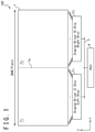
- FIG. 1 illustrates an example configuration of a display module 100 , according to one or more embodiments.
- the display module 100 is configured to display a frame image with a horizontal resolution of 3840 pixels.
- the display module 100 includes a display panel 1 and a display drivers 2 .
- the display panel 1 may be segmented into a plurality of display areas 3 such that the number of the display areas 3 is identical to the number of the display drivers 2 .
- the number of the display drivers 2 is two, and the two display drivers 2 have the same configuration.
- the display area 3 includes a left area 3 1 and a right area 3 2 , which are arrayed in the horizontal direction, which is indicated by the x axis of an xy coordinate system in FIG. 1 .
- the left area 3 1 and the right area 3 2 are located adjacent to each other at a boundary 1 a located at the center of the display panel 1 .
- a left half of a frame image may be displayed in the left area 3 1 and a right half of the frame image may be displayed in the right area 3 2 .
- the display drivers 2 include a left chip 2 1 configured to drive display elements disposed in the left area 3 1 of the display panel 1 and a right chip 2 2 configured to drive display elements disposed in the right area 3 2 .
- the left chip 2 1 and right chip 2 2 may be configured to support multidrop communication with a host 4 via a bus 5 .
- frame image data for the entirety of a frame image may be sent to both the left chip 2 1 and right chip 2 2 using the multidrop communication.
- the frame image data may include pixel data for respective pixels of the frame image.
- pixel data for each pixel may include grayscale values of respective colors (e.g., red, green, and blue).
- the left chip 2 1 is configured to drive display elements disposed in the left area 3 1 based on the frame image data received from the host 4
- the right chip 2 2 is configured to drive display elements disposed in the right area 3 2 based on the frame image data.
- FIG. 2 illustrates an exemplary pixel arrangement of the display panel 1 , according to one or more embodiments.
- a plurality of pixels 6 are arranged on the display panel 1 .
- Each pixel 6 may include a red (R) subpixel 7 R, a green (G) subpixel 7 G, and a blue (B) subpixel 7 B.
- the R subpixels 7 R, the G subpixels 7 G, and the B subpixels 7 B are indicated by “R”, “G”, and “B”, respectively.
- the R subpixels 7 R, the G subpixels 7 G, and the B subpixels 7 B may be hereinafter collectively referred to as subpixels 7 , if the colors of the subpixels 7 do not matter.
- the R subpixels 7 R, the G subpixels 7 G, and the B subpixels 7 B may include display elements configured to display red, green, and blue, respectively.
- each display element may include a light emitting element, a select transistor, and a storage capacitor.
- each display element may include a pixel electrode, a select transistor, and a storage capacitor.
- Each pixel 6 may additionally include one or more other subpixels 7 configured to display colors other than red, green, and blue.
- the display panel 1 is configured in a zigzag pixel arrangement.
- the display panel 1 may be configured such that pixels 6 in adjacent horizontal lines are shifted from each other. In the embodiment illustrated in FIG. 2 , pixels 6 in even-numbered horizontal lines are shifted leftward from pixels 6 in odd-numbered horizontal lines by one subpixel 7 .
- the shift amount and/or direction of the pixels 6 may be variously modified.
- pixels 6 in even-numbered horizontal lines may be shifted rightward from pixels 6 in odd-numbered horizontal lines by one subpixel 7 .
- the shift amount may be two subpixels 7 for both the cases of the leftward shift and the rightward shift.
- a subpixel 7 located near the boundary 1 a in the left area 3 1 may be driven based on pixel data for a pixel in a right half image area of the original frame image.
- R subpixels 7 R indicated by numerals “8” in even-numbered horizonal lines are driven based on grayscale values for red of pixel data for boundary pixels located in the right half image area of the original frame image, although they are actually located in the left area 3 1 .
- the boundary pixels may be located in contact with the boundary between the right half image area and the left half image area.
- a subpixel 7 located near the boundary 1 a in the right area 3 2 may be driven based on pixel data for a pixel in a left half image area of the original frame image.
- B subpixels 7 B indicated by numerals “9” in even-numbered horizonal lines are driven based on grayscale values for blue of pixel data for boundary pixels located in the left half image area of the original frame image, although they are actually located in the right area 3 2 .
- the boundary pixels may be located in contact with the boundary between the right half image area and the left half image area.
- FIG. 4 illustrates example configurations of the left chip 2 1 and the right chip 2 2 .
- the left chip 2 1 and the right chip 2 2 have the same configuration.
- a display driver 2 may be configured to operate as any of the left chip 2 1 and the right chip 2 2 .
- the display driver 2 is configured to operate as a left chip 2 1 in a left operation mode and operate as a right chip 2 2 in a right operation mode.
- the left chip 2 1 and the right chip 2 2 each include interface circuitry 11 , image data processing circuitry 12 , and drive circuitry 13 .
- the interface circuitry 11 may be configured to receive frame image data 31 from the host 4 and forward the same to the image data processing circuitry 12 .
- communications between the display drivers 2 and the host 4 may be achieved through low voltage differential signaling (LVDS), and the interface circuitry 11 may include an LVDS interface.
- the frame image data 31 received by the interface circuitry 11 and forwarded to the image data processing circuitry 12 during a vertical sync period may include pixel data for all the pixels of one frame image.
- the interface circuitry 11 may be configured to process frame image data received from the host 4 and use the processed frame image data as the frame image data 31 to be forwarded to the image data processing circuitry 12 .
- the frame image data 31 includes left image data 32 and right image data 33 .
- the left image data 32 may correspond to the left half image area of the frame image and include pixel data for pixels in the left half image area, where the pixel data may include grayscale values of the respective colors (e.g., red, green, and blue).
- the right image data 33 may correspond to the right half image area of the frame image and include grayscale values of the respective colors of pixels in the right half image area.
- Left image data 32 for one horizontal line may include pixel data for pixels for half the horizontal resolution of the frame image.
- left image data 32 for one horizontal line may include pixel data for 1920 pixels.
- Right image data 33 for one horizontal line may include pixel data for pixels for half the horizontal resolution of the frame image, correspondingly.
- right image data 33 for one horizontal line may include pixel data for 1920 pixels.
- the image data processing circuitry 12 is configured to generate, based on the frame image data 31 received from the interface circuitry 11 , display data 34 used to drive the display panel 1 by the drive circuitry 13 .
- numeral 34 1 denotes the display data 34 generated by the image data processing circuitry 12 of the left chip 2 1
- numeral 34 2 denotes the display data 34 generated by the image data processing circuitry 12 of the right chip 2 2 .
- the drive circuitry 13 of the left chip 2 1 is configured to drive the display elements in the left area 3 1 of the display panel 1 in response to the display data 34 1 received from the image data processing circuitry 12
- the drive circuitry 13 of the right chip 2 2 is configured to drive the display elements in the right area 3 2 of the display panel 1 in response to the display data 34 2 received from the image data processing circuitry 12 .
- the image data processing circuitry 12 may include a line memory (LM) 21 , a buffer memory (BM) 22 , an image processing (IP) core 23 , IP control circuitry 24 , and a line latch 25 .
- LM line memory
- BM buffer memory
- IP image processing
- the line memory 21 may be configured to store the frame image data 31 received from the interface circuitry 11 for one horizontal line.
- the line memory 21 may have a capacity to store pixel data for 3840 pixels.
- the buffer memory 22 is configured to sequentially receive and store the frame image data 31 from the line memory 21 .
- the buffer memory 22 may be configured to store the frame image data 31 for multiple horizontal lines. In the embodiment illustrated in FIG. 4 , the buffer memory 22 is configured to store the frame image data 31 for 68 horizontal lines.
- the buffer memory 22 may be configured to perform a first-in-first-out (FIFO) operation, outputting frame image data for the oldest horizontal line when newly receiving frame image data for one new horizontal line.
- FIFO first-in-first-out
- each of the left chip 2 1 and the right chip 2 2 may include a touch controller (not illustrated) for proximity sensing to sense an approach or contact of an input object to a touch panel.
- the number of horizontal lines for which the buffer memory 22 is configured to store the frame image data 31 may be selected to provide sufficient time for the touch controller to achieve the proximity sensing in each vertical sync period.
- the image processing IP core 23 is configured to process the frame image data 31 received from the buffer memory 22 to generate processed image data 35 .
- numeral 35 1 denotes the processed image data 35 generated by the image data processing circuitry 12 of the left chip 2 1
- numeral 35 2 denotes the processed image data 35 generated by the image data processing circuitry 12 of the right chip 2 2 .
- the processing performed by the image processing IP core 23 may be controlled by the IP control circuitry 24 .
- the processed image data 35 1 generated by the image processing IP core 23 of the left chip 2 1 include processed left image data 36 and processed right boundary image data 37 .
- the processed left image data 36 may be generated based on the left image data 32 of the frame image data 31 .
- the processed left image data 36 may be generated by applying desired image processing to the left image data 32 .
- the left image data 32 extracted from the frame image data 31 may be used as the processed left image data 36 without modification.
- the processed right boundary image data 37 may be generated based on pixel data of the right image data 33 for the pixels located in a portion of the right half image area of the frame image, the portion being in contact with the boundary between the left half image area and the right half image area.
- the processed right boundary image data 37 may be generated by extracting, from the right image data 33 , pixel data for pixels in the portion of the right half image area of the frame image, the portion being in contact with the boundary between the left half image area and the right half image area, and applying image processing to the extracted pixel data.
- the above-described pixel data extracted from the right image data 33 may be used as the processed right boundary image data 37 without modification.
- the processed image data 35 2 generated by the image processing IP core 23 of the right chip 2 2 includes processed right image data 38 and processed left boundary image data 39 .
- the processed right image data 38 may be generated based on the right image data 33 of the frame image data 31 .
- the processed right image data 38 may be generated by applying desired image processing to the right image data 33 .
- the right image data 33 extracted from the frame image data 31 may be used as the processed right image data 38 without modification.
- the processed left boundary image data 39 is generated based on pixel data of the left image data 32 for the pixels located in a portion of the left half image area of the frame image, the portion being in contact with the boundary between the left half image area and the right half image area.
- the processed left boundary image data 39 may be generated by extracting, from the left image data 32 , pixel data for pixels in the portion of the left half image area of the frame image, the portion being in contact with the boundary between the left half image area and the right half image area, and applying image processing to the extracted pixel data.
- the above-described pixel data extracted from the left image data 32 may be used as the processed left boundary image data 39 without modification.
- the line latches 25 may be configured to store the processed image data 35 for one horizontal line.
- the line latch 25 of the left chip 2 1 is configured to store the processed image data 35 1
- the line latch 25 of the right chip 2 2 is configured to store the processed image data 35 2 .
- the line latches 25 are adapted to data transfer to the drive circuitry 13 .
- data sorting is performed during the data transfer from the line latches 25 to the drive circuitry 13 to generate and supply display data 34 to the drive circuitry 13 .
- the data sorting may be performed in accordance with the arrangement of the pixels 6 of the display panel 1 .
- part of the processed image data 35 1 stored in the line latch 25 of the left chip 2 1 and used to drive the display elements in the left area 3 1 is selected in accordance with the arrangement of the pixels 6 of the display panel 1 , and the selected part of the processed image data 35 1 is transferred to the drive circuitry 13 .
- the part of the processed image data 35 1 thus transferred to the drive circuitry 13 is used as the display data 34 1 .
- part of the processed image data 35 2 stored in the line latch 25 of the right chip 2 2 is correspondingly selected in accordance with the arrangement of the pixels 6 of the display panel 1 , and the selected part to of the processed image data 35 2 is transferred to the drive circuitry 13 .
- the part of the processed image data 35 2 thus transferred to the drive circuitry 13 is used as the display data 34 2 .
- the processed image data 35 1 generated in the left chip 2 1 includes the processed right boundary image data 37 for all the horizontal lines of the frame image
- the processed image data 35 2 generated in the right chip 2 2 includes the processed left boundary image data 39 for all the horizontal lines of the frame image.
- FIG. 5 illustrates an example configuration of display drivers 2 (including the left chip 2 1 and the right chip 2 2 ), according to other embodiments.
- image data processing circuitry 12 A of each display driver 2 includes data extraction circuitry 41 , a line memory 42 , a buffer memory 43 , an image processing IP core 44 , IP control circuitry 45 and a line latch 46 .
- frame image data 31 received by the interface circuitry 11 during each vertical sync period include pixel data for all the pixels of one frame image
- the data extraction circuitry 41 is configured to extract pixel data to be stored in the line memory 42 and the buffer memory 43 from the frame image data 31 received from the interface circuitry 11 .
- the extracted pixel data may be forwarded to the line memory 42 .
- the data extraction circuitry 41 of the left chip 2 1 is configured to extract left image data 32 and right boundary image data 51 from the frame image data 31 received from the interface circuitry 11 .
- the left image data 32 may correspond to the left half image area of the frame image and include grayscale values of the respective colors (e.g., red, green, and blue) of pixels in the left half image area.
- the right boundary image data 51 may include pixel data for pixels located in a portion of the right half image area of the frame image, the portion being in contact with the boundary between the left half image area and the right half image area.
- the extracted left image data 32 and the right boundary image data 51 may be forwarded to the line memory 42 of the left chip 2 1 .
- the data extraction circuitry 41 of the right chip 2 2 is configured to extract right image data 33 and left boundary image data 52 from the frame image data 31 received from the interface circuitry 11 .
- the right image data 33 may correspond to the right half image area of the frame image and include grayscale values of the respective colors of pixels in the right half image area.
- the left boundary image data 52 may include pixel data for pixels located in a portion of the left half image area of the frame image, the portion being in contact with the boundary between the left half image area and the right half image area.
- the extracted right image data 33 and the left boundary image data 52 may be forwarded to the line memory 42 of the right chip 2 2 .
- the right and left boundary image data 51 and 52 for one horizontal line may include pixel data for a number of pixels, the number being determined in accordance with image processing performed in the image processing IP cores 44 .
- the image processing IP cores 44 are each configured to perform image processing in units of blocks each consisting of a pixels located in the same horizontal line where a is a natural number of two or more, and the right and left boundary image data 51 and 52 for one horizontal line may each include pixel data for a pixels of one block.
- FIG. 5 illustrates the case where one block consists of eight pixels.
- the line memory 42 of the left chip 2 1 is configured to sequentially store the left image data 32 and the right boundary image data 51 received from the corresponding data extraction circuitry 41 and sequentially forward the same to the corresponding buffer memory 43 .
- the line memory 42 of the right chip 2 2 is configured to sequentially store the right image data 33 and the left boundary image data 52 received from the corresponding data extraction circuitry 41 and sequentially forward the same to the corresponding buffer memory 43 .
- FIG. 6 illustrates an example operation of the data extraction circuitry 41 , according to one or more embodiments.
- pixel data of the frame image data 31 are sequentially transmitted to the interface circuitry 11 of the left and right chips 2 1 and 2 2 from the host 4 .
- pixel data of the i th pixel of the frame image from the left is indicated by “#i.”
- the horizonal resolution of the frame image is 3840 pixels, for example, pixel data #1 to #1920 of the left image data 32 are first sequentially transmitted to the interface circuitry 11 , and then pixel data #1921 to #3840 of the right image data 33 are sequentially transmitted to the interface circuitry 11 .
- the data extraction circuitry 41 of the left chip 2 1 is configured to extract pixel data #1 to #1920 as the left image data 32 and further extract pixel data #1921 to #1928 as the right boundary image data 51 .
- the illustrated embodiment corresponds to the case where the image processing IP core 44 is configured to perform image processing in units of blocks each consisting of eight pixels located in the same horizontal line.
- the extracted left image data 32 and the right boundary image data 51 may be forwarded and stored in the line memory 42 .
- the left image data 32 and the right boundary image data 51 stored in the line memory 42 may be forwarded to the buffer memory 43 in the next horizontal sync period.
- the data extraction circuitry 41 of the right chip 2 2 is configured to extract pixel data #1913 to #1920 as the left boundary image data 52 and further extract pixel data #1921 to #3840 as the right image data 33 .
- the extracted left boundary image data 52 and the right image data 33 may be forwarded and stored in the line memory 42 .
- the left boundary image data 52 and the right image data 33 stored in the line memory 42 may be forwarded to the buffer memory 43 in the next horizontal sync period.
- the operation of the data extraction circuitry 41 illustrated in FIG. 6 enables driving the display panel 1 configured in the zigzag pixel arrangement, while contributing reduction in the capacities of the line memories 42 and the buffer memories 43 .
- the image processing IP core 44 of the left chip 2 1 may be configured to receive the left image data 32 and right boundary image data 51 from the buffer memory 43 and generate the processed image data 35 1 based on the received left image data 32 and right boundary image data 51 .
- the processed image data 35 1 may include processed left image data 36 and processed right boundary image data 37 .
- the processed left image data 36 may be generated based on the left image data 32 of the frame image data 31
- the processed right boundary image data 37 may be generated based on the right boundary image data 51 .
- the processed left image data 36 is generated by applying desired image processing to the left image data 32 .
- the left image data 32 may be used as the processed left image data 36 without modification.
- the processed right boundary image data 37 may be generated based on the right boundary image data 51 .
- the processed right boundary image data 37 may be generated by applying image processing to the right boundary image data 51 .
- the right boundary image data 51 may be used as the processed right boundary image data 37 without modification.
- the image processing IP core 44 of the right chip 2 2 may be configured to receive the right image data 33 and left boundary image data 52 and generate the processed image data 35 2 based on the received right image data 33 and left boundary image data 52 .
- the processed image data 35 2 may include processed right image data 38 and processed left boundary image data 39 .
- the processed right image data 38 may be generated based on the right image data 33 of the frame image data 31
- the processed left boundary image data 39 may be generated based on the left boundary image data 52 .
- the processed right image data 38 is generated by applying desired image processing to the right image data 33 .
- the right image data 33 may be used as the processed right image data 38 without modification.
- the processed left boundary image data 39 may be generated based on the left boundary image data 52 .
- the processed left boundary image data 39 may be generated by applying image processing to the left boundary image data 52 .
- the left boundary image data 52 may be used as the processed left boundary image data 39 without modification.
- the image processing IP cores 44 of the left and right chips 2 1 and 2 2 are configured to exchange control data used for the image processing.
- the image processing IP core 44 of the left chip 2 1 may be configured to calculate a feature value of the left image area of the frame image (e.g., the average picture level (APL) of the left image area) based on the left image data 32 and send the calculated feature value to the image processing IP core 44 of the right chip 2 2 .
- APL average picture level
- the image processing IP core 44 of the right chip 2 2 may be configured to calculate a feature value of the right image area of the frame image (e.g., the average picture level (APL) of the right image area) based on the right image data 33 and send the calculated feature value to the image processing IP core 44 of the left chip 2 1 .
- the image processing IP core 44 of the left chip 2 1 may be configured to calculate a feature value of the entire frame image based on the feature value calculated by itself and the feature value calculated by the right chip 2 2 and perform the image processing based on the calculated feature value of the entire frame image.
- the image processing IP core 44 of the right chip 2 2 may be configured to calculate a feature value of the entire frame image based on the feature value calculated by itself and the feature value calculated by the left chip 2 1 and perform the image processing based on the calculated feature value of the entire frame image. This operation enables the image processing IP cores 44 of both the left and right chips 2 1 and 2 2 to perform the image processing based on the feature value of the entire frame image (e.g., the APL of the entire frame image).
- the processed image data 35 1 and 35 2 are subjected to data transfer similar to the embodiment described in relation to FIG. 4 to supply the display data 34 1 and 34 2 to the drive circuitry 13 .
- data sorting is performed during this data transfer in accordance with the arrangement of the pixels 6 of the display panel 1 .
- the drive circuitry 13 of the left chip 2 1 may be configured to drive the display elements in the left area 3 1 of the display panel 1 based on the display data 34 1 received from the corresponding image processing circuitry 12
- the drive circuitry 13 of the right chip 2 2 may be configured to drive the display elements in the right area 3 2 of the display panel 1 based on the display data 34 2 received from the corresponding image processing circuitry 12 .
- a display driver 2 is configured to operate as the left chip 2 1 illustrated in FIG. 5 when placed in a left operation mode and operate as the right chip 2 2 when placed in a right operation mode.
- FIG. 7 is a flowchart illustrating method 700 in accordance with one or more embodiments.
- Method 700 may be executed by the display drivers 2 .
- one or more of the steps illustrated in FIG. 7 may be omitted, repeated, and/or performed in a different order than the order shown in FIG. 7 .
- first and second display drivers 2 receive first frame image data for a first frame image (e.g., the frame image data 31 .)
- the first display driver 2 e.g., the left chip 2 1
- the first image area image data includes pixel data for pixels in a first image area (e.g., the left area 3 1 ) of the display panel 1 .
- the first image area image data may be or may include the left image data 32 defined for the left area 3 1 .
- the first boundary image data includes pixel data for boundary pixels located in a first portion of a second image area (e.g., the right area 3 2 ) of the first frame image, where the second image area is adjacent to the first image area, and the first portion is located in contact with the boundary between the first image area and the second image area.
- the first boundary image data may be or may include the right boundary image data 51 .
- the second display driver 2 extracts second image area image data and second boundary image data from the first frame image data.
- the second image area image data includes pixel data for pixels in a second image area (e.g., the right area 3 2 ) of the display panel 1 .
- the second image area image data may be or may include the right image data 33 defined for the right area 3 2 .
- the second boundary image data includes pixel data for boundary pixels located in a second portion of the first image area (e.g., the left area 3 1 ) of the first frame image, where the second portion is located in contact with the boundary between the first image area and the second image area.
- the first image area is the left area 3 1
- the second boundary image data may be or may include the left boundary image data 52 .
- the first display driver 2 generates first display data (e.g., the display data 34 1 ) based on the first image area image data and the first boundary image data.
- the first display driver 2 may generate processed first image area data (e.g., the processed left image data 36 ) and processed first boundary image data (e.g., the processed right boundary image data 37 ) by applying image processing to the first image area image data and the first boundary image data, respectively.
- the first display driver 2 may further generate the first display data based on the processed first image area data and the processed first boundary image data.
- the generation of the first display data may include data sorting or selection of the processed first image area data and the processed first boundary image data for each horizontal line.
- the second display driver 2 generate second display data (e.g., the display data 34 2 ) based on the second image area image data and the second boundary image data.
- the second display driver 2 may generate processed second image area data (e.g., the processed right image data 38 ) and processed second boundary image data (e.g., the processed left boundary image data 39 ) by applying image processing to the second image area image data and the second boundary image data, respectively.
- the second display driver 2 may further generate the second display data based on the processed second image area data and the processed second boundary image data.
- the generation of the second display data may include data sorting or selection of the processed second image area data and the processed second boundary image data for each horizontal line.
- the first display driver 2 drives display elements in a first display area (e.g., the left area 3 1 ) of the display panel 1 based on the first display data.
- the second display driver 2 drives display elements in a second display area (e.g., the right area 3 2 ) of the display panel 1 based on the second display data.
- the display driver 2 may further have an independent operation mode to drive a display panel 1 A that has a horizontal resolution of one-half of the resolution of the display panel 1 illustrated in FIG. 1 .
- the display driver 2 can independently drive the display panel 1 A in a display module 100 A.
- FIG. 9 illustrates an example operation of the display driver 2 in the independent operation mode.
- the data extraction circuitry 41 stops operating, and the interface circuitry 11 sequentially forwards frame image data 53 received from the host 4 to the line memory 42 without modification.
- the frame image data 53 forwarded to the line memory 42 may be further forwarded and stored in the buffer memory 43 .
- the image processing IP core 44 may receive the frame image data 53 from the buffer memory 43 and generate processed image data 54 by applying image processing to the received frame image data 53 .
- the processed image data 54 may be forwarded to the line latch 46 and further to the drive circuitry 13 .
- the drive circuitry 13 may drive the display elements of the display panel 1 A based on the processed image data 54 .
- the number of pixels for which pixel data are stored in the buffer memory 43 per horizontal line is reduced less than that for the case when the display driver 2 is placed in the left operation mode or the right operation mode.
- the number of horizontal lines for which pixel data are stored in the buffer memory 43 is increased when the display driver IC chip 2 is placed in the independent operation mode. This operation is useful, for example, when a touch controller (not illustrated) is integrated in the display driver 2 . Storing pixel data for an increased number of horizontal lines in the buffer memory 43 is useful for providing sufficient time for achieving proximity sensing by the touch controller in each vertical sync period.
- left image data 32 and right boundary image data 51 for p horizontal lines may be stored in the buffer memory 43 , where p is a natural number of two or more. In the embodiment illustrated in FIG. 5 , p is 66. In various embodiments, p may be determined based on the capacity of the buffer memory 43 and/or the horizontal resolution. In embodiments where the left image data 32 for one horizontal line includes pixel data for 1920 pixels and the right boundary image data 51 for one horizontal line includes pixel data for eight pixels, the number of pixels for which the buffer memory 43 stores pixel data per horizontal line is 1928 in the left operation mode.
- right image data 33 and left boundary image data 52 for p horizontal lines may be stored in the buffer memory 43 .
- the number of pixels for which the buffer memory 43 stores pixel data per horizontal line is 1928 also in the right operation mode.
- frame image data 53 for q horizontal lines may be stored in the buffer memory 43 , where q is a natural number larger than p. In the embodiment illustrated in FIG. 9 , q is 68. In embodiments where the frame image data 53 for one horizontal line includes pixel data for 1920 pixels, the number of pixels for which the buffer memory 43 stores pixel data per horizontal line is 1920 in the independent operation mode.
- FIG. 10 illustrates an example configuration of a display module 100 B, according to other embodiments.
- the display module 100 B includes a display panel 1 segmented into three display areas 3 arrayed in the horizontal direction and three display drivers 2 configured to drive the three display areas 3 , respectively.
- the three display area 3 may include a left area 3 1 , a right area 3 2 , and a middle area 3 3 .
- the left area 3 1 and the middle area 3 3 are adjacent across the boundary 1 b
- the middle area 3 3 and the right area 3 2 are adjacent across the boundary 1 c .
- the three DDIC 2 includes a left chip 2 1 configured to drive the left area 3 1 , a right chip 2 2 configured to drive the right area 3 2 , and a middle chip 2 3 configured to drive the middle area 3 3 .
- the left chip 2 1 , the right chip 2 2 , and the middle chip 2 3 may have the same configuration.
- Each display driver 2 may be configured to operate as the left chip 2 1 , the right chip 2 2 , and the middle chip 2 3 , when placed in a left operation mode, a right operation mode, and a middle operation mode, respectively.
- FIG. 11 illustrates an example configuration of the display drivers 2 of the display module 100 B, according to one or more embodiments.
- the image data processing circuitry 12 A of each of the left chip 2 1 , the right chip 2 2 , and the middle chip 2 3 includes data extraction circuitry 41 A, a line memory 42 , a buffer memory 43 , an image processing IP core 44 , and a line latch 46 .
- frame image data 61 received by the interface circuitry 11 of each display driver 2 during each vertical sync period includes pixel data for all the pixels of one frame image
- the data extraction circuitry 41 A is configured to extract pixel data to be stored in the line memory 42 and the buffer memory 43 from the frame image data 61 received from the interface circuitry 11 .
- the extracted pixel data may be forwarded to the line memory 42 .
- the frame image data 61 may include left image data 62 (which may be also referred to as first image area image data), right image data 63 (which may be also referred to as second image area image data), and middle image data 64 (which may be also referred to as second image area image data).
- the left image data 62 may be associated with or defined for the left image area (which may be also referred to as first image area) of the frame image and include pixel data for respective pixels in the left image area.
- the right image data 63 may be associated with or defined for a right image area (which may be also referred to as second image area) of the frame image and include grayscale values of respective colors of respective pixels in the right image area.
- the middle image data 64 may be associated with or defined for a middle image area (which may be also referred to as third image area) of the frame image and include grayscale values of respective colors of respective pixels in the middle image area.
- Left image data 62 for one horizontal line may include pixel data for a number of pixels, the number being one-third of the horizontal resolution of the frame image.
- the horizontal resolution of the frame image is 3840 pixels
- the left image data 62 for one horizontal line includes pixel data for 1280 pixels.
- right image data 63 and middle image data 64 for one horizontal line may each include pixel data for a number of pixels, the number being one-third of the horizontal resolution of the frame image.
- the right image data 63 and the middle image data 64 for one horizontal line include pixel data for 1280 pixels.
- the data extraction circuitry 41 A of the left chip 2 1 may be configured to extract the left image data 62 and first right boundary image data 65 from the frame image data 61 received from the interface circuitry 11 .
- the first right boundary image data 65 may include pixel data for pixels located in a portion of the middle image area of the frame image, the portion being adjacent to the left image area.
- the left image data 62 and first right boundary image data 65 thus extracted may be forwarded to the line memory 42 in the left chip 2 1 .
- the data extraction circuitry 41 A of the right chip 2 2 may be configured to extract the right image data 63 and first left boundary image data 66 from the frame image data 61 received from the interface circuitry 11 .
- the first left boundary image data 66 may include pixel data for pixels located in a portion of the middle image area of the frame image, the portion being adjacent to the right image area.
- the right image data 63 and first left boundary image data 66 thus extracted may be forwarded to the line memory 42 in the right chip 2 2 .
- the data extraction circuitry 41 A of the middle chip 2 3 may be configured to extract the middle image data 64 , second left boundary image data 67 , and second right boundary image data 68 from the frame image data 61 received from the interface circuitry 11 .
- the second left boundary image data 67 may include pixel data for pixels located in a portion of the left image area of the frame image, the portion being adjacent to the middle image area.
- the second right boundary image data 68 may include pixel data for pixels located in a portion of the right image area of the frame image, the portion being adjacent to the middle image area.
- the middle image data 64 , second left boundary image data 67 and second right boundary image data 68 thus extracted may be forwarded to the line memory 42 in the middle chip 2 3 .
- Such operation of the data extraction circuitry 41 A enables driving the display panel 1 configured in the zigzag pixel arrangement, while contributing reduction in the capacities of the line memories 42 and the buffer memories 43 .
- the first right boundary image data 65 , the first left boundary image data 66 , the second left boundary image data 67 , and the second right boundary image data 68 for one horizontal line may each include pixel data for a number of pixels, the number being determined based on image processing performed in the image processing IP cores 44 .
- the image processing IP cores 44 are each configured to perform image processing in units of blocks each consisting of a pixels located in the same horizontal line where a is a natural number of two or more
- the first right boundary image data 65 , the first left boundary image data 66 , the second left boundary image data 67 , and the second right boundary image data 68 for one horizontal line may each include pixel data for a pixels of one block.
- FIG. 10 illustrates the case where one block consists of eight pixels.
- the line memory 42 of the left chip 2 1 is configured to sequentially store the left image data 62 and the first right boundary image data 65 received from the corresponding data extraction circuitry 41 A and sequentially forward the same to the corresponding buffer memory 43 .
- the line memory 42 of the right chip 2 2 is configured to sequentially store the right image data 63 and the first left boundary image data 66 received from the corresponding data extraction circuitry 41 A and sequentially forward the same to the corresponding buffer memory 43 .
- the line memory 42 of the middle chip 2 3 is configured to sequentially store the middle image data 64 , the second left boundary image data 67 , and the second right boundary image data 68 received from the corresponding data extraction circuitry 41 A and sequentially forward the same to the corresponding buffer memory 43 .
- the image processing IP core 44 of the left chip 2 1 may be configured to generate processed image data 69 1 by applying desired processing to the left image data 62 and the first right boundary image data 65 received from the corresponding buffer memory 43 .
- the processed image data 69 1 may include processed left image data 71 and first processed right boundary image data 72 .
- the image processing IP core 44 of the left chip 2 1 may be configured to generate the processed left image data 71 and the first processed right boundary image data 72 by applying desired image processing to the left image data 62 and the first right boundary image data 65 , respectively.
- the processed image data 69 1 thus generated may be forwarded to the line latch 46 of the left chip 2 1 .
- the image processing IP core 44 of the right chip 2 2 may be configured to generate processed image data 69 2 by applying desired processing to the right image data 63 and the first left boundary image data 66 received from the corresponding buffer memory 43 .
- the processed image data 69 2 may include processed right image data 73 and first processed left boundary image data 74 .
- the image processing IP core 44 of the right chip 2 2 may be configured to generate the processed right image data 73 and the first processed left boundary image data 74 by applying desired image processing to the right image data 63 and the first left boundary image data 66 , respectively.
- the processed image data 69 2 thus generated may be forwarded to the line latch 46 in the right chip 2 2 .
- the image processing IP core 44 of the middle chip 2 3 may be configured to generate processed image data 69 3 by applying desired processing to the middle image data 64 , the second left boundary image data 67 , and the second right boundary image data 68 received from the buffer memory 43 .
- the processed image data 69 3 may include processed middle image data 75 , second processed left boundary image data 76 , and second processed right boundary image data 77 .
- the image processing IP core 44 of the middle chip 2 3 may be configured to generate the processed middle image data 75 , the second processed left boundary image data 76 , and the second processed right boundary image data 77 by applying desired image processing to the middle image data 64 , the second left boundary image data 67 , and the second right boundary image data 68 , respectively.
- the processed image data 69 3 thus generated may be forwarded to the line latch 46 of the middle chip 2 3 .
- the line latch 46 of each display driver 2 is adapted to data transfer to the corresponding drive circuitry 13 .
- data sorting is performed during the data transfer from the line latch 46 to the drive circuitry 13 to thereby supply display data 70 to the drive circuitry 13 .
- the data sorting may be performed in accordance with the arrangement of the pixels 6 in the display panel 1 .
- display data used to drive the display elements in the left area 3 1 may be selected from the processed image data 69 1 stored in the line latch 46 of the left chip 2 1 and transferred to the corresponding drive circuitry 13 .
- the data transferred to the drive circuitry 13 of the left chip 2 1 may be used as the display data 70 1 .
- display data used to drive the display elements in the right area 3 2 may be selected from the processed image data 69 2 stored in the line latch 46 of the right chip 2 2 and transferred to the corresponding drive circuitry 13 .
- the data transferred to the drive circuitry 13 of the right chip 2 2 may be used as the display data 70 2 .
- display data used to drive the display elements in the middle area 3 3 may be selected from the processed image data 69 3 stored in the line latch 46 of the middle chip 2 3 and transferred to the corresponding drive circuitry 13 .
- the data transferred to the drive circuitry 13 of the middle chip 2 3 may be used as the display data 70 3 .
- the drive circuitry 13 of the left chip 2 1 is configured to drive the display elements in the left area 3 1 of the display panel 1 based on the display data 70 1 ;
- the drive circuitry 13 of the right chip 2 2 is configured to drive the display elements in the right area 3 2 of the display panel 1 based on the display data 70 2 ;
- the drive circuitry 13 of the middle chip 2 3 is configured to drive the display elements in the middle area 3 3 of the display panel 1 based on the display data 70 3 .
- the display panel 1 may be segmented into M display areas 3 and driven with M display drivers 2 , where M is a natural number of three or more.
- the display driver 2 that drives the leftmost one of the M display areas 3 may be configured to operate similarly to the left chip 2 1 described in relation to FIG. 10
- the display driver 2 that drives the rightmost one of the M display areas 3 may be configured to operate similarly to the right chip 2 2 described in relation to FIG. 10
- the (M-2) display drivers 2 that drives the middle display area(s) 3 may be configured to operate similarly to the middle chip 2 3 described in relation to FIG. 10 .
Abstract
Description
Claims (20)
Applications Claiming Priority (3)
| Application Number | Priority Date | Filing Date | Title |
|---|---|---|---|
| JP2019-137636 | 2019-07-26 | ||
| JP2019137636A JP7407535B2 (en) | 2019-07-26 | 2019-07-26 | Display driver IC chip, display module, and display panel driving method |
| JPJP2019-137636 | 2019-07-26 |
Publications (2)
| Publication Number | Publication Date |
|---|---|
| US20210027741A1 US20210027741A1 (en) | 2021-01-28 |
| US11227563B2 true US11227563B2 (en) | 2022-01-18 |
Family
ID=74187675
Family Applications (1)
| Application Number | Title | Priority Date | Filing Date |
|---|---|---|---|
| US16/909,758 Active US11227563B2 (en) | 2019-07-26 | 2020-06-23 | Device and method for driving a display panel |
Country Status (2)
| Country | Link |
|---|---|
| US (1) | US11227563B2 (en) |
| JP (1) | JP7407535B2 (en) |
Citations (5)
| Publication number | Priority date | Publication date | Assignee | Title |
|---|---|---|---|---|
| US20060256033A1 (en) * | 2005-05-13 | 2006-11-16 | Chan Victor G | Method and apparatus for displaying an image on at least two display panels |
| US20090189848A1 (en) * | 2008-01-24 | 2009-07-30 | Seiko Epson Corporation | Method of driving electrophoretic display device, electrophotetic display device, and electronic apparatus |
| US20120194572A1 (en) * | 2009-08-27 | 2012-08-02 | Sharp Kabushiki Kaisha | Display device |
| US20190198575A1 (en) * | 2017-12-22 | 2019-06-27 | Au Optronics Corporation | Display device |
| US20190347985A1 (en) * | 2018-05-09 | 2019-11-14 | Apple Inc. | Local passive matrix display |
Family Cites Families (6)
| Publication number | Priority date | Publication date | Assignee | Title |
|---|---|---|---|---|
| JPH04326323A (en) * | 1991-04-26 | 1992-11-16 | Hitachi Ltd | Display controller |
| JP3451298B2 (en) * | 1995-03-08 | 2003-09-29 | カシオ計算機株式会社 | Liquid crystal display |
| JPH1145076A (en) * | 1997-07-24 | 1999-02-16 | Semiconductor Energy Lab Co Ltd | Active matrix type display device |
| JP6114530B2 (en) * | 2012-10-16 | 2017-04-12 | ルネサスエレクトロニクス株式会社 | Display device and display device driver |
| KR102141542B1 (en) * | 2013-12-31 | 2020-09-14 | 엘지디스플레이 주식회사 | Display device |
| JP2015210324A (en) * | 2014-04-24 | 2015-11-24 | 株式会社ジャパンディスプレイ | Display device and method of driving the same |
-
2019
- 2019-07-26 JP JP2019137636A patent/JP7407535B2/en active Active
-
2020
- 2020-06-23 US US16/909,758 patent/US11227563B2/en active Active
Patent Citations (5)
| Publication number | Priority date | Publication date | Assignee | Title |
|---|---|---|---|---|
| US20060256033A1 (en) * | 2005-05-13 | 2006-11-16 | Chan Victor G | Method and apparatus for displaying an image on at least two display panels |
| US20090189848A1 (en) * | 2008-01-24 | 2009-07-30 | Seiko Epson Corporation | Method of driving electrophoretic display device, electrophotetic display device, and electronic apparatus |
| US20120194572A1 (en) * | 2009-08-27 | 2012-08-02 | Sharp Kabushiki Kaisha | Display device |
| US20190198575A1 (en) * | 2017-12-22 | 2019-06-27 | Au Optronics Corporation | Display device |
| US20190347985A1 (en) * | 2018-05-09 | 2019-11-14 | Apple Inc. | Local passive matrix display |
Also Published As
| Publication number | Publication date |
|---|---|
| JP7407535B2 (en) | 2024-01-04 |
| US20210027741A1 (en) | 2021-01-28 |
| JP2021021814A (en) | 2021-02-18 |
Similar Documents
| Publication | Publication Date | Title |
|---|---|---|
| KR102512990B1 (en) | Display driving circuit and display device comprising thereof | |
| US9330592B2 (en) | Pixel structure and display device comprising the same | |
| KR101385225B1 (en) | Liquid crystal display and method for driving the same | |
| CN104505038B (en) | The drive circuit and liquid crystal display device of a kind of liquid crystal panel | |
| US9837009B2 (en) | Apparatus and method for driving display panel | |
| US10504412B2 (en) | Display apparatus and driving method thereof | |
| JP2011242744A (en) | Image processing method and display device using the same | |
| US9729866B2 (en) | Method of displaying a stereoscopic image and display device | |
| CN106847196B (en) | Circuit device, electro-optical device, and electronic apparatus | |
| EP3690870A1 (en) | Display driving method based on integrated circuit, integrated circuit, display screen, and display device | |
| US20160125843A1 (en) | Display driver ic and electronic device including the same | |
| CN102593151A (en) | Pixel structure, driving method thereof and self-luminous display using same | |
| CN104778927A (en) | Liquid crystal display device adapted to partial display | |
| CN101488312B (en) | Scan driver, flat panel display using the same and associated methods | |
| US10475406B2 (en) | Display panel having zigzag connection structure and display device including the same | |
| US11227563B2 (en) | Device and method for driving a display panel | |
| CN105448254B (en) | LCD device and for construct repair categorical data format structure method | |
| US10262624B2 (en) | Separating a compressed stream into multiple streams | |
| US8120573B2 (en) | Color sequential timing controlling circuit and both color sequential display system and method thereof | |
| WO2018099235A1 (en) | Display assembly, display device and display control method | |
| CN104575414B (en) | Display driver | |
| JP4614261B2 (en) | Controller driver and operation method thereof | |
| US8487854B2 (en) | Liquid crystal display device and driving method thereof | |
| CN112086051A (en) | Gamma correction circuit, gamma correction method and display device | |
| KR102306985B1 (en) | Display device |
Legal Events
| Date | Code | Title | Description |
|---|---|---|---|
| FEPP | Fee payment procedure |
Free format text: ENTITY STATUS SET TO UNDISCOUNTED (ORIGINAL EVENT CODE: BIG.); ENTITY STATUS OF PATENT OWNER: LARGE ENTITY |
|
| AS | Assignment |
Owner name: SYNAPTICS INCORPORATED, CALIFORNIA Free format text: ASSIGNMENT OF ASSIGNORS INTEREST;ASSIGNORS:SUZUKI, KENTARO;OTA, SHIGERU;IWASAKI, YOSHITAKA;REEL/FRAME:053300/0259 Effective date: 20200626 |
|
| STPP | Information on status: patent application and granting procedure in general |
Free format text: DOCKETED NEW CASE - READY FOR EXAMINATION |
|
| AS | Assignment |
Owner name: WELLS FARGO BANK, NATIONAL ASSOCIATION, NORTH CAROLINA Free format text: SECURITY INTEREST;ASSIGNOR:SYNAPTICS INCORPORATED;REEL/FRAME:055581/0737 Effective date: 20210311 |
|
| STPP | Information on status: patent application and granting procedure in general |
Free format text: NON FINAL ACTION MAILED |
|
| STPP | Information on status: patent application and granting procedure in general |
Free format text: RESPONSE TO NON-FINAL OFFICE ACTION ENTERED AND FORWARDED TO EXAMINER |
|
| STPP | Information on status: patent application and granting procedure in general |
Free format text: FINAL REJECTION MAILED |
|
| STPP | Information on status: patent application and granting procedure in general |
Free format text: RESPONSE AFTER FINAL ACTION FORWARDED TO EXAMINER |
|
| STPP | Information on status: patent application and granting procedure in general |
Free format text: NOTICE OF ALLOWANCE MAILED -- APPLICATION RECEIVED IN OFFICE OF PUBLICATIONS |
|
| STPP | Information on status: patent application and granting procedure in general |
Free format text: PUBLICATIONS -- ISSUE FEE PAYMENT VERIFIED |
|
| STCF | Information on status: patent grant |
Free format text: PATENTED CASE |