US11224927B2 - Circuit card attachment for enhanced robustness of thermal performance - Google Patents
Circuit card attachment for enhanced robustness of thermal performance Download PDFInfo
- Publication number
- US11224927B2 US11224927B2 US14/951,770 US201514951770A US11224927B2 US 11224927 B2 US11224927 B2 US 11224927B2 US 201514951770 A US201514951770 A US 201514951770A US 11224927 B2 US11224927 B2 US 11224927B2
- Authority
- US
- United States
- Prior art keywords
- circuit card
- printed circuit
- cooling
- temperature
- semiconductor device
- Prior art date
- Legal status (The legal status is an assumption and is not a legal conclusion. Google has not performed a legal analysis and makes no representation as to the accuracy of the status listed.)
- Active, expires
Links
Images


Classifications
-
- B—PERFORMING OPERATIONS; TRANSPORTING
- B23—MACHINE TOOLS; METAL-WORKING NOT OTHERWISE PROVIDED FOR
- B23K—SOLDERING OR UNSOLDERING; WELDING; CLADDING OR PLATING BY SOLDERING OR WELDING; CUTTING BY APPLYING HEAT LOCALLY, e.g. FLAME CUTTING; WORKING BY LASER BEAM
- B23K1/00—Soldering, e.g. brazing, or unsoldering
- B23K1/0008—Soldering, e.g. brazing, or unsoldering specially adapted for particular articles or work
- B23K1/0016—Soldering of electronic components
-
- B—PERFORMING OPERATIONS; TRANSPORTING
- B23—MACHINE TOOLS; METAL-WORKING NOT OTHERWISE PROVIDED FOR
- B23K—SOLDERING OR UNSOLDERING; WELDING; CLADDING OR PLATING BY SOLDERING OR WELDING; CUTTING BY APPLYING HEAT LOCALLY, e.g. FLAME CUTTING; WORKING BY LASER BEAM
- B23K1/00—Soldering, e.g. brazing, or unsoldering
- B23K1/008—Soldering within a furnace
-
- H—ELECTRICITY
- H05—ELECTRIC TECHNIQUES NOT OTHERWISE PROVIDED FOR
- H05K—PRINTED CIRCUITS; CASINGS OR CONSTRUCTIONAL DETAILS OF ELECTRIC APPARATUS; MANUFACTURE OF ASSEMBLAGES OF ELECTRICAL COMPONENTS
- H05K3/00—Apparatus or processes for manufacturing printed circuits
- H05K3/30—Assembling printed circuits with electric components, e.g. with resistors
- H05K3/32—Assembling printed circuits with electric components, e.g. with resistors electrically connecting electric components or wires to printed circuits
- H05K3/34—Assembling printed circuits with electric components, e.g. with resistors electrically connecting electric components or wires to printed circuits by soldering
- H05K3/3494—Heating processes for reflow soldering
-
- B—PERFORMING OPERATIONS; TRANSPORTING
- B23—MACHINE TOOLS; METAL-WORKING NOT OTHERWISE PROVIDED FOR
- B23K—SOLDERING OR UNSOLDERING; WELDING; CLADDING OR PLATING BY SOLDERING OR WELDING; CUTTING BY APPLYING HEAT LOCALLY, e.g. FLAME CUTTING; WORKING BY LASER BEAM
- B23K2101/00—Articles made by soldering, welding or cutting
- B23K2101/36—Electric or electronic devices
- B23K2101/42—Printed circuits
-
- H01L2224/131—
-
- H01L2224/16227—
-
- H01L2224/16245—
-
- H01L2224/2919—
-
- H01L2224/32225—
-
- H01L2224/32245—
-
- H01L2224/33181—
-
- H01L2224/73204—
-
- H01L2224/73253—
-
- H01L24/13—
-
- H01L24/16—
-
- H01L24/29—
-
- H01L24/32—
-
- H01L2924/00—
-
- H01L2924/00014—
-
- H01L2924/0103—
-
- H01L2924/01047—
-
- H01L2924/0105—
-
- H01L2924/014—
-
- H01L2924/15311—
-
- H01L2924/15724—
-
- H01L2924/15738—
-
- H01L2924/15747—
-
- H01L2924/16251—
-
- H01L2924/163—
-
- H—ELECTRICITY
- H05—ELECTRIC TECHNIQUES NOT OTHERWISE PROVIDED FOR
- H05K—PRINTED CIRCUITS; CASINGS OR CONSTRUCTIONAL DETAILS OF ELECTRIC APPARATUS; MANUFACTURE OF ASSEMBLAGES OF ELECTRICAL COMPONENTS
- H05K2203/00—Indexing scheme relating to apparatus or processes for manufacturing printed circuits covered by H05K3/00
- H05K2203/11—Treatments characterised by their effect, e.g. heating, cooling, roughening
- H05K2203/1121—Cooling, e.g. specific areas of a PCB being cooled during reflow soldering
-
- H—ELECTRICITY
- H10—SEMICONDUCTOR DEVICES; ELECTRIC SOLID-STATE DEVICES NOT OTHERWISE PROVIDED FOR
- H10W—GENERIC PACKAGES, INTERCONNECTIONS, CONNECTORS OR OTHER CONSTRUCTIONAL DETAILS OF DEVICES COVERED BY CLASS H10
- H10W72/00—Interconnections or connectors in packages
- H10W72/071—Connecting or disconnecting
- H10W72/073—Connecting or disconnecting of die-attach connectors
- H10W72/07351—Connecting or disconnecting of die-attach connectors characterised by changes in properties of the die-attach connectors during connecting
- H10W72/07354—Connecting or disconnecting of die-attach connectors characterised by changes in properties of the die-attach connectors during connecting changes in dispositions
-
- H—ELECTRICITY
- H10—SEMICONDUCTOR DEVICES; ELECTRIC SOLID-STATE DEVICES NOT OTHERWISE PROVIDED FOR
- H10W—GENERIC PACKAGES, INTERCONNECTIONS, CONNECTORS OR OTHER CONSTRUCTIONAL DETAILS OF DEVICES COVERED BY CLASS H10
- H10W72/00—Interconnections or connectors in packages
- H10W72/20—Bump connectors, e.g. solder bumps or copper pillars; Dummy bumps; Thermal bumps
- H10W72/251—Materials
- H10W72/252—Materials comprising solid metals or solid metalloids, e.g. PbSn, Ag or Cu
-
- H—ELECTRICITY
- H10—SEMICONDUCTOR DEVICES; ELECTRIC SOLID-STATE DEVICES NOT OTHERWISE PROVIDED FOR
- H10W—GENERIC PACKAGES, INTERCONNECTIONS, CONNECTORS OR OTHER CONSTRUCTIONAL DETAILS OF DEVICES COVERED BY CLASS H10
- H10W72/00—Interconnections or connectors in packages
- H10W72/30—Die-attach connectors
- H10W72/341—Dispositions of die-attach connectors, e.g. layouts
- H10W72/347—Dispositions of multiple die-attach connectors
-
- H—ELECTRICITY
- H10—SEMICONDUCTOR DEVICES; ELECTRIC SOLID-STATE DEVICES NOT OTHERWISE PROVIDED FOR
- H10W—GENERIC PACKAGES, INTERCONNECTIONS, CONNECTORS OR OTHER CONSTRUCTIONAL DETAILS OF DEVICES COVERED BY CLASS H10
- H10W72/00—Interconnections or connectors in packages
- H10W72/30—Die-attach connectors
- H10W72/351—Materials of die-attach connectors
- H10W72/353—Materials of die-attach connectors not comprising solid metals or solid metalloids, e.g. ceramics
- H10W72/354—Materials of die-attach connectors not comprising solid metals or solid metalloids, e.g. ceramics comprising polymers
-
- H—ELECTRICITY
- H10—SEMICONDUCTOR DEVICES; ELECTRIC SOLID-STATE DEVICES NOT OTHERWISE PROVIDED FOR
- H10W—GENERIC PACKAGES, INTERCONNECTIONS, CONNECTORS OR OTHER CONSTRUCTIONAL DETAILS OF DEVICES COVERED BY CLASS H10
- H10W72/00—Interconnections or connectors in packages
- H10W72/851—Dispositions of multiple connectors or interconnections
- H10W72/874—On different surfaces
- H10W72/877—Bump connectors and die-attach connectors
-
- H—ELECTRICITY
- H10—SEMICONDUCTOR DEVICES; ELECTRIC SOLID-STATE DEVICES NOT OTHERWISE PROVIDED FOR
- H10W—GENERIC PACKAGES, INTERCONNECTIONS, CONNECTORS OR OTHER CONSTRUCTIONAL DETAILS OF DEVICES COVERED BY CLASS H10
- H10W74/00—Encapsulations, e.g. protective coatings
- H10W74/10—Encapsulations, e.g. protective coatings characterised by their shape or disposition
- H10W74/15—Encapsulations, e.g. protective coatings characterised by their shape or disposition on active surfaces of flip-chip devices, e.g. underfills
-
- H—ELECTRICITY
- H10—SEMICONDUCTOR DEVICES; ELECTRIC SOLID-STATE DEVICES NOT OTHERWISE PROVIDED FOR
- H10W—GENERIC PACKAGES, INTERCONNECTIONS, CONNECTORS OR OTHER CONSTRUCTIONAL DETAILS OF DEVICES COVERED BY CLASS H10
- H10W76/00—Containers; Fillings or auxiliary members therefor; Seals
- H10W76/60—Seals
-
- H—ELECTRICITY
- H10—SEMICONDUCTOR DEVICES; ELECTRIC SOLID-STATE DEVICES NOT OTHERWISE PROVIDED FOR
- H10W—GENERIC PACKAGES, INTERCONNECTIONS, CONNECTORS OR OTHER CONSTRUCTIONAL DETAILS OF DEVICES COVERED BY CLASS H10
- H10W90/00—Package configurations
- H10W90/701—Package configurations characterised by the relative positions of pads or connectors relative to package parts
- H10W90/721—Package configurations characterised by the relative positions of pads or connectors relative to package parts of bump connectors
- H10W90/724—Package configurations characterised by the relative positions of pads or connectors relative to package parts of bump connectors between a chip and a stacked insulating package substrate, interposer or RDL
-
- H—ELECTRICITY
- H10—SEMICONDUCTOR DEVICES; ELECTRIC SOLID-STATE DEVICES NOT OTHERWISE PROVIDED FOR
- H10W—GENERIC PACKAGES, INTERCONNECTIONS, CONNECTORS OR OTHER CONSTRUCTIONAL DETAILS OF DEVICES COVERED BY CLASS H10
- H10W90/00—Package configurations
- H10W90/701—Package configurations characterised by the relative positions of pads or connectors relative to package parts
- H10W90/731—Package configurations characterised by the relative positions of pads or connectors relative to package parts of die-attach connectors
- H10W90/734—Package configurations characterised by the relative positions of pads or connectors relative to package parts of die-attach connectors between a chip and a stacked insulating package substrate, interposer or RDL
-
- H—ELECTRICITY
- H10—SEMICONDUCTOR DEVICES; ELECTRIC SOLID-STATE DEVICES NOT OTHERWISE PROVIDED FOR
- H10W—GENERIC PACKAGES, INTERCONNECTIONS, CONNECTORS OR OTHER CONSTRUCTIONAL DETAILS OF DEVICES COVERED BY CLASS H10
- H10W90/00—Package configurations
- H10W90/701—Package configurations characterised by the relative positions of pads or connectors relative to package parts
- H10W90/731—Package configurations characterised by the relative positions of pads or connectors relative to package parts of die-attach connectors
- H10W90/736—Package configurations characterised by the relative positions of pads or connectors relative to package parts of die-attach connectors between a chip and a stacked lead frame, conducting package substrate or heat sink
Definitions
- This invention relates generally to integrated circuits and, more specifically, relates to the attaching a circuit card, and a package.
- a ball grid array is a type of packaging that is frequently used for integrated circuits.
- a BGA package is considered a surface-mount packaging where the electronic module, e.g. a processor, may be attached directly to the surface of a circuit card.
- a method of assembling a semiconductor device comprising: heating the semiconductor device, which comprises a printed circuit card and a packaging laminate, according to a device heating profile to melt solder material located between an array of contact points on the printed circuit card and an array of corresponding contact points on the packaging laminate; and cooling the semiconductor device to solidify the solder material, wherein during at least a portion of the cooling a temperature of the printed circuit card is kept at substantially a same temperature or a higher temperature than a temperature of an electronic module attached to the packaging laminate opposite the corresponding array of contact points.
- a reflow oven comprising: a first set of heaters above a conveyor belt of the reflow oven and a second set of heaters below the conveyor belt; at least one processor; and at least one non-transitory memory including computer program code, the at least one memory and the computer program code are configured to, with the at least one processor, cause the reflow oven to: configure at least one of the first set of heaters and the second set of heaters according to a device heating profile to melt a solder material located between an array of contact points on a printed circuit card of a semiconductor device and a corresponding array of contact points on a packaging laminate of the semiconductor device, wherein the solder material is located between the array of contact points and the corresponding array of contact points; and control a cooling rate of the semiconductor device so that a temperature of the printed circuit card is kept at substantially a same temperature or a higher temperature than a temperature of an electronic module attached to the packaging laminate opposite the corresponding array of contact points
- a semiconductor device assembled according to the method describe above.
- the semiconductor device comprising a chip connected to the packaging laminate, a thermal interface material, and a heat spreader, the thermal interface material located between a side of the chip opposite the packaging laminate and the heat spreader, and the heating and the cooling may be controlled so as to enhance a compression of the thermal interface material relative to heating and cooling without the control.
- FIG. 1 illustrates a flip chip ball grid array (FCBA) package according to exemplary embodiments described herein.
- FCBA flip chip ball grid array
- FIG. 2 illustrates a FCBA package that is attached to a circuit card according to exemplary embodiments described herein.
- FIG. 3 illustrates a reflow oven according to exemplary embodiments described herein.
- FIG. 4 graphically illustrates a temperature of a reflow process according to exemplary embodiments described herein.
- FIG. 5A-5B illustrate coverings placed on a circuit card according to exemplary embodiments described herein.
- FIG. 6 illustrates a FCBA package connected to a circuit card placed on top of a material according to exemplary embodiments described herein.
- FIG. 7 illustrates a thermal conductive material placed on top of an electronic module according to exemplary embodiments described herein.
- FIG. 8 illustrates airflow directed onto an electronic module according to exemplary embodiments described herein.
- the exemplary embodiments herein describe techniques for circuit card attachment for enhanced robustness of thermal performance.
- FIG. 1 this figure illustrates a certain type of BGA package called a flip chip ball grid array (FCBGA) package 100 .
- FCBGA flip chip ball grid array
- a chip 102 is rigidly bonded to the laminate 104 using solder balls 106 and underfill 108 , thus creating a bimorph structure that flexes as the temperature changes due to a large mismatch of thermal expansion coefficients between the chip 102 and the laminate 104 .
- a heat spreader 110 which is typically copper, but may be any other suitable material, such as aluminum, silver, brass, or bronze.
- the heat is transferred via a thin thermal interface material (TIM) 112 .
- TIM thin thermal interface material
- the TIM 112 may be a variety of different materials, for example: a gel, an adhesive, pad, grease, putty and phase change materials.
- the periphery of the heat spreader 110 is mechanically attached to the laminate 104 using a band of adhesive referred to as a sealband 114 .
- the sealband 114 is typically silicone, but other adhesives may also be used.
- An opening 116 may be provided for atmospheric equilibration.
- the overall structure is mechanically stress free at an elevated temperature of roughly 120° C. to 150° C. which is the temperature range at which the TIM 112 , seal band 114 and underfill 108 are typically cured.
- the chip 102 /laminate 104 bimorph drives the center of the chip 102 into towards the heat spreader 110 thereby creating a compressive stress in the TIM 112 and ensuring excellent thermal transfer.
- the balls 118 attached underneath the laminate form a Ball Grid Array (BGA). These balls 118 are used to attach the package 100 to a circuit card having a corresponding array of contact points.
- BGA Ball Grid Array
- FIG. 2 illustrates the package 100 from FIG. 1 , attached to a printed circuit card 202 .
- the package/printed circuit card is referred to herein as a semiconductor device 200 .
- Each of the balls 118 from FIG. 1 may be coated with solder material and may be placed on a corresponding array of contact points on the printed circuit card 202 . It is noted that in FIG. 2 that each ball 118 and corresponding contact point on the circuit card are shown together.
- a reflow oven is used to heat the semiconductor device 200 and melt the solder material between the laminate 104 and the circuit card 202 .
- the semiconductor device is then cooled to solidify the solder material and create a permanent joint between the laminate 104 and the circuit card 202 .
- the assembled semiconductor device may then be used in a wide variety of electronic products.
- the reflow oven 300 may comprise at least one processor 302 and at least one non-transitory memory 304 storing computer program code 306 .
- the processor(s) 302 and memory(ies) 304 are depicted in FIG. 3 as part of the reflow oven 300 ; it should be understood that the reflow oven may also be programmed using a device comprising the processor(s) 302 and memory(ies) 304 ) which is connectable to the reflow oven having processor(s) 302 and memory(ies) 304 .
- the reflow oven 300 may also include any number of zones of heaters 308 , 310 , where each zone has at least one heater configurable by the processor(s) 302 and memory(ies) 304 storing computer program code.
- FIG. 3 for example, there is a set of top zones 308 above a conveyor belt 316 and a set of bottom zones 310 below the conveyor belt 316 .
- the conveyor belt 316 may carry the semiconductor device 318 in the direction indicated by the arrow.
- the speed of the conveyor belt 316 may also be configurable by the by the processor(s) 302 and memory(ies) 304 storing computer program code. Following the last top zone 308 and last bottom zone 310 in the reflow oven 300 depicted in FIG.
- FIG. 4 shows a temperature graph corresponding to a heating profile for a reflow process to assemble a semiconductor device in a reflow oven (e.g. the reflow oven 300 in FIG. 3 ).
- An initial heating region 402 heats the temperature of the reflow oven to plateau heating temperature 410 .
- the plateau heating temperature 410 may be below 180° C., for example about 10 to 15° C. below the melting temperature of the solder.
- a plateau heating temperature 410 more than 20° C. below the melting temperature of the solder may be less effective.
- the plateau heating temperature 410 is maintained over the plateau heating region 404 to promote uniform heating of the semiconductor device.
- the reflow oven is then heated to a peak reflow temperature 412 over region 406 .
- Cooling of the semiconductor device occurs over cooling region 408 .
- the dashed lines over the cooling region 408 represent various different cooling rates.
- Very fast cooling rates e.g. >50° C. /min
- large temperature gradients e.g. >60° C.
- the TIM state changes from compression to tension at temperatures that are below the normal system operating temperatures (e.g. ⁇ 60° C.).
- the typical heating response for card assemblies is that the printed circuit card responds sooner to the heater temperature than do the electronic modules that are placed on the circuit card.
- the circuit card temperature is higher than the electronic module temperature and similarly, during cooling the circuit card temperature drops much quicker than the electronic module temperature. So far, manufacturers have not been concerned with how the semiconductor device is cooled; but instead, simply ensure that all solder balls fully melt and make reliable electrical connections between an electronic module and a printed circuit card during the reflow process.
- Embodiments described herein are directed to techniques of controlling the temperatures of a printed circuit card and a package during the cooling process (e.g. over the cooling region 408 in FIG. 4 ) so that the printed circuit card is kept at substantially the same temperature or a higher temperature than the temperature of the packaging laminate.
- Embodiments of the invention control at least a portion of the cooling process in such a way that affects the compressive state of the TIM.
- the portion may be less than or all of the cooling process.
- cooling portions may include when the temperature is above the solder melting point, at the solder melting point and below the solder melting point when solder solidification occurs.
- nearly isothermal cooling occurs across the circuit card assembly. Consequently, the temperature at which the TIM changes from compression to tension increases to above normal system operating temperatures (>85° C.).
- Reflow profiles have been created that result in a cooling rate of 115° C./min which creates a temperature gradient between the electronic module and printed circuit card of 65° C.
- the TIM is in a tensile state and will exhibit poor thermal performance at normal operating temperatures.
- a reflow profile that resulted in very slow, isothermal cooling of 1° C./min yielded a TIM compressive state that was stable to >100° C.
- the portion of the cooling process may refer to portion below the solder melting point when solder solidification occurs. This portion of the cooling process is when the thermal mechanical effect of a temperature gradient between the semiconductor device and the circuit card is locked in. So, if the semiconductor device and circuit card are the same temperature, since each has a coefficient of thermal expansion that is approximately the same, the contraction on cooling to room temperature will be the same over the area of the solder ball grid array. Solder solidification typically would occur just below the melting point; however, the solder can still remain soft just below the melting point, so it is important to maintain the isothermal cooling for temperatures below the solder melting point, for example at least 10° C. below the solder melting point.
- Certain embodiments of the invention allow for reflow profiles that achieve temperature uniformity within 5° C. between a critical solidification temperature range of 220-230° C. This has resulted in a 30° C. increase in temperature at which the TIM transitions from compression to tension.
- FIG. 5A this figure illustrates a cross-sectional view of heat resistant coverings 500 which may be placed on or in close proximity to a circuit card 502 .
- FIG. 5A shows coverings 500 placed on the circuit card 502 which surround the FCBGA package 100 .
- the coverings 500 are shown separately, but one or more coverings 500 may be used depending on the layout of the package and other components which may be located on the circuit card 500 .
- FIG. 5B shows another example view of the coverings 500 from a bird's eye view.
- the example in FIG. 5B has two packages 100 on the same circuit card (not shown) with the coverings 500 placed on the circuit card in such a way as to cover the area surrounding each package 100 .
- a single covering 500 with cutouts for each package 100 may be used, or multiple coverings 500 may be used to cover the area.
- the covering 500 may be a glass fiber cloth with cutouts where the package is located.
- the coverings 500 allow the circuit card 502 to retain the heat applied during the reflow process for a longer period of time, thus allowing the circuit card 502 to cool at rate that is closer to the cooling rate of the package(s) 100 .
- the coverings 500 may be made of any suitable heat resistant material for allowing the circuit card and the package to cool isothermally, for example, high temperature polymers some examples of which include Kapton, Teflon, Nomex and Kevlar.
- FIG. 6 shows another example embodiment where a plate 600 is placed on an opposite side of the circuit card 602 (e.g. underneath the circuit card) to where the package 100 is to be attached. Similar to the covering 500 of FIG. 5 , the plate 600 may be used to control the rate of cooling of the circuit card 602 to be closer to that of package 100 .
- the plate 600 may be copper, or any other suitable material, such as aluminum, stainless steel, ceramics such as alumina, aluminum nitride, or glass or quartz.
- FIG. 7 shows another example embodiment which uses a package covering 700 .
- the example shown in FIG. 7 shows a package covering 700 which is placed on top of a package 100 .
- the package covering 700 may be any suitable thermally conductive material which results in a faster cooling rate for the package 100 , for example a heatsink.
- the package covering 700 may be a flat piece of material placed on top of the package 100 .
- the package covering 700 may have a foot along the entire edge of the covering such that the package covering 700 rests on the circuit card 702 so as to fully enclose the package 100 .
- the package covering 700 may have one or more legs which rest on the circuit card 702 so that the package covering is placed closely above the package 100 .
- the package covering 700 may have a dimpled or porous surface to allow the package covering 702 to cool more quickly when exposed to air.
- the package covering may comprise any suitable thermal conductive material, such as copper, aluminum, stainless steel, ceramics such as alumina, aluminum nitride.
- FIGS. 5-7 may be used alone or in any combination with each other. It is also noted that FIGS. 5-7 generally show the coverings 500 , 700 and the plate 600 positioned in areas which closely correspond to the boundaries of the package 100 , however this need not be the case. For example: the coverings 500 may be separated from the package 100 by some space; the area of the plate 600 may be larger or smaller than the area of the package 100 ; and the package covering 700 may be larger or smaller than the area of the package 100 .
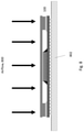
- FIG. 8 shows an example embodiment which uses airflow 800 to control the cooling of a semiconductor device.
- airflow is directed to the top of the package 100 .
- One possible way the airflow may be applied is by using the cooling nozzle 322 of FIG. 3 .
- the cooling rate of the package 100 may be increased to more closely align with the cooling rate of the circuit card 802 .
- Controlling the cooling process adds an important mechanical member to the overall structure and can significantly influence the final compressive stress in the thermal interface material. Furthermore, conditions are described in which gradients of a particular sign are deliberately created so as to increase the compression beyond its original value.
- FIG. 9 illustrates is a logic flow diagram for circuit card attachment for enhanced robustness of thermal performance, and illustrates the operation of an exemplary method, a result of execution of computer program instructions embodied on a computer readable memory, functions performed by logic implemented in hardware, and/or interconnected means for performing functions in accordance with exemplary embodiments. It assumed that a reflow oven, e.g. 300 of FIG. 3 , perform the blocks in FIG. 9 , but the blocks may also be performed by an external computer capable of controlling the reflow oven.
- a reflow oven e.g. 300 of FIG. 3
- the semiconductor device may comprise a chip connected to the packaging laminate, a thermal interface material, and a heat spreader, the thermal interface material located between a side of the chip opposite the packaging laminate and the heat spreader, and the heating and the cooling may be controlled so as to enhance a compression of the thermal interface material relative to heating and cooling without the control.
- Heating the semiconductor device may comprise heating the semiconductor device in a reflow oven having a first set of heaters above the semiconductor device and a second set of heaters below the semiconductor device, wherein at least one of the first set of heaters and the second set of heaters may be individually adjusted to apply a higher temperature on a side of the printed circuit card opposite the electronic module.
- the device heating profile may comprise a plateau heating region, a peak temperature, and a reflow region, and the higher temperature may be applied during the reflow region of the device heating profile.
- the cooling may comprise placing heat resistant coverings in contact with the printed circuit card or in close proximity to the printed circuit card to slow the rate of cooling of the printed circuit card in regions of the printed circuit card where cooling to solidification is occurring.
- the heat resistant coverings may provide insulation against a cooling effect of air surrounding the printed circuit card.
- the heat resistant coverings may provide increased thermal mass to slow the cooling of the printed circuit card.
- the cooling may comprise increasing the cooling rate of the electronic module by providing air flow onto the electronic module.
- the cooling may comprise increasing the cooling rate of the electronic module by transferring heat away from the electronic module by placing at least one object in close proximity to the electronic module.
- the method may further comprise directing air flow onto the at least one object, wherein the at least one object is a heat sink.
- the cooling the semiconductor device to solidify the solder material may comprise adjusting a conveyor belt speed of a reflow oven so that a temperature of the printed circuit card is kept at substantially a same temperature or a higher temperature than a temperature of an electronic module attached to the packaging laminate.
- An example embodiment may be provided in a reflow oven, for example the reflow oven 300 of FIG. 3 .
- the reflow over may comprise: a first set of heaters above a conveyor belt of the reflow oven and a second set of heaters below the conveyor belt; at least one processor; and at least one non-transitory memory including computer program code, the at least one memory and the computer program code may be configured to, with the at least one processor, cause the reflow oven to: configure at least one of the first set of heaters and the second set of heaters according to a device heating profile to melt a solder material located between an array of contact points on a printed circuit card of a semiconductor device and a corresponding array of contact points on a packaging laminate of the semiconductor device, wherein the solder material is located between the array of contact points and the corresponding array of contact points; and control a cooling rate of the semiconductor device so that a temperature of the printed circuit card is kept at substantially a same temperature or a higher temperature than a temperature of an electronic module attached to
- the configuring may comprise adjusting at least one heater of the first set heaters and/or the second set of heaters to apply a higher temperature on a side of the printed circuit card opposite the electronic module.
- the device heating profile may comprise a plateau heating region, a peak temperature, and a reflow region, and the higher temperature may be applied during the reflow region of the device heating profile.
- the at least one memory and the computer program code may be configured to, with the at least one processor, cause the reflow oven to: adjust a speed of the conveyor belt to control the cooling rate of the semiconductor device. Adjusting the speed of the conveyor belt may comprise reducing the speed of the conveyor belt in at least one portion of the reflow oven after the solder material is melted.
- the reflow oven may comprise at least one cooling nozzle located above the conveyor belt and following the first set of heaters.
- the at least one memory and the computer program code may be configured to, with the at least one processor, cause the reflow oven to perform at least one of: configure the at least one cooling nozzle to provide air flow onto the electronic module to control the cooling rate in regions of the printed circuit card where cooling to solidification is occurring; configure the at least one cooling nozzle to provide air flow onto at least one object placed on top of the electronic module, wherein the at least one object may be a heatsink which increases the cooling rate of the electronic module by transferring heat away from the electronic module.
- the at least one memory and the computer program code may be configured to, with the at least one processor to control the cooling rate of the semiconductor device so as to enhance the compression of a thermal interface material of the semiconductor device.
- the semiconductor device may comprise a chip connected to the packaging laminate, a thermal interface material, and a heat spreader, the thermal interface material located between a side of the chip opposite the packaging laminate and the heat spreader, and the heating and the cooling may be controlled so as to enhance a compression of the thermal interface material relative to heating and cooling without the control.
- the present invention may be a system, a method, and/or a computer program product at any possible technical detail level of integration
- the computer program product may include a computer readable storage medium (or media) having computer readable program instructions thereon for causing a processor to carry out aspects of the present invention
- the computer readable storage medium can be a tangible device that can retain and store instructions for use by an instruction execution device.
- the computer readable storage medium may be, for example, but is not limited to, an electronic storage device, a magnetic storage device, an optical storage device, an electromagnetic storage device, a semiconductor storage device, or any suitable combination of the foregoing.
- a non-exhaustive list of more specific examples of the computer readable storage medium includes the following: a portable computer diskette, a hard disk, a random access memory (RAM), a read-only memory (ROM), an erasable programmable read-only memory (EPROM or Flash memory), a static random access memory (SRAM), a portable compact disc read-only memory (CD-ROM), a digital versatile disk (DVD), a memory stick, a floppy disk, a mechanically encoded device such as punch-cards or raised structures in a groove having instructions recorded thereon, and any suitable combination of the foregoing.
- RAM random access memory
- ROM read-only memory
- EPROM or Flash memory erasable programmable read-only memory
- SRAM static random access memory
- CD-ROM compact disc read-only memory
- DVD digital versatile disk
- memory stick a floppy disk
- a mechanically encoded device such as punch-cards or raised structures in a groove having instructions recorded thereon
- a computer readable storage medium is not to be construed as being transitory signals per se, such as radio waves or other freely propagating electromagnetic waves, electromagnetic waves propagating through a waveguide or other transmission media (e.g., light pulses passing through a fiber-optic cable), or electrical signals transmitted through a wire.
- Computer readable program instructions described herein can be downloaded to respective computing/processing devices from a computer readable storage medium or to an external computer or external storage device via a network, for example, the Internet, a local area network, a wide area network and/or a wireless network.
- the network may comprise copper transmission cables, optical transmission fibers, wireless transmission, routers, firewalls, switches, gateway computers and/or edge servers.
- a network adapter card or network interface in each computing/processing device receives computer readable program instructions from the network and forwards the computer readable program instructions for storage in a computer readable storage medium within the respective computing/processing device.
- Computer readable program instructions for carrying out operations of the present invention may be assembler instructions, instruction-set-architecture (ISA) instructions, machine instructions, machine dependent instructions, microcode, firmware instructions, state-setting data, configuration data for integrated circuitry, or either source code or object code written in any combination of one or more programming languages, including an object oriented programming language such as Smalltalk, C++, or the like, and procedural programming languages, such as the “C” programming language or similar programming languages.
- the computer readable program instructions may execute entirely on the user's computer, partly on the user's computer, as a stand-alone software package, partly on the user's computer and partly on a remote computer or entirely on the remote computer or server.
- the remote computer may be connected to the user's computer through any type of network, including a local area network (LAN) or a wide area network (WAN), or the connection may be made to an external computer (for example, through the Internet using an Internet Service Provider).
- electronic circuitry including, for example, programmable logic circuitry, field-programmable gate arrays (FPGA), or programmable logic arrays (PLA) may execute the computer readable program instructions by utilizing state information of the computer readable program instructions to personalize the electronic circuitry, in order to perform aspects of the present invention.
- These computer readable program instructions may be provided to a processor of a general purpose computer, special purpose computer, or other programmable data processing apparatus to produce a machine, such that the instructions, which execute via the processor of the computer or other programmable data processing apparatus, create means for implementing the functions/acts specified in the flowchart and/or block diagram block or blocks.
- These computer readable program instructions may also be stored in a computer readable storage medium that can direct a computer, a programmable data processing apparatus, and/or other devices to function in a particular manner, such that the computer readable storage medium having instructions stored therein comprises an article of manufacture including instructions which implement aspects of the function/act specified in the flowchart and/or block diagram block or blocks.
- the computer readable program instructions may also be loaded onto a computer, other programmable data processing apparatus, or other device to cause a series of operational steps to be performed on the computer, other programmable apparatus or other device to produce a computer implemented process, such that the instructions which execute on the computer, other programmable apparatus, or other device implement the functions/acts specified in the flowchart and/or block diagram block or blocks.
- each block in the flowchart or block diagrams may represent a module, segment, or portion of instructions, which comprises one or more executable instructions for implementing the specified logical function(s).
- the functions noted in the blocks may occur out of the order noted in the Figures.
- two blocks shown in succession may, in fact, be executed substantially concurrently, or the blocks may sometimes be executed in the reverse order, depending upon the functionality involved.
- the different functions discussed herein may be performed in a different order and/or concurrently with each other. Furthermore, if desired, one or more of the above-described functions may be optional or may be combined.
Landscapes
- Engineering & Computer Science (AREA)
- Mechanical Engineering (AREA)
- Manufacturing & Machinery (AREA)
- Microelectronics & Electronic Packaging (AREA)
- Electric Connection Of Electric Components To Printed Circuits (AREA)
- Physics & Mathematics (AREA)
- Geometry (AREA)
Abstract
Description
Claims (10)
Priority Applications (1)
| Application Number | Priority Date | Filing Date | Title |
|---|---|---|---|
| US14/951,770 US11224927B2 (en) | 2015-11-25 | 2015-11-25 | Circuit card attachment for enhanced robustness of thermal performance |
Applications Claiming Priority (1)
| Application Number | Priority Date | Filing Date | Title |
|---|---|---|---|
| US14/951,770 US11224927B2 (en) | 2015-11-25 | 2015-11-25 | Circuit card attachment for enhanced robustness of thermal performance |
Publications (2)
| Publication Number | Publication Date |
|---|---|
| US20170148758A1 US20170148758A1 (en) | 2017-05-25 |
| US11224927B2 true US11224927B2 (en) | 2022-01-18 |
Family
ID=58719773
Family Applications (1)
| Application Number | Title | Priority Date | Filing Date |
|---|---|---|---|
| US14/951,770 Active 2037-10-30 US11224927B2 (en) | 2015-11-25 | 2015-11-25 | Circuit card attachment for enhanced robustness of thermal performance |
Country Status (1)
| Country | Link |
|---|---|
| US (1) | US11224927B2 (en) |
Families Citing this family (1)
| Publication number | Priority date | Publication date | Assignee | Title |
|---|---|---|---|---|
| DE102018219619A1 (en) * | 2018-11-16 | 2020-06-04 | Volkswagen Aktiengesellschaft | Method of cutting a continuous battery electrode material for manufacturing battery electrodes, and a battery electrode |
Citations (20)
| Publication number | Priority date | Publication date | Assignee | Title |
|---|---|---|---|---|
| US4565917A (en) * | 1984-01-18 | 1986-01-21 | Vitronics Corporation | Multi-zone thermal process system utilizing nonfocused infrared panel emitters |
| US4632294A (en) | 1984-12-20 | 1986-12-30 | International Business Machines Corporation | Process and apparatus for individual pin repair in a dense array of connector pins of an electronic packaging structure |
| US5039841A (en) * | 1987-09-11 | 1991-08-13 | Senju Metal Industry Co., Ltd. | Reflow furnace |
| US5128506A (en) * | 1990-10-30 | 1992-07-07 | Westinghouse Electric Corp. | Method and apparatus for selective infrared soldering using shielding fixtures |
| US5180096A (en) * | 1990-07-25 | 1993-01-19 | Nihon Den-Netsu Keiki Co., Ltd. | Method and apparatus for reflow-soldering of printed circuit boards |
| US5236117A (en) | 1992-06-22 | 1993-08-17 | Staktek Corporation | Impact solder method and apparatus |
| US5328087A (en) * | 1993-03-29 | 1994-07-12 | Microelectronics And Computer Technology Corporation | Thermally and electrically conductive adhesive material and method of bonding with same |
| US5461766A (en) * | 1994-01-26 | 1995-10-31 | Sun Microsystems, Inc. | Method for integrally packaging an integrated circuit with a heat transfer apparatus |
| US5647529A (en) * | 1995-03-10 | 1997-07-15 | Motorola, Inc. | Method of controlling the temperature of a portion of an electronic part during solder reflow |
| US20020139792A1 (en) * | 2001-02-02 | 2002-10-03 | The Furukawa Electric Co., Ltd. | Method of and apparatus for thermal analysis, method of and apparatus for calculating thermal conditions, computer product |
| US6501051B1 (en) * | 1999-08-23 | 2002-12-31 | Radient Technology Corp. | Continuous-conduction wafer bump reflow system |
| US6794616B1 (en) | 2003-04-09 | 2004-09-21 | Visteon Global Technologies, Inc. | Solder reflow oven |
| US20050161252A1 (en) | 2002-03-15 | 2005-07-28 | Dietmar Birgel | Method for fitting out and soldering a circuit board, reflow oven and circuit board for said method |
| US7156283B2 (en) | 2000-12-11 | 2007-01-02 | L'air Liquide, Societe Anonyme A Directoire Et Conseil De Surveillance Pour L'etude Et L'exploitation Des Procedes Georges Claude | Method for making a solder between metallic balls of an electronic component and mounting lands of a circuit and soldering furnace therefor |
| US20090020590A1 (en) * | 2007-07-17 | 2009-01-22 | International Business Machines Corporation | PROCESS FOR MAKING INTERCONNECT SOLDER Pb-FREE BUMPS FREE FROM ORGANO-TIN/TIN DEPOSITS ON THE WAFER SURFACE |
| US20110073637A1 (en) | 2009-09-25 | 2011-03-31 | Spx Corporation | Reflow Air Management System and Method |
| US20120052632A1 (en) * | 2010-08-25 | 2012-03-01 | Kabushiki Kaisha Toshiba | Method for manufacturing semiconductor device |
| US8501545B2 (en) | 2010-03-31 | 2013-08-06 | Globalfoundries Inc. | Reduction of mechanical stress in metal stacks of sophisticated semiconductor devices during die-substrate soldering by an enhanced cool down regime |
| US20140256090A1 (en) * | 2013-03-07 | 2014-09-11 | International Business Machines Corporation | Selective area heating for 3d chip stack |
| US20140367847A1 (en) * | 2013-06-14 | 2014-12-18 | Laird Technologies, Inc. | Methods for establishing thermal joints between heat spreaders or lids and heat sources |
-
2015
- 2015-11-25 US US14/951,770 patent/US11224927B2/en active Active
Patent Citations (21)
| Publication number | Priority date | Publication date | Assignee | Title |
|---|---|---|---|---|
| US4565917B1 (en) * | 1984-01-18 | 1999-06-08 | Vitronics Corp | Multi-zone thermal process system utilizing nonfocused infared panel emitters |
| US4565917A (en) * | 1984-01-18 | 1986-01-21 | Vitronics Corporation | Multi-zone thermal process system utilizing nonfocused infrared panel emitters |
| US4632294A (en) | 1984-12-20 | 1986-12-30 | International Business Machines Corporation | Process and apparatus for individual pin repair in a dense array of connector pins of an electronic packaging structure |
| US5039841A (en) * | 1987-09-11 | 1991-08-13 | Senju Metal Industry Co., Ltd. | Reflow furnace |
| US5180096A (en) * | 1990-07-25 | 1993-01-19 | Nihon Den-Netsu Keiki Co., Ltd. | Method and apparatus for reflow-soldering of printed circuit boards |
| US5128506A (en) * | 1990-10-30 | 1992-07-07 | Westinghouse Electric Corp. | Method and apparatus for selective infrared soldering using shielding fixtures |
| US5236117A (en) | 1992-06-22 | 1993-08-17 | Staktek Corporation | Impact solder method and apparatus |
| US5328087A (en) * | 1993-03-29 | 1994-07-12 | Microelectronics And Computer Technology Corporation | Thermally and electrically conductive adhesive material and method of bonding with same |
| US5461766A (en) * | 1994-01-26 | 1995-10-31 | Sun Microsystems, Inc. | Method for integrally packaging an integrated circuit with a heat transfer apparatus |
| US5647529A (en) * | 1995-03-10 | 1997-07-15 | Motorola, Inc. | Method of controlling the temperature of a portion of an electronic part during solder reflow |
| US6501051B1 (en) * | 1999-08-23 | 2002-12-31 | Radient Technology Corp. | Continuous-conduction wafer bump reflow system |
| US7156283B2 (en) | 2000-12-11 | 2007-01-02 | L'air Liquide, Societe Anonyme A Directoire Et Conseil De Surveillance Pour L'etude Et L'exploitation Des Procedes Georges Claude | Method for making a solder between metallic balls of an electronic component and mounting lands of a circuit and soldering furnace therefor |
| US20020139792A1 (en) * | 2001-02-02 | 2002-10-03 | The Furukawa Electric Co., Ltd. | Method of and apparatus for thermal analysis, method of and apparatus for calculating thermal conditions, computer product |
| US20050161252A1 (en) | 2002-03-15 | 2005-07-28 | Dietmar Birgel | Method for fitting out and soldering a circuit board, reflow oven and circuit board for said method |
| US6794616B1 (en) | 2003-04-09 | 2004-09-21 | Visteon Global Technologies, Inc. | Solder reflow oven |
| US20090020590A1 (en) * | 2007-07-17 | 2009-01-22 | International Business Machines Corporation | PROCESS FOR MAKING INTERCONNECT SOLDER Pb-FREE BUMPS FREE FROM ORGANO-TIN/TIN DEPOSITS ON THE WAFER SURFACE |
| US20110073637A1 (en) | 2009-09-25 | 2011-03-31 | Spx Corporation | Reflow Air Management System and Method |
| US8501545B2 (en) | 2010-03-31 | 2013-08-06 | Globalfoundries Inc. | Reduction of mechanical stress in metal stacks of sophisticated semiconductor devices during die-substrate soldering by an enhanced cool down regime |
| US20120052632A1 (en) * | 2010-08-25 | 2012-03-01 | Kabushiki Kaisha Toshiba | Method for manufacturing semiconductor device |
| US20140256090A1 (en) * | 2013-03-07 | 2014-09-11 | International Business Machines Corporation | Selective area heating for 3d chip stack |
| US20140367847A1 (en) * | 2013-06-14 | 2014-12-18 | Laird Technologies, Inc. | Methods for establishing thermal joints between heat spreaders or lids and heat sources |
Also Published As
| Publication number | Publication date |
|---|---|
| US20170148758A1 (en) | 2017-05-25 |
Similar Documents
| Publication | Publication Date | Title |
|---|---|---|
| US11029475B2 (en) | Frame lid for in-package optics | |
| US9301429B2 (en) | Thermal blocker for mobile device skin hot spot management | |
| TWI728086B (en) | Installation device and installation method | |
| US9534960B2 (en) | Method for measuring temperature using a thermistor | |
| TWI621230B (en) | Removable substrate for controlling distortion of integrated circuit package | |
| WO2009090816A1 (en) | Stage for substrate temperature control apparatus | |
| KR102270748B1 (en) | Device and method of attaching solder ball, and method of fabricating a semiconductor package including the same | |
| US11224927B2 (en) | Circuit card attachment for enhanced robustness of thermal performance | |
| Arik et al. | Effect of chip and bonding defects on the junction temperatures of high-brightness light-emitting diodes | |
| JP6151461B2 (en) | Warpage control of substrates using tempered glass with unidirectional heating | |
| KR102157253B1 (en) | Apparatus for Bonding Electronic Devices Using Laser | |
| US10249516B2 (en) | Underfill dispensing using funnels | |
| US7443685B2 (en) | Conductive heat transfer for electrical devices from the solder side and component side of a circuit card assembly | |
| CN107980014B (en) | Apparatus, method and system for non-uniform cooling of planar objects | |
| US20170176516A1 (en) | Thermal Head with a Thermal Barrier for Integrated Circuit Die Processing | |
| KR20200108340A (en) | How to cure solder paste on a heat fragile substrate | |
| JP2011514663A (en) | Method and apparatus for heat transfer of parts | |
| JP5812609B2 (en) | Heating device | |
| WO2019052237A1 (en) | Assembly method and device for circuit structural member, and circuit structural member | |
| US20190202136A1 (en) | Component coupling via plurality of adhesive elements | |
| KR102221257B1 (en) | Apparatus for heating a substrate | |
| CN224006953U (en) | Electro-optical equipment | |
| US20230326810A1 (en) | Microwave heating device and method for manufacturing semiconductor packaging using the same | |
| Ticknor et al. | Efficient passive and active wavelength-stabilization techniques for AWGs and integrated optical filters | |
| TWI724899B (en) | Capacitive element heat dissipation structure of controller |
Legal Events
| Date | Code | Title | Description |
|---|---|---|---|
| AS | Assignment |
Owner name: INTERNATIONAL BUSINESS MACHINES CORPORATION, NEW YORK Free format text: ASSIGNMENT OF ASSIGNORS INTEREST;ASSIGNORS:GAYNES, MICHAEL;YARMCHUK, EDWARD J.;REEL/FRAME:037139/0266 Effective date: 20151124 Owner name: INTERNATIONAL BUSINESS MACHINES CORPORATION, NEW Y Free format text: ASSIGNMENT OF ASSIGNORS INTEREST;ASSIGNORS:GAYNES, MICHAEL;YARMCHUK, EDWARD J.;REEL/FRAME:037139/0266 Effective date: 20151124 |
|
| STPP | Information on status: patent application and granting procedure in general |
Free format text: DOCKETED NEW CASE - READY FOR EXAMINATION |
|
| STPP | Information on status: patent application and granting procedure in general |
Free format text: NON FINAL ACTION MAILED |
|
| STPP | Information on status: patent application and granting procedure in general |
Free format text: RESPONSE TO NON-FINAL OFFICE ACTION ENTERED AND FORWARDED TO EXAMINER |
|
| STPP | Information on status: patent application and granting procedure in general |
Free format text: FINAL REJECTION MAILED |
|
| STPP | Information on status: patent application and granting procedure in general |
Free format text: ADVISORY ACTION MAILED |
|
| STPP | Information on status: patent application and granting procedure in general |
Free format text: FINAL REJECTION MAILED |
|
| STPP | Information on status: patent application and granting procedure in general |
Free format text: RESPONSE AFTER FINAL ACTION FORWARDED TO EXAMINER |
|
| STPP | Information on status: patent application and granting procedure in general |
Free format text: ADVISORY ACTION MAILED |
|
| STPP | Information on status: patent application and granting procedure in general |
Free format text: DOCKETED NEW CASE - READY FOR EXAMINATION |
|
| STPP | Information on status: patent application and granting procedure in general |
Free format text: NOTICE OF ALLOWANCE MAILED -- APPLICATION RECEIVED IN OFFICE OF PUBLICATIONS |
|
| STPP | Information on status: patent application and granting procedure in general |
Free format text: PUBLICATIONS -- ISSUE FEE PAYMENT RECEIVED |
|
| STPP | Information on status: patent application and granting procedure in general |
Free format text: PUBLICATIONS -- ISSUE FEE PAYMENT VERIFIED |
|
| STCF | Information on status: patent grant |
Free format text: PATENTED CASE |
|
| MAFP | Maintenance fee payment |
Free format text: PAYMENT OF MAINTENANCE FEE, 4TH YEAR, LARGE ENTITY (ORIGINAL EVENT CODE: M1551); ENTITY STATUS OF PATENT OWNER: LARGE ENTITY Year of fee payment: 4 |