US11218661B2 - Signal processing apparatus, photoelectric conversion apparatus, imaging apparatus, and moving body - Google Patents
Signal processing apparatus, photoelectric conversion apparatus, imaging apparatus, and moving body Download PDFInfo
- Publication number
- US11218661B2 US11218661B2 US17/124,311 US202017124311A US11218661B2 US 11218661 B2 US11218661 B2 US 11218661B2 US 202017124311 A US202017124311 A US 202017124311A US 11218661 B2 US11218661 B2 US 11218661B2
- Authority
- US
- United States
- Prior art keywords
- signal
- digital
- unit
- data
- analog
- Prior art date
- Legal status (The legal status is an assumption and is not a legal conclusion. Google has not performed a legal analysis and makes no representation as to the accuracy of the status listed.)
- Active
Links
Images


Classifications
-
- H04N5/378—
-
- H—ELECTRICITY
- H04—ELECTRIC COMMUNICATION TECHNIQUE
- H04N—PICTORIAL COMMUNICATION, e.g. TELEVISION
- H04N25/00—Circuitry of solid-state image sensors [SSIS]; Control thereof
- H04N25/70—SSIS architectures; Circuits associated therewith
- H04N25/76—Addressed sensors, e.g. MOS or CMOS sensors
- H04N25/78—Readout circuits for addressed sensors, e.g. output amplifiers or A/D converters
-
- H—ELECTRICITY
- H04—ELECTRIC COMMUNICATION TECHNIQUE
- H04N—PICTORIAL COMMUNICATION, e.g. TELEVISION
- H04N25/00—Circuitry of solid-state image sensors [SSIS]; Control thereof
- H04N25/60—Noise processing, e.g. detecting, correcting, reducing or removing noise
- H04N25/616—Noise processing, e.g. detecting, correcting, reducing or removing noise involving a correlated sampling function, e.g. correlated double sampling [CDS] or triple sampling
-
- H—ELECTRICITY
- H04—ELECTRIC COMMUNICATION TECHNIQUE
- H04N—PICTORIAL COMMUNICATION, e.g. TELEVISION
- H04N25/00—Circuitry of solid-state image sensors [SSIS]; Control thereof
- H04N25/60—Noise processing, e.g. detecting, correcting, reducing or removing noise
- H04N25/618—Noise processing, e.g. detecting, correcting, reducing or removing noise for random or high-frequency noise
-
- H04N5/357—
-
- H—ELECTRICITY
- H04—ELECTRIC COMMUNICATION TECHNIQUE
- H04N—PICTORIAL COMMUNICATION, e.g. TELEVISION
- H04N25/00—Circuitry of solid-state image sensors [SSIS]; Control thereof
- H04N25/60—Noise processing, e.g. detecting, correcting, reducing or removing noise
- H04N25/65—Noise processing, e.g. detecting, correcting, reducing or removing noise applied to reset noise, e.g. KTC noise related to CMOS structures by techniques other than CDS
Definitions
- the present disclosure relates to a signal processing apparatus, a photoelectric conversion apparatus, an imaging apparatus, and a moving body.
- Japanese Patent Application Laid-Open No. 2010-252140 discusses a complementary metal-oxide-semiconductor (CMOS) image sensor including a plurality of pixels and a plurality of AD conversion circuits.
- CMOS image sensor is a mode of a photoelectric conversion apparatus and is a mode of a signal processing apparatus performing signal processing, such as AD conversion inside.
- a plurality of AD conversion circuits is connected to a pixel column.
- the plurality of AD conversion circuits each converts a common analog signal output from a pixel into a digital signal. Such processing for performing a plurality of AD conversions on a pixel signal is sometimes referred to as multi-sampling AD conversion or simply as multi-sampling.
- the plurality of AD conversion circuits is provided with a plurality of ramp signals different from each other.
- the plurality of ramp signals is offset by certain voltages at the same time.
- some but not all of the plurality of digital signals (digital data) obtained by the AD conversions can be saturated.
- data calculation such as arithmetic average processing on the multi-sampled digital data fails to provide an accurate average result. This can sometimes result in a drop in image quality.
- AD conversion is unable to be performed because of the occurrence of noise or a surge in some of the AD conversion circuits. Consequently, the result of the data calculation on the AD-converted digital data can be inaccurate.
- a signal processing apparatus includes an analog-to-digital conversion unit, a determination unit, and a data calculation unit.
- the analog-to-digital conversion unit is configured to perform a plurality of analog-to-digital conversions on one analog signal to generate at least a plurality of digital signals including a first digital signal and a second digital signal, first noise digital data, and second noise digital data.
- the determination unit is configured to perform a determination on at least one of the plurality of digital signals.
- the determination unit includes a comparator configured to compare the digital signal subjected to the determination with a threshold.
- the data calculation unit is configured to perform calculation using the first and second digital signals.
- the data calculation unit is configured to generate a first calculation result by performing calculation including processing for averaging the first and second digital signals or processing for adding the first and second digital signals.
- the data calculation unit is configured to generate a second calculation result based on a difference between the first digital signal and the first noise digital data.
- the data calculation unit is further configured to switch whether to output the first calculation result or output the second calculation result, based on a comparison result of the comparator, is provided.
- an imaging apparatus includes a pixel unit, an analog-to-digital conversion unit; a comparator, and a data calculation unit.
- the pixel unit includes a plurality of pixels arranged in a matrix including a plurality of rows and a plurality of columns.
- the analog-to-digital conversion unit is configured to perform a plurality of analog-to-digital conversions on a signal to generate at least first digital data and second digital data and perform a plurality of analog-to-digital conversions on a noise signal to generate at least first noise digital data and second noise digital data.
- the signal is based on incident light and generated by a first pixel of the pixel unit.
- the noise signal is generated by the first pixel.
- the comparator is configured to compare at least the second digital data with a threshold.
- the data calculation unit is configured to perform calculation using the first digital data and the second digital data.
- the data calculation unit is configured to generate a first calculation result by performing calculation including processing for averaging the first digital data and the second digital data or processing for adding the first digital data and the second digital data.
- the data calculation unit is configured to generate a second calculation result based on a difference between the first digital data and the first noise digital data.
- the data calculation unit is further configured to switch whether to output first calculation result or output the second calculation result, based on a comparison result of the comparator, is provided.
- FIGS. 1A to 1C are diagrams schematically illustrating configurations of a signal processing apparatus.
- FIG. 2 is a block diagram schematically illustrating a configuration of an imaging apparatus.
- FIG. 3 is a diagram schematically illustrating a configuration of a pixel unit and peripheral circuits in the imaging apparatus.
- FIG. 4 is an equivalent circuit diagram of a pixel.
- FIG. 5 is a diagram schematically illustrating a configuration of a horizontal transfer unit.
- FIG. 6 is a block diagram schematically illustrating a configuration of a data processing unit.
- FIGS. 7A and 7B are block diagrams schematically illustrating a configuration of a data calculation unit.
- FIGS. 8A, 8B, and 8C are a timing chart for describing an operation of the imaging apparatus.
- FIG. 9 is a diagram schematically illustrating a configuration of a pixel unit and peripheral circuits in an imaging apparatus.
- FIG. 10 is a schematic diagram schematically illustrating a configuration of a horizontal transfer unit.
- FIG. 11 is a block diagram schematically illustrating a configuration of a data processing unit.
- FIG. 12 is a block diagram schematically illustrating a configuration of an N data storage unit.
- FIGS. 13A and 13B are block diagrams schematically illustrating a configuration of a data calculation unit.
- FIGS. 14A, 14B, and 14C are a timing chart for describing an operation of the imaging apparatus.
- FIGS. 15A, 15B, and 15C are a timing chart for describing an operation of the imaging apparatus.
- FIG. 16A is a diagram schematically illustrating an appearance and main internal structures of a moving body
- FIG. 16B is a block diagram schematically illustrating a configuration of the moving body.
- the circuit may also be an arithmetic or logical circuits to perform arithmetic or logical operations such as additions, subtractions, AND, OR.
- a unit may refer to a module or a functionality that is performed by a processor executing a program or instructions stored in a memory device or circuit to carry out a specified operation.
- FIGS. 1A to 1C schematically illustrate configurations of a signal processing apparatus 1 according to the present exemplary embodiment.
- the signal processing apparatus 1 illustrated in FIG. 1A includes an analog-to-digital (AD) converter or conversion unit or conversion circuit 3 and a determination unit or circuit 5 .
- AD analog-to-digital
- the AD conversion unit 3 performs a plurality of AD conversions on an analog signal (analog data) input from a node IN. As a result, the AD conversion unit 3 receiving the input of an analog signal outputs more digital signals (pieces of digital data) than the number of input signals. In the signal processing apparatus 1 illustrated in FIG. 1A , the AD conversion unit 3 receives one analog signal and sequentially outputs two or more digital signals that are the converted results of the one analog signal.
- the determination unit or circuit 5 performs determination processing on at least part of the plurality of digital signals output from the AD conversion unit 3 .
- the determination processing can be performed on only some of the plurality of digital signals.
- the determination processing is performed on either one of two digital signals and not on the other.
- the determination processing can be performed on all the plurality of digital signals.
- a digital signal typically includes a plurality of bit signals.
- the determination processing may be performed on only some of the plurality of bit signals (for example, only the most significant bit signal) included in a digital signal. Alternatively, the determination processing may be performed on only some of the bit signals in each of the plurality of digital signals.
- the signal processing apparatus 1 can perform certain determination processing on the digital signals obtained by the AD conversions. As a result, the performance of the signal processing can be improved.
- the determination unit 5 determines whether a digital signal is odd value or even value. This improves the performance of signal processing, for example, by enabling the signal processing on only odd or even digital signals. Whether a digital signal is odd value or even value can be determined by various methods. For example, the determination may be performed based on the least significant bit signal.
- the determination unit 5 determines whether a digital signal include an error or the probability of an error being included. This enables the signal processing apparatus 1 or the user of the signal processing apparatus 1 to determine reliability of the result of the signal processing. Alternatively, the signal processing apparatus 1 can change the subsequent signal processing based on the presence or absence of an error or the probability of an error. Such signal processing is thus of high performance compared to signal processing where no error-related information is output. In other words, the determination unit 5 improves the performance of the signal processing.
- An error can be determined by using various methods. For example, an error can be determined by comparing an obtained digital signal with another digital signal expected to be likely to have a close signal value.
- the AD conversion unit 3 according to the present exemplary embodiment outputs a plurality of digital signals for the same analog signal. An error can thus be accurately determined by comparing the plurality of digital signals with each other.
- the determination unit 5 performs inverse conversion on the obtained digital signals. Specifically, the determination unit 5 converts the digital signals into analog signals. The determination unit 5 then determines an error by comparing the analog signal input to the AD conversion unit 3 with the analog signals obtained by the inverse conversion.
- the determination unit 5 may include a trained model generated by machine learning or deep learning. The digital signals are input to the trained model, and the trained model outputs a signal indicating the presence or absence of an error or the probability of an error.
- the determination unit 5 calculates an error correction code for the digital signals. This enables the signal processing apparatus 1 to output the result of the signal processing along with the error correction code. In other words, the determination unit 5 improves the performance of the signal processing.
- An error correction code can be calculated by using various conventional techniques.
- the determination unit 5 compares a digital signal with a predetermined threshold.
- the signal processing apparatus 1 can change the subsequent signal processing based on the comparison result. In other words, this enables signal processing of higher performance.
- the signal processing apparatus 1 can perform processing for adding a plurality of digital signals.
- some of the digital signals are excluded from the addition processing to prevent the added result from overflowing.
- the signal value of the analog signal can be determined to have reached a saturation level, i.e. not reflect correct information.
- Such a digital signal can be excluded from the subsequent processing (such as the foregoing addition processing), or subjected to correction or replacement processing.
- the usage of the determination result of the determination unit 5 is not limited to the foregoing.
- the signal processing apparatus 1 can change the procedure of the subsequent signal processing based on the determination result. Such processing is an example of the signal processing of improved performance.
- the signal processing apparatus 1 displays the determination result to the user or notifies the user of the determination result. Since the user can obtain information about the reliability of the signal processing or other additional information, such processing is an example of the signal processing of improved performance.
- the signal processing apparatus 1 can also improve the performance of the signal processing by simply storing data indicating the determination result in an internal or external memory.
- a reliability (the frequency of errors relative to the number of times of AD conversions) related evaluation can be performed by analyzing the data indicating the determination result.
- the signal processing capable of quantitative evaluation is signal processing of improved performance. Since the determination result can thus be used in many modes of application, the performance of the signal processing can be improved by the determination unit 5 performing the determination processing.
- the analog signal input to the AD conversion unit or circuit 3 is not limited in particular.
- an analog signal generated by a sensor is input.
- the applicable sensor include a sound sensor, a vibration sensor, a temperature sensor, a pressure sensor, an optical sensor, an acceleration sensor, a brain wave sensor, and a living body sensor.
- Such sensors convert a physical quantity into an electrical signal.
- the optical sensor include a charge-coupled device (CCD) image sensor, a complementary metal-oxide-semiconductor (CMOS) image senor, a time-of-flight (ToF) sensor, and an infrared sensor.
- CCD charge-coupled device
- CMOS complementary metal-oxide-semiconductor
- ToF time-of-flight
- the AD conversion unit or circuit 3 performs AD conversions such as sloped AD conversion, successive approximation AD conversion, pipelined AD conversion, and recursive AD conversion.
- the AD conversion unit 3 typically includes a comparator. Aside from the comparator, the AD conversion unit 3 can include components to be used based on the AD conversion format.
- the signal processing apparatus 1 illustrated in FIG. 1B includes a plurality of memory units, devices, or circuits 7 connected to the AD conversion unit 3 in addition to the AD conversion unit 3 and the determination unit 5 . While FIG. 1B illustrates two memory units 7 a and 7 b , the number of memory units 7 may be three or more. Each of the plurality of memory units 7 stores at least one digital signal output from the AD conversion unit 3 . Simultaneously inputting a digital signal into the plurality of memory units 7 enables the plurality of memory units 7 to store the digital signal each. Alternatively, as described in FIG.
- the AD conversion unit 3 can perform a plurality of AD conversions on an analog signal in succession.
- the plurality of digital signals output in succession may be stored into the plurality of memory units 7 in order.
- a multiplexer and/or a switch circuit can be inserted between the AD conversion unit 3 and the memory units 7 .
- the memory units 7 and the AD conversion 3 are illustrated as separate blocks for the sake of convenience. However, the memory units 7 can be configured as part of the AD conversion unit 3 , depending on the AD conversion format.
- the determination unit 5 performs determination processing on the digital signal(s) stored in at least some of the memory units 7 . Any of the types of determination processing described in FIG. 1A can be applied to the determination unit 5 illustrated in FIG. 1B . In FIG. 1B , the determination unit 5 is connected to only the memory unit 7 a . However, the determination unit 5 may be connected to both the memory units 7 a and 7 B. Alternatively, another not-illustrated determination unit may be added and connected to the memory unit 7 b.
- the signal processing apparatus 1 illustrated in FIG. 1C includes a plurality of AD conversion units 3 connected to an input node IN. Even in such a configuration, the signal processing apparatus 1 or the AD conversion units 3 included in the signal processing apparatus 1 can perform a plurality of AD conversions on an analog signal.
- the signal processing apparatus 1 illustrated in FIG. 1C includes a determination unit 5 a connected to an AD conversion unit 3 a and a determination unit 5 b connected to an AD conversion unit 3 b .
- the AD conversion units 3 a and 3 b each have similar functions to those of the AD conversion unit 3 described in FIGS. 1A and 1B .
- the determination units 5 a and 5 b each have similar functions to those of the determination unit 5 described in FIGS. 1A and 1B .
- a signal processing circuit may be inserted into the previous stage of each of the AD conversion units 3 a and 3 b .
- amplifiers for amplifying a signal or offset addition units for adding an offset can be inserted.
- Such circuits can perform different signal processing on a signal.
- amplifiers add different gains to the analog signal input to the AD conversion unit 3 a and the analog signal input to the AD conversion unit 3 b .
- offset addition units add different amounts of offset to the analog signal input to the AD conversion unit 3 a and the analog signal input to the AD conversion unit 3 b .
- the AD conversion units 3 a and 3 b can be said to perform a plurality of AD conversions on an analog signal, since the original analog signal is the same one.
- the signal processing apparatus 1 is described to include two AD conversion units 3 .
- the same configuration may be interpreted as an AD conversion unit 3 including a plurality of AD conversion circuits or a plurality of AD converters.
- a plurality of circuits each performing AD conversion may collectively constitute one AD conversion unit 3 .
- an AD converter and an AD conversion circuit are synonymous.
- the signal processing apparatuses 1 illustrated in FIGS. 1A to 1C perform a plurality of AD conversions on an analog signal.
- the signal processing apparatuses 1 include a determination unit or units (circuit or circuits) for performing determination processing on at least part of the plurality of digital signals obtained. With such a configuration, the performance of the signal processing can be improved.
- a signal processing apparatus 1 does not necessarily need to include the AD conversion unit(s) 3 as long as a unit that obtains a plurality of digital signals converted from an analog signal is included.
- another device may generate a plurality of digital signals, and the signal processing apparatus 1 according to the present exemplary embodiment may simply receive the digital signals.
- the effect of the present exemplary embodiment does not depend on the agents that perform the foregoing respective processes, either.
- the performance of the signal processing can be improved by a method including the step of obtaining a plurality of digital signals converted from an analog signal and the step of performing determination processing on at least part of the plurality of digital signals obtained.
- FIG. 2 is a block diagram schematically illustrates a configuration of an imaging apparatus 100 according to the present exemplary embodiment.
- the imaging apparatus 100 is used as a CMOS image sensor, a ToF sensor, or an infrared sensor described in the first exemplary embodiment.
- the imaging apparatus 100 is controlled by a central processing unit (CPU) 101 .
- the imaging apparatus 100 includes a control unit or circuit 102 that operates by receiving a synchronization signal and communication from the CPU 101 .
- the imaging apparatus 100 includes a vertical scanning unit or circuit 103 that operates by receiving control signals from the control unit 102 , and a pixel unit or circuit 104 where a plurality of pixels P is arranged in an n-row m-column matrix.
- the vertical scanning unit 103 controls operation of the pixel unit 104 .
- the imaging apparatus 100 further includes a column AD conversion unit or circuit 105 that processes signals from the pixel unit 104 , and a horizontal transfer unit or circuit 106 , a data processing unit or circuit 107 , and a signal output unit or circuit 108 .
- the column AD conversion unit 105 and the horizontal transfer unit 106 operate by receiving control signals from the control unit 102 .
- FIG. 3 is schematic diagram illustrating a configuration example of the pixel unit 104 and the column AD conversion unit 105 according to the present exemplary embodiment.
- the pixel unit 104 includes pixels 201 in each column.
- the pixel unit 104 also includes vertical signal lines 202 connected to the pixels 201 in the respective columns.
- the vertical signal lines 202 are connected to constant current sources (not illustrated).
- the vertical signal lines 202 are also connected to offset addition units 203 .
- the outputs of the offset addition units 203 are connected to column AD converters 204 .
- the outputs of the column AD converters 204 are connected to holding units 205 .
- the column AD conversion unit 105 includes a plurality of column AD converters 204 .
- Each column AD converter 204 has similar functions to those of the AD conversion unit 3 described in the first exemplary embodiment. The description of the AD conversion unit 3 according to the first exemplary embodiment is thus incorporated in its entirety in the present exemplary embodiment.
- each column is provided with a vertical signal line 202 .
- each column is provided with an offset addition unit 203 .
- Each column is provided with two column AD converters 204 and two holding units 205 .
- the vertical signal line 202 connected to the pixels 201 in the first column is denoted by the symbol c1
- the vertical signal line 202 connected to the pixels 201 in an mth column by the symbol cm For example, an analog signal (pixel signal) from a pixel 201 connected to the vertical signal line c1 is input to the offset addition unit or circuit 203 connected to the vertical signal line c1.
- the offset addition unit 203 outputs a plurality of signals c1_ofst_# (#: 1 to 2). Signals offset by an offset addition unit 203 will also be referred to as offset signals.
- the offset addition unit 203 can include amplification circuits, such as a column amplifier, or attenuator circuits. Alternatively, a configuration capable of adding or subtracting signal values of analog signals can be used.
- the signals (output signals) c1_ofst_# of the offset addition unit 203 are input to the respective column AD converters 204 .
- the column AD converters 204 are blocks for converting analog data into digital data.
- the column AD converters 204 according to the present exemplary embodiment include a comparator, a ramp wave generator, and a counter each.
- the ramp wave generator and the counter may be shared by a plurality of column AD converters 204 .
- the outputs of the column AD converters 204 are connected to the inputs of the holding units or circuits 205 .
- the holding units 205 have similar functions to those of the memory unit(s) 7 according to the first exemplary embodiment.
- the holding units 205 may be omitted.
- the holding units 205 output signals adout_c1_# (#: 1 to 2).
- the signals adout_c1_# are digital signals (digital data) and include a plurality of bit signals each.
- FIG. 4 is a diagram illustrating an equivalent circuit of a pixel 201 according to the present exemplary embodiment.
- the pixel 201 includes a photoelectric conversion element (photodiode (PD)) 311 , a charge transfer unit or circuit 312 , a floating diffusion portion FD, a resetting unit or circuit 313 , a signal amplification unit or circuit 314 , and a row selection unit or circuit 315 .
- the photoelectric conversion element (PD) 311 includes an element, such as a PD, for generating a charge based on the amount of light incident on the photoelectric conversion element 311 .
- the charge transfer unit 312 is connected between the photoelectric conversion element (PD) 311 and the floating diffusion portion FD.
- the charge transfer unit 312 is a transfer transistor for reading the charge accumulated in the photoelectric conversion element (PD) 311 . Conduction and non-conduction (on and off) of the charge transfer unit 312 are controlled by a pixel transfer signal PTX(1).
- the resetting unit 313 is connected between a power supply voltage VDD and the floating diffusion portion FD.
- the resetting unit 313 is a resetting transistor for supplying the power supply voltage VDD to the floating diffusion portion FD to reset the circuit. Conduction and non-conduction (on and off) of the resetting unit 313 are controlled by a pixel unit reset signal PRES(1).
- the floating diffusion portion FD is connected to the gate terminal of the signal amplification unit 314 .
- the power supply voltage VDD and the row selection unit 315 are connected to the drain and source terminals.
- the signal amplification unit 314 is a source-follower transistor for converting the charge accumulated in the floating diffusion portion FD into a voltage, amplifying the voltage, and outputting the amplified voltage as a voltage signal to the vertical signal line 202 .
- the row selection unit 315 is connected between the output of the signal amplification unit 314 and the vertical signal line 202 .
- the row selection unit 315 is a transistor for selecting the row to output a pixel signal. Conduction and non-conduction (on and off) of the row selection unit 315 are controlled by a row selection signal PSEL(1).
- FIG. 5 is a diagram illustrating a configuration example of the horizontal transfer unit 106 according to the present exemplary embodiment.
- the horizontal transfer unit 106 includes a plurality of three-state buffers 401 , horizontal transfer lines 402 , and a horizontal scanning unit 403 .
- the signals adout_cM_# (M: 1 to m) (#: 1 to 2) output from the column AD conversion unit 105 are connected to the inputs of the respective three-state buffers 401 .
- the outputs of the three-state buffers 401 are connected to the horizontal transfer lines 402 .
- the outputs of the three-state buffers 401 are controlled by the horizontal scanning unit 403 .
- the three-state buffers 401 can select to “simply output their input signal” or to “output no signal (high impedance state)”.
- each column is provided with two channels (ch) of horizontal transfer lines 402 .
- the signal adout_cM_1 is connected to a horizontal transfer line 402 ch_1 via a three-state buffer 401
- the signal adout_cM_2 is connected to a horizontal transfer line 402 ch_2 via another three-state buffer 401 .
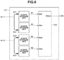
- FIG. 6 is a diagram illustrating a configuration example of the data processing unit 107 according to the present exemplary embodiment.
- the data processing unit 107 includes S data storage units or circuits 501 and 503 , N data storage units or circuits 502 and 504 , and a data calculation unit or circuit 505 .
- N data and S data are two signals obtained to perform correlated double sampling (CDS) in the imaging apparatus 100 .
- CDS correlated double sampling
- Two pieces of analog data output from a pixel 201 are individually AD-converted into N data and S data.
- S data refers to digital data obtained by performing AD conversion on a signal (light signal) based on incident light to be described below.
- N data refers to noise digital data obtained by performing AD conversion on a noise signal to be described below.
- the input (horizontal transfer line) ch_1 to the data processing unit 107 is connected to both the S data storage unit 501 and the N data storage unit 502 .
- the S data storage unit 501 includes an output port S1.
- the output port S1 is connected to the data calculation unit 505 .
- the N data storage unit 502 includes an output port N1.
- the output port N1 is connected to the data calculation unit 505 .
- the input (horizontal transfer line) ch_2 to the data processing unit 107 is connected to both the S data storage unit 503 and the N data storage unit 504 .
- the S data storage unit 503 includes an output port S2.
- the output port S2 is connected to the data calculation unit 505 .
- the N data storage unit 504 includes an output port N2.
- the output port N2 is connected to the data calculation unit 505 .
- the data calculation unit 505 performs calculation based on input data Sin1, Nin1, Sin2, and Nin2.
- the data calculation unit 505 outputs the calculation result to a port SN.
- the S data storage units 501 and 503 and the N data storage units 502 and 504 can include a static random access memory (SRAM) each.
- the data storage units 501 to 504 can include flip-flops.
- the data storage units 501 to 504 may be other storage elements.
- the data calculation unit 505 includes a detection unit or circuit 611 (see FIG. 7A ) that detects an anomaly or error in the data values of the AD-converted input data Sin1, Sin2, Nin1, and Nin2.
- the detection unit 611 determines the presence or absence of an error or the probability of occurrence of an error from the data values of the input data Sin1, Sin2, Nin1, and Nin2.
- the detection unit 611 is an example of the determination unit 5 according to the first exemplary embodiment.
- the data calculation unit 505 includes a unit (selector 608 to be described below) that, in a case where an error is detected by the detection unit 611 , disables use of the data including the error.
- the data calculation unit 505 thus provides an appropriate data calculation result even in a case where the AD-converted data includes an abnormal value due to reasons such as a surge, for example.
- FIG. 7A illustrates a circuit configuration of the data calculation unit 505 .
- the data calculation unit 505 includes the detection unit or circuit 611 and a data calculator or calculating circuit 610 .
- the detection unit 611 detects an anomaly or error from the data values of the input data Sin1, Sin2, Nin1, and Nin2.
- the data calculator 610 performs various data calculations on the input data Sin1, Sin2, Nin1, and Nin2.
- the data calculation unit 505 further includes a selector 608 that switches between two output results of the data calculator 610 based on the determination result of the detection unit 611 .
- FIG. 7B illustrates an example of processing of the data calculator 610 and the detection unit 611 .
- the data calculator 610 averages the S data and the N data.
- the detection unit 611 performs a determination by comparing the input data Sin2 and Nin2 with thresholds.
- the data calculation unit 505 initially obtains a difference between the input data Sin1 and the input data Nin1, or Sin1 ⁇ Nin1. In a case where the input data Sin2 is greater than a threshold thresh_S or the input data Nin2 is greater than a threshold thresh_N, the data calculation unit 505 outputs the difference between the input data Sin1 and the input data Nin1.
- the data calculation unit 505 also obtains a difference between the input data Sin2 and the input data Nin2, or Sin2 ⁇ Nin2.
- the data calculation unit 505 outputs an average of the differences Sin1 ⁇ Nin1 and Sin2 ⁇ Nin2.
- the data calculation unit 505 includes subtractors 601 and 602 , comparators 603 and 604 , an adder 605 , an average processing circuit 606 , an OR circuit 607 , and the selector 608 .
- the subtractor 601 inputs the input data Sin1 and Nin1, and outputs the result of subtraction of the input data Nin1 from the input data Sin1.
- the subtractor 602 inputs the input data Sin2 and Nin2, and outputs the result of subtraction of the input data Nin2 from the input data Sin2.
- the adder 605 adds the outputs of the subtractors 601 and 602 , and outputs the result.
- the average processing circuit 606 outputs the result of division of the output of the adder 605 by 2 .
- the average processing circuit 606 is a circuit for determining an average based on the number of pieces of input data.
- the average processing circuit 606 may be constituted by a divider as described above, or may be constituted by a shifter circuit in a case where the number of pieces of input data is a power of 2. Alternatively, the average processing circuit 606 may be omitted and the result determined by the adder 605 may be output.
- the comparator 603 compares the input data Sin2 with the threshold thresh_S. The comparator 603 outputs a high level in a case where the input data Sin2 is greater than the threshold thresh_S, and outputs a low level in the other cases.
- the comparator 604 compares the input data Nin2 with the threshold thresh_N.
- the comparator 604 outputs a high level in a case where the input data Nin2 is greater than the threshold thresh_N, and outputs a low level in the other cases.
- the OR circuit 607 inputs the outputs of the comparators 603 and 604 , and outputs the logical OR of the outputs.
- the selector 608 selects either the output of the subtractor 601 or the output of the average processing circuit 606 based on the output level of the OR circuit 607 , and outputs the selected output as SNout.
- the detection unit 611 including the comparator 603 serves as a determination unit.
- the selector 608 switches the data to be output based on the output of the detection unit 611 . In such a manner, the method of signal processing is changed based on the result output from the determination unit.
- the selector 608 may be omitted and the presence or absence of an error may be separately output to outside.
- FIGS. 8A, 8B, and 8C are a timing chart illustrating an example of operation of the column AD conversion unit 105 , the horizontal transfer unit 106 , and the data processing unit 107 .
- the imaging apparatus 100 according to the present exemplary embodiment performs AD conversion row by row, and sequentially outputs data pixel by pixel. Such operations will be described.
- As an overall procedure (1) an operation for obtaining digital data and storing the digital data in a memory (S and N data storage units 503 and 504 ), (2) an operation for reading the digital data from the memory, and (3) a calculation operation on the data read from the memory will be described in order.
- the CPU 101 outputs a horizontal synchronization signal HD to the control unit 102 .
- the control unit 102 controls the vertical scanning unit 103 .
- the pixel unit 104 outputs N (noise) signals to vertical signal lines cM (M: 1 to m) in all the columns at the same time.
- the N signals are signals obtained by cancelling the resetting of the floating diffusion portions FD and then reading the charges in the floating diffusion portions FD via the signal amplification units 314 .
- the offset addition units 203 add offsets to the signals of the vertical signal lines cM (M: 1 to m).
- Each offset addition unit 203 outputs signals cM_ofst_1 and cM_ofst_2 to which offsets of respective different values are added. As illustrated in FIG. 8A , the values of the offsets to be added are such that cM_ofst_1 ⁇ cM_ofst_2.
- the imaging apparatus 100 By the addition of the offsets, an N signal is turned into two signals having different offset values. However, the added offsets are eventually removed.
- the imaging apparatus 100 according to the present exemplary embodiment thus performs a plurality of AD conversions on an analog signal (pixel signal).
- the imaging apparatus 100 according to the present exemplary embodiment includes a configuration such that processing circuits for performing respective different processes are inserted between the input node IN and the respective AD conversion units 3 a and 3 b in FIG. 1C of the first exemplary embodiment.
- the column AD converters 204 AD-convert the outputs (signals) cM_ofst_# (M: 1 to m) (#: 1 to 2) of the offset addition units 203 in all the columns at the same time.
- N-AD an AD conversion period for the signals obtained by adding the offsets to the N signals.
- the column AD converters 204 start to generate ramp waves and operate their counters.
- the signals cM_ofst_1 intersect the voltages of the ramp waves, and counter values N1_M_t1 (M: 1 to m) at that point in time are output from the column AD converters 204 as digital data.
- the signals cM_ofst_2 intersect the voltages of the ramp waves, and counter values N2_M_t1 (M: 1 to m) at the point in time are output from the column AD converters 204 as digital data.
- the offset-added data (offset signals) have the relationship of cM_ofst_1 ⁇ cM_ofst_2.
- the results of AD conversion (counter values) N1_M_t1 of the signals cM_ofst_1 and the results of AD conversion (counter values) N2_M_t1 of the signals cM_ofst_2 during the AD conversion period N-AD thus satisfy the relationship of N1_M_t1 ⁇ N2_M_t1.
- the data transferred here includes a data group N_ch1(h1) obtained by the AD conversion of the signals cM_ofst_1 and a data group N_ch2(h1) obtained by the AD conversion of the signals cM_ofst_2.
- the data groups N_ch #(h1) (#: 1 to 2) in the holding units 205 are transferred to the data processing unit 107 via the horizontal transfer unit 106 pixel by pixel.
- the data group N_ch1(h1) is sequentially written to the N data storage unit 502 .
- the data group N_ch2(h1) is sequentially written to the N data storage unit 504 .
- FIG. 8A illustrates that the data groups N_ch #(h1) (#: 1 to 2) are written to the N data storage units 502 and 504 during the period from time T1w1 to time T1w2.
- the pixels 201 output S signals (light signals) to the vertical signal lines 202 cM (M: 1 to 2) in all the columns at the same time.
- the S signals are signals obtained by transferring the charges in the photoelectric conversion elements (PD) 311 to the floating diffusion portions FD by the charge transfer units 312 and reading the charges in the floating diffusion portions FD at that time via the signal amplification units 314 .
- the S signals are signals based on the incident light.
- the offset addition units 203 add offsets to the signals of the vertical signal lines 202 cM (M: 1 to m) in the respective columns at the same time. As illustrated in FIG. 8A , the values of the offsets to be added are such that cM_ofst_1 ⁇ cM_ofst_2.
- the column AD converters 204 AD-convert the outputs cM_ofst_# (M: 1 to m) (#: 1 to 2) of the offset addition units 203 in all the columns at the same time.
- the AD conversion period for the signals obtained by adding offsets to the S signals is denoted as S-AD.
- the column AD converters 204 start to generate ramp waves and operate their counters.
- the signals cM_ofst_1 intersect the voltages of the ramp waves, and counter values S1_M_t1 (M: 1 to m) at that point in time are output from the column AD converters 204 as digital data.
- the signals cM_ofst_2 intersect the voltages of the ramp waves, and counter values S2_M_t1 (M: 1 to m) at that point in time are output from the column AD converters 204 as digital data.
- the offset-added data (offset signals) satisfy the relationship of cM_ofst_1 ⁇ cM_ofst_2.
- the results of AD conversion (counter values) S1_M_t1 of the signals cM_ofst_1 and the results of AD conversion (counter values) S2_M_t1 of the signals cM_ofst_2 during the AD conversion period S-AD thus satisfy the relationship of S1_M_t1 ⁇ S2_M_t1.
- the data transferred here includes a data group S_ch1(h1) obtained by the AD conversion of the signals cM_ofst_1 and a data group S_ch2(h1) obtained by the AD conversion of the signals cM_ofst_2.
- the data groups S_ch #(h1) (#: 1 to 2) in the holding units 205 are transferred to the data processing unit 107 via the horizontal transfer unit 106 pixel by pixel.
- the data group S_ch1(h1) is sequentially written to the S data storage unit 501 .
- the data group S_ch2(h1) is sequentially written to the S data storage unit 503 .
- FIG. 8A illustrates that the data groups S_ch #(h1) (#: 1 to 2) are written to the S data storage units 501 and 503 during the period from time T1w3 to time T1w4.
- the CPU 101 outputs the horizontal synchronization signal HD to the control unit 102 .
- the data group N_ch1(h1) is read from the N data storage unit 502 pixel by pixel.
- the data group N_ch2(h1) is read from the N data storage unit 504 pixel by pixel.
- the data group S_ch1(h1) is also synchronously read from the S data storage unit 501 pixel by pixel.
- the data group S_ch2(h1) is read from the S data storage unit 503 pixel by pixel.
- the data in the data groups S_ch #(h1) and N_ch #(h1) (#: 1 to 2) is processed by the data calculation unit 505 pixel by pixel, and output from the signal output unit 108 .
- the operation on the first row has been described above.
- the second and subsequent rows are successively processed in a similar manner to the first row.
- the column AD converters 204 in the Mth column output signals N1_M_t1, N2_M_t1, S1_M_t1, and S2_M_t1.
- the column AD converters 204 in the Lth column output signals N1_L_t1, N2_L_t1, S1_L_t1, and S2_L_t1 (L: 1 to m, L ⁇ M).
- the data values of the N data and S data in the Mth column satisfy the relationships of N1_M_t2 ⁇ N2_M_t2 and S1_M_t2 ⁇ S2_M_t2.
- the inputs (thresholds) thresh_S and thresh_N of the data calculation unit 505 satisfy the relationships of N2_M_t2 ⁇ thresh_N and S2_M_t2 ⁇ thresh_S.
- the AD-converted data in the Mth column therefore satisfies the relationships of N2_M_t2 ⁇ thresh_N and S2_M_t2 ⁇ thresh_S in magnitude. From Eq.
- the data values of the N data and S data in the Lth column satisfy the relationships of N1_L_t2 ⁇ N2_L_t2 and S1_L_t2 ⁇ S2_L_t2.
- the input (threshold) thresh_S of the data calculation unit 505 satisfies the relationship of thresh_S ⁇ S2_L_t2. That is, the AD-converted data in the Lth column therefore satisfies the relationship of N2_L_t2>thresh_N or S2_L_t2>thresh_S in magnitude.
- the calculation result of the data calculation unit 505 is thus expressed as the following Eq. 4.
- SN out S 1_ L _ t 2 ⁇ N 1_ L _ t 2 (Eq. 4)
- two column AD converters 204 are connected to the same vertical signal line 202 .
- the detection unit 611 determines the presence or absence of an error in the plurality of pieces of digital data multi-sampled by the two column AD converters 204 .
- an imaging apparatus capable of appropriate signal processing can be provided.
- digital data containing an error is not used for image formation. As a result, the image quality of the imaging apparatus 100 can be improved.
- the detection unit 611 performs a determination on only some of the digital signals (N #_M_t1 and S #_M_t1) as determination targets.
- the detection unit 611 performs no determination on the other digital signals.
- Such a configuration can provide the effect of reducing circuit scale or reducing power consumption.
- selecting the determination targets based on the operation of the offset addition units 203 can provide an additional effect.
- the detection unit 611 performs the determination on signals to which offsets of relatively large values are added (S2_M_t1>S1_M_t1).
- the purpose of the determination is to detect saturation, and the signal values of the signals to which offsets of large values are added reach a saturation level first. Such a configuration can thus improve the image quality with a small circuit scale or low power consumption. It will be understood that the digital signals to be subjected to the determination change depending on the purpose of the determination. Alternatively, the determination may be performed on all the digital signals.
- the determination is described to be performed by comparing the digital signals with the thresholds.
- all the types of determination processing described in the first exemplary embodiment can be applied to the imaging apparatus 100 according to the present exemplary embodiment.
- the description of the first exemplary embodiment is incorporated.
- the imaging apparatus according to the present exemplary embodiment is a mode of a signal processing apparatus.
- the first exemplary embodiment has dealt with an example where a vertical signal line 202 is provided for each column and the data processing is performed row by row.
- a plurality of vertical signal lines 202 is provided for each column of pixels.
- six vertical signal lines 202 are provided for each column.
- the imaging apparatus according to the present exemplary embodiment has a first mode where AD conversion is simultaneously performed on analog signals (pixel signals) from pixels arranged in six rows, and digital data is sequentially output in units of two pixels in two rows.
- the imaging apparatus according to the present exemplary embodiment also has a second mode where AD conversion is simultaneously performed on pixel signals from pixels arranged in two rows, and the digital data on the two pixels are sequentially output.
- two AD converts are connected to a pixel to perform a plurality of AD conversions (multi-sampling).
- four AD converters are used to perform AD conversions in parallel on two pixels in one column and two rows. Since the imaging apparatus according to the present exemplary embodiment has the first mode as well, six AD converters are provided for each column. Unlike the first exemplary embodiment, each vertical signal line 202 is not provided with two column AD converters for the sake of multi-sampling in the second mode of simultaneously performing AD conversions on two rows.
- the column AD converters intended for the first mode of simultaneously performing AD conversions on six rows appropriate data processing calculations can be performed on multi-sampling data without an additional circuit.
- the imaging apparatus has a circuit configuration different from that of the first exemplary embodiment in that a plurality of vertical signal lines 202 corresponding to a column is connected to offset addition units 203 and column AD converters 204 via a selection unit 901 .
- a data calculation unit 1003 includes a mechanism (selector 1209 ) for selecting which signal to output from among those of the plurality of calculation results of the data calculator 610 based on a read mode.
- FIG. 2 is a block diagram schematically illustrating the configuration of the imaging apparatus 100 according to the present exemplary embodiment.
- FIG. 4 is a diagram illustrating an equivalent circuit of a pixel 201 according to the present exemplary embodiment.
- FIG. 9 is a schematic diagram illustrating a configuration example of a pixel unit 104 and a column AD conversion unit 105 according to the present exemplary embodiment.
- the pixel unit 104 includes pixels 201 in each column.
- the pixel unit 104 also includes vertical signal lines 202 connected to the pixels 201 in each column.
- the vertical signal lines 202 are connected to constant current sources (not illustrated).
- the vertical signal lines 202 are connected to offset addition units 203 .
- the outputs of the offset addition units 203 are connected to column AD converters 204 .
- the outputs of the column AD converters 204 are connected to holding units 205 .
- the column AD conversion unit 105 includes a plurality of column AD converters 204 .
- Each column AD converter 204 has a similar function to that of the AD conversion unit 3 described in the first exemplary embodiment. In other words, the description of the AD conversion unit 3 according to the first exemplary embodiment is incorporated in its entirety in the present exemplary embodiment.
- six vertical signal lines 202 are provided for each column.
- six offset addition units 203 are provided for each column.
- six column AD converters 204 are provided for each column.
- six holding unit 205 are provided for each column.
- c1_VL # (#: 1 to 6)
- cm_VL # six vertical signal lines 202 connected to the pixels 201 in an mth column
- the pixel 201 in the first column and the first row is connected to the vertical signal line c1_VL1.
- the pixel 201 in the first column and the second row is connected to the vertical signal line c1_VL2.
- the pixels 201 in the first column are cyclically connected to the corresponding vertical signal lines c1_VL #(#: 1 to 6) in units of six rows.
- a plurality of vertical signal lines 202 corresponding to a column are connected to offset addition units 203 and column AD converters 204 via a selection unit 901 .
- the selection unit 901 transmits the signal of a given vertical signal line 202 to one or a plurality of offset addition units 203 .
- the pixel signals output to the vertical signal lines c1_VL # are input to the selection unit 901 .
- the selection unit 901 switches which output signals c1_VL #_sel of the selection unit 901 to connect the six connected vertical lines c1_VL # (#: 1 to 6) to, and output the output signals c1_VL #_sel.
- the selection unit 901 includes multiplexers and/or switch circuits.
- the output signals c1_VL #_sel of the selection unit 901 are input to the offset addition units 203 .
- the offset addition units 203 output offset-added signals c1_VL #_ofst.
- the offset addition units 203 may include amplification circuits, such as a column amplifier, or attenuator circuits, for example. Alternatively, a configuration capable of adding or subtracting signal values of analog signals can be used.
- the output signals c1_VL #_ofst of the offset addition units 203 are input to the column AD converters 204 .
- the column AD converters 204 are blocks for converting analog data into digital data.
- the column AD converters 204 according to the present exemplary embodiment include a comparator, a ramp wave generator, and a counter each.
- the ramp wave generator and the counter may be shared by a plurality of column AD converters 204 .
- the outputs of the column AD converters 204 are connected to the inputs of the holding units 205 .
- the holding units 205 have a similar function to that of the memory unit 7 according to the first exemplary embodiment.
- the holding units 205 may be omitted.
- the holding units 205 output signals adout_c1_# (#: 1 to 6).
- the signals adout_c1_# are digital signals (digital data) and include a plurality of bit signals each.
- FIG. 10 is a diagram illustrating a configuration example of a horizontal transfer unit 106 according to the present exemplary embodiment.
- the horizontal transfer unit 106 includes a plurality of three-state buffers 401 , horizontal transfer lines 402 , and a horizontal scanning unit 403 .
- six channels of horizontal transfer lines 402 are provided for each column.
- the outputs adout_cM_VL1 of the column AD conversion unit 105 are output to a horizontal transfer line ch_VL1 via the corresponding three-state butters 401 .
- the outputs adout_cM_VL2 of the column AD conversion unit 105 are output to a horizontal transfer line ch_VL2 via the corresponding three-state buffers 401 .
- FIG. 11 is a diagram illustrating a configuration example of a data processing unit or circuit 107 according to the present exemplary embodiment.
- the data processing unit 107 includes an S data storage unit or circuit 1001 , an N data storage unit or circuit 1002 , and data calculation units or circuits 1003 and 1004 .
- N data and S data are two signals obtained to perform CDS in the imaging apparatus 100 .
- Two pieces of analog data output from a pixel 201 are AD-converted into N data and S data.
- the inputs ch_VL # (#: 1 to 6) to the data processing unit 107 are connected to both the S and N data storage units 1001 and 1002 .
- the S data storage unit 1001 includes output ports S 135 _ 1 , S 135 _ 2 , S 246 _ 1 , and S 246 _ 2 . Both the output ports S 135 _ 1 and S 135 _ 2 are connected to the data calculation unit 1003 . Both the output ports S 246 _ 1 and S 246 _ 2 are connected to the data calculation unit 1004 .
- the N data storage unit 1002 includes output ports N 135 _ 1 , N 135 _ 2 , N 246 _ 1 , and N 246 _ 2 . Both the output ports N 135 _ 1 and N 135 _ 2 are connected to the data calculation unit 1003 . Both the output ports N 246 _ 1 and N 246 _ 2 are connected to the data calculation unit 1004 .
- the data calculation unit 1003 performs calculation based on its inputs S 135 _ 1 , S 135 _ 2 , N 135 _ 1 , and N 135 _ 2 .
- the data calculation unit 1003 outputs the calculation result as an output SN 135 .
- the data calculation unit 1004 performs calculation based on its inputs S 246 _ 1 , S 246 _ 2 , N 246 _ 1 , and N 246 _ 2 .
- the data calculation unit 1004 outputs the calculation result as an output SN 246 .
- the S and N data storage units 1001 and 1002 can include an SRAM each. Within the acceptable circuit scale, the S and N data storage units 1001 and 1002 may include flip-flops. The S and N data storage units 1001 and 1002 may be other storage elements.
- the outputs S 135 _ 1 and S 135 _ 2 of the S data storage unit 1001 and the outputs N 135 _ 1 and N 135 _ 2 of the N data storage unit 1002 are each generated by selecting any one of the data on the horizontal transfer line ch_VL1, the data on the horizontal transfer line ch_VL3, and the data on the horizontal transfer line ch_VL5 stored in storage units.
- the outputs S 246 _ 1 and S 246 _ 2 of the S data storage unit 1001 and the outputs N 246 _ 1 and N 246 _ 2 of the N data storage unit 1002 are each generated by selecting any one of the data on the horizontal transfer line ch_VL2, the data on the horizontal transfer line ch_VL4, and the data on the horizontal transfer line ch_VL6 stored in storage units.
- FIG. 12 is a diagram schematically illustrating a configuration of the N data storage unit 1002 illustrated in FIG. 11 .
- the S data storage unit 1001 has a similar configuration to that of the N data storage unit 1002 .
- the N data storage unit 1002 includes a storage unit A 1101 , a storage unit B 1102 , a storage unit C 1103 , a storage unit D 1104 , a storage unit E 1105 , a storage unit F 1106 , and selectors 1107 to 1110 .
- the storage unit A 1101 to the storage unit F 1106 may include an SRAM each.
- the storage unit A 1101 to the storage unit F 1106 may include flip-flops.
- the input ch_VL1 to the N data storage unit 1002 is connected to the storage unit A 1101 .
- the input ch_VL2 is connected to the storage unit B 1102 .
- the input ch_VL3 is connected to the storage unit C 1103 .
- the input ch_VL4 is connected to the storage unit D 1104 .
- the input ch_VL5 is connected to the storage unit E 1105 .
- the input ch_VL6 is connected to the storage unit F 1106 .
- the inputs ch_VL1 to ch_VL6 to the N data storage unit 1002 are connected to the storage unit A 1101 to the storage unit F 1106 , respectively, and therefore the respective pieces of data are stored.
- the selector 1107 selects data from among an output N1 of the storage unit A 1101 , an output N3 of the storage unit C 1103 , and an output N5 of the storage unit E 1105 , and outputs the selected data to the output port N 135 _ 1 .
- the selector 1108 selects data from among the output N1 of the storage unit A 1101 , the output N3 of the storage unit C 1103 , and the output N5 of the storage unit E 1105 , and outputs the selected data to the output port N 135 _ 2 .
- the selector 1109 selects data from among an output N2 of the storage unit B 1102 , an output N4 of the storage unit D 1104 , and an output N6 of the storage unit F 1106 , and outputs the selected data to the output port N 246 _ 1 .
- the selector 1110 selects data from among the output N2 of the storage unit B 1102 , the output N4 of the storage unit D 1104 , and the output N6 of the storage unit F 1106 , and outputs the selected data to the output port N 246 _ 2 .
- the data calculation units 1003 and 1004 each include a detection unit 611 that detects an anomaly or error in the data values of AD-converted input data Sin1, Sin2, Nin1, and Nin2.
- the detection unit 611 determines the presence or absence of an error or the probability of occurrence of an error from the values of the input data.
- the detection unit 611 is an example of the detection unit 5 according to the first exemplary embodiment.
- the data calculation units 1003 and 1004 each include a unit (selector 1208 to be described below) that, in a case where an error is detected by the detection unit 611 , disables use of the data including the error.
- the data calculation units 1003 and 1004 therefore provide appropriate data calculation results even in a case where the AD-converted data includes an abnormal value due to reasons such as a surge, for example.
- FIG. 13A illustrates a circuit configuration of the data calculation unit 1003 . Since the data calculation unit 1004 has a similar configuration to that of the data calculation unit 1003 , a redundant description of the data calculation unit 1004 will hereinafter be omitted.
- the data calculation unit 1003 includes the detection unit 611 that detects an anomaly or error from the data values of the input data Sin1, Sin2, Nin1, and Nin2, and a data calculator 610 that performs various data calculations on the input data Sin1, Sin2, Nin1, and Nin2.
- the data calculation unit 1003 further includes a selector 1208 that switches between two output results of the data calculator 610 based the determination result of the detection unit 611 .
- FIG. 13B illustrates an example of processing of the data calculator 610 and the detection unit 611 .
- the data calculator 610 averages the S data and the N data.
- the detection unit 611 performs a determination by comparing the input data Sin2 and Nin2 with thresholds.
- the data calculation unit 1003 initially obtains a difference between the input data Sin1 and the input data Nin, or Sin1 ⁇ Nin1.
- the data calculation unit 1003 simply outputs the difference between the input data Sin 1 and the input data Nin1 in any of the following cases 1 to 3:
- Case 1 is where the input data Sin2 is greater than a threshold thresh_S.
- Case 2 is where the input data Nin2 is greater than a threshold thresh_N.
- Case 3 is where a signal mult_smpl_en indicates a state where multi-sampling is not performed. In the present exemplary embodiment, multi-sampling is not performed in a case where the signal mult_smpl_en is “0”.
- the output SNout is expressed by the following Eq. 5.
- SN out S in1 ⁇ N in1 (Eq. 5)
- the data calculation unit 1003 also obtains a difference between the input data Sin2 and the input data Nin2, or Sin2 ⁇ Nin2.
- the data calculation unit 1003 outputs an average of (Sin1 ⁇ Nin1) and (Sin2 ⁇ Nin2) in a case where all of the following conditions 1 to 3 are satisfied.
- Condition 1 is that the input data Sin2 is less than or equal to the threshold thresh_S.
- Condition 2 is that the input data Nin2 is less than or equal to the threshold thresh_N.
- a difference from the second exemplary embodiment is the addition of a selector 1209 for switching the value of the output SNout depending on the signal mult_smpl_en.
- the selector 1209 inputs the output of a subtractor 1201 and the output of the selector 1208 , and switches the value to be output based on the value of the signal mult_smpl_en. With such a mechanism, whether the value of the output SNout depends on the operation of detection unit 611 can be switched by setting the value of the signal mult_smpl_en based on the read mode.
- the configuration of the data calculation unit 1003 is similar to that of the data calculation unit 505 according to the first exemplary embodiment.
- the subtractor 1201 , a subtractor 1202 , an adder 1205 , and an average processing circuit 1206 are similar to the subtractor 601 , the subtractor 602 , the adder 605 , and the average processing circuit 606 , respectively.
- a comparator 1203 , a comparator 1204 , an OR circuit 1207 , and the selector 1208 are similar to the comparator 603 , the comparator 604 , the OR circuit 607 , and the selector 608 , respectively.
- the description of the first exemplary embodiment is incorporated here, and a redundant description will be omitted.
- the detection unit 611 including the comparator 1203 serves as a detection unit.
- the selector 1208 switches the data to be output based on the output of the detection unit 611 .
- the method of signal processing is thus changed based on the result output from the detection unit 611 .
- the selector 1208 may be omitted, and the presence or absence of an error may be separately output to outside.
- FIGS. 14A to 14C and 15A to 15C are timing charts illustrating examples of operation of the column AD conversion unit 105 , the horizontal transfer unit 106 , and the data processing unit 107 .
- the imaging apparatus 100 according to the present exemplary embodiment has the first mode ( FIGS. 14A to 14C ) and the second mode ( FIG. 15 ). In the first mode, the imaging apparatus 100 performs AD conversions on signals from pixels 201 in six rows in parallel. The imaging apparatus 100 then sequentially outputs data in units of two pixels in two rows. In the second mode, the imaging apparatus 100 performs AD conversions on signals from pixels 201 in two rows in parallel.
- the imaging apparatus 100 then sequentially outputs the signals from the pixels 201 in the two rows column by column.
- two column AD converters 203 are connected to a pixel 201 (vertical signal line 202 ) in parallel and operated to perform a plurality of AD conversions on one signal in parallel.
- pixel 201 vertical signal line 202
- two vertical signal lines 202 and a total of four column AD converters 203 are used.
- AD conversion is initially performed on the output signals of pixels 201 in the first to sixth rows.
- the obtained digital data is written to the storage unit A 1101 , the storage unit B 1102 , the storage unit C 1103 , the storage unit D 1104 , the storage unit E 1105 , and the storage unit F 1106 of the data processing unit 107 .
- the CPU 101 outputs the horizontal synchronization signal HD to the control unit 102 .
- the control unit 102 controls the vertical scanning unit 103 .
- the pixel unit 104 outputs N signals (noise signals) to vertical signal lines cM_VL #(M: 1 to m) (#: 1 to 6) in all the columns at the same time.
- the N signals are signals obtained by cancelling the resetting of the floating diffusion portions FD and then reading the charges in the floating diffusion portions FD via the signal amplification units 314 .
- the N signals can contain noise components occurring when the floating diffusion portions FD are reset.
- the selection units 901 select which of the outputs cM_VL #_sel (M: 1 to m) (#: 1 to 6) of the selection units 901 to connect each of the vertical signal lines cM_VL # to.
- the vertical signal lines cM_VL1 to cM_VL6 are connected to the outputs cM_VL1_sel to cM_VL6_sel, respectively.
- the vertical signal line c1_VL1 is connected to the output c1_VL1_sel
- the vertical signal line c1_VL2 is connected to the c1_VL2_sel.
- the vertical signal lines c1_VL3 to c1_VL6 and the outputs c1_VL3_sel to c1_VL6_sel.
- the vertical signal line c2_VL1 is connected to the output c2_VL1_sel
- the vertical signal lines c2_VL2 is connected to the output c2_VL2_sel. The same applies to the rest.
- the offset addition units 203 simultaneously add offsets to the signals of the outputs cM_VL #_sel of the selection units 901 .
- the values of the offsets to be added are the same in all the columns. However, the values of the offsets to the six outputs cM_VL #_sel (#: 1 to 6) in a column may be different from one another. Offsets having such six different values can be applied to each column. Alternatively, the same value may be used for six outputs cM_VL #_sel (#: 1 to 6) in a column, while the offset value in the first column may be different from that in the second column.
- the column AD converters 204 perform AD conversion on the output cM_VL #_ofst (M: 1 to m) (#: 1 to 6) of the offset addition units 203 in all the columns at the same time.
- the operation during the AD conversion is the same as in the second exemplary embodiment.
- the digital data converted from the signals cM_VL #_ofst (M: 1 to m) (#: 1 to 6) output from the offset addition units 203 here is output from the column AD converters 204 as data N #_M_t1 (M: 1 to m) (#: 1 to 6).
- the data groups generated here i.e. the data groups obtained by AD-converting the signals cM_VL #_ofst will be denoted by N_VL #(h1).
- the numeral in “h1” indicates the group of a plurality of rows to be read in parallel. For example, h1 represents the first six rows to be read. h2 represents the next six rows to be read after h1. The same applies to h3 and the rest.
- the data groups N_VL #(h1) (#: 1 to 6) in the holding units 205 are transferred to the data processing unit 107 via the horizontal transfer unit 106 pixel by pixel.
- the data groups N_VL #(h1) are sequentially written to the N data storage unit 1002 .
- FIGS. 14A to 14C illustrate that the data groups N_VL #(h1) (#: 1 to 6) are written to the N data storage unit 1002 during the period from time T1w1 to time T1w2.
- the data groups N_VL1(h1) to N_VL6(h1) are stored into the storage unit A 1101 to the storage unit F 1106 of the N data storage unit 1002 , respectively.
- the pixels 201 in the six rows output S signals to the vertical signal lines cM_VL # (M: 1 to m) (#: 1 to 6) in all the columns at the same time.
- the S signals are signals obtained by transferring the charges in the photoelectric conversion elements (PD) 311 to the floating diffusion portions FD by the charge transfer units 312 , and reading the charges in the floating diffusion portions FD at that time via the signal amplification units 314 .
- the selection units 901 select which of the outputs cM_VL #_sel (M: 1 to m) (#: 1 to 6) of the selection units 901 to connect each of the vertical signal lines cM_VL # to.
- the selection units 901 basically select the same connection relationship as when the N signals are read. Specifically, the vertical signal lines cM_VL1 to cM_VL6 are connected to the outputs cM_VL1_sel to cM_VL6_sel, respectively.
- the offset addition units 203 simultaneously add offsets to the signals of the outputs cM_VL #_sel of the selection units 901 .
- the values of the offsets to be added are the same as those of the offsets added to the N signals. That is, the values of the offsets to be added may be the same in all the columns, may differ within each column, or may differ from one column to another.
- the column AD converters 204 perform AD conversion on the outputs cM_VL #_ofst (M: 1 to m) (#: 1 to 6) of the offset addition units 203 in all the columns at the same time.
- the operation during the AD conversion is the same as in the second exemplary embodiment.
- the digital data converted from the signals cM_VL #_ofst (M: 1 to m) (#: 1 to 6) output from the offset addition units 203 here is output from the column AD converters 204 as data S #_M_t1 (M: 1 to m) (#: 1 to 6).
- the data groups S_VL #(h1) (#: 1 to 6) in the holding units 205 are transferred to the data processing unit 107 via the horizontal transfer unit 106 pixel by pixel.
- the data groups S_VL #(h1) are sequentially written to the S data storage unit 1001 .
- FIGS. 14A to 14C illustrate that the data groups S_VL #(h1) (#: 1 to 6) are written to the S data storage unit 1001 during the period from time T1w3 to time T1w4.
- the data groups S_VL1(h1) to S_VL6(h1) are stored into the storage unit A 1101 to the storage unit F 1106 of the S data storage unit 1001 , respectively.
- the S data storage unit 1001 has a similar configuration to that of the N data storage unit 1002 .
- the CPU 101 outputs the horizontal synchronization signal HD to the control unit 102 .
- the data group N_VL1(h1) in the first row and the data group N_VL2(h1) in the second row are read from the N data storage unit 1002 pixel by pixel.
- the data group S_VL1(h1) in the first row and the data group S_VL2(h1) in the second row are also synchronously read from the S data storage unit 1001 pixel by pixel.
- the data calculation unit 1003 performs data processing on the data groups S_VL1(h1) and N_VL1(h1) pixel by pixel.
- the data calculation unit 1004 performs data processing on the data groups S_VL2(h1) and N_VL2(h1) pixel by pixel.
- the processing results are output from the signal output unit 108 .
- the data in the third and fourth rows is data-processed in units of two pixels in one column and two rows.
- the processing results are output from the signal output unit 108 .
- the data in the fifth and sixth rows is data-processed in units of two pixels in one column and two rows.
- the processing results are output from the signal output unit 108 .
- the data in the first to sixth rows is initially obtained by AD conversions simultaneously performed on the pixel signals from the plurality of pixels 201 arranged in the six rows. Then, the data in the first and second, two rows is initially sequentially output from the imaging apparatus 100 column by column. All the data on the pixels 201 in the third and fourth rows is similarly read out. Finally, the data on the pixels 201 in the fifth and sixth rows is read out.
- the data calculation units 1003 and 1004 perform signal processing on the data read from the data storage units (S and N data storage units 1001 and 1002 ).
- the signal mult_smpl_en of the circuit illustrated in FIG. 13B is low.
- the signal mult_smpl_en indicates the state where multi-sampling is not performed.
- the second mode will be described with reference to FIG. 15 .
- AD conversion is simultaneously performed on signals from pixels 201 arranged in two rows.
- Signal processing is then performed on the obtained digital data, and the processing results are sequentially output in units of two pixels in one column and two rows.
- the selection units 901 selects two of six vertical signal lines 202 in the respective columns each time when the horizontal synchronization signal HD is output, and connect the selected vertical signal lines 202 to the subsequent circuits.
- the selection units 901 switch the two vertical signal lines 202 to be selected while write and read operations are performed in units of two rows. Such operations are repeated in cycles of three HD periods to read the signals from all the pixels 201 .
- a write operation will initially be described.
- the operation in this mode uses four storage units (for example, the storage unit C 1103 , the storage unit D 1104 , the storage E 1105 , and the storage unit F 1106 ) in each of the S and N data storage units 1001 and 1002 . Meanwhile, the other two storage units (storage unit A 1101 and storage unit B 1102 ) are not used.
- AD conversion is performed on the output signals of the pixels 201 in the first and second rows.
- the obtained digital data is written to the storage unit C 1103 , the storage unit D 1104 , the storage unit E 1105 , and storage unit F 1106 of the data processing unit 107 .
- the CPU 101 outputs the horizontal synchronization signal HD to the control unit 102 .
- the control unit 102 controls the vertical scanning unit 103 .
- the pixel unit 104 outputs N (noise) signals to the vertical signal lines cM_VL # (M: 1 to m) (#: 1 to 2) in all the columns at the same time.
- the N signals are signals obtained by cancelling the resetting of the floating diffusion portions FD and then reading the charges in the floating diffusion portions FD via the signal amplification units 314 .
- the selection units 901 select which of the outputs cM_VL #_sel (M: 1 to m) (#: 1 to 6) of the selection units 901 to connect each of the vertical signal lines cM_VL # to.
- the vertical signal lines cM_VL1 are connected to both the outputs cM_VL3_sel and cM_VL5_sel of the selection units 901 .
- the vertical signal lines cM_VL2 are connected to both the outputs cM_VL4_sel and cM_VL6_sel of the selection units 901 .
- the signals of the vertical signal lines cM_VL3 are output to both the outputs cM_VL3_sel and cM_VL5_sel.
- the signals of the vertical signal lines cM_VL4 are output to both the outputs cM_VL4_sel and cM_VL6_sel.
- the vertical signal lines cM_VL5 are connected to both the outputs cM_VL3_sel and cM_VL5_sel.
- the signals of the vertical signal lines cM_VL6 are output to both the outputs cM_VL4_sel and cM_VL6_sel.
- the selection units 901 are subsequently controlled, and therefore the vertical signal lines 202 to be connected are switched in a similar manner to the foregoing in units of three HD periods.
- a plurality of AD conversions can be performed on an analog signal (pixel signal). While a description is given of an example where a vertical signal line 202 is connected to two outputs, a vertical signal line 202 may be connected to three outputs. In such a case, all the six memories in each data storage unit are used. In a case where, like the present exemplary embodiment, some of the outputs of the selection units 901 are not used, the signal levels of the unused output nodes (outputs cM_VL1_sel and cM_VL2_sel) may be fixed.
- the offset addition units 203 add offsets to the outputs cM_VL #_sel of the selection units 901 . At least two offset units 203 connected to a selection unit 901 add offsets of respective different values.
- the signals cM_VL 3 and cM_VL 5 have the same signal values.
- the signal cM_VL5_ofst obtained by adding an offset to the signal cM_VL 5 has a signal value greater than that of the signal cM_VL 3 _ofst obtained by adding an offset to the signal cM_VL 3 .
- the offset values are set in such a manner that the relationship of cM_VL 3 _ofst ⁇ cM_VL 5 _ofst is satisfied.
- the offset addition units 203 add offsets in such a manner that cM_VL 4 _ofst ⁇ cM_VL 6 _ofst.
- the following description deals with the signals cM_VL 3 _ofst and cM_VL 5 _ofst.
- a similar description applies to the processing of the signals cM_VL 4 _ofst and cM_VL6_ofst.
- the imaging apparatus 100 By the selection operation of the selection units 901 and the addition of offsets by the offset addition units 203 , each N signal is split into two signals having different offset values. However, the added offsets are eventually removed.
- the imaging apparatus 100 according to the present exemplary embodiment thus performs a plurality of AD conversions on an analog signal (N signal from a pixel).
- the imaging apparatus 100 according to the present exemplary embodiment includes the configuration illustrated in FIG. 1C , where processing circuits for performing respective different processes are inserted between the input node IN and the respective AD conversion units 3 a and 3 b.
- the column AD converters 204 perform AD conversion on the outputs cM_VL #_ofst (M: 1 to m) (#: 3 to 6) of the offset addition units 203 in all the columns at the same time.
- the operation during the AD conversion is similar to that in the first mode or in the second exemplary embodiment.
- the digital data converted from the signals cM_VL #_ofst (M: 1 to m) (#: 3 to 6) output from the offset addition units 203 here is output from the column AD converters 204 as data N #_M_t1 (M: 1 to m) (#: 3 to 6).
- N_VL #(h1) the data groups obtained by AD-converting the signals cM_VL #_ofst. Since the data groups N_VL #(h1) (#: 1 to 2) are not used, the data groups N_VL #(h1) (#: 1 to 2) do not need to be transferred.
- the numeral in “h1” indicates the group of a plurality of rows to be read in parallel. For example, h1 represents the first two rows to be read. h2 represents the next two rows to be read after h1. The same applies to h3 and the rest.
- the data groups N_VL #(h1) (#: 3 to 6) in the holding units 205 are transferred to the data processing unit 107 via the horizontal transfer unit 106 .
- the data groups N_VL #(h1) (#: 3 to 6) are sequentially written to the N data storage unit 1002 .
- FIGS. 15A to 15C illustrate that the data groups N_VL #(h1) (#: 3 to 6) are written to the N data storage unit 1002 during the period from time T1w1 to time T1w2.
- the data groups N_VL3(h1) to N_VL6(h1) are stored into the storage unit C 1103 to the storage unit F 1106 of the N data storage unit 1002 , respectively.
- the pixels 201 in two rows output S signals to the vertical signal lines cM_VL # (M: 1 to m) (#: 1 to 2) in all the columns at the same time.
- the S signals are signals obtained by transferring the charges in the photoelectric conversion elements (PDs) 311 to the floating diffusion portions FD by the charge transfer units 312 and reading the charges in the floating diffusion portions FD at that time via the signal amplification units 314 .
- the selection units 901 select which of the outputs cM_VL #_sel (M: 1 to m) (#: 1 to 6) of the selection units 901 to connect each of the vertical signal lines cM_VL # to.
- the selection units 901 basically select the same connection relationship as when reading the N signals. Specifically, from time T1 to time T2, the signals of the vertical signal lines cM_VL1 are output as the signals cM_VL3_sel and cM_VL5_sel. The signals of the vertical signal lines cM_VL2 are output as the signals cM_VL4_sel and cM_VL6_sel.
- the outputs cM_VL1_sel and cM_VL2_sel are not used.
- the signal levels of the outputs cM_VL1_sel and cM_VL2_sel may therefore be desirably fixed.
- the offset addition units 203 simultaneously add offsets to the signals of the outputs cM_VL #_sel of the selection units 901 .
- the values of the offsets to be added are the same as those of the offsets added to the N signals.
- each S signal is split into two signals having different offset values.
- the added offsets are eventually removed.
- the imaging apparatus 100 can thus perform a plurality of AD conversions on an analog signal (S signal from a pixel).
- the column AD converters 204 perform AD conversion on the outputs cM_VL #_ofst (M: 1 to m) (#: 3 to 6) of the offset addition units 203 in all the columns at the same time.
- the operation during the AD conversion is similar to that in the first mode or in the second exemplary embodiment.
- the digital data converted from the signals cM_VL #_ofst (M: 1 to m) (#: 3 to 6) output from the offset addition units 203 here is output from the column AD converters 204 as data S #_M_t1 (M: 1 to m) (#: 3 to 6).
- the data groups generated here i.e. the data groups obtained by AD-converting the signals cM_VL #_ofst will be denoted by S_VL #(h1). Since the data groups S_VL #(h1) (#: 1 to 2) are not used, the data groups S_VL #(h1) (#: 1 to 2) do not need to be transferred.
- the data groups S_VL #(h1) (#: 3 to 6) in the holding units 205 are transferred to the data processing unit 107 via the horizontal transfer unit 106 .
- the data groups S_VL #(h1) (#: 3 to 6) are sequentially written to the S data storage unit 1001 .
- FIGS. 15A to 15C illustrates that the data groups S_VL #(h1) (#: 3 to 6) are written to the S data storage unit 1001 during the period from time T1w3 to T1w4.
- the data groups S_VL3(h1) to S_VL6(h1) are stored into the storage unit C 1103 to the storage unit F 1106 of the S data storage unit 1001 , respectively.
- the data groups S_VL #(h1) (#: 3 to 6) and the data groups N_VL #(h1) (#: 3 to 6) obtained from the pixels 201 in the first and second rows are written to the S and N data storage units 1001 and 1002 in one HD period.
- the selection units 901 switch the vertical signal lines to be selected in each HD period.
- the data groups S_VL #(h2) (#: 3 to 6) and the data groups N_VL #(h2) (#: 3 to 6) obtained from the pixels 201 in the third and fourth rows are then written to the S and N data storage units 1001 and 1002 .
- the data groups S_VL #(h3) (#: 3 to 6) and the data groups N_VL #(h3) (#: 3 to 6) obtained from the pixels 201 in the fifth and sixth rows are then written to the S and N data storage units 1001 and 1002 . Such write operations are repeated in units of three HD periods.
- the imaging apparatus 100 reads the N signals from the vertical signal lines cM_VL # (M: 1 to m) (#: 3 to 4), converts the N signals into digital data, and writes the converted digital data to the N data storage unit 1002 .
- the imaging apparatus 100 reads the N signals from the vertical signal lines cM_VL # (M: 1 to m) (#: 5 to 6), converts the N signals into digital data, and writes the converted digital data to the N data storage unit 1002 .
- the imaging apparatus 100 performs similar read and write operations on the S signals as well.
- each selection unit 901 From time T2 to time T3, each selection unit 901 outputs the signal of the vertical signal line cM_VL3 as the signals cM_VL3_sel and cM_VL5_sel from two outputs. Each selection unit 901 also outputs the signal of the vertical signal line cM_VL4 as the signals cM_VL4_sel and cM_VL6_sel from two outputs. From time T3 to T3w4, the selection units 901 connect the vertical signal lines cM_VL5 to the outputs cM_VL3_sel and cM_VL5_sel of the selection units 901 . Meanwhile, the selection units 901 connect the vertical signal lines cM_VL6 to the outputs cM_VL4_sel and cM_VL6_sel of the selection units 901 .
- AD conversions are simultaneously performed on the signals from the pixels 201 in units of two rows. Furthermore, a plurality of AD conversions is performed on a signal (N or S signal) output from each pixel 201 .
- the CPU 101 outputs the horizontal synchronization signal HD to the control unit 102 .
- the data groups N_VL3(h1) and N_VL5(h1) in the first row and the data groups N_VL4(h1) and N_VL6(h1) in the second row are read from the N data storage unit 1002 .
- the data groups S_VL3(h1) and S_VL5(h1) in the first row and the data groups S_VL4(h1) and S_VL6(h1) in the second row are synchronously read from the S data storage unit 1001 as well.
- the data calculation unit 1003 performs data processing on the data groups S_VL3(h1), S_VL5(h1), N_VL3(h1), and N_VL5(h1) pixel by pixel.
- the data calculation unit 1004 performs data processing on the data groups S_VL4(h1), S_VL6(h1), N_VL4(h1), and N_VL6(h1) pixel by pixel.
- the signal output unit 108 according to the present exemplary embodiment includes two data calculation units 1003 and 1004 . The signal output unit 108 can thus process data on two pixels 201 in parallel. The results of the data processing (signal processing) by the data calculation units 1003 and 1004 are output from the signal output unit 108 .
- the data in the first and second rows is output from the imaging apparatus 100 in units of two pixels in one column and two rows.
- the data on all the pixels 201 can be output by repeating similar operations on the data in the third and fourth rows, the data in the fifth and sixth rows, and so on.
- the data calculation units 1003 and 1004 perform the signal processing on the data read from the data storage units (S and N data storage units 1001 and 1002 ). Take the pixels 201 in the first column, for example.
- the data calculation unit 1003 performs the signal processing on the data N3_1_t1, N5_1_t1, S3_1_t1, and S5_1_t1.
- the data calculation unit 1004 performs the signal processing on the data N4_1_t, N6_1_t1, S41_t1, and S6_1_t1.
- the signal mult_smpl_en of the circuit illustrated in FIG. 13B is high.
- the signal mult_smpl_en indicates the state where the multi-sampling is performed.
- the data calculation unit 1003 determines whether the obtained digital data includes an abnormal value, and changes the signal processing depending on the determination result. Specifically, the data calculation unit 1003 compares the data S5_M_t1 with the threshold thresh_S representing a saturation level, and excludes a saturated signal from the targets of the multi-sampling processing.
- the data calculation unit 1003 processes data N3_M_t1, N5_M_t1, S3_M_t1, and S5_M_t1 obtained by the AD conversion of the column AD converters 204 in the Mth column.
- the data calculation unit 1003 calculates data N3_L_t1, N5_L_t1, S3_L_t1, and S5_L_t1 (L: 1 to m, L #M) obtained by the AD conversion of the column AD converters 204 in the Lth column.
- Which of the data calculation units 1003 and 1004 to perform signal processing depends on whether the data is based on a pixel 201 in an odd-numbered row or a pixel 201 in an even-numbered row.
- the operation of the data calculation unit 1004 in performing the signal processing is similar to that of the data calculation unit 1003 .
- the data calculation unit 1003 outputs a signal on which the multi-sampling processing is performed.
- the S data in the Mth column has a relatively small data value.
- N data typically corresponds to a dark level and thus has a small value.
- the S data and N data in the Mth column are therefore smaller than the corresponding thresholds thresh_S and thresh_N. In other words, both the relationships of N5_M_t1 ⁇ thresh_N and S5_M_t1 ⁇ thresh_S hold.
- the output of the OR circuit 1207 is therefore low, and the selector 1208 selects the signal from the average processing circuit 1206 and outputs the selected signal.
- the selector 1209 selects the signal from the selector 1208 and outputs the selected signal.
- the output of the data calculation unit 1003 is expressed by the following Eq. 9.
- SN out ⁇ ( S 3_ M _ t 1+ S 5_ M _ t 1) ⁇ ( N 3_ M _ t 1+ N 5_ M _ t 1) ⁇ /2 (Eq. 9)
- the data calculation unit 1003 determines that the signal values of the pixel 201 in the M column contain no anomaly, and outputs the signal obtained by the multi-sampling.
- the relationship of N3_M_t1 ⁇ N5_M_t1 and the relationship of S3_M_t1 ⁇ S5_M_t1 are satisfied because of the differences in the offset amounts of the offset addition units 203 .
- the determination may therefore be performed on at least the data S5_M_t1.
- the data calculation unit 1003 outputs a signal on which the multi-sampling processing is not performed.
- the S data in the Lth column has a relatively large data value.
- the signal values of some of the signals thus reach a circuit saturation level due to the addition of the offsets by the offset addition units 203 .
- the signal value of the data S5_L_t1 reaches the circuit saturation level, and that of the data S3_L_t1 does not.
- the relationship S5_L_t1>thresh_S holds.
- the output of the OR circuit 1207 is therefore high, and the selector 1208 selects the signal from the subtractor 1201 and outputs the selected signal. Since the signal mult_smpl_en is high, the selector 1209 selects the signal from the selector 1208 and outputs the selected signal.
- the imaging apparatus 100 can output pixel signals of which noise is reduced by the multi-sampling processing.
- data to be used for the multi-sampling processing includes an abnormal value
- the imaging apparatus 100 outputs data without multi-sampling. This can prevent a drop in image quality due to the multi-sampling processing. As a result, the image quality of the imaging apparatus 100 can be improved.
- the detection unit 611 performs a determination with only some of the digital signals (N #_M_t1 and S #_M_t1) as the targets.
- the detection unit 611 does not perform a determination on the other digital signals.
- Such a configuration can provide the effect of reducing circuit scale or reducing power consumption.
- selecting the determination targets based on the operations of the offset addition units 203 can provide an additional effect.
- the determination is performed on the signals to which offsets of relative large values are added (S2_M_t1>S1_M_t1).
- the purpose of the determination is to detect saturation, and the signal values of the signals to which offsets of large values are added reach a saturation level first. Such a configuration can thus improve the image quality with a small circuit scale or low power consumption. It will be understood that the digital signals to be subjected to the determination change depending on the purpose of the determination. Alternatively, the determination may be performed on all the digital signals.
- the determination in this exemplary embodiment has been described to be performed by comparing the digital signals with the thresholds.
- all the types of determination processing described in the first exemplary embodiment can be applied to the imaging apparatus 100 according to the present exemplary embodiment.
- the description of the first exemplary embodiment is incorporated.
- Examples of the photoelectric conversion system include a digital still camera, a digital camcorder, a surveillance camera, a camera head, a copying machine, a facsimile, a mobile phone, an in-vehicle camera, and an observation satellite.
- the photoelectric conversion system includes an imaging apparatus 100 described in each of the foregoing exemplary embodiments and a signal processing unit.
- the signal processing unit performs processing, such as correction and data compression, on pixel signals output from the imaging apparatus 100 to obtain an image signal.
- the photoelectric conversion system also includes an optical unit or circuit, such as an interchangeable lens as appropriate.
- the photoelectric conversion system can further include a timing generation unit that outputs various timing signals, an overall control unit that controls the entire system, and a frame memory unit for temporarily storing image data.
- the photoelectric conversion system also includes an interface unit for recording or reading a recording medium, and a removable recording medium such as a semiconductor memory for recording or reading captured data.
- FIG. 16A schematically illustrates an appearance and a main internal structure of a vehicle 2100 .
- the vehicle 2100 includes imaging apparatuses 2102 , an imaging system integrated circuit (application specific integrated circuit (ASIC)) 2103 , an alarm device 2112 , and a main control unit 2113 .
- ASIC application specific integrated circuit
- the alarm device 2112 issues an alarm to the driver upon receiving a signal indicating an anomaly from an imaging system, a vehicle sensor, or a control unit.
- the main control unit 2113 controls operation of the imaging systems 2102 , vehicle sensors, and control units in a centralized manner.
- the vehicle 2100 may be without the main control unit 2113 .
- the imaging systems 2102 , the vehicle sensors, and the control units individually include communication interfaces and transmit and receive control signals via a communication network (for example, Controller Area Network (CAN) standard).
- CAN Controller Area Network
- FIG. 16B is a block diagram illustrating a system configuration of the vehicle 2100 .
- the vehicle 2100 includes a first imaging apparatus 2102 and a second imaging apparatus 2102 .
- the in-vehicle camera according to the present exemplary embodiment is a stereo camera.
- Optical units 2114 form object images on the imaging apparatuses 2102 .
- Pixel signals output from the imaging apparatuses 2102 are processed by image preprocessing units 2115 and transmitted to the imaging system integrated circuit 2103 .
- the image preprocessing units 2115 perform processing, such as an S-N calculation and the addition of a synchronization signal.
- the imaging system integrated circuit 2103 includes an image processing unit or circuit 2104 , a memory 2105 , an optical ranging unit 2106 , a parallax calculation unit or circuit 2107 , an object recognition unit or circuit 2108 , an anomaly detection unit or circuit 2109 , and an external interface (I/F) unit or circuit 2116 .
- the image processing unit 2104 processes the pixel signals to generate image signals.
- the image processing unit 2104 also corrects the image signals and interpolates abnormal pixels.
- the memory 2105 temporarily stores the image signals.
- the memory 2105 may also store the positions of known abnormal pixels in the imaging apparatuses 2102 .
- the optical ranging unit 2106 performs focusing or ranging on an object by using the image signals.
- the parallax calculation unit 2107 performs object collation (stereo matching) on parallax images.
- the object recognition unit 2108 analyzes the image signals to recognize objects, such as a vehicle, a person, a traffic sign, and a road.
- the anomaly detection unit 2109 detects a failure or malfunction of the imaging apparatuses 2102 . In a case where a failure or malfunction is detected, the anomaly detection unit 2109 transmits a signal indicating the detection of the anomaly to the main control unit 2113 .
- the external I/F unit 2116 mediates information exchange between various units of the imaging system integrated circuit 2103 and the main control unit 2113 or various control units.
- the vehicle 2100 includes a vehicle information obtaining unit or circuit 2110 and a driver assistance unit or circuit 2111 .
- the vehicle information obtaining unit 2110 includes vehicle sensors such as a speed and acceleration sensor, an angular velocity sensor, a steering angle sensor, a ranging radar, and a pressure sensor.
- the driver assistance unit 2111 includes a collision detection unit.
- the collision detection unit determines whether there is a possibility of collision with an object based on information from the optical ranging unit 2106 , the parallax calculation unit 2107 , and the object recognition unit 2108 .
- the optical ranging unit 2106 and the parallax calculation unit 2107 are examples of a distance information obtaining unit that obtains distance information on an object.
- the distance information refers to information about a parallax, defocus amount, and/or a distance to an object.
- the collision detection unit may determine the possibility of collision by using any one of such pieces of distance information.
- a distance information obtaining unit may be implemented by dedicatedly designed hardware or by a software module.
- driver assistance unit 2111 controls the vehicle 2100 to not collide with other objects
- the driver assistance unit 2111 is also applicable to automatic driving control for the vehicle 2100 to follow another vehicle or automatic driving control for the vehicle 2100 to avoid going off the lane.
- the vehicle 2100 further includes driving units used for traveling, such as an air bag, an accelerator, a brake, a steering wheel, and a transmission.
- the vehicle 2100 further includes control units for such driving units.
- the control units control the corresponding driving units based on control signals from the main control unit 2113 .
- the signal processing apparatuses or imaging apparatuses according to each of the foregoing exemplary embodiments are used as the imaging apparatuses 2102 .
- Such a configuration can improve the performance of signal processing.
- the performance of a signal processing apparatus can be improved.
Landscapes
- Engineering & Computer Science (AREA)
- Multimedia (AREA)
- Signal Processing (AREA)
- Transforming Light Signals Into Electric Signals (AREA)
- Analogue/Digital Conversion (AREA)
Abstract
Description
SNout=Sin1−Nin1 (Eq. 1),
where Sin2>thresh_S or Nin2>thresh_N.
SNout={(Sin1−Nin1)+(Sin2−Nin2)}/2 (Eq. 2),
where Sin2<thresh_S and Nin2<thresh_N.
SNout={(S1_M_t2+S2_M_t2)−(N1_M_t2+N2_M_t2)}/2 (Eq. 3)
[2] Calculation on Lth-Column Data: N1_L_t2, N2_L_t2, S1_L_t2, and S2_L_t2
SNout=S1_L_t2−N1_L_t2 (Eq. 4)
SNout=Sin1−Nin1 (Eq. 5)
SNout={(Sin1−Nin1)+(Sin2−Nin2)}/2 (Eq. 6)
SN135=S#_M_t1−N#_M_t1(#: 1,3, or 5) (Eq. 7), and
SN246=S#_M_t1−N#_M_t1(#: 2,4, or 6) (Eq. 8).
[Driving Method in Second Mode]
SNout={(S3_M_t1+S5_M_t1)−(N3_M_t1+N5_M_t1)}/2 (Eq. 9)
SNout=S3_L_t2−N3_L_t2 (Eq. 10)
Claims (17)
Applications Claiming Priority (3)
| Application Number | Priority Date | Filing Date | Title |
|---|---|---|---|
| JP2019-233226 | 2019-12-24 | ||
| JPJP2019-233226 | 2019-12-24 | ||
| JP2019233226A JP7455573B2 (en) | 2019-12-24 | 2019-12-24 | Signal processing devices, photoelectric conversion devices, photoelectric conversion systems, imaging devices, and mobile objects |
Publications (2)
| Publication Number | Publication Date |
|---|---|
| US20210195131A1 US20210195131A1 (en) | 2021-06-24 |
| US11218661B2 true US11218661B2 (en) | 2022-01-04 |
Family
ID=76438652
Family Applications (1)
| Application Number | Title | Priority Date | Filing Date |
|---|---|---|---|
| US17/124,311 Active US11218661B2 (en) | 2019-12-24 | 2020-12-16 | Signal processing apparatus, photoelectric conversion apparatus, imaging apparatus, and moving body |
Country Status (2)
| Country | Link |
|---|---|
| US (1) | US11218661B2 (en) |
| JP (1) | JP7455573B2 (en) |
Citations (6)
| Publication number | Priority date | Publication date | Assignee | Title |
|---|---|---|---|---|
| JP2010252140A (en) | 2009-04-17 | 2010-11-04 | Sony Corp | AD converter, solid-state imaging device, and camera system |
| US20130256512A1 (en) | 2012-03-28 | 2013-10-03 | Sony Corporation | Solid state imaging device, method of outputting imaging signal and electronic device |
| US20140209784A1 (en) | 2013-01-25 | 2014-07-31 | Canon Kabushiki Kaisha | Image sensing apparatus, driving method therefor, and image sensing system |
| US20170234994A1 (en) | 2014-08-18 | 2017-08-17 | Sony Corporation | Semiconductor photodetection device, radiation counting device, and control method of semiconductor photodetection device |
| US10348323B2 (en) * | 2015-11-06 | 2019-07-09 | Ams Sensors Belgium Bvba | Analog-to-digital conversion and method of analog-to-digital conversion |
| US20200044659A1 (en) * | 2018-03-30 | 2020-02-06 | Shenzhen GOODIX Technology Co., Ltd. | Analog-to-digital conversion circuit, image sensor and analog-to-digital conversion method |
Family Cites Families (4)
| Publication number | Priority date | Publication date | Assignee | Title |
|---|---|---|---|---|
| JP5476779B2 (en) | 2009-04-20 | 2014-04-23 | 株式会社ニコン | Imaging device |
| JP2011024109A (en) | 2009-07-17 | 2011-02-03 | Panasonic Corp | Solid-state imaging device and camera with the same |
| JP2015076786A (en) | 2013-10-10 | 2015-04-20 | 株式会社ニコン | Solid-state imaging device and imaging device |
| JP6525747B2 (en) | 2015-06-05 | 2019-06-05 | キヤノン株式会社 | Imaging device, imaging system |
-
2019
- 2019-12-24 JP JP2019233226A patent/JP7455573B2/en active Active
-
2020
- 2020-12-16 US US17/124,311 patent/US11218661B2/en active Active
Patent Citations (6)
| Publication number | Priority date | Publication date | Assignee | Title |
|---|---|---|---|---|
| JP2010252140A (en) | 2009-04-17 | 2010-11-04 | Sony Corp | AD converter, solid-state imaging device, and camera system |
| US20130256512A1 (en) | 2012-03-28 | 2013-10-03 | Sony Corporation | Solid state imaging device, method of outputting imaging signal and electronic device |
| US20140209784A1 (en) | 2013-01-25 | 2014-07-31 | Canon Kabushiki Kaisha | Image sensing apparatus, driving method therefor, and image sensing system |
| US20170234994A1 (en) | 2014-08-18 | 2017-08-17 | Sony Corporation | Semiconductor photodetection device, radiation counting device, and control method of semiconductor photodetection device |
| US10348323B2 (en) * | 2015-11-06 | 2019-07-09 | Ams Sensors Belgium Bvba | Analog-to-digital conversion and method of analog-to-digital conversion |
| US20200044659A1 (en) * | 2018-03-30 | 2020-02-06 | Shenzhen GOODIX Technology Co., Ltd. | Analog-to-digital conversion circuit, image sensor and analog-to-digital conversion method |
Also Published As
| Publication number | Publication date |
|---|---|
| US20210195131A1 (en) | 2021-06-24 |
| JP7455573B2 (en) | 2024-03-26 |
| JP2021103809A (en) | 2021-07-15 |
Similar Documents
| Publication | Publication Date | Title |
|---|---|---|
| US11652983B2 (en) | Solid-state imaging device, imaging system, and movable object | |
| US9854195B2 (en) | Image capturing apparatus, control method for the same, and storage medium | |
| US12322000B2 (en) | Photoelectric conversion device and imaging system | |
| US11202023B2 (en) | Imaging device and imaging system | |
| JP6932542B2 (en) | Imaging device, imaging system and mobile | |
| JP6300471B2 (en) | Driving method of imaging apparatus and driving method of imaging system | |
| US9332202B2 (en) | Solid-state imaging apparatus and imaging system | |
| US10389964B2 (en) | Solid state imaging device, control method of solid state imaging device, imaging system, and mobile apparatus | |
| US10841517B2 (en) | Solid-state imaging device and imaging system | |
| US11070755B2 (en) | Imaging device and signal processing device | |
| JP2015222885A (en) | Imaging apparatus and driving method thereof | |
| JP2023023214A (en) | Photoelectric conversion device | |
| US9258505B2 (en) | Imaging apparatus, imaging system, method for driving imaging apparatus, and method for driving imaging system | |
| JP6976776B2 (en) | Solid-state image sensor, image sensor, and mobile object | |
| US11700467B2 (en) | Photoelectric conversion device, photoelectric conversion system, and movable body | |
| US11575868B2 (en) | Photoelectric conversion apparatus, method of driving photoelectric conversion apparatus, photoelectric conversion system, and moving body | |
| US9247165B2 (en) | Pixel signal processing apparatus for removing noise in an image sensor having a column parallel structure and CMOS image sensor using the same | |
| JP6245856B2 (en) | Photoelectric conversion device, photoelectric conversion system | |
| US11218661B2 (en) | Signal processing apparatus, photoelectric conversion apparatus, imaging apparatus, and moving body | |
| JP2019114956A (en) | Image processing system, imaging system, mobile | |
| JP6812397B2 (en) | Solid-state image sensor, its driving method, and image sensor | |
| US20200314378A1 (en) | Photoelectric conversion apparatus, signal processing circuit, image capturing system, and moving object | |
| JP2019097101A (en) | Solid state image pickup device and imaging system | |
| JP2023084272A (en) | Photoelectric conversion device | |
| JP2015211400A (en) | Imaging apparatus and driving method thereof |
Legal Events
| Date | Code | Title | Description |
|---|---|---|---|
| FEPP | Fee payment procedure |
Free format text: ENTITY STATUS SET TO UNDISCOUNTED (ORIGINAL EVENT CODE: BIG.); ENTITY STATUS OF PATENT OWNER: LARGE ENTITY |
|
| AS | Assignment |
Owner name: CANON KABUSHIKI KAISHA, JAPAN Free format text: ASSIGNMENT OF ASSIGNORS INTEREST;ASSIGNORS:SHIMADA, ATSUSHI;SHIKINA, NORIYUKI;TAKENAKA, SHINTARO;SIGNING DATES FROM 20201208 TO 20201209;REEL/FRAME:054716/0521 |
|
| STPP | Information on status: patent application and granting procedure in general |
Free format text: APPLICATION DISPATCHED FROM PREEXAM, NOT YET DOCKETED |
|
| STPP | Information on status: patent application and granting procedure in general |
Free format text: DOCKETED NEW CASE - READY FOR EXAMINATION |
|
| STPP | Information on status: patent application and granting procedure in general |
Free format text: NOTICE OF ALLOWANCE MAILED -- APPLICATION RECEIVED IN OFFICE OF PUBLICATIONS |
|
| STPP | Information on status: patent application and granting procedure in general |
Free format text: AWAITING TC RESP., ISSUE FEE NOT PAID |
|
| STPP | Information on status: patent application and granting procedure in general |
Free format text: NOTICE OF ALLOWANCE MAILED -- APPLICATION RECEIVED IN OFFICE OF PUBLICATIONS |
|
| STPP | Information on status: patent application and granting procedure in general |
Free format text: PUBLICATIONS -- ISSUE FEE PAYMENT VERIFIED |
|
| STCF | Information on status: patent grant |
Free format text: PATENTED CASE |
|
| MAFP | Maintenance fee payment |
Free format text: PAYMENT OF MAINTENANCE FEE, 4TH YEAR, LARGE ENTITY (ORIGINAL EVENT CODE: M1551); ENTITY STATUS OF PATENT OWNER: LARGE ENTITY Year of fee payment: 4 |